Fibocom Wireless H330 UMTS/HSPA + MODULE User Manual USERS MANUAL
Fibocom Wireless Inc. UMTS/HSPA + MODULE USERS MANUAL
USERS MANUAL

H330 HSPA+ Module
Hardware User Manual
Version: V1.0.0
Date: 2012-05-29
H330 HSPA+
Confide
n
This docu
m
(Fibocom).
engineerin
g
requiremen
t
subject to c
of G&T.
Copyrig
Transmittal
,
contents a
n
be held liab
or design p
a
Copyright
©
Revisio
n
V
e
V
1
Tradem
a
The FIBOC
service na
m
Copyright
©
Module Hard
n
tial Ma
t
m
ent contain
s
Fibocom of
f
g
efforts that
t
s specifical
hange. Dis
c
ht
,
reproducti
o
n
d communi
c
le for paym
e
a
tent are re
s
©
1999-2010
n
Histor
y
rsion
1
.0.0
a
rks Not
OM Logo is
m
es or Logo
s
©
1999-2012
ware User M
a
t
erial
s
informatio
n
f
ers this inf
o
use the pr
o
ly provided
c
losure of th
o
n, dissemi
n
c
ation there
o
e
nt of dama
s
erved.
Shenzhen
G
y
Date
2012-05-2
9
ice
registered
b
s
are the pr
o
Shenzhen
G
a
nual
n
highly co
n
o
rmation as
a
o
ducts desi
g
to Fibocom
is informati
o
n
ation and/
o
o
f to others
ges. All rig
h
G
&T Indust
r
9
Initial
b
y Shenzhe
n
o
perty of th
e
G
&T Indust
r
n
fidential to
S
a
service to
g
ned by Fib
o
by the cust
o
o
n to other
p
o
r editing of
t
without exp
h
ts created
b
r
ial Develop
m
n
G&T Indu
s
e
ir
r
espectiv
r
ial Develop
m
S
henzhen
G
its custom
e
o
com. The i
n
o
mers. All s
p
p
arties is pr
o
t
his docum
e
ress authori
b
y patent gr
a
m
ent Co., L
t
Rem
a
s
trial Devel
o
e owners.
m
ent Co., L
t
G
&T Industri
a
e
rs, to supp
o
n
formation
p
p
ecification
s
o
hibited wit
h
e
nt as well a
zation are
p
a
nt or regist
t
d. All right
s
a
rks
o
pment Co.,
t
d. All right
s
a
l Develop
m
o
rt applicati
o
p
rovided is
b
s
supplied h
h
out the writ
t
s utilization
p
rohibited.
O
ration of a
u
s
reserved.
Ltd. All oth
e
s
reserved.
Page 2 of 44
m
ent Co., Lt
d
o
n and
b
ased upon
erein are
t
en consent
of its
O
ffenders wi
l
u
tility model
e
r product o
d
l
l
r

H330 HSPA+
1Prefac
e
1.1
S
1.2
S
2Introdu
2.1
P
2.2
P
2.3
P
3Macha
n
3.1
D
3.2
R
4Hardw
a
4.1
B
4.2
P
4.
2
4.
2
5Hardw
a
5.1
P
5.
1
5.
1
5.
1
5.
1
5.2
O
5.
2
5.
2
5.
2
5.
2
5.3
5.
3
5.
3
5.4
U
5.
4
5.
4
Module Hard
e
.................
S
cope ........
S
tandards ..
ction ..........
P
roduct De
s
P
roduct Sp
e
P
roduct Ap
p
n
ical ...........
D
imension .
R
ecommen
d
a
re Scope ..
B
lock Diagr
a
P
in Definiti
o
2
.1Pin
M
2
.2Pin
D
a
re Interfac
e
P
ower Inter
f
1
.1VBA
T
1
.2Pow
e
1
.3VIO .
1
.4VRT
C
O
n/Off/Res
e
2
.1Pin
D
2
.2Pow
e
2
.3Pow
e
2
.4Res
e
Indicator Si
g
3
.1Pin
D
3
.2Indic
a
U
SB Interfa
c
4
.1USB
4
.2USB
ware User M
a
..................
..................
..................
..................
s
cription .....
e
cification ...
p
earance ....
..................
..................
d
PCB Desi
g
..................
a
m .............
o
n ...............
M
ap ............
D
escription ..
e
.................
f
ace ...........
T
.................
e
r Consum
p
..................
C
................
e
t................
D
escription ..
e
r on ..........
e
r of
f
...........
e
t ................
g
nal ............
D
escription ..
a
tor Descri
p
c
e ..............
Pin Descri
p
Design ......
a
nual
C
..................
.
..................
.
..................
.
..................
.
..................
.
..................
.
..................
.
..................
.
..................
.
g
n ..............
.
..................
.
..................
.
..................
.
..................
.
..................
.
..................
.
..................
.
..................
.
p
tion ...........
.
..................
.
..................
.
..................
.
..................
.
..................
.
..................
.
..................
.
..................
.
..................
.
p
tion ...........
.
..................
.
p
tion ...........
.
..................
.
C
ontent
s
.
..................
.
..................
.
..................
.
..................
.
..................
.
..................
.
..................
.
..................
.
..................
.
..................
.
..................
.
..................
.
..................
.
..................
.
..................
.
..................
.
..................
.
..................
.
..................
.
..................
.
..................
.
..................
.
..................
.
..................
.
..................
.
..................
.
..................
.
..................
.
..................
.
..................
.
..................
.
..................
s
..................
..................
..................
..................
..................
..................
..................
..................
..................
..................
..................
..................
..................
..................
..................
..................
..................
..................
..................
..................
..................
..................
..................
..................
..................
..................
..................
..................
..................
..................
..................
..................
..................
..................
..................
..................
..................
..................
..................
..................
..................
..................
..................
..................
..................
..................
..................
..................
..................
..................
..................
..................
..................
..................
..................
..................
..................
..................
..................
..................
..................
..................
..................
..................
..................
.
..................
.
..................
.
..................
.
..................
.
..................
.
..................
.
..................
.
..................
.
..................
.
..................
.
..................
.
..................
.
..................
.
..................
.
..................
.
..................
.
..................
.
..................
.
..................
.
..................
.
..................
.
..................
.
..................
.
..................
.
..................
.
..................
.
..................
.
..................
.
..................
.
..................
.
..................
.
Page 3 of 44
.
................
5
.
................
5
.
................
5
.
................
6
.
................
6
.
................
6
.
.............. 1
0
.
............... 1
1
.
............... 1
1
.
.............. 1
2
.
.............. 1
3
.
.............. 1
3
.
.............. 1
4
.
.............. 1
4
.
.............. 1
4
.
.............. 2
0
.
.............. 2
0
.
.............. 2
0
.
.............. 2
1
.
.............. 2
4
.
.............. 2
4
.
.............. 2
5
.
.............. 2
5
.
.............. 2
6
.
.............. 2
6
.
.............. 2
7
.
.............. 2
8
.
.............. 2
8
.
.............. 2
9
.
.............. 3
0
.
.............. 3
0
.
.............. 3
0
5
5
5
6
6
6
0
1
1
2
3
3
4
4
4
0
0
0
1
4
4
5
5
6
6
7
8
8
9
0
0
0

H330 HSPA+
5.5
U
5.
5
5.
5
5.6
U
5.
6
5.
6
5.
6
5.
6
5.7
A
5.
7
5.
7
5.8
D
5.
8
5.
8
5.9
O
6Electri
c
6.1
E
6.2
E
7RF Int
e
7.1
O
7.
1
7.
1
7.2
R
7.
2
7.
2
7.3
A
7.
3
7.
3
Module Hard
U
ART .........
5
.1UAR
T
5
.2UAR
T
U
SIM .........
6
.1USI
M
6
.2USI
M
6
.3USI
M
6
.4USI
M
A
nalog Aud
i
7
.1Pin
D
7
.2Audi
o
D
igital Audi
o
8
.1I2S ..
8
.2I2C ..
O
the
r
.........
c
al and Envi
E
lectrical C
h
E
nvironme
n
e
rface .........
O
perational
1
.1Main
1
.2Dive
r
R
F PCB De
2
.1Layo
2
.2Impe
A
ntenna D
e
3
.1Main
3
.2Dive
r
ware User M
a
..................
T
Interface .
T
Design ....
..................
M
Interface ..
M
Design .....
M
Design N
o
M
Hot Plug ..
i
o ...............
D
escription ..
o
Descriptio
o
................
..................
..................
..................
ronmental ..
h
aracteristi
c
n
tal Charact
e
..................
Band ........
Antenna ....
r
sity ............
sign ...........
ut Guidelin
e
dance ........
e
sign ...........
Antenna D
e
r
sity antenn
a
a
nual
..................
.
..................
.
..................
.
..................
.
..................
.
..................
.
o
tice ...........
.
..................
.
..................
.
..................
.
n ................
.
..................
.
..................
.
..................
.
..................
.
..................
.
c
.................
.
e
ristic .........
.
..................
.
..................
.
..................
.
..................
.
..................
.
e
.................
.
..................
.
..................
.
e
sign Requi
a
design ....
.
.
..................
.
..................
.
..................
.
..................
.
..................
.
..................
.
..................
.
..................
.
..................
.
..................
.
..................
.
..................
.
..................
.
..................
.
..................
.
..................
.
..................
.
..................
.
..................
.
..................
.
..................
.
..................
.
..................
.
..................
.
..................
.
..................
rement .......
.
..................
..................
..................
..................
..................
..................
..................
..................
..................
..................
..................
..................
..................
..................
..................
..................
..................
..................
..................
..................
..................
..................
..................
..................
..................
..................
..................
..................
..................
..................
..................
..................
..................
..................
..................
..................
..................
..................
..................
..................
..................
..................
..................
..................
..................
..................
..................
..................
..................
..................
..................
..................
..................
..................
..................
..................
..................
..................
.
..................
.
..................
.
..................
.
..................
.
..................
.
..................
.
..................
.
..................
.
..................
.
..................
.
..................
.
..................
.
..................
.
..................
.
..................
.
..................
.
..................
.
..................
.
..................
.
..................
.
..................
.
..................
.
..................
.
..................
.
..................
.
..................
.
..................
.
Page 4 of 44
.
.............. 3
1
.
.............. 3
1
.
.............. 3
2
.
.............. 3
3
.
.............. 3
3
.
.............. 3
3
.
.............. 3
4
.
.............. 3
5
.
.............. 3
5
.
.............. 3
5
.
.............. 3
6
.
.............. 3
7
.
.............. 3
8
.
.............. 3
8
.
.............. 3
8
.
.............. 3
9
.
.............. 3
9
.
.............. 3
9
.
.............. 4
0
.
.............. 4
0
.
.............. 4
0
.
.............. 4
0
.
.............. 4
1
.
.............. 4
1
.
.............. 4
1
.
.............. 4
1
.
.............. 4
1
.
.............. 4
3
1
1
2
3
3
3
4
5
5
5
6
7
8
8
8
9
9
9
0
0
0
0
1
1
1
1
1
3

H330 HSPA+
1 Pref
a
1.1 Sc
o
This manu
a
the H330 H
This manu
a
availability
o
and softwa
r
1.2 Sta
n
3GPP
T
3GPP
T
(DTE-
D
3GPP
T
3GPP
T
radio i
n
3GPP
T
3GPP
T
3GPP
resele
c
3GPP
T
Stage
2
3GPP
T
3GPP
T
3GPP
T
3GPP
T
3GPP
T
3GPP
T
Modul
e
3GPP
T
specifi
c
3GPP
T
3GPP
T
3GPP
T
Module Hard
a
ce
o
pe
a
l provides t
h
SPA+ mod
u
a
l gives a co
o
f any featu
r
r
e version o
f
n
dards
T
S 27.007
T
S 27.005
D
CE) interfa
c
T
S 23.040
T
S 24.011
n
terface
T
S 27.010
T
S 27.060
TS 25.3
0
c
tion in con
n
T
S 25.308
2
T
S 25.309
T
S 23.038
T
S 21.111
T
S 31.111
T
S 45.002
T
S 51.014
e
- Mobile
E
T
S 51.010
c
ation
T
S 22.004
T
S 23.090
T
S 24.008
ware User M
a
h
e electrical
u
le in a host
mplete set
o
r
e or functio
f
a specific
H
-v6.9.0: AT
-v6.0.1: Us
c
e for Short
-v6.9.0: Te
c
-v6.1.0: Po
-v6.0.0: Te
r
-v6.0.0: Pa
0
4-v6.10.0:
U
n
ected mod
e
-v6.4.0: Hi
g
-v6.6.0: F
D
-v6.1.0: Al
p
-v6.3.0: US
-v6.11.0 "U
S
-v6.12.0:
M
-v4.5.0: Sp
E
quipment
(
-1 -v6.7.0:
-v6.0.0: G
e
-v6.1.0: U
n
v6.19, Mo
b
a
nual
, mechanic
a
application.
o
f hardware
n, which is
d
H
330 HAPA
+
command
s
e of Data T
e
Message
S
c
hnical reali
int- to - Poi
n
r
minal Equi
p
cket domai
n
U
ser Equip
m
e
g
h Speed D
o
D
D enhance
d
p
habets and
IM and IC
c
S
IM Applic
a
M
ultiplexing
a
ecification
o
(
SIM-ME) in
Mobile Stat
i
e
neral on su
n
structured
S
b
ile radio int
e
a
l and envir
o
features a
n
d
escribed in
+
module.
s
et for User
e
rminal Equ
S
ervice (SM
S
zation of S
h
n
t (PP) Sho
r
p
ment to Us
n
; Mobile St
a
m
ent (UE) p
r
o
wnlink Pa
c
d
uplink; O
v
language -
c
ard require
m
a
tion Toolkit
a
nd multip
o
f the SIM A
terface
i
on (MS) co
n
pplementar
y
S
upplement
a
e
rface Laye
o
nmental re
n
d functions
this manua
Equipment
i
pment -Dat
S
) and Cell
B
h
ort Messag
r
t Message
S
er Equipme
a
tion (MS) s
r
ocedures i
n
c
ket Access
erall descri
p
specific inf
o
m
ents
(USAT)"
le access o
n
pplication T
o
n
formance
s
y
services
a
ry Service
r 3 specific
a
quirements
that may b
e
l, depends
o
(UE)
a Circuit ter
B
roadcast
S
e Service (
S
S
ervice (S
M
nt (TE-UE)
m
upporting P
n
idle mode
(HSDPA);
O
p
tion; Stage
o
rmation
n
the radio
p
o
olkit for th
e
s
pecificatio
n
Data (USS
D
a
tion;
for properl
y
e
provided b
o
n the hard
w
minating E
q
S
ervice (CB
S
S
MS)
M
S) support
o
m
ultiplexer
p
acket Switc
h
and proced
O
verall desc
2
p
ath
e
Subscribe
r
n
; Part 1: C
o
D
); Stage 2
Page 5 of 44
y
integrating
y H330. Th
e
w
are revisio
n
q
uipment
S
)
o
n mobile
p
rotocol
h
ed service
s
ures for cell
ription;
r
Identity
o
nformance
e
n
s

H330 HSPA+
2 Intr
o
2.1 Pro
d
H330 is a h
GSM/GPR
S
850/900/19
0
2.2 Pro
d
Product
F
Support
e
Data:
Physical
:
Environ
m
Module Hard
o
ductio
n
d
uct De
s
igh integrity
S
/EDGE GS
0
0/2100MH
z
d
uct Sp
e
F
eatures
e
d Bands:
• 4 Band
U
850/90
0
• 4 Band
G
850/90
0
• UMTS/H
• HSUPA
5
• HSDPA
2
• GSM 3
G
• EDGE (
E
• GPRS
m
:
• Size:3
3
• Height:
• Mountin
g
• Weight:
m
ental
• Operatin
ware User M
a
n
s
criptio
n
3G WCDM
A
M850/900/
D
z
.
e
cificati
o
U
MTS/HSP
A
0
/1900/210
0
G
SM
0
/1800/190
0
SDPA/HSU
5
.76Mbps (
C
2
1Mbps (C
a
G
PP release
E
-GPRS) m
u
m
ulti-slot cla
s
3
.8mm x 27
.
2.45 mm
g
:LGA
< 6 grams
g Tempera
t
a
nual
n
A
wireless
m
D
CS1800/P
C
o
n
A
(WCDMA
/
0
MHz
0
MHz
PA 3GPP r
e
C
at 6)
a
t 14)
7
u
lti-slot clas
s
s
s 12
.
8mm
t
ure:-30℃
m
odule, LG
A
C
S1900MH
z
/
FDD)
e
lease 7
s
12
~ +65℃
A
package,
1
z
and UMT
S
1
20 pin. It c
a
S
/HSDPA/H
S
a
n support
S
UPA/HSP
A
Page 6 of 44
A
+

H330 HSPA+
Perform
a
Operatin
g
Current
C
Tx Powe
r
Rx Sensi
t
Interface
Connect
o
Connecti
v
Module Hard
• Storage
a
nce
g
Voltage
• Voltage:
C
onsumpti
o
• 2mA (Sl
e
• 3G Idle:
• 3G Talk:
• 2G Talk:
r
(Typical)
• UMTS/H
• GSM 85
0
• GSM 18
0
• EDGE 8
5
• EDGE 1
8
t
ivity(Typi
c
• UMTS/H
• GSM:-
1
o
rs
• RF Thro
u
• Main An
t
• Diversit
y
v
ity
• 1*USB 2
• 2*UART
ware User M
a
Temperatu
r
3.6 ~ 4.2V
o
n(Typical)
e
ep Mode)
35mA
500mA
260mA (G
S
SPA Class
3
0
/900 MHz
C
0
0/1900 M
H
5
0/900 MH
z
8
00/1900 M
c
al)
SPA:-109
d
1
07dBm
u
gh Pads in
t
enna
y
Antenna
.0
a
nual
r
e:-40 ~℃
S
M PCL5)
3
(24dBm)
C
lass4 (33
d
H
z Class1 (
3
z
Class E2 (
2
Hz Class E
2
d
Bm
LGA, 2 x
m
+85℃
d
Bm)
3
0dBm)
2
7dBm)
2
(26dBm)
m
ini-UFL in
P
P
CIe model
Page 7 of 44

H330 HSPA+
Data Fea
t
HSPA+
EDGE
GPRS
CSD
SMS
V
oice Fe
a
Module Hard
• MUX Ov
• Multiple
• SPI Sup
p
• I2C Sup
p
• I2S Sup
p
t
ures
• Embedd
e
• Max upli
n
• Max do
w
• Multi-slo
t
(4 Down;
4
• Coding
S
• Multi-slo
t
(4 Down;
4
• Coding
S
• UMTS
• GSM
• MO / M
T
• Cell bro
a
a
tures
• Telepho
n
ware User M
a
er UART1
Profiles ove
p
ort
p
ort
p
ort
e
d TCP/IP
a
n
k 5.76Mbp
w
nlink 21Mb
p
t
class 12
4
Up; 5 Tot
a
S
cheme M
C
t
class 12
4
Up; 5 Tot
a
S
cheme CS
1
T
Text and
P
a
dcast
n
y
a
nual
r USB
a
nd UDP/IP
s
p
s
a
l)
C
S1-MCS9
a
l)
1
-CS4
P
DU modes
protocol st
a
a
ck
Page 8 of 44

H330 HSPA+
Audio C
o
Characte
Control/
S
AT Com
m
Accesso
r
Regulato
Module Hard
• Analog
a
• Voice c
o
o
ntrol
• Broad g
a
• Echo su
p
• Noise s
u
• Side ton
e
r Set
• IRA
• GSM
• UCS2
• HEX
S
tatus Indi
c
• GPIO’s
• A/D
• RTC
m
and Set
• G&T pro
• GSM 07
.
• GSM 07
.
r
ies
• Firmwar
e
• User Ma
• Develop
e
ry and Ap
p
• FCC
ware User M
a
a
nd Digital
A
o
ders EFR/
H
a
in control
p
pression
u
ppression
e
c
ations
prietary AT
.
05
.
07
e
Loader T
o
nual
e
r Kit
p
rovals
a
nual
A
udio
H
R/FR/AMR
commands
o
ol over US
B
B
/UART
Page 9 of 44
H330 HSPA+
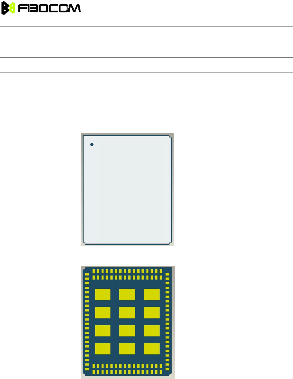
2.3 Pro
d
H330
H
Top Vi
e
Botto
m
Module Hard
w
• RoHS
• CE
• RRB
d
uct Ap
p
H
SPA+ Mod
u
e
w:
m
View:
w
are User M
a
p
earanc
e
u
le Appear
a
a
nual
e
a
nce is belo
w
w
。
Page 10 of 4
4
4
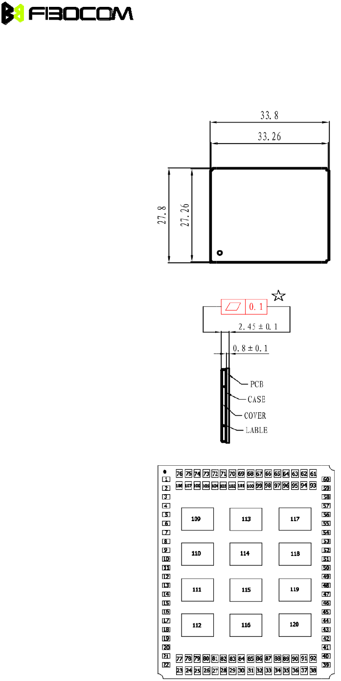
H330 HSPA+
3 Mec
h
3.1 Di
m
Module Hard
w
h
anical
m
ension
w
are User M
a
a
nual
Top View
Side View
Bottom Vie
w
w
Page 11 of 4
4
4
H330 HSPA+
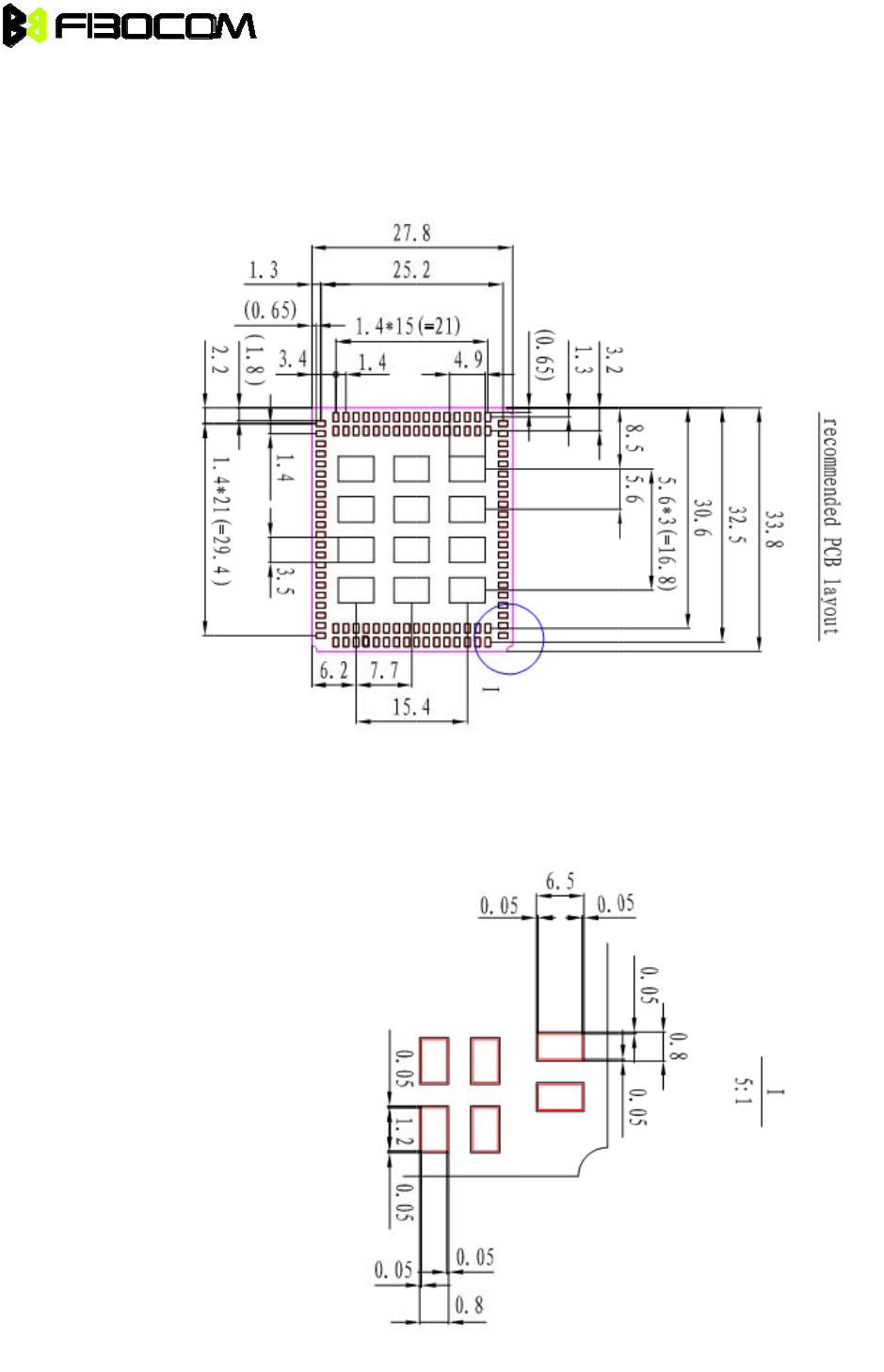
3.2 Re
c
Module Hard
w
c
ommen
d
w
are User M
a
d
PCB D
e
a
nual
e
sign
Page 12 of 4
4
4
H330 HSPA+
4 Har
d
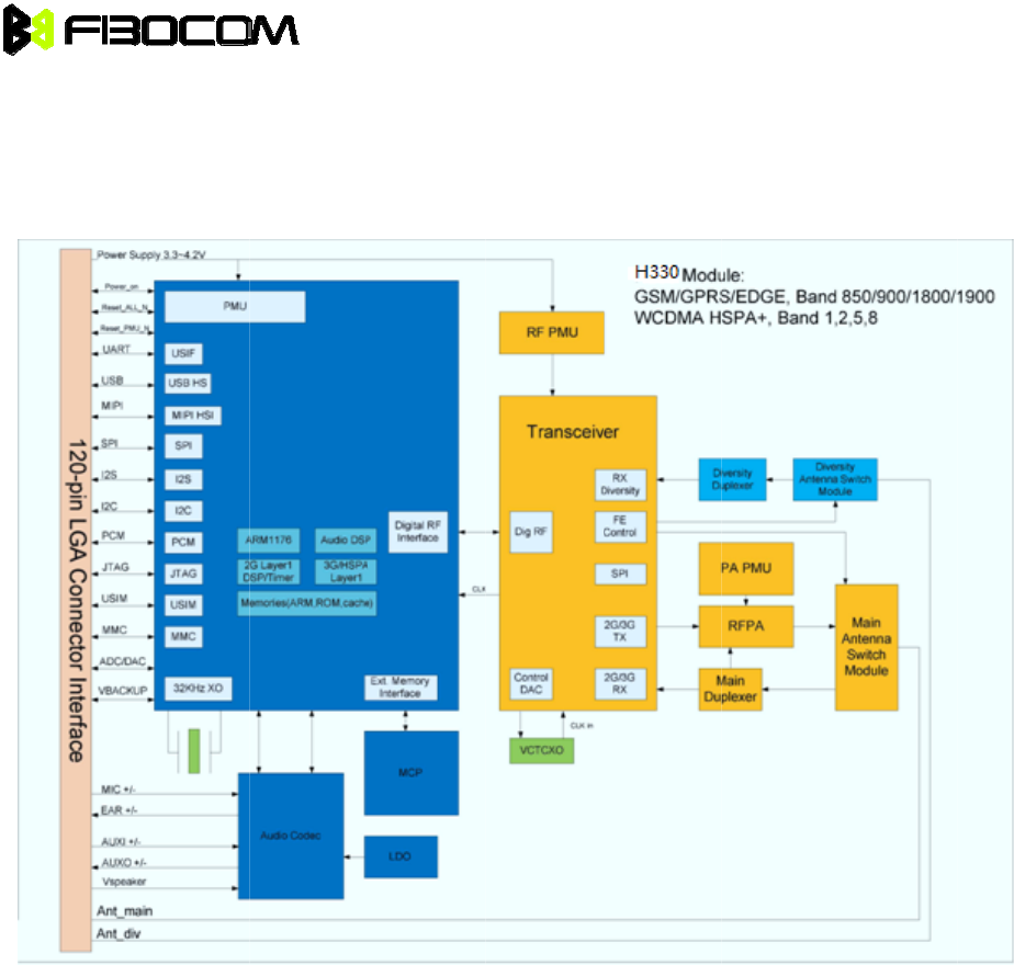
4.1 Blo
c
Module Hard
w
d
ware S
c
c
k Diagr
a
w
are User M
a
c
ope
a
m
a
nual
Page 13 of 4
4
4
H330 HSPA+
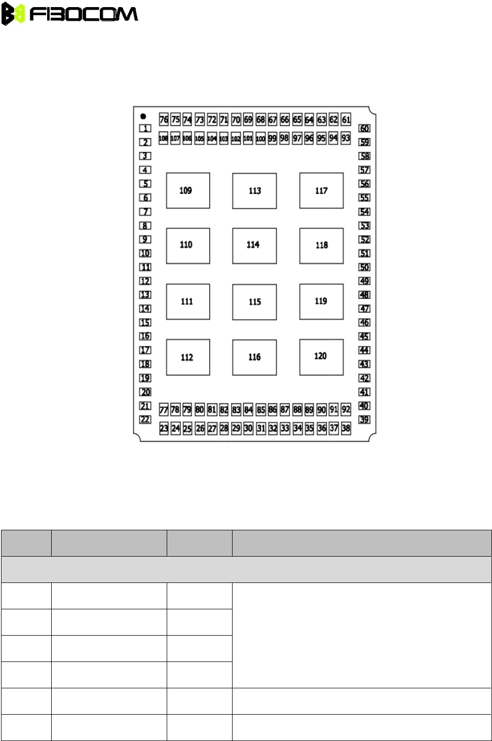
4.2 Pin
4.2.1 Pi
n
4.2.2 Pi
n
Notice: H3
3
H330 Pin d
e
Pin#
P
Power
59
V
60
V
61
V
62
V
64
V
1
V
Module Hard
w
Definiti
o
n
Map
n
Descript
i
3
0 logic ele
c
e
scription:
P
in Name
V
BAT
V
BAT
V
BAT
V
BAT
V
P
A
V
TRX
w
are User M
a
o
n
i
on
c
trical level i
s
a
nual
s
1.8V.
I/O
I
I
I
I
O
O
Descrip
t
Power s
u
Power s
u
Power s
u
t
ion
u
pply
u
pply indica
t
u
pply indica
t
t
or for RF P
A
t
or for RF tr
a
A
a
nsceive
r
Page 14 of 4
4
4

H330 HSPA+
46
V
47
V
On/off
48
P
49
P
Reset
77
R
USIM
4
U
5
U
6
U
7
U
8
U
High Spee
d
9
U
10
U
Audio
13
A
14
A
15
E
16
E
17
M
18
M
19
A
20
A
21
A
Module Hard
w
V
IO
V
RTC
P
OWER_O
F
P
OWER_O
N
R
ESET_AL
L
U
SIM_CD
U
SIM_VCC
U
SIM_RST
U
SIM_CLK
U
SIM_DAT
A
d
SIM
U
SIM_D+
U
SIM_D-
A
UXO+
A
UXO-
E
AR-
E
AR+
M
IC+
M
IC-
A
UXI-
A
UXI+
A
GND
w
are User M
a
F
F
N
L
_N
A
a
nual
O
I/O
I
I
I
I
O
O
O
I/O
O
O
O
O
I
I
I
I
GND
Digital p
o
Real tim
e
Off contr
o
On contr
o
External
USIM in
s
USIM p
o
USIM re
s
USIM cl
o
USIM d
a
High sp
e
High sp
e
Audio ch
Audio ch
Audio ch
Audio ch
Audio ch
Audio ch
Audio ch
Audio ch
Audio G
N
o
wer supply
e
clock pow
e
o
l signal
o
l signal
reset signal
s
ert detect, l
o
wer supply
s
et
o
ck
a
ta
e
ed SIM US
B
e
ed SIM US
B
annel2 out
p
annel2 out
p
annel1 out
p
annel1 out
p
annel1 inp
u
annel1 inp
u
annel2 inp
u
annel2 inp
u
N
D
1.8V.
er
,1.71V ~
ow activity
B
data line+
B
data line-
p
ut+
p
ut -
p
ut -
p
ut +
u
t +
u
t -
u
t -
u
t +。
1.89V
(No supp
o
(No suppo
r
Page 15 of 4
4
o
rt)
r
t)
4

H330 HSPA+
22
V
I2S
11 I
2
24 I
2
25 I
2
26 I
2
27 I
2
USB
31
U
32
U
33
U
34
V
92
U
I2C
28 I
2
29 I
2
UART1
35
U
36
U
37
U
38
U
39
U
40
U
41
U
42
U
UART2
Module Hard
w
V
SPK
2
S2_CLK1
2
S2_CLK0
2
S2_WA0
2
S2_TX
2
S2_RX
U
SB_DP
U
SB_DM
U
SB_ID
V
USB
U
SB_TEST
2
C_SDA
2
C_SCL
U
ART1_RI
U
ART1_DS
R
U
ART1_DT
R
U
ART1_DC
D
U
ART1_CT
S
U
ART1_RT
S
U
ART1_TX
D
U
ART1_RX
D
w
are User M
a
R
R
D
S
S
D
D
a
nual
I
O
O
O
O
I
I/O
I/O
—
I
—
I/O
O
O
I
O
O
I
O
O
I
Audio c
o
VBAT
I2S2 clo
c
I2S2 clo
c
I2S2 wo
r
I2S2 tra
n
I2S2 rec
e
USB dat
a
USB dat
a
USB ID l
USB po
w
USB TE
S
I2C data
I2C cloc
k
UART1
R
UART1
D
UART1
D
UART1
C
UART1
C
UART1
R
UART1
T
UART1
R
o
dec speak
e
c
k
c
k
r
d alignmen
t
n
smit line
e
ive line
a
line +
a
line -
ine
w
er supply
S
T line
line
k
line
R
ing indicat
o
D
TE Data S
e
D
CE Data T
e
C
arrier Dete
C
lear to sen
R
equest to
s
T
ransmitted
R
eceived D
a
e
r part powe
r
t
select
or
e
t ready
e
rminal rea
d
ct
d
s
end
Data
a
ta
r supply, co
n
d
y
Page 16 of 4
4
n
nect to
4

H330 HSPA+
45
U
44
U
ADC
50
A
51
A
EINT
56
W
57
E
USB HSIC
90
H
91
H
Antenna
67
A
71
A
Other
23
D
53
T
54
C
55
C
89
S
86
L
Not Conne
73
N
74
N
75
N
76
N
Module Hard
w
U
ART2_TX
D
U
ART2
_
RX
D
A
DC2
A
DC1
W
AKE_UP
E
INT2
H
SIC_USB
_
H
SIC_USB
_
A
NT_MAIN
A
NT_DIV
D
ACOUT
T
_OUT0
C
LKOUT0
C
LK32K
S
MI
L
PG
ct
N
C
N
C
N
C
N
C
w
are User M
a
D
D
_
DATA
_
STRB
a
nual
O
I
I
I
I
I
I
O
UART2
T
UART2
R
Analog
d
Analog
d
Wake u
p
External
HSIC U
S
HSIC U
S
Main ant
Diversity
No Sup
p
No supp
o
No supp
o
No supp
o
Sleep M
o
Module
w
T
ransmitted
R
eceived D
a
d
igital conve
d
igital conve
p
signal, low
interrupt, lo
w
S
B data sig
n
S
B pulse sig
enna port,
5
antenna p
o
p
ort
o
rt
o
rt
o
rt
o
de Indicat
o
w
ord mode i
Data
a
ta
r
ter 2(No
s
r
ter 1(No
s
activit
y
.
w
activit
y
.
n
al(No sup
p
nal(No su
p
5
0ohm imp
e
o
rt, 50ohm i
m
or
ndicato
r
s
upport)
s
upport)
p
ort)
p
port)
e
dance
m
pedance
Page 17 of 4
4
4

H330 HSPA+
105
N
106
N
107
N
108
N
78
N
79
N
80
N
81
N
82
N
83
N
84
N
85
N
87
N
88
N
94
N
95
N
96
N
101
N
GND
2
G
12
G
21
G
30
G
43
G
58
G
63
G
Module Hard
w
N
C
N
C
N
C
N
C
N
C
N
C
N
C
N
C
N
C
N
C
N
C
N
C
N
C
N
C
N
C
N
C
N
C
N
C
G
ND
G
ND
G
ND
G
ND
G
ND
G
ND
G
ND
w
are User M
a
a
nual
Page 18 of 4
4
4

H330 HSPA+
65
G
66
G
68
G
69
G
70
G
72
G
93
G
97
G
98
G
99
G
100
G
102
G
103
G
104
G
109
G
110
G
111
G
112
G
113
G
114
G
115
G
116
G
117
G
118
G
119
G
120
G
Module Hard
w
G
ND
G
ND
G
ND
G
ND
G
ND
G
ND
G
ND
G
ND
G
ND
G
ND
G
ND
G
ND
G
ND
G
ND
G
ND
G
ND
G
ND
G
ND
G
ND
G
ND
G
ND
G
ND
G
ND
G
ND
G
ND
G
ND
w
are User M
a
a
nual
Page 19 of 4
4
4

H330 HSPA+
5 Har
d
5.1 Po
w
5.1.1
V
B
A
The H330
p
must be ab
l
2.0A.
It is require
m
Parame
t
VBAT
Special car
e
source indi
r
amplifier (P
A
transients,
w
The burst-
m
from the po
w
transmissio
drop. If the
v
performanc
It is recom
m
H330 interf
a
In any case
burst. Drop
p
an automat
i
To minimiz
e
guidelines:
Use a
1
locate
d
Use lo
w
Use ca
Filter t
h
Module Hard
w
d
ware In
w
er Inter
f
A
T
p
ower suppl
y
l
e to sustai
n
m
ent below
:
t
e
r
M
3
e
must be t
a
r
ectly suppli
e
A
). Therefo
r
w
ill directly
a
m
ode operat
w
er supply,
n bursts co
n
v
oltage dro
p
e.
m
ended that
a
ce connec
t
, the H330
s
p
ing below t
i
c power-off
e
the losses
1
000 uF, or
g
d
as near to
w
impedanc
e
bling and r
o
h
e H330 su
p
w
are User M
a
terface
f
ace
y
must be a
n
the voltag
e
:
M
in.
3
.6
a
ken when
d
e
s all the di
g
r
e, any degr
a
ffect the H
3
ion of the G
which caus
e
n
sume the
m
p
s are not
m
the voltage
t
or.
s
upply input
he minimu
m
.
and transie
g
reater, low
the H330 in
e
power so
u
o
uting as sh
o
p
ply lines u
s
a
nual
single exte
r
e
level durin
g
Re
c
3.8
d
esigning th
e
g
ital and an
a
adation in t
h
3
30 perform
SM transmi
s
e
s tempora
r
m
ost instant
a
m
inimized, t
h
drops duri
n
must not d
r
m
operating l
nts on the
p
ESR capa
c
terface con
n
u
rce, cablin
g
o
rt as possi
b
s
ing filtering
r
nal DC volt
a
g
a GSM tr
a
c
ommend
e
power su
p
a
log interfa
c
h
e power su
ance.
s
sion and r
e
r
y voltage d
r
a
neous cur
r
h
e frequent
v
n
g a transmi
t
r
op below t
h
evel may r
e
p
ower suppl
y
c
itor on the
H
n
ector as p
o
g
and board
b
le.
capacitors,
a
ge source
a
nsmit burst
Max.
4.2
p
ply of the
H
c
es, but als
o
pply perfor
m
e
ception dr
a
r
ops of the
p
r
ent, and th
e
v
oltage
f
luc
t
t
burst will n
h
e minimum
e
sult in a lo
w
y
lines, it is
r
H
330 suppl
y
o
ssible.
routing.
as describe
of 3.6V to 4
current ser
g
H
330. The si
o
directly su
p
m
ance, due
a
ws instanta
p
ower suppl
e
refore caus
t
uations ma
y
ot exceed
3
operating l
e
w
voltage de
t
r
ecommend
y
inputs. Th
e
d in the tab
l
.2V. The po
w
g
e, which m
Unit
V
ngle extern
a
p
plies the
R
to losses, n
neous curr
e
y level. The
e the large
s
y
degrade t
h
3
00mV, mea
s
e
vel during
a
t
ection, whi
c
ed to follow
e
capacitor
s
l
e.
Page 20 of 4
4
w
er supply
ay reach
a
l DC powe
r
R
F power
oises or
e
nt surges
s
t voltage
h
e H330
s
ured on th
e
a
transmit
c
h will initiat
e
these
s
hould be
4
r
e
e

H330 HSPA+
Recom
Capacit
o
1000uF
10nF, 1
0
8.2pF, 1
33pF, 3
9
5.1.2 Po
w
Parame
t
I off
I idle
I sleep
IGSM-RMS
Module Hard
w
mended
or
0
0nF
0pF
9
pF
w
er Cons
u
t
e
r
De
s
RT
C
Idl
e
Lo
w
mo
GS
1
T
1
R
w
are User M
a
Usage
GSM Tr
a
s
Digital s
w
1800/19
0
b
850/900 M
u
mption
s
cription
C
mode
e
mode
w
power
de
M voice -
T
X slot
R
x slot
a
nual
a
nsmit curre
s
erge
w
itching noi
s
0
0 MHz GS
M
b
ands
Hz GSM ba
Conditi
o
DRX
DRX
DRX
GSM85
0
EGSM9
0
DCS18
0
Des
c
nt Mini
m
burs
t
s
e Filte
r
sour
c
M
Filte
r
nds Filte
r
o
n
0
PCL
0
0 PCL
0
0 PCL
c
ription
m
izes pow
e
t
s. Use max
r
s digital lo
g
c
es.
r
s transmis
s
r
s transmis
s
T
5
2
2
2
5
2
9
2
5
2
10
7
15
4
19
4
5
2
10
7
15
4
19
4
0
5
6
10
4
e
r supply lo
s
imum possi
g
ic noises f
r
s
ion EMI.
s
ion EMI.
T
ypical
5
3uA
2
0.4
2
.0
2
.0
2
.0
2
22.8
7
7.8
4
8.9
4
4.9
2
29.8
7
8.3
4
5.3
4
4.3
152.0
6
8.0
4
7.1
s
ses during
ble value.
r
om clocks
Unit
uA
mA
mA
mA
Page 21 of 4
4
transmit
and data
4

H330 HSPA+
IGPRS-RM
S
IEGPRS-R
M
Module Hard
w
S
G
P
-
4
T
1
R
M
S
EG
12
4
T
1
R
w
are User M
a
P
RS Class 1
2
T
X slot
R
x slot
PRS Class
-
T
X slot
R
x slot
a
nual
PCS19
0
2
GSM85
0
EGSM9
0
DCS18
0
PCS19
0
GSM85
0
EGSM9
0
0
0 PCL
0
PCL
0
0 PCL
0
0 PCL
0
0 PCL
0
PCL
0
0 PCL
15
4
0
5
6
10
4
15
4
5
5
10
2
15
19
9
5
5
10
2
15
19
9
0
3
5
10
9
15
8
0
3
5
10
15
9
8
4
14
19
9
8
5
14
4
5.0
150.9
6
8.6
4
7.1
4
4.6
5
65.1
2
13.6
105.4
9
1.3
5
83.4
2
17.7
105.5
9
11.0
3
53.5
167.6
9
5.3
8
6.3
3
73.7
174.4
100.4
9
1.6
4
88.7
142.4
9
0.9
5
04.7
146.9
mA
mA
Page 22 of 4
4
4

H330 HSPA+
IGSM-MAX
IWCDMA-R
M
Module Hard
w
Pe
a
Du
r
M
S W
C
w
are User M
a
a
k current
r
ing TX slot
C
DMA
a
nual
DCS18
0
PCS19
0
GSM85
0
EGSM9
0
DCS18
0
PCS19
0
Band5 (
8
0
0 PCL
0
0 PCL
0
PCL
0
0 PCL
0
0 PCL
0
0 PCL
8
50)
19
9
2
4
9
15
9
2
4
9
15
9
5
10
3
15
19
9
5
10
3
15
9
19
9
0
9
5
2
10
15
9
0
9
5
2
10
15
9
24dBm
4
0dBm
-24dBm
9
1.2
4
98.4
104.6
9
1.0
4
96.9
113.1
9
8.4
1556.4
3
50.2
120.5
9
1.3
1595.4
3
58.8
9
0.9
9
7.9
9
52.9
2
70.6
115.1
9
2.4
9
57.2
2
78.1
110.6
9
2.4
4
55.7
142.0
135.4
mA
mA
Page 23 of 4
4
4
H330 HSPA+
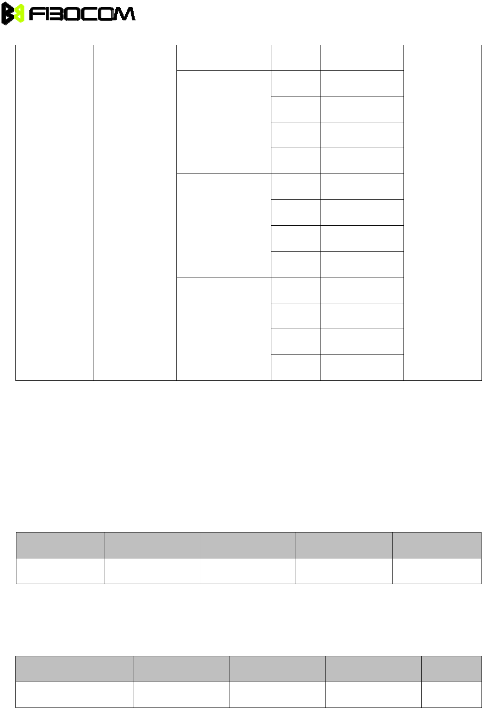
5.1.3
V
I
O
The H330 i
n
the custom
e
It is for mo
d
digital sign
a
Parame
t
VIO @
w
5.1.4
V
R
T
VRTC is a
p
Parame
t
VRTC
O
Module Hard
w
O
n
corporates
e
r applicati
o
d
ule to pow
e
a
l.
t
e
r
M
w
orking
1
T
C
p
owe
r
suppl
t
e
r
O
utput Volta
g
w
are User M
a
a regulate
d
o
n. It can be
e
r supply di
g
M
in.
1
.773
y for modul
e
Min.
g
e 1.71
a
nual
Band2 (
1
Band1 (
2
Band8 (
9
d
voltage ou
t
used as a i
n
g
ital signal i
n
Ty
p
1.8
e
RTC circu
1
900)
2
100)
9
00)
t
put VIO. T
h
n
dicator.
n
ternal H33
0
p
ical
it and can b
Typical
1.8
-50dBm
24dBm
5
0dBm
-24dBm
-50dBm
24dBm
5
0dBm
-24dBm
-50dBm
24dBm
4
0dBm
-24dBm
-50dBm
h
e regulator
0
, so it can
b
Max.
1.82
7
e connect t
o
133.7
5
12.5
146.3
137.2
135.6
5
64.2
117.1
105.4
103.4
4
31.9
142.3
135.8
134.1
provides a
1
b
e used as
a
7
o
external
R
Max.
1.89
1
.8V output
a
reference
Unit
V
R
TC battery.
U
V
Page 24 of 4
4
for use by
level for
U
nit
V
4
H330 HSPA+
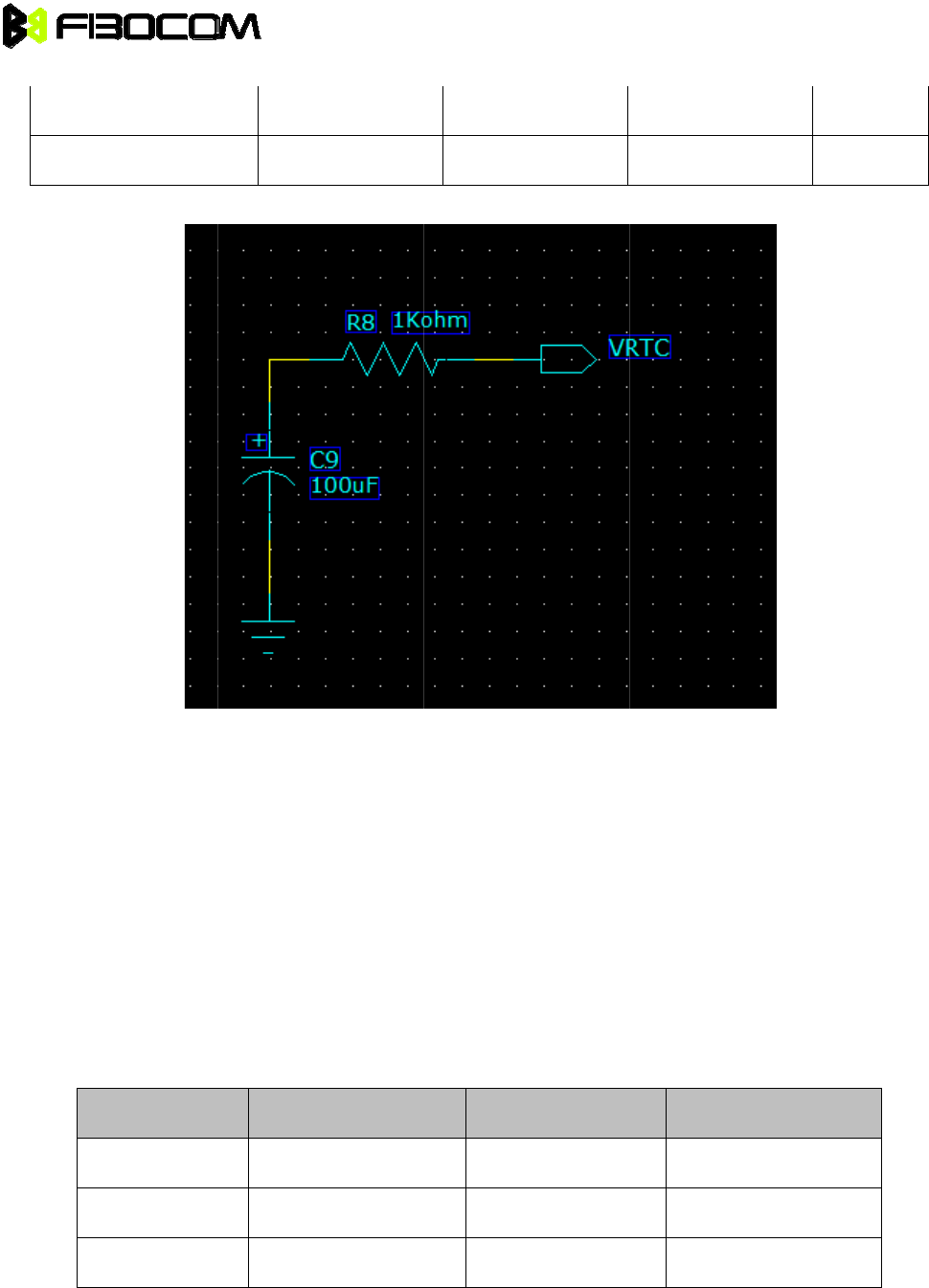
VRTC I
n
(RTC is
w
VRTC I
n
(RTC is
w
VRTC refer
e
Notes:
R8 is limite
d
VRTC cons
C9 can det
e
5.2 On/
O
5.2.1 Pi
n
H330 has 3
Pin definiti
o
Pi
n
48
49
77
Module Hard
w
n
put Voltag
e
w
orking)
n
put Curren
t
w
orking)
e
nce desig
n
d
resistor.
umption cu
r
e
rmine the r
e
O
ff/Res
e
n
Descript
i
control sig
n
o
n is below:
n
#
w
are User M
a
e
0.5
t
n
is below:
r
rent is less
e
served tim
e
t
i
on
n
als to on,
o
Pin Na
POWE
POWE
RESE
T
a
nual
than 2uA.
e.
o
ff ,reset mo
d
me
R_OFF
R_ON
T
_ALL_N
1.8
d
ule.
Elect
r
CMO
S
CMO
S
CMO
S
r
ical Level
S
1.8V
S
1.8V
S
1.8V
1.89
1.5
Descr
Off co
n
On co
n
Exter
n
V
u
A
iption
n
trol signal
n
trol signal
n
al reset sig
n
Page 25 of 4
4
V
A
n
al
4
H330 HSPA+
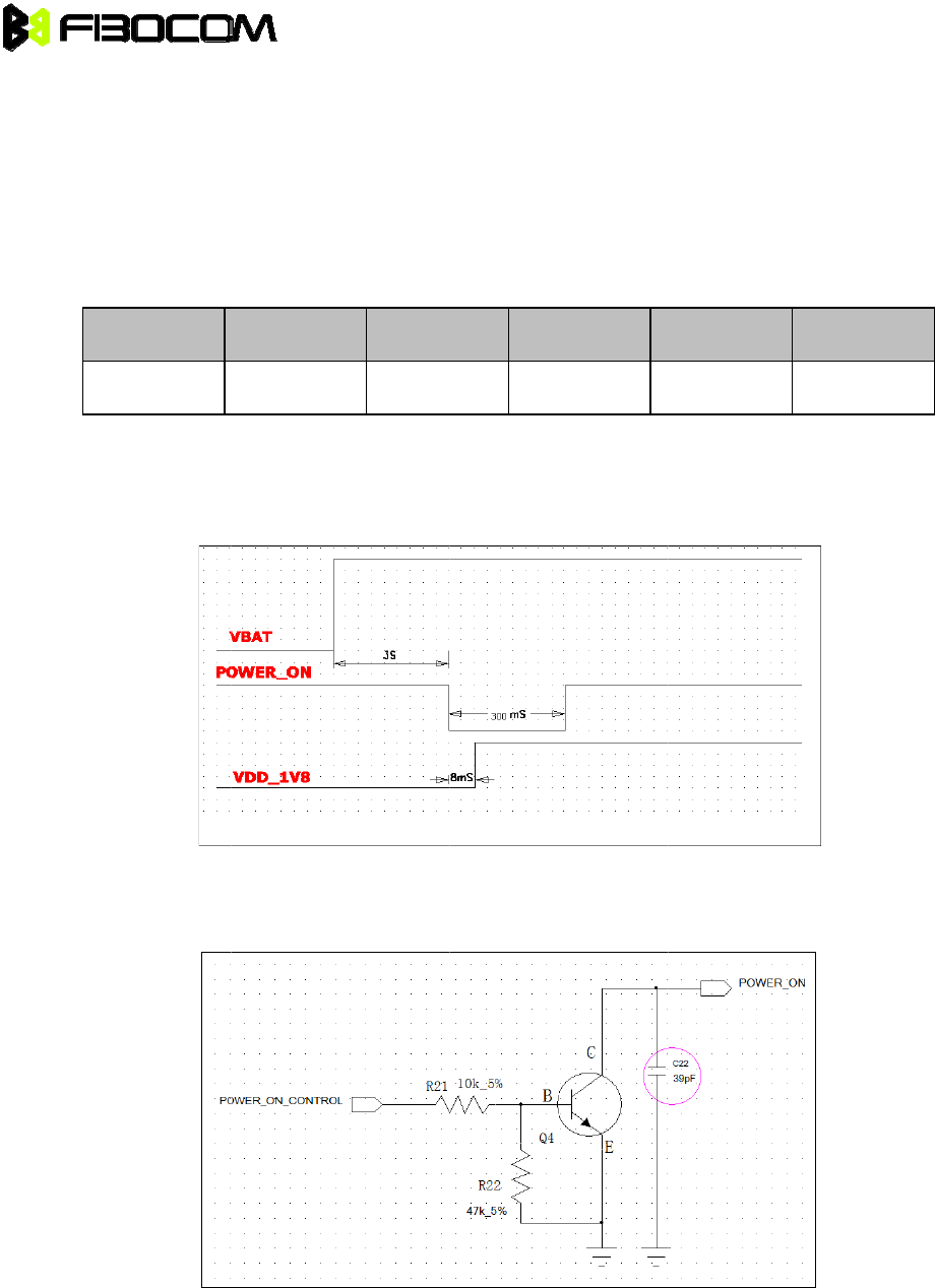
5.2.2 Po
w
When the
H
H330 will p
o
low for a mi
Pa
r
Pu
l
Control timi
Recomman
5.2.3 Po
w
When
s
Module Hard
w
w
er on
H
330 is pow
e
o
wer on ag
a
nimum of 1
0
r
amete
r
l
se width
ng is below
:
d Design:
w
er of
f
s
et POWE
R
w
are User M
a
e
red off, th
e
a
in when th
e
0
0 millisec
o
Condition
:
R_
OFF to lo
w
a
nual
e
PMU oper
a
e
POWER_
O
o
nds will tu
r
Min.
100
w
level, H33
a
tes at low
p
O
N signal is
r
n H330 on
Typ
i
300
0 will be po
w
p
ower mode
falling edg
e
i
cal
M
w
er down.
, with only t
h
e
. Asserting
M
ax
h
e RTC tim
e
the POWE
R
Unit
ms
Page 26 of 4
4
e
r active.
R
_ON signa
4
l
H330 HSPA+
Pa
r
Pu
l
Control timi
Recomman
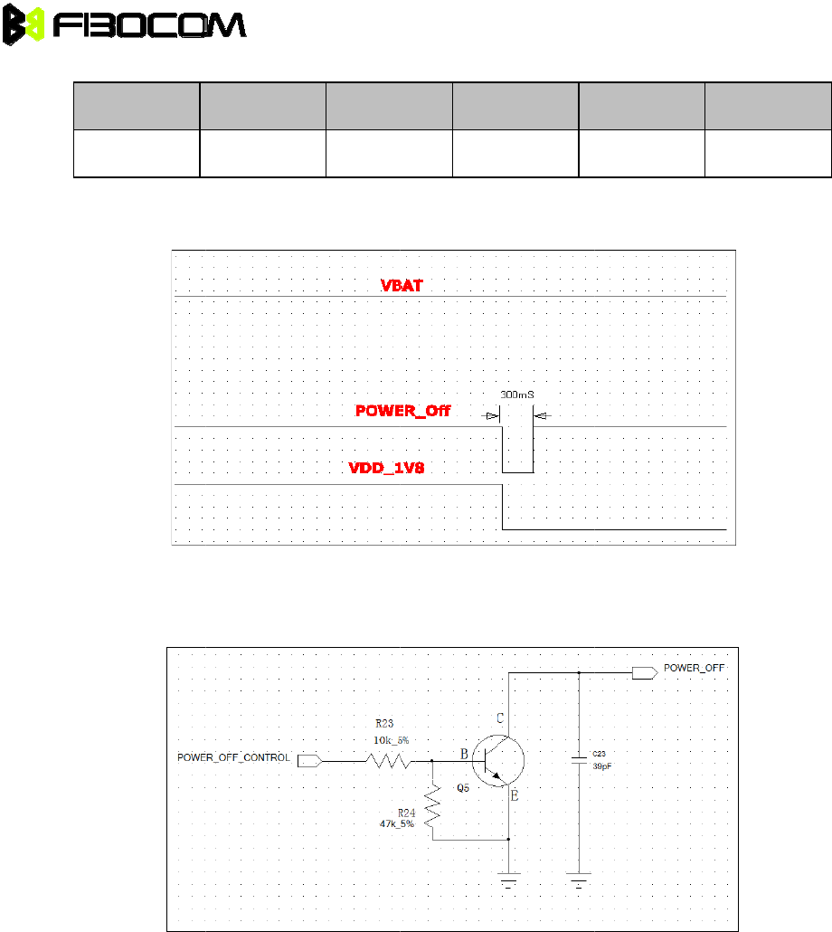
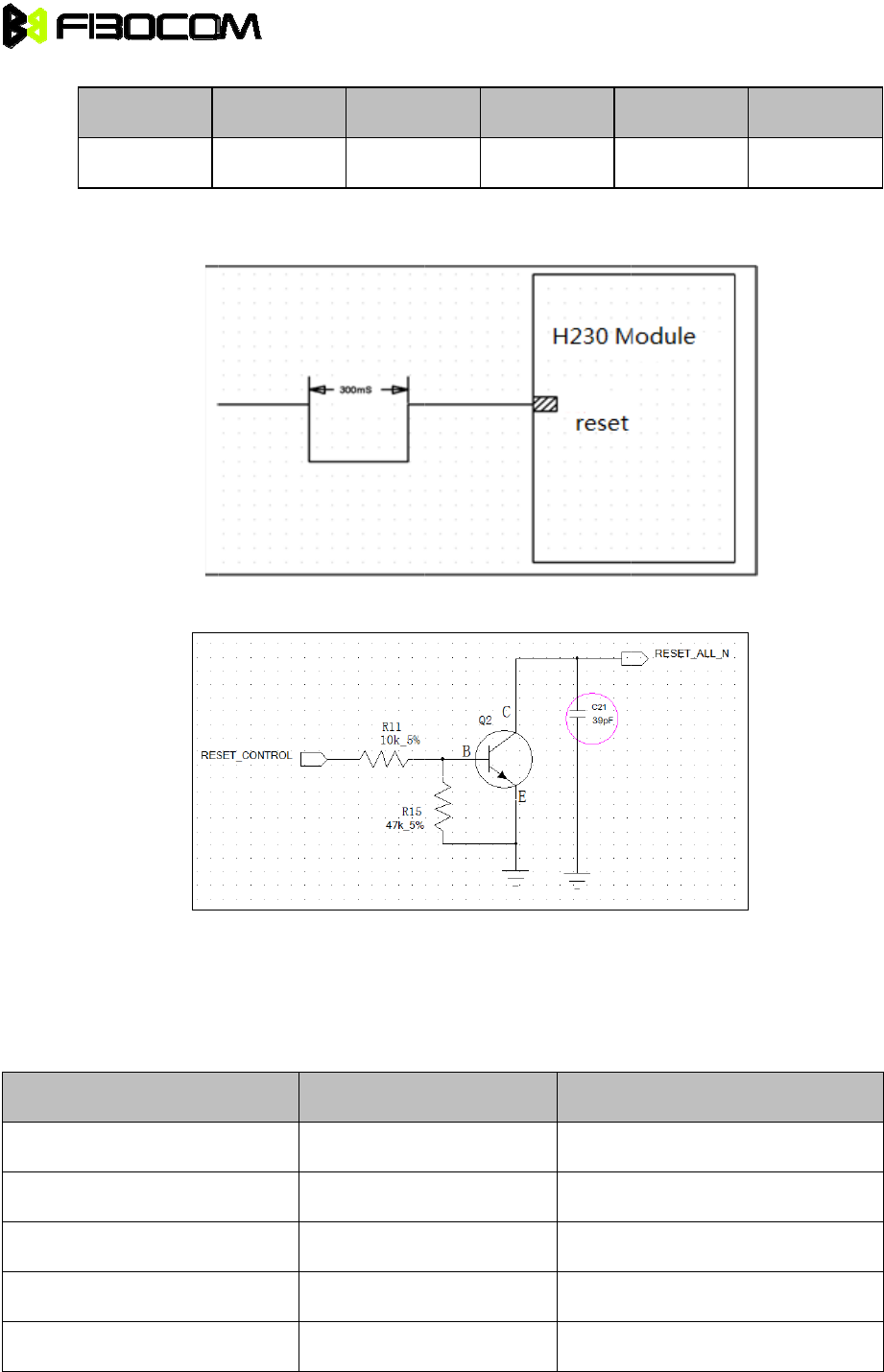
5.2.4 Re
s
The RESE
T
H330 is res
Important:
The reset s
i
It’s recomm
Module Hard
w
r
amete
r
l
se width
ng is below
:
d Design:
s
et
T
_N input si
g
et without t
h
i
gnal is ver
y
ended that
w
are User M
a
Condition
:
g
nal would
b
h
e work net
y
important f
o
it should co
n
a
nual
Min.
100
b
e reset the
logging out.
o
r the syste
n
nect he 33
/
Typ
i
300
H330 imm
e
m. When d
e
/
39pF capa
c
i
cal
M
3
e
diately. Wh
e
e
sign it nee
d
c
ito
r
to GN
D
M
ax
3
000
e
n the RES
d
be protect
e
D
on extern
a
Unit
ms
ET_N sign
a
e
d totally.
a
l circuit.
Page 27 of 4
4
a
l is low, the
4
H330 HSPA+
Pa
r
Pu
l
Control timi
Recomman
5.3 Indi
5.3.1 Pi
n
Pin#
86
89
56
1
64
Module Hard
w
r
amete
r
l
se width
ng is below
:
d Design:
cator Si
g
n
Descript
i
w
are User M
a
Condition
:
g
nal
i
on
P
L
S
W
V
V
a
nual
Min.
100
P
in Name
PG
MI
W
AKE_UP
V
TRX
V
P
A
Typ
i
300
i
cal
M
3
Descri
p
Work
m
Sleep
M
Wake
u
Power
s
transc
e
Power
s
M
ax
3
000
p
tion
m
ode indicat
o
M
ode Indica
u
p module
s
upply indi
c
e
ive
r
s
upply indi
c
Unit
ms
or
to
r
c
ator for
c
ator for RF
Page 28 of 4
4
P
A
4

H330 HSPA+
5.3.2 Ind
5.3.2.1 L
P
LPG worki
n
State
• NO SIM c
a
• SIM Error
• Registerin
g
• Register n
(always)
• IDLE mod
e
• Calling
• Data com
m
• Calling Sl
e
Notice:Hi
g
5.3.2.2 S
M
Module
Mode
Sleep Mod
e
Other Mod
e
5.3.2.3 W
A
Module
Mode
Sleep
Idle/Call
Module Hard
w
icator De
s
P
G
n
g state des
c
a
rd
g
network
etwork failu
r
e
m
unicating
e
ep
g
h level is 1
.
M
I
SMI
W
e
2.5S
H
e
Low
A
KE_UP
WAK
E
Low
High
Low
High
w
are User M
a
s
cription
c
ription is b
e
W
r
e
6
0
7
5
L
o
7
5
H
.
8V.
W
orking mo
d
H
igh; 100ms
E
_UP
a
nual
e
low:
W
ork mode
0
0ms High,
5
ms High,
3
o
w
5
ms High,
7
H
igh
d
e
Low
Worki
n
Wake
u
Keep
S
Keep
m
Modul
e
600ms Lo
w
3
S Low
7
5ms Low
n
g Descrip
t
u
p the mod
u
S
leep mode
m
ode, no af
f
e
cannot set
w
t
ion
u
le, from Sl
e
f
ect
to Sleep m
o
e
ep to Idle
o
de
Page 29 of 4
4
4
H330 HSPA+
5.3.2.4 O
t
Pin Name
VTRX
VPA
Notice:
5.4 US
B
5.4.1 US
Pin#
31
32
33
34
92
H330 can s
When H33
0
1
p
2
p
2
p
2
p
5.4.2 US
Reference
D
Module Hard
w
t
he
r
Electr
i
1.8V
0-4.3V
They are i
n
B
Interfa
c
B Pin De
s
Pin N
a
USB_
D
USB_
D
USB_
I
VUSB
USB_
T
upport USB
0
connect to
p
ort is for 3
G
p
orts are fo
r
p
orts are fo
r
p
orts are re
s
B Design
D
esign:
w
are User M
a
i
cal Level
n
dicator sig
n
c
e
s
cription
a
me
D
P
D
M
I
D
T
EST
2.0. It is ne
e
PC by US
B
G
Modem to
r
AT Comm
a
r
trace.
s
erved.
a
nual
Descri
RF Tra
It work
s
0.65
V
it is 0
V
n
al, it canno
t
I/O
I/O
I/O
—
I
—
e
d to install
B
, PC will g
e
do data op
e
a
nd.
ption
nsceiver P
M
s
in Tx mod
e
V
, when the
m
V
t
be used fo
Des
c
USB
USB
USB
USB
USB
USB driver.
e
t 7 port blo
w
e
ration
M
U work ind
e
, when the
m
ax. power
r other, it c
a
c
ription
signal +
signal -
ID signal
power sup
p
TEST sign
a
w
:
icato
r
low power
i
it is about 4
.
a
n be set N
C
p
ly
a
l
i
t is about
.3V, other
m
C
.
Page 30 of 4
4
m
ode
4
H330 HSPA+
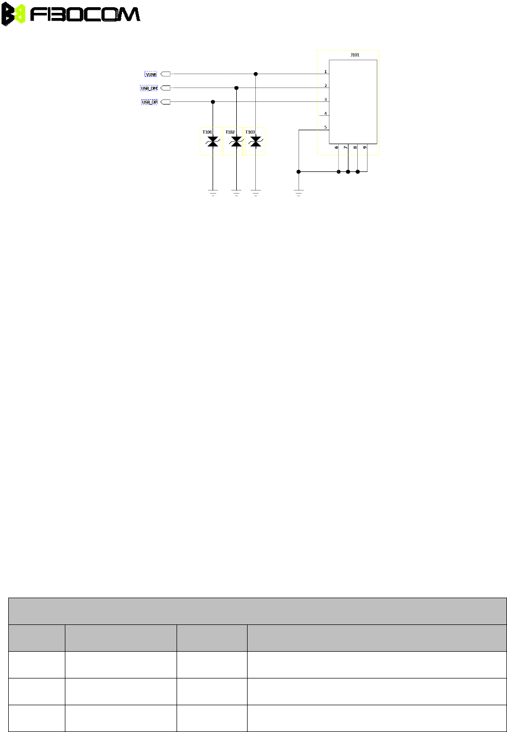
T101 and T
VUSB is U
S
Notice:
VUSB sho
u
USB_DP a
n
T
h
pr
o
It i
s
po
Y
o
D
u
In
t
5.5 UA
R
5.5.1 UA
H330 sup
p
8 l
2 l
UART1
UART1
Pin#
35
36
37
Module Hard
w
102 should
S
B power s
u
u
ld be conn
e
n
d USB_D
M
h
e layout de
s
o
tocol, with
d
s
recomme
n
ints on the
A
o
u don’ t ne
e
u
e to the us
e
t
erface of v
e
R
T
RT Interf
a
p
ort 2 UAR
T
ines UART
1
ines UART
2
and UART
Pin Nam
e
UART1_
R
UART1_
D
UART1_
D
w
are User M
a
be low cap
a
u
pply, it is 2.
e
ct to a level
M
are high s
p
s
ign of this
c
d
ifferential l
n
ded that s
e
A
P for debu
g
e
d to conne
c
e
d enclosur
e
e
rsion 2.0 o
r
a
ce
T
, one is 8 li
n
1
support fl
o
2
only supp
o
2 defined b
e
e
R
I
D
SR
D
TR
a
nual
a
cito
r
TVS, i
5V ~ 5.25V.
(2.5V ~ 5.
2
p
eed lines, i
t
c
ircuit on th
e
ining and i
m
e
t USB_DP
a
g
.
c
t the USB_
V
e
material, t
h
r
higher. Th
e
n
es ; the ot
h
o
w control, c
o
rt AT
e
low:
I/O
O
I
O
t is below 1
2
5V) or US
B
t
is 480 Mb
p
e
AP board
s
m
pedance c
o
a
nd USB_D
V
BUS whe
n
h
e mobile p
e
connectio
n
h
er is 2 line
s
an be used
Desc
r
UART
UART
UART
pF.
B
cannot be
r
p
s, It is PC
B
s
hould com
p
o
ntrol to 90
o
M pins as t
e
n
the functio
n
h
one shall
o
n
to so calle
d
s
。
to downloa
d
iption
1 Ring indi
c
1 DTE Data
1 DCE Dat
a
r
ecognized.
B
Layout req
p
ly with the
o
hm.
e
st points a
n
n
of USB is
o
nly be con
n
d
power US
B
d
or AT com
c
ato
r
Set ready
a
Terminal r
e
uirement b
e
USB 2.0 hi
g
n
d then pla
c
not used.
n
ected to a
U
B
is prohibi
t
munication.
e
ady
Page 31 of 4
4
e
low:
g
h speed
c
e these tes
t
U
SB
ed.
4
t
H330 HSPA+
38
39
40
41
42
UART2
Pin#
44
45
5.5.2 UA
H330(DC
E
Appl
i
RXD
TXD
RTS
CTS
DSR
DTR
RI
DCD
H330(DC
E
Appl
i
RXD
TXD
Module Hard
w
UART1_
D
UART1_
C
UART1_
R
UART1_
T
UART1_
R
Pin Nam
e
UART2_
R
UART2_
T
RT Desig
n
E
)UART1
c
i
cation MC
U
E
)UART2
c
i
cation MC
U
w
are User M
a
D
CD
C
TS
R
TS
T
XD
R
XD
e
R
XD
T
XD
n
c
onnect to
P
U
(DTE)
c
onnect to
P
U
(DTE)
a
nual
O
I
O
O
I
I/O
I
O
P
C(DTE)
,
Signal di
r
P
C(DTE)
,
Signal di
r
UART
UART
UART
UART
UART
Desc
r
UART
2
UART
2
,
the signal
d
r
ection
,
the signal
d
r
ection
1 Carrier D
e
1 Clear to s
e
1 Request t
o
1 Transmitt
e
1 Received
iption
2
Transmitt
e
2
Received
d
irection is
b
H3
3
UA
UA
UA
UA
UA
UA
UA
UA
d
irection is
b
H3
3
UA
UA
e
tect
e
nd
o
send
e
d Data
Data
e
d Data
Data
b
elow:
3
0 Module
(
RT1_TXD
RT1_RXD
RT1_CTS
RT1_RTS
RT1
_
DTR
RT1
_
DSR
RT1_RI
RT1_DCD
b
elow:
3
0 Module
(
RT2_TXD
RT2_RXD
(
DCE)
(
DCE)
Page 32 of 4
4
4
H330 HSPA+
Notice:
H330 UAR
T
If DTE is n
o
When use i
t
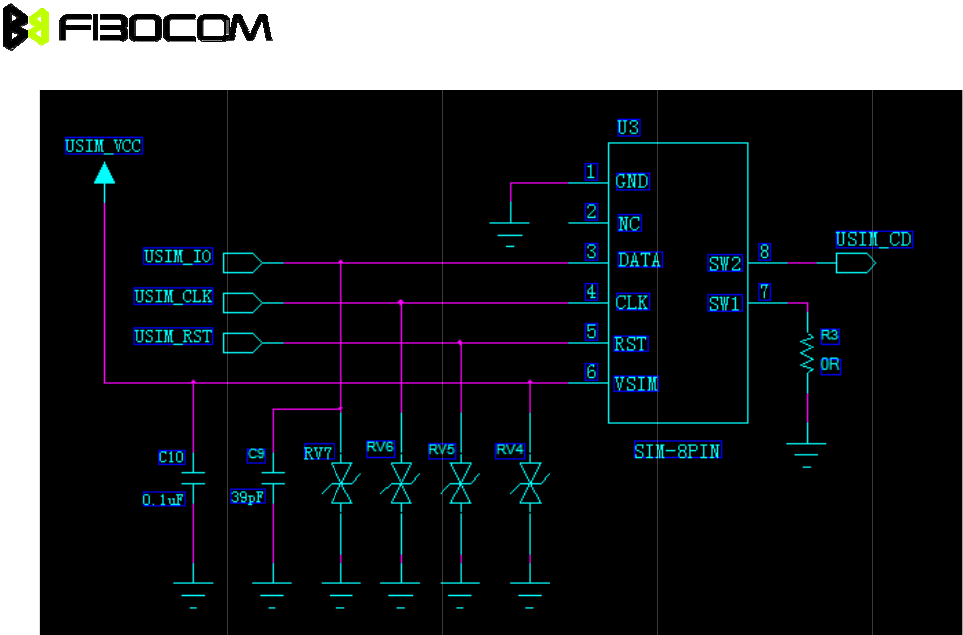
5.6 USI
M
H330
s
5.6.1 US
I
P
5
6
7
8
1
4
5.6.2 US
I
Reference
d
Module Hard
w
T
high level
i
o
t suitable,
n
t
, need car
e
M
s
upport USI
M
I
M Interfa
c
P
in#
5
6
7
8
2
4
I
M Desig
n
d
esign:
w
are User M
a
i
s 1.8V.
n
eed add el
e
e
about the
s
M
,now don’
c
e
Pin Nam
USIM_V
C
USIM_R
S
USIM_C
L
USIM
_
I
O
GND
USIM_C
D
n
a
nual
e
ctrical level
s
ignal direct
i
t support hi
g
e I/
O
C
C O
S
T O
L
K O
O
I/
O
G
D
I
translation
.
i
on.
g
h speed SI
O
O
ND
.
M.
Descri
p
USIM p
o
USIM R
e
USIM cl
o
USIM d
a
USIM g
r
USIM in
s
p
tion
o
wer supply
e
set signal
o
ck signal
a
ta signal
r
ound
s
ert detect
s
output
s
ignal
Page 33 of 4
4
4
H330 HSPA+
Notice:
5.6.3 US
I
The SIM in
t
card. There
meets the r
e
T
h
so
T
h
co
To
re
c
su
T
h
el
e
(T
D
Module Hard
w
USIM_IO
USIM_C
D
I
M Desig
n
t
erface and
s
are several
e
quired sta
n
h
e SIM shou
urces, such
h
e SIM inter
f
nnector an
d
avoid cros
s
c
ommende
d
rrounding g
r
h
e SIM card
e
ments (ze
n
D
K). We al
s
w
are User M
a
is pulled u
p
D
can suppo
n
Notice
s
ignals desi
design gui
d
n
da
r
ds and
r
ld be locate
as the RF
a
f
ace signals
d
the SIM tr
a
s
talk betwe
e
d
to rout the
m
r
ound plan
e
signals sho
n
er diodes,
e
s
o recomme
n
a
nual
p
internal H
3
rt SIM hot
p
gn is extre
m
d
elines that
m
r
egulations.
d, and its si
g
a
ntenna an
d
length sho
u
a
y. This is to
e
n the SIM
c
m
separatel
y
e
.
uld be prot
e
e
tc.). The re
c
n
ded the E
S
3
30.
p
lug, low is
a
m
ely import
a
m
ust be foll
o
g
nals shoul
d
d
digital swit
c
u
ld not exce
meet with
E
c
lock and d
a
y
on the ap
p
e
cted from
E
c
ommende
d
S
D compon
e
a
ctive and S
a
nt for prop
e
o
wed to ac
h
d
be routed,
c
hing signa
l
ed 100 mm
E
MC regula
t
ta signals (
S
p
lication bo
a
E
SD using v
e
d
part no of
E
e
nt should l
a
IM card is i
n
e
r operation
h
ieve a robu
s
away from
l
s.
between th
e
t
ions and i
m
S
IM_CLK a
n
a
rd, and pre
f
e
ry low cap
a
E
SD is AV
R
a
yout with
S
n
serted。
of H330 an
d
s
t and stabl
e
any possibl
e
H330 inte
r
m
prove sign
a
n
d SIM_DA
T
f
erably isol
a
a
citance pr
o
R
-M1005C0
8
S
IM hold clo
s
Page 34 of 4
4
d
the SIM
e
design th
a
e EMI
r
face
a
l integrity.
T
A), it is
a
ted by a
o
tective
8
0MTAAB
s
ely.
4
a
t

H330 HSPA+
5.6.4 US
I
H330 supp
o
5.6.4.1 H
a
When SIM
i
In referenc
e
When no S
I
5.6.4.2 S
o
When set
AT
detected wi
t
SIM_CD=L
o
SIM_CD=H
Important:
disabled co
5.7 An
a
5.7.1 Pi
n
The H330
a
interface's
o
fully control
commands
Pin#
13
14
15
16
17
18
19
20
Module Hard
w
I
M Hot Pl
u
o
rt SIM hot
p
a
rdware De
i
s removed,
e
design US
I
M card, S
W
o
ftware De
s
AT
+MSMPD
=
t
h SIM_CD
o
w level, SI
M
igh or NC,
S
The defa
u
rrespondin
g
a
log Aud
n
Descript
i
a
udio interfa
c
o
perating m
o
led by the h
set.
Pin Na
m
AUXO+
AUXO-
EAR-
EAR+
MIC+
MIC-
AUXI-
AUXI+
w
are User M
a
u
g
p
lug.
sign
USIM_CD i
IM_CD con
n
W
2 is high; I
n
s
ign
=
1, the SIM
pin.
M
card is o
n
S
IM card is
o
u
lt value of
M
g
ly.
io
i
on
c
e supports
o
des, activ
e
ost applicat
m
e
a
nual
s high; inse
n
ect U3 Pin
8
n
sert SIM,
S
detected fe
a
n
site and re
g
o
ff site and
H
M
SMPD pa
r
two chann
e
e
devices, a
m
ion, throug
h
I/O
O
O
O
O
I
I
I
I
rt SIM ,USI
M
8
(SW2),
P
S
W2 connec
t
a
ture will b
e
g
ister the n
e
H
330 drop
o
r
ameter is “
0
e
l audio dev
m
plification
l
h
advanced
p
Des
c
Audi
o
Audi
o
Audi
o
Audi
o
Audi
o
Audi
o
Audi
o
Audi
o
M
_CD is lo
w
P
in7(SW1
t
SW1,USI
M
e
actives. Th
e
twork auto
m
o
ut the netw
0
”. And also
,
ices and op
l
evels and
s
p
rogrammi
n
c
ription
o
channel2
o
o
channel2
o
o
channel1
o
o
channel1
o
o
channel1 i
o
channel1 i
o
channel2 i
o
channel2 i
w
。
) connect
M
_CD is pull
e SIM card
m
atically.
ork.
,
the SIM d
e
erating mo
d
s
peech proc
e
n
g options a
n
o
utput+
o
utput -
o
utput -
o
utput +
nput +
nput -
nput -
nput +。
GND.
ed down。
is on site o
r
e
tected feat
u
d
es. The au
d
e
ssing algo
r
n
d a versati
l
Page 35 of 4
4
r
not will be
u
re was
d
io
r
ithms are
l
e AT
4
H330 HSPA+
21
22
5.7.2 Au
d
The au
Spurious s
u
In PC
B
performanc
5.7.2.1 A
u
Audio
c
Audio
c
Param
e
Bias vo
Gain
Load r
e
Audio
c
Param
e
Out vol
t
Load r
e
DC Bia
5.7.2.2 A
u
Audio
c
Note:
Audio
c
Para
m
Bias
v
Module Hard
w
AGND
VSPK
d
io Descr
dio input a
n
u
ppression.
W
B
Layout, th
e
e, the input
u
dio Chan
n
c
hannel 1 in
c
hannel 1:
e
ters
ltage
e
sistance
c
hannel 1:
e
ters
t
age
e
sistance
s voltage
u
dio Chan
n
c
hannel 2 in
The VSPK
m
c
hannel 2:
A
m
eters
v
oltage
w
are User M
a
iption
n
d output ch
a
W
hen conn
e
e
differential
and output
n
el 1
terface are
d
MIC input c
h
Test co
n
No load
Program
m
gain:2dB
EAR output
Test co
n
No load
n
el 2
terface are
d
m
ust be co
n
A
UXI input
c
Test con
d
No load
a
nual
GND
I
a
nnels are
d
e
ct to the h
a
lines need
e
need GND
I
d
ifferential l
i
h
aracteristi
c
n
ditions
m
able,ste
p
characteris
n
ditions
d
ifferential l
i
n
nected to
V
c
haracterist
d
itions
Audi
o
Audi
o
to
V
d
ifferential i
n
a
ndset, nee
d
e
qual lengt
h
I
solation an
d
i
nes, Can b
e
c
:
Min
1.9
p
s 0
tic:
Min
i
nes, Can b
e
V
BAT, Other
w
ic:
Min
1.9
o
GND
o
codec spe
BAT
n
terfaces. A
n
d
external a
u
h
, parallel, a
d
the interfa
e
use as H
a
Typ
2.0
2.2
Typ
32
1
e
use as H
a
w
ise it will b
e
Typ
2.0
aker part p
o
n
d have pre
u
dio amplifi
e
s short as
p
ce need ad
d
a
nd-phone.
Ma
x
2.1
32
Ma
x
2
a
nd-free.
e
outwork.
Max
2.1
o
wer supply,
fect perfor
m
e
r.
p
ossible, for
d
ESD prot
e
x
U
n
V
d
B
K
o
x
U
n
V
p
o
h
V
Unit
V
Page 36 of 4
4
connect
m
ance at RF
a better
e
ction.
n
it
B
o
hm
n
it
p
p
m
4
H330 HSPA+
Gain
Load
r
Audio
c
Para
m
Out v
o
Load
r
DC Bi
a
5.8 Dig
i
Pin#
24
25
26
27
28
29
54
Module Hard
w
r
esistance
c
hannel 2:
A
m
eters
o
ltage
r
esistance
a
s voltage
i
tal Audi
o
w
are User M
a
Program
m
gain:2dB
A
UXO outp
u
Test co
n
No load
o
Pin Nam
e
I2S2_CL
K
I2S2_WA
0
I2S2_TX
I2S2_RX
I2C_DAT
A
I2C_SCL
CLKOUT
0
a
nual
m
able,ste
p
u
t characte
r
n
ditions
e
I/O
K
0 O
0
O
O
I
A
I/O
O
0
O
p
s 0
r
istic:
Min
De
s
Bit
C
Fra
Se
r
Se
r
I2C
I2C
26
M
2.2
Typ
8
2
s
cription
C
lock
me clock(L
R
r
ial data out
p
r
ial data inp
u
data line
clock line
M
Hz clock o
u
32
Max
4
R
CK)
p
ut
u
t
u
tput
dB
Kohm
Unit
Vpp
ohm
V
Page 37 of 4
4
4
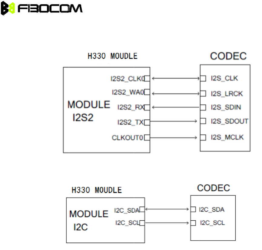
H330 HSPA+
5.8.1 I2S
5.8.2 I2
C
Notice:
(1)
I
(2)
I
K
5.9 Oth
e
Other
a
Module Hard
w
C
I
2S can be
s
I
t support s
o
K
Hz, 11.02
5
e
r
a
re not sup
p
w
are User M
a
s
et master
m
o
me audio s
5
KHz, 8 KH
z
p
orted like
G
a
nual
m
ode of sla
v
ample rate
(
z
).
G
PIO、MIPI
、
v
er mode
(
48KHz, 44.
、
MMC、D
A
1KHz, 32K
H
A
C now.
H
z, 24 KHz,
22.5 KHz,
1
Page 38 of 4
4
1
6 KHz, 12
4

H330 HSPA+
6 Elec
t
6.1 Ele
c
The table i
s
VBAT
Digital Sig
n
6.2 En
v
The table i
s
Operation
a
Temperat
u
Storage
Temperat
u
Module Hard
w
t
rical a
n
c
trical C
h
s
H330 elec
t
n
al
v
ironme
n
s
H330 envi
r
C
a
l
u
re
u
re
w
are User M
a
n
d Envir
h
aracter
t
rical charac
Min.
-0.2
-0.2
n
tal Cha
r
r
onmental c
h
C
ondition
a
nual
onmen
t
istic
teristic:
r
acteristi
h
aracteristi
c
Mi
n
-30
-40
t
al
Max
.
4.2
1.9
c
c
:
n
.
Max.
+85
+85
U
n
V
V
n
it
Unit
°C
°C
Page 39 of 4
4
4
H330 HSPA+
7 RF I
n
H330
m
Main a
n
Diversi
t
7.1 Op
e
7.1.1 Ma
Oper
a
UMT
S
UMT
S
UMT
S
UMT
S
GSM
GSM
GSM
GSM
7.1.2 Di
v
Oper
a
UMT
S
UMT
S
UMT
S
UMT
S
Module Hard
w
n
terfac
e
m
odule incl
u
n
tenna:G
S
t
y antenna:
e
rational
in Antenn
a
ting Band
S
2100 (Ban
S
1900 (Ban
S
850 (Ba
n
S
900 (Ba
n
850 MHz
900
1800(DCS)
1900(PCS)
v
ersity
a
ting Band
S
2100 (Ban
S
1900 (Ban
S
850 (Band
S
900 (Band
w
are User M
a
e
u
des main a
n
S
M/WCDM
A
WCDMA d
Band
a
d I IMT)
d II PCS)
n
d V CLR)
n
d VIII GS
M
d I IMT)
d II PCS)
V CLR)
VIII GSM)
a
nual
n
tenna and
A
Tx and Rx
iversity Rx
.
M
)
diversity an
t
.
.
Tx
1920–19
8
1850–19
1
824–849
M
880–915
824–849
880–915
1710–17
8
1850–19
1
Rx
2110–21
7
1930–19
9
869–894
925–960
t
enna.
8
0 MHz
1
0 MHz
M
Hz
MHz
MHz
8
5 MHz
1
0 MHz
7
0 MHz
9
0 MHz
MHz
MHz
Rx
2110–
2
1930–1
869–8
9
925–9
6
869–8
9
925–9
6
1805–1
1930–1
2
170 MHz
990 MHz
9
4 MHz
6
0 MHz
9
4 MHz
6
0 MHz
880 MHz
990 MHz
Page 40 of 4
4
4
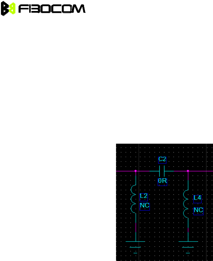
H330 HSPA+
RF PCB
7.1.3 La
y
When desi
g
The shorte
r
It is recom
m
Add a π-ty
p
7.1.4 Im
p
All RF lines
7.2 Ant
e
7.2.1 Ma
1. Anten
n
Antenna ef
f
The radiate
d
losses: retu
dimensions
2. S11 or
S11 (return
impedance
Module Hard
w
Design
y
out Guid
e
g
n RF, we n
e
r
the bette
r
,
i
m
ended to
m
p
e circuit (t
w
p
edance
should be
5
e
nna De
s
in Antenn
n
a Efficien
c
f
iciency is th
d
power of
a
rn loss, ma
t
.
Efficienc
y
VSWR
loss) indica
(50 ohm).
S
w
are User M
a
e
line
e
ed connec
t
i
nsert loss
<
m
ount H330
w
o parallel d
e
5
0ohm imp
e
s
ign
a Design
c
y
e ratio of th
e
a
n antenna
t
erial loss, a
y
of the ma
s
tes the deg
r
S
11 shows t
h
a
nual
t
H330 mod
u
<
0.2dB,an
d
module an
d
e
vice groun
d
e
dance。
Require
m
e
input pow
e
is always lo
w
nd coupling
s
ter antenn
a
r
ee to whic
h
h
e resonanc
u
le RF pin t
o
d
impedanc
e
d
antenna c
o
d
pin directl
y
m
ent
e
r to the ra
d
w
er than th
e
loss. The
e
a
> 40% (–
4
h
the input i
m
e feature a
n
o
antenna,
w
e
is 50ohm.
。
o
nnector to
t
y
to the mai
d
iated or re
c
e
input pow
e
fficiency of
a
4
dB)
m
pedance o
f
n
d impedan
c
w
e recomm
e
。
t
he same si
d
n land) for
a
c
eived powe
er
due to th
e
a
n antenna
f
an antenn
a
c
e bandwidt
h
e
nded to us
e
d
e of layout
a
ntenna ma
t
r o
f
an ante
e
following
a
relates to it
s
a
matches t
h
h
of an ante
Page 41 of 4
4
e
micro-line
.
t
ching.
nna.
a
ntenna
s
electrical
h
e referenc
e
n
na. Voltag
e
4
e
e

H330 HSPA+
standing w
a
be measur
e
S11 o
3. Polari
z
The polariz
a
direction of
The linear
p
antenna 。
4. Radiat
The radiati
o
The radiati
o
PIFA anten
n
A
n
R
a
5. Gain a
The radiati
o
all direction
s
6. Interfe
Besides th
e
(especially
t
sources on
sources, su
interferenc
e
can be dec
r
reduce the
e
LCD with o
p
or design fil
7. TRP/T
I
TRP (
T
Module Hard
w
a
ve ratio (V
S
e
d with vect
o
f the mast
e
z
ation
a
tion of an
a
maximum r
a
p
olarizatio
n
ion Pattern
o
n pattern o
f
o
n pattern o
f
n
a is recom
m
n
tenna area
a
diation P
a
nd Directiv
o
n pattern o
f
s
。
Reco
m
rence
e
antenna p
e
t
he TIS) of t
the user bo
a
ch as the L
C
e
signals th
a
r
eased due
t
e
ffects of in
t
p
timized pe
r
ter circuits.
I
S
T
otal Radiate
d
W850/W
GSM85
0
GSM90
0
DCS180
0
w
are User M
a
S
WR) is an
o
o
r analyzer.
e
r antenna
<
a
ntenna is t
h
a
diation。
n
is recom
m
f
an antenn
a
f
half wave
d
m
ended:
:high
6m
m
a
ttern :o
m
ity
f
an antenn
a
m
mended a
n
e
rformance,
he module.
a
rd must b
e
C
D, CPU, a
u
a
t affect the
t
o interfere
n
t
erference
s
r
formance;
s
d
Power
):
900/W190
0
0
>27dBm
0
>28dBm
0
>25dBm
a
nual
o
the
r
expre
s
<
–10 dB
h
e orientati
o
m
ended fo
r
a
reflects th
e
d
ipole anten
m
*wide 10
m
m
nidirectio
n
a
represent
s
n
tenna gai
n
the interfer
e
To guarant
e
e
properly c
o
u
dio circuit
s
normal ope
r
n
ce signals.
s
ources on t
h
s
hield the L
C
0
/W2100>
1
s
sion of S11
.
o
n of the ele
c
r
the anten
n
e
radiation f
e
nas is the b
e
m
m*long 1
n
al
s
the field st
r
n
≤ 2.5dBi.
e
nce on the
e
e high perf
o
o
ntrolled. O
n
s
, and powe
r
r
ation of the
Therefore,
d
h
e module.
Y
C
D interfere
n
1
9dBm
.
S11 relate
s
c
tric field v
e
n
a:diversi
t
e
atures of t
h
e
st for wirel
e
00mm
。
r
ength of th
e
user board
o
rmance of
n
the user b
o
r
supply. All
module. F
o
d
uring the d
e
Y
ou can ta
k
n
ce signals;
s
to the ant
e
e
ctor that ro
t
t
y antenna
h
e antenna i
n
e
ss termina
e
radiated e
l
also affect
s
the module
,
o
ard, there
a
the interfer
e
o
r example,
t
e
sign, you
n
k
e the follow
shield the
s
e
nna efficie
n
t
ates with ti
m
different t
o
n
the remot
e
ls. If it is bui
l
ectromagn
e
s
the radio p
,
the interfe
r
a
re various
e
nce source
t
he module
n
eed to con
s
ing measur
e
s
ignal cable
Page 42 of 4
4
n
cy. S11 ca
n
m
e in the
o
main
e
field regio
n
lt-in antenn
a
e
tic waves i
n
erformance
r
ence
interferenc
e
s emit
sensitivity
s
ider how t
o
e
s: Use an
of the boar
d
4
n
n
.
a
,
n
e
o
d
;

H330 HSPA+
TIS (
T
o
7.2.2 Di
v
H330 diver
s
Diversity a
n
Main anten
n
EU Reg
Hereby, Sh
e
compliance
Importa
n
The H330
M
H330 Mod
u
conditions.
1. At leas
t
all times.
2. To co
m
radiation, t
h
exceed 2.5
d
3. The H
3
transmitter
o
Module Hard
w
PCS190
0
o
tal Isotropic
W850/W
/W1900/
W
GSM85
0
GSM90
0
DCS180
0
v
ersity an
t
s
ity antenna
n
tenna desi
g
n
a and dive
r
ulatory
C
e
nzhen G&
T
with the es
s
n
t compl
M
odule has
b
u
le in their fi
n
Otherwise,
a
t
20cm sep
a
m
ply with FC
h
e maximu
m
d
Bi.
3
30 Module
o
r antenna
w
w
are User M
a
0
>25dBm
Sensitivity
):
900<-102
d
W
2100<-1
0
0
<-102dB
m
0
<-102dB
m
0
/PCS190
0
t
enna des
i
is optical, I
f
g
n methods
r
sity antenn
a
C
onform
a
T
Industrial
D
s
ential requ
iance in
f
b
een grant
e
n
al product
s
a
dditional F
C
a
ration dist
a
C regulatio
n
m
antenna g
a
and its ant
e
w
ithin a hos
a
nual
d
Bm
0
3dBm;
m
m
0
<-102dB
m
i
gn
f
need to su
and the ma
i
a
isolation r
e
a
nce
D
evelopme
n
irements an
f
ormatio
n
e
d modular
a
s
without ad
d
C
C approv
a
a
nce betwe
e
n
s limiting b
o
a
in includin
g
e
nna must n
o
t device.
m
pport diver
s
i
n antenna,
e
quirement
s
n
t Co., Ltd.,
d other rele
n
for No
r
a
pproval for
d
itional FC
C
a
ls must be
o
e
n the anten
o
th maximu
m
g
cable loss
o
t be co-loc
a
s
ity, must to
its efficienc
y
s
greater th
a
declares th
a
vant provisi
o
r
th Ame
r
mobile app
l
C
certificatio
n
o
btained.
n
a and the
u
m
RF outpu
in a mobile
-
a
ted or ope
r
increase th
e
y
indicators
a
n 12dB.
a
t this mod
u
o
ns of Dire
c
r
ican us
e
l
ications. In
t
n
if they me
e
u
ser’s body
t power an
d
-
only expos
u
r
ating in co
n
e
diversity a
to allow the
u
le, model
H
c
tive 1999/5
/
e
rs
t
egrators m
a
e
t the follo
w
must be m
a
d
human ex
p
u
re conditio
n
n
junction wi
t
Page 43 of 4
4
ntenna.
lower 3dB.
H
330 is in
/
EC.
a
y use the
w
ing
a
intained at
p
osure to R
F
n
must not
t
h any other
4
F

H330 HSPA+
4. A label
with a state
5. A user
that must b
e
The end pr
o
emission te
Note: If this
satisfy the
S
FCC NOTI
C
Changes o
r
Developme
Module Hard
w
must be af
f
ment simila
r
manual wit
h
e
observed
t
o
duct with a
sting requir
e
module is i
n
S
AR require
C
E:
r
modificatio
nt Co., Ltd.
w
are User M
a
f
ixed to the
o
r
to the follo
h
the end pr
o
t
o ensure c
o
n embedde
d
e
ments and
n
tended for
ments of F
C
ns made to
may void th
a
nual
o
utside of t
h
wing: For H
o
duct must
c
o
mpliance
w
d
H330 Mo
d
be properl
y
use in a po
r
C
C Part 2.1
0
this equip
m
e FCC auth
h
e end prod
u
330: This d
e
c
learly indi
c
w
ith current
F
d
ule may al
s
y
authorized
r
table devic
e
0
93.
m
ent not exp
orization to
u
ct into whi
c
e
vice contai
c
ate the ope
r
F
CC RF ex
p
s
o need to p
per FCC P
a
e
, you are r
e
r
essly appr
o
operate thi
s
c
h the H330
ns FCC ID:
r
ating requi
r
p
osure guid
e
ass the FC
C
a
rt 15.
e
sponsible
f
o
ved by Sh
e
s
equipment
Module is i
n
ZMOH330.
r
ements an
d
e
lines.
C
Part 15 u
n
f
or separate
e
nzhen G&
T
.
Page 44 of 4
4
n
corporated
d
conditions
n
intentional
approval t
o
T
Industrial
4
,
o