Fibocom Wireless L816AM LTE module User Manual ng
Fibocom Wireless Inc. LTE module ng
Users Manual

Reproduction forbidden without Fibocom Wireless Inc. written authorization - All Rights Reserved.
L816-AM Hardware User Manual Page
1
of
42
L816-AM Hardware User Manual
Version: 2.0.4
Update date: 2016.09.18

Reproduction forbidden without Fibocom Wireless Inc. written authorization - All Rights Reserved.
L816-AM Hardware User Manual Page
2
of
42
Applicability Table
No.
Product model
Description
1
L816-AM
N/A
Reproduction forbidden without Fibocom Wireless Inc. written authorization - All Rights Reserved.
L816-AM Hardware User Manual Page
3
of
42
Copyright
Copyright © 2016 Fibocom Wireless Inc. All rights reserved.
Without the prior written permission of the copyright holder, any company or individual is prohibited to
excerpt, copy any part of or the entire document, or distribute the document in any form.
Notice
The document is subject to update from time to time owing to the product version upgrade or other
reasons. Unless otherwise specified, the document only serves as the user guide. All the statements,
information and suggestions contained in the document do not constitute any explicit or implicit
guarantee.
Trademark
The trademark is registered and owned by Fibocom Wireless Inc.
Version Record
Version
Update Date
Description
V2.0.0
2016-04-28
Initial version
V2.0.1
2016-07-19
Sections describe modifications
V2.0.2
2016-07-26
Modified description
V2.0.3
2016-07-28
Update part chart
V2.0.4
2016-09-18
Add product certification of warnings

Reproduction forbidden without Fibocom Wireless Inc. written authorization - All Rights Reserved.
L816-AM Hardware User Manual Page
4
of
42
Contents
1 Foreword....................................................................................................................................... 6
1.1 Introduction........................................................................................................................................... 6
1.2 Reference Standard............................................................................................................................ 6
1.3 Related Documents............................................................................................................................. 6
2 Overview........................................................................................................................................7
2.1 Introduction........................................................................................................................................... 7
2.2 Specification..........................................................................................................................................7
2.3 Warnings............................................................................................................................................... 8
2.4 Application Framework..................................................................................................................... 11
2.5 Hardware Framework........................................................................................................................12
3 Application Interface................................................................................................................13
3.1 LGA Interface..................................................................................................................................... 13
3.1.1 Pin Distribution.............................................................................................................................. 13
3.1.2 Pin Definition.................................................................................................................................... 14
3.2 Power Supply..................................................................................................................................... 19
3.2.1 Power Supply................................................................................................................................... 19
3.2.2 Power Consumption........................................................................................................................21
3.3 Control Signal.....................................................................................................................................22
3.3.1 Module Start-up............................................................................................................................... 22
3.3.1.1 Start-up Circuit.............................................................................................................................22
3.3.1.2 Start-up Timing............................................................................................................................ 23
3.3.2 Module Shutdown............................................................................................................................24
3.3.3 Module Reset................................................................................................................................... 25
3.4 USB Interface..................................................................................................................................... 26
3.4.1 USB Interface Definition................................................................................................................. 26
3.4.2 USB Interface Application.............................................................................................................. 26
3.5 USIM Interface................................................................................................................................... 27
3.5.1 USIM Pins......................................................................................................................................... 27
3.5.2 USIM Interface Circuit.....................................................................................................................28
3.5.2.1 N.C. SIM Card Slot..................................................................................................................... 28
3.5.2.2 N.O. SIM Card Slot..................................................................................................................... 28
3.5.3 USIM Hot-Plugging..........................................................................................................................29
3.5.4 USIM Design.................................................................................................................................... 30

Reproduction forbidden without Fibocom Wireless Inc. written authorization - All Rights Reserved.
L816-AM Hardware User Manual Page
5
of
42
3.6 GPIO.................................................................................................................................................... 30
3.6.1 FW_Ready........................................................................................................................................ 31
3.6.2 SMS_Ready......................................................................................................................................31
3.6.3 Wakeup_Host...................................................................................................................................31
3.6.4 PA_Blanking..................................................................................................................................... 32
3.7 Interrupt Control................................................................................................................................. 32
3.7.1 W_Disable#...................................................................................................................................... 32
3.7.2 BodySar.............................................................................................................................................33
3.8 Other Interfaces................................................................................................................................. 33
4 RF Interface................................................................................................................................ 34
4.1 Operating Band.................................................................................................................................. 34
4.2 Transmitting Power............................................................................................................................34
4.3 Receiver Sensitivity........................................................................................................................... 35
4.4 RF PCB Design..................................................................................................................................36
4.4.1 Trace Routing Principle.................................................................................................................. 36
4.4.2 RF Impedance Design.................................................................................................................... 36
4.5 Antenna Design..................................................................................................................................37
4.5.1 Antenna Design Requirements..................................................................................................... 37
5 Structure Specification............................................................................................................38
5.1 Product Appearance..........................................................................................................................38
5.2 Dimension of Structure..................................................................................................................... 39
5.3 Recommended Design for PCB Bonding Pad.............................................................................. 40
5.4 SMT Paster.........................................................................................................................................41
5.5 Storage................................................................................................................................................42
5.5.1 Storage Life...................................................................................................................................... 42
5.5.2 Workshop Life.................................................................................................................................. 42
5.5.3 Recommended baking standards:................................................................................................42
5.6 Packing................................................................................................................................................42
5.6.1 Tray Package....................................................................................................................................42

Reproduction forbidden without Fibocom Wireless Inc. written authorization - All Rights Reserved.
L816-AM Hardware User Manual Page
6
of
42
1 Foreword
1.1 Introduction
The document describes the electrical characteristics, RF performance, dimensions and application
environment, etc. of L816-AM-00 (hereinafter referred to as L816-AM). With the assistance of the
document and other instructions, the developers can quickly understand the hardware functions of
L816-AM modules and develop products.
1.2 Reference Standard
The design of the product complies with the following standards:
3GPP TS 51.010-1 V10.5.0: Mobile Station (MS) conformance specification; Part 1:
Conformance specification
3GPP TS 34.121-1 V10.8.0: User Equipment (UE) conformance specification; Radio
transmission and reception (FDD);Part 1: Conformance specification
3GPP TS 36.521-1 V10.6.0: User Equipment (UE) conformance specification; Radio
transmission and reception; Part 1: Conformance testing
3GPP TS 21.111 V10.0.0: USIM and IC card requirements
3GPP TS 51.011 V4.15.0: Specification of the Subscriber Identity Module -Mobile Equipment
(SIM-ME) interface
3GPP TS 31.102 V10.11.0: Characteristics of the Universal Subscriber Identity Module (USIM)
application
3GPP TS 31.11 V10.16.0: Universal Subscriber Identity Module (USIM) Application
Toolkit(USAT)
3GPP TS 36.124V10.3.0: ElectroMagnetic Compatibility (EMC) requirements for mobile
terminals and ancillary equipment
3GPP TS 27.007 V10.0.8: AT command set for User Equipment (UE)
3GPPTS27.005 V10.0.1: Use of Data Terminal Equipment - Data Circuit terminating Equipment
(DTE - DCE) interface for Short Message Service (SMS) and Cell Broadcast Service (CBS)
1.3 Related Documents
RF Antenna Application Design Specification
FIBOCOM_L8 Family System Driver Integration and Application Guidance
L816-AM AT Commands Manual
L816-AM SMT Application Design Specification
Reproduction forbidden without Fibocom Wireless Inc. written authorization - All Rights Reserved.
L816-AM Hardware User Manual Page
7
of
42
2 Overview
2.1 Introduction
The L816-AM module are highly integrated 4G wireless communication LGA modules, which supports
LTE FDD/WCDMA/GSM systems (3 modes and 7 bands).
2.2 Specification
Specification
Operating Band
LTE FDD: Band II,IV, XII
WCDMA/HSPA+: Band I,II,V(VI),VIII
GSM/GPRS/EDGE: 850/900/1800/1900MHz
Data
Transmission
LTE FDD
Rel.9, 10Mbps DL/5Mbps UL (Cat 1)
WCDMA / HSDPA /
HSUPA:
UMTS:384 kbps DL/384 kbps UL
HSDPA CAT 7:7.2 Mbps Down;HSUPA CAT 6:5.76 Mbps Up
GPRS/EDGE
GPRS:MSC 10, CS-4 80 Kbps Down/20Kbps Up
Power Supply
DC 3.3V~4.5V
Temperature
Operating: -10°C ~+55°C
Storage: -40°C ~+85°C
Physical
characteristics
Package: LGA 115 pins
Dimension:30.0 x 21.0 x 1.55mm
Weight:~2.4g
Interfaces
Antenna
WWAN Main Antenna x 1
WWAN Diversity Antenna x 1
Function
Interface
USIM 3V/1.8V
USB 2.0 x 1
EINT, GPIO
USIM x 1
RF MIPI,RF GPO

Reproduction forbidden without Fibocom Wireless Inc. written authorization - All Rights Reserved.
L816-AM Hardware User Manual Page
8
of
42
Software
AT commands
3GPP TS 27.007 and 27.005, and proprietary FIBOCOM AT commands
Firmware update
USB
2.3 Warnings
2.3.1 CE Statement
EU Regulatory Conformance:
Hereby, We, FIBOCOM Wireless Inc. declares that this device L816-AM is in compliance with the
essential requirements and other relevant provisions of Directive 1999/5/EC.
CE 0560
R&TTE Regulation:
In all cases assessment of the final product must be mass against the Essential requirements of the
R&TTE Directive Articles 3.1(a) and (b), safety and EMC respectively, as well as any relevant Article 3.2
requirements.
The maximum antenna gain for frequency 900 is 3dBi; for frequency 1800 is 5dBi and the antenna
separation distance is 20cm.
2.3.2 FCC Statement
Federal Communication Commission Interference Statement
This device complies with Part 15 of the FCC Rules. Operation is subject to the following two conditions:
(1) This device may not cause harmful interference, and (2) this device must accept any interference
received, including interference that may cause undesired operation.
This equipment has been tested and found to comply with the limits for a Class B digital device, pursuant
to Part 15 of the FCC Rules. These limits are designed to provide reasonable protection against harmful
interference in a residential installation. This equipment generates, uses and can radiate radio frequency
energy and, if not installed and used in accordance with the instructions, may cause harmful interference
to radio communications. However, there is no guarantee that interference will not occur in a particular

Reproduction forbidden without Fibocom Wireless Inc. written authorization - All Rights Reserved.
L816-AM Hardware User Manual Page
9
of
42
installation. If this equipment does cause harmful interference to radio or television reception, which can
be determined by turning the equipment off and on, the user is encouraged to try to correct the
interference by one of the following measures:
Reorient or relocate the receiving antenna.
Increase the separation between the equipment and receiver.
Connect the equipment into an outlet on a circuit different from that
to which the receiver is connected.
Consult the dealer or an experienced radio/TV technician for help.
FCC Caution:
Any changes or modifications not expressly approved by the party responsible for compliance could
void the user's authority to operate this equipment.
This transmitter must not be co-located or operating in conjunction with any other antenna or
transmitter.
Radiation Exposure Statement:
This equipment complies with FCC radiation exposure limits set forth for an uncontrolled environment.
This equipment should be installed and operated with minimum distance 20cm between the radiator &
your body.
This device is intended only for OEM integrators under the following conditions:
1) The antenna must be installed such that 20 cm is maintained between the antenna and
users, and the maximum antenna gain allowed for use with this device is 5dBi.
2) The transmitter module may not be co-located with any other transmitter or antenna.
As long as 2 conditions above are met, further transmitter test will not be required. However, the OEM
integrator is still responsible for testing their end-product for any additional compliance requirements
required with this module installed
IMPORTANT NOTE: In the event that these conditions can not be met (for example certain laptop
configurations or co-location with another transmitter), then the FCC authorization is no longer considered
valid and the FCC ID can not be used on the final product. In these circumstances, the OEM integrator will
be responsible for re-evaluating the end product (including the transmitter) and obtaining a separate FCC
authorization.

Reproduction forbidden without Fibocom Wireless Inc. written authorization - All Rights Reserved.
L816-AM Hardware User Manual Page
10
of
42
End Product Labeling
This transmitter module is authorized only for use in device where the antenna may be installed such that
20 cm may be maintained between the antenna and users. The final end product must be labeled in a
visible area with the following: “Contains FCC ID: ZMOL816AM and IC:21374-L816AM”. The grantee's
FCC ID & IC ID can be used only when all FCC&IC compliance requirements are met.
Manual Information To the End User
The OEM integrator has to be aware not to provide information to the end user regarding how to install or
remove this RF module in the user’s manual of the end product which integrates this module. The end
user manual shall include all required regulatory information/warning as show in this manual.
2.3.3 IC Statement
Industry Canada statement
This device complies with Industry Canada license-exempt RSS standard(s). Operation is subject to
the following two conditions:
1) this device may not cause interference, and
2) this device must accept any interference, including interference that may cause undesired
operation of the device.
Le présent appareil est conforme aux CNR d'Industrie Canada applicables aux appareils radio
exempts de licence. L'exploitation est autorisée aux deux conditions suivantes:
1) l'appareil ne doit pas produire de brouillage, et
2) l'utilisateur de l'appareil doit accepter tout brouillage radioélectrique subi, même si le brouillage
est susceptible d'en compromettre le fonctionnement.
This Class B digital apparatus complies with Canadian ICES-003.
Cet appareil numérique de la classe B est conforme à la norme NMB-003 du Canada.
This device complies with RSS-310 of Industry Canada. Operation is subject to the condition that this
device does not cause harmful interference.
Cet appareil est conforme à la norme RSS-310 d'Industrie Canada. L'opération est soumise à la
condition que cet appareil ne provoque aucune interférence nuisible.
This device and its antenna(s) must not be co-located or operating in conjunction with any other
antenna or transmitter, except tested built-in radios.
Cet appareil et son antenne ne doivent pas être situés ou fonctionner en conjonction avec une autre
antenne ou un autre émetteur, exception faites des radios intégrées qui ont été testées.
The County Code Selection feature is disabled for products marketed in the US/ Canada.
La fonction de sélection de l'indicatif du pays est désactivée pour les produits commercialisés aux
États-Unis et au Canada.
Reproduction forbidden without Fibocom Wireless Inc. written authorization - All Rights Reserved.
L816-AM Hardware User Manual Page
11
of
42
Radiation Exposure Statement:
This equipment complies with IC radiation exposure limits set forth for an uncontrolled environment. This
equipment should be installed and operated with minimum distance 20cm between the radiator & your
body.
Déclaration d'exposition aux radiations:
Cet équipement est conforme aux limites d'exposition aux rayonnements IC établies pour un
environnement non contrôlé. Cet équipement doit être installé et utilisé avec un minimum de 20 cm de
distance entre la source de rayonnement et votre corps.
2.4 Application Framework
The peripheral applications for L816-AM module are shown in Figure 2-1:
Figure2-1 Application Framework
Reproduction forbidden without Fibocom Wireless Inc. written authorization - All Rights Reserved.
L816-AM Hardware User Manual Page
12
of
42
2.5 Hardware Framework
The hardware framework in Figure 2-2 shows the main hardware functions of L816-AM module, including
base band and RF functions.
Baseband contains the followings:
GSM/UMTS/LTE FDD controller/Power supply
NAND+LPDDR2 RAM
Application interface
RF contains the followings:
RF Transceiver
RF Power/PA
RF Front End
RF Filter
Figure 2-2 Hardware Framework
Reproduction forbidden without Fibocom Wireless Inc. written authorization - All Rights Reserved.
L816-AM Hardware User Manual Page
13
of
42
3 Application Interface
3.1 LGA Interface
The L816-AM module applies LGA packaging, with a total of 115 pins.
3.1.1 Pin Distribution
Figure 3-1 Pin Map (TOP Perspective View)

Reproduction forbidden without Fibocom Wireless Inc. written authorization - All Rights Reserved.
L816-AM Hardware User Manual Page
14
of
42
3.1.2 Pin Definition
The L816-AM pin definition is as follows:
Pin
Pin Name
I/O
Reset
Value
Pin Description
Type
USB2.0
13
USB_DP
I/O
T
USB Data Positive
0.3---3V
14
USB_DN
I/O
T
USB Data Negative
0.3---3V
15
VBUS
PI
USB VBUS Supply
2.0---5.25V
SIM
17
SIM1_DATA
I/O
L
USIM data, internal 4.7KΩ pull-up
1.8V/3V
18
SIM1_RST
O
L
USIM reset
1.8V/3V
19
SIM1_CLK
O
L
USIM clock
1.8V/3V
20
VSIM1
PO
USIM power supply
1.8V/3V
26
SIM1_CD
I
USIM card detection with 390KΩ pull-
up, active high
1.8V
EINT
31
Wakeup_Modem
I
PD
Reserved
CMOS 1.8V
40
W_Disable#
I
PD
Disable WWAN
CMOS 1.8V
27
BodySar
I
PD
Body SAR detection
CMOS 1.8V
GPIO
28
FW_Ready
O
PD
FW_Ready output
CMOS 1.8V
29
SMS_Ready
O
PD
SMS_Ready output
CMOS 1.8V
30
USB_En/Disable
O
PD
Enable_Disable-USB Signal Output
CMOS 1.8V
33
PA_Blanking
O
PD
PA_Blanking output
CMOS 1.8V
42
GPIO_Modem
I/O
PD
Reserved
CMOS 1.8V
39
Wakeup_Host
O
PD
Wakeup_Host output
ANT
61
Main_ANT
I/O
Main antenna
68
DIV_ANT
I
Diversity antenna
ANT Tunable

Reproduction forbidden without Fibocom Wireless Inc. written authorization - All Rights Reserved.
L816-AM Hardware User Manual Page
15
of
42
Pin
Pin Name
I/O
Reset
Value
Pin Description
Type
9
RFE_RFFE2_VIO
PO
RFFE2 VIO for tunable ANT
1.8V
10
RFE_RFFE2_SCLK
O
Reserved
1.8V
11
RFE_RFFE2_SDATA
I/O
Reserved
1.8V
RF GPO
4
GPIO_RF1
O
RF_GPIO_1
2.3V
5
GPIO_RF2
O
RF_GPIO_2
2.3V
7
ASM_2V5
PO
ASM_2V5
2.5V
Module Control
32
Reset_N
I
Module reset input with 100KΩ pull-up
1.8V
41
Power_On/Off
I
Module power on/off signal.
Advise the customer to increase the
200KΩ pull-down
1.8V
Power
45
VBAT_BB
PI
-
Power input
Power supply
46
VBAT_PA
PI
-
Power input
Power supply
47
VBAT_PA
PI
-
Power input
Power supply
48
VBAT_TR
PI
-
Power input
Power supply
GND
1
GND
-
-
GND
Ground
2
GND
-
-
GND
Ground
3
GND
-
-
GND
Ground
6
GND
-
-
GND
Ground
8
GND
-
-
GND
Ground
12
GND
-
-
GND
Ground
16
GND
-
-
GND
Ground
21
GND
-
-
GND
Ground
22
GND
-
-
GND
Ground
23
GND
-
-
GND
Ground
24
GND
-
-
GND
Ground

Reproduction forbidden without Fibocom Wireless Inc. written authorization - All Rights Reserved.
L816-AM Hardware User Manual Page
16
of
42
Pin
Pin Name
I/O
Reset
Value
Pin Description
Type
25
GND
-
-
GND
Ground
34
GND
-
-
GND
Ground
35
GND
-
-
GND
Ground
36
GND
-
-
GND
Ground
37
GND
-
-
GND
Ground
38
GND
-
-
GND
Ground
43
GND
-
-
GND
Ground
44
GND
-
-
GND
Ground
49
GND
-
-
GND
Ground
50
GND
-
-
GND
Ground
51
GND
-
-
GND
Ground
52
GND
-
-
GND
Ground
53
GND
-
-
GND
Ground
54
GND
-
-
GND
Ground
55
GND
-
-
GND
Ground
56
GND
-
-
GND
Ground
57
GND
-
-
GND
Ground
58
GND
-
-
GND
Ground
59
GND
-
-
GND
Ground
60
GND
-
-
GND
Ground
62
GND
-
-
GND
Ground
63
GND
-
-
GND
Ground
64
GND
-
-
GND
Ground
65
GND
-
-
GND
Ground
66
GND
-
-
GND
Ground
67
GND
-
-
GND
Ground
69
GND
-
-
GND
Ground
70
GND
-
-
GND
Ground

Reproduction forbidden without Fibocom Wireless Inc. written authorization - All Rights Reserved.
L816-AM Hardware User Manual Page
17
of
42
Pin
Pin Name
I/O
Reset
Value
Pin Description
Type
TG1
GND
-
-
Thermal Ground
Ground
TG2
GND
-
-
Thermal Ground
Ground
TG3
GND
-
-
Thermal Ground
Ground
TG4
GND
-
-
Thermal Ground
Ground
TG5
GND
-
-
Thermal Ground
Ground
TG6
GND
-
-
Thermal Ground
Ground
TG7
GND
-
-
Thermal Ground
Ground
TG8
GND
-
-
Thermal Ground
Ground
TG9
GND
-
-
Thermal Ground
Ground
TG10
GND
-
-
Thermal Ground
Ground
TG11
GND
-
-
Thermal Ground
Ground
TG12
GND
-
-
Thermal Ground
Ground
TG13
GND
-
-
Thermal Ground
Ground
TG14
GND
-
-
Thermal Ground
Ground
TG15
GND
-
-
Thermal Ground
Ground
TG16
GND
-
-
Thermal Ground
Ground
TG17
GND
-
-
Thermal Ground
Ground
TG18
GND
-
-
Thermal Ground
Ground
TG19
GND
-
-
Thermal Ground
Ground
TG20
GND
-
-
Thermal Ground
Ground
TG21
GND
-
-
Thermal Ground
Ground
TG22
GND
-
-
Thermal Ground
Ground
TG23
GND
-
-
Thermal Ground
Ground
TG24
GND
-
-
Thermal Ground
Ground
TG25
GND
-
-
Thermal Ground
Ground
TG26
GND
-
-
Thermal Ground
Ground
TG27
GND
-
-
Thermal Ground
Ground
TG28
GND
-
-
Thermal Ground
Ground
Reproduction forbidden without Fibocom Wireless Inc. written authorization - All Rights Reserved.
L816-AM Hardware User Manual Page
18
of
42
Pin
Pin Name
I/O
Reset
Value
Pin Description
Type
TG29
GND
-
-
Thermal Ground
Ground
TG30
GND
-
-
Thermal Ground
Ground
TG31
GND
-
-
Thermal Ground
Ground
TG32
GND
-
-
Thermal Ground
Ground
TG33
GND
-
-
Thermal Ground
Ground
TG34
GND
-
-
Thermal Ground
Ground
TG35
GND
-
-
Thermal Ground
Ground
TG36
GND
-
-
Thermal Ground
Ground
TG37
GND
-
-
Thermal Ground
Ground
TG38
GND
-
-
Thermal Ground
Ground
TG39
GND
-
-
Thermal Ground
Ground
TG40
GND
-
-
Thermal Ground
Ground
TG41
GND
-
-
Thermal Ground
Ground
TG42
GND
-
-
Thermal Ground
Ground
TG43
GND
-
-
Thermal Ground
Ground
TG44
GND
-
-
Thermal Ground
Ground
TG45
GND
-
-
Thermal Ground
Ground
H: High Voltage Level
L: Low Voltage Level
PD: Pull-Down
PU: Pull-Up
T: Tri-State
OD: Open Drain
PP: Push-Pull
PI: Power Input
PO: Power Output
Note:
The unused pins can be left floating.
Reproduction forbidden without Fibocom Wireless Inc. written authorization - All Rights Reserved.
L816-AM Hardware User Manual Page
19
of
42
3.2 Power Supply
The power interface for L816-AM module is as follows:
Pin
Pin Name
I/O
Pin Description
DC Parameters (V)
Minimum
Value
Typical
Value
Maximum
Value
45
VBAT_BB
PI
Power input to BB
3.3
3.8
4.5
46
VBAT_PA
PI
Power input to RF PA
DC-DC
3.3
3.8
4.5
47
VBAT_PA
PI
Power input to RF PA
DC-DC
3.3
3.8
4.5
48
VBAT_TR
PI
Power input to
transceiver
3.3
3.8
4.5
15
VBUS
PI
USB power supply
2.0
3.8
5.25
20
VSIM1
PO
SIM1 power supply
1.8V/3V
3.2.1 Power Supply
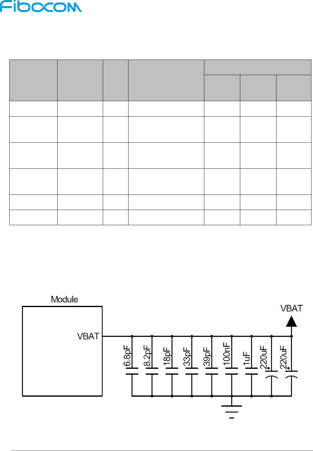
The L816-AM module should be powered through the VBAT pins, and the power supply design is shown
in Figure 3-2:
Figure 3-2 Power Supply Design
Reproduction forbidden without Fibocom Wireless Inc. written authorization - All Rights Reserved.
L816-AM Hardware User Manual Page
20
of
42
The filter capacitor design for power supply is shown in the following table:
Recommended
capacitance
Application
Description
220uF x 2
Voltage-stabilizing capacitors
Reduce power fluctuations of the module in
operation, requiring capacitors with low ESR
LDO or DC/DC power supply requires the
capacitor of no less than 440uF
The capacitor for battery power supply
can be reduced to 100~220uF
1uF,100nF
Digital signal noise
Filter out the interference generated from the
clock and digital signals
39pF,33pF
850/900 MHz frequency band
Filter out low frequency band RF interference
18pF,8.2pF,6.8pF
1800/1900,2100MHz frequency
band
Filter out medium/high frequency band RF
interference
The stable power supply can ensure the normal operation of L816-AM module; and the ripple of the
power supply should be less than 165mV in design. When the module operates under GSM mode (Burst
transmit), the maximum operating current can reach 2A, so the power source should be not lower than
3.135V, or the module may shut down or reboot. The power supply limits are shown in Figure 3-3:
Figure 3-3 Power Supply Limit

Reproduction forbidden without Fibocom Wireless Inc. written authorization - All Rights Reserved.
L816-AM Hardware User Manual Page
21
of
42
3.2.2 Power Consumption
In the case of 3.8V power supply, the power consumption for L816-AM module is shown in the following
table:
Parameter
Mode
Condition
Average
Current(mA)
Ioff
Power off
Power supply, module power off
TBD
IIdle
GPRS
MFRMS=5
TBD
WCDMA
DRX=8
TBD
LTE FDD
DRX=8
TBD
Radio Off
AT+CFUN=4, Flight mode
TBD
ISleep
GPRS
MFRMS=2
TBD
MFRMS=5
TBD
MFRMS=9
TBD
WCDMA
DRX=6
TBD
DRX=8
TBD
DRX=9
TBD
LTE FDD
Paging cycle #64 frames (0.64 sec DRx cycle)
TBD
Radio Off
AT+CFUN=4,Flight mode
TBD
IGPRS-RMS
CS4
GPRS
1Rx slot
nTX slot
GPRS Data transfer GSM850; PCL=5; 1Rx/2Tx
TBD
GPRS Data transfer GSM900; PCL=5; 1Rx/2Tx
TBD
GPRS Data transfer DCS1800; PCL=0; 1Rx/2Tx
TBD
GPRS Data transfer PCS1900; PCL=0; 1Rx/2Tx
TBD
IEGPRS-RMS
MCS9
EDGE
EDGE Data transfer GSM850; PCL=8; 1Rx/2Tx
TBD
EDGE Data transfer GSM900; PCL=8; 1Rx/2Tx
TBD
EDGE Data transfer DCS1800; PCL=2; 1Rx/2Tx
TBD
EDGE Data transfer PCS1900; PCL=2; 1Rx/2Tx
TBD
IWCDMA-RMS
WCDMA
WCDMA Data transfer Band I @+23dBm
TBD
WCDMA Data transfer Band II @+23dBm
TBD

Reproduction forbidden without Fibocom Wireless Inc. written authorization - All Rights Reserved.
L816-AM Hardware User Manual Page
22
of
42
Parameter
Mode
Condition
Average
Current(mA)
WCDMA Data transfer Band V(VI) @+23dBm
TBD
WCDMA Data transfer Band VIII @+23dBm
TBD
ILTE-RMS
LTE FDD
LTE FDD Data transfer Band 2 @+23dBm
TBD
LTE FDD Data transfer Band 4 @+23dBm
TBD
LTE FDD Data transfer Band 12 @+23dBm
TBD
3.3 Control Signal
The L816-AM module provides two control signals to execute the power on/off and reset operations, the
pin definition is as follows:
Pin
Pin Name
I/O
Reset Value
Functions
Type
41
Power_On/Off
I
Power on/off signal with internal 200KΩ
pull-down.
High: Power on
Low or floating: Power off
1.8V
32
Reset_N
I
Reset signal with 100KΩ internal
pull-up, active low.
1.8V
3.3.1 Module Start-up
3.3.1.1 Start-up Circuit
The VRTC output from the module can be used as the pull up voltage and the module has two start-up
modes:
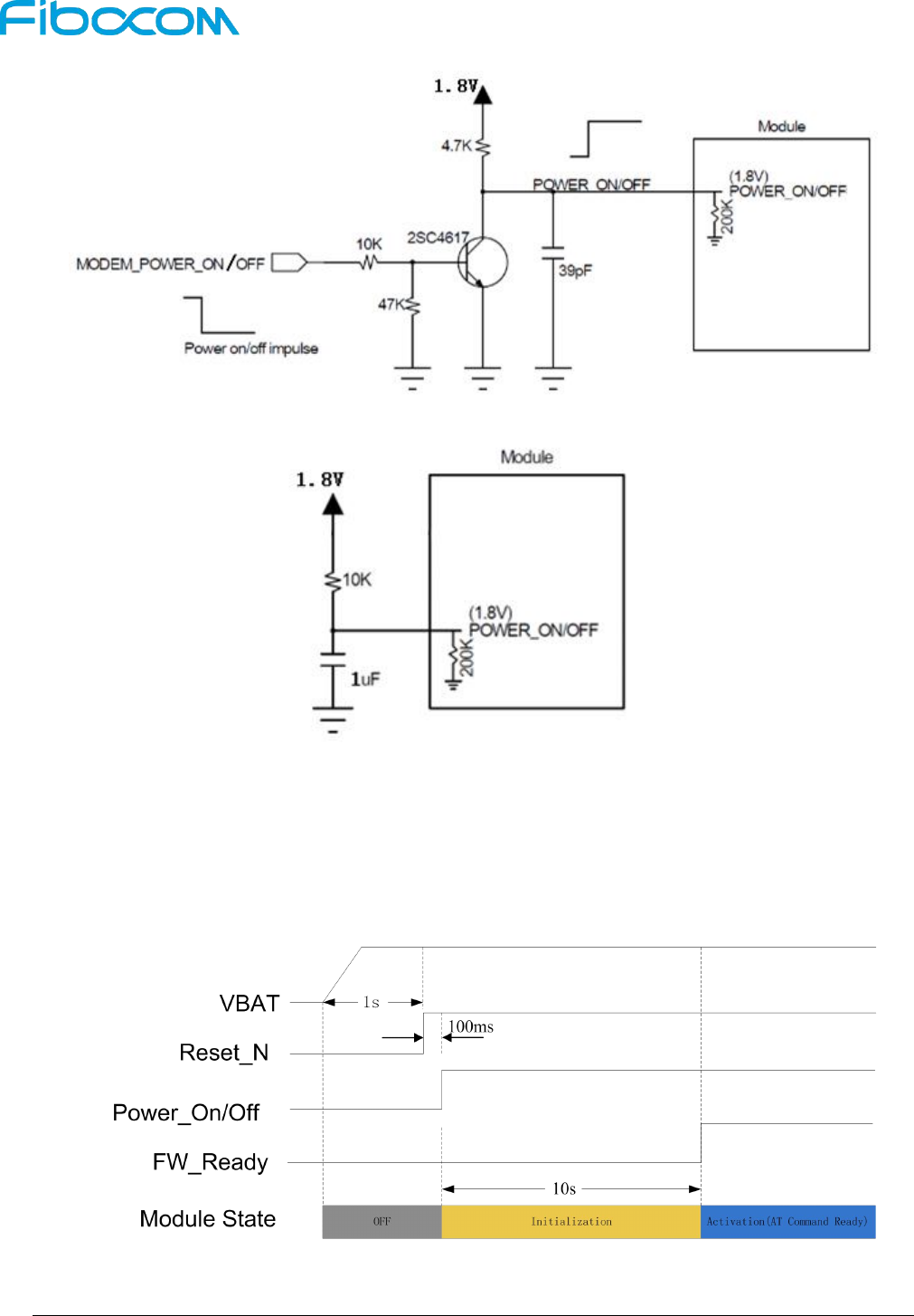
AP (Application Processor) controls the module start-up, and the circuit design is shown in Figure
3-4:
Automatically start-up when powered on, and the circuit design is shown in Figure 3-5:
Reproduction forbidden without Fibocom Wireless Inc. written authorization - All Rights Reserved.
L816-AM Hardware User Manual Page
23
of
42
Figure 3-4 Circuit for Module Start-up Controlled by AP
Figure 3-5 Circuit for Automatic Start-up
3.3.1.2 Start-up Timing
After powering on, the module will start-up by pulling up the Power_On/Off signal for more than 20ms
(100ms is recommended).The start-up timing is shown in Figure 3-6:
Figure 3-6 Timing Control for Start-up
Reproduction forbidden without Fibocom Wireless Inc. written authorization - All Rights Reserved.
L816-AM Hardware User Manual Page
24
of
42
Note:
The Reset_N is required to pull high with a 1s delay after the VBAT, because it takes some time
to charge the capacitors for +3.3V power supply. If the VBAT power supply is already stable
before starting up the module, the delay time can be ignored.
3.3.2 Module Shutdown
The L816-AM module can be shut down by software or hardware control.
Control mode
Action
Condition
Software
Sending AT+CPWROFF
command
Normal shutdown.
Hardware
Pull down Power_On/Off pin
Only used when a hardware exception occurs
and the software control cannot be used.
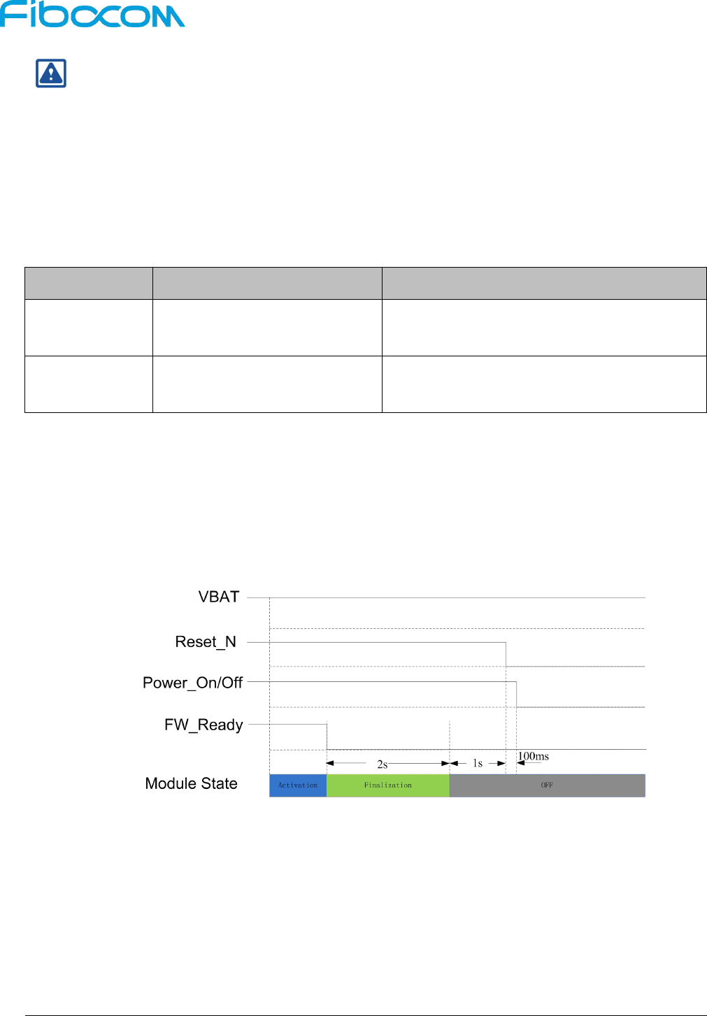
The module can be shut down by sending AT+CPWROFF command. When the module receives the
shutdown command, the module will plug Low the FW_Ready and start the finalization process (the
reverse process of initialization), and it will be completed after 3s. In the finalization process, the module
will save the network, SIM card and some other parameters from memory, then clear the memory and
PMU will be powered off. The control timing is shown in Figure 3-7:
Figure 3-7 Software Shutdown Timing Control
After the software shutdown, the Power_On/Off pin will remain high which prevents the module from
restarting again. To enable the next restart, the Power_On/Off pin should be pulled low after shutting
down.
Reproduction forbidden without Fibocom Wireless Inc. written authorization - All Rights Reserved.
L816-AM Hardware User Manual Page
25
of
42
3.3.3 Module Reset
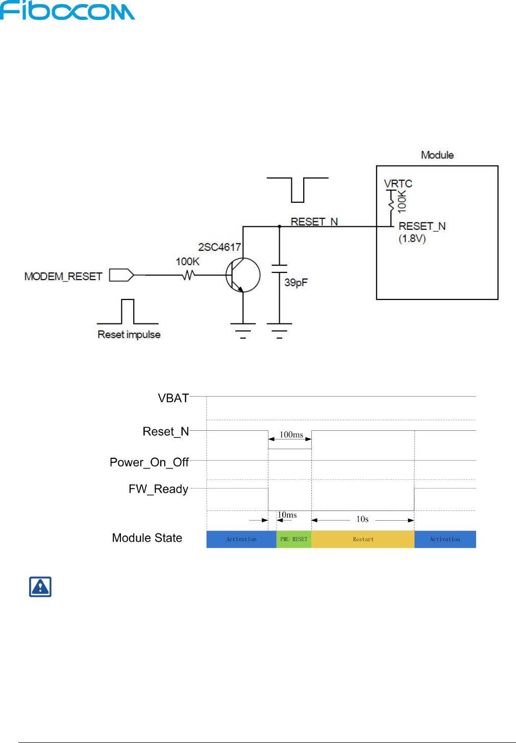
The L816-AM module can reset to its initial status by pulling down the Reset_N signal for more than 10ms
(100ms is recommended), and the module will restart after the Reset_N signal is released. When the
customer executes Reset_N function, the PMU remains its power inside the module. The recommended
circuit design is shown in the Figure 3-8:
Figure 3-8 Recommended Design for Reset Circuit
The reset control timing is shown in Figure 3-9:
Figure 3-9 Reset Timing Control
Note:
Reset_N is a sensitive signal, it’s recommended to add a filter capacitor close to the module. In
case of PCB layout, the Reset_N signal lines should keep away from the RF interference and
protected by GND. Also, the Reset_N signal lines shall neither near the PCB edge nor route on
the surface planes to avoid module from reset caused by ESD problems.
Reproduction forbidden without Fibocom Wireless Inc. written authorization - All Rights Reserved.
L816-AM Hardware User Manual Page
26
of
42
3.4 USB Interface
The L816-AM module supports USB 2.0 which is compatible with USB High-Speed (480 Mbit/s) and USB
Full-Speed (12 Mbit/s). For the USB timing and electrical specification of L816-AM module, please refer to
“Universal Serial Bus Specification 2.0”.
3.4.1 USB Interface Definition
Pin
Pin Name
I/O
Reset Value
Pin Description
Type
15
VBUS
PI
USB power supply
2.0---5.25V
14
USB_DN
IO
T
USB Data Negative
0.3---3V
13
USB_DP
IO
T
USB Data Positive
0.3---3V
The VBUS power supply is used as the detection of the USB port; after VBUS is powered on, the USB
function of the module will be enabled and the enumeration will begin. The VBUS pin is only used for the
detection of USB port, and the supply current is about 1mA. When USB_DN & USB_DP are disconnected,
the module will not enter sleep mode for the case if VBUS power is supplied.
The USB driver will map 3 COM ports and 4 NCM ports, which are described as follows:
2 COM ports are used to send AT Commands.
1 COM port is used to capture LOG information with debugging softwares.
4 NCM ports are virtual network ports, which are used to initiate the data service.
Note:
One COM port can be used as the Modem COM port to initiate the data service. Since the speed
of the Modem COM port is not sufficient for the 150 Mbps peak downlink speed requirement for
LTE, so it is not recommended to be used.
3.4.2 USB Interface Application
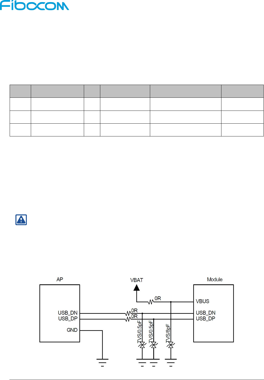
The reference circuit is shown in Figure 3-10:
Figure 3-10 Reference Circuit for USB Interface

Reproduction forbidden without Fibocom Wireless Inc. written authorization - All Rights Reserved.
L816-AM Hardware User Manual Page
27
of
42
Since the module supports USB 2.0 High-Speed, it is required to use TVS diodes with equivalent
capacitance of 1pF or smaller ones on the USB_DN/DP differential signal lines, it is recommended to use
0.5pF TVS diodes. There is no special requirement for TVS diodes on VBUS pin, normally the 8 ~ 10pF
TVS diodes can be used.
USB_DN and USB_DP are high speed differential signal lines with the maximum transfer rate of 480
Mbit/s, so the following rules shall be followed carefully in the case of PCB layout:
USB_DN and USB_DP signal lines should have the differential impedance of 90 ohms.
USB_DN and USB_DP signal lines should be parallel and have the equal length, the right angle
routing should be avoided.
USB_DN and USB_DP signal lines should be routed on the layer that is next to the ground layer,
and be wrapped with GND on both sides and layers.
3.5 USIM Interface
The L816-AM module has a built-in USIM card interface, which supports 1.8V and 3V SIM cards.
3.5.1 USIM Pins
The USIM pins are described as follows:
Pin
Pin Name
I/O
Reset Value
Pin Description
Type
20
VSIM1
PO
USIM power supply
1.8V/3V
18
SIM1_RST
O
L
USIM reset
1.8V/3V
19
SIM1_CLK
O
L
USIM clock
1.8V/3V
17
SIM1_DATA
I/O
L
USIM data with internal 4.7KΩ pull-up
1.8V/3V
26
SIM1_CD
I
USIM card detection with 390KΩ pull up.
Active-high, and high level means SIM
card is inserted; and low level means SIM
card is detached.
1.8V
Reproduction forbidden without Fibocom Wireless Inc. written authorization - All Rights Reserved.
L816-AM Hardware User Manual Page
28
of
42
3.5.2 USIM Interface Circuit
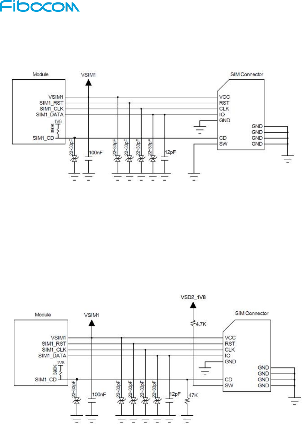
3.5.2.1 N.C. SIM Card Slot
The reference circuit design for N.C. (Normally Closed) SIM card slot is shown in Figure 3-11:
Figure 3-11 Reference Circuit for N.C. SIM Card Slot
The principles for N.C. SIM card slot design are described as follows:
When the SIM card is detached, it connects the short circuit between CD and SW pins, and drives the
SIM1_CD pin low.
When the SIM card is inserted, it connects an open circuit between CD and SW pins, and drives the
SIM1_CD pin high.
Suggested SIM1_CD pin increase TVS to protect the pin.
3.5.2.2 N.O. SIM Card Slot
The reference circuit design for N.O. (Normally Open) SIM card slot is shown in Figure 3-12:
Figure 3-12 Reference Circuit for N.O. SIM Card Slot

Reproduction forbidden without Fibocom Wireless Inc. written authorization - All Rights Reserved.
L816-AM Hardware User Manual Page
29
of
42
The principles for N.O. SIM card slot design are described as follows:
When the SIM card is detached, it connects an open circuit between CD and SW pins, and drives the
SIM1_CD pin low.
When the SIM card is inserted, it connects the short circuit between CD and SW pins, and drives the
SIM1_CD pin high.
Suggested SIM1_CD pin increase TVS to protect the pin.
3.5.3 USIM Hot-Plugging
The L816-AM module supports the SIM card hot-plugging detection function, which determines whether
the SIM card is inserted or detached by detecting the SIM1_CD pin state of the SIM card slot.
The SIM card hot-plugging detection function can be configured by “AT+MSMPD” command, and the
description for AT command is as follows:
AT Command
Hot-plugging Detection
Function Description
AT+MSMPD=1
Enable
Default value, the SIM card hot-plugging detection
function is enabled.
The module can detect whether the SIM card is inserted
or not through the SIM1_CD pin state.
AT+MSMPD=0
Disable
The SIM card hot-plugging detection function is disabled.
The module reads the SIM card when starting up, and the
SIM1_CD status will not be detected.
After the SIM card hot-plugging detection function is enabled, the module detects that the SIM card is
inserted when the SIM1_CD pin is high, then executes the initialization program and finish the network
registration after reading the SIM card information. When the SIM1_CD pin is low, the module determines
that the SIM card is detached and does not read the SIM card.
Note:
By default, SIM1_CD is active-high, which can be switched to active-low by the AT command.
Please refer to the AT Commands Manual for the AT command.

Reproduction forbidden without Fibocom Wireless Inc. written authorization - All Rights Reserved.
L816-AM Hardware User Manual Page
30
of
42
3.5.4 USIM Design
The SIM card circuit design shall meet the EMC standards and ESD requirements with the improved
capability to resist interference, to ensure that the SIM card can work stably. The following guidelines
should be noted in case of design:
The SIM card slot placement should near the module as close as possible, and away from the
RF antenna, DC/DC power supply, clock signal lines, and other strong interference sources.
The SIM card slot with a metal shielding housing can improve the anti-interference ability.
The trace length between the SIM card slot and the module should not exceed 100mm, or it
could reduce the signal quality.
The SIM1_CLK and SIM1_DATA signal lines should be isolated by GND to avoid crosstalk
interference. If it is difficult for the layout, the whole SIM signal lines should be wrapped with
GND as a group at least.
The filter capacitors and ESD devices for SIM card signals should be placed near to the SIM
card slot, and the ESD devices with 22~33pF capacitance should be used.
3.6 GPIO
The L816-AM module provides four signals to indicate the operating status of the module, the status
indicator pins are as follows:
Pin
Pin Name
I/O
Reset Value
Pin Description
Type
28
FW_Ready
O
PD
Modem SMS Ready Inform
HOST 1.8V
CMOS 1.8V
29
SMS_Ready
O
PD
Modem FW Ready Inform
HOST 1.8V
CMOS 1.8V
30
USB_En/Disable
O
PD
Reserved
CMOS 1.8V
39
Wakeup_Host
O
PD
Module wakes up Host (AP).
CMOS 1.8V
33
PA_Blanking
O
PD
PA Blanking output, external
GPS control signal.
CMOS 1.8V
42
GPIO_Modem
O
PD
Reserved
CMOS 1.8V
Reproduction forbidden without Fibocom Wireless Inc. written authorization - All Rights Reserved.
L816-AM Hardware User Manual Page
31
of
42
3.6.1 FW_Ready
Firmware ready is a modem driven GPIO, which on power on reset, it should be low. Once the firmware in
the modem is ready after boot, it should assert (high) GPIO. In an unlikely event of a firmware/modem
crash, if a crash/exception handler is to be run, FW ready GPIO should be de-asserted.
FW_Ready timing is shown in Figure 3-6,3-7,3-9。
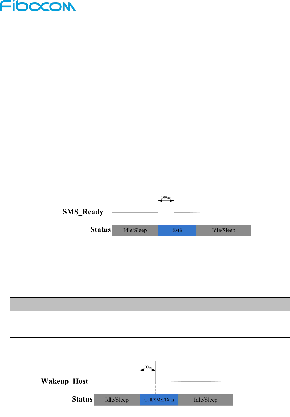
3.6.2 SMS_Ready
SMS ready is a modem driven GPIO, which should be low while power up/off and reset sequences.
Whenever modem receives an SMS from the network, it should assert (high) GPIO during 100msec, then
de-assert (low).
SMS ready GPIO should be triggered by non-class 2 “SIM card data” messages regardless message
storage status (even the storage is full and not be able to store new received message).
SMS_Ready timing is shown in Figure 3-13:
Figure 3-13 SMS_Ready Timing
3.6.3 Wakeup_Host
The Wakeup_Host signal is used to wake the Host (AP) when there is an incoming call, SMS or other data
requests. The definition of Wakeup_Host signal is as follows:
Operating Mode
Wakeup_Host Signal
Ringing /SMS or data requests
Pull high 100ms then pull low (pulse signal).
Idle/Sleep
low level
Wakeup_Host timing is shown in Figure 3-14:
Figure 3-14 Wakeup_Host Timing
Reproduction forbidden without Fibocom Wireless Inc. written authorization - All Rights Reserved.
L816-AM Hardware User Manual Page
32
of
42
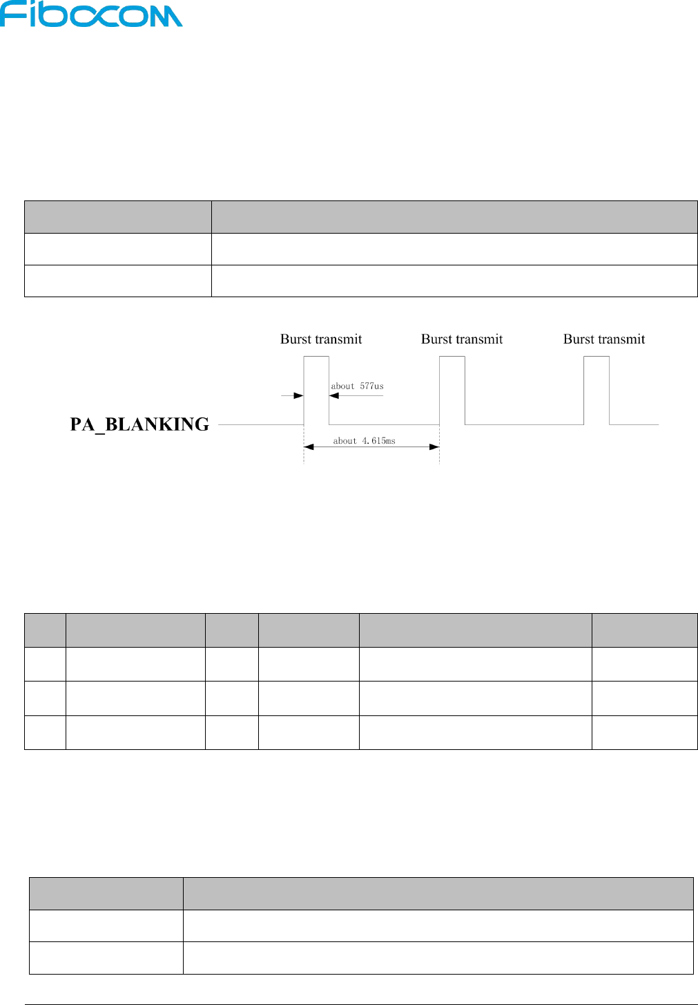
3.6.4 PA_Blanking
While the module works in GSM frequency band, the PA_Blanking pin will output the pulse signals that
synchronize with the GSM burst TX timing. As the GSM TX may interfere the receiving of the GPS signal,
AP can disable GPS or stop receiving GPS data when it detects the PA_Blanking pulse signals, to avoid
GPS working abnormally.
Operating modes
PA_BLANKING signal
Default
Low level
GSM burst TX
Output the pulse signals that synchronize with the GSM burst TX.
PA_BLANKING timing is shown in Figure 3-15:
Figure 3-15 PA_Blanking Timing
3.7 Interrupt Control
The L816-AM module provides four interrupt signals, and the pin definition is as follows:
Pin
Pin Name
I/O
Reset Value
Pin Description
Type
31
Wakeup_Modem
I
PD
Reserved
CMOS 1.8V
40
W_Disable#
I
PD
Enable/Disable RF network
CMOS 1.8V
27
BodySar
I
PU
Body SAR detection
CMOS 1.8V
3.7.1 W_Disable#
The module provides a hardware pin to enable/disable WWAN RF function, and the function can also be
controlled by the AT command. The module enters the Flight mode after the RF function is disabled. The
definition of W_Disable# signal is as follows:
W_Disable# signal
Function
High/Floating
WWAN enable, the module exits the Flight mode.
Low
WWAN disable, the module enters Flight mode.
Reproduction forbidden without Fibocom Wireless Inc. written authorization - All Rights Reserved.
L816-AM Hardware User Manual Page
33
of
42
3.7.2 BodySar
The L816-AM module supports the BodySar detection function. The voltage level is high by default for
BodySar, and when the SAR sensor detects the closing human body, the BodySar signal will be pulled
down. As the result, the module then lowers down its emission power to its default threshold value, thus
reducing the RF radiation on the human body. The threshold of emission power can be set by the AT
Commands. The definition for BodySar function is as follows:
BodySar signal
Function
High/Floating
The module keeps the default emission power.
Low
Lower the maximum emission power to the threshold value of the module.
3.8 Other Interfaces
ANT Tunable, and RF_GPO.
Pin
Pin Name
I/O
Reset Value
Pin Description
Type
9
RFE_RFFE2_VIO
PO
PD
RF LOGIC SWITCH
1.8V
10
RFE_RFFE2_SCLK
O
PD
Reserved
1.8V
11
RFE_RFFE2_SDATA
I/O
PD
Reserved
1.8V
Pin
Pin Name
I/O
Reset Value
Pin Description
Type
4
GPIO_RF1
O
PD
RF LOGIC SWITCH
2.3V
5
GPIO_RF2
O
PD
RF LOGIC SWITCH
2.3V
The RFFE port will be re-purposed to be GPO, with GPO1/GPO2, they can be used control external
DPDT, SPxT.

Reproduction forbidden without Fibocom Wireless Inc. written authorization - All Rights Reserved.
L816-AM Hardware User Manual Page
34
of
42
4 RF Interface
4.1 Operating Band
The L816-AM module provides main and diversity antenna interfaces; main antenna is used to transmit
and receive RF signals, and the diversity antenna is only used to receive RF signals. The operating bands
of the antennas are as follows:
Operating
Band
Description
Mode
Tx (MHz)
Rx (MHz)
Band 1
IMT 2100MHz
WCDMA
1920 - 1980
2110 - 2170
Band 2
PCS 1900MHz
LTE FDD/WCDMA/GSM
1850 - 1910
1930 - 1990
Band 3
DCS 1800MHz
GSM
1710 - 1785
1805 - 1880
Band 4
AWS 1700MHz
LTE FDD
1710 - 1755
2110 - 2155
Band 5
CLR 850MHz
WCDMA/GSM
824 - 849
869 - 894
Band 6
850MHz
WCDMA
830 - 840
875 -885
Band 8
E-GSM 900MHz
WCDMA/GSM
880 - 915
925 - 960
Band 12
Lower SMH/LSMH
blocks A/B/C
LTE FDD
699 - 716
729 - 746
4.2 Transmitting Power
The transmitting power for each band of the L816-AM module is as follows:
Mode
Band
Tx Power(dBm)
Note
GPRS
(1 slot Tx)
GSM850
32.5±1dBm
GSM900
32.5±1dBm
DCS1800
29.5±1dBm
PCS1900
29.5±1dBm
WCDMA
Band I
23±1dBm
Band II
23±1dBm
Band V
23±1dBm
Band VI
23±1dBm
Reproduction forbidden without Fibocom Wireless Inc. written authorization - All Rights Reserved.
L816-AM Hardware User Manual Page
35
of
42
Mode
Band
Tx Power(dBm)
Note
Band VIII
23±1dBm
LTE FDD
Band 2
23±1dBm
10MHz Bandwidth, 1 RB
Band 4
23±1dBm
10MHz Bandwidth, 1 RB
Band 12
23±1dBm
10MHz Bandwidth, 1 RB
4.3 Receiver Sensitivity
The receiver sensitivity for each band of the L816-AM module is as follows:
Mode
Band
Rx Sensitivity(dbm)-typical
Note
GPRS
GSM850
TBD
BLER<10%
GSM900
TBD
BLER<10%
DCS1800
TBD
BLER<10%
PCS1900
TBD
BLER<10%
WCDMA
Band I
TBD
BER<0.1%
Band II
TBD
BER<0.1%
Band V
TBD
BER<0.1%
Band VI
TBD
BER<0.1%
Band VIII
TBD
BER<0.1%
LTE FDD
Band 2
TBD
10MHz Bandwidth
Band 4
TBD
10MHz Bandwidth
Band 12
TBD
10MHz Bandwidth
Note:
The above LTE values are measured for the Dual-Antenna situation (Main + Diversity). For
single main antenna (without Diversity), the sensitivity will drop around 3dBm for each band of
LTE. The WCDMA and GSM have not diversity function.
Reproduction forbidden without Fibocom Wireless Inc. written authorization - All Rights Reserved.
L816-AM Hardware User Manual Page
36
of
42
4.4 RF PCB Design
4.4.1 Trace Routing Principle
The L816-AM module supports dual antennas, which meets the requirements for LTE of 3GPP. The
MAIN_ANT is used to transmit and receive RF signals, while the DIV_ANT is used to receive RF signals.
Using diversity antenna to improve the receiving sensitivity of RF antenna and double the download rate.
Since L816-AM is an LTE module, dual antennas should be applied to meet the performance
requirements.
The L816-AM module does not provide RF connector itself, so routing RF traces are required for the
connection with RF connectors or antenna feed points on the application mainboard. It is recommended
to use the microstrip line for RF trace, with the insertion loss controlled within 0.2dB and impedance
controlled at 50Ω.
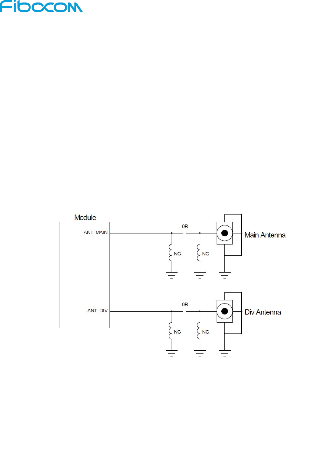
It is recommended to reserve a π circuit (the parallel inductors should connect to the RF trace) between
the L816-AM module and the antenna connectors (or the feed points). The parallel devices are directly
across the RF lines and no branch is allowed.
Figure 4-1 L816-AM Antenna π Circuit
4.4.2 RF Impedance Design
The RF traces impedance of the antenna interface shall be controlled at 50Ω.

Reproduction forbidden without Fibocom Wireless Inc. written authorization - All Rights Reserved.
L816-AM Hardware User Manual Page
37
of
42
4.5 Antenna Design
4.5.1 Antenna Design Requirements
The L816-AM module provides Main and Diversity antenna interfaces, and the antenna design
requirements are as follows:
Main antenna requirements for L816-AM module
Frequency range
The most proper antenna to adapt the frequencies should be used.
Bandwidth
(GPRS/EDGE)
GSM850 : 70 MHz
GSM900 : 80 MHz
GSM1800(DCS) : 170 MHz
GSM1900(PCS) : 140 MHz
Bandwidth (WCDMA)
WCDMA band I(2100) : 250 MHz
WCDMA band II(1900) : 140 MHz
WCDMA band V(850) : 70 MHz
WCDMA band VI(850): 55MHz
WCDMA band VIII(900) : 80 MHz
Bandwidth (LTE)
LTE band 2(1900): 140 MHz
LTE Band 4(1700): 445 MHz
LTE band 12(700): 50 MHz
Impedance
50 Ohm
Input power
> 35dBm(2W) peak power GSM
> 25dBm average power WCDMA & LTE
Recommended
standing-wave ratio
(SWR)
≤ 2:1
Reproduction forbidden without Fibocom Wireless Inc. written authorization - All Rights Reserved.
L816-AM Hardware User Manual Page
38
of
42
5 Structure Specification
5.1 Product Appearance
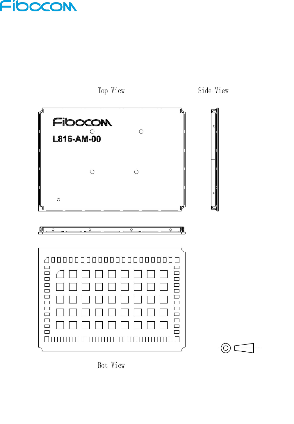
The product appearance for L816-AM module is shown in Figure 5-1:
Figure 5-1 Module Appearance
Reproduction forbidden without Fibocom Wireless Inc. written authorization - All Rights Reserved.
L816-AM Hardware User Manual Page
39
of
42
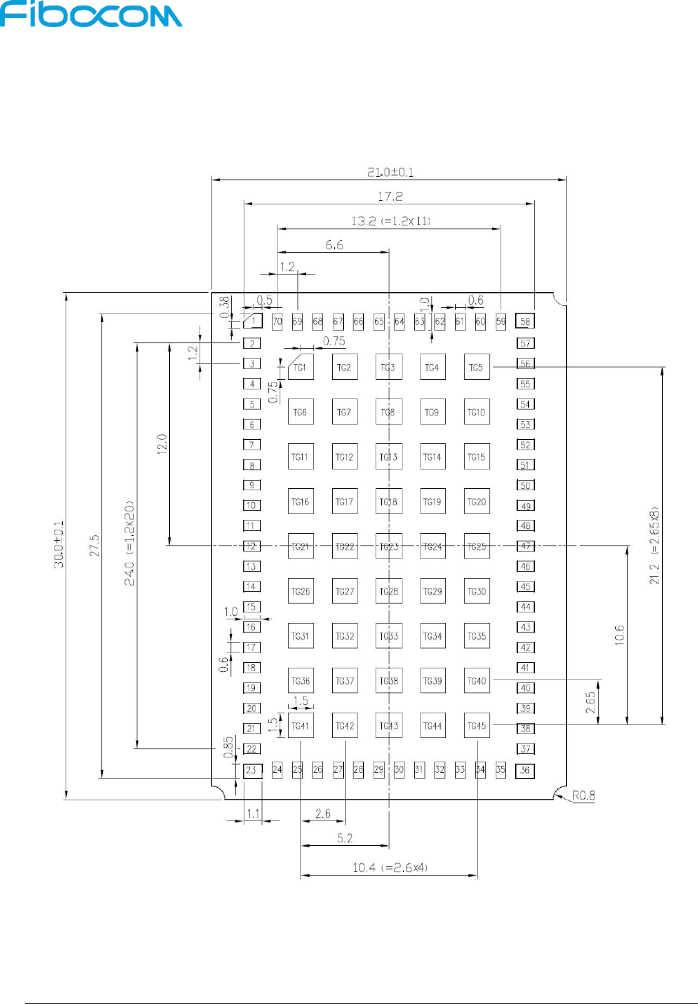
5.2 Dimension of Structure
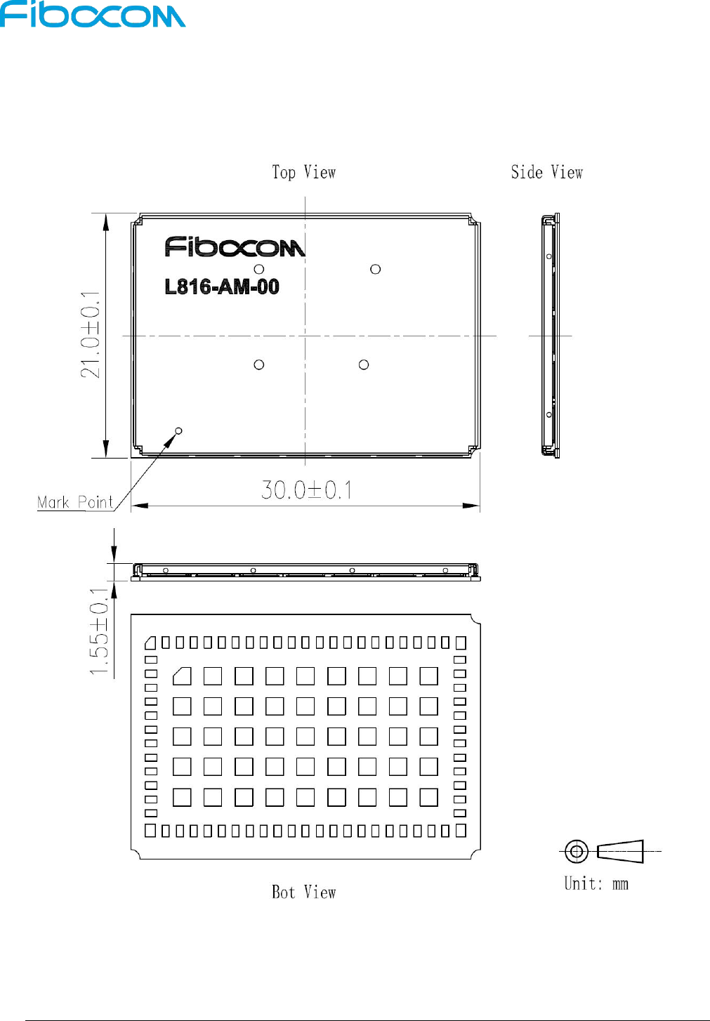
The structural dimension of the L816-AM module is shown in Figure 5-2:
Figure 5-2 Dimension of Structure
Reproduction forbidden without Fibocom Wireless Inc. written authorization - All Rights Reserved.
L816-AM Hardware User Manual Page
40
of
42
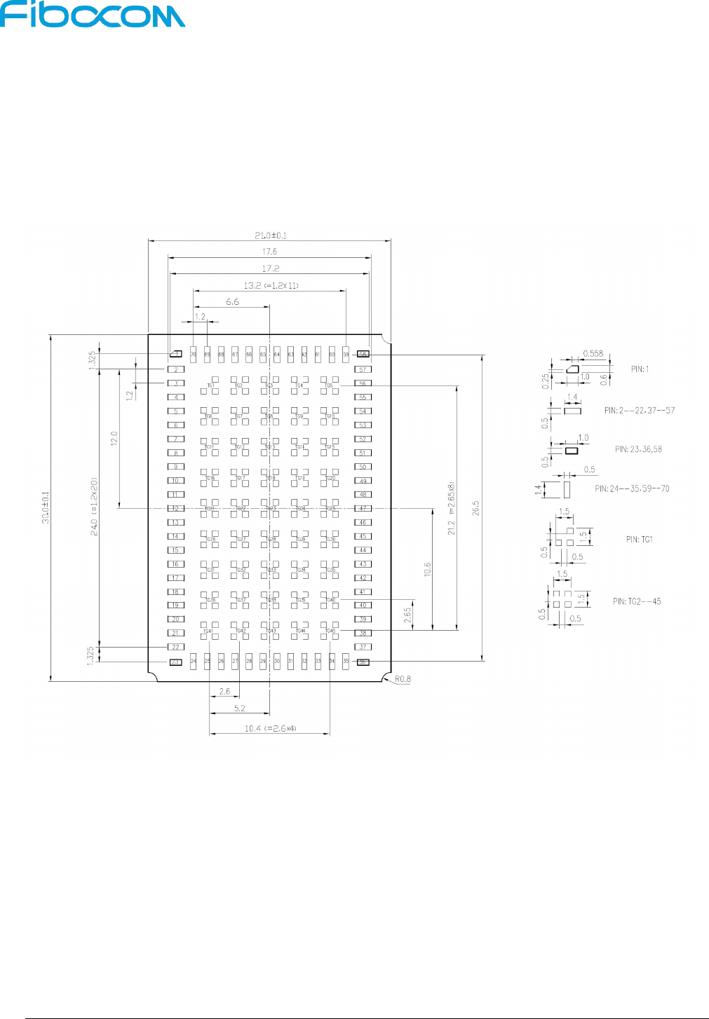
5.3 Recommended Design for PCB Bonding Pad
Recommended Design for PCB Bonding Pad of the L816-AM module is shown in Figure 5-3
Figure5-3 Recommended Design for PCB Bonding Pad (Unit: mm)
Reproduction forbidden without Fibocom Wireless Inc. written authorization - All Rights Reserved.
L816-AM Hardware User Manual Page
41
of
42
5.4 SMT Paster
SMT Paster of the L816-AM module is shown in Figure Figure5-4
Please refer to L816-AM SMT Application Design Specification
Stencil thickness≥0.12mm
Figure5-4 Recommended Design for stencil (Unit: mm)

Reproduction forbidden without Fibocom Wireless Inc. written authorization - All Rights Reserved.
L816-AM Hardware User Manual Page
42
of
42
5.5 Storage
5.5.1 Storage Life
Storage Conditions (recommended): Temperature is 23 ± 5 ℃, relative humidity is RH 35-70%.
Storage period (sealed vacuum packing): Under the recommended storage conditions, the storage life is
12 months.
5.5.2 Workshop Life
For the module integrated some components for “Class 3” humidity-sensitive ,the workshop life need
24hours. After unpacking and under the environment with the room temperature of 23±5 ℃and the
relative humidity of less than 60%, the reflow production or other high-temperature operations shall be
conducted within 24 hours for products, or products shall be stored in the environment with the relative
humidity of less than 10%, in order to keep products dry.
5.5.3 Recommended baking standards:
Continuous baking time: 24 hours.
Temperature: 125±5℃.
Oven: Heat convection oven.
Component tray can NOT be baked on high temperature, Need use high temperature tray baking
5.6 Packing
The L816-AM module uses the tray sealed vacuum packing, combined with the outer packing method
using the hard cartoon box, so that the storage, transportation and the usage of modules can be protected
to the greatest extent.
Note:
The vacuum package bag includes the humidity card and a desiccant. The module is the
humidity sensitive device, and the humidity sensitivity level is Class 3, which meets the
requirements of the American Electronic Component Industry Association (JEDEC). Please read
the relevant application guidance and precautions referred to herein, to avoid the permanent
damage to the product caused by humidity.
5.6.1 Tray Package
Please read the L816-AM packing instructions of Fibocom company 《FIBOCOM-SAL-WI-63 L816-AM Packing
Instruction A0》.