Flir BelgiumBA AX905 WiFi and Bluetooth module User Manual
Raymarine UK Ltd. WiFi and Bluetooth module
Contents
- 1. User manual
- 2. User manual statements
User manual
AMPAK
CONFIDENTIAL
保存期限:最新版本 C-RD-047A
正基科技股份有限公司
SPECIFICATION
SPEC. NO.: REV: 1.4
DATE: 01.08. 2016
PRODUCT NAME: AP6212
Customer APPROVED
Company
Representative
Signature
REVIEW
PREPARED PM QA
APPROVED DCC ISSUE
SPEC-W-014
Beth
Anna
Carol
Richard
2016.01.20
AMPAK
D.C.C PUBLISH

AMPAK
CONFIDENTIAL
保存期限:最新版本 C-RD-047A
AMPAK
AP6212
WiFi+Bluetooth 4.0+FM RX
SIP Module Spec Sheet

AMPAK
CONFIDENTIAL
保存期限:最新版本 C-RD-047A
1
Revision History
Date Revision Content Revised By Version
2014/04/08 - Preliminary Brian 1.0
2014/09/02 - Pin Definition Modified Brian 1.1
2014/11/26 - Bluetooth Spec Modified Brian 1.2
2014/12/26 - Add Process Brian 1.3
2016/01/08 - Add Reflow Suggestion and MLS Beth 1.4

AMPAK
CONFIDENTIAL
保存期限:最新版本 C-RD-047A
2
Contents
Contents ................................................................................................................... 2
1. Introduction......................................................................................................... 3
2. Features............................................................................................................... 4
3. Deliverables ........................................................................................................ 5
3.1 Deliverables.................................................................................................... 5
3.2 Regulatory certifications ................................................................................. 5
4. General Specification......................................................................................... 6
4.1 General Specification...................................................................................... 6
4.2 Voltages.......................................................................................................... 6
4.2.1 Absolute Maximum Ratings.................................................................... 6
4.2.2 Recommended Operating Rating ........................................................... 6
5. WiFi RF Specification......................................................................................... 7
5.1 2.4GHz RF Specification................................................................................. 7
6. Bluetooth Specification...................................................................................... 9
6.1 Bluetooth Specification ................................................................................... 9
7. FM Specification............................................................................................... 10
7.1 FM Specification (TBD)................................................................................. 10
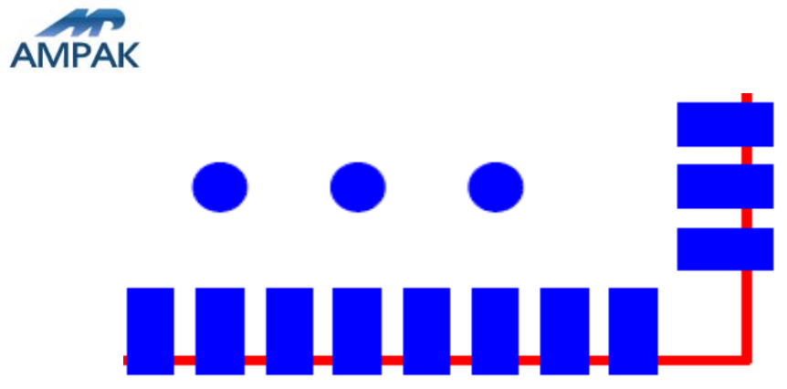
8. Pin Assignments............................................................................................... 11
8.1 Pin Outline .................................................................................................... 11
8.2 Pin Definition ................................................................................................ 11
9. Dimensions ....................................................................................................... 13
9.1 Physical Dimensions..................................................................................... 13
9.2 Layout Recommendation.............................................................................. 14
10. External clock reference .................................................................................. 15
10.1 SDIO Pin Description.................................................................................. 15
11. Host Interface Timing Diagramo...................................................................... 16
11.1 Power-up Sequence Timing Diagram ......................................................... 16
11.2 SDIO Default Mode Timing Diagram........................................................... 18
11.3 SDIO High Speed Mode Timing Diagram.................................................... 19
12. Recommended Reflow Profile......................................................................... 20
Solder Paste definition.......................................................................................... 21
13. Package Information........................................................................................ 23
13.1Label .......................................................................................................... 23
Label C Inner box label . .................................................................................... 23
Label D Carton box label . ................................................................................. 23
13.2 Dimension ................................................................................................. 24
13.3 MSL Level / Storage Condition ................................................................... 26

AMPAK
CONFIDENTIAL
保存期限:最新版本 C-RD-047A
3
1. Introduction
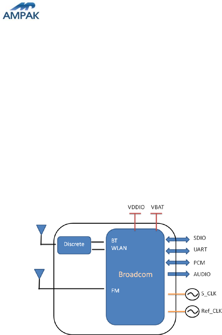
AMPAK Technology would like to announce a low-cost and low-power consumption module
which has all of the WiFi, Bluetooth and FM functionalities. The highly integrated module
makes the possibilities of web browsing, VoIP, Bluetooth headsets, FM radio functional
applications and other applications. With seamless roaming capabilities and advanced
security, also could interact with different vendors’ 802.11b/g/n Access Points in the wireless
LAN.
The wireless module complies with IEEE 802.11 b/g/n standard and it can achieve up to a
speed of 72.2Mbps with single stream in 802.11n draft, 54Mbps as specified in IEEE
802.11g, or 11Mbps for IEEE 802.11b to connect to the wireless LAN. The integrated
module provides SDIO interface for WiFi, UART / I2S / PCM interface for Bluetooth and
UART / I2S / PCM interface for FM.
This compact module is a total solution for a combination of WiFi + BT + FM technologies.
The module is specifically developed for Smart phones and Portable devices.
AMPAK
CONFIDENTIAL
保存期限:最新版本 C-RD-047A
4
2. Features
802.11b/g/n single-band radio
Bluetooth V4.0(HS) with integrated Class 1.5 PA and Low Energy (BLE) support
Concurrent Bluetooth, FM (RX) RDS/RBDS, and WLAN operation
Simultaneous BT/WLAN receive with single antenna
WLAN host interface options:
- SDIO v2.0 — up to 50 MHz clock rate
BT host digital interface:
- UART (up to 4 Mbps)
FM multiple audio routing options: I2S, PCM, eSCO, A2DP
IEEE Co-existence technologies are integrated die solution
ECI — enhanced coexistence support, ability to coordinate BT SCO transmissions
around WLAN receives
A simplified block diagram of the module is depicted in the figure below.

AMPAK
CONFIDENTIAL
保存期限:最新版本 C-RD-047A
5
3. Deliverables
3.1 Deliverables
The following products and software will be part of the product.
Module with packaging
Evaluation Kits
Software utility for integration, performance test.
Product Datasheet.
Agency certified pre-tested report with the adapter board.
3.2 Regulatory certifications
The product delivery is a pre-tested module, without the module level certification.
For module approval, the platform’s antennas are required for the certification.
AMPAK
CONFIDENTIAL
保存期限:最新版本 C-RD-047A
6
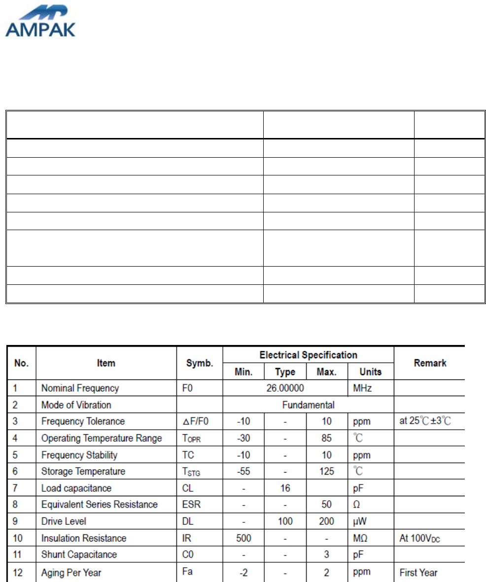
4. General Specification
4.1 General Specification
4.2 Voltages
4.2.1 Absolute Maximum Ratings
Symbol Description Min. Max. Unit
VBAT Input supply Voltage -0.5 5.5 V
WL_VIO_SD Digital/Bluetooth/SDIO/ I/O Voltage -0.5 3.6 V
4.2.2 Recommended Operating Rating
The module requires two power supplies: VBAT and VDDIO.
Min. Typ. Max. Unit
Operating Temperature -30 25 85 deg.C
VBAT 3.0 3.6 4.8 V
VDDIO 1.7 3.3 3.6 V
Model Name AP6212
Product Description Support WiFi/Bluetooth/FM functionalities
Dimension L x W x H: 12 x 12 x 1.5 (typical) mm
WiFi Interface SDIOV2.0
BT Interface UART / PCM
FM Interface UART / PCM / Audio
Operating temperature -30°C to 85°C
Storage temperature -40°C to 85°C
Humidity Operating Humidity 10% to 95% Non-Condensing
AMPAK
CONFIDENTIAL
保存期限:最新版本 C-RD-047A
7
5. WiFi RF Specification
5.1 2.4GHz RF Specification
Conditions : VBAT=3.6V ; VDDIO=3.3V ; Temp:25°C
Feature Description
WLAN Standard IEEE 802.11b/g/n, WiFi compliant
Frequency Range 2.400 GHz ~ 2.497 GHz (2.4 GHz ISM Band)
Number of Channels 2.4GHz:Ch1 ~ Ch14
Modulation 802.11b : DQPSK, DBPSK, CCK
802.11 g/n : OFDM /64-QAM,16-QAM, QPSK, BPSK
802.11b /11Mbps : 16 dBm ± 1.5 dB @ EVM -9dB
802.11g /54Mbps : 15 dBm ± 1.5 dB @ EVM -25dB
Output Power
802.11n /65Mbps : 14 dBm ± 1.5 dB @ EVM -28dB
- MCS=0 PER @ -85 dBm, typical
- MCS=1 PER @ -84 dBm, typical
- MCS=2 PER @ -82 dBm, typical
- MCS=3 PER @ -80 dBm, typical
- MCS=4 PER @ -77 dBm, typical
- MCS=5 PER @ -73 dBm, typical
- MCS=6 PER @ -71 dBm, typical
Receive Sensitivity
(11n,20MHz)
@10% PER
- MCS=7 PER @ -68 dBm, typical
- 6Mbps PER @ -86 dBm, typical
- 9Mbps PER @ -85 dBm, typical
- 12Mbps PER @ -85 dBm, typical
- 18Mbps PER @ -83 dBm, typical
- 24Mbps PER @ -81 dBm, typical
- 36Mbps PER @ -78 dBm, typical
- 48Mbps PER @ -73 dBm, typical
Receive Sensitivity (11g)
@10% PER
- 54Mbps PER @ -71 dBm, typical
- 1Mbps PER @ -90 dBm, typical
- 2Mbps PER @ -88 dBm, typical
- 5.5Mbps PER @ -87 dBm, typical
Receive Sensitivity (11b)
@8% PER
- 11Mbps PER @ -84 dBm, typical
802.11b : 1, 2, 5.5, 11Mbps
Data Rate 802.11g : 6, 9, 12, 18, 24, 36, 48, 54Mbps

AMPAK
CONFIDENTIAL
保存期限:最新版本 C-RD-047A
8
Data Rate
(20MHz ,Long GI,800ns)
802.11n: 6.5, 13, 19.5, 26, 39, 52, 58.5, 65Mbps
Data Rate
(20MHz ,short GI,400ns)
802.11n : 7.2, 14.4, 21.7, 28.9, 43.3, 57.8, 65,72.2Mbps
802.11b : -10 dBm
Maximum Input Level 802.11g/n : -20 dBm
Antenna Reference Small antennas with 0~2 dBi peak gain
AMPAK
CONFIDENTIAL
保存期限:最新版本 C-RD-047A
9
6. Bluetooth Specification
6.1 Bluetooth Specification
Conditions : VBAT=3.6V ; VDDIO=3.3V ; Temp:25°C
Feature Description
General Specification
Bluetooth Standard Bluetooth V4.0 of 1, 2 and 3 Mbps.
Host Interface UART
Antenna Reference Small antennas with 0~2 dBi peak gain
Frequency Band 2402MHz ~ 2480MHz
Number of Channels 79 channels
Modulation FHSS, GFSK, DPSK, DQPSK
RF Specification
Min. Typical. Max.
Output Power (Class 1.5) 9 dBm
Sensitivity @ BER=0.1%
for GFSK (1Mbps) -86 dBm
Sensitivity @ BER=0.01%
for π/4-DQPSK (2Mbps) -86 dBm
Sensitivity @ BER=0.01%
for 8DPSK (3Mbps) -80 dBm
GFSK (1Mbps):-20dBm
π/4-DQPSK (2Mbps) :-20dBm
Maximum Input Level
8DPSK (3Mbps) :-20dBm
AMPAK
CONFIDENTIAL
保存期限:最新版本 C-RD-047A
10
7. FM Specification
7.1 FM Specification (TBD)
Conditions : VBAT=3.6V ; VDDIO=3.3V ; Temp:25°C
Feature Description
General Specification
Frequency Band 76MHz-108MHz
Host Interface HCI UART, I2S/PCM
Channel step 50 KHz
Analog Audio output load RL>30KΩ, CL>20pF
Characteristics Condition MIN TYP MAX UNIT
Output Power Level dBuV
Audio harmonic distortion
(fmod=1KHz, △f=75KHz,
Pilot △f=6.75KHz)
%
MONO
Transmitter
(FM Tx load = 120nH,
Q>30) Audio SNR
(△f=22.5KHz, I2S
audio in SNR ≧
57dB ) Stereo
dB
RDS Sensitivity dBm
fmod=
1KHz Audio harmonic
distortion
(Vin=1mV, △f=75KHz) fmod=
3KHz
%
MONO
Maximum SNR
△
(fmod=1KHz, f=22.5
KHz, BW=300Hz to
15KHz)
Stereo
dB
Receiver
(FM Tx Antenna =
120nH, Q>30)
RF input power level dBuV
AMPAK
CONFIDENTIAL
保存期限:最新版本 C-RD-047A
11
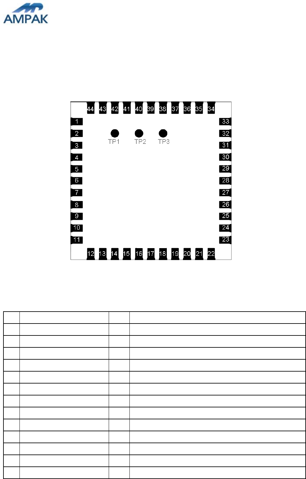
8. Pin Assignments
8.1 Pin Outline
< TOP VIEW >
8.2 Pin Definition
NO Name Type Description
1 GND - Ground connections
2 WL_BT_ANT I/O RF I/O port
3 GND - Ground connections
4 FM_RX I FM radio RF input antenna port
5 NC - Floating (Don’t connected to ground)
6 BT_WAKE I HOST wake-up Bluetooth device
7 BT_HOST_WAKE O Bluetooth device to wake-up HOST
8 NC - Floating (Don’t connected to ground)
9 VBAT P Main power voltage source input
10 XTAL_IN I Crystal input
11 XTAL_OUT O Crystal output
12 WL_REG_ON I Internal regulators power enable/disable
13 WL_HOST_WAKE O WLAN to wake-up HOST

AMPAK
CONFIDENTIAL
保存期限:最新版本 C-RD-047A
12
14 SDIO_DATA_2 I/O SDIO data line 2
15 SDIO_DATA_3 I/O SDIO data line 3
16 SDIO_DATA_CMD I/O SDIO command line
17 SDIO_DATA_CLK I/O SDIO clock line
18 SDIO_DATA_0 I/O SDIO data line 0
19 SDIO_DATA_1 I/O SDIO data line 1
20 GND - Ground connections
21 VIN_LDO_OUT P Internal Buck voltage generation pin
22 VDDIO P I/O Voltage supply input
23 VIN_LDO P Internal Buck voltage generation pin
24 LPO I External Low Power Clock input (32.768KHz)
25 PCM_OUT O PCM Data output
26 PCM_CLK I/O PCM clock
27 PCM_IN I PCM data input
28 PCM_SYNC I/O PCM sync signal
29 NC - Floating (Don’t connected to ground)
30 NC - Floating (Don’t connected to ground)
31 GND - Ground connections
32 NC - Floating (Don’t connected to ground)
33 GND - Ground connections
34 BT_RST_N I Low asserting reset for Bluetooth core
35 NC - Floating (Don’t connected to ground)
36 GND - Ground connections
37 GPIO4 I/O WiFi Co-existence pin with LTE
38 GPIO3 I/O WiFi Co-existence pin with LTE
39 GPIO2 I/O WiFi Co-existence pin with LTE
40 GPIO1 I/O WiFi Co-existence pin with LTE
41 UART_RTS_N O Bluetooth/FM UART interface
42 UART_TXD O Bluetooth/FM UART interface
43 UART_RXD I Bluetooth/FM UART interface
44 UART_CTS_N I Bluetooth/FM UART interface
45 TP1 O FM Analog AUDIO left output
46 TP2 O FM Analog AUDIO right output
47 TP3 (NC) - Floating (Don’t connected to ground)
AMPAK
CONFIDENTIAL
保存期限:最新版本 C-RD-047A
13
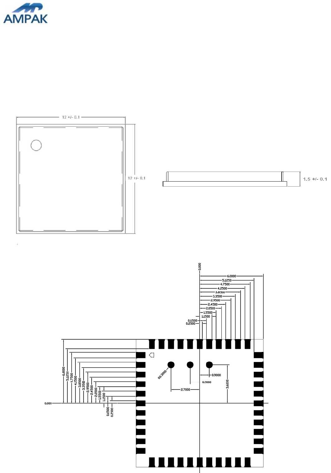
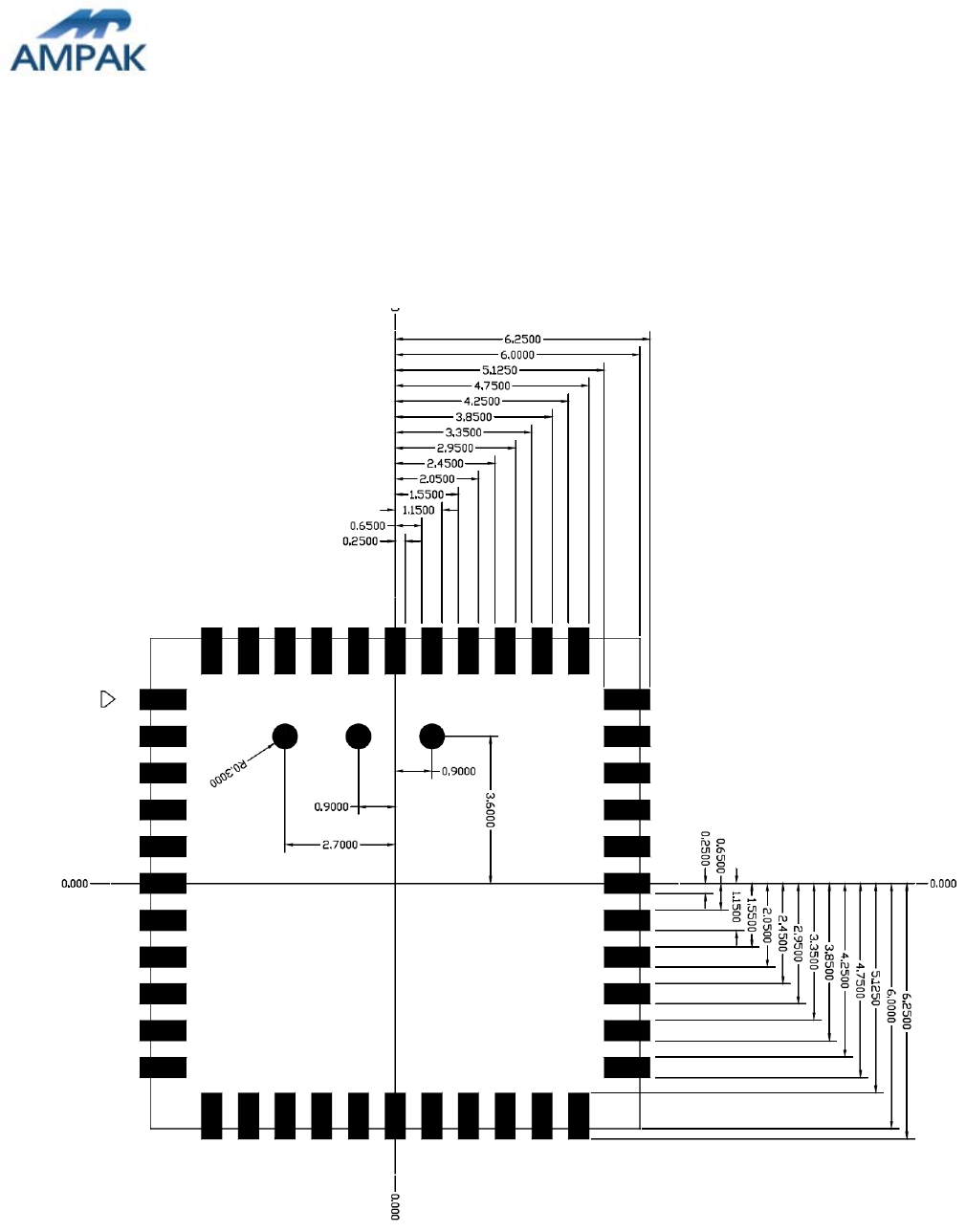
9. Dimensions
9.1 Physical Dimensions
(Unit: mm)
< TOP VIEW > < Side View >
< TOP VIEW >
AMPAK
CONFIDENTIAL
保存期限:最新版本 C-RD-047A
14
9.2 Layout Recommendation
(Unit: mm)
< TOP VIEW >
AMPAK
CONFIDENTIAL
保存期限:最新版本 C-RD-047A
15
10. External clock reference
External LPO signal characteristics
Parameter Specification Units
Nominal input frequency 32.768 kHz
Frequency accuracy 30
ppm
Duty cycle 30 - 70 %
Input signal amplitude 400 to 1800 mV, p-p
Signal type Square-wave -
Input impedance >100k
<5
pF
Clock jitter (integrated over 300Hz – 15KHz) <1 Hz
Output high voltage 0.7Vio - Vio V
External Ref_CLK signal characteristics
10.1 SDIO Pin Description
The module supports SDIO version 2.0 for 4-bit modes (100 Mbps), and high speed 4-bit (50
MHz clocks – 200 Mbps). It has the ability to stop the SDIO clock and map the interrupt
signal into a GPIO pin. This ‘out-of-band’ interrupt signal notifies the host when the WLAN
device wants to turn on the SDIO interface. The ability to force the control of the gated
clocks from within the WLAN chip is also provided.
AMPAK
CONFIDENTIAL
保存期限:最新版本 C-RD-047A
16
Function 0 Standard SDIO function (Max BlockSize / ByteCount = 32B)
Function 1 Backplane Function to access the internal System On Chip (SOC)
address space (Max BlockSize / ByteCount = 64B)
Function 2 WLAN Function for efficient WLAN packet transfer through DMA (Max
BlockSize/ByteCount=512B)
SDIO Pin Description
SD 4-Bit Mode
DATA0 Data Line 0
DATA1 Data Line 1 or Interrupt
DATA2 Data Line 2 or Read Wait
DATA3 Data Line 3
CLK Clock
CMD Command Line
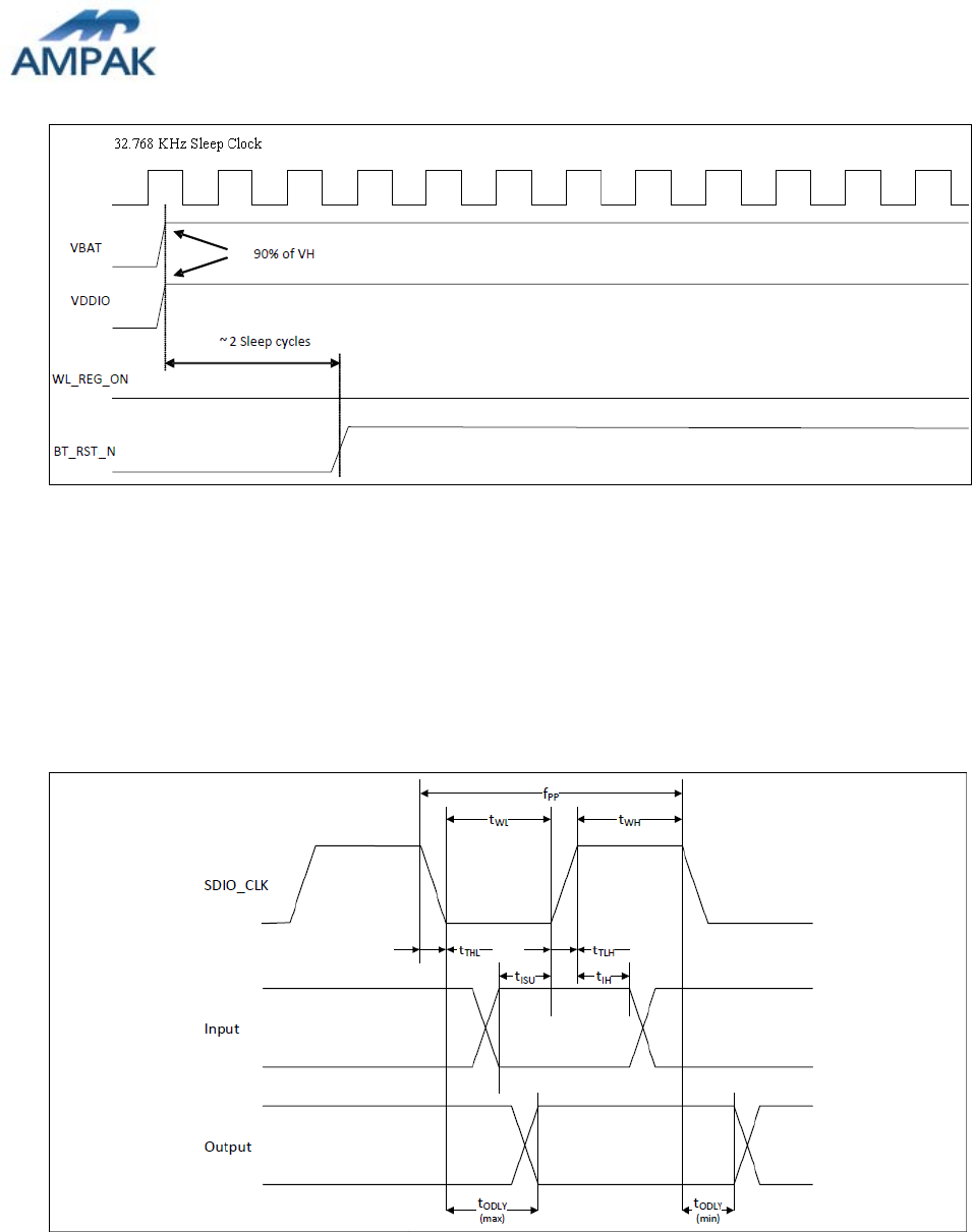
11. Host Interface Timing Diagram
11.1 Power-up Sequence Timing Diagram
The module has signals that allow the host to control power consumption by enabling or
disabling the Bluetooth, WLAN and internal regulator blocks. These signals are described
below.
Additionally, diagrams are provided to indicate proper sequencing of the signals for carious
operating states. The timing value indicated are minimum required values: longer delays are
also acceptable.
※ WL_REG_ON: Used by the PMU to power up the WLAN section. When this pin is
high, the regulators are enabled and the WLAN section is out of reset. When this
pin is low the WLAN section is in reset.
※ BT_RST_N: Low asserting reset for Bluetooth and FM only. This pin has no effect
on WLAN and does not control any PMU functions. This pin must be driven high or
low (not left floating).
AMPAK
CONFIDENTIAL
保存期限:最新版本 C-RD-047A
17
WLAN=ON, Bluetooth=ON
WLAN=OFF, Bluetooth=OFF
WLAN=ON, Bluetooth=OFF
AMPAK
CONFIDENTIAL
保存期限:最新版本 C-RD-047A
18
WLAN=OFF, Bluetooth=ON
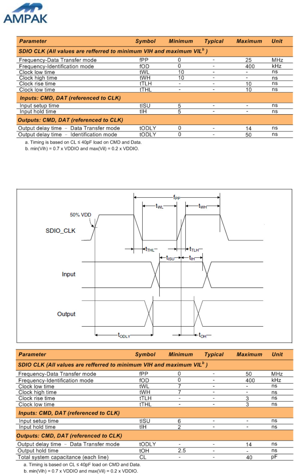
11.2 SDIO Default Mode Timing Diagram
AMPAK
CONFIDENTIAL
保存期限:最新版本 C-RD-047A
19
11.3 SDIO High Speed Mode Timing Diagram
AMPAK
CONFIDENTIAL
保存期限:最新版本 C-RD-047A
20
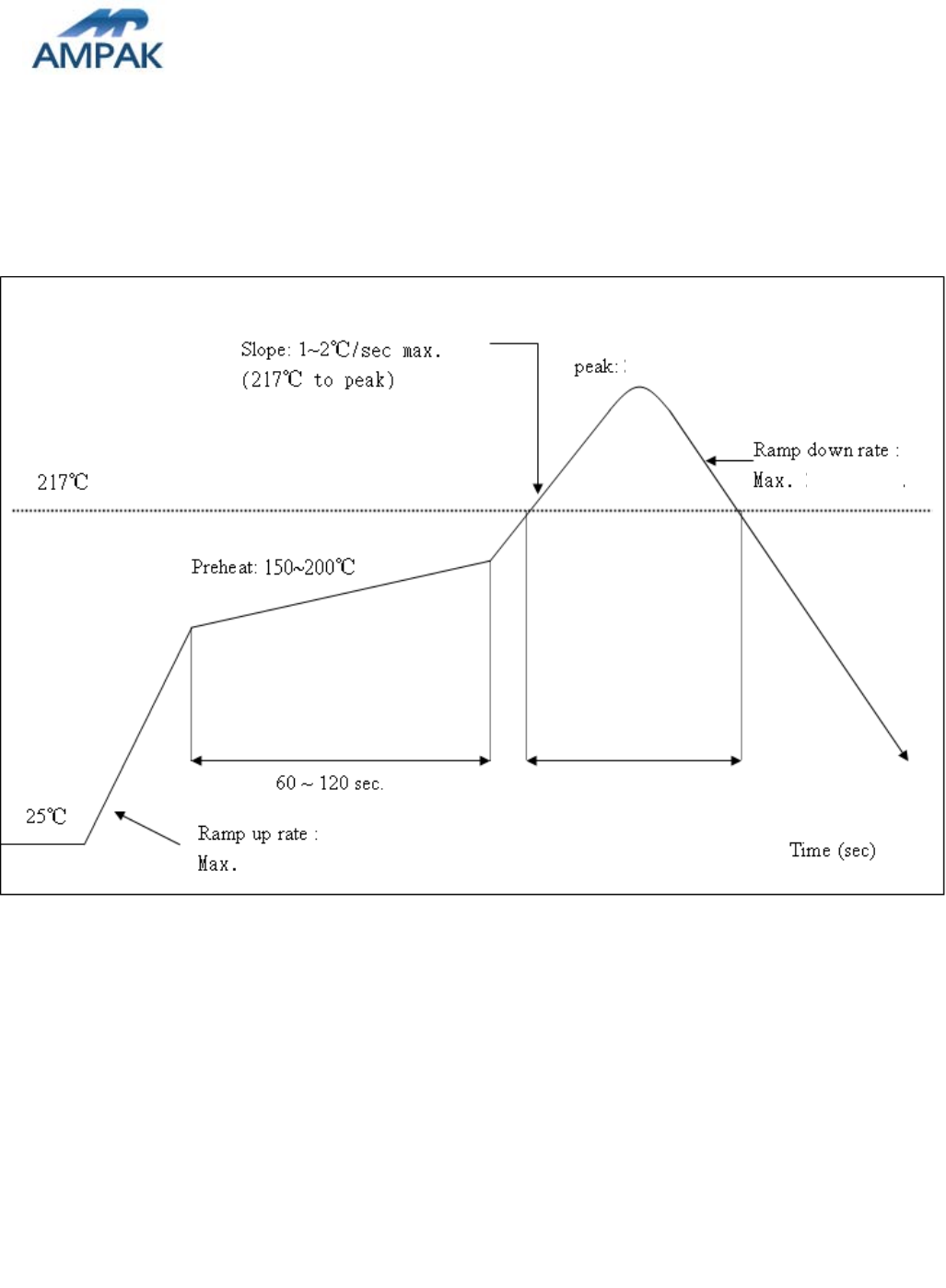
12. Recommended Reflow Profile
Referred to IPC/JEDEC standard.
Peak Temperature : <250°C
Number of Times : 2 times
2.5 /sec℃
2.5°C
/
sec
40~70 sec
250℃
ThenotificationofWiFimodulebeforemounting:
Theapertureofstencilshouldbelargerthanfootprintofmodule,andthestencilthicknessshould
benotlessthan0.12mm.
Reflow 時需使用 N2, 含氧量建議 5000 ppm 以下,
ItmustuseN2forreflowandsuggesttheconcentrationofoxygenlessthan5000ppm.
AMPAK
CONFIDENTIAL
保存期限:最新版本 C-RD-047A
21
Solder Paste definition
Module Specifications : W:0.65mm * L:0.95mm pitch 0.9 mm
The proposed design W:0.65~0.75 mm * L:1.33mm. Consider not place other parts in
the peripheral area of 1 mm ~ 1.5 mm to facilitate additional amount of solder for PCB
pad.
We Suggest the thickness of Stencil between 0.12 mm ~0.15mm, the W between
0.6~0.65mm and the L between L1.5~1.6mm.
If the thickness of the stencil is thinner, we suggest to adding more solder, to increase
the wetting ability. Depends on different production situation, if the stencil thickness is
0.08~0.1mm, and the module nearby area is no more space for expending soldering
area, we will suggest to increase the stencil thickness to increase the wetting ability.
The major consideration parts of stencil design is to increase the solder paste wetting
ability.
模組規格 W0.65mm *L0.95mm Pitch 0.9mm
PCB Pad建議設計 W0.65~0.75mm *L1.33mm,
且周邊1mm~1.5mm區域考慮不放置零件以利外
加錫量。
鋼網建議厚度為0.12mm~0.15mm,
W0.6~0.65mm* L1.5~1.6mm
因為模組需要側面爬錫,當鋼網厚度越薄外加錫量
需越多,需依實際生產狀態評估,當使用鋼網
0.08mm或 0.1mm且外加可能性低時則必須考慮
局部加厚鋼網的設計。
鋼網設計主要以增加爬錫的焊錫膏量考量。
AMPAK
CONFIDENTIAL
保存期限:最新版本 C-RD-047A
22
模組規格 L 0.7mm
PCB Pad 設計 L 0.8mm
鋼網開孔建議 L0.5mm~0.6mm
適當內縮可以避免撐高造成高度影響
Module Specifications L 0.7mm
The design for PCB Pad : L:0.8mm
We recommend the apertures for stencil L:0.5mm~0.6mm
In order to avoid highness impact caused solder paste thickness, the stencil open size
can be appropriately retracted
AMPAK
CONFIDENTIAL
保存期限:最新版本 C-RD-047A
23
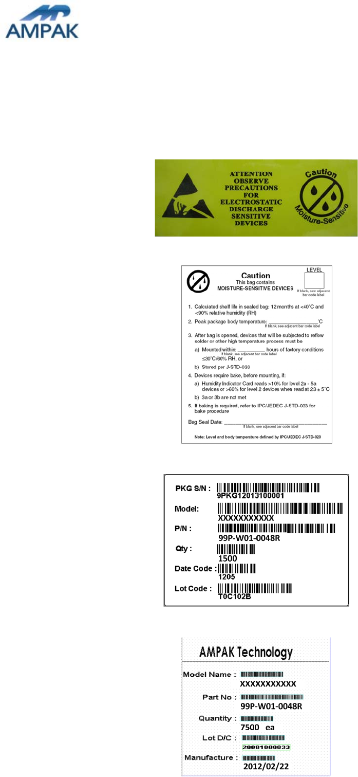
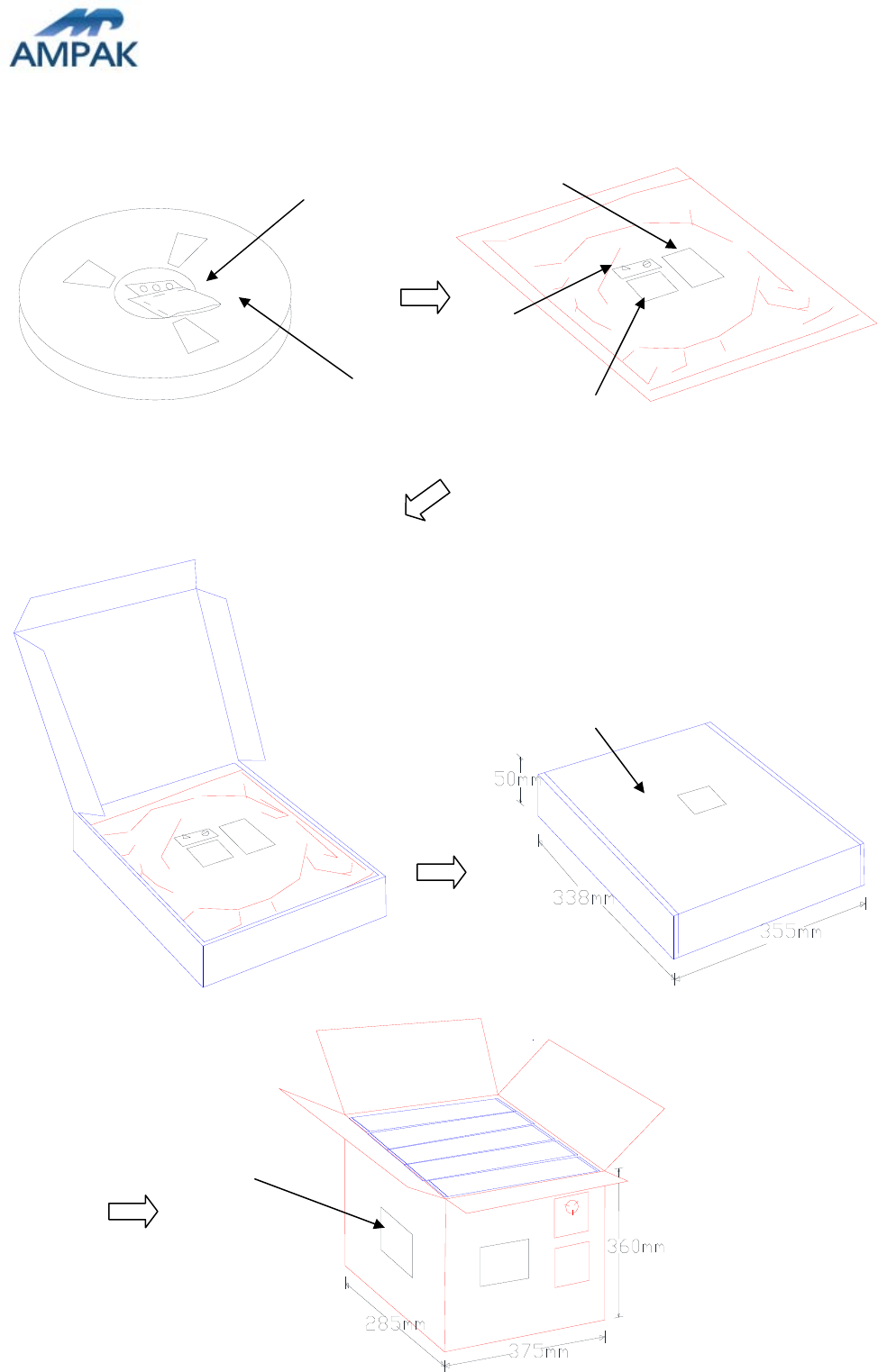
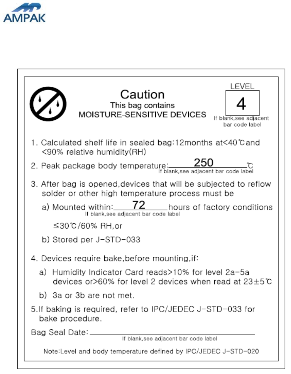
13. Package Information
13.1Label
Label A Anti-static and humidity notice
Label B MSL caution / Storage Condition
Label C Inner box label .
Label D Carton box label .
AMPAK
CONFIDENTIAL
保存期限:最新版本 C-RD-047A
24
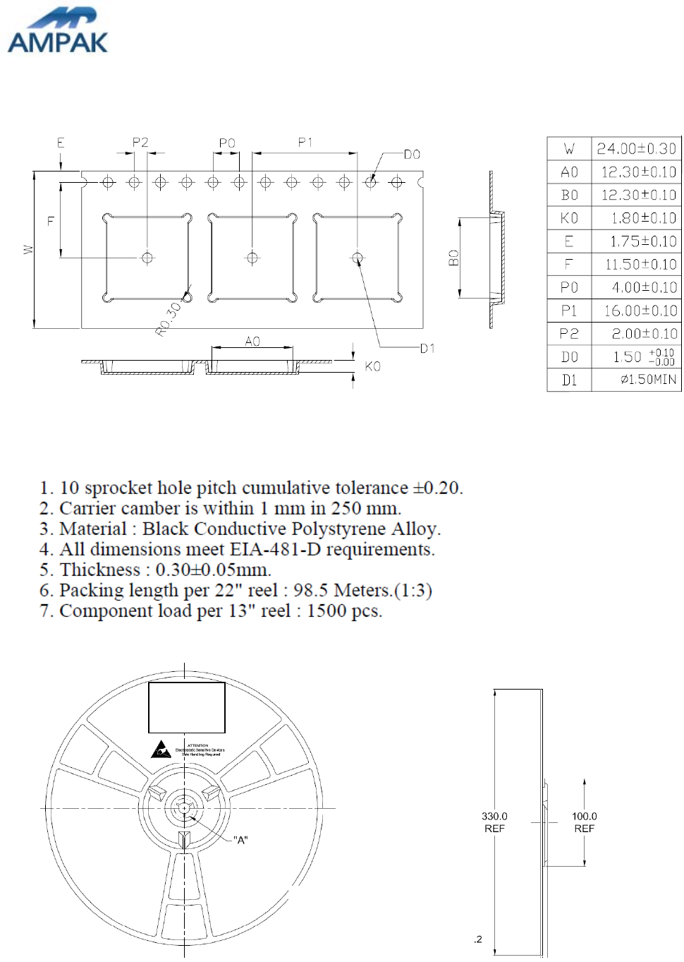
13.2 Dimension
AMPAK
CONFIDENTIAL
保存期限:最新版本 C-RD-047A
25
A
B
C
Humidity indicator
Desiccant
C
D
AMPAK
CONFIDENTIAL
保存期限:最新版本 C-RD-047A
26
13.3 MSL Level / Storage Condition
※NOTE : Accumulated baking time should not exceed 96hrs