Fluke Electronics 805FC Vibration Meter User Manual 2450AT42B100x
Fluke Electronics Vibration Meter 2450AT42B100x
Contents
- 1. User Manual
- 2. RF Exposure Warning Statement
- 3. Antenna Information
Antenna Information

2450 MHz Small SMD Chi
p
Antenna P/N 2450AT42B100
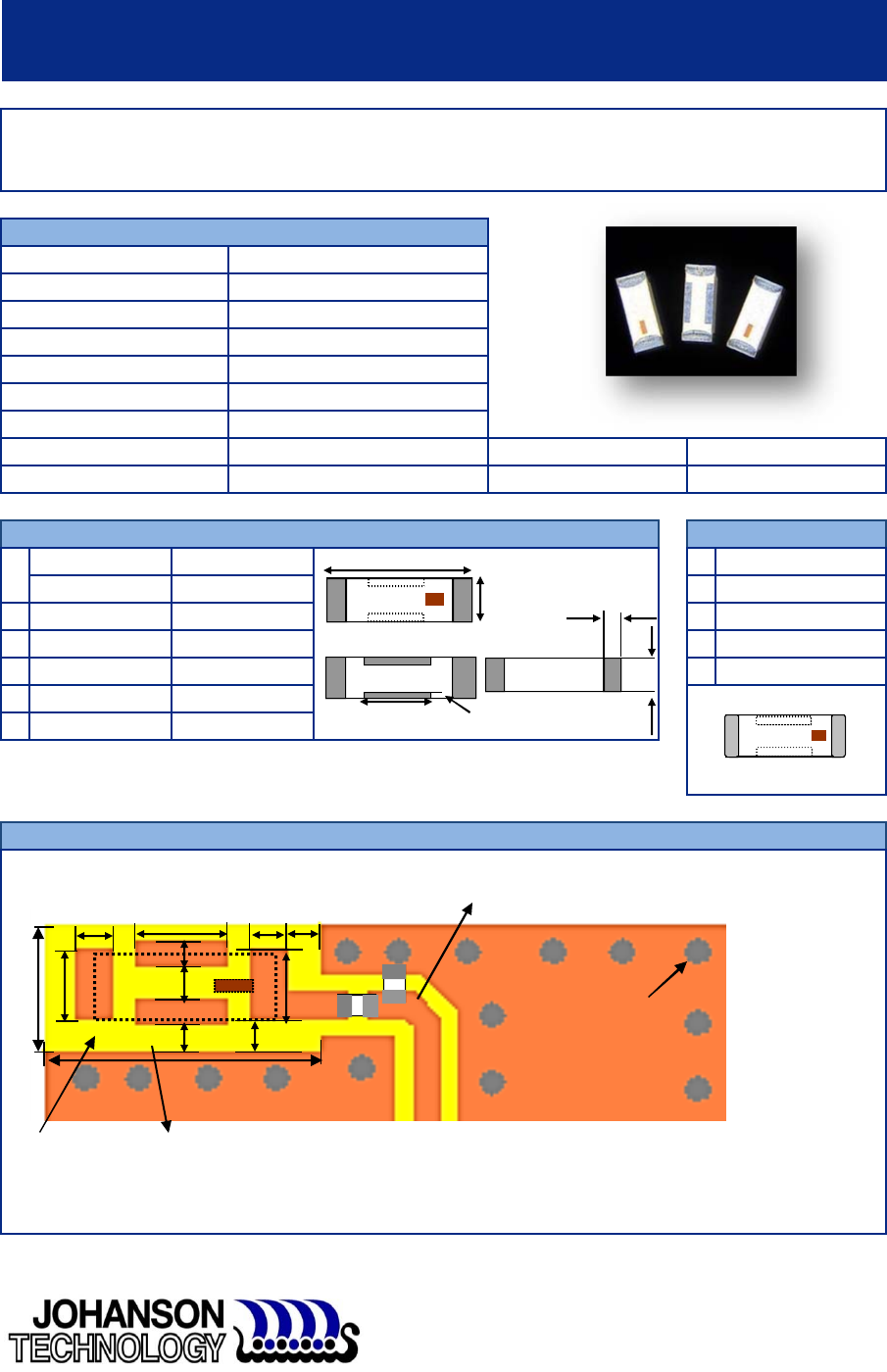
Ground Clearance Requirements Minimized. This antenna was designed for corner or end-mounting
Detail Specification: 10/08/13 Page 1 of 4
In mm
No.
L
±±
1
W
±±
2
L1
±±
3
W1
±±
4
T
a
±±
Johanson Technology, Inc. reserves the right to make design changes without notice.
All sales are subject to Johanson Technology, Inc. terms and conditions.
www.johansontechnology.com
4001 Calle Tecate • Camarillo, CA 93012 • TEL 805.389.1166 FAX 805.389.1821
Ver 2.1
2013 Johanson Technology, Inc. All Rights Reserved
Note: It is recommended that the designer leave available slots for a "pi" (or shunt-series-
shunt) network. The antenna matching network values here are used when antenna is
mounted on Johanson's evaluation board. The matching values on clinet's PCB will be
different, go to: johansontechnology.com/tuning and see how to obtain the new values. If
you need further help, contact our RF Applications Eng Team at:
www.johansontechnology.com/en/ask-a-technical-question.html
We peform layout review
as well as antenna
tuning and
characterization services.
Go to page 2 for details.
General Specifications
-40 to +85°C
2W max. (CW)
2,000
50
9.5 dB min.
-1.5 dBi typ. (XZ-V)
0 dBi typ. (XZ-V)
2400 - 2500 Mhz
0.020 0.012 0.50 0.30
0.079 2.00+.004/-.008 +0.1/-0.2
0.008 0.20
0.50
0.008 0.20
2.60 0.20
+5 ~ +35 °C,Humidity 45~75%RH
-40 to +85°C
"High Frequency Ceramic Solutions"
0.20
2.00
0.020
0.102 0.008
0.008
0.197
0.079
5.00
NC
NC
NC
2450AT42B100
Mounting Considerations
Part Number
Frequency Range
Peak Gain
Average Gain
Return Loss
Impedance
Reel Quanity
Power Capacity
Function
Mechanical Dimensions Terminal Configuration
Feeding Point
Operating Temperature
Recommended Storage Conditio
n
Storage Period
a
T
W1
L1
W
L
2.8 10.711
0.7
1.0
3
0.7
0.8
2
0.7
1
22
8
3.8
6
3.3 nH
1.5 nH
Linewidthshouldbedesignedtomatch50Ωcharacteristicimpedance(GroundedCo‐PlanarWaveguide),dependingonPCBmaterial
andthickness.(Thematchingcircuitandcomponentvalueswillbedifferent onclients PCBlayout, senotesbelowandgotopage2for
details).
Top View
Bottom View
Side View
Yellow
area=Ground/Metal
Clearance.
The "0.82mm" dimmension is
a min. requirement, if the
designer can make this larger,
the better radiation and gain
will occur (i.e. 2.0 or 4.0mm)
RF Via"stich" around
antenna clearance
and feed trace for
best radiation

2450 MHz Small SMD Chi
p
Antenna P/N 2450AT42B100
Detail Specification: 10/08/13 Page 2 of 4
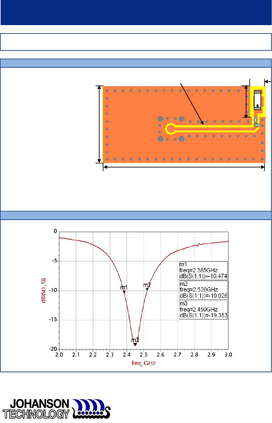
Test Board:
P/N: 2450AT42B100-EB1SMA
(orderable item)
To order, go to:
www.johansontechnology.com/samplerequest
Johanson Technology, Inc. reserves the right to make design changes without notice.
All sales are subject to Johanson Technology, Inc. terms and conditions.
www.johansontechnology.com
4001 Calle Tecate • Camarillo, CA 93012 • TEL 805.389.1166 FAX 805.389.1821
Ver 2.1
2013 Johanson Technology, Inc. All Rights Reserved
Typical Electrical Characteristics (T=25
o
C)
We offer antenna layout review, tuning, and characterization services, go to:
www.johansontechnology.com/ipcantennaservices for details and instructions
Johanson Evaluation Board (orderable item)
"High Frequency Ceramic Solutions"
3.86
40
20
8
(Units in mm)
ReturnLoss
(with
matching)
This 50Feedline can be as short as
needed, this lenth is just for reference to
our EVB

2450 MHz Small SMD Chi
p
Antenna P/N 2450AT42B100
Detail Specification: 10/08/13 Page 3 of 4
Johanson Technology, Inc. reserves the right to make design changes without notice.
All sales are subject to Johanson Technology, Inc. terms and conditions.
www.johansontechnology.com
4001 Calle Tecate • Camarillo, CA 93012 • TEL 805.389.1166 FAX 805.389.1821
Ver 2.1
2013 Johanson Technology, Inc. All Rights Reserved
Typical Electrical Characteristics (T=25
o
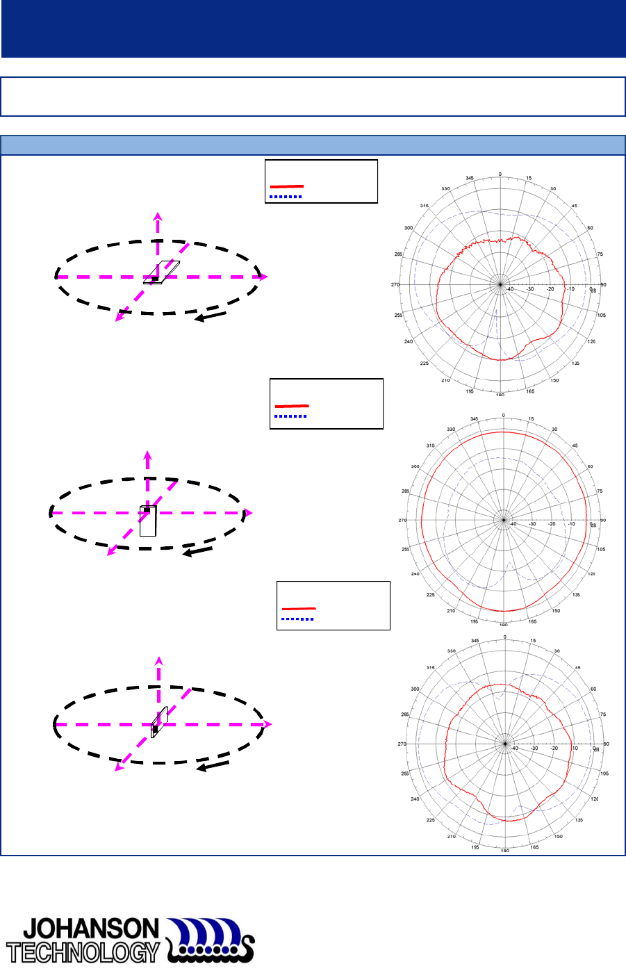
C) Radiation Patterns
"High Frequency Ceramic Solutions"
XY-V/XY-H
180o
270o
0o
90o
X
Z
Y
XY-cut scanning direction
XZ-V/XZ-H
180o
270o
0o
90o
X
Z
Y
XZ-cut scanning direction
YZ-V/YZ-
H
180o
270o
0o
90o
X
Z
Y
YZ-cut scanning direction
XY cut @2.45GHz
Vertical
Horizontal
XZ cut @2.45GHz
Vertical
Horizontal
YZ cut @2.45GHz
Vertical
Horizontal

2450 MHz Small SMD Chi
p
Antenna P/N 2450AT42B100
Detail Specification: 10/08/13 Page 4 of 4
Johanson Technology, Inc. reserves the right to make design changes without notice.
All sales are subject to Johanson Technology, Inc. terms and conditions.
www.johansontechnology.com
4001 Calle Tecate • Camarillo, CA 93012 • TEL 805.389.1166 FAX 805.389.1821
Ver 2.1
2013 Johanson Technology, Inc. All Rights Reserved
www.johansontechnology.com/technical-notes/rohs-compliance.html
RoHS Compliance
MSL Info
www.johansontechnology.com/technical-notes/msl-rating.html
www.johansontechnology.com/ipcantennaservices
"High Frequency Ceramic Solutions"
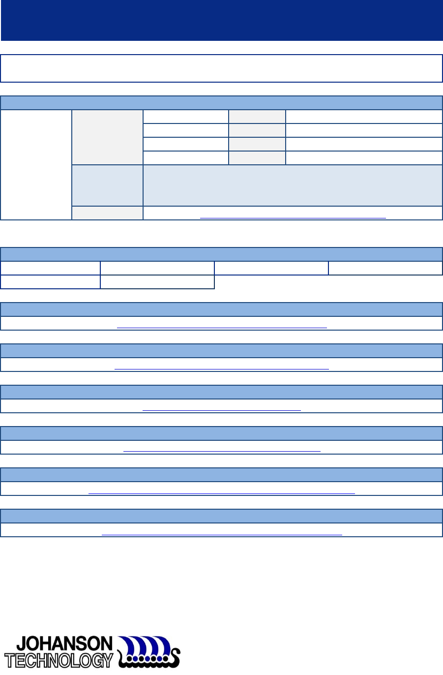
Part Number Explanation
P/N Suffix
Packing Style
Bulk (loose pieces) Suffix = S eg.2450AT42B100S
T & R Suffix = E eg. 2450AT42B100E
Temperature: +5C to +35°C Shelf Life: 18 months max.
T & R (Reverse) Suffix = R eg. 2450AT42B100R (MOQ Applies)
100% Tin Suffix = None eg. 2450AT42B100(S, E, R)
Eval Board (1-port
SMA antenna test
boards)
2450AT42B100-EB1SMA (Page 2)
More Details www.johansontechnology.com/ipc-pn-explained
Storage Conditions and Shelf Life (On T&R or Bulk)
Relative Humidity: 45 to 75%
Packaging information
Soldering Information
Antenna layout and tuning techniques
www.johansontechnology.com/ipcsoldering-profile
www.johansontechnology.com/ipcpackaging.html
Antenna layout review, tuning, and characterization services
www.johansontechnology.com/tuning