Freescale Semiconductor 1231X-MRB Developmental Board User Manual 12311DHRM
Freescale Semiconductor, Inc. Developmental Board 12311DHRM
manual

Document Number: 12311DHRM
Rev. 1
03/2012
12311 Development Hardware
Reference Manual

How to Reach Us:
Home Page:
www.freescale.com
E-mail:
support@freescale.com
USA/Europe or Locations Not Listed:
Freescale Semiconductor
Technical Information Center, CH370
1300 N. Alma School Road
Chandler, Arizona 85224
+1-800-521-6274 or +1-480-768-2130
support@freescale.com
Europe, Middle East, and Africa:
Freescale Halbleiter Deutschland GmbH
Technical Information Center
Schatzbogen 7
81829 Muenchen, Germany
+44 1296 380 456 (English)
+46 8 52200080 (English)
+49 89 92103 559 (German)
+33 1 69 35 48 48 (French)
support@freescale.com
Japan:
Freescale Semiconductor Japan Ltd.
Headquarters
ARCO Tower 15F
1-8-1, Shimo-Meguro, Meguro-ku,
Tokyo 153-0064, Japan
0120 191014 or +81 3 5437 9125
support.japan@freescale.com
Asia/Pacific:
Freescale Semiconductor Hong Kong Ltd.
Technical Information Center
2 Dai King Street
Tai Po Industrial Estate
Tai Po, N.T., Hong Kong
+800 2666 8080
support.asia@freescale.com
For Literature Requests Only:
Freescale Semiconductor Literature Distribution Center
P.O. Box 5405
Denver, Colorado 80217
1-800-521-6274 or 303-675-2140
Fax: 303-675-2150
LDCForFreescaleSemiconductor@hibbertgroup.com
Information in this document is provided solely to enable system and software implementers to use
Freescale Semiconductor products. There are no express or implied copyright licenses granted
hereunder to design or fabricate any integrated circuits or integrated circuits based on the information
in this document.
Freescale Semiconductor reserves the right to make changes without further notice to any products
herein. Freescale Semiconductor makes no warranty, representation or guarantee regarding the
suitability of its products for any particular purpose, nor does Freescale Semiconductor assume any
liability arising out of the application or use of any product or circuit, and specifically disclaims any
and all liability, including without limitation consequential or incidental damages. “Typical” parameters
that may be provided in Freescale Semiconductor data sheets and/or specifications can and do vary
in different applications and actual performance may vary over time. All operating parameters,
including “Typicals”, must be validated for each customer application by customer’s technical
experts. Freescale Semiconductor does not convey any license under its patent rights nor the rights
of others. Freescale Semiconductor products are not designed, intended, or authorized for use as
components in systems intended for surgical implant into the body, or other applications intended to
support or sustain life, or for any other application in which the failure of the Freescale Semiconductor
product could create a situation where personal injury or death may occur. Should Buyer purchase
or use Freescale Semiconductor products for any such unintended or unauthorized application,
Buyer shall indemnify and hold Freescale Semiconductor and its officers, employees, subsidiaries,
affiliates, and distributors harmless against all claims, costs, damages, and expenses, and
reasonable attorney fees arising out of, directly or indirectly, any claim of personal injury or death
associated with such unintended or unauthorized use, even if such claim alleges that Freescale
Semiconductor was negligent regarding the design or manufacture of the part.
Freescale™ and the Freescale logo are trademarks of Freescale Semiconductor, Inc. All other
product or service names are the property of their respective owners.
© Freescale Semiconductor, Inc. 2007, 2008, 2009, 2010, 2011, 2012. All rights reserved.

12311 Development Hardware Reference Manual, Rev. 1
Freescale Semiconductor iii
Contents
About This Book
Audience . . . . . . . . . . . . . . . . . . . . . . . . . . . . . . . . . . . . . . . . . . . . . . . . . . . . . . . . . . . . . . . . . . . . . v
Organization . . . . . . . . . . . . . . . . . . . . . . . . . . . . . . . . . . . . . . . . . . . . . . . . . . . . . . . . . . . . . . . . . . v
Revision History . . . . . . . . . . . . . . . . . . . . . . . . . . . . . . . . . . . . . . . . . . . . . . . . . . . . . . . . . . . . . . . v
Chapter 1
Safety Information
1.1 FCC Guidelines. . . . . . . . . . . . . . . . . . . . . . . . . . . . . . . . . . . . . . . . . . . . . . . . . . . . . . . . . . . . . . 1-1
1.1.1 Labeling . . . . . . . . . . . . . . . . . . . . . . . . . . . . . . . . . . . . . . . . . . . . . . . . . . . . . . . . . . . . . . . . 1-1
1.1.2 Operating Conditions . . . . . . . . . . . . . . . . . . . . . . . . . . . . . . . . . . . . . . . . . . . . . . . . . . . . . . 1-1
1.1.3 Exposure Limits . . . . . . . . . . . . . . . . . . . . . . . . . . . . . . . . . . . . . . . . . . . . . . . . . . . . . . . . . . 1-1
1.1.4 Antenna Restrictions. . . . . . . . . . . . . . . . . . . . . . . . . . . . . . . . . . . . . . . . . . . . . . . . . . . . . . . 1-1
1.2 Regulatory Approval For Canada (IC RSS 210) . . . . . . . . . . . . . . . . . . . . . . . . . . . . . . . . . . . . 1-2
1.2.1 26 PART 5 – Appendix . . . . . . . . . . . . . . . . . . . . . . . . . . . . . . . . . . . . . . . . . . . . . . . . . . . . 1-2
1.3 Electrostatic Discharge Considerations . . . . . . . . . . . . . . . . . . . . . . . . . . . . . . . . . . . . . . . . . . . 1-2
1.4 Disposal Instructions. . . . . . . . . . . . . . . . . . . . . . . . . . . . . . . . . . . . . . . . . . . . . . . . . . . . . . . . . . 1-2
Chapter 2
MC12311 Development Platform Overview and Description
2.1 Introduction. . . . . . . . . . . . . . . . . . . . . . . . . . . . . . . . . . . . . . . . . . . . . . . . . . . . . . . . . . . . . . . . . 2-1
2.2 Features. . . . . . . . . . . . . . . . . . . . . . . . . . . . . . . . . . . . . . . . . . . . . . . . . . . . . . . . . . . . . . . . . . . . 2-2
2.2.1 TWR-RF Module . . . . . . . . . . . . . . . . . . . . . . . . . . . . . . . . . . . . . . . . . . . . . . . . . . . . . . . . . 2-3
2.3 Driver Considerations . . . . . . . . . . . . . . . . . . . . . . . . . . . . . . . . . . . . . . . . . . . . . . . . . . . . . . . . . 2-4
Chapter 3
12311-MRB
3.1 12311-MRB Overview . . . . . . . . . . . . . . . . . . . . . . . . . . . . . . . . . . . . . . . . . . . . . . . . . . . . . . . . 3-1
3.1.1 Features. . . . . . . . . . . . . . . . . . . . . . . . . . . . . . . . . . . . . . . . . . . . . . . . . . . . . . . . . . . . . . . . . 3-1
3.1.2 Form Factor. . . . . . . . . . . . . . . . . . . . . . . . . . . . . . . . . . . . . . . . . . . . . . . . . . . . . . . . . . . . . . 3-2
3.1.3 Board Level Specifications. . . . . . . . . . . . . . . . . . . . . . . . . . . . . . . . . . . . . . . . . . . . . . . . . . 3-3
3.2 Functional Description . . . . . . . . . . . . . . . . . . . . . . . . . . . . . . . . . . . . . . . . . . . . . . . . . . . . . . . . 3-5
3.2.1 RF Performance and Considerations . . . . . . . . . . . . . . . . . . . . . . . . . . . . . . . . . . . . . . . . . . 3-5
3.2.2 Clocks . . . . . . . . . . . . . . . . . . . . . . . . . . . . . . . . . . . . . . . . . . . . . . . . . . . . . . . . . . . . . . . . . . 3-6
3.3 Reset and BDM Debug Port . . . . . . . . . . . . . . . . . . . . . . . . . . . . . . . . . . . . . . . . . . . . . . . . . . . . 3-8
3.3.1 Power Management . . . . . . . . . . . . . . . . . . . . . . . . . . . . . . . . . . . . . . . . . . . . . . . . . . . . . . . 3-9
3.3.2 IO Connectors J2 and J3 . . . . . . . . . . . . . . . . . . . . . . . . . . . . . . . . . . . . . . . . . . . . . . . . . . . 3-11
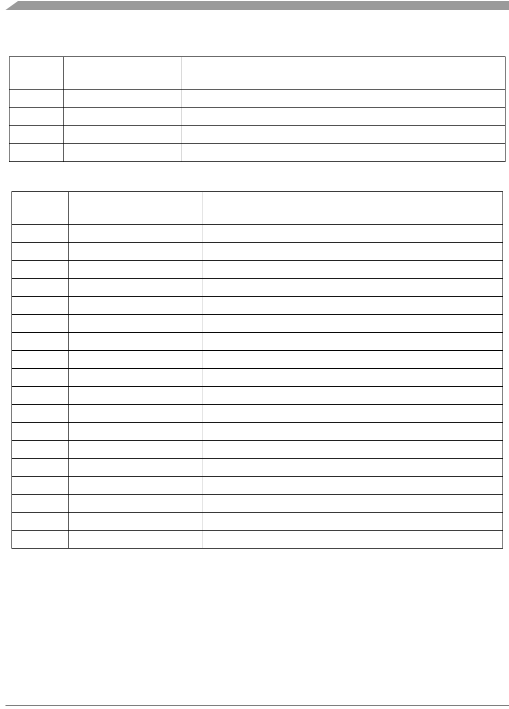
3.4 Schematic, Board Layout, and Bill of Material . . . . . . . . . . . . . . . . . . . . . . . . . . . . . . . . . . . . 3-13
3.4.1 Bill of Materials . . . . . . . . . . . . . . . . . . . . . . . . . . . . . . . . . . . . . . . . . . . . . . . . . . . . . . . . . 3-16

12311 Development Hardware Reference Manual, Rev. 1
iv Freescale Semiconductor
Chapter 4
PCB Manufacturing Specifications
4.1 Single PCB Construction . . . . . . . . . . . . . . . . . . . . . . . . . . . . . . . . . . . . . . . . . . . . . . . . . . . . . . 4-1
4.2 Panelization. . . . . . . . . . . . . . . . . . . . . . . . . . . . . . . . . . . . . . . . . . . . . . . . . . . . . . . . . . . . . . . . . 4-2
4.3 Materials . . . . . . . . . . . . . . . . . . . . . . . . . . . . . . . . . . . . . . . . . . . . . . . . . . . . . . . . . . . . . . . . . . . 4-2
4.4 Solder Mask . . . . . . . . . . . . . . . . . . . . . . . . . . . . . . . . . . . . . . . . . . . . . . . . . . . . . . . . . . . . . . . . 4-3
4.5 Silk Screen . . . . . . . . . . . . . . . . . . . . . . . . . . . . . . . . . . . . . . . . . . . . . . . . . . . . . . . . . . . . . . . . . 4-3
4.6 Electrical PCB Testing . . . . . . . . . . . . . . . . . . . . . . . . . . . . . . . . . . . . . . . . . . . . . . . . . . . . . . . . 4-3
4.7 Packaging . . . . . . . . . . . . . . . . . . . . . . . . . . . . . . . . . . . . . . . . . . . . . . . . . . . . . . . . . . . . . . . . . . 4-3
4.8 Hole Specification/Tool Table . . . . . . . . . . . . . . . . . . . . . . . . . . . . . . . . . . . . . . . . . . . . . . . . . . 4-3
4.9 File Description. . . . . . . . . . . . . . . . . . . . . . . . . . . . . . . . . . . . . . . . . . . . . . . . . . . . . . . . . . . . . . 4-4

12311 Development Hardware Reference Manual, Rev. 1
Freescale Semiconductor v
About This Book
This manual describes Freescale’s 12311-MRB development platform hardware. The MC12311
development platform is a highly-integrated, cost-effective, system-in-package (SIP), sub-1GHz wireless
node solution with an FSK or OOK modulation-capable transceiver and low-power QE32 8-bit
microcontroller.
Audience
This manual is intended for system designers.
Organization
This document is organized into the following chapters.
Chapter 1 Safety Information — Highlights some of the FCC requirements.
Chapter 2 HCS08 Development Platform Overview and Description — Provides an
overview of the two boards that comprise the MC12311 development platform.
Chapter 3 Modular Reference Board — This chapter details the 12311-MRB evaluation
board based on the Freescale MC12311 device.
Chapter 4 PCB Manufacturing Specifications — This chapter provides the specifications
used to manufacture the various 12311-MRB printed circuit boards (PCBs).
Revision History
The following table summarizes revisions to this document since the previous release (Rev 0.0).
Revision History
Location Revision
Chapter 3 New schematic for Figure 3-9.

12311 Development Hardware Reference Manual, Rev. 1
vi Freescale Semiconductor
Definitions, Acronyms, and Abbreviations
The following list defines the acronyms and abbreviations used in this document.
ADC Analog to Digital Converter
AES Advanced Encryption Standard
CTS Clear to Send
DAC Digital to Analog Converter
I2C Inter-Integrated Circuit is a multi-master serial computer bus
ISM Industrial Scientific Medical 2.4 GHz radio frequency band
JTAG Joint Test Action Group
LGA Land Grid Array
MAC Media Access Controller
MCU Microcontroller Unit
PCB Printed circuit board
PiP Platform in Package
PWM Pulse-width modulation
RCM Remote Control Module
REM Remote Extender Board
RTS Request to Send
SMA Connector SubMiniature version “A” connector
SPI Serial Peripheral Interface
SSI Synchronous Serial Interface
TACT Switch A switch that provides a slight “snap” or “click” to the user to indicate function.
TELCO Telephone Company
USB Universal Serial Bus
VCP Virtual Com Port

12311 Development Hardware Reference Manual, Rev. 1
Freescale Semiconductor 1-1
Chapter 1
Safety Information
1.1 FCC Guidelines
This equipment is for use by developers for evaluation purposes only and must not be incorporated into
any other device or system. This device may not be sold to the general public. Integrators will be
responsible for reevaluating the end product (including the transmitter) and obtaining a separate FCC
authorization.
FCC approval of this device only covers the original configuration of this device as supplied. Any
modifications to this product, including changes shown in this manual, may violate the rules of the Federal
Communications Commission and Industry Canada and make operation of the product unlawful.
1.1.1 Labeling
FCC labels are physically located on the back of the board.
1.1.2 Operating Conditions
This device complies with part 15 of the FCC Rules. Operation is subject to the following two conditions:
• This device may not cause harmful interference.
• This device must accept any interference received, including interference that may cause undesired
operation.
1.1.3 Exposure Limits
This equipment complies with FCC radiation exposure limits set forth for an uncontrolled environment.
The antenna(s) used for this equipment must be installed to provide a separation distance of at least 8
inches (20cm) from all persons.
1.1.4 Antenna Restrictions
An intentional radiator shall be designed to ensure that no antenna other than that furnished by the
responsible party shall be used with the device. The use of a permanently attached antenna or of an
antenna that uses a unique coupling to the intentional radiator shall be considered sufficient to comply with
the provisions of this Section. The manufacturer may design the unit so that a broken antenna can be
replaced by the user, but the use of a standard antenna jack or electrical connector is prohibited. This
requirement does not apply to carrier current devices or to devices operated under the provisions of
Sections 15.211, 15.213, 15.217, 15.219, or 15.221. Further, this requirement does not apply to intentional

Safety Information
12311 Development Hardware Reference Manual, Rev. 1
1-2 Freescale Semiconductor
radiators that must be professionally installed, such as perimeter protection systems and some field
disturbance sensors, or to other intentional radiators which, in accordance with Section 15.31(d), must be
measured at the installation site. However, the installer shall be responsible for ensuring that the proper
antenna is employed so that the limits in this Part are not exceeded.
1.2 Regulatory Approval For Canada (IC RSS 210)
This device complies with Industry Canada licence-exempt RSS standard(s). Operation is subject to the
following two conditions:
1. This device may not cause interference, and
2. This device must accept any interference, including interference that may cause undesired
operation of the device.
1.2.1 26 PART 5 – Appendix
Le présent appareil est conforme aux CNR d'Industrie Canada applicables aux appareils radio exempts de
licence. L'exploitation est autorisée aux deux conditions suivantes:
1. l'appareil ne doit pas produire de brouillage, et
2. l'utilisateur de l'appareil doit accepter tout brouillage radioélectrique subi, même si le brouillage
est susceptible d'en compromettre le fonctionnement.
1.3 Electrostatic Discharge Considerations
Although damage from electrostatic discharge (ESD) is much less common on these devices than on early
CMOS circuits, normal handling precautions should be used to avoid exposure to static discharge.
Qualification tests are performed to ensure that these devices can withstand exposure to reasonable levels
of static without suffering any permanent damage.
All ESD testing is in conformity with the JESD22 Stress Test Qualification for Commercial Grade
Integrated Circuits. During the device qualification ESD stresses were performed for the human body
model (HBM), the machine model (MM) and the charge device model (CDM).
All latch-up test testing is in conformity with the JESD78 IC Latch-Up Test.
When operating or handling the development boards or components, Freescale strongly recommends
using at least the grounding wrist straps plus any or all of the following ESD dissipation methods:
• Flexible fabric, solid fixed size, or disposable ESD wrist straps
• Static control workstations, static control monitors and table or floor static control systems
• Static control packaging and transportation materials and environmental systems
1.4 Disposal Instructions
This product may be subject to special disposal requirements. For product disposal instructions, refer to
www.freescale.com/productdisposal.

12311 Development Hardware Reference Manual, Rev. 1
Freescale Semiconductor 2-1
Chapter 2
MC12311 Development Platform Overview and Description
2.1 Introduction
The MC12311 development platform is an evaluation environment based on the Freescale MC12311
device. The MC12311 is a highly-integrated, cost-effective, system-in-package (SIP), sub-1GHz wireless
node solution with an FSK or OOK modulation-capable transceiver and low-power QE32 8-bit
microcontroller. This configuration allows users to minimize the use of external components.
The MC12311 is targeted for the following low-power wireless applications:
• Automated Meter Reading
• Wireless Sensor Networks
• Home and Building Automation
• Wireless Alarm and Security Systems
• Industrial Monitoring and Control
• Wireless MBUS Standard (EN13757-4:2005)
Freescale supplements the MC12311 with tools and software that include hardware evaluation and
development boards, software development IDE and applications, drivers, custom PHY usable with
Freescale’s IEEE 802.15.4 compatible MAC, and an available wireless MBUS solution.
The MC12311 development platform is comprised of two boards:
• 12311-Modular Reference Board (12311-MRB) - this board contains the MC12311 device with 32
MHz reference oscillator crystal, RF circuitry including antenna, and supporting circuitry. The
board can be used as a simple standalone evaluation platform or as a daughter card to the other
MC12311 development platform boards or to a custom, application specific motherboard.
— Provides compact reference design for device footprint and RF layout
— Provides pre-designed MC12311 hardware (device and function)
— Provides access to the MC12311 full set of GPIO
— Provides MCU BDM debug port
— Provides optional local 2 Mbit serial FLASH, 32.768 kHz oscillator crystal, IR “blaster” LED
and power management.
• TWR-RF Board . The TWR-RF board is a motherboard for the MC12311 and 12311-MRB
daughter boards, to enable its use within the Tower system. The TWR-RF board is a Tower
Controller Module compatible with the Freescale Tower System. The 12311-MRB + TWR-RF can
run standalone, outside the Tower system. The following list summarizes the features of the
TWR-RF Module:
MC12311 Development Platform Overview and Description
12311 Development Hardware Reference Manual, Rev. 1
2-2 Freescale Semiconductor
— Standard sockets 100 mils J5 and J4 (2X9 and 2x10) to connect MC12311 and 12311-MRB
daughter boards
— Standard header 100 mils J1 (2x20) to enable signalling path to TWR primary and secondary
connectors.
— Standard header 100 mils J6 (3x12) to enable signalling to on board HW and USB interface or
to TWR system Hardware
— On-board regulator to provide external supply
— Four (4) user-controllable LEDs
— Four (4) user push-button switches
— USB Type B connector
Whether the 12311-MRB is used in a simple standalone application or in combination with another host
card, Freescale provides a complete software development environment called the Freescale BeeKit
Wireless Connectivity Toolkit (BeeKit). BeeKit is a comprehensive codebase of wireless networking
libraries, application templates, and sample applications. The BeeKit Graphical User Interface (GUI)
allows users to create, modify, and update various wireless networking implementations. A wide range of
software functionality is available to complement the 12311-MRB and these are provided as codebases
within BeeKit.
2.2 Features
The MC12311 development platform is built around the concept of having a single daughter card
(12311-MRB) that contains the MC12311 IC and all necessary I/O connections for use as a self-contained
module or for connection to an application motherboard like the TWR-RF board.
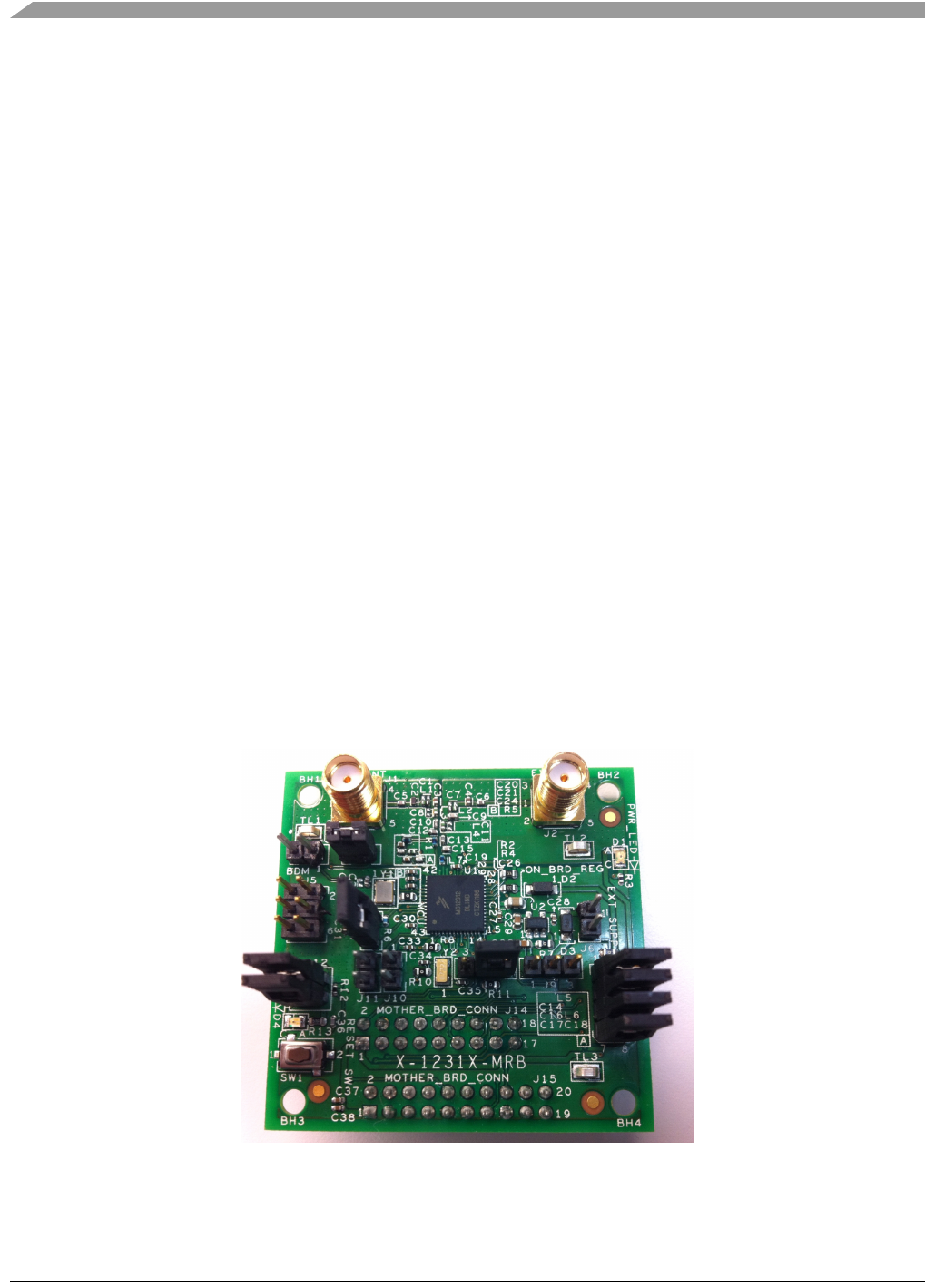
Figure 2-1 shows a photo of the 12311-MRB.
Figure 2-1. 12311-MRB
Features of the MC12311 development platform include:

MC12311 Development Platform Overview and Description
12311 Development Hardware Reference Manual, Rev. 1
Freescale Semiconductor 2-3
• Based on Freescale’s low-cost MC12311 sub-1GHz wireless node solution with an FSK or OOK
modulation-capable transceiver and low-power QE32 8-bit microcontroller, and a functional set of
MCU peripherals into a 60-pin LGA package
• Reference design area with small footprint, low cost RF node
— Unbalance input/output port
— Flexible RF-Front End for different bands operation
— High Sensitivity: down to -120dBm at 1.2kbps
• 32 MHz reference oscillator
• BDM serial MCU debug port
• Optional secondary 32.768 kHz crystal oscillator for accurate low power timing
• Master reset switch
• Full power regulation and management
• 12311-MRB board provides
— Required circuitry for MC12311 - crystals and RF circuitry
— Local power supply regulation
— Access to all GPIO
— Standalone or daughter card use modes
— BDM connector
2.2.1 TWR-RF Module
The 12311-MRB can run in the Freescale Tower System using the RF-Tower module (TWR-RF). Features
of the TWR-RF module include:
• Standard sockets 100 mils J5 and J4 (2 x 9 and 2 x 10) to connect either a 1323x Modular Reference
Board (1323x-MRB) or a 12311 Modular Reference Board (12311-MRB)
• Standard header 100 mils J1 (2 x 20) to enable signalling path to TWR primary and secondary
connectors.
• Standard header 100 mils J6 (3 x 12) to enable signalling to on board HW and USB interface or to
TWR system Hardware
• On-board regulator to provide external supply
• Four (4) user-controllable LEDs
• Four (4) user push-button switches
• USB Type B connector
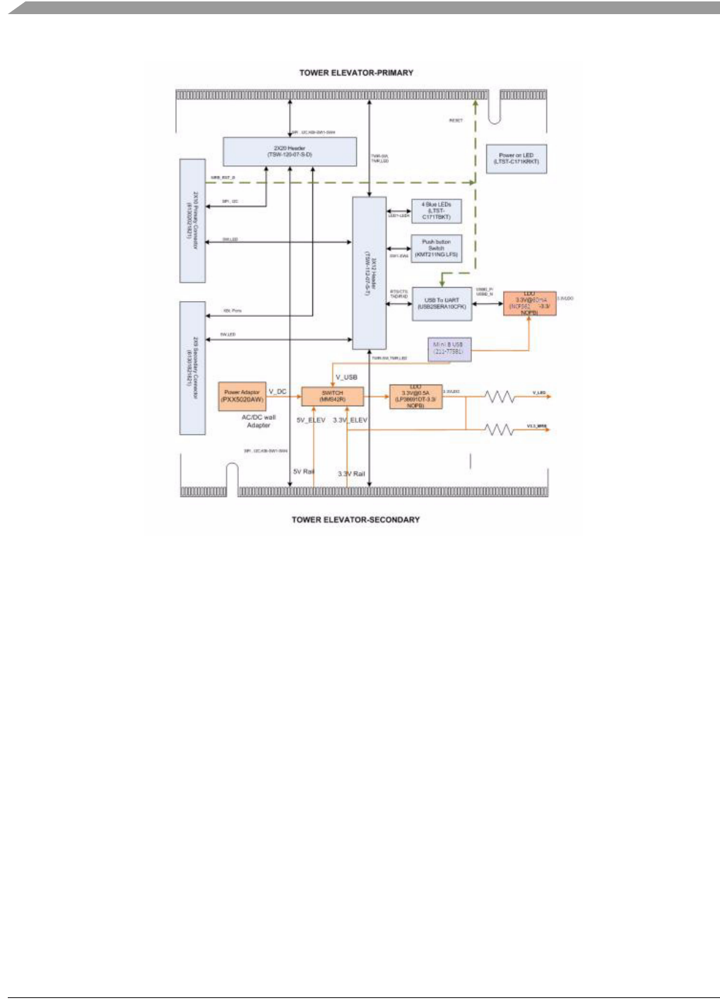
Figure 2-2 shows a simplified block diagram of the Freescale Tower RF system.
MC12311 Development Platform Overview and Description
12311 Development Hardware Reference Manual, Rev. 1
2-4 Freescale Semiconductor
Figure 2-2. Simplified TWR-RF Block Diagram
See the TWR-RF Reference Manual for more information about the RF-Tower module.
2.3 Driver Considerations
When users first connect a 12311-MRB to a PC, they may be prompted to install drivers. If BeeKit is
installed and this occurs, do not allow Windows to automatically search for and install the drivers. Instead,
select manual installation and steer Windows to the following directory:
C:\Program Files\Freescale\Drivers
If installing the BeeKit software package to another drive or directory, indicate the Drivers directory
created by the installer in the custom location where BeeKit was installed.
Follow the instructions as they appear on the screen to complete driver installation.
If BeeKit is not installed, be aware of the following:
• The boards use FSL USB2SER USB to UART bridge converter.
• Download the appropriate driver and follow the instructions to complete driver installation from
www.freescale.com.

12311 Development Hardware Reference Manual, Rev. 1
Freescale Semiconductor 3-1
Chapter 3
12311-MRB
3.1 12311-MRB Overview
The 12311-MRB is an evaluation board based on the Freescale MC12311 device. The 12311-MRB
provides a platform to evaluate the MC12311 device, develop software and applications. The core device
is accompanied by the 32 MHz reference oscillator crystal, RF circuitry including SMA for antenna
connection and/or instrumentation, and supporting circuitry.
This basic board is intended as the core module for MC12311 evaluation and application development and
can be used in the following modes:
• Simple standalone evaluation platform
• Daughtercard to other Development Platform boards (TWR-RF, 1323x-RCM or 1323x-REM)
• Daughtercard to an application specific motherboard.
3.1.1 Features
The 12311-MRB provides the following features:
• Small form factor (2 x 2 inches)
• 4-Layer metal, 0.034 inch thick FR4 board
• MC12311 reference design area
— LGA footprint and power supply bypass
— 32 MHz reference oscillator crystal
— RF components and layout
• Low cost RF node
— Differential input/output port (typically used with a balun)
— High sensitivity of -120 dBm at 1.2 KBPS
— SMA output connector for Transmit/Receive Output
• Two connectors provided daughter card mounting
— 20-Pin primary connector
— 18-Pin secondary connector
— Provide main supply voltage to board
— Provide access to all MC12311 GPIO
• Flexible board power supply
— 3.3 V LDO series regulator supplied
12311-MRB
12311 Development Hardware Reference Manual, Rev. 1
3-2 Freescale Semiconductor
— Regulator bypass jumper option
— Separate external voltage source option
— Power-on green LED
— Jumpers allow various block current measurements
• 6-Pin BDM serial MCU debug port
• MC12311 reset switch
3.1.2 Form Factor
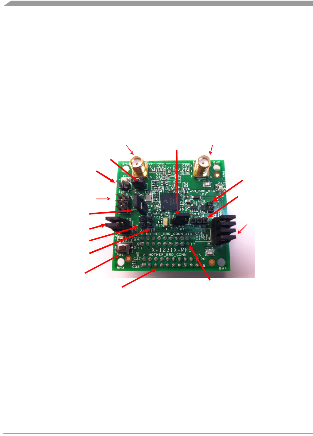
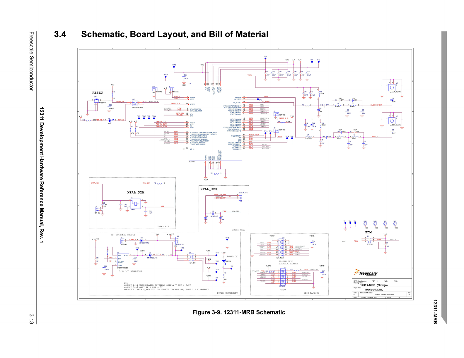
Figure 3-1 shows the 12311-MRB connector and header locations.
Figure 3-1. 12311-MRB
Figure 3-2 shows a footprint of the 12311-MRB with the location of the IO Headers J2 and J3. Users can
create a motherboard to mount the 12311-MRB and headers J2 and J3 are used for that connection.
• Both headers have standard 0.10in / 2.54 mm pin spacing
• J2 is 20-pin and J3 is 18-pin
• Both are pin headers mounted on the bottom side of the 12311-MRB and are intended to plug into
matching receptacles on the motherboard.
BDMport
(J5)
Primary 20‐pinIO
Connector (J15)
Secondary 18‐pinIO
Connector (J14)
RFIOScMA
(J2)
PABoost SMA
(J1)
J13
J6
J9
J8
J3
J4
J12
J11
J7
J10
Reset SW
12311-MRB
12311 Development Hardware Reference Manual, Rev. 1
Freescale Semiconductor 3-3
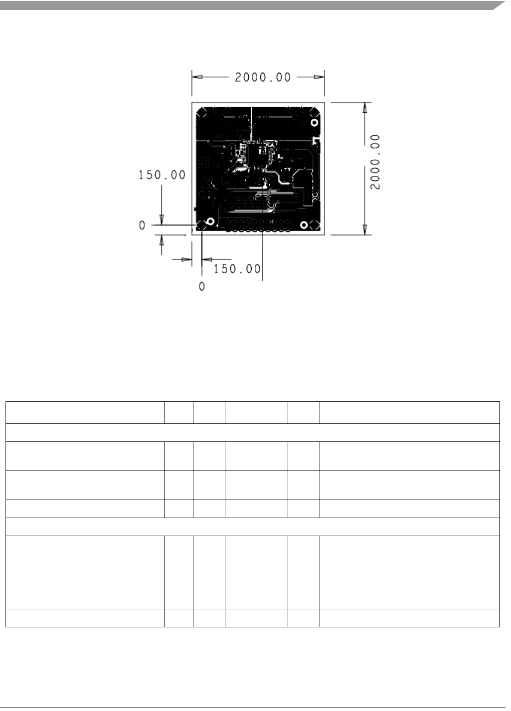
Figure 3-2. 12311-MRB Top Side (Component Side) Footprint
3.1.3 Board Level Specifications
Table 3-1. 12311-MRB Specifications
Parameter Min Typ Max Units Notes/Conditions
General
Size (PCB: X, Y) 51 x 51
2.01 x 2.01
mm
inches
Layer build (PCB) 0.8
0.034
mm
inches
4-Layer
Dielectric material (PCB) FR4
Power
Voltage supply (DC)
With 3.3 V regulator in use 3.50 10 V Full module use
Current consumption TBD mA
12311-MRB
12311 Development Hardware Reference Manual, Rev. 1
3-4 Freescale Semiconductor
Temperature
Operating temperature (see note) -40 +25 +70 °C • Operating temperature is limited to +70
°C due to switches. Basic circuit is good
for a maximum temperature of +85 °C.
Storage temperature -30 +25 +70 °C
RF Receiver
FSK Sensitivity -105
to
-120
dBm
OOK Sensitivity -112 dBm
Adjacent channel Rejection (Offset =
+/- 25 KHz or 50 KHz)
-42 dB
2nd order Intercept point +75 dBm
3rd order Intercept point +20 dBm
RSSI dynamic range -115 0
RF Transmitter
RF Power Output (RFIO pin) -18 -3 dBm Programmable in 1dB steps
Adjacent channel Power (25KHz
offset)
-37 dBm
Regulatory Approval
FCC Product is approved accordingly to the FCC
part 15 standard
CE (ETSI) Product is approved accordingly to the EN
300 328 V1.7.1 (2006-10) standard
CE (EMC) Product is approved accordingly to the EN
301 489-1 V1.6.1 (2005-09) and EN 301
489-17 V1.2.1 (2002-08) standards
Safety
UL Product is approved accordingly to the IEC
60950-1 and EN 60950-1, First Edition
standards
Environment
RoHS Product complies with the EU Directive
2002/95/EC of 27 January 2003
WEEE Product complies with the EU Directive
2002/95/EC of 27 January 2003
Table 3-1. 12311-MRB Specifications (continued)
Parameter Min Typ Max Units Notes/Conditions
12311-MRB
12311 Development Hardware Reference Manual, Rev. 1
Freescale Semiconductor 3-5
3.2 Functional Description
The 12311-MRB is built around Freescale’s MC12311 56-pin LGA platform. Figure 3-2 shows a simple
block diagram. This board is intended as a simple evaluation platform and as a building block for
application development. The 4-layer board provides the MC12311 with its required RF circuitry, 32 MHz
reference oscillator crystal, and power supply bypassing. The layout for this base level functionality can
be used as a reference layout by the user target board.
In additional to the base MC12311 functionality, the 12311-MRB provides features to assist in debug, reset
button, simple power manager, and expansion connectors for the GPIO. In the following sections, refer to:
•Figure 3-1 for location of connectors and features
•Figure 3-3 for the functional blocks
•Figure 3-9 for the board schematic
Figure 3-3. 12311-MRB Block Diagram
3.2.1 RF Performance and Considerations
The MC12311 transceiver is a single-chip integrated circuit ideally suited for today's high performance
ISM band RF applications. It is intended for use as a high-performance, low-cost FSK and OOK RF
transceiver for robust, frequency agile, half-duplex bi-directional RF links. The MC12311 is intended for
applications over a wide frequency range, including the 868 MHz European and the 902-928 MHz North
American ISM bands.
12311-MRB
12311 Development Hardware Reference Manual, Rev. 1
3-6 Freescale Semiconductor
The 12311-MRB uses a flexible RF path topology that make it suitable for working in different frequency
bands by replacing a minimum number of components while providing good RF performance. The
following table shows the different BOM according to different Frequency Bands of operation.
NOTE
See the MC12311 Data Sheet and Reference Manual for more RF design
information.
Figure 3-4. 12311-MRB RF Circuitry
3.2.2 Clocks
The MC12311 provides for two clocks:
• 32 MHz Reference Oscillator - Figure 3-5 shows the external 32 MHz external crystal Y1. This
mounted crystal must meet the MC12311 specifications.
— Capacitors C22 and C25 provide the bulk of the crystal load capacitance.
— Signal DIO5/CLKOUT can be used to supply an external clock to MCU die and to measure a
the 32MHz oscillator frequency.
— The 12311-MRB has provision for injecting an external 32 MHz clock source as an alternative
to use of the onboard crystal:
– The crystal Y1 should be removed
– C23 must be mounted
– The external 32 MHz source is connected to 2-pin header J4.
• Optional 32.768 kHz Crystal Oscillator - Provision is also made for a secondary 32.768 kHz crystal
Y2 (see Figure 3-6). This oscillator can be used for a low power accurate time base.
12311-MRB
12311 Development Hardware Reference Manual, Rev. 1
Freescale Semiconductor 3-7
— The module comes provided with this Y2 crystal and its load capacitors C34 and C35.
— Load capacitors C34 and C35 provide the entire crystal load capacitance
— The 32 kHz oscillator components are supplied, but un-enabled. Zero-ohm resistors R10 and
R11 enable use of IO signals PTB7 and PTB6 via the IO connector
— Use J8 to enable crystal signaling to MCU die from the DIO5 or from the 32kHz crystal.
Figure 3-5. 12311-MRB 32 MHz Reference Oscillator Circuit
Figure 3-6. 12311-MRB 32.768 kHz Optional Oscillator Circuit
12311-MRB
12311 Development Hardware Reference Manual, Rev. 1
3-8 Freescale Semiconductor
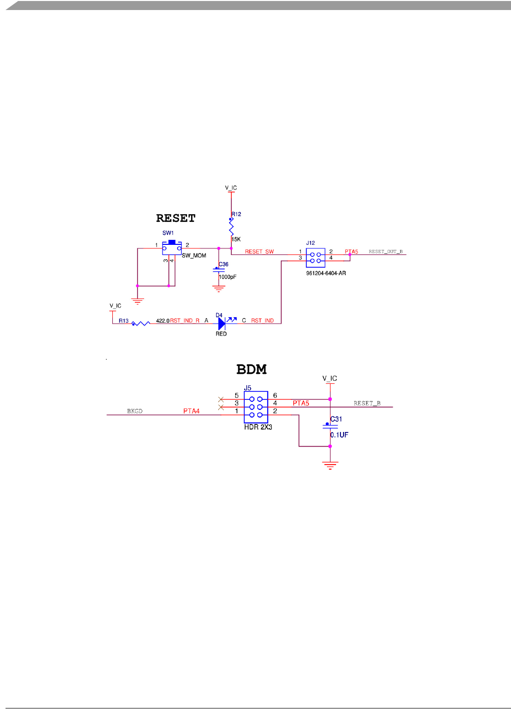
3.3 Reset and BDM Debug Port
The reset circuit and BDM port connector are shown in Figure 3-7. See Figure 3-1 for switch and header
locations.
• Reset switch SW1 is active low and provides a hardware reset to the MC12311 MCU die and can
also provide a RESET to the radio die by adding a jumper to J7. The Reset circuit also includes an
LED for monitoring purposes.
• The 6-pin BDM 2x3 header J5 is provided to connect the MC1213x serial debug port to a standard
HC9S08 debug module.
Figure 3-7. 12311-MRB Reset Switch and BDM Port
12311-MRB
12311 Development Hardware Reference Manual, Rev. 1
Freescale Semiconductor 3-9
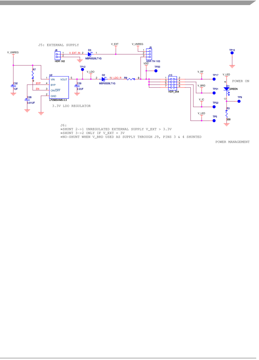
3.3.1 Power Management
The 12311-MRB power management circuit is shown in Figure 3-8.
Figure 3-8. 12311-MRB Power Management Circuit
Power to the 12311-MRB can be configured in several ways and the circuit has the following features:
• Board can be supplied through the IO headers (V_BRD)
• Board can be supplied from an external DC supply (J6)
— The external supply can be unregulated (V_UNREG) and make use of the onboard 3.3 V LDO
regulator
— The external supply voltage can be used directly without use of the LDO
• 8-Pin 2x4 header J13 provides means to supply current to various board components and also
measure current if desired
• Green LED D1 is available as a power indicator.
Table 3-2 shows the header configuration information for the various power supply modes.
NOTE
• The Freescale TWR-RF development boards generate the system power
supply on the motherboard and supply the voltage to the 12311-MRB
through the V_BRD pin of Headers J2 and J3. In this mode, the current
flows to the 12311-MRB through the pins.
• If an external supply is used via 12311-MRB header J5, current flows to
the motherboard through the V_BRD pin of Headers J2 and J3. THE
MOTHERBOARD SUPPLY SHOULD NOT BE USED.
• In all modes, the IO voltage supply of peripherals on a motherboard
must be the same voltage as V_BRD, which is also the voltage applied
to the IC MC1213x.
12311-MRB
12311 Development Hardware Reference Manual, Rev. 1
3-10 Freescale Semiconductor
Header J13 provides means to disable different sub-circuits or measure current and connections are
described in Table 3-3. Current measurements can be made by inserting a current meter in place of a
designated jumper.
Table 3-2. 12311-MRB Power Configurations
Mode Voltage
Range
External
Source
J6
Ext Mode
Select
J9
Current Enable
J13 Description
Source V_BRD 2.7 - 3.6 V1
1The MC12311 can run as low as 1.8 V
Not used Not used - all
pins open
Short Pins 3-4 -
short other desired
supplies
Normal Operation -
The 12311-MRB main supply is
supplied by the motherboard
through the J15 and J14 Headers
External Source
- Using LDO
3.5 - 16 V Connected -
supplies
DC Voltage
Short Pins 1-2 Short pins for all
desired supplies
External voltage w/regulation -
• Input range is set by the LDO
regulator.
• 3.3 V is supplied to 12311-MRB;
do not use motherboard supply
• J14 and J15 Headers supply
voltage to V_BRD pins when J13,
Pins 3-4 are shorted
External Source
- Not Using LDO
2.7 - 3.6 V Connected -
supplies
DC Voltage
Short Pins 2-3 Short pins for all
desired supplies
External voltage w/o regulation -
• Input range is set by the onboard
circuitry
• 2.7 - 3.3 V is supplied to
12311-MRB
• J14 and J15 Headers supply
voltage to V_BRD pins
Table 3-3. Power Distribution Header J13
Supply
Designation
Header
Pins Description
V_RF 1 - 2 Supply voltage to MC12311 -Radio die
• Normally jumpered
• Supplies only the MC12311 Radio die
Normally always same voltage as V_BRD
V_BRD 3 - 4 Supply voltage connected to IO Connectors J2 and J3 -
• This supplies J2 and J3 if an external MRB supply is used
• This voltage supplies the MRB if the motherboard is the main power
• This connection is normally always jumpered
V_IC 5 - 6 Supply voltage to MC12311 -MCU die
• Normally jumpered
• Supplies only the MC12311 MCU die
• Normally always same voltage as V_BRD
V_LED 7 - 8 Supply voltage to power indicator LED
• Jumper to use indicator or IR blaster
• Leave open for lowest power
12311-MRB
12311 Development Hardware Reference Manual, Rev. 1
Freescale Semiconductor 3-11
3.3.2 IO Connectors J2 and J3
The two IO connectors J14 and J15 are standard 100 mil pin headers mounted on the back (non-component
side) of the 12311-MRB.The primary header J15 is 20-pin and the secondary header J14 is 18-pin, and
they are mounted physically in such a manner as to prevent reverse insertion of the 12311-MRB into a
motherboard receptacle (see Figure 3-2). When the TWR-RF, 1323x-RCM or 1323x-REM or custom
motherboard is plugged into these connectors, they allow access to MC12311 MCU GPIO.
• V_BRD is the connector supply voltage.
— Depending on power supply configuration, this voltage may supply the 12311-MRB from the
motherboard or the 12311-MRB may supply this voltage to the motherboard. See Section 3.3.1,
“Power Management”.
— Peripherals IO to the MC12311 and the MC12311 supply should use this same voltage
NOTE
The TWR-RF, 1323x-RCM and 1323x-REM and 12311-MRB are supplied
configured for the motherboard to supply main power.
• Some of the GPIO are shared with onboard devices. Check for the 12311-MRB schematic and
Table 3-4 and Table 3-5 for any conflict.
• BDM port signal PTA4/BKGD is NOT connected to the IO headers to prevent possible interference
with the debug port.
Table 3-4. 20 Pin Connector
Header Pin
Number MC12311 Pin Name Description
1 V_BRD VDD supply to module
2NC
3 GND Module ground
4NC
5 PTB1/TXD UART TXD input to MCU
6NC
7 PTB0/RXD UART RXD Output from MCU
8NC
9 PTA7 GPIO / Timer IO
10 RESET MCU Reset
11 PTA2/SDA I2C Bus data signal (SDA)
12 PTD4/KBI2P4 UART flow control RTS input into MCU (implemented in Freescale software)
13 PTA3/SCL I2C Bus clock signal (SCL)
14 PTD3/KBI2P UART flow control CTS output from MCU (implemented in Freescale software)
15 GND Module ground
16 DIO5/CLKOUT Reference Crystal Oscillator
12311-MRB
12311 Development Hardware Reference Manual, Rev. 1
3-12 Freescale Semiconductor
17 PTA0/KBI1P0 Port A Bit 0 / KBI1 Input Bit 0
18 PTA1/KBI1P1 Port A Bit 1 / KBI1 Input Bit 1
19 PTB2/KBI1P2 Port B Bit 2 / KBI1 Input Bit 2
20 PTB3/KBI1P3 Port B Bit 3 / KBI1 Input Bit 3
Table 3-5. 18 Pin Connector
Header Pin
Number MC12311 Pin Name Description
1 V_BRD VDD supply to module
2 PTB7/EXTAL Port B Bit 7 - signal shared with 32.768 kHz oscillator
3 PTB6/XTAL_32K Port B Bit 6 - signal shared with 32.768 kHz oscillator
4 GND Module Ground
5 PTB5/TPM1CH1 Port B Bit 5
6 PTB4/TPM2CH1 Port B Bit 4
7 PTC3/TPM3CH3 Port C Bit 3
8 PTC2/TPM3CH2 Port C Bit 2
9 PTC1/TPM3CH1 Port C Bit 1
10 PTD2 Port D Bit 2
11 PTA6/TPM1CH2 Port A Bit 6
12 PTC7 Port C Bit 7
13 PTC6 Port C Bit 6
14 PTC5/TPM3CH5 Port C Bit 5
15 PTC4/TPM3CH4 Port C Bit 4
16 DIO2 Transceiver GPIO Bit 2
17 DIO3 Transceiver GPIO Bit 3
18 GND Module ground
Table 3-4. 20 Pin Connector (continued)
Header Pin
Number MC12311 Pin Name Description
12311-MRB
12311 Development Hardware Reference Manual, Rev. 1
3-14 Freescale Semiconductor
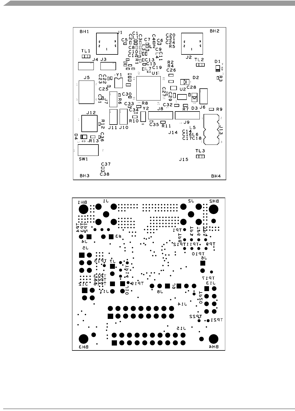
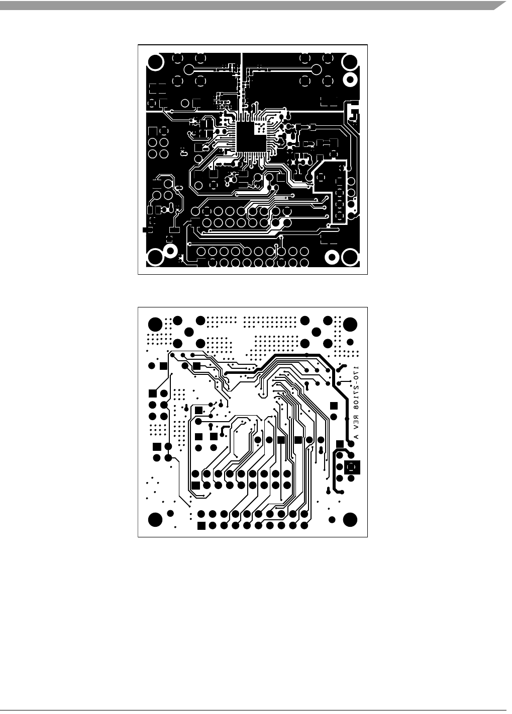
Figure 3-10. Modular Reference Board PCB Component Location (Top View)
Figure 3-11. Modular Reference Board PCB Test Points
12311-MRB
12311 Development Hardware Reference Manual, Rev. 1
Freescale Semiconductor 3-15
Figure 3-12. Modular Reference Board PCB Layout (Top View)
Figure 3-13. Modular Reference Board PCB Layout (Bottom View)

12311-MRB
12311 Development Hardware Reference Manual, Rev. 1
3-16 Freescale Semiconductor
3.4.1 Bill of Materials
The following table details the bill of materials.
Table 3-6. Bill of Materials
Item Qty Reference Value Description Mfg. Name Mfg. Part Number
1 4 BH1,BH2,B
H3,BH4
125 NON-PLATED MOUNTING HOLE
125 DRILL / 160 KEEPOUT NO
PART TO ORDER
2 3 C1,C7,C23
(DNP)
10PF CAP CER 10PF 50V 5% C0G 0402 Avx 04025A100JAT2A
3 2 C5,C6 10PF CAP CER 10PF 50V 5% C0G 0402 Avx 04025A100JAT2A
4 10 C14,C19,C
20,C21,C2
4,C30,C31,
C33,C37,C
38
0.1UF CAP CER 0.1UF 16V 10% X7R
0402
Kemet C0402C104K4RAC
5 2 C16,C18 220PF CAP CER 220PF 50V 5% C0G
0402
Kemet C0402C221J5GAC
6 3 C17,C27,C
28
0.01UF CAP CER 0.01UF 50V 10% X7R
0402
Murata GCM155R71H103KA55D
7 2 C22,C25 11PF CAP CER 11PF 50V 5% C0G 0402 Murata GRM1555C1H110JZ01D
8 2 C34,C35 12PF CAP CER 12PF 50V 5% C0G 0402 Murata GRM1555C1H120JZ01D
9 1 C26 10UF CAP CER 10UF 10V 10% X5R
0805
Murata GRM21BR61A106KE19_
10 1 C29 2.2UF CAP CER 2.2UF 10V 10% X7R
0603
Murata GRM188R71A225KE15D
11 1 C32 1UF CAP CER 1.0UF 10V 10% X7R
0603
Murata GRM188R71A105KA61D
12 1 C36 1000pF CAP CER 1000PF 50V 5% C0G
0402
Murata GRM1555C1H102JA01D
13 1 D1 GREEN LED GRN SGL 30MA SMT 0805 Lite On LTST-C171KGKT
14 2 D2,D3 MBR0520LT1G DIODE SCH 0.5A 20V SOD-123 On Semiconductor MBR0520LT1G
15 1 D4 RED LED RED CLEAR SGL 30MA SMT
0805
Lite On LTST-C171KRKT
16 2 J1,J2 CON_1_SMA CON 1 COAX SMA SKT TH --
376H AU
Samtec SMA-J-P-H-ST-TH1
17 6 J3,J4,J6,J7
,J10,J11
HDR 1X2 HDR 1X2 TH 100MIL SP 330H SN
115L
Samtec TSW-102-07-T-S
18 1 J5 HDR 2X3 HDR 2X3 TH 100MIL CTR 335H
AU 95L
Samtec TSW-103-07-S-D
19 2 J8,J9 HDR TH 1X3 HDR 1X3 TH 100MIL SP 339H AU
100L
Samtec TSW-103-07-G-S

12311-MRB
12311 Development Hardware Reference Manual, Rev. 1
Freescale Semiconductor 3-17
20 1 J12 961204-6404-A
R
HDR 2X2 TH 100MIL CTR 323H
AU 130L
3m 961204-6404-AR
21 1 J13 HDR_2X4 HDR 2X4 TH 100MIL CTR 330H
AU 100L
Samtec TSW-104-07-S-D
22 1 J14 HDR 2X9 HDR 2X9 TH 100MIL CTR 330H
AU
Samtec TSW-109-07-S-D
23 1 J15 HDR_10X2 HDR 2X10 TH 100MIL CTR 330H
AU 100L
Samtec TSW-110-07-S-D
24 1 L6 33nH IND -- 0.033UH@100MHZ 200MA
5% 0402
Toko Inc. LL1005-FHL33NJ
25 2 R2,R4 4.7K RES MF 4.7K 1/10W 5% 0603 Vishay Intertechnology CRCW06034K70JNEA
26 1 R3 330 RES MF 330 OHM 1/16W 5% 0402 Vishay Intertechnology CRCW0402330RJNED
27 6 R5,R7,R8,
R9,R10,R1
1
0 RES MF ZERO OHM 1/10W --
0603
Vishay Intertechnology CRCW06030000Z0EA
28 1 R6 10.0K RES MF 10.0K 1/16W 1% 0402 Vishay Intertechnology CRCW040210K0FKED
29 1 R12 15K RES MF 15K 1/16W 5% 0402 Vishay Intertechnology CRCW040215K0JNED
30 1 R13 422 RES MF 422 OHM 1/10W 1%
0603
Yageo America RC0603FR-07422RL
31 1 SW1 SW_MOM SW SPST MOM PB 50MA 12V
SMT
Alps Electric (Usa) Inc. SKQYPDE010
32 3 TL1,TL2,TL
3
TESTLOOP TEST POINT PAD SIZE 3.4MM X
1.8MM SMT
Keystone Electronics 5015
33 22 TP1,TP2,T
P3,TP4,TP
5,TP6,TP7,
TP8,TP9,T
P10,TP11,
TP12,TP13
,TP14,TP1
5,TP16,TP
17,TP18,T
P19,TP20,
TP21,TP22
TPAD_040 TEST POINT PAD 40MIL DIA SMT,
NO PART TO ORDER
Notacomponent NOTACOMPONENT
34 1 U1 MC12311 IC MCU 8BIT 32KB FLASH 2KB
RAM 50MHZ 1.8-3.6V LGA60
Freescale
Semiconductor
MC12311
35 1 U2 LP2985AIM5-3
.3
IC VREG LDO 3.3V 150MA
3.8-16V SOT-23-5
National
Semiconductor
LP2985AIM5-3.3/NOPB
36 1 Y1 32MHZ XTAL 32MHZ 9PF -- SMT
3.2X2.5MM
Ndk EXS00A-CS02368
37 1 Y2 32.768KHZ XTAL 32.768KHZ SMT ROHS
COMPLIANT
Epson Electronics FC-135 32.7680KA-A3
Table 3-6. Bill of Materials
Item Qty Reference Value Description Mfg. Name Mfg. Part Number
12311-MRB
12311 Development Hardware Reference Manual, Rev. 1
3-18 Freescale Semiconductor
1 1 C2 3.3pf CAP CER 3.3PF 25V 0.1PF --
0402
AVX 04023J3R3BBSTR
2 1 C4 5.6PF CAP CER 5.6PF 50V +/-0.25PF
C0G CC0402
MURATA GJM1555C1H5R6CB01D
3 2 C3,C9 6.8PF CAP CER 6.8PF 50V 0.5PF C0G
0402
MURATA GRM1555C1H6R8DZ01J
4 1 C10 47PF CAP CER 47PF 50V 5% C0G 0402 CAL-CHIP GMC04CG470J50NT-LF
5 1 C13 8.2PF CAP CER 8.2PF 50V 0.25PF C0G
0402
AVX 04025A8R2CAT2A
6 1 C15 4.7PF CAP CER 4.7PF 50V 0.25PF C0G
0402
MURATA GRM1555C1H4R7CA01D
7 2 C8,C11 10PF CAP CER 10PF 50V 5% C0G 0402 AVX 04025A100JAT2A
8 1 C12 10PF CAP CER 10PF 50V 5% C0G 0402 AVX 04025A100JAT2A
9 2 L1,L3 5.6NH IND AIR 5.6NH@100MHZ 300MA
0.3NH 0402
muRata LQG15HN5N6S02D
10 2 L2,L4 0.0068UH IND -- 0.0068UH@100MHZ
300MA 5% 0402
MURATA LQG15HS6N8J02D
11 1 L7 0.0039UH IND -- 0.0039UH@100MHZ
300MA +/-0.3NH 0402
MURATA LQG15HN3N9S02D
12 1 L5 33nH IND -- 0.033UH@100MHZ 200MA
5% 0402
TOKO INC. LL1005-FHL33NJ
13 1 R1 (L9 in
433 BOM)
0 RES MF ZERO OHM 1/10W --
0402
Panasonic ERJ-2GE0R00X
Table 3-6. Bill of Materials
Item Qty Reference Value Description Mfg. Name Mfg. Part Number

12311 Development Hardware Reference Manual, Rev. 1
Freescale Semiconductor 4-1
Chapter 4
PCB Manufacturing Specifications
This chapter provides the specifications used to manufacture the MC12311 Development hardware printed
circuit board (PCB) described in this manual.
The MC12311 Development hardware PCBs must comply with the following:
• The PCB must comply with Perfag10/3C (http://www.perfag.dk/Uk/ukindex.htm)
• The PCB manufacturer’s logo is required
• The PCB production week and year code is required
— The manufacturer’s logo and week/year code must be stamped on the back of the PCB solder
mask
— The PCB manufacturer can not insert text on the PCB either in copper or in silkscreen without
written permission from Freescale Semiconductor, Inc.
• The required Underwriter’s Laboratory (UL) Flammability Rating
— The level is 94V-0 (http://www.ul.com/plastics/flame.html)
— The UL information must be stamped on the back of the PCB solder mask
NOTE
• A complete set of design files is available for the 12311 Development
hardware at the Freescale web site (http:www.freescale.com/802154)
under reference designs. It is recommended that this design or one of a
number of other reference designs be used as a starting point for a
custom application.
• The Freescale IEEE 802.15.4 / ZigBee Package and Hardware Layout
Considerations Reference Manual, (ZHDCRM) is also available at the
same web site to provide additional design guidance.
4.1 Single PCB Construction
This section describes individual PCB construction details.
• The MC12311 PCB is a four-layer, multi layer designs
• The PCBs contains no blind, buried, or micro vias
• PCB data:
— MC12311 Size: Approximately 51 x 51mm (2.01 x 2.01 inches)
— MC12311 Final thickness (Cu/Cu): 0.34 mm (0.8 inches) +/- 10% (excluding solder mask)
The following table defines some of the layers of the completed PCB. The artwork identification refers to
the name of the layer in commonly used terms.
PCB Manufacturing Specifications
12311 Development Hardware Reference Manual, Rev. 1
4-2 Freescale Semiconductor
NOTE
The MC12311 contains sub 1 GHz RF circuitry. As a result, RF component
placement, line geometries and layout, and spacing to the ground plane are
critical parameters. As a result, BOARD STACKUP GEOMETRY IS
CRITICAL. Dielectric and copper thicknesses and spacing must not be
changed; follow the stackup (see Figure 4-1) information is provided with
the reference design.
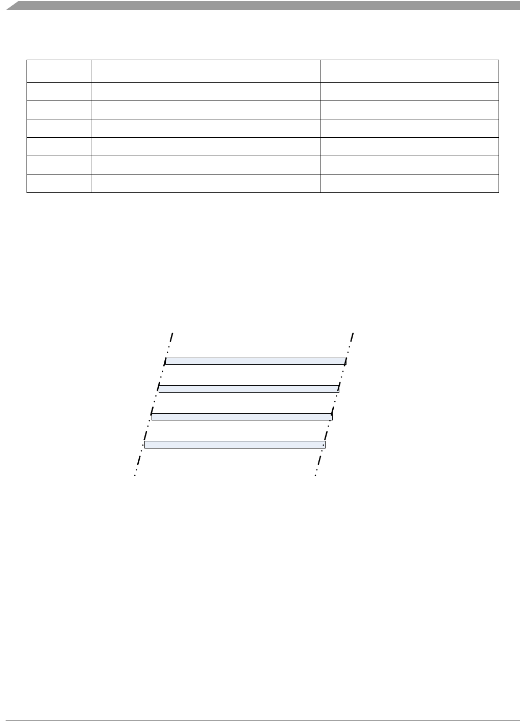
Figure 4-1. MC12311 PCB Stackup Cross-Section (Four Layer)
• Solder mask is required
• Silk screen is required
4.2 Panelization
The panel size can be negotiated depending on production volume.
4.3 Materials
The PCB composite materials must meet the following requirements:
• Laminate - The base laminate material (laminate) must be FR4. If the laminate material were
changed the RF electrical characteristics may change and degrade RF performance.
Table 4-1. MC12311 Layer by Layer Overview
Layer Artwork Identification File Name
1 Silkscreen Top SILK_TOP.art
2 Top Layer Metal TOP.art
3 Ground Layer GND.art
4 Power Layer PWR.art
5 Bottom Layer Metal BOTTOM.art
6 Silkscreen Bottom SILK_BOTTOM.art
Dielectric
Dielectric
Dielectric
Metal 1
Metal 2
Metal 3
Metal 4

PCB Manufacturing Specifications
12311 Development Hardware Reference Manual, Rev. 1
Freescale Semiconductor 4-3
• Copper Foil -
— Top and Bottom copper layers must be 1 oz. copper
— Interior layers must be 1/2 oz. copper
• Plating - All pad plating must be Hot Air Levelling (HAL)
4.4 Solder Mask
The solder mask must meet the following requirements:
• Solder mask type: Liquid Film Electra EMP110 or equivalent
• Solder mask thickness: 10 – 30 µm
4.5 Silk Screen
The silk screen must meet the following requirements:
• Silkscreen color: White
• Silkscreen must be applied after application of solder mask if solder mask is required
• The silkscreen ink must not extend into any plated-thru-holes
• The silk screen must be clipped back to the line of resistance
4.6 Electrical PCB Testing
• All PCBs must be 100 percent tested for opens and shorts
• Impedance Measurement - An impedance measurement report is not mandatory
4.7 Packaging
Packaging for the PCBs must be the following requirements:
• Finished PCBs must remain in panel
• Finished PCBs must be packed in plastic bags that do not contain silicones or sulphur materials.
These materials can degrade solderability.
4.8 Hole Specification/Tool Table
See the ncdrill-1-4.tap file included with the Gerber files and the FAB-23451.pdf file.

PCB Manufacturing Specifications
12311 Development Hardware Reference Manual, Rev. 1
4-4 Freescale Semiconductor
4.9 File Description
Files included with the download include Design, Gerber and PDF files.
Gerber files are RS-374x format. Not all files included with the Gerber files are for PCB manufacturing.
PDF files included are:
• FAB-27108.pdf — Board fabrication drawing
• GRB-27108.zip — Metal layers, solder mask, solder paste and silk screen
• SPF-27108.pdf — Schematic
Design files are in Allegro format with OrCAD schematic capture.