Freescale Semiconductor 1322X-LPB 1322x-LPB User Manual
Freescale Semiconductor, Inc. 1322x-LPB
Users Manual Rev 2

Document Number: 1322xLPBRM
Rev. 1.1
07/2008
1322x-Low Power Board
(1322x-LPB)
Reference Manual

How to Reach Us:
Home Page:
www.freescale.com
E-mail:
support@freescale.com
USA/Europe or Locations Not Listed:
Freescale Semiconductor
Technical Information Center, CH370
1300 N. Alma School Road
Chandler, Arizona 85224
+1-800-521-6274 or +1-480-768-2130
support@freescale.com
Europe, Middle East, and Africa:
Freescale Halbleiter Deutschland GmbH
Technical Information Center
Schatzbogen 7
81829 Muenchen, Germany
+44 1296 380 456 (English)
+46 8 52200080 (English)
+49 89 92103 559 (German)
+33 1 69 35 48 48 (French)
support@freescale.com
Japan:
Freescale Semiconductor Japan Ltd.
Headquarters
ARCO Tower 15F
1-8-1, Shimo-Meguro, Meguro-ku,
Tokyo 153-0064, Japan
0120 191014 or +81 3 5437 9125
support.japan@freescale.com
Asia/Pacific:
Freescale Semiconductor Hong Kong Ltd.
Technical Information Center
2 Dai King Street
Tai Po Industrial Estate
Tai Po, N.T., Hong Kong
+800 2666 8080
support.asia@freescale.com
For Literature Requests Only:
Freescale Semiconductor Literature Distribution Center
P.O. Box 5405
Denver, Colorado 80217
1-800-521-6274 or 303-675-2140
Fax: 303-675-2150
LDCForFreescaleSemiconductor@hibbertgroup.com
Information in this document is provided solely to enable system and software implementers to use
Freescale Semiconductor products. There are no express or implied copyright licenses granted
hereunder to design or fabricate any integrated circuits or integrated circuits based on the information
in this document.
Freescale Semiconductor reserves the right to make changes without further notice to any products
herein. Freescale Semiconductor makes no warranty, representation or guarantee regarding the
suitability of its products for any particular purpose, nor does Freescale Semiconductor assume any
liability arising out of the application or use of any product or circuit, and specifically disclaims any
and all liability, including without limitation consequential or incidental damages. “Typical”
parameters that may be provided in Freescale Semiconductor data sheets and/or specifications can
and do vary in different applications and actual performance may vary over time. All operating
parameters, including “Typicals”, must be validated for each customer application by customer’s
technical experts. Freescale Semiconductor does not convey any license under its patent rights nor
the rights of others. Freescale Semiconductor products are not designed, intended, or authorized for
use as components in systems intended for surgical implant into the body, or other applications
intended to support or sustain life, or for any other application in which the failure of the Freescale
Semiconductor product could create a situation where personal injury or death may occur. Should
Buyer purchase or use Freescale Semiconductor products for any such unintended or unauthorized
application, Buyer shall indemnify and hold Freescale Semiconductor and its officers, employees,
subsidiaries, affiliates, and distributors harmless against all claims, costs, damages, and expenses,
and reasonable attorney fees arising out of, directly or indirectly, any claim of personal injury or death
associated with such unintended or unauthorized use, even if such claim alleges that Freescale
Semiconductor was negligent regarding the design or manufacture of the part.
ARM is the registered trademark of ARM Limited. ARM7TDMI-S is the trademark of ARM Limited.
Freescale™ and the Freescale logo are trademarks of Freescale Semiconductor, Inc. All other
product or service names are the property of their respective owners.
© Freescale Semiconductor, Inc. 2005, 2006, 2007, 2008. All rights reserved.

1322x-LPB Reference Manual, Rev. 1.1
Freescale Semiconductor i
Contents
About This Book
Audience . . . . . . . . . . . . . . . . . . . . . . . . . . . . . . . . . . . . . . . . . . . . . . . . . . . . . . . . . . . . . . . . . . . . iii
Organization . . . . . . . . . . . . . . . . . . . . . . . . . . . . . . . . . . . . . . . . . . . . . . . . . . . . . . . . . . . . . . . . . iii
Revision History . . . . . . . . . . . . . . . . . . . . . . . . . . . . . . . . . . . . . . . . . . . . . . . . . . . . . . . . . . . . . . iii
Chapter 1
Safety Information
1.1 FCC Guidelines. . . . . . . . . . . . . . . . . . . . . . . . . . . . . . . . . . . . . . . . . . . . . . . . . . . . . . . . . . . . . . 1-1
1.2 FCC Labeling . . . . . . . . . . . . . . . . . . . . . . . . . . . . . . . . . . . . . . . . . . . . . . . . . . . . . . . . . . . . . . . 1-1
1.2.1 47 C.F.R. Sec. 15.21 . . . . . . . . . . . . . . . . . . . . . . . . . . . . . . . . . . . . . . . . . . . . . . . . . . . . . . . 1-1
1.2.2 47 C.F.R. Sec.15.105(b) . . . . . . . . . . . . . . . . . . . . . . . . . . . . . . . . . . . . . . . . . . . . . . . . . . . . 1-2
1.2.3 47 C.F.R. Sec.15.203 . . . . . . . . . . . . . . . . . . . . . . . . . . . . . . . . . . . . . . . . . . . . . . . . . . . . . . 1-2
1.3 Regulatory Approval For Canada. . . . . . . . . . . . . . . . . . . . . . . . . . . . . . . . . . . . . . . . . . . . . . . . 1-2
1.4 Disposal Instructions. . . . . . . . . . . . . . . . . . . . . . . . . . . . . . . . . . . . . . . . . . . . . . . . . . . . . . . . . . 1-2
Chapter 2
1322x-LPB Module Overview and Description
2.1 Introduction. . . . . . . . . . . . . . . . . . . . . . . . . . . . . . . . . . . . . . . . . . . . . . . . . . . . . . . . . . . . . . . . . 2-1
2.2 Features. . . . . . . . . . . . . . . . . . . . . . . . . . . . . . . . . . . . . . . . . . . . . . . . . . . . . . . . . . . . . . . . . . . . 2-2
2.3 Board Level Specifications. . . . . . . . . . . . . . . . . . . . . . . . . . . . . . . . . . . . . . . . . . . . . . . . . . . . . 2-3
Chapter 3
System Overview and Functional Block Descriptions
3.1 System Block Diagram . . . . . . . . . . . . . . . . . . . . . . . . . . . . . . . . . . . . . . . . . . . . . . . . . . . . . . . . 3-1
3.2 Design Overview . . . . . . . . . . . . . . . . . . . . . . . . . . . . . . . . . . . . . . . . . . . . . . . . . . . . . . . . . . . . 3-1
3.2.1 1322x-LPB Form Factor. . . . . . . . . . . . . . . . . . . . . . . . . . . . . . . . . . . . . . . . . . . . . . . . . . . . 3-3
3.3 RF 2.4 GHz ISM Band radio design. . . . . . . . . . . . . . . . . . . . . . . . . . . . . . . . . . . . . . . . . . . . . . 3-4
3.4 Power Sources. . . . . . . . . . . . . . . . . . . . . . . . . . . . . . . . . . . . . . . . . . . . . . . . . . . . . . . . . . . . . . . 3-4
3.4.1 External DC Source . . . . . . . . . . . . . . . . . . . . . . . . . . . . . . . . . . . . . . . . . . . . . . . . . . . . . . . 3-4
3.4.2 Battery Sources. . . . . . . . . . . . . . . . . . . . . . . . . . . . . . . . . . . . . . . . . . . . . . . . . . . . . . . . . . . 3-5
3.4.3 Optional Use of MC1322x Buck Regulator . . . . . . . . . . . . . . . . . . . . . . . . . . . . . . . . . . . . . 3-6
3.5 Clock Sources . . . . . . . . . . . . . . . . . . . . . . . . . . . . . . . . . . . . . . . . . . . . . . . . . . . . . . . . . . . . . . . 3-7
3.5.1 Reference Oscillator (24 MHz nominal) . . . . . . . . . . . . . . . . . . . . . . . . . . . . . . . . . . . . . . . 3-7
3.5.2 32.768 kHz Crystal Oscillator . . . . . . . . . . . . . . . . . . . . . . . . . . . . . . . . . . . . . . . . . . . . . . . 3-8
3.6 FLASH Memory Recovery Jumpers and Erase . . . . . . . . . . . . . . . . . . . . . . . . . . . . . . . . . . . . . 3-8
3.7 Low Power Operation. . . . . . . . . . . . . . . . . . . . . . . . . . . . . . . . . . . . . . . . . . . . . . . . . . . . . . . . . 3-9
3.7.1 Switched VCC for Peripheral Functions . . . . . . . . . . . . . . . . . . . . . . . . . . . . . . . . . . . . . . . 3-9
3.7.2 Measuring Current . . . . . . . . . . . . . . . . . . . . . . . . . . . . . . . . . . . . . . . . . . . . . . . . . . . . . . . 3-10
3.7.3 Other Low Power Considerations. . . . . . . . . . . . . . . . . . . . . . . . . . . . . . . . . . . . . . . . . . . . 3-10
3.8 User Interfaces . . . . . . . . . . . . . . . . . . . . . . . . . . . . . . . . . . . . . . . . . . . . . . . . . . . . . . . . . . . . . 3-11
3.8.1 LEDs, Switches, and Reset. . . . . . . . . . . . . . . . . . . . . . . . . . . . . . . . . . . . . . . . . . . . . . . . . 3-11
3.8.2 ADC Voltage References . . . . . . . . . . . . . . . . . . . . . . . . . . . . . . . . . . . . . . . . . . . . . . . . . . 3-11

1322x-LPB Reference Manual, Rev. 1.1
ii Freescale Semiconductor
3.8.3 ARM JTAG Debug Interface Connector . . . . . . . . . . . . . . . . . . . . . . . . . . . . . . . . . . . . . . 3-12
3.8.4 GPIO Connector . . . . . . . . . . . . . . . . . . . . . . . . . . . . . . . . . . . . . . . . . . . . . . . . . . . . . . . . . 3-12
3.8.5 UART Connector . . . . . . . . . . . . . . . . . . . . . . . . . . . . . . . . . . . . . . . . . . . . . . . . . . . . . . . . 3-13
3.8.6 Jumper Selection. . . . . . . . . . . . . . . . . . . . . . . . . . . . . . . . . . . . . . . . . . . . . . . . . . . . . . . . . 3-14
Chapter 4
Schematic, Board Layout, and Bill of Materials

1322x-LPB Reference Manual, Rev. 1.1
Freescale Semiconductor iii
About This Book
This manual describes Freescale’s 1322x-LPB evaluation board. The 1322x-LPB contains a Freescale
third-generation, low power, 2.4 GHz radio frequency transceiver, with 32-bit ARM7 core based MCU,
hardware acceleration for both the IEEE Standard 802.15.4 MAC and AES security, and a full set of MCU
peripherals into a 99-pin LGA Platform-in-Package (PiP).
Audience
This manual is intended for system designers.
Organization
This document is organized into 4 chapters.
Chapter 1 Safety Information — Describes that any modifications to this product may
violate the rules of the Federal Communications Commission and make operation
of the product unlawful.
Chapter 2 1322x-LPB Module Overview and Description — Introduces the 1322x-LPB,
which is an IEEE 802.15.4 compliant wireless node based on the Freescale
MC1322x device.
Chapter 3 System Overview and Functional Block Descriptions — This section provides an
overview of the 1322x-LPB and its block diagram.
Chapter 4 Schematic and Bill of Material — Contains the schematic, board layout, and bill
of material (BOM).
Revision History
The following table summarizes revisions to this document since the previous release (Rev 1.0).
SRevision History
Location Revision
Chapter 1 Updated FCC information.

1322x-LPB Reference Manual, Rev. 1.1
iv Freescale Semiconductor
Definitions, Acronyms, and Abbreviations
The following list defines the acronyms and abbreviations used in this document.
ADC Analog to Digital Converter
AES Advanced Encryption Standard
ARM Advanced RISC Machine
CTS Clear to Send
DAC Digital to Analog Converter
DMA Direct Memory Access
I2C Inter-Integrated Circuit is a multi-master serial computer bus
ISM Industrial Scientific Medical 2.4 GHz radio frequency band
JTAG Joint Test Action Group
LGA Land Grid Array
MAC Media Access Controller
MCU Microcontroller Unit
NEXUS An embedded processor development tool interface that helps design engineers
identify software and hardware-level issues.
SN Sensor Node
pcb Printed circuit board
PiP Platform in Package
PWM Pulse-width modulation
RTS Request to Send
SMA Connector Sub Miniature version “A” connector
SPI Serial Peripheral Interface
SSI Synchronous Serial Interface
TACT Switch A switch that provides a slight “snap” or “click” to the user to indicate function.
TELCO Telephone Company
USB Universal Serial Bus
VCP Virtual Com Port

1322x-LPB Reference Manual, Rev. 1.0
Freescale Semiconductor 1-1
Chapter 1
Safety Information
1.1 FCC Guidelines
This equipment is for use by developers for evaluation purposes only and must not be incorporated into
any other device or system. This device may not be sold to the general public. Integrators will be
responsible for reevaluating the end product (including the transmitter) and obtaining a separate FCC
authorization.
FCC approval of this device only covers the original configuration of this device as supplied. Any
modifications to this product, including changes shown in this manual, may violate the rules of the Federal
Communications Commission and make operation of the product unlawful. NOTE:The statement above
applies also to the Industry Canada Approval
1.2 FCC Labeling
FCC labels are physically located on the back of the board.
1.2.1 47 C.F.R. Sec. 15.21
This equipment has been tested and found to comply with the limits for a Class B digital device, pursuant
to part 15 of the FCC Rules. These limits are designed to provide reasonable protection against harmful
interference in a residential installation. This equipment generates, uses and can radiate radio frequency
energy and, if not installed and used in accordance with the instructions, may cause harmful interference
to radio communications. However, there is no guarantee that interference will not occur in a particular
installation. If this equipment does cause harmful interference to radio or television reception, which can
be determined by turning the equipment off and on, the user is encouraged to try to correct the interference
by one or more of the following measures:
• Reorient or relocate the receiving antenna.
• Increase the separation between the equipment and receiver.
• Connect the equipment into an outlet on a circuit different from that to which the receiver is
connected.
• Consult the dealer or an experienced radio/TV technician for help.

Safety Information
1322x-LPB Reference Manual, Rev. 1.0
1-2 Freescale Semiconductor
1.2.2 47 C.F.R. Sec.15.105(b)
This equipment complies with FCC radiation exposure limits set forth for an uncontrolled environment.
The antenna(s) used for this equipment must be installed to provide a separation distance of at least 8
inches (20cm) from all persons.
This device complies with Part 15 of the FCC Rules. Operation is subject to the following three
conditions:
1. This device may not cause harmful interference.
2. This device must accept any interference received, including interference that may cause undesired
operation.
3. This device is susceptible to electrostatic discharge (ESD) and surge phenomenon.
1.2.3 47 C.F.R. Sec.15.203
An intentional radiator shall be designed to ensure that no antenna other than that furnished by the
responsible party shall be used with the device. The use of a permanently attached antenna or of an
antenna that uses a unique coupling to the intentional radiator shall be considered sufficient to comply with
the provisions of this Section. The manufacturer may design the unit so that a broken antenna can be
replaced by the user, but the use of a standard antenna jack or electrical connector is prohibited. This
requirement does not apply to carrier current devices or to devices operated under the provisions of
Sections 15.211, 15.213, 15.217, 15.219, or 15.221. Further, this requirement does not apply to intentional
radiators that must be professionally installed, such as perimeter protection systems and some field
disturbance sensors, or to other intentional radiators which, in accordance with Section 15.31(d), must be
measured at the installation site. However, the installer shall be responsible for ensuring that the proper
antenna is employed so that the limits in this Part are not exceeded.
1.3 Regulatory Approval For Canada
This Class B digital apparatus complies with Canadian ICES-003 and RSS 210, Issue 7.
Cet appareil numérique de la classe B est conforme à la norme NMB-003 du Canada. NOTE: Section 1.1
of this manual also applies to the Industry Canada Approval
1.4 Disposal Instructions
This product may be subject to special disposal requirements. For product disposal instructions, refer to
www.freescale.com/productdisposal.
1322x-LPB Reference Manual, Rev. 1.1
Freescale Semiconductor 2-1
Chapter 2
1322x-LPB Module Overview and Description
2.1 Introduction
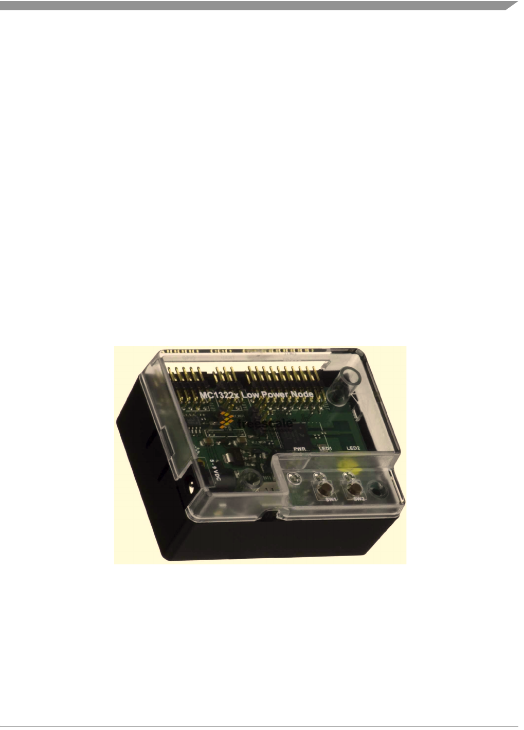
The 1322x-LPB is an IEEE 802.15.4 compliant wireless node based on the Freescale MC1322x device.
The heart of the MC1322x USB module is Freescale’s MC1322x 99-pin LGA Platform-in-Package (PiP)
solution that can be used for wireless applications ranging from simple proprietary point-to-point
connectivity to complete ZigBee mesh networking. The MC1322x is designed to provide a highly
integrated, total solution, with premier processing capabilities and very low power consumption.
The 1322x-LPB provides a platform to evaluate the MC1322x device, develop software and applications,
demonstrate IEEE 802.15.4 and ZigBee networking capabilities, and implement low power operation. The
small form factor illustrates a small footprint, 2-layer printed circuit board (PCB) layout with integrated
printed-wire F-antenna. The LPB provides a GPIO connector to interface with application devices, a
separate second unbuffered UART connector, and a full JTAG debug port connector.
Figure 2-1. 1322x-LPB
The 1322x-LPB is specifically intended as a prototype development platform for low power applications,
use of the buck converter, 2-layer PCB design, use of the 32.768 crystal oscillator, and non-standard crystal
reference oscillators (requiring PLL operation).

1322x-LPB Module Overview and Description
1322x-LPB Reference Manual, Rev. 1.1
2-2 Freescale Semiconductor
2.2 Features
The 1322x-LPB provides the following features:
• Full IEEE 802.15.4 compliant wireless node; ZigBee capable with Freescale’s BeeStack software
stack
• Based on Freescale’s third-generation MC1322x ZigBee platform which incorporates a complete,
low power, 2.4 GHz radio frequency transceiver, 32-bit ARM7 core based MCU, hardware
acceleration for both the IEEE 802.15.4 MAC and AES security, and a full set of MCU peripherals
into a 99-pin LGA Platform-in-Package (PiP)
• MC1322x provides a highly integrated, low cost RF node
— On-board balun and antenna switch in package
— Typical -95 dBm sensitivity
— Typical 0 dBm output power, with max approximately +4 dBm
—F-antenna
• Standard JTAG debug/development interface connector
• Power management circuit with on-board regulation for multiple power sources
— Can be powered from DC power jack, two AAA batteries, or optional Lithium coin cells
— On/Off power switch
— Optional header for measuring MC1322x current
— Power-on green LED
• Supports optional use of buck converter
• User interface switches and LEDs
— 2 push buttons for application purposes
— 2 processor controlled red LEDs for application purposes
— Header for hardware reset
• User interfaces include
— 12-pin GPIO connector provides access to ADC inputs, unbuffered UART2 port, I2C port, and
KBI pins (provide wake-up capabilities from low power)
— 6-pin UART connector provides access to second unbuffer UART1 port
• System clock options
— Default 24 MHz crystal reference oscillator. Supports use of PLL with non-default 13-26 MHz
crystal.
— Optional 32.768 kHz crystal oscillator for accurate real-time delays (crystal is mounted).
• Fixed 1.5 V reference for ADC VREFH during battery operation
• Separate switched VCC (via P-channel MOSFET) for power control of off-chip peripheral
functions.
1322x-LPB Module Overview and Description
1322x-LPB Reference Manual, Rev. 1.1
Freescale Semiconductor 2-3
2.3 Board Level Specifications
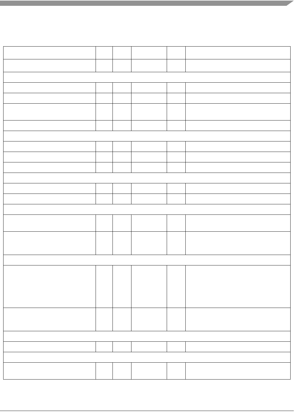
Table 2-1. 1322x-LPB Specifications
Parameter Units Notes/Conditions
MIN TYP MAX
General
Size (Enclosure: X, Y, Z) 74x56x37 mm
Size (PCB: X, Y) 65x45 mm
Layer build (PCB) 0.8 /
0.032 mm /
in 2-Layer
Dielectric material (PCB) FR4
Power
Voltage supply (DC) 4.4 5 12 V
Voltage supply (Batteries) 2.0 3 3.6 V
Current consumption 55 mA
Temperature
Operating temperature -30 +25 +85 °C
Storage temperature -30 +25 +85 °C
RF
Frequency range 2405 2480 MHz All 16 channels in the 2450 MHz band, 5
MHz spacing
Range (outdoor / line of sight) 300 Meter <1% PER for 20-byte packets (point-to-point
in communications with 1322X Sensor
Reference Board)
RF Transmitter
802.15.4 Output power -30 0 +4 dBm Over range of Pout from IC control in 2 dB
steps.
Note: On channel 26, output power should
not exceed -5.5 dBm (Power setting
0x0E) to meet FCC part 15
requirements.
Harmonics
2nd harmonics
3rd harmonics -38
-35
dBm
dBm
Harmonics are compliant to ETSI and FCC
regulatory approval standards
RF Receiver
Sensitivity -95 dBm <1% PER for 20-byte packets
Regulatory Approval
FCC Product complies accordingly to the FCC
part 15 standard
1322x-LPB Module Overview and Description
1322x-LPB Reference Manual, Rev. 1.1
2-4 Freescale Semiconductor
CE (ETSI) Product complies accordingly to the EN 300
328 V1.7.1 (2006-10) standard
CE (EMC) Product complies accordingly to the EN 301
489-1 V1.6.1 (2005-09) and EN 301 489-17
V1.2.1 (2002-08) standards
Safety
UL Product complies accordingly to the IEC
60950-1 and EN 60950-1, First Edition
standards
Environment
RoHS Product complies with the EU Directive
2002/95/EC of 27 January 2003
WEEE Product complies with the EU Directive
2002/95/EC of 27 January 2003
Table 2-1. 1322x-LPB Specifications (continued)
Parameter Units Notes/Conditions
1322x-LPB Reference Manual, Rev. 1.1
Freescale Semiconductor 3-1
Chapter 3
System Overview and Functional Block Descriptions
This section provides an overview of the 1322x-LPB and its block diagram.
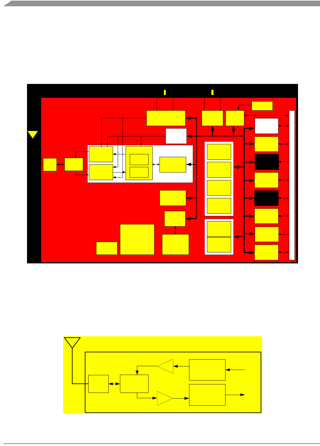
3.1 System Block Diagram
The following is the 1322x-LPB system level block diagram.
Figure 3-1. 1322x-LPB Block Diagram
3.2 Design Overview
The heart of the 1322x-LPB is Freescale’s MC1322x 99-pin LGA Platform-in-Package (PiP) solution that
can be used for wireless applications ranging from simple proprietary point-to-point connectivity to
complete ZigBee mesh networking. The main attributes of the 1322x-LPB module are:
• Small footprint with a 2-layer PCB and F-antenna
• Support for very low power operation
• Support for Lithium coin cell operation
• Support for optional buck converter
• Support for 32.768 KHz crystal oscillator
• Support for non-standard reference oscillator crystal (13-26 MHz and requires use of PLL filter)
MC13224V/225V
Advanced ZigBee™- Compliant PiP
6-Pin
UART
HDR
UART1
JTAG Debug
PCB F-Antenna
24 MHz 32.768
KHz
12-Pin
GPIO
HDR
PLL
Filter
GPIO
2 Pushbuttons
2 LEDs
Power
Manage-
ment
DC Adaptor
2xAAA Battery
Lithium Coin Cell
VCC
SW_VCC
KBI
System Overview and Functional Block Descriptions
1322x-LPB Reference Manual, Rev. 1.1
3-2 Freescale Semiconductor
The MC1322x MCU resources offer superior processing power for ZigBee and IEEE 802.15.4
applications. A full 32-bit ARM7TDMI-S core operates up to 26 MHz. A 128 Kbyte FLASH memory is
mirrored into a 96 Kbyte RAM for upper stack and applications software. In addition, an 80 Kbyte ROM
is available for boot software, peripheral device drivers, standardized IEEE 802.15.4 MAC and
communications stack software. A full set of peripherals and Direct Memory Access (DMA) capability for
transceiver packet data complement the processor core.
Figure 3-2. MC1322x Block Diagram
The RF radio interface provides for low cost and high density as shown in Figure 3-3. An onboard balun
along with a TX/RX switch allows direct connection to a single-ended 50-Ω antenna. The integrated PA
provides programmable output power typically from -30 dBm to +4 dBm, and the RX LNA provides -95
dBm sensitivity. This solution also has onboard bypass capacitors and crystal load capacitors for the
smallest footprint in the industry. All components are integrated into the package except the crystal and
antenna.
Figure 3-3. MC1322x RF Interface
TIMER
MODULE
(TMR)
(4 Tmr Blocks)
UART
MODULE
(UART0)
UART
MODULE
(UART1)
SYNC SERIAL
INTERFACE
(SSI/i2S)
KEYBOARD
INTERFACE
(KBI)
INTER-IC BUS
MODULE
(I2C)
SERIAL
PERIPHERAL
INTERFACE
(SPI)
DUAL
12-BIT
ADC
MODULE
GPIO and IO
CONTROL
UP TO 64 IO PINS
ARM7
TDMI-S
32-BIT
CPU
BUS
INTERFACE
& MEMORY
ARBITRATOR
ARM
INTERRUPT
CONTROLLER
(AITC)
JTAG/
Nexus
DEBUG
ADVANCED
SECURITY
MODULE
(ASM)
CLOCK &
RESET
MODULE
(CRM)
RADIO
INTERFACE
MODULE
(RIF)
96KBYTE
SRAM
(24K WORDS x
32 BITS)
80KBYTE
ROM
(20KWORDS x
32 BITS)
RF
OSCILLATOR
&
CLOCK GENERATION
SPI
FLASH
MODULE
(SPIF)
802.15.4
MAC
ACCELERATOR
(MACA)
DIGITAL
MODEM
TX
MODEM
RX
MODEM
128KBYTE
NON-VOLATILE
MEMORY
(SERIAL
FLASH)
ANALOG
TRANSMITTER
ANALOG
RECEIVER
RF
TX/RX
SWITCH
IEEE 802.15.4 TRANSCEIVER
BALUN
ANALOG
POWER
MANAGEMENT
&
VOLTAGE
REGULATION
MC13225
Platform-in-Package (PiP)
IEEE 802.15.4/ZIGBEE SOLUTION
Buck
Regulator
24 MHz (typ) 32.768 KHz (optional)
BATTERY
DETECT
ANALOG
TRANSMITTER
ANALOG
RECEIVER
RF
TX/RX
SWITCH
BALUN
LNA
PA
System Overview and Functional Block Descriptions
1322x-LPB Reference Manual, Rev. 1.1
Freescale Semiconductor 3-3
3.2.1 1322x-LPB Form Factor
The MC1322x allows for very small footprint applications. The 1322x-LPB circuit board illustrates a
small footprint for the MC1322x/RF area and use of a 2 metal layer design. This board can be used as a
template for a 2-layer PCB design (design files are available), or additional reference designs are available
through the Freescale web site.
Freescale provides a one-stop-shop approach to guide customers with their wireless solutions to help
minimize product time-to-market. One important recommendation is to follow the layout application
guide as described in the Freescale IEEE 802.15.4 / ZigBee Package and Hardware Layout
Considerations Reference Manual (ZHDCRM). This manual describes Printed Circuit Board (PCB)
footprint guidelines for the MC1322x LGA 71 package. Included are layouts of the component copper
layer, solder mask, and solder paste stencil.
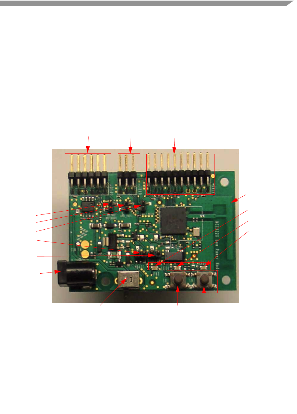
Figure 3-4. 1322x-LPB PCB Top View
Figure 3-4 shows the 1322x-LPB PCB top view. Refer to this figure in the following sections.
DC
JTAG (J1)
UART (J3)
GPIO (J2)
Power
Connect
Power Switch SW1 SW2
Power LED
LED 1
LED 2
F-Antenna
J18
J20
J19
J16
J17
System Overview and Functional Block Descriptions
1322x-LPB Reference Manual, Rev. 1.1
3-4 Freescale Semiconductor
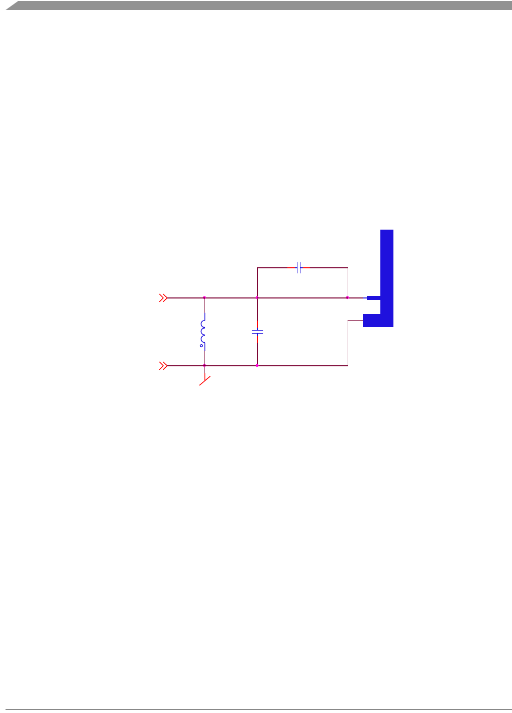
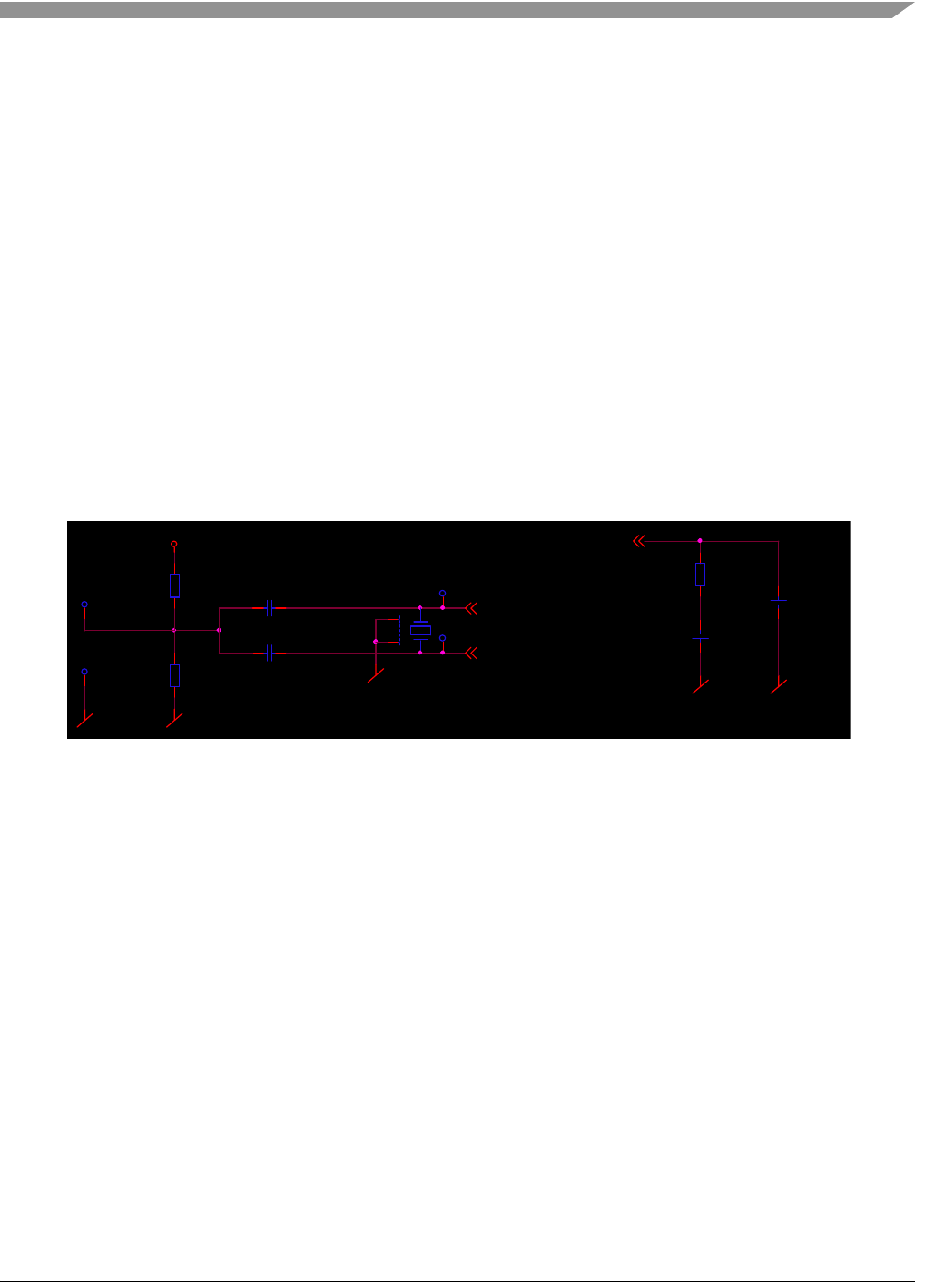
3.3 RF 2.4 GHz ISM Band radio design
The MC1322x transceiver includes a low noise amplifier, 1mW nominal output power, PA with internal
voltage controlled oscillator (VCO), integrated transmit/receive switch, on-board power supply regulation,
and full spread-spectrum encoding and decoding. The 1322x-LPB requires only a minimum amount of
external components and a chip-antenna for a complete solution. Figure 3-5 shows the RF network
external to the MC1322x.
• Typical nominal output power is 0 dBm, with +4 dBm max
• Typical sensitivity is -95 dBm.
• Frequency range is 2405 to 2480 MHz
• Typical range (outdoors, line of sight) is 300 meters
• Uses a minimum number of RF components
Figure 3-5. 1322x-LPB RF Network.
3.4 Power Sources
To allow maximum versatility, the 1322x-LPB can be powered via a DC source (nominally 5 VDC) or a
variety of battery sources.
• An “OFF/ON” slide switch (SW5) is provided that disconnects all supplies, no matter which is
active.
• A green “PWR” LED (D5) is provides as a Power-On indicator.
• All sources are isolated via diodes.
3.4.1 External DC Source
The DC source is typically an AC-DC converter
• The DC source can be from 4.4 to 12 VDC
• When connected, it automatically shuts down the battery supply.
• The DC source is regulated to 3.3 V; however, the raw battery pack voltage directly supplies the
circuitry
ANT1
F_Antenna
L1
3.9nH
Not Mounted
C3
1pF
Not Mounted
RF
C1
10pF
Not Mounted
RF_RX_TX
RF_GND

System Overview and Functional Block Descriptions
1322x-LPB Reference Manual, Rev. 1.1
Freescale Semiconductor 3-5
3.4.2 Battery Sources
The battery source can be either a AAA battery pack (2 cells) or an optional Lithium coin cell:
• AAA source - as supplied, the 1322x-LPB has a 2-cell AAA battery holder mounted. The typical
usable voltage range for 2 AAA cells is ~3.1V down to 2.2 - 2.0V. Note that a Schottky diode and
a switch MOSFET are in series with the battery pack, and these will impact the lowest usable
voltage for the battery pack.
• Lithium coin cell source - in some very low duty cycle applications where the system mostly
“sleeps” in low power, the use of a Lithium coin cell can be considered. To assist in this design, the
1322x-LPB supports mounting a socket for a coin cell
— The AAA battery holder must first be removed.
— Mount one of two sockets for a Lithium coin cell
– Renata #SMTU2477N-1 - SMD holder for CR2477N cell (950 mAh)
– Renata #SMTU2450N-1 - SMD holder for CR2450N cell (540 mAh)
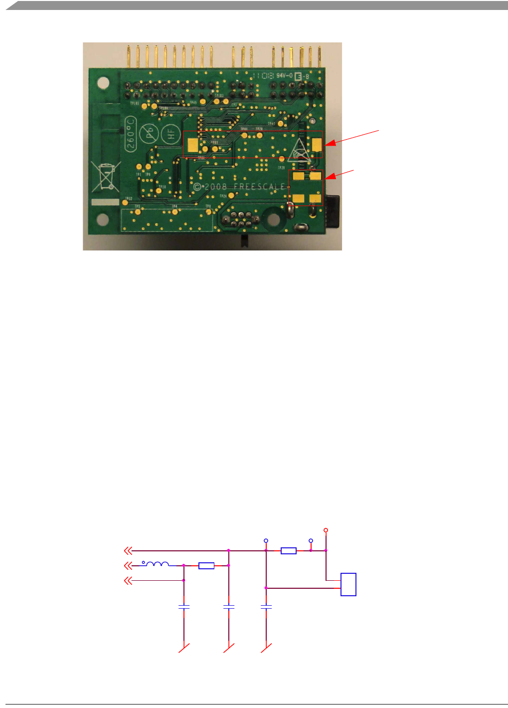
— The bottom view of the 1322x-LPB is shown in Figure 3-6.
– The mounting pads for the socket are noted (both sockets use the same pads). Be sure to
observe proper polarity.
– The mounting pads for two 100µF tantalum capacitors (C59 & C60) are also provided.
NOTE
Designing with Manganese Dioxide Lithium Coin Cell technology can be
very challenging. It is recommended to consider the following:
• Source impedance is high, typically about 25 ohms. Consider the
fluctuation in source voltage under heavy current load (~20 mA or
more).
• The addition of heavy bulk capacitance (such as C59 & C60) on VCC
can help minimize voltage drop under heavy current.
• High current duty cycle is critical; every effort must be made to
minimize high current activity (primarily TX and RX).
• When developing a coin cell application, it is highly recommended to
use the external DC source for all code development and early testing.
Life of coin cells can be very short with continual and/or heavy load.
System Overview and Functional Block Descriptions
1322x-LPB Reference Manual, Rev. 1.1
3-6 Freescale Semiconductor
Figure 3-6. 1322x-LPB PCB Bottom View
3.4.3 Optional Use of MC1322x Buck Regulator
The MC1322x is typically used in a single source, unregulated VCC configuration (VBATT connected in
parallel with LREG_BK_FB), and the 1322x-LPB is supplied in this connection. However, the MC1322x
also has an optional buck switched regulator, and the 1322x-LPB supports use of the buck function.
Figure 3-7 shows the VCC connection at the MC1322x device. The PCB is supplied with the 0-ohm R66
component mounted, which is the simple non-regulated configuration. To allow use of the buck regulator:
• Remove R66
• Mount L2; an SMD power 100uH inductor, from manufacturer TDK # SLF6028T-101MR42-PF
(see Chapter 4, “Schematic, Board Layout, and Bill of Materials”).
• Mount C52; a 100 µF ceramic capacitor.
NOTE
Use of the buck converter requires proper initialization, control and support
through the application software. Refer to the MC1322x Reference Manual.
Figure 3-7. MC1322x Main Power Connection
C59 and C60 Pads
Socket Pads
1
1
2
2
J16
TSM-102-01-L-SV
TP44
C52
10uF
Not Mounted
C8
100pF
TP45
Current Measurement
L2
100uH
Not Mounted
R65
0R
Not Mounted
VCC
R66
0R
C10
1uF
Not Mounted
VBATT
COIL_BK
LREG_BK_FB
System Overview and Functional Block Descriptions
1322x-LPB Reference Manual, Rev. 1.1
Freescale Semiconductor 3-7
3.5 Clock Sources
The 1322x-LPB supports two primary clock sources for the MC1322x.
3.5.1 Reference Oscillator (24 MHz nominal)
The reference oscillator is the primary source for all internal MC1322x clocks. Figure 3-8 shows the LPB
circuitry related to the reference oscillator. The default frequency for the reference oscillator is 24 MHz
and the mounted crystal X1 is a 24 MHz device that meets MC1322x specifications. There are two
additional options for the module:
• X1 can be replaced by a 13-26 MHz crystal - It must meet MC1322x specifications. In addition,
the onboard PLL must be used in this case. The PCB provides for the PLL filter components, but
these are not populated. To use a non-standard crystal, the PLL filter components of R5, C4, and
C5 must be populated. Also, software must enable use of the PLL for the internal modem clock.
• An external clock source can be supplied as the reference source - This is typically 24 MHz. The
frequency must be accurate to +/-40ppm. The external clock source can supplied via test point
TP86 and C57 (10 pF) must also be installed.
Figure 3-8. Reference Oscillator Related Circuitry
C58
10pF
Not Mounted
R73
1K
Not Mounted
VCC
R72
1K
Not Mounted
C57
10pF
Not Mounted
TP1
TP9
X1
24.00MHz
External
Clock
Source
TP87
TP86
R5
240R
Not Mounted
C5
180nF
Not Mounted
C4
27nF
Not Mounted
RF_PLL_FLT
XTAL_24_OUT
XTAL_24_IN
PLL External Filter
System Overview and Functional Block Descriptions
1322x-LPB Reference Manual, Rev. 1.1
3-8 Freescale Semiconductor
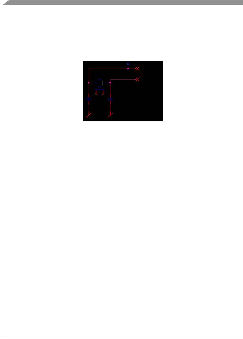
3.5.2 32.768 kHz Crystal Oscillator
Provision is also made for the secondary 32.768 kHz oscillator crystal X2. This oscillator can be used on
the MC1322x for a low power accurate RTC timebase and wake-up state machine. The module comes with
this crystal and its load capacitors C7 and C12 mounted. Although use of the oscillator is optional, the
module is provided ready for use. See Figure 3-9.
Figure 3-9. 32.768 KHz Oscillator Related Circuitry
3.6 FLASH Memory Recovery Jumpers and Erase
The MC1322x has an onboard serial FLASH that stores the memory image that gets loaded into RAM at
boot. If it becomes necessary to change or update the image in FLASH, there are two possible means of
doing so:
• JTAG Debug Port - Using the JTAG debug port and the ARM debug tools, the FLASH image can
be changed.
• Load new FLASH image via UART1 port -
NOTE
The 1322x-LPB provides a header for UART1 that is NOT buffered for
RS232 operation. If users must employ UART1 with the Freescale Test Tool
running on a PC, they must provide an appropriate RS232 interface board to
connect to a PC serial COM port.
— The Freescale BeeKit IDE suite download provides a software tool called “Test Tool”. This
application runs on a PC and can be used with a client running on the MC1322x to test the
platform.
— Test Tool also has the capability to load a new image into the FLASH.
NOTE
The FLASH must be cleared before loading a new image.
The 1322x-LPB has two jumper sites designated as J19 and J20 (see Figure 3-4) that must be used to erase
the FLASH:
1. Short Jumper J19 Pin 1 to Pin 2 with a shorting bar, as well as, short Jumper J20 Pin 1 to Pin 2 with
a second shorting bar
2. Turn on power, push the reset button, and wait a few seconds.
C7
22pF
C12
22pF
X2
32.768kHz
TP10
XTAL_ 32 _OU T
XTAL_ 32 _I N
System Overview and Functional Block Descriptions
1322x-LPB Reference Manual, Rev. 1.1
Freescale Semiconductor 3-9
3. Turn off power and remove the jumper shorts as required.
4. The board is now ready for boot operation.
After the FLASH is erased, the module can be loaded with a new image through the UART1 port using
Test Tool. Refer to the Test Tool User’s Guide as supplied with Test Tool in the BeeKit download.
Figure 3-10. FLASH Erase Headers
3.7 Low Power Operation
The 1322x-LPB intended to develop low power operation and applications code. It has been designed to
allow low current measurement and support MC1322x low power application needs.
NOTE
It is strongly suggested that the user review the low power considerations
described in the MC13224/225 Reference Manual.
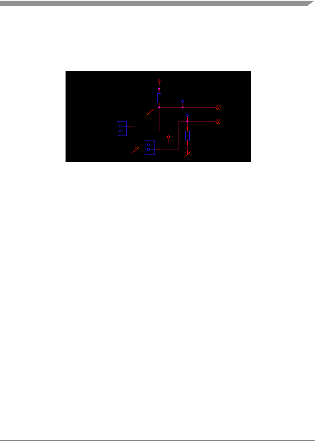
3.7.1 Switched VCC for Peripheral Functions
The MC1322x by default does not retain power to its GPIO pads while in low power mode (KBI signals
are the exception and do retain power). As a result, GPIO pads should not be driven high while the device
is in low power or extraneous current exist. The 1322x-LPB provides a switched VCC for devices
connected to the MC1322x while low power mode so that these devices can be disabled when appropriate.
Figure 3-11 shows the switched VCC circuit.
• A P-channel MOSFET is used as a switch to turn SW_VCC ON or OFF as required.
• The MOSFET gate is driven by signal KBI_3 which is always powered and defaults to an output
in the high state when in low power. This condition turns off SW_VCC in low power mode.
NOTE
The user must program/control GPIO25 under run (operational) mode. The
KBI pins are controlled by the CRM in low power mode; they revert to their
GPIO control during normal run mode. As a result, GPIO25 must be
programmed as an output and controlled to enable SW_VCC as appropriate
for use, or alternatively, GPIO can be programmed as the KBI function
under normal operation.
1-2 ADC2_VREFH -> "0"
3-4 ADC2_VREFL -> "1"
Recovery M ode
VCC R104
10K
C2
100nF
TP103
R103
10K
SW_VCC
TP3
1
2
J19
HDR_1X2 1
2
J20
HDR_1X2
ADC2_VREH
ADC2_VREFL
System Overview and Functional Block Descriptions
1322x-LPB Reference Manual, Rev. 1.1
3-10 Freescale Semiconductor
• SW_VCC is provided on the J2 GPIO Pin Header
• SW_VCC also powers U17 the voltage reference for ADC operation.
Figure 3-11. Switched VCC for Peripheral Devices
3.7.2 Measuring Current
The 1322x-LPB provides three primary points for current measurement:
• Total current to the board - reference Figure 3-11. R68 can be removed and current can be
measured between TP29 and TP47.
• Total current to the MC13224/225 - reference Figure 3-7. R65 can be removed and current can be
measured through jumper J16.
• ADC voltage reference current - reference Figure 3-12. Voltage reference U17 is enabled via J18;
current can be measured through this jumper.
3.7.3 Other Low Power Considerations
When designing low power operation, consider:
• Indicator LEDs D1 and D2 are connected to ground not VCC, so as to not put GPIO high during
low lower mode.
• The GPIO connector (J2) provides access and connectivity to the MC13224/225
— SW_VCC is provided.
— No peripheral device should pull a GPIO high during low power mode
— Signal SWITCH1 is connected to KBI_4 and can be used as a wake-up interrupt to the
MC13224/225. See the CRM chapter of the MC13224/225 Reference Manual.
— Signal SWITCH2 is connected to KBI_0 and can be used as a wake-up signal from the
MC13224/225 to an external device. See the CRM chapter of the MC13224/225 Reference
Manual.
• The UART1 connector (J3) provides direct access to the MC13224/225 GPIO. If low power mode
is enabled and UART1 is connected to an external device, extraneous high leakage current can
occur if any of the UART1 signals is driven high.
KBI_3
SW_VCC
TP32
R68
0R
TP47 VCCTP29
C56
4.7uF
Q2
FDV302
MAIN SUPPLY
System Overview and Functional Block Descriptions
1322x-LPB Reference Manual, Rev. 1.1
Freescale Semiconductor 3-11
3.8 User Interfaces
This section provides a summary of the user interfaces.
3.8.1 LEDs, Switches, and Reset
For application interface the 1322x-LPB provides:
• Two red LEDs (D1 and D2)are driven by the MCU and controlled by the software application.
• Two pushbuttons (SW1 and SW2) are connected to the MCU GPIO for software application. Only
SW1 has interrupt generation capability, and can be used as an input for low power wake-up.
• Jumper J17 provides a hardware reset capability. Shorting Pin 1 to Pin 2 causes the hardware reset
input to be held low and resets the MC13224/225.
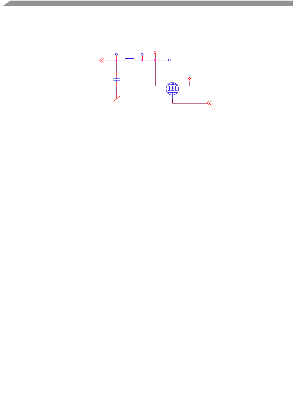
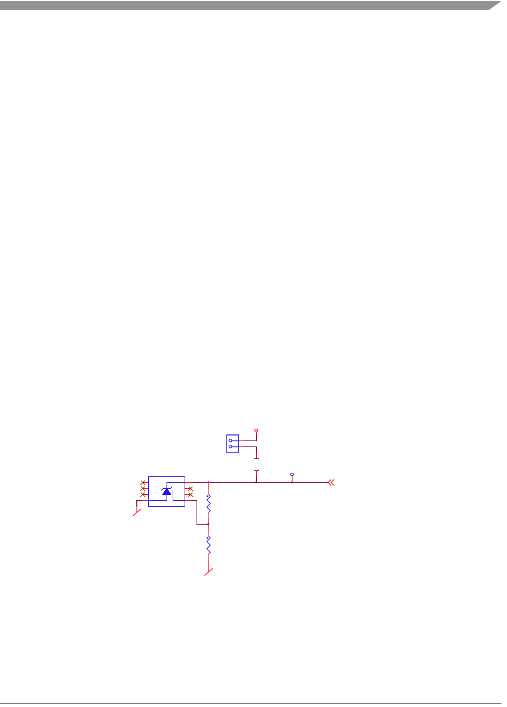
3.8.2 ADC Voltage References
When using the ADC input channels ADC2 and ADC3 (through J2), consider;
• The ADC high voltage reference ADC2_VREFH is tied to SW_VCC through a resistor. This
reference is not absolute and will move as VCC decreases with battery operation.
• A fixed voltage reference for ADC1_VREFH is provided (see Figure 3-12).
— The fixed voltage is 1.5 VDC.
— The LM285M (U17) is programmed via R120 and R121 to provide a constant reference
— The reference can be enabled via jumper J18. This number can also be used to measure current
to the reference circuit.
— This reference is useful for battery operation where a known, fixed high reference voltage for
the ADC is required.
Figure 3-12. ADC Voltage 1.5 VDC Voltage Reference
R1
10K
SW_VCC
1
2
J18
HDR_1X2
R120
120K
1%
R121
24.9K
1%
TP106
1.5V
1
1
2
2
3
3
4
455
66
77
88
U17
LM285M
ADC1_VREFH
System Overview and Functional Block Descriptions
1322x-LPB Reference Manual, Rev. 1.1
3-12 Freescale Semiconductor
3.8.3 ARM JTAG Debug Interface Connector
The MC1322x supports connection to a subset of the defined ARM JTAG connector. The JTAG interface
is a standard 2.54mm/0.1inch spacing, 20-pin debug interface (J1). The 20-pin connector is clearly
separated from the GPIO and UART pin headers and located at the rear side of the module. The 20-pin
connector is designated “JTAG” on the silk-screen and has Pin 1 designated for correct plug-in of the
development cable.
Table 3-1 shows the device pins that are connected to the associated JTAG header pinouts.
3.8.4 GPIO Connector
The GPIO connector (J2) is a standard 2.54mm/0.1inch spacing, 12-pin header. The connector provides
access to MCU GPIO, two timer GPIOs, two ADC inputs, UART2 port, and the I2C port. Power is also
provided on the connector.
• SW_VCC is the main supply voltage. Current draw should be limited to 50 mA.
• Signals SWITCH1 and SWITCH2 are in parallel with onboard switches SW1 and SW2.
• KBI signals are provided through SWITCH1 and SWITCH2 for low power control and interface
Table 3-1. ARM JTAG 20-Pin Connector Assignments (J1)
Name1
1NC means No Connect.
Pin # Pin # Name
VCC 1 2 VCC
NC2
2MC1322x does not support separate JTAG reset TRST.
34GND
TDI 5 6 GND
TMS 7 8 GND
TCK 9 10 GND
RTCK 11 12 GND
TDO 13 14 GND
RESET3
3VCC through a 100k-ohm pullup.
15 16 GND
NC 17 18 GND
NC 19 20 GND
Table 3-2. GPIO Connector J2 Pinouts
Pin
Number Name Function Notes
1 UART2_RX UART2 RX data input / GPIO19 UART2 receive data input.
2 UART2_TX UART2 TX data output / GPIO18 UART2 transmit data output.
3I2C_SDA I
2C Bus data / GPIO13 I2C bus signal SDA. Pull-up to SW_VCC
available
System Overview and Functional Block Descriptions
1322x-LPB Reference Manual, Rev. 1.1
Freescale Semiconductor 3-13
3.8.5 UART Connector
The UART connector (J3) is a standard 2.54mm/0.1inch spacing, 6-pin header. The connector provides
access to the unbuffered UART1 signals. Power is also provided on the connector.
• VCC is the main board supply voltage. Current draw should be limited to 50 mA.
• If low power mode is enabled on the module, all signals on J3 must be not be driven high.
• Signals are unbuffered for RS232; an adaptor board is needed to talk to a PC serial COM port
4I2C_SCL I
2C Bus clock / GPIO12 I2C bus signal SCL. Pull-up to SW_VCC
available
5 TMR3 Timer 3 IO signal / GPIO11 Pin can be used as Counter 3 output or counter
input clock.
6 TMR1 Timer 1 IO signal / GPIO9 Pin can be used as Counter 1 output or counter
input clock.
7 ADC3 ADC analog input Channel 3/ GPIO33 ADC sample channel can be used by either
ADC1 or ADC2.
8 ADC2 ADC analog input Channel 2/ GPIO32 ADC sample channel can be used by either
ADC1 or ADC2.
9 SWITCH1 KBI_4 input/ GPIO26 Asynchronous interrupt input can be used as
wake-up signal.
10 SWITCH2 KBI_0_HST_WK output/ GPIO22 Can be used as a wake-up indicator output to
external device.
11 GND System ground
12 SW_VCC Switched voltage supply
Table 3-3. UART Connector J3 Pinouts
Pin
Number Name Function Notes
1 UART1_RX UART1 RX data input / GPIO19 UART2 receive data input.
2 UART1_TX UART2 TX data output / GPIO18 UART2 transmit data output.
3 UART1_CTS UART1 Clear to Send output / GPIO16 UART1 CTS control output.
4 UART1_RTS UART1 Request to Send input / GPIO17 UART1 RTS control input.
5 GND System ground
6 VCC Main voltage supply
Table 3-2. GPIO Connector J2 Pinouts (continued)
System Overview and Functional Block Descriptions
1322x-LPB Reference Manual, Rev. 1.1
3-14 Freescale Semiconductor
3.8.6 Jumper Selection
Table 3-4 lists all the possible jumper selections for the 1322x-LPB. The jumpers available on the board
are:
• J16 - used to measure MC1322x current
• J17 - used to reset MC1322x
• J18 - used to enable 1.5V reference
• J19, J20 - used to recover/clear FLASH. See Table 3-4.
Table 3-4. LPB Jumper Selection
Pin Header Pin Number
Connection Description Default Setting
J16 1-2 Connect to ammeter to measure MC1322x current. R65
should be removed Not mounted. Can
be mounted for
operation w/o R65
J17 1-2 Connect to reset MC1322x Not mounted
J18 1-2 Connect to enable 1.5V reference Not mounted
J19, J20 1-2, 1-2 Connect both to recover/clear FLASH. See Section 3.6,
“FLASH Memory Recovery Jumpers and Erase” Not mounted
1322x-LPB Reference Manual, Rev. 1.1
Freescale Semiconductor 4-1
Chapter 4
Schematic, Board Layout, and Bill of Materials
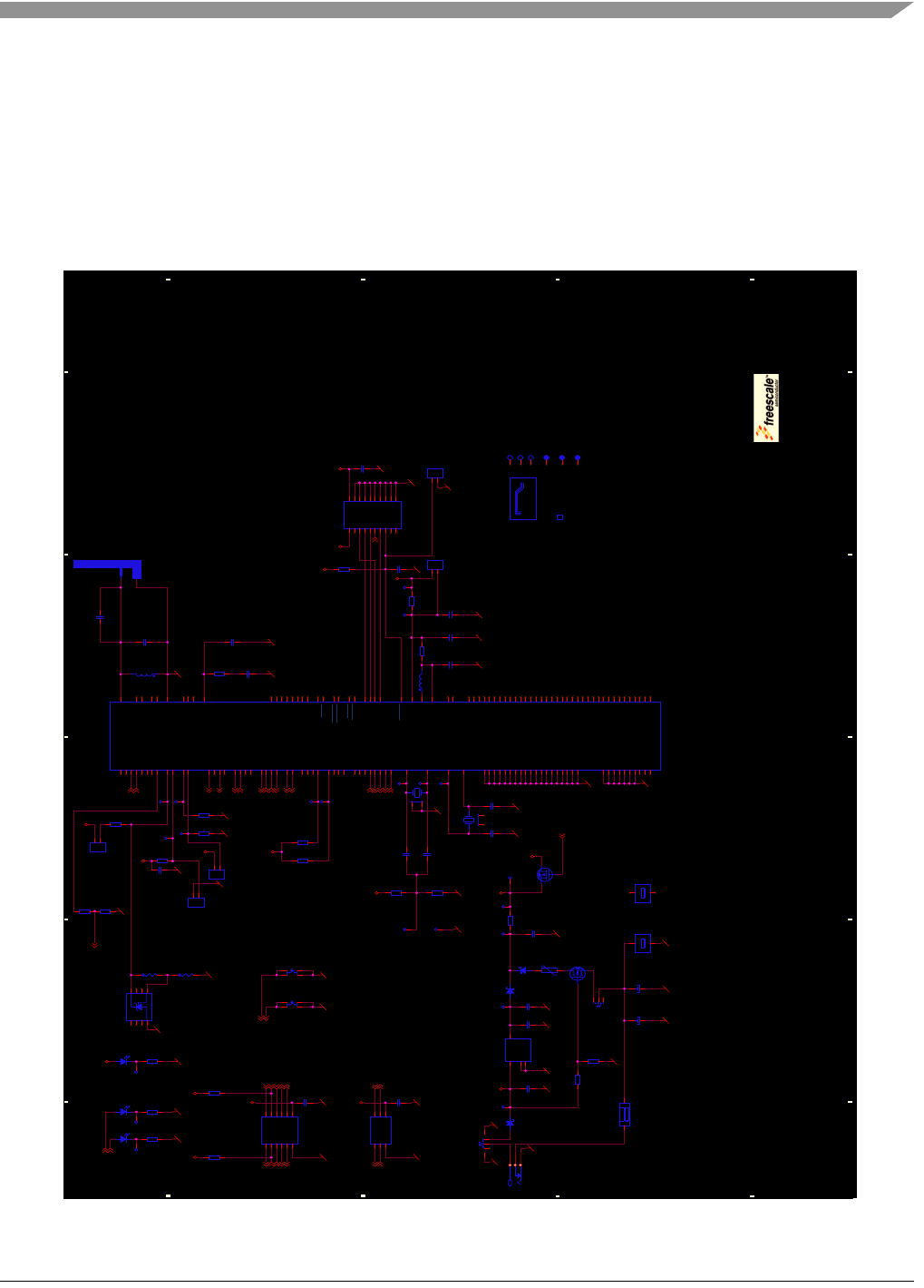
Figure 4-1. 1322x-LPB Schematic
5
5
4
4
3
3
2
2
1
1
D D
C C
B B
A A
VCC
VCC VCC
VCC
V_MAIN VCC
VCC
SW_VCC
VCC
VCC
VCC
SW_VCC
SW_VCC
SW_VCC
SW_VCC
SW_VCC SW_VCC
LED1
LED2
SWITCH2
SWITCH1
LED1
LED2
SWITCH2
SWITCH1
UART1_TX
UART1_CTS
UART1_RX
UART1_RTS
RTCK
RTCK
UART2_RX
I2C_SCL
ADC3
ADC2
UART2_TX
UART2_RX
I2C_SDA
I2C_SCL
I2C_SDA
TMR1
TMR1
UART2_TX
UART1_TXUART1_RX
TMR3
TMR3
SWITCH1 SWITCH2
UART1_RTSUART1_CTS
ADC2ADC3
KBI_3
KBI_3
Drawing Title:
Size Document Number Rev
Date: Sheet of
Page Title:
ICAP Classification: FCP: FIUO: PUBI:
SOURCE: SCH-23453 PDF: SPF-23453 B
1322X-LPB
C
Tuesday, April 08, 2008
Main Schematic
33
_X_ ---
---
Drawing Title:
Size Document Number Rev
Date: Sheet of
Page Title:
ICAP Classification: FCP: FIUO: PUBI:
SOURCE: SCH-23453 PDF: SPF-23453 B
1322X-LPB
C
Tuesday, April 08, 2008
Main Schematic
33
_X_ ---
---
Drawing Title:
Size Document Number Rev
Date: Sheet of
Page Title:
ICAP Classification: FCP: FIUO: PUBI:
SOURCE: SCH-23453 PDF: SPF-23453 B
1322X-LPB
C
Tuesday, April 08, 2008
Main Schematic
33
_X_ ---
---
GPIO
Pin Header
Push
Buttons
LEDs
RF
JTAG Debug
DBGRQ
DBGACK
nTRST
JTAG RTCK
Enable
Power ON
JTAG RTCK
Disable
External
Clock
Source
Power Management Power Measurement
2xAAA Cells
CR2477N
UART
Pin Header
J19 VREFH -> "0"
J20 VREFL -> "1"
Recovery Mode
CR2450N
Reset
1.5V
Current Measurement
C8
100pF
C8
100pF
X2
32.768kHz
X2
32.768kHz
R11
220R
R11
220R
R73
1K
Not Mounted
R73
1K
Not Mounted
TP3TP3
TP10TP10
J4
DJ-005
J4
DJ-005
1
3
2
C54
100nF
C54
100nF
R105
0R
R105
0R
D6
MBR0520LT1
D6
MBR0520LT1
R120
120K
1%
R120
120K
1%
J18
TSM-102-01-L-SV
J18
TSM-102-01-L-SV
11
22
C58
10pF
Not Mounted
C58
10pF
Not Mounted
R6
390R
R6
390R
TP103TP103
REF3
Ref
REF3
Ref
1
1
R104
10K
R104
10K
U17
LM285M
U17
LM285M
1
1
2
2
3
3
4
455
66
77
88
R121
24.9K
1%
R121
24.9K
1%
J19
TSM-102-01-L-SV
J19
TSM-102-01-L-SV
11
22
R70
100K
R70
100K
C52
10uF
Not Mounted
C52
10uF
Not Mounted
R106
4.7K
Not Mounted
R106
4.7K
Not Mounted
TP29TP29
C11
1nF
C11
1nF
J20
TSM-102-01-L-SV
J20
TSM-102-01-L-SV
11
22
R5
240R
Not Mounted
R5
240R
Not Mounted
R69
10K
R69
10K
MH2MH2
1
C4
27nF
Not Mounted
C4
27nF
Not Mounted
TP45TP45
TP32TP32
TP85TP85
+
C59
100uF
Not Mounted
+
C59
100uF
Not Mounted
R68
0R
R68
0R
R3
0R
R3
0R
SW2
DTSM63N
SWITCH2
SW2
DTSM63N
SWITCH2
3
12
4
TP8TP8
REF1
Ref
REF1
Ref
1
1
X1
24.00MHz
X1
24.00MHz
R1
10K
R1
10K
C3
1pF
Not Mounted
C3
1pF
Not Mounted
BC3
SMTU2450N-1
Not Mounted
BC3
SMTU2450N-1
Not Mounted
+
1
-
2
ZZ1
Label 1322X-LPB
ZZ1
Label 1322X-LPB
L1
3.9nH
Not Mounted
L1
3.9nH
Not Mounted
C2
100nF
C2
100nF
TP1TP1
TP47TP47
C53
1uF
C53
1uF
D7
MBR0520LT1
D7
MBR0520LT1
C12
22pF
C12
22pF
C57
10pF
Not Mounted
C57
10pF
Not Mounted
TP26TP26
+
C60
100uF
Not Mounted
+
C60
100uF
Not Mounted
R4
0R
Not Mounted
R4
0R
Not Mounted
U1
MC13225
U1
MC13225
UART2_RTS
13
EVTI_B 132
MCKO/IO50 131
MSEO0_B 114
EVTO_B 123
RDY_B 122
MSEO1_B 113
VBATT 45
LREG_BK_FB 44
COIL_BK 43
ADC2_VREFL
61 ADC1_VREFL
62
ADC1_VREFH
63
ADC2_VREFH
64
ADC0
1
ADC1
2
ADC2
3
ADC3
4
ADC4
5
ADC5
6
ADC6
7
ADC7_RTCK
8
MDO00 103
MDO01 102
MDO02 112
MDO03 111
MDO04 121
MDO05 120
MDO06 130
MDO07 129
TDI 10
RF_GND 58
TDO 9
UART2_CTS
14
UART2_RX
15
TCK 11
TMS 12
RESETB 51
VREG_ANA 55
XTAL_24_OUT
49
RF_PLL_FLT 46
XTAL_24_IN
50
KBI_0_HST_WK
42
XTAL_32_IN
47
ANT_1 56
XTAL_32_OUT
48
RF_RX_TX 60
ANT_2 57
UART2_TX
16
RX_ON 59
PA_POS 54
PA_NEG 53
TX_ON 52
UART1_RTS
17
UART1_CTS
18
UART1_RX
19 UART1_TX
20
I2C_SDA
21
I2C_SCL
22
TMR3
23
TMR2
24
TMR1
25
TMR0
26
SPI_SCK
27
SPI_MOSI
28
SPI_MISO
29
SPI_SS
30
SSI_BITCK
31
SSI_FSYN
32
SSI_RX
33 SSI_TX
34
KBI_1
41 KBI_2
40 KBI_3
39 KBI_4
38 KBI_5
37 KBI_6
36 KBI_7
35
GND_FLAG_1
75
DIG_REG 124
NVM_REG 133
GND_FLAG_2
76
GND_FLAG_3
77
GND_FLAG_4
78
GND_FLAG_5
79
GND_FLAG_6
84
GND_FLAG_7
85
GND_FLAG_8
86
GND_FLAG_9
87
GND_FLAG_10
88
GND_FLAG_11
93
GND_FLAG_12
94
GND_FLAG_13
95
GND_FLAG_14
96
GND_FLAG_15
97
GND_FLAG_16
104
GND_FLAG_17
105
GND_FLAG_18
106
GND_FLAG_19
115
NC1
65
NC2
66
NC3
67
NC4
68
NC5
69
NC6
70
NC7
71
NC8
72
NC9
73
NC10
74
NC11 80
NC12 81
NC13 82
NC14 83
NC15 89
NC16 90
NC17 91
NC18 92
NC19 98
NC20 99
NC21 100
NC22 101
NC23 107
NC24 108
NC25 109
NC26 110
NC27 116
NC28 117
NC29 118
NC30 119
NC31 125
NC32 126
NC33 127
NC34 128
NC35 134
NC36 135
NC37 136
NC38 137
NC39 138
NC40 139
NC41 140
NC42 141
NC43 142
NC44 143
NC45 144
NC46 145
R103
10K
R103
10K
BC1
2468
BC1
2468
+1
-
2
R72
1K
Not Mounted
R72
1K
Not Mounted
PCB1
JDP7051_2
PCB1
JDP7051_2
TP9TP9
BC2
SMTU2477N-1
Not Mounted
BC2
SMTU2477N-1
Not Mounted
+
1
-
2
R12
100K
R12
100K
RT1
500mA
RT1
500mA
TP5TP5
R74
10K
R74
10K
C56
4.7uF
C56
4.7uF
J2
90122-12
J2
90122-12
1
1
3
3
5
5
7
7
9
9
11
11
22
44
66
88
10 10
12 12
C1
10pF
Not MountedC1
10pF
Not Mounted
J16
TSM-102-01-L-SV
J16
TSM-102-01-L-SV
1
1
2
2
C6
100nF
C6
100nF
MH1MH1
1
MH3MH3
1
D2
LHR974
LED2
D2
LHR974
LED2
SW5B
MFP213N-RA
SW5B
MFP213N-RA
4
5
6
C5
180nF
Not Mounted
C5
180nF
Not Mounted
R65
0R
R65
0R
D5
LGR971
POWER
D5
LGR971
POWER
J17
TSM-102-01-L-SV
J17
TSM-102-01-L-SV
1
1
2
2
C55
4.7uF
C55
4.7uF
C10
1uF
Not Mounted
C10
1uF
Not Mounted
R107
4.7K
Not Mounted
R107
4.7K
Not Mounted
C50
100nF
C50
100nF
C51
100nF
C51
100nF
J1
90122-20
J1
90122-20
1
1
3
3
5
5
7
7
9
9
11
11
13
13
15
15
17
17
19
19
22
44
66
88
10 10
12 12
14 14
16 16
18 18
20 20
Q1
ZXM61P02F
Q1
ZXM61P02F
REF2
Ref
REF2
Ref
1
1
TP4TP4
J3
90122-6
J3
90122-6
1
1
3
3
5
5
22
44
66
U2
LT1129CST-3.3
U2
LT1129CST-3.3
Vin
1Vout 3
GND1
2
GND2
4
TP87TP87
L2
100uH
Not Mounted
L2
100uH
Not Mounted
SW1
DTSM63N
SWITCH1
SW1
DTSM63N
SWITCH1
3
12
4
ANT1
F_Antenna
ANT1
F_Antenna
TP28TP28
TP84TP84
C7
22pF
C7
22pF
R71
10K
Not Mounted
R71
10K
Not Mounted
TP44TP44
TP86TP86
R7
390R
R7
390R
Q2
FDV302
Q2
FDV302
SW5A
MFP213N-RA
SW5A
MFP213N-RA
1
2
3
7 8
D1
LHR974
LED1
D1
LHR974
LED1
TP105TP105
R66
0R
R66
0R
TP104TP104
D8
MBR0520LT1
D8
MBR0520LT1

Schematic, Board Layout, and Bill of Materials
1322x-LPB Reference Manual, Rev. 1.1
4-2 Freescale Semiconductor
Figure 4-2. 1322x-LPB PCB Component Location (Top View)
Figure 4-3. 1322x-LPB PCB Test Points (Bottom View)
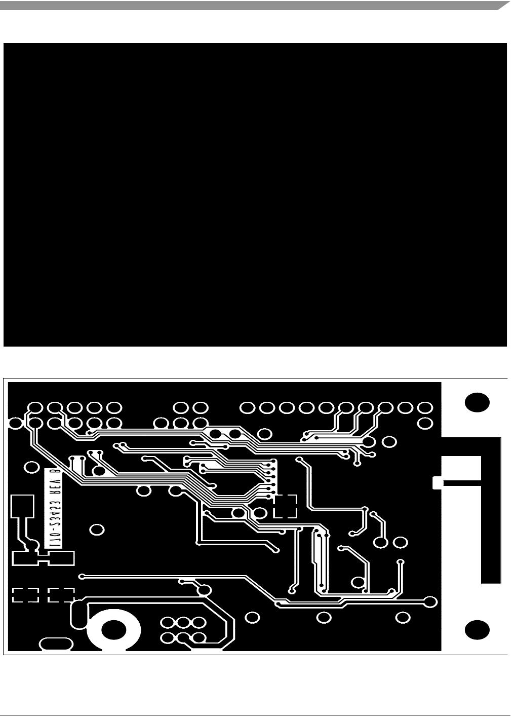
Schematic, Board Layout, and Bill of Materials
1322x-LPB Reference Manual, Rev. 1.1
Freescale Semiconductor 4-3
Figure 4-4. 1322x-LPB PCB Layout (Top View)
Figure 4-5. 1322x-LPB PCB Layout (Bottom View)

Schematic, Board Layout, and Bill of Materials
1322x-LPB Reference Manual, Rev. 1.1
4-4 Freescale Semiconductor
Table 4-1. Bill of Materials
Qty Part
Reference Description Value Voltage Power Tolerance Manufacturer Manufacturer
Part Number
1 ANT1 PCB F ANTENNA F ANTENNA NOT A PART NOT A PART
1 BC1 PCB Battery Holder
2xAAA 2468 Keystone 2468
0 BC2 Surface mount coin
cell holder CR2477N SMTU2477N-1 Reneta SMTU2477N-1
0 BC3 Surface mount coin
cell holder CR2450N SMTU2450N-1 Renata SMTU2450N-1
0 C1,C57,C5
8Ceramic Capacitor
COG 10pF 50V 5% Murata GRM1555C1H1
00JZ01
5 C2,C6,C50
,C51,C54 Ceramic Capacitor
X5R 100nF 10V 10% Murata GRM155R61A1
04KA01D
0 C3 Ceramic Capacitor
COG 1pF 50V 0.25pF Murata GRM1555C1H1
R0CZ01D
0 C4 Ceramic Multilayer
Capacitor X7R 27nF 10V 5% Vishay VJ0402Y273JX
QCW1BC
0 C5 Ceramic Multilayer
Capacitor X7R 180nF 16V 5% Vishay VJ0603Y184JX
JCW1BC
2 C7,C12 Ceramic Capacitor
COG 22pF 50V 5% Murata GRM1555C1H2
20JZ01J
1 C8 Ceramic Capacitor
COG 100pF 50V 5% Murata GRM1555C1H1
01JZ01
0 C10 Ceramic Capacitor
X5R 1uF 6.3V 10% Murata GRM155R60J1
05KE19B
1 C11 Ceramic Capacitor
X7R 1nF 50V 10% Murata GRM155R71H1
02KA01D
0 C52 Ceramic Capacitor for
smoothing X5R 10uF 10V 10% Murata GRM21BR61J1
06KE19L
1 C53 Ceramic Multilayer
Capacitor X7R NoPb 1uF 16V 15% Murata GRM21BR71C
105
2 C55,C56 Ceramic Multilayer
Capacitor X5R 4.7uF 16V 15% Phycomp 2222 781 13672
0 C59,C60 Low ESR Tantal
Capacitor 100uF 16V +/-10% AVX TPSD107K016
R150
2 D1,D2 SMD Red topled LHR974 OSRAM Q62702P5182
1 D5 SMD Green topled LGR971 OSRAM Q65110P5179
3 D6,D7,D8 SMD Power Schottky
Rectifier MBR0520LT1 20V On
Semiconductor MBR0520LT1G

Schematic, Board Layout, and Bill of Materials
1322x-LPB Reference Manual, Rev. 1.1
Freescale Semiconductor 4-5
1 J1 Dual Row Right Angle
pin header 0.38um
gold
90122-20 Molex 90122-0770
1 J2 Dual Row Right Angle
pin header 0.38um
gold
90122-12 Molex 90122-0766
1 J3 Dual Row Right Angle
pin header 0.38um
gold
90122-6 Molex 90122-0763
1 J4 DC Power Jack PCB,
2mm DJ-005 Taitek 2DC-0005-D10
0
5 J16,J17,J1
8,J19,J20 Single Row Straight
Pin Header SMD TSM-102-01-L-
SV Samtec TSM-102-01-L-
SV
0 L1 HF Chip coil 3.9nH 5% Murata LQG15HS3N9S
02D
0 L2 SMD power inductor 100uH 20% TDK SLF6028T-101
MR42-PF
1 PCB1 JDP7051_2
1 Q1 P-channel MOSFET ZXM61P02F 20V Zetex ZXM61P02F
1 Q2 Digital P-Channel FET FDV302 25V Fairchild FDV302P
1 RT1 Polyswitch
Overcurrent Protection
Device
500mA 13.2V Tyco
Electronics microSMD050F
5 R1,R69,R7
4,R103,R1
04
Fixed resistor RC31 10K 50V 0.063
W2% Philips 2322 705 50103
1 R65 Fixed resistor RC21 0R 50V 0.063
W5% Philips 2322 702 91002
4 R3,R66,R6
8,R105 Fixed resistor RC31 0R 50V 0.063
W2% Philips 2322 705 91002
0 R4 Fixed resistor RC31 0R 50V 0.063
W2% Philips 2322 705 91002
0 R5 Fixed resistor RC31 240R 50V 0.063
W2% Philips 2322 705 50241
2 R6,R7 Fixed resistor RC31 390R 50V 0.063
W2% Philips 2322 705 50391
1 R11 Fixed resistor RC31 220R 50V 0.063
W2% Philips 2322 705 50221
2 R12,R70 Fixed resistor RC31 100K 50V 0.063
W2% Philips 2322 705 50104
0 R71 Fixed resistor RC31 10K 50V 0.063
W2% Philips 2322 705 50103
Table 4-1. Bill of Materials (continued)

Schematic, Board Layout, and Bill of Materials
1322x-LPB Reference Manual, Rev. 1.1
4-6 Freescale Semiconductor
0 R72,R73 Fixed resistor RC31 1K 50V 0.063
W2% Philips 2322 705 50102
0 R106,R107 Fixed resistor RC31 4.7K 50V 0.063
W2% Philips 2322 705 50472
1 R120 RES MF 120K 1/16W
1% 0402 120K 1/16W 1% KOA SPEER RK73H1ETTP1
203F
1 R121 RES MF 24.9K 1/16W
1% 0402 24.9K 1/16W 1% KOA SPEER RK73H1ETTP2
492F
2 SW1,SW2 SMD Tact Switch 2.6N
(7.0mm) DTSM63N Diptronic DTSM-63R-V-B
1 SW5 Miniature Slide Switch
2 pole MFP213N-RA Knitter-Switch MFP213N-RA
1 U1 ZigBee Wireless
Transceiver and ARM7
processor
MC13225 Freescale MC13225
1 U2 LDO voltage regulator
3V3 LT1129CST-3.3 Linear
Technology LT1129CST-3.3
1 U17 IC VREG ADJ
1.24-5.3V 20MA
SOIC8
LM285M NATIONAL
SEMICONDU
CTOR
LM285M/NOPB
1 X1 Crystal SMD 24.00MHz +-10ppm NDK NX3225SA-24
MHz /
S1-3085-1510-
9
1 X2 Crystal SMD 32.768kHz +-20ppm Abracon ABS25-32.768-
12.5-2-T
Table 4-1. Bill of Materials (continued)