Freescale Semiconductor 1322X-SRB 1322X-SRB User Manual
Freescale Semiconductor, Inc. 1322X-SRB
UserManual.wiki
>
Freescale Semiconductor
>
1322X SRB User Manual
Users Manual Rev 2
Navigation menu
Upload a User Manual
Namespaces
Wiki Guide
HTML
PDF
Info
Views
User Manual
Discussion / Help
Navigation
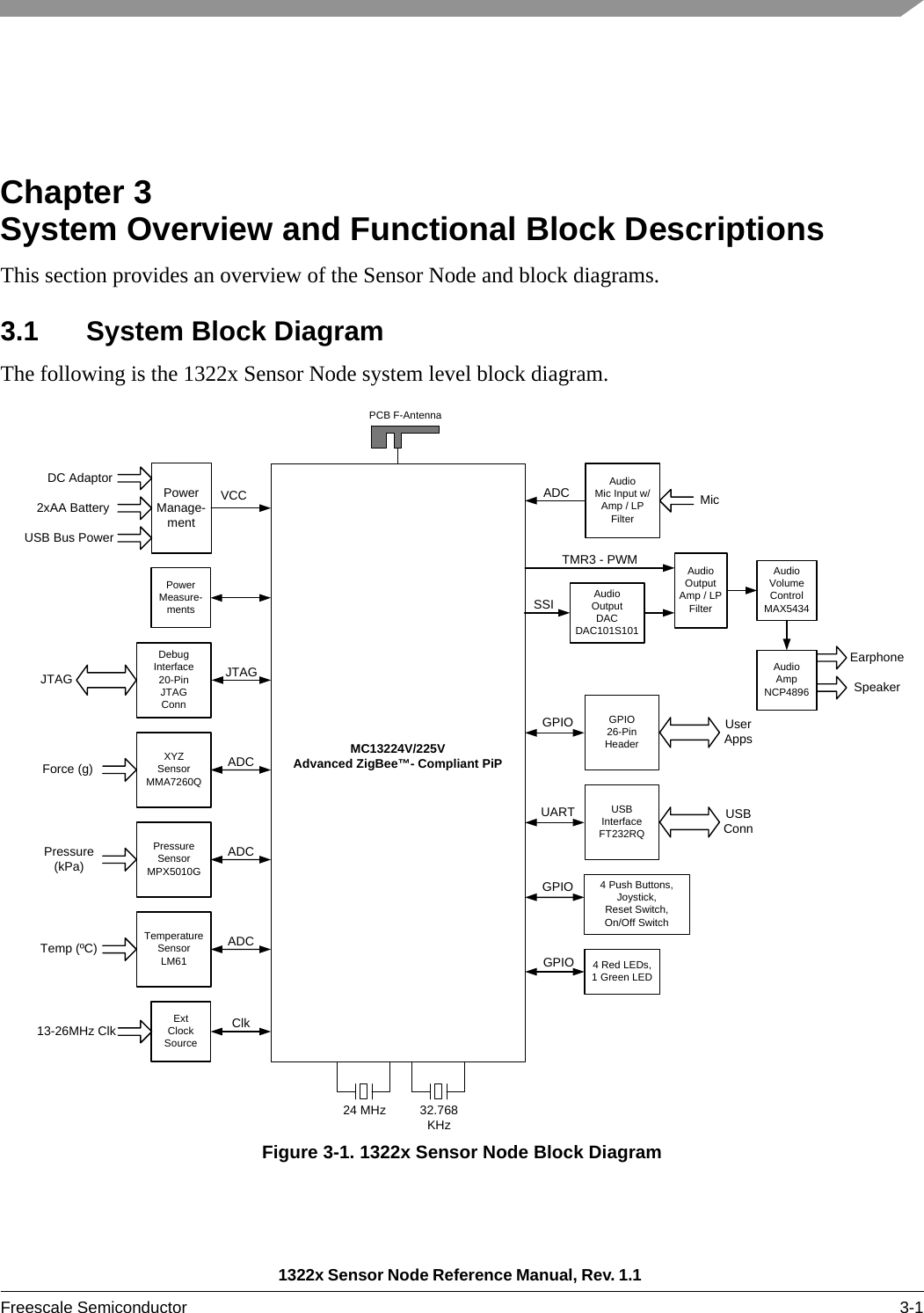
![System Overview and Functional Block Descriptions1322x Sensor Node Reference Manual, Rev. 1.1 3-6 Freescale Semiconductor3.8.2 Pressure SensorThe pressure sensor is a Freescale Semiconductor MPXV5010GC6U fully integrated device. It provides a high level analog output signal that is proportional to the applied pressure. Its accuracy is ±5%, and its output voltage is typically 0.200 Vdc at 0 offset pressure with a slope of +450 mV/kPa (1.0 kPa [kiloPascal] equals 0.145 psi.). The sensor requires only one ADC input and is constantly powered .The pressure sensor has an axial port (upright tube) for connecting tubing for a pressure source. The outside dimension of the tube is 3.0 mm nominal, and the tube is accessible through the top of the plastic enclosure.3.8.3 Three-axis AccelerometerThe three-axis accelerometer is the MMA7260QR2 device from Freescale Semiconductor. The MMA7260QR2 is specified for sensitivity in four ranges (1.5g/2g/4g/6g). The range is selectable via control lines. Consult the data sheet for sensitivity and other information. Each axis requires an ADC input (three total), and the accelerometer can be powered down.3.9 Audio SubsystemThe audio subsystem provides means for simple output sounds/tones or for TELCO voice quality audio.• A 2.5mm stereo jack is provided to interface to a typical telephone-type headset with an electret microphone and a single earphone.• Audio input - The audio input is taken from the headset electret microphone (mic).— An onboard 10 k-ohm resistor circuit biases the mic for an ~1 Vdc operating voltage.— The mic AC signal is filtered and amplified through a active low-pass filter with a voltage gain of about 30 (~30 dB). The filter topology is a multiple feedback (MFB) 3-pole, linear phase design. The target cutoff frequency is 3.6 kHz. The filter is intended as an anti-aliasing filter for sampled data.— The input amplifier output is sampled via the onboard MC1322x ADC. The sampling frequency is programmable.• Audio output source - The audio output can be sourced from both a serial 10-bit DAC and a PWM timer output.— The 10-bit serial DAC uses the SSI port to send provide the digital sample data.— The PWM timer output is typically modulated to create a Class-D amplifier. Secondarily, a simple 50% duty cycle signal can provide simple tones.— The audio output source is jumper selectable via J7• Audio output processing - The DAC or PWM out signal is filtered through an active 2-pole LPF. From the filter the signal passes through a passive attenuator, and then is amplified and driven to either an on-board speaker or the headset earphone.— The attenuator provides a volume control that is controlled via a software 32 linear tap programmable, non-volatile digital potentiometer. The interface to the potentiometer is the I2C port.](https://usermanual.wiki/Freescale-Semiconductor/1322X-SRB/User-Guide-976032-Page-18.png)