Freescale Semiconductor 1323X-MRB Developer Board User Manual 1323xDHRM
Freescale Semiconductor, Inc. Developer Board 1323xDHRM
Contents
- 1. User Manual 1
- 2. User Manual 2
User Manual 1

Document Number: 1323xDHRM
Rev. 1.0
04/2011
1323x Development Hardware
Reference Manual

How to Reach Us:
Home Page:
www.freescale.com
E-mail:
support@freescale.com
USA/Europe or Locations Not Listed:
Freescale Semiconductor
Technical Information Center, CH370
1300 N. Alma School Road
Chandler, Arizona 85224
+1-800-521-6274 or +1-480-768-2130
support@freescale.com
Europe, Middle East, and Africa:
Freescale Halbleiter Deutschland GmbH
Technical Information Center
Schatzbogen 7
81829 Muenchen, Germany
+44 1296 380 456 (English)
+46 8 52200080 (English)
+49 89 92103 559 (German)
+33 1 69 35 48 48 (French)
support@freescale.com
Japan:
Freescale Semiconductor Japan Ltd.
Headquarters
ARCO Tower 15F
1-8-1, Shimo-Meguro, Meguro-ku,
Tokyo 153-0064, Japan
0120 191014 or +81 3 5437 9125
support.japan@freescale.com
Asia/Pacific:
Freescale Semiconductor Hong Kong Ltd.
Technical Information Center
2 Dai King Street
Tai Po Industrial Estate
Tai Po, N.T., Hong Kong
+800 2666 8080
support.asia@freescale.com
For Literature Requests Only:
Freescale Semiconductor Literature Distribution Center
P.O. Box 5405
Denver, Colorado 80217
1-800-521-6274 or 303-675-2140
Fax: 303-675-2150
LDCForFreescaleSemiconductor@hibbertgroup.com
Information in this document is provided solely to enable system and software implementers to use
Freescale Semiconductor products. There are no express or implied copyright licenses granted
hereunder to design or fabricate any integrated circuits or integrated circuits based on the information
in this document.
Freescale Semiconductor reserves the right to make changes without further notice to any products
herein. Freescale Semiconductor makes no warranty, representation or guarantee regarding the
suitability of its products for any particular purpose, nor does Freescale Semiconductor assume any
liability arising out of the application or use of any product or circuit, and specifically disclaims any
and all liability, including without limitation consequential or incidental damages. “Typical” parameters
that may be provided in Freescale Semiconductor data sheets and/or specifications can and do vary
in different applications and actual performance may vary over time. All operating parameters,
including “Typicals”, must be validated for each customer application by customer’s technical
experts. Freescale Semiconductor does not convey any license under its patent rights nor the rights
of others. Freescale Semiconductor products are not designed, intended, or authorized for use as
components in systems intended for surgical implant into the body, or other applications intended to
support or sustain life, or for any other application in which the failure of the Freescale Semiconductor
product could create a situation where personal injury or death may occur. Should Buyer purchase
or use Freescale Semiconductor products for any such unintended or unauthorized application,
Buyer shall indemnify and hold Freescale Semiconductor and its officers, employees, subsidiaries,
affiliates, and distributors harmless against all claims, costs, damages, and expenses, and
reasonable attorney fees arising out of, directly or indirectly, any claim of personal injury or death
associated with such unintended or unauthorized use, even if such claim alleges that Freescale
Semiconductor was negligent regarding the design or manufacture of the part.
Freescale™ and the Freescale logo are trademarks of Freescale Semiconductor, Inc. All other
product or service names are the property of their respective owners.
© Freescale Semiconductor, Inc. 2007, 2008, 2009, 2010. All rights reserved.

1323x Development Hardware Reference Manual, Rev. 1.0
Freescale Semiconductor i
Contents
About This Book
Audience . . . . . . . . . . . . . . . . . . . . . . . . . . . . . . . . . . . . . . . . . . . . . . . . . . . . . . . . . . . . . . . . . . . . iii
Organization . . . . . . . . . . . . . . . . . . . . . . . . . . . . . . . . . . . . . . . . . . . . . . . . . . . . . . . . . . . . . . . . . iii
Revision History . . . . . . . . . . . . . . . . . . . . . . . . . . . . . . . . . . . . . . . . . . . . . . . . . . . . . . . . . . . . . . iii
Chapter 1
Safety Information
1.1 FCC Guidelines. . . . . . . . . . . . . . . . . . . . . . . . . . . . . . . . . . . . . . . . . . . . . . . . . . . . . . . . . . . . . . 1-1
1.1.1 Labeling . . . . . . . . . . . . . . . . . . . . . . . . . . . . . . . . . . . . . . . . . . . . . . . . . . . . . . . . . . . . . . . . 1-1
1.1.2 Operating Conditions . . . . . . . . . . . . . . . . . . . . . . . . . . . . . . . . . . . . . . . . . . . . . . . . . . . . . . 1-1
1.1.3 Exposure Limits . . . . . . . . . . . . . . . . . . . . . . . . . . . . . . . . . . . . . . . . . . . . . . . . . . . . . . . . . . 1-1
1.1.4 Antenna Restrictions. . . . . . . . . . . . . . . . . . . . . . . . . . . . . . . . . . . . . . . . . . . . . . . . . . . . . . . 1-1
1.2 Regulatory Approval For Canada (IC RSS 210) . . . . . . . . . . . . . . . . . . . . . . . . . . . . . . . . . . . . 1-2
1.2.1 26 PART 5 – Appendix . . . . . . . . . . . . . . . . . . . . . . . . . . . . . . . . . . . . . . . . . . . . . . . . . . . . 1-2
1.3 Electrostatic Discharge Considerations . . . . . . . . . . . . . . . . . . . . . . . . . . . . . . . . . . . . . . . . . . . 1-2
1.4 Disposal Instructions. . . . . . . . . . . . . . . . . . . . . . . . . . . . . . . . . . . . . . . . . . . . . . . . . . . . . . . . . . 1-2
Chapter 2
MC1323x Development Platform Overview and Description
2.1 Introduction. . . . . . . . . . . . . . . . . . . . . . . . . . . . . . . . . . . . . . . . . . . . . . . . . . . . . . . . . . . . . . . . . 2-1
2.2 Features. . . . . . . . . . . . . . . . . . . . . . . . . . . . . . . . . . . . . . . . . . . . . . . . . . . . . . . . . . . . . . . . . . . . 2-2
2.3 Driver Considerations . . . . . . . . . . . . . . . . . . . . . . . . . . . . . . . . . . . . . . . . . . . . . . . . . . . . . . . . . 2-5
2.4 General System Specifications . . . . . . . . . . . . . . . . . . . . . . . . . . . . . . . . . . . . . . . . . . . . . . . . . . 2-5
Chapter 3
1323x-Modular Reference Board
3.1 1323x-MRB Overview . . . . . . . . . . . . . . . . . . . . . . . . . . . . . . . . . . . . . . . . . . . . . . . . . . . . . . . . 3-1
3.1.1 Features. . . . . . . . . . . . . . . . . . . . . . . . . . . . . . . . . . . . . . . . . . . . . . . . . . . . . . . . . . . . . . . . . 3-1
3.1.2 Form Factor. . . . . . . . . . . . . . . . . . . . . . . . . . . . . . . . . . . . . . . . . . . . . . . . . . . . . . . . . . . . . . 3-2
3.1.3 Board Level Specifications. . . . . . . . . . . . . . . . . . . . . . . . . . . . . . . . . . . . . . . . . . . . . . . . . . 3-4
3.2 Functional Description . . . . . . . . . . . . . . . . . . . . . . . . . . . . . . . . . . . . . . . . . . . . . . . . . . . . . . . . 3-5
3.2.1 RF Performance and Considerations . . . . . . . . . . . . . . . . . . . . . . . . . . . . . . . . . . . . . . . . . . 3-6
3.2.2 Clocks . . . . . . . . . . . . . . . . . . . . . . . . . . . . . . . . . . . . . . . . . . . . . . . . . . . . . . . . . . . . . . . . . . 3-7
3.3 Reset and BDM Debug Port . . . . . . . . . . . . . . . . . . . . . . . . . . . . . . . . . . . . . . . . . . . . . . . . . . . . 3-8
3.3.1 Power Management . . . . . . . . . . . . . . . . . . . . . . . . . . . . . . . . . . . . . . . . . . . . . . . . . . . . . . . 3-9
3.3.2 IO Connectors J2 and J3 . . . . . . . . . . . . . . . . . . . . . . . . . . . . . . . . . . . . . . . . . . . . . . . . . . . 3-11
3.3.3 1323x-MRB Onboard Peripheral Functions . . . . . . . . . . . . . . . . . . . . . . . . . . . . . . . . . . . . 3-13
3.4 Schematic, Board Layout, and Bill of Material . . . . . . . . . . . . . . . . . . . . . . . . . . . . . . . . . . . . 3-15
3.4.1 Bill of Materials . . . . . . . . . . . . . . . . . . . . . . . . . . . . . . . . . . . . . . . . . . . . . . . . . . . . . . . . . 3-18
Chapter 4

1323x Development Hardware Reference Manual, Rev. 1.0
ii Freescale Semiconductor
1323x Remote Control Motherboard
4.1 1323x-RCM Overview . . . . . . . . . . . . . . . . . . . . . . . . . . . . . . . . . . . . . . . . . . . . . . . . . . . . . . . . 4-1
4.1.1 Features. . . . . . . . . . . . . . . . . . . . . . . . . . . . . . . . . . . . . . . . . . . . . . . . . . . . . . . . . . . . . . . . . 4-1
4.1.2 Form Factor. . . . . . . . . . . . . . . . . . . . . . . . . . . . . . . . . . . . . . . . . . . . . . . . . . . . . . . . . . . . . . 4-2
4.1.3 Board Level Specifications. . . . . . . . . . . . . . . . . . . . . . . . . . . . . . . . . . . . . . . . . . . . . . . . . . 4-3
4.2 Functional Description . . . . . . . . . . . . . . . . . . . . . . . . . . . . . . . . . . . . . . . . . . . . . . . . . . . . . . . . 4-4
4.2.1 Power Management . . . . . . . . . . . . . . . . . . . . . . . . . . . . . . . . . . . . . . . . . . . . . . . . . . . . . . . 4-5
4.2.2 GPIO Connection to 1323x-MRB . . . . . . . . . . . . . . . . . . . . . . . . . . . . . . . . . . . . . . . . . . . . 4-7
4.2.3 1323x-RCM Onboard Peripheral Functions . . . . . . . . . . . . . . . . . . . . . . . . . . . . . . . . . . . . 4-10
4.3 Schematic, Board Layout, and Bill of Material . . . . . . . . . . . . . . . . . . . . . . . . . . . . . . . . . . . . 4-14
4.3.1 1323x-RCM Bill of Materials. . . . . . . . . . . . . . . . . . . . . . . . . . . . . . . . . . . . . . . . . . . . . . . 4-21
Chapter 5
1323x Remote Extender Motherboard
5.1 1323x-REM Overview . . . . . . . . . . . . . . . . . . . . . . . . . . . . . . . . . . . . . . . . . . . . . . . . . . . . . . . . 5-1
5.1.1 Features. . . . . . . . . . . . . . . . . . . . . . . . . . . . . . . . . . . . . . . . . . . . . . . . . . . . . . . . . . . . . . . . . 5-1
5.1.2 Form Factor. . . . . . . . . . . . . . . . . . . . . . . . . . . . . . . . . . . . . . . . . . . . . . . . . . . . . . . . . . . . . . 5-2
5.1.3 Board Level Specifications. . . . . . . . . . . . . . . . . . . . . . . . . . . . . . . . . . . . . . . . . . . . . . . . . . 5-3
5.2 Functional Description . . . . . . . . . . . . . . . . . . . . . . . . . . . . . . . . . . . . . . . . . . . . . . . . . . . . . . . . 5-4
5.2.1 Power Management . . . . . . . . . . . . . . . . . . . . . . . . . . . . . . . . . . . . . . . . . . . . . . . . . . . . . . . 5-5
5.2.2 GPIO Connection to 1323x-MRB . . . . . . . . . . . . . . . . . . . . . . . . . . . . . . . . . . . . . . . . . . . . 5-7
5.2.3 1323x-REM Onboard Peripheral Functions . . . . . . . . . . . . . . . . . . . . . . . . . . . . . . . . . . . . . 5-9
5.2.4 USB Interface . . . . . . . . . . . . . . . . . . . . . . . . . . . . . . . . . . . . . . . . . . . . . . . . . . . . . . . . . . . 5-10
5.2.5 IR Receiver . . . . . . . . . . . . . . . . . . . . . . . . . . . . . . . . . . . . . . . . . . . . . . . . . . . . . . . . . . . . . 5-10
5.2.6 Pushbutton 2x4 Switch Matrix . . . . . . . . . . . . . . . . . . . . . . . . . . . . . . . . . . . . . . . . . . . . . . 5-11
5.2.7 Blue Indicator LEDs . . . . . . . . . . . . . . . . . . . . . . . . . . . . . . . . . . . . . . . . . . . . . . . . . . . . . . 5-11
5.3 Schematic, Board Layout, and Bill of Material . . . . . . . . . . . . . . . . . . . . . . . . . . . . . . . . . . . . 5-12
5.3.1 1323x-REM Bill of Materials . . . . . . . . . . . . . . . . . . . . . . . . . . . . . . . . . . . . . . . . . . . . . . . 5-16
Chapter 6
PCB Manufacturing Specifications
6.1 Single PCB Construction . . . . . . . . . . . . . . . . . . . . . . . . . . . . . . . . . . . . . . . . . . . . . . . . . . . . . . 6-1
6.2 Panelization. . . . . . . . . . . . . . . . . . . . . . . . . . . . . . . . . . . . . . . . . . . . . . . . . . . . . . . . . . . . . . . . . 6-3
6.3 Materials . . . . . . . . . . . . . . . . . . . . . . . . . . . . . . . . . . . . . . . . . . . . . . . . . . . . . . . . . . . . . . . . . . . 6-3
6.4 Solder Mask . . . . . . . . . . . . . . . . . . . . . . . . . . . . . . . . . . . . . . . . . . . . . . . . . . . . . . . . . . . . . . . . 6-3
6.5 Silk Screen . . . . . . . . . . . . . . . . . . . . . . . . . . . . . . . . . . . . . . . . . . . . . . . . . . . . . . . . . . . . . . . . . 6-4
6.6 Electrical PCB Testing . . . . . . . . . . . . . . . . . . . . . . . . . . . . . . . . . . . . . . . . . . . . . . . . . . . . . . . . 6-4
6.7 Packaging . . . . . . . . . . . . . . . . . . . . . . . . . . . . . . . . . . . . . . . . . . . . . . . . . . . . . . . . . . . . . . . . . . 6-4
6.8 Hole Specification/Tool Table . . . . . . . . . . . . . . . . . . . . . . . . . . . . . . . . . . . . . . . . . . . . . . . . . . 6-4
6.9 File Description. . . . . . . . . . . . . . . . . . . . . . . . . . . . . . . . . . . . . . . . . . . . . . . . . . . . . . . . . . . . . . 6-4

1323x Development Hardware Reference Manual, Rev. 1.0
Freescale Semiconductor iii
About This Book
This manual describes Freescale’s MC1323x development platform hardware. The MC1323x
development platform is an IEEE 802.15.4 compliant evaluation environment based on the Freescale
MC1323x device. The heart of the MC1323x platform is Freescale’s low cost System-on-Chip (SoC) for
the IEEE® 802.15.4 Standard that incorporates a complete, low power, 2.4 GHz radio frequency
transceiver with Tx/Rx switch, an 8-bit HCS08 CPU, and a functional set of MCU peripherals into a 48-pin
LGA package. This family of products is targeted for wireless RF remote control and other cost-sensitive
applications ranging from home TV and entertainment systems such as ZigBee BeeStack Consumer
(RF4CE) to low cost, low power, IEEE 802.15.4 and ZigBee end nodes.
Audience
This manual is intended for system designers.
Organization
This document is organized into 6 chapters.
Chapter 1 Safety Information — Highlights some of the FCC requirements.
Chapter 2 HCS08 Development Platform Overview and Description — Provides an
overview of the three boards that comprise the MC1323x development platform.
Chapter 3 Modular Reference Board — This chapter details the 1323x-MRB which is an
IEEE, 802.15.4 compliant evaluation board based on the Freescale MC1323x
device.
Chapter 4 1323x-Remote Control Module — This chapter details the 1323x-RCM
motherboard that accepts the 1323x-Modular Reference Board (1323x-MRB)
plug-in module (daughter card) and supplies a power supply and a rich set of
interface peripherals.
Chapter 5 1323x-Remote Extender Board — This chapter details the 1323x REM
motherboard that accepts the 1323x-Modular Reference Board (1323x-MRB)
plug-in module (daughter card) and supplies a power supply and set of interface
peripherals.
Chapter 6 PCB Manufacturing Specifications — This chapter provides the specifications
used to manufacture the various MC1323x printed circuit boards (PCBs).
Revision History
The following table summarizes revisions to this document since the previous release (Rev 0.0).
Revision History
Location Revision
Entire document Edited Chapter 1, Table 3-1, Table 4-1, Table 5-1, Section 4.2.1 and Section 5.2.1.

1323x Development Hardware Reference Manual, Rev. 1.0
iv Freescale Semiconductor
Definitions, Acronyms, and Abbreviations
The following list defines the acronyms and abbreviations used in this document.
ADC Analog to Digital Converter
AES Advanced Encryption Standard
ARM Advanced RISC Machine
CTS Clear to Send
DAC Digital to Analog Converter
DMA Direct Memory Access
I2C Inter-Integrated Circuit is a multi-master serial computer bus
ISM Industrial Scientific Medical 2.4 GHz radio frequency band
JTAG Joint Test Action Group
LGA Land Grid Array
MAC Media Access Controller
MCU Microcontroller Unit
NEXUS An embedded processor development tool interface that helps design engineers
identify software and hardware-level issues.
PCB Printed circuit board
PiP Platform in Package
PWM Pulse-width modulation
RCM Remote Control Module
REM Remote Extender Board
RTS Request to Send
SMA Connector SubMiniature version “A” connector
SPI Serial Peripheral Interface
SSI Synchronous Serial Interface
TACT Switch A switch that provides a slight “snap” or “click” to the user to indicate function.
TELCO Telephone Company
USB Universal Serial Bus
VCP Virtual Com Port

1323x Development Hardware Reference Manual, Rev. 1.0
Freescale Semiconductor 1-1
Chapter 1
Safety Information
1.1 FCC Guidelines
This equipment is for use by developers for evaluation purposes only and must not be incorporated into
any other device or system. This device may not be sold to the general public. Integrators will be
responsible for reevaluating the end product (including the transmitter) and obtaining a separate FCC
authorization.
FCC approval of this device only covers the original configuration of this device as supplied. Any
modifications to this product, including changes shown in this manual, may violate the rules of the Federal
Communications Commission and Industry Canada and make operation of the product unlawful.
1.1.1 Labeling
FCC labels are physically located on the back of the board.
1.1.2 Operating Conditions
This device complies with part 15 of the FCC Rules. Operation is subject to the following two conditions:
• This device may not cause harmful interference.
• This device must accept any interference received, including interference that may cause undesired
operation.
1.1.3 Exposure Limits
This equipment complies with FCC radiation exposure limits set forth for an uncontrolled environment.
The antenna(s) used for this equipment must be installed to provide a separation distance of at least 8
inches (20cm) from all persons.
1.1.4 Antenna Restrictions
An intentional radiator shall be designed to ensure that no antenna other than that furnished by the
responsible party shall be used with the device. The use of a permanently attached antenna or of an
antenna that uses a unique coupling to the intentional radiator shall be considered sufficient to comply with
the provisions of this Section. The manufacturer may design the unit so that a broken antenna can be
replaced by the user, but the use of a standard antenna jack or electrical connector is prohibited. This
requirement does not apply to carrier current devices or to devices operated under the provisions of
Sections 15.211, 15.213, 15.217, 15.219, or 15.221. Further, this requirement does not apply to intentional

Safety Information
1323x Development Hardware Reference Manual, Rev. 1.0
1-2 Freescale Semiconductor
radiators that must be professionally installed, such as perimeter protection systems and some field
disturbance sensors, or to other intentional radiators which, in accordance with Section 15.31(d), must be
measured at the installation site. However, the installer shall be responsible for ensuring that the proper
antenna is employed so that the limits in this Part are not exceeded.
1.2 Regulatory Approval For Canada (IC RSS 210)
This device complies with Industry Canada licence-exempt RSS standard(s). Operation is subject to the
following two conditions:
1. This device may not cause interference, and
2. This device must accept any interference, including interference that may cause undesired
operation of the device.
1.2.1 26 PART 5 – Appendix
Le présent appareil est conforme aux CNR d'Industrie Canada applicables aux appareils radio exempts de
licence. L'exploitation est autorisée aux deux conditions suivantes:
1. l'appareil ne doit pas produire de brouillage, et
2. l'utilisateur de l'appareil doit accepter tout brouillage radioélectrique subi, même si le brouillage
est susceptible d'en compromettre le fonctionnement.
1.3 Electrostatic Discharge Considerations
Although damage from electrostatic discharge (ESD) is much less common on these devices than on early
CMOS circuits, normal handling precautions should be used to avoid exposure to static discharge.
Qualification tests are performed to ensure that these devices can withstand exposure to reasonable levels
of static without suffering any permanent damage.
All ESD testing is in conformity with the JESD22 Stress Test Qualification for Commercial Grade
Integrated Circuits. During the device qualification ESD stresses were performed for the human body
model (HBM), the machine model (MM) and the charge device model (CDM).
All latch-up test testing is in conformity with the JESD78 IC Latch-Up Test.
When operating or handling the development boards or components, Freescale strongly recommends
using at least the grounding wrist straps plus any or all of the following ESD dissipation methods:
• Flexible fabric, solid fixed size, or disposable ESD wrist straps
• Static control workstations, static control monitors and table or floor static control systems
• Static control packaging and transportation materials and environmental systems
1.4 Disposal Instructions
This product may be subject to special disposal requirements. For product disposal instructions, refer to
www.freescale.com/productdisposal.

1323x Development Hardware Reference Manual, Rev. 1.0
Freescale Semiconductor 2-1
Chapter 2
MC1323x Development Platform Overview and Description
2.1 Introduction
The MC1323x development platform is an IEEE 802.15.4 compliant evaluation environment based on the
Freescale MC1323x device. The heart of the MC1323x platform is Freescale’s low cost System-on-Chip
(SoC) for the IEEE® 802.15.4 Standard that incorporates a complete, low power, 2.4 GHz radio frequency
transceiver with Tx/Rx switch, an 8-bit HCS08 CPU, and a functional set of MCU peripherals into a 48-pin
LGA package. This family of products is targeted for wireless RF remote control and other cost-sensitive
applications ranging from home TV and entertainment systems such as ZigBee BeeStack Consumer
(RF4CE) to low cost, low power, IEEE 802.15.4 and ZigBee end nodes.
The MC1323x development platform is comprised of three boards:
• 1323x-Modular Reference Board (1323x-MRB) - this board contains the MC1323x device with 32
MHz reference oscillator crystal, RF circuitry including antenna, and supporting circuitry. The
board can be used as a simple standalone evaluation platform or as a daughter card to the other
MC1323x development platform boards or to a custom, application specific motherboard. See
Chapter 3, “1323x-Modular Reference Board” for detailed information.
— Provides compact reference design for device footprint and RF layout
— Provides pre-designed MC1323x hardware (device and function)
— Provides access to the MC1323x full set of GPIO
— Provides MCU BDM debug port
— Provides optional local 2 Mbit serial FLASH, 32.768 kHz oscillator crystal, IR “blaster” LED
and power management.
• 1323x-Remote Control Motherboard (1323x-RCM) - this board accepts the 1323x-MRB as a
plug-in module (daughter card) and supplies a variety of peripheral functions to the MC1323x
through the IO connectors. The peripheral functions are targeted primarily to a consumer TV or
entertainment remote control application. See Chapter 4, “1323x Remote Control Motherboard”
for detailed information.
— Provides 36-switch matrix for remote control pushbuttons
— USB <> serial interface for communication to a PC and provides board power
— Touchpad for user interface
— Onboard 128 x 32 pixel graphic LCD for menus and host feedback - a unique feature to
RF-based remote controls
— Accelerometer for motion detection and game play
• 1323x-Remote Extender Motherboard (1323x-REM) - this board also accepts the 1323x-MRB
plug-in module (daughter card) and supplies a very simple set of peripheral functionality. See
MC1323x Development Platform Overview and Description
1323x Development Hardware Reference Manual, Rev. 1.0
2-2 Freescale Semiconductor
Chapter 5, “1323x Remote Extender Motherboard” for detailed information. A small 8-switch
matrix, IR receiver, and USB interface provides means for communication to the MC1323x for:
— Simple keypad-only applications
— Connection to a PC
— Host connection such as for a remote control extender or remote control receiver
Whether the 1323x-MRB is used in a simple standalone application or in combination with another host
card, Freescale provides a complete software development environment called the Freescale BeeKit
Wireless Connectivity Toolkit (BeeKit). BeeKit is a comprehensive codebase of wireless networking
libraries, application templates, and sample applications. The BeeKit Graphical User Interface (GUI)
allows users to create, modify, and update various wireless networking implementations. A wide range of
software functionality is available to complement the 1323x-MRB and these are provided as codebases
within BeeKit.
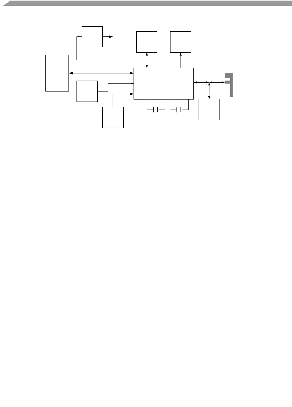
2.2 Features
The MC1323x development platform is built around the concept of having a single daughter card
(1323x-MRB) that contains the MC1323x IC and all necessary I/O connections for use as a self-contained
module or for connection to an application motherboard. Figure 2-1 shows a simplified block diagram of
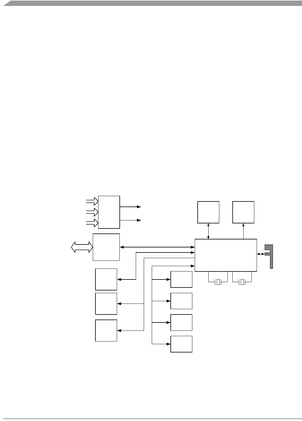
the more powerful Freescale configuration of the 1323x-MRB combined with the 1323x-RCM.
Figure 2-1. Simplified RCM+MRB Block Diagram
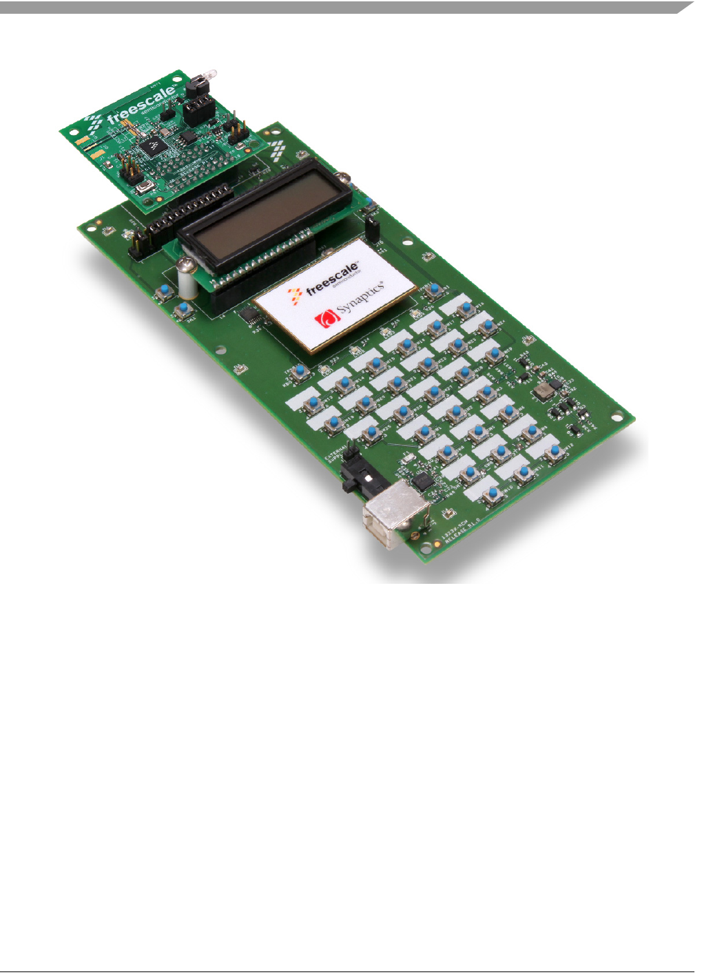
Figure 2-2 shows a photo of the combined boards with the 1323x-MRB mounted on the 1323x-RCM.
32 MHz 32.768
KHz
Power
Manage-
ment
DC Supply
2xAA Battery
VDD
MC13233
QFN
BDM
Debug
Port
3-Axis
Acceler-
ometer
USB
Interface
FT232RQ
UARTUSB
Conn
6x6
Switch
Matrix
PCB
F-Antenna
USB
IIC
Touchpad
V_LCD
2 Mbit
Serial
FLASH
GPIO
128x32
Graphic
LCD
Buzzer
4 LED
Indicators
IR
Blaster
SPI
MC1323x Development Platform Overview and Description
1323x Development Hardware Reference Manual, Rev. 1.0
Freescale Semiconductor 2-3
Figure 2-2. 1323x-MRB Mounted on the 1323x-RCM
Features of the MC1323x development platform include:
• Full IEEE 802.15.4 compliant wireless node; ZigBee capable with Freescale’s BeeStack software
stack
• Based on Freescale’s low-cost MC1323x IEEE® 802.15.4 SoC platform which incorporates a
complete, low power, 2.4 GHz radio frequency transceiver with Tx/Rx switch, an 8-bit HCS08
CPU, and a functional set of MCU peripherals into a 48-pin LGA package
• Reference design area with small footprint, low cost RF node
— Integrated transmit/receive switch
— Differential input/output port (typically used with a balun)
— Low external component count
— Programmable output power with 0 dBm nominal output power, programmable from -30 dBm
to +3 dBm typical
— Receive sensitivity of -93 dBm (typical) at 1% PER, 20-byte packet, much better than the IEEE
802.15.4 Standard of -85 dBm

MC1323x Development Platform Overview and Description
1323x Development Hardware Reference Manual, Rev. 1.0
2-4 Freescale Semiconductor
— Onboard printed metal F-Antenna
• 32 MHz reference oscillator
• BDM serial MCU debug port
• Optional secondary 32.768 kHz crystal oscillator for accurate low power timing
• IR blaster
• 2 Mbit serial FLASH (uses SPI interface)
• Master reset switch
• Full power regulation and management
• 1323x-MRB board provides
— Required circuitry for MC13233 - crystals and RF circuitry including F-Antenna and optional
SMA connector
— Local power supply regulation
— Access to all GPIO
— Standalone or daughter card use models
— Serial FLASH, IR blaster, and BDM functions
• 1323x-RCM when used with 1323x-MRB provides
— USB to UART serial interface that is USB bus-powered and full-speed compatible to the USB
2.0 and 1.1 specifications
— Power supply source from two AA batteries, USB connector, or DC source
— 128x32 pixel graphic LCD
— 3-axis Accelerometer (uses IIC interface)
— Touch pad interface with interrupt capability (uses IIC interface)
— 6x6 Switch matrix
— Single tone buzzer
— 4 Blue LED indicators
• 1323x-REM when used with 1323x-MRB provides
— USB to UART serial interface that is USB bus-powered and full-speed compatible to the USB
2.0 and 1.1 specifications
— Power supply source from two AA batteries, USB connector, or DC source
— IR receiver
— 4x2 Switch matrix
— 4 Blue LED indicators
MC1323x Development Platform Overview and Description
1323x Development Hardware Reference Manual, Rev. 1.0
Freescale Semiconductor 2-5
2.3 Driver Considerations
When users first connect a 1323x-RCM or 1323x-REM based platform to a PC, they may be prompted to
install drivers. If BeeKit is installed and this occurs, do not allow Windows to automatically search for and
install the drivers. Instead, select manual installation and steer Windows to the following directory:
C:\Program Files\Freescale\Drivers
If installing the BeeKit software package to another drive or directory, indicate the Drivers directory
created by the installer in the custom location where BeeKit was installed.
Follow the instructions as they appear on the screen to complete driver installation.
If BeeKit is not installed, be aware of the following:
• The boards use the FTDI serial to USB converter, Virtual COM Port (VCP) driver for Windows,
available at www.ftdichip.com/ftdrivers.htm.
(Direct (D2XX) drivers are also available.)
• The FTDI web site offers drivers for other platforms including Windows® (98 through Vista x64
and CE), MAC OS (8 through X) and Linux.
• Download the appropriate driver and follow the instructions to complete driver installation.
2.4 General System Specifications
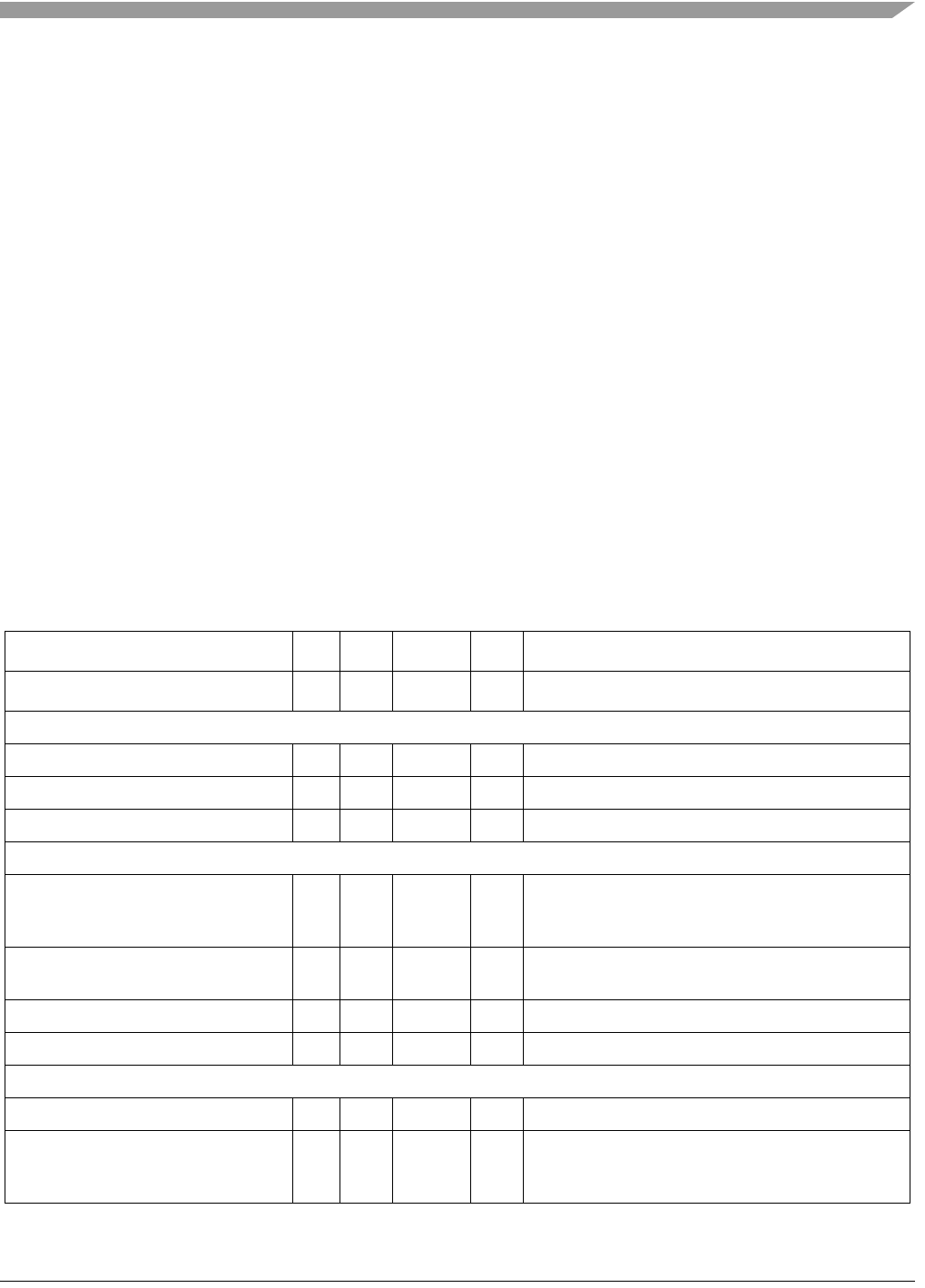
Table 2-1. MC1323x Platform Specifications
Parameter Units Notes/Conditions
MIN TYP MAX
Power
Voltage supply (DC) 2.5 5 6 V When using REM or RCM
Voltage supply (USB) 4.4 5 5.25 V USB 2.0/1.1 standard specification
Voltage supply (Batteries) 2.8 3.2 V
Temperature
Operating temperature; non-battery
operation (see note)
-20 +25 +70 °C Operating temperature is limited to +70 °C due to
switches. Basic circuit is good for a maximum
temperature of +85 °C.
Operating temperature; battery
operation (see note)
0 +25 +50 °C Operating temperature is limited by battery
temperature range
Storage temperature -30 +25 +70 °C
USB interface USB 2.0 and 1.1 full-speed compatible
RF (1323x-MRB)
802.15.4 Frequency range 2405 2480 MHz All 16 channels in the 2450 MHz band
Range (outdoor / line of sight) 300 Meter <1% PER for 20-byte packets (point-to-point in
communications with 1322X Sensor Reference
Board)
MC1323x Development Platform Overview and Description
1323x Development Hardware Reference Manual, Rev. 1.0
2-6 Freescale Semiconductor
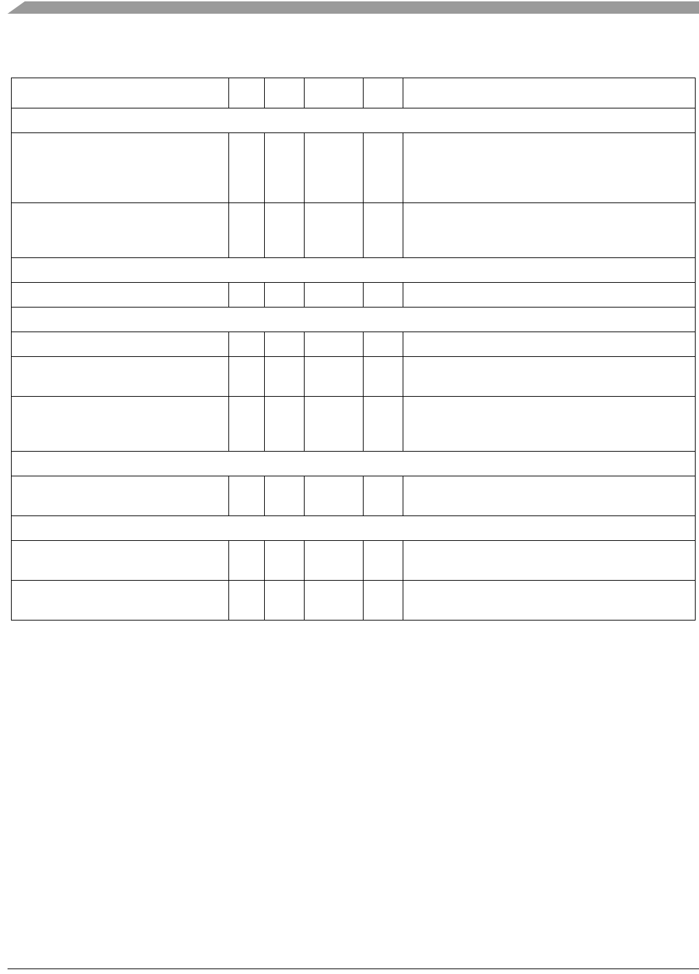
RF Transmitter
802.15.4 Output power -30 0 +3 dBm Over range of Pout from IC control in 2 dB steps.
Note: On channel 26, output power should not
exceed -5 dBm (power setting 0x0E) to meet
FCC Part 15 requirements.
Harmonics
2nd harmonics
3rd harmonics
-30?
-30?
dBm
dBm
Harmonics are compliant to ETSI and FCC
regulatory approval standards
RF Receiver
802.15.4 sensitivity -93 dBm <1% PER for 20-byte packets
Regulatory Approval
FCC Not yet certified.
CE (ETSI) Product is approved accordingly to the EN 300 328
V1.7.1 (2006-10) standard
CE (EMC) Product is approved accordingly to the EN 301 489-1
V1.6.1 (2005-09) and EN 301 489-17 V1.2.1
(2002-08) standards
Safety
UL Product is approved accordingly to the IEC 60950-1
and EN 60950-1, First Edition standards
Environment
RoHS Product complies with the EU Directive 2002/95/EC
of 27 January 2003
WEEE Product complies with the EU Directive 2002/95/EC
of 27 January 2003
Table 2-1. MC1323x Platform Specifications
Parameter Units Notes/Conditions

1323x Development Hardware Reference Manual, Rev. 1.0
Freescale Semiconductor 3-1
Chapter 3
1323x-Modular Reference Board
3.1 1323x-MRB Overview
The 1323x-Modular Reference Board (1323x-MRB) is an IEEE 802.15.4 compliant evaluation board
based on the Freescale MC1323x device. The 1323x-MRB provides a platform to evaluate the MC1323x
device, develop software and applications, and demonstrate IEEE 802.15.4 based networking capabilities.
The core device is accompanied by the 32 MHz reference oscillator crystal, RF circuitry including
antenna, and supporting circuitry.
This basic board is intended as the core module for MC1323x evaluation and application development and
can be used in the following modes:
• Simple standalone evaluation platform
• Daughtercard to the other MC1323x Development Platform boards (1323x-RCM or 1323x-REM)
• Daughtercard to an application specific motherboard.
3.1.1 Features
The 1323x-MRB provides the following features:
• Small form factor (2 x 2 inches)
• 4-Layer metal, 0.034 inch thick FR4 board
• MC1323x reference design area
— LGA footprint and power supply bypass
— 32 MHz reference oscillator crystal
— RF components and layout
• Low cost RF node
— Integrated transmit/receive switch
— Differential input/output port (typically used with a balun)
— Programmable output power with 0 dBm nominal output power, programmable from -30 dBm
to +3 dBm typical
— Receive sensitivity of -93 dBm (typical) at 1% PER, 20-byte packet
— Printed metal F-Antenna
• 32.768 kHz crystal provided for optional timing oscillator
• Two connectors provided daughter card mounting
— 20-Pin primary connector
1323x-Modular Reference Board
1323x Development Hardware Reference Manual, Rev. 1.0
3-2 Freescale Semiconductor
— 18-Pin secondary connector
— Provide main supply voltage to board
— Provide access to all MC1323x GPIO
• Flexible board power supply
— 3.3 V LDO series regulator supplied
— Regulator bypass jumper option
— Separate external voltage source option
— Power-on green LED
— Jumpers allow various block current measurements
• 6-Pin BDM serial MCU debug port
• MC1323x reset switch
• Onboard peripheral functions
— IR blaster (The MC1323x CMT port is employed as a GPIO to drive large IR blasters. For IR
blasters under 20ma, use the CMT port directly.)
— 2 Mbit serial FLASH (uses SPI interface)
3.1.2 Form Factor
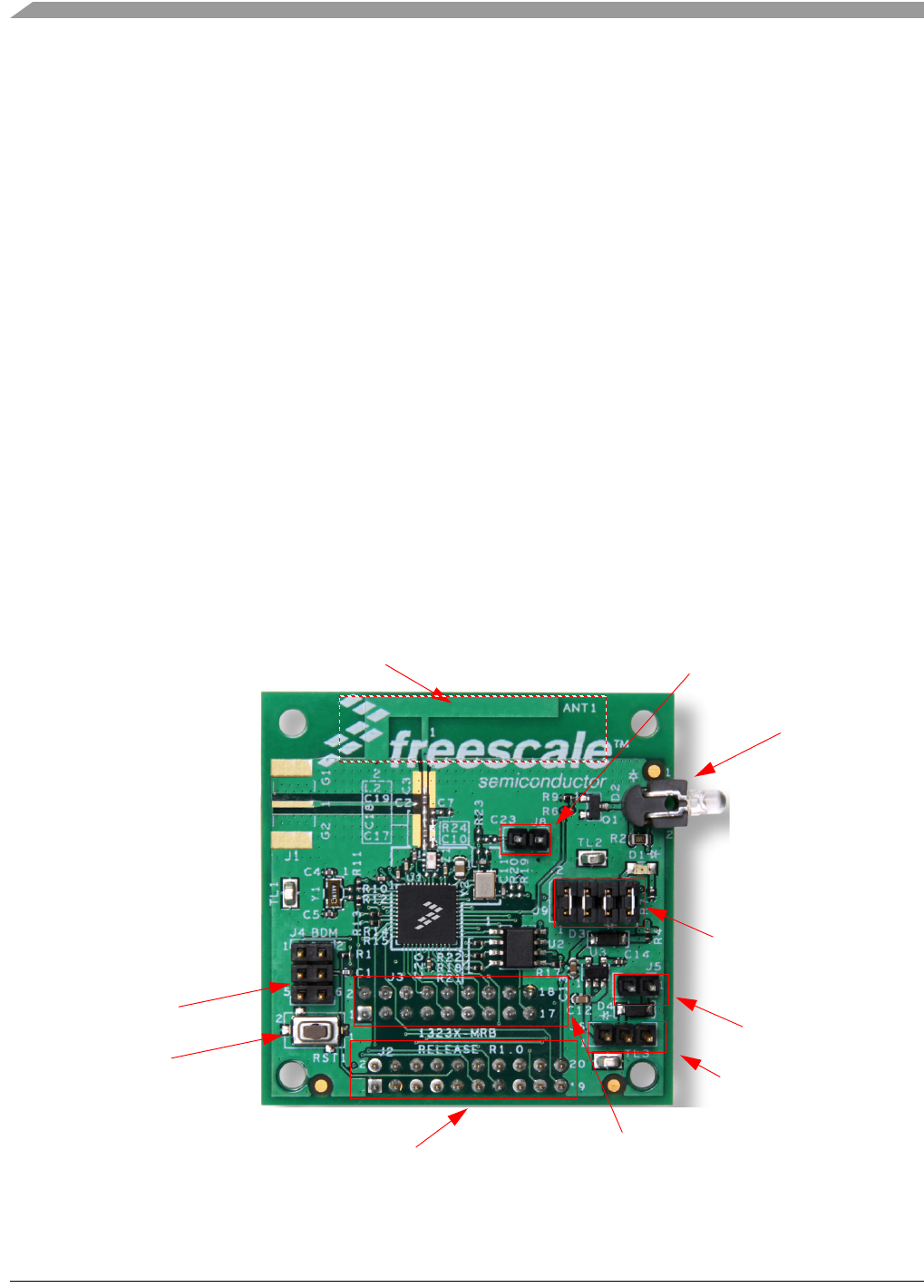
Figure 3-1 shows the 1323x-MRB connector and header locations.
Figure 3-1. 1323x-Modular Reference Board (1323x-MRB)
BDM Port
Reset Sw
Primary 20-Pin IO
Connector (J2)
J6
(J4) J5
Secondary 18-Pin IO
Connector (J3)
J9
J8
F-Antenna
IR Diode D2
1323x-Modular Reference Board
1323x Development Hardware Reference Manual, Rev. 1.0
Freescale Semiconductor 3-3
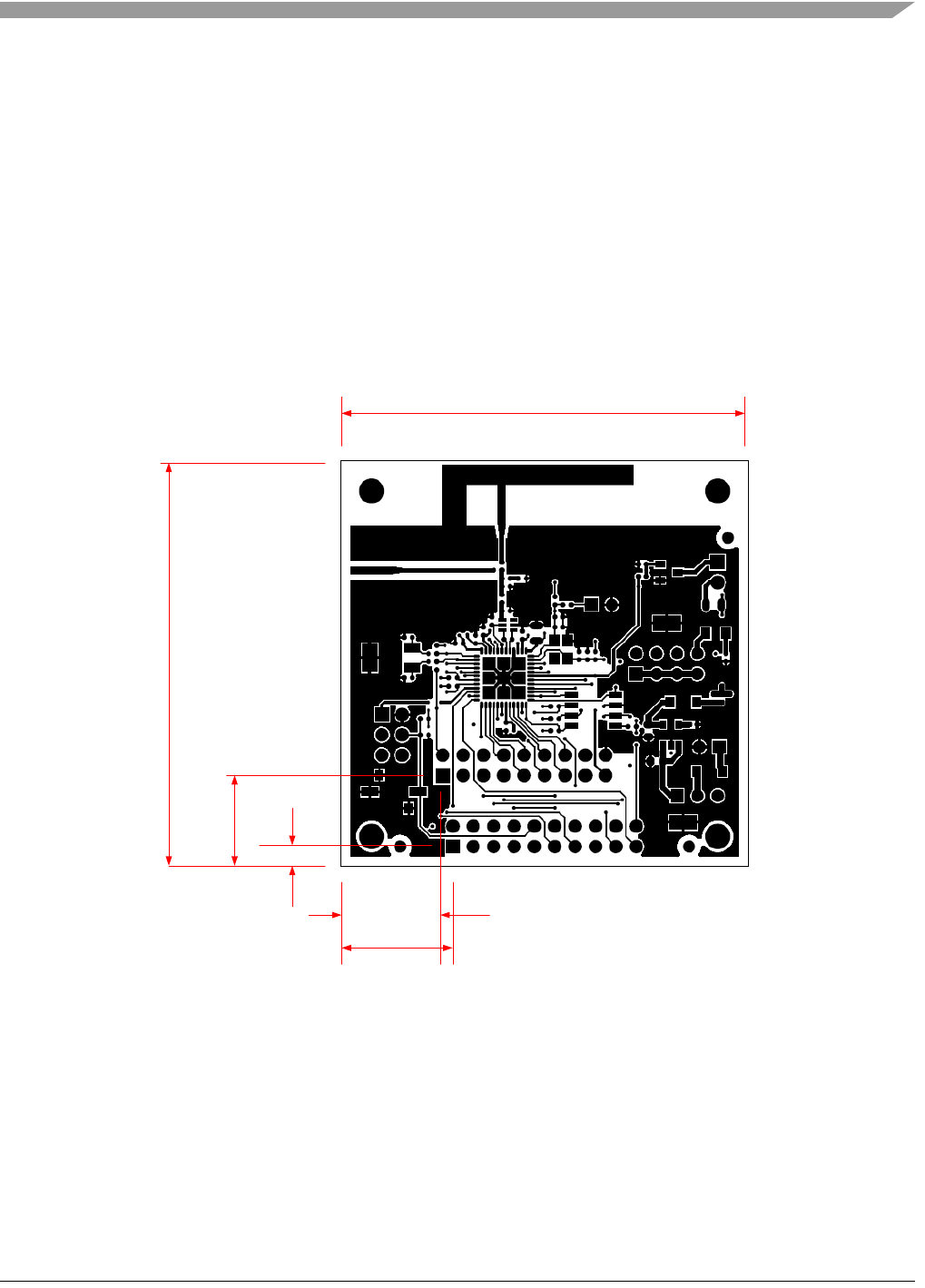
Figure 3-2 shows a footprint of the 1323x-MRB with the location of the IO Headers J2 and J3. The user
may desire to create a motherboard on which the 1323x-MRB would be mounted, and headers J2 and J3
are used for connection to the motherboard:
• Both headers have standard 0.10in / 2.54 mm pin spacing
• J2 is 20-pin and J3 is 18-pin
• Both are pin headers mounted on the bottom side of the 1323x-MRB and are intended to plug into
matching receptacles on the motherboard.
• It is recommended that 1323x-MRB be located such that it extends beyond edge of the
motherboard (see Figure 3-2) so that the entire F-Antenna is exposed with no motherboard ground
or voltage plane beneath it. This is to allow best results transmitting and receiving with the radio.
• With the 1323x-MRB oriented as shown in Figure 3-2, the IR blaster transmits to the right.
Figure 3-2. 1323x-MRB Top Side (Component Side) Footprint
2.01 in
2.01 in
0.45 in
0.10 in
0.49 in
0.55 in
1323x-Modular Reference Board
1323x Development Hardware Reference Manual, Rev. 1.0
3-4 Freescale Semiconductor
3.1.3 Board Level Specifications
Table 3-1. 1323x-MRB Specifications
Parameter Units Notes/Conditions
MIN TYP MAX
General
Size (PCB: X, Y) 51 x 51
2.01 x 2.01
mm
inches
Layer build (PCB) 0.8
0.034
mm
inches
4-Layer
Dielectric material (PCB) FR4
Power
Voltage supply (DC)
With 3.3 V regulator in use
Not using regulator with serial
FLASH and IR
Not using regulator with
MC1323x only
3.50
2.7
1.8
16
3.6
3.6
V Full module use
Not regulated - using all features
Lower voltage usable only by MC1323x
Current consumption TBD mA
Temperature
Operating temperature (see note) -20 +25 +70 °C • Operating temperature is limited to +70
°C due to switches. Basic circuit is good
for a maximum temperature of +85 °C.
• Operating temperature may also be
further limited when used in conjunction
with REM or RCM having a battery
supplied voltage source. See Ta b l e 4 - 1
and Table 5-1.
Storage temperature -30 +25 +70 °C
IR Transmitter
Current 63 mA
Range 10 m
RF
802.15.4 Frequency range 2405 2480 MHz All 16 channels in the 2450 MHz band
Range (outdoor / line of sight) 300 Meter <1% PER for 20-byte packets (point-to-point
in communications with 1323x Sensor
Reference Board)
RF Transmitter
802.15.4 Output power -30 0 +3 dBm
1323x-Modular Reference Board
1323x Development Hardware Reference Manual, Rev. 1.0
Freescale Semiconductor 3-5
3.2 Functional Description
The 1323x-MRB is built around Freescale’s MC1323x 48-pin LGA IEEE 802.15.4 platform. Figure 3-2
shows a simple block diagram. This board is intended as a simple evaluation platform and as a building
block for application development. The 4-layer board provides the MC1323x with its required RF
circuitry, 32 Mhz reference oscillator crystal, and power supply bypassing. The layout for this base level
functionality can be used as a reference layout by the user target board.
In additional to the base MC1323x functionality, the 1323x-MRB provides features to assist in debug, an
IR blaster, a 2 Mbit serial FLASH, reset button, simple power manager, and expansion connectors for the
GPIO. In the following sections, refer to:
•Figure 3-1 for location of connectors and features
•Figure 3-3 for the functional blocks
•Figure 3-11 for the board schematic
Harmonics
2nd harmonics
3rd harmonics
-38
-35
dBm
dBm
Harmonics are compliant to ETSI and FCC
regulatory approval standards
RF Receiver
802.15.4 sensitivity -93 dBm <1% PER for 20-byte packets
Regulatory Approval
FCC Product is approved accordingly to the FCC
part 15 standard
CE (ETSI) Product is approved accordingly to the EN
300 328 V1.7.1 (2006-10) standard
CE (EMC) Product is approved accordingly to the EN
301 489-1 V1.6.1 (2005-09) and EN 301
489-17 V1.2.1 (2002-08) standards
Safety
UL Product is approved accordingly to the IEC
60950-1 and EN 60950-1, First Edition
standards
Environment
RoHS Product complies with the EU Directive
2002/95/EC of 27 January 2003
WEEE Product complies with the EU Directive
2002/95/EC of 27 January 2003
Table 3-1. 1323x-MRB Specifications (continued)
Parameter Units Notes/Conditions
1323x-Modular Reference Board
1323x Development Hardware Reference Manual, Rev. 1.0
3-6 Freescale Semiconductor
Figure 3-3. 1323x-MRB Block Diagram
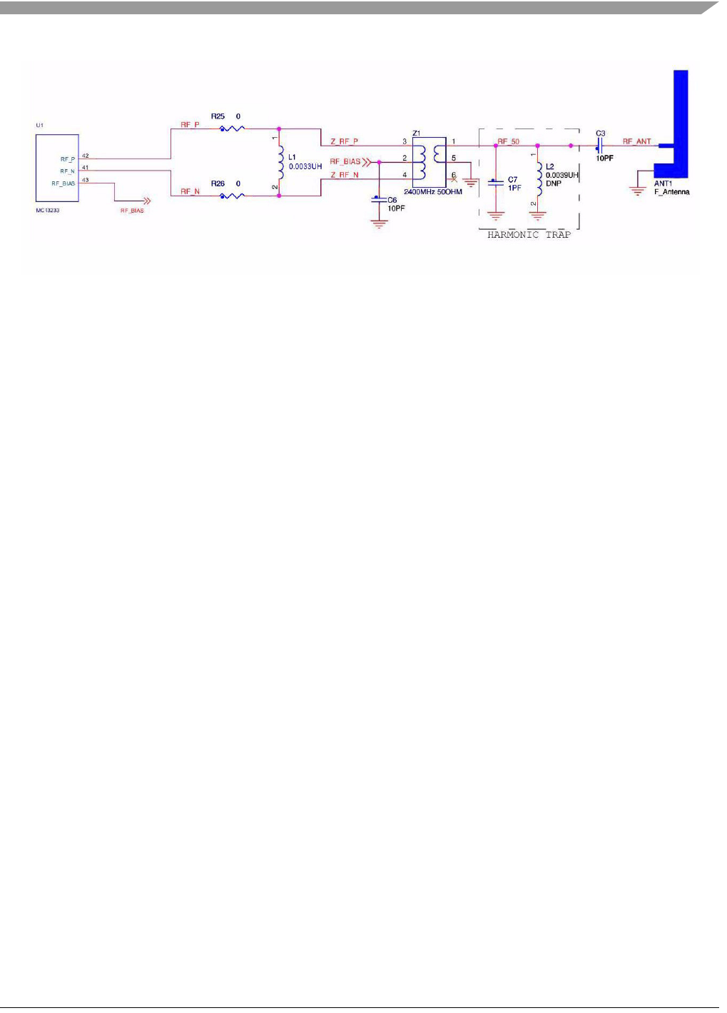
3.2.1 RF Performance and Considerations
The MC1323x transceiver includes a low noise amplifier, 1mW nominal output power, PA with internal
voltage controlled oscillator (VCO), integrated transmit/receive switch, on-board power supply regulation,
and full spread-spectrum encoding and decoding.
• Nominal output power is 0 dBm, with +3 dBm max
• Typical sensitivity is -93 dBm
• Frequency range is 2405 to 2480 MHz
• Typical range (outdoors, line of sight) is 130 meters
The 1323x Modular Reference Board utilizes a minimum number of components while providing good
RF performance:
• Uses a minimum number of RF matching components and external 50:100 balun
• “F” printed metal antenna for a small footprint, low cost design
An external 50 (unbal):100 (bal) balun connects a single-ended 50-Ω port to the differential RF port of the
MC1323x radio. The layout has provision for out-of-band signal suppression (components L2 and C7) if
required. Also note that control pin CT_Bias switches reference voltage to the balun as required for TX
(CT_Bias = 1.5V) or RX (CT_Bias = ground).
The default RF mode is use of the “F” antenna coupled through 10 pF C3 to the single-end RF port. An
alternative mode is to connect an SMA RF connector (not provided; must be mounted). This is useful for
connected measurements to test radio performance.
NOTE
See the MC1323x Data Sheet and Reference Manual for more RF design
information.
32 MHz 32.768
KHz
MC13233
QFN
BDM
Debug
Port
CMT
GPIO
SPI
IR
Blaster
LED
2 Mbit
Serial
FLASH
Reset
Button
GPIO
Headers
J2 & J3
Optional
SMA
Conn
F-Ant
Power
Manage-
ment
1323x-Modular Reference Board
1323x Development Hardware Reference Manual, Rev. 1.0
Freescale Semiconductor 3-7
Figure 3-4. 1323x-MRB RF Circuitry
3.2.2 Clocks
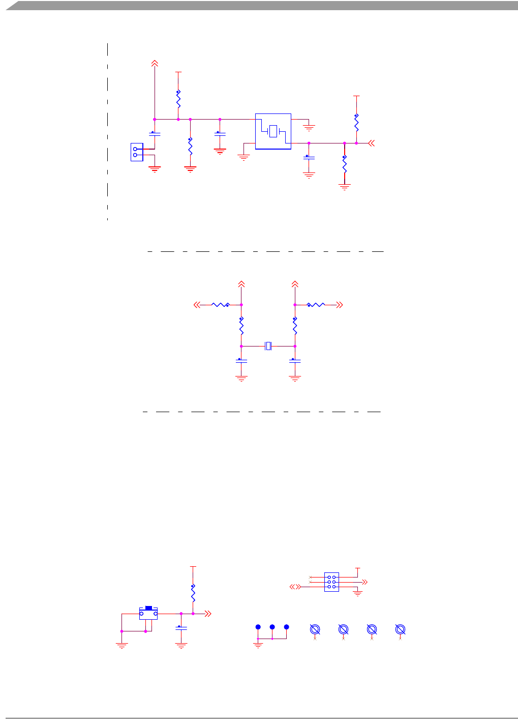
The MC1323x provides for two clocks:
• 32 MHz Reference Oscillator - Figure 3-5 shows the external 32 MHz external crystal Y2. This
mounted crystal must meet the MC1323x specifications. The IEEE 802.15.4 Standard requires that
the frequency be accurate to less that +/-40 ppm.
— Capacitors C10 and C11 provide the bulk of the crystal load capacitance. Onboard trim
capacitors can be programmed to center the frequency. At 25°C, it is desired to have the
frequency accurate to +/-10 ppm or less to allow for temperature variation.
— To measure the 32 MHz oscillator frequency, signal PTD7/XTAL_32MOUT can optionally be
programmed to provide a buffered output clock signal
— The 1323x-MRB has provision for injecting an external 32 MHz clock source as an alternative
to use of the onboard crystal:
– The crystal Y2 should be removed
– Resistors R23, R24, R19, and R20 must be mounted
– C23 must be mounted
– The external 32 MHz source is connected to 2-pin header J8; the frequency accuracy of the
external source must meet the +/-40 ppm of the IEEE 802.15.4
• Optional 32.768 kHz Crystal Oscillator - Provision is also made for a secondary 32.768 kHz crystal
X2 (see Figure 3-6). This oscillator can be used for a low power accurate time base.
— The module comes provided with this Y1 crystal and its load capacitors C4 and C15.
— Load capacitors C4 and C15 provide the entire crystal load capacitance; there is no onboard
trim capacitance.
— The 32 kHz oscillator components are supplied, but un-enabled. Zero-ohm resistors R11 and
R13 enable use of IO signals PTA0 and PTA1 via the IO connector and are supplied as mounted.
These must be unmounted and moved to resistor sites R10 and R12 to enable the 32.768 kHz
crystal and disable PTAO and PTA1.
1323x-Modular Reference Board
1323x Development Hardware Reference Manual, Rev. 1.0
3-8 Freescale Semiconductor
Figure 3-5. 1323x-MRB 32 MHz Reference Oscillator Circuit
Figure 3-6. 1323x-MRB 32.768 kHz Optional Oscillator Circuit
3.3 Reset and BDM Debug Port
The reset circuit and BDM port connector are shown in Figure 3-7. See Figure 3-1 for switch and header
locations.
• Reset switch RST2 is active low and provides a hardware reset to the MC1323x
• The 6-pin BDM 2x3 header J10 is provided to connect the MC1323x serial debug port to a standard
HC9S08 debug module.
Figure 3-7. 1323x-MRB Reset Switch and BDM Port
32MHz XTAL
V_IC
V_IC
XTAL_32M
EXTAL_32M
C10
12PF
C10
12PF
C11
12PF
C11
12PF
R24
1K
DNP
R24
1K
DNP
R19
1K
DNP
R19
1K
DNP
R20
1K
DNP
R20
1K
DNP
Y2
32MHZ
Y2
32MHZ
1 4
32
C23
10PF
DNP
C23
10PF
DNP
J8
HDR 1X2
J8
HDR 1X2
1
2
R23
1K
DNP
R23
1K
DNP
32kHz XTAL
MRB-PTA1MRB-PTA0
PTA1/EXTAL_32KPTA0/XTAL_32K
R13 0R13 0
Y1
32.768KHZ
Y1
32.768KHZ
21
C4
12PF
C4
12PF
R10
0
DNP
R10
0
DNP
R11 0R11 0
R12
0
DNP
R12
0
DNP
C5
12PF
C5
12PF
RESET
V_IC
MRB-RSTb
C1
1000pF
C1
1000pF
RST1
SW_MOM
RST1
SW_MOM
12
3
4
R1
15K
R1
15K
BDM
V_IC
BKGD
MRB-RSTb
BH1
125
BH1
125
TL1TL1 BH3
125
BH3
125
J4
HDR 2X3
J4
HDR 2X3
1 2
3 4
65
BH2
125
BH2
125
TL2TL2 BH4
125
BH4
125
TL3TL3
1323x-Modular Reference Board
1323x Development Hardware Reference Manual, Rev. 1.0
Freescale Semiconductor 3-9
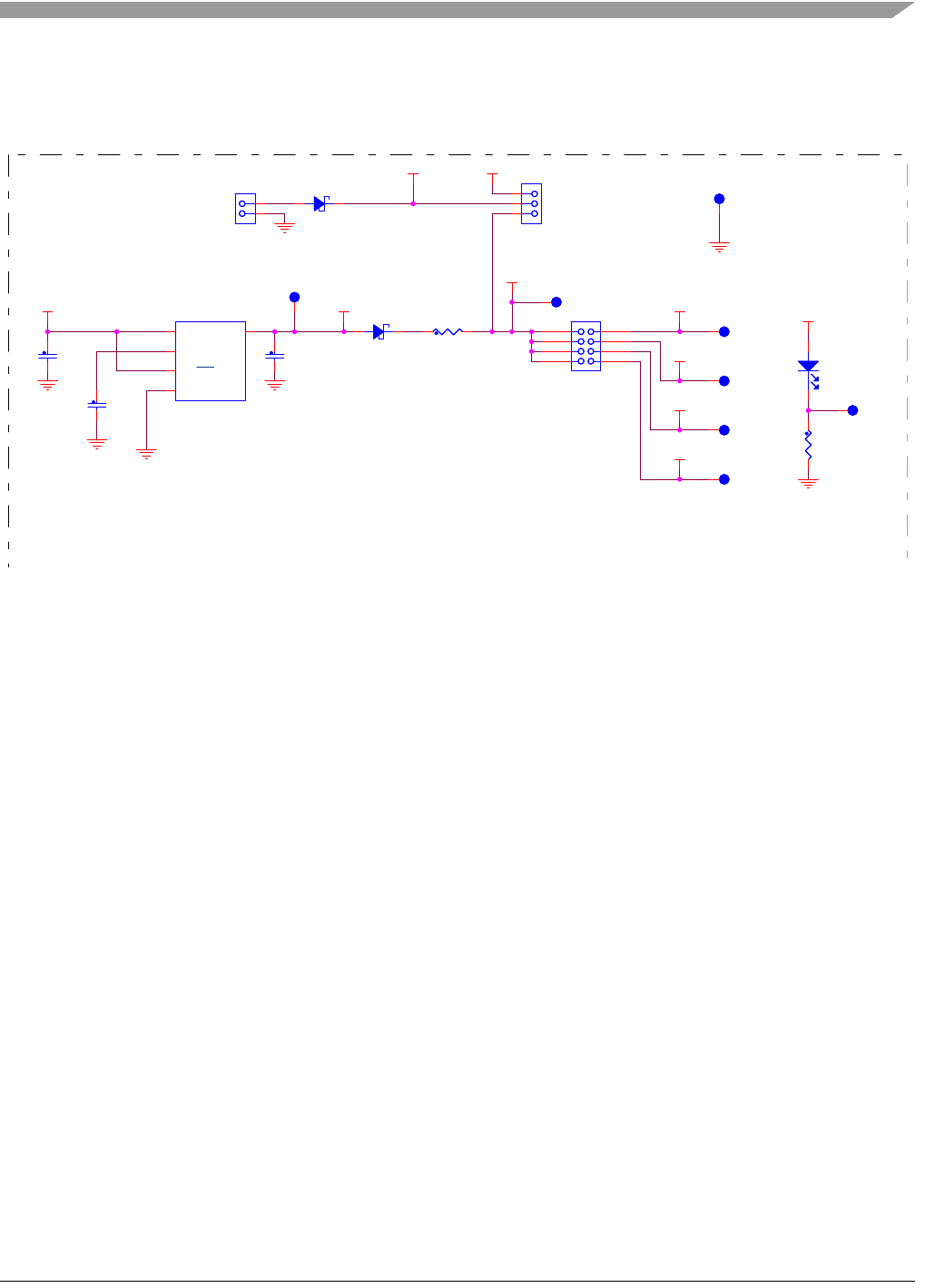
3.3.1 Power Management
The 1323x-MRB power management circuit is shown in Figure 3-8.
Figure 3-8. 1323x-MRB Power Management Circuit
Power to the 1323x-MRB can be configured in several ways and the circuit has the following features:
• Board can be supplied through the IO headers (V_BRD)
• Board can be supplied from an external DC supply (J5)
— The external supply can be unregulated (V_UNREG) and make use of the onboard 3.3 V LDO
regulator
— The external supply voltage can be used directly without use of the LDO
• 8-Pin 2x4 header J9 provides means to supply current to various board components and also
measure current if desired
• Green LED D1 is available as a power indicator.
Table 3-2 shows the header configuration information for the various power supply modes.
NOTE
• The Freescale 1323x-RCM and 1323x-REM development boards
generate the system power supply on the motherboard and supply the
voltage to the 1323x-MRB through the V_BRD pin of Headers J2 and
J3. In this mode, the current flows to the 1323x-MRB through the pins.
• If an external supply is used via 1323x-MRB header J5, current flows to
the motherboard through the V_BRD pin of Headers J2 and J3. THE
MOTHERBOARD SUPPLY SHOULD NOT BE USED.
• In all modes, the IO voltage supply of peripherals on a motherboard
must be the same voltage as V_BRD, which is also the voltage applied
to the IC MC1323x.
POWER ON
3.3V LDO REGULATOR
J6:
»SHUNT 2->1 UNREGULATED EXTERNAL SUPPLY V_EXT > 3.3V
»SHUNT 3->2 ONLY IF V_EXT = 3V
»NO-SHUNT WHEN V_BRD USED AS SUPPLY THROUGH J9, PINS 3 & 4 SHUNTED
J5: EXTERNAL SUPPLY
POWER MANAGEMENT
VDD
V_LED
V_EXT
V_LDO
V_UNREG
V_LED
V_MEM
V_BRD
V_IC
V_UNREG
TP3TP3
TP6TP6
D1
GREEN
D1
GREEN
AC
TP13TP13
C12
1UF
C12
1UF
TP2TP2
TP5TP5
C13
2.2UF
C13
2.2UF
TP12TP12
J6
HDR TH 1X3
J6
HDR TH 1X3
1
2
3
TP1TP1
J9
HDR_2X4
J9
HDR_2X4
1 2
3 4
65
7 8
TP4TP4
R7
330
R7
330
D4
MBR0520LT1G
D4
MBR0520LT1G
2 1
U3
LP2985AIM5-3.3
U3
LP2985AIM5-3.3
VIN
1
GND
2
ON/OFF
3
BYP
4
VOUT 5
R4 0R4 0
C14
0.01UF
C14
0.01UF
D3
MBR0520LT1G
D3
MBR0520LT1G
2 1
J5
HDR 1X2
J5
HDR 1X2
1
2
1323x-Modular Reference Board
1323x Development Hardware Reference Manual, Rev. 1.0
3-10 Freescale Semiconductor
Header J9 provides means to disable different sub-circuits or measure current and connections are
described in Table 3-3. Current measurements can be made by inserting a current meter in place of a
designated jumper.
Table 3-2. 1323x-MRB Power Configurations
Mode Voltage
Range
External
Source
J5
Ext Mode
Select
J6
Current Enable
J9 Description
Source V_BRD 2.7 - 3.6 V1
1The MC1323x can run as low as 1.8 V, however, the serial FLASH and IR blaster require 2.7 V or greater
Not used Not used - all
pins open
Short Pins 3-4 -
short other desired
supplies
Normal Operation -
The 1323x-MRB main supply is
supplied by the motherboard
through the J2 and J3 Headers
External Source
- Using LDO
3.5 - 16 V Connected -
supplies
DC Voltage
Short Pins 1-2 Short pins for all
desired supplies
External voltage w/regulation -
• Input range is set by the LDO
regulator.
• 3.3 V is supplied to 1323x-MRB;
do not use motherboard supply
• J2 and J3 Headers supply
voltage to V_BRD pins when J9,
Pins 3-4 are shorted
External Source
- Not Using LDO
2.7 - 3.6 V1Connected -
supplies
DC Voltage
Short Pins 2-3 Short pins for all
desired supplies
External voltage w/o regulation -
• Input range is set by the onboard
circuitry
• 2.7 - 3.3 V is supplied to
1323x-MRB
• J2 and J3 Headers supply
voltage to V_BRD pins
Table 3-3. Power Distribution Header J9
Supply
Designation
Header
Pins Description
V_MEM 1 - 2 Supply voltage to serial FLASH memory -
• Jumper pins to supply memory.
• If memory is not powered, it can load MC1323x SPI port
V_BRD 3 - 4 Supply voltage connected to IO Connectors J2 and J3 -
• This supplies J2 and J3 if an external MRB supply is used
• This voltage supplies the MRB if the motherboard is the main power
• This connection is normally always jumpered
V_IC 5 - 6 Supply voltage to MC1323x -
• Normally jumpered
• Supplies only the MC1323x IC
• Normally always same voltage as V_BRD
V_LED 7 - 8 Supply voltage to power indicator LED and IR blaster LED -
• Jumper to use indicator or IR blaster
• Leave open for lowest power
1323x-Modular Reference Board
1323x Development Hardware Reference Manual, Rev. 1.0
Freescale Semiconductor 3-11
3.3.2 IO Connectors J2 and J3
The two IO connectors J2 and J3 are standard 100 mil pin headers mounted on the back (non-component
side) of the 1323x-MRB. The primary header J2 is 20-pin and the secondary header J3 is 18-pin, and they
are mounted physically in such a manner as to prevent reverse insertion of the 1323x-MRB into a
motherboard receptacle (see Figure 3-2). When the 1323x-RCM or 1323x-REM or custom motherboard
is plugged into these connectors, they allow access to MC1323x MCU GPIO.
• V_BRD is the connector supply voltage.
— Depending on power supply configuration, this voltage may supply the 1323x-MRB from the
motherboard or the 1323x-MRB may supply this voltage to the motherboard. See
Section 3.3.1, “Power Management”.
— Peripherals IO to the MC1323x and the MC1323x supply should use this same voltage
NOTE
The 1323x-RCM and 1323x-REM and 1323x-MRB are supplied configured
for the motherboard to supply main power.
• Some of the GPIO are shared with onboard devices. Check for the 1323x-MRB schematic and
Table 3-4 and Table 3-5 for any conflict.
• BDM port signal PTA7/BKGD is NOT connected to the IO headers to prevent possible interference
with the debug port.
Table 3-4. 20 Pin Connector
Header Pin
Number MC1323x Pin Name Description
1 V_BRD VDD supply to module
2 PTC5/SS SPI Bus Slave Select (SS) - shared with serial FLASH
3 GND Module ground
4 PTC7/MOSI SPI Bus MOSI signal - shared with serial FLASH
5 PTD5/RXD UART RXD input to MCU
6 PTC6/MISO SPI Bus MISO signal - shared with serial FLASH
7 PTD6/TXD UART TXD Output from MCU
8 PTC4/SPICLK SPI Clock (SPISCK) - shared with serial FLASH
9 PTD0/TPM0 GPIO / Timer IO
10 RESET Reset
11 PTA5/SDA I2C Bus data signal (SDA)
12 PTB7/KBI1P7 UART flow control RTS input into MCU (implemented in Freescale software)
13 PTA6/SCL I2C Bus clock signal (SCL)
14 PTD2/TPM2 UART flow control CTS output from MCU (implemented in Freescale software)
15 GND Module ground
16 PTD7/XTAL_32MOUT Port D Bit 7
1323x-Modular Reference Board
1323x Development Hardware Reference Manual, Rev. 1.0
3-12 Freescale Semiconductor
17 PTB0/KBI1P0 Port B Bit 0 / KBI1 Input Bit 0
18 PTB1/KBI1P1 Port B Bit 1 / KBI1 Input Bit 1
19 PTB2/KBI1P2 Port B Bit 2 / KBI1 Input Bit 2
20 PTB3/KBI1P3 Port B Bit 3 / KBI1 Input Bit 3
Table 3-5. 18 Pin Connector
Header Pin
Number MC1323x Pin Name Description
1 V_BRD VDD supply to module
2 PTA1/EXTAL_32K Port A Bit 1 - signal shared with 32.768 kHz oscillator
3 PTA0/XTAL_32K Port A Bit 0 - signal shared with 32.768 kHz oscillator
4 GND Module Ground
5 PTA2 Port A Bit 2 - MC1323x test mode enable; SPECIAL SIGNAL REFER TO
MC1323x Reference Manual
6 PTA3/IRQ Port A Bit 3 / IRQ (active low)
7 PTA4/XTAL_32KOUT Port A Bit 4 / optional buffered 32.768 kHz clock output
8 PTB4/KBI1P4 Port B Bit 4 / KBI1 Input Bit 4
9 PTB5/KBI1P5 Port B Bit 5 / KBI1 Input Bit 5
10 PTB6/KBI1P6 Port B Bit 6 / KBI1 Input Bit 6
11 PTC0/KBI2P0 Port C Bit 0 / KBI2 Input Bit 0
12 PTC1/KBI2P1 Port C Bit 1 / KBI2 Input Bit 1
13 PTC2/KBI2P2 Port C Bit 2 / KBI2 Input Bit 2
14 PTC3/KBI2P3 Port C Bit 3 / KBI2 Input Bit 3
15 PTD1/TPM1 Port D Bit 1/ TPM1
16 PTD3/TPM3 Port D Bit 3/ TPM3
17 PTD4/CMT Port D Bit 4/ CMT output - signal shared with IR blaster
18 GND Module ground
Table 3-4. 20 Pin Connector
Header Pin
Number MC1323x Pin Name Description
1323x-Modular Reference Board
1323x Development Hardware Reference Manual, Rev. 1.0
Freescale Semiconductor 3-13
3.3.3 1323x-MRB Onboard Peripheral Functions
The 1323x-MRB has two onboard peripheral functions to assist in implementing targeted applications.
NOTE
To use the peripherals, a minimum power supply voltage of 2.7 V must be
maintained.
3.3.3.1 2 Mbit Serial FLASH (SPI Interface)
Component U2 is an Atmel AT45DB021D 2 Mbit (256 kbyte) serial FLASH memory with SPI interface.
The memory is useful for over-the-air programming (OTAP) and for storage of non-volatile system data
or parameters. Figure 3-9 shows the memory circuit.
• Memory power supply is V_MEM (Header J9, Pin 1-2)
• Disabling the memory supply V_MEM may load the MC1323x SPI port through the U2 ESD
diodes
• Discrete pullup resistors for the SPI port are provided
• The SPI can be shared with another peripheral - an additional IO signal would be required as a chip
enable (CS or SS) for the peripheral. The normal SPI_SS and the second chip select should NOT
be active at the same time.
Figure 3-9. AT45DB021D 2 Mbit (256 kbyte) Serial FLASH memory
2MBit (256KB) FLASH
V_MEM
V_MEM V_MEMV_MEM
MRB-SPI_MISOMRB-SPI_MOSI
MRB-SPI_CLK
MRB-SPI_SS
R21
10K
R21
10K
R18
10K
R18
10K
U2
AT45DB021D
U2
AT45DB021D
SCK
2
VCC 6
WP 5
RESET
3
GND 7
CS
4
SI
1SO 8
R17
10K
R17
10K
R22
10K
R22
10K
1323x-Modular Reference Board
1323x Development Hardware Reference Manual, Rev. 1.0
3-14 Freescale Semiconductor
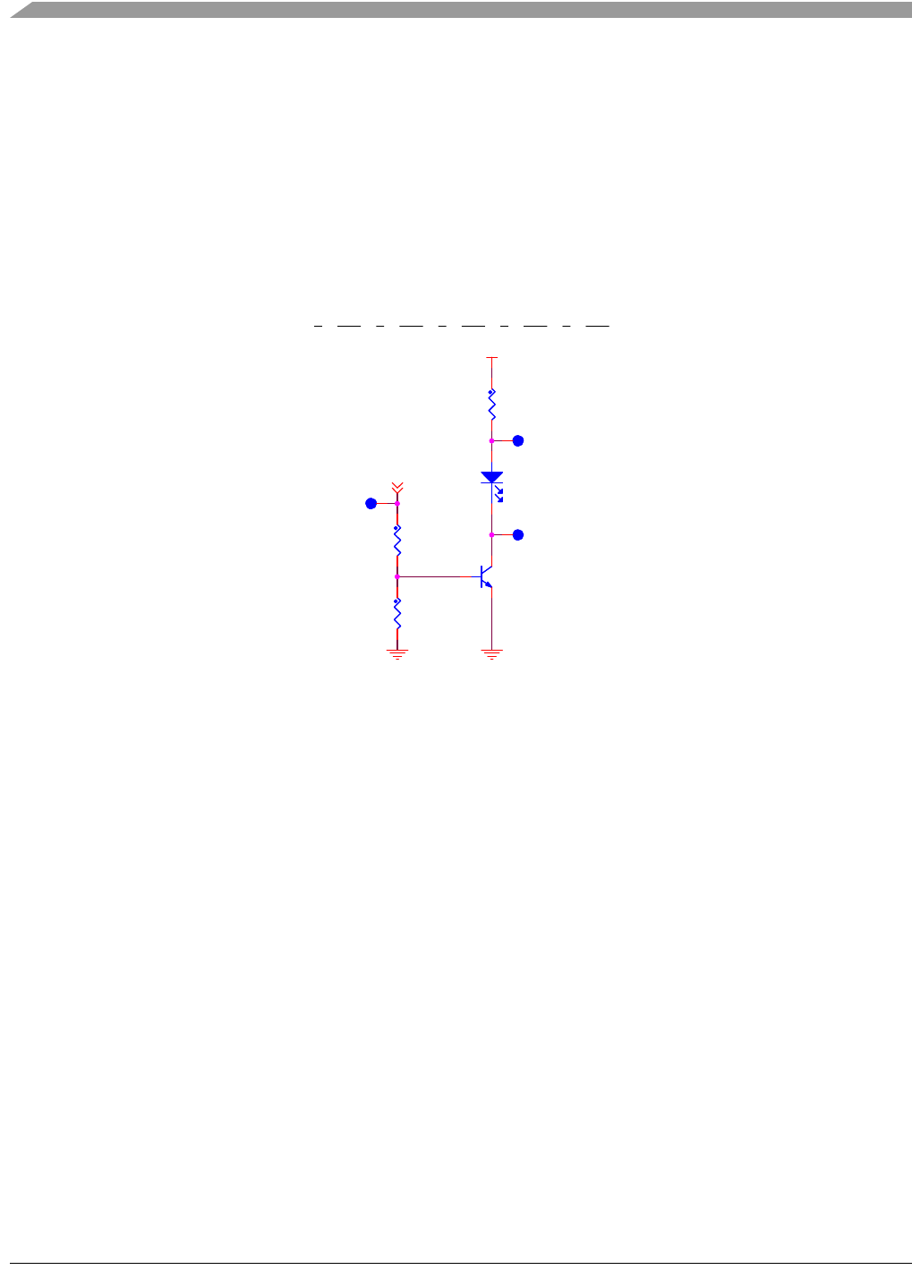
3.3.3.2 IR Transmitter (Blaster)
An IR transmitter or blaster is provided to control IR legacy components (see Figure 3-10).
• The IR power supply is V_LED (Header J9, Pin 7-8)
• The IR transmitter has approximately a 10 meter range.
• Current draw is approximately 80 mA when active.
• To reduce the peak current consumption, it is recommended that the IR transmitter only be active
when the MC1323x RF transceiver is in-active.
• When using the blaster in an application, observe proper orientation (see Figure 3-2)
Figure 3-10. IR Transmitter Circuit
INFRARED LED
V_LED
MRB-PTD4/CMT
R2
18.2
R2
18.2
TP9TP9
D2
VSLB3940
D2
VSLB3940
AC
R9
27K
R9
27K
R6
1.5K
R6
1.5K
TP8TP8
Q1
MMBT3904LT1G
Q1
MMBT3904LT1G
2 3
1
TP7TP7
1323x-Modular Reference Board
1323x Development Hardware Reference Manual, Rev. 1.0
Freescale Semiconductor 3-15
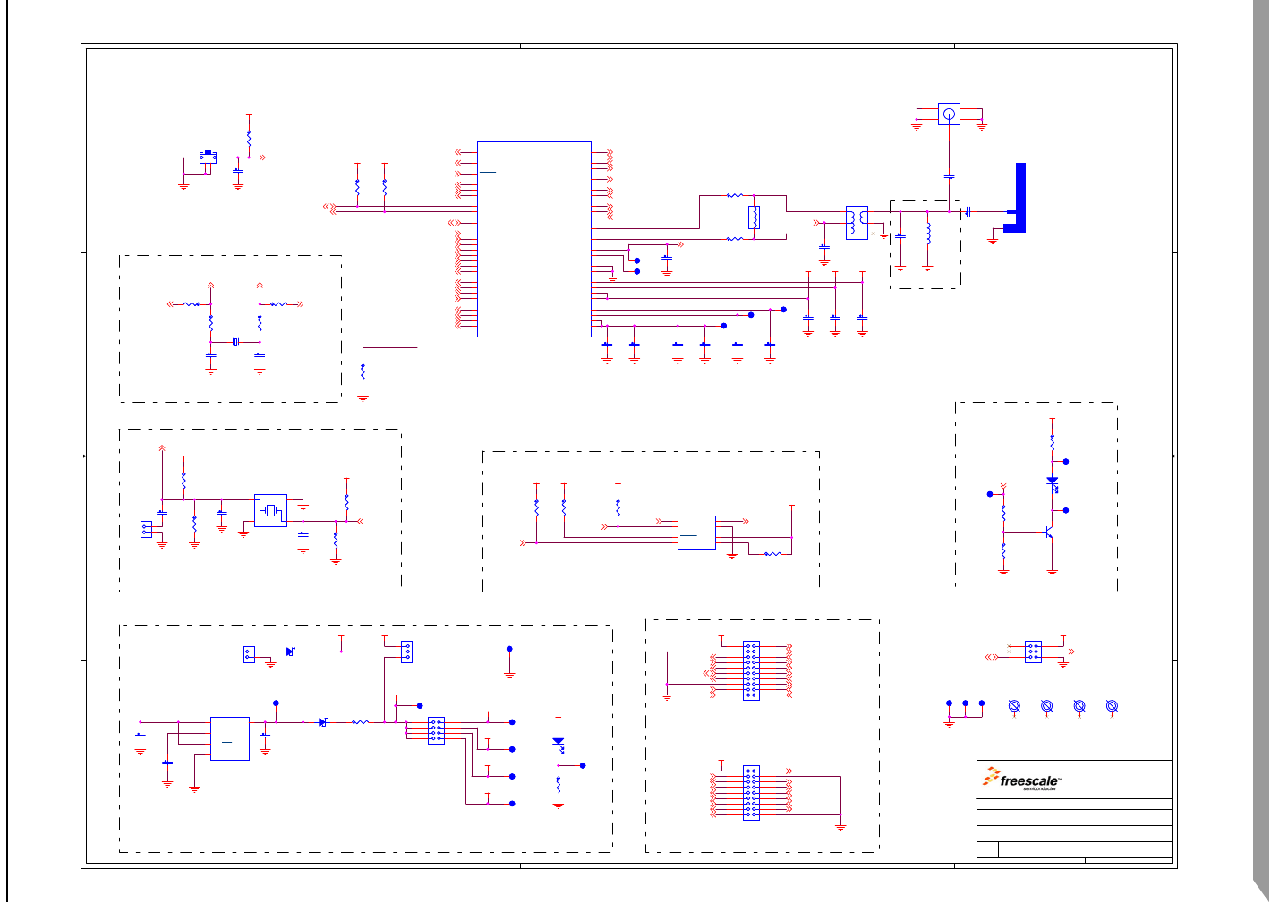
3.4 Schematic, Board Layout, and Bill of Material
Figure 3-11. 1323x-MRB Schematic
5
5
4
4
3
3
2
2
1
1
D D
C C
B B
A A
RESET
20-PIN GPIO
STANDARD HEADER
GPIO
POWER ON
3.3V LDO REGULATOR
INFRARED LED2MBit (256KB) FLASH
BDM
J6:
»SHUNT 2->1 UNREGULATED EXTERNAL SUPPLY V_EXT > 3.3V
»SHUNT 3->2 ONLY IF V_EXT = 3V
»NO-SHUNT WHEN V_BRD USED AS SUPPLY THROUGH J9, PINS 3 & 4 SHUNTED
HARMONIC TRAP
J5: EXTERNAL SUPPLY
POWER MANAGEMENT GPIO MAPPING
32MHz XTAL
32kHz XTAL
C8 & C28 PLACE
CLOSE TO U1.39
C18 & C26 PLACE
CLOSE TO U1.47
RF_SMA
RF_N
Z_RF_P
Z_RF_N
RF_ANT
RF_P
MRB-PTA2/LCD_CTL0
RF_50
V_IC
VDD
V_IC
V_LED
V_LED
V_IC
V_MEM
V_EXT V_BRD
V_BRD
V_LDO
V_UNREG
V_IC V_IC
V_MEM
V_IC
V_MEM
V_IC
V_IC
V_LED
V_MEM
V_BRD
V_IC
V_MEM
V_IC
V_UNREG
MRB-RSTb
XTAL_32M
BKGD
MRB-RSTb
MRB-SPI_MISOMRB-SPI_MOSI
MRB-SPI_CLK
MRB-SPI_SS
MRB-PTA1MRB-PTA0
PTA1/EXTAL_32KPTA0/XTAL_32K
RF_BIAS
RF_BIAS
MRB-KBI2P3
MRB-KBI2P2
PTA0/XTAL_32K
MRB-KBI2P1
MRB-KBI2P0
BKGD
MRB-I2C_SDA
MRB-RSTb
MRB-PTA4/32K_OUT
MRB-SPI_CLK
MRB-SPI_MOSI
MRB-I2C_SCL
MRB-PTA2/LCD_CTL0
MRB-SPI_MISO
MRB-SPI_SS
PTA1/EXTAL_32K
MRB-PTA3/IRQb
MRB-KBI1P0
MRB-KBI1P1
MRB-KBI1P2
MRB-KBI1P3
MRB-KBI1P4
MRB-KBI1P5
MRB-KBI1P6
MRB-UART_RTS/KBI1P7
MRB-PTD4/CMT
EXTAL_32M
XTAL_32M
MRB-PTD1/TPM1
MRB-UART_CTS/TPM2
MRB-PTD7
MRB-UART_TXD
MRB-UART_RXD
MRB-PTD3/TPM3
MRB-TPM0
EXTAL_32M
MRB-I2C_SCL
MRB-SPI_MOSI
MRB-SPI_SS
MRB-I2C_SDA
MRB-UART_RXD
MRB-UART_TXD
MRB-UART_CTS/TPM2
MRB-UART_RTS/KBI1P7
MRB-KBI1P2
MRB-KBI1P0
MRB-TPM0 MRB-RSTb
MRB-PTD7
MRB-SPI_CLK
MRB-KBI1P1
MRB-KBI1P3
MRB-SPI_MISO
MRB-PTD4/CMT
MRB-KBI1P5
MRB-PTA4/32K_OUT
MRB-KBI2P0
MRB-KBI1P4
MRB-KBI1P6
MRB-KBI2P1
MRB-KBI2P3
MRB-PTA3/IRQb
MRB-KBI2P2
MRB-PTA1
MRB-PTD1/TPM1
MRB-PTA0
MRB-PTA2/LCD_CTL0
MRB-PTD3/TPM3
MRB-PTD4/CMT
Drawing Title:
Size Document Number Rev
Date: Sheet of
Page Title:
ICAP Classification: FCP: FIUO: PUBI:
SCH-26115 PDF: SPF-26115 E4
1323X MODULAR REFERENCE BOARD
C
Thursday, February 10, 2011
MAIN SCHEMATIC
33
X ______
Drawing Title:
Size Document Number Rev
Date: Sheet of
Page Title:
ICAP Classification: FCP: FIUO: PUBI:
SCH-26115 PDF: SPF-26115 E4
1323X MODULAR REFERENCE BOARD
C
Thursday, February 10, 2011
MAIN SCHEMATIC
33
X ______
Drawing Title:
Size Document Number Rev
Date: Sheet of
Page Title:
ICAP Classification: FCP: FIUO: PUBI:
SCH-26115 PDF: SPF-26115 E4
1323X MODULAR REFERENCE BOARD
C
Thursday, February 10, 2011
MAIN SCHEMATIC
33
X ______
C10
12PF
C10
12PF
BH1
125
BH1
125
TP14TP14
C7
1PF
C7
1PF
L1
0.0033UH
L1
0.0033UH
12
TL1TL1
TP3TP3
BH3
125
BH3
125
R2
18.2
R2
18.2
C26
8.2PF
C26
8.2PF
C1
1000pF
C1
1000pF
R13 0R13 0
C25
8.2PF
C25
8.2PF
C22
0.22UF
C22
0.22UF
C11
12PF
C11
12PF
C3
10PF
C3
10PF
Y1
32.768KHZ
Y1
32.768KHZ
21
U1
MC1323X
U1
MC1323X
PTA0/XTAL_32K
1
PTA1/EXTAL_32K
2
RESET
3
PTA2
4
PTA3/IRQ
5
PTA4/XTAL_32K_OUT
6
PTA5/SDA
7
PTA6/SCL
8
PTA7/BKGD/MS
9
PTB0/KBI1P0
10
PTB1/KBI1P1
11
PTB2/KBI1P2
12
PTB3/KBI1P3
13
PTB4/KBI1P4
14
PTB5/KBI1P5
15
PTB6/KBI1P6
16
PTB7/KBI1P7
17
PTC0/KBI2P0
18
PTC1/KBI2P1
20
PTC2/KBI2P2
21
PTC3/KBI2P3
22
PTC4/SPICLK
23
PTC5/SS
24
PTC6/MISO
25
PTC7/MOSI
26
PTD0/TPM0 27
PTD1/TPM1 28
PTD2/TPM2 29
PTD3/TPM3 30
PTD4/CMT 31
PTD5/TXD 32
PTD6/RXD 33
PTD7/XTAL_32M_OUT 34
XTAL_32M 35
EXTAL_32M 36
RF_P 42
RF_N 41
NC 40
NC/TINJ_N 45
RF_BIAS/TINJ_P 43
PAD 49
VBATT_1 48
VBATT_2 44
VBATT_3 37
VBATT_4 19
VREG_VCO 38
VDD_ANA 39
VREG_LO2 46
VREG_ANA 47
TP10TP10
TP6TP6
D1
GREEN
D1
GREEN
AC
R25 0R25 0
R21
10K
R21
10K
J4
HDR 2X3
J4
HDR 2X3
1 2
3 4
65
C6
10PF
C6
10PF
J2
HDR_10X2
J2
HDR_10X2
1 2
3 4
65
7 8
910
11 12
13 14
15 16
17 18
19 20
TP13TP13
TP9TP9
C4
12PF
C4
12PF
C17
10PF
DNP
C17
10PF
DNP
C18
0.22UF
C18
0.22UF
D2
VSLB3940
D2
VSLB3940
AC
C12
1UF
C12
1UF
TP2TP2 BH2
125
BH2
125
RST1
SW_MOM
RST1
SW_MOM
12
3
4
R15
10K
R15
10K
R24
1K
DNP
R24
1K
DNP
R9
27K
R9
27K
TP16TP16
R1
15K
R1
15K
L2
0.0039UH
DNP
L2
0.0039UH
DNP
12
R19
1K
DNP
R19
1K
DNP
R20
1K
DNP
R20
1K
DNP
TP5TP5
Y2
32MHZ
Y2
32MHZ
1 4
32
C23
10PF
DNP
C23
10PF
DNP
R10
0
DNP
R10
0
DNP
R11 0R11 0
R6
1.5K
R6
1.5K
R14
10K
R14
10K
TL2TL2
C8
0.22UF
C8
0.22UF
C13
2.2UF
C13
2.2UF
J1
SMA_EDGE
J1
SMA_EDGE
1
G1 G3
G2 G4
TP12TP12
TP8TP8R18
10K
R18
10K
J6
HDR TH 1X3
J6
HDR TH 1X3
1
2
3
TP1TP1
C16
0.1UF
C16
0.1UF
C20
0.01UF
C20
0.01UF
C2
10PF
DNP
C2
10PF
DNP
R26 0R26 0
BH4
125
BH4
125
TP15TP15
R12
0
DNP
R12
0
DNP
ANT1
F_Antenna
ANT1
F_Antenna
U2
AT45DB021D
U2
AT45DB021D
SCK
2
VCC 6
WP 5
RESET
3
GND 7
CS
4
SI
1SO 8
Q1
MMBT3904LT1G
Q1
MMBT3904LT1G
2 3
1
Z1
50/100 OHMS
Z1
50/100 OHMS
5
1
6
2
3
4
R16
10K
R16
10K
R17
10K
R17
10K
J9
HDR_2X4
J9
HDR_2X4
1 2
3 4
65
7 8
TP4TP4
C5
12PF
C5
12PF
R7
330
R7
330
D4
MBR0520LT1G
D4
MBR0520LT1G
2 1
C15
10UF
C15
10UF
J8
HDR 1X2
J8
HDR 1X2
1
2
U3
LP2985AIM5-3.3
U3
LP2985AIM5-3.3
VIN
1
GND
2
ON/OFF
3
BYP
4
VOUT 5
TL3TL3
TP11TP11
TP7TP7
C9
0.22UF
C9
0.22UF
J3
HDR 2X9
J3
HDR 2X9
1 2
3 4
65
7 8
910
11 12
13 14
15 16
17 18
R4 0R4 0
R23
1K
DNP
R23
1K
DNP
C14
0.01UF
C14
0.01UF
R22
10K
R22
10K
D3
MBR0520LT1G
D3
MBR0520LT1G
2 1
J5
HDR 1X2
J5
HDR 1X2
1
2
1323x-Modular Reference Board
1323x Development Hardware Reference Manual, Rev. 1.0
3-16 Freescale Semiconductor
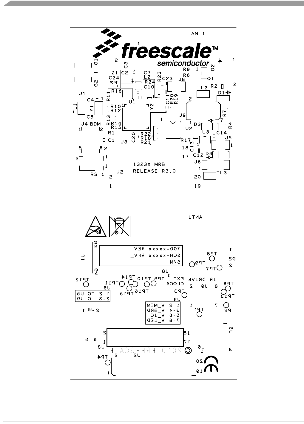
Figure 3-12. Modular Reference Board PCB Component Location (Top View)
Figure 3-13. Modular Reference Board PCB Test Points
1323x-Modular Reference Board
1323x Development Hardware Reference Manual, Rev. 1.0
Freescale Semiconductor 3-17
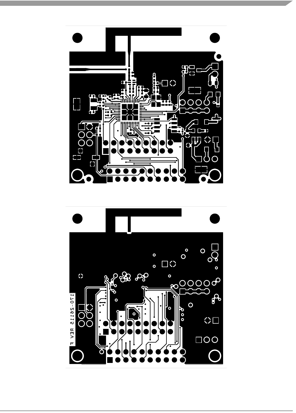
Figure 3-14. Modular Reference Board PCB Layout (Top View)
Figure 3-15. Modular Reference Board PCB Layout (Bottom View)

1323x-Modular Reference Board
1323x Development Hardware Reference Manual, Rev. 1.0
3-18 Freescale Semiconductor
3.4.1 Bill of Materials
Table 3-6. Bill of Materials
Item Qty Reference Value Description Mfg Name Mfg Part Number
1 1 ANT1 F_Antenna PCB F ANTENNA, NO PART
ORDER
Not A Part NOT A PART
2 4 BH1,BH2,BH3,
BH4
125 NON-PLATED MOUNTING
HOLE 125 DRILL / 160
KEEPOUT NO PART TO
ORDER
3 1 C1 1000pF CAP CER 1000PF 50V 5%
C0G 0402
Murata GRM1555C1H102JA01
D
4 3 C2,C17,C23
(No Not {Place)
10PF CAP CER 10PF 50V 5% C0G
0402
Murata GJM1555C1H100JB01
5 2 C3,C6 10PF CAP CER 10PF 50V 5% C0G
0402
Murata GJM1555C1H100JB01
6 4 C4,C5,C10,C1
1
12PF CAP CER 12PF 50V 5% C0G
0402
Murata GRM1555C1H120JZ01
D
7 1 C7 1PF CAP CER 1.0PF 50V
+/-0.25PF C0G 0402
Murata GJM1555C1H1R0CB01
D
8 4 C8,C9,C18,C2
2
0.22UF CAP CER 0.22UF 10V 10%
X5R 0402
Murata GRM155R61A224KE19
B
9 1 C12 1UF CAP CER 1.0UF 10V 10%
X7R 0603
Murata GRM188R71A105KA61
D
10 1 C13 2.2UF CAP CER 2.2UF 10V 10%
X7R 0603
Murata GRM188R71A225KE15
D
11 2 C14,C20 0.01UF CAP CER 0.01UF 50V 10%
X7R 0402
Murata GCM155R71H103KA55
D
12 1 C15 10UF CAP CER 10UF 10V 10% X5R
0805
Murata GRM21BR61A106KE19
_
13 1 C16 0.1UF CAP CER 0.1UF 16V 10%
X7R 0402
Tdk C1005X7R1C104KT
14 2 C25,C26 8.2PF CAP CER 8.2PF 50V 0.25PF
C0G 0402
Avx 04025A8R2CAT2A
15 1 D1 GREEN LED GRN SGL 30MA SMT
0805
Lite On LTST-C171KGKT
16 1 D2 VSLB3940 LED IR SGL 100MA RA TH Vishay
Intertechnology
VSLB3940
17 2 D3,D4 MBR0520LT1G DIODE SCH 0.5A 20V
SOD-123
On
Semiconductor
MBR0520LT1G
18 1 J1 SMA_EDGE CON 1 SKT SMA EDGE 34MIL
BOARD SMT 50 OHM -- 171H
AU 104L
Johnson
Components Inc
142-0701-881

1323x-Modular Reference Board
1323x Development Hardware Reference Manual, Rev. 1.0
Freescale Semiconductor 3-19
19 1 J2 HDR_10X2 HDR 2X10 TH 100MIL CTR
330H AU 100L
Samtec TSW-110-07-S-D
20 1 J3 HDR 2X9 HDR 2X9 TH 100MIL CTR
330H AU
Samtec TSW-109-07-S-D
21 1 J4 HDR 2X3 HDR 2X3 TH 100MIL CTR
335H AU 95L
Samtec TSW-103-07-S-D
22 2 J5,J8 HDR 1X2 HDR 1X2 TH 100MIL SP 330H
SN 115L
Samtec TSW-102-07-T-S
23 1 J6 HDR TH 1X3 HDR 1X3 TH 100MIL SP 339H
AU 100L
Samtec TSW-103-07-G-S
24 1 J9 HDR_2X4 HDR 2X4 TH 100MIL CTR
330H AU 100L
Samtec TSW-104-07-S-D
25 1 L1 0.0033UH IND -- 0.0027UH@100MHZ
300MA +/-0.3NH 0402
Murata LQG15HS2N7S02D
26 1 L2
(No Not {Place)
0.0039UH IND -- 0.0039UH@100MHZ
300MA +/-0.3NH 0402
Murata LQG15HN3N9S02D
27 1 Q1 MMBT3904LT1G TRAN NPN GEN 200MA 40V
SOT-23
On
Semiconductor
MMBT3904LT1G
28 1 RST1 SW_MOM SW SPST MOM PB 50MA 12V
SMT
Alps Electric
(Usa) Inc.
SKQYPDE010
29 1 R1 15K RES MF 15K 1/16W 5% 0402 Vishay
Intertechnology
CRCW040215K0JNED
30 1 R2 18.2 RES MF 18.2 OHM 1/4W 1%
0805
Rohm ESR10EZPF18R2
31 5 R4,R11,R13,R
25,R26
0 RES MF ZERO OHM 1/16W
5% 0402
Rohm MCR01MZPJ000
32 1 R6 1.5K RES MF 1.5K 1/16W 5% 0402 Vishay
Intertechnology
CRCW04021K50JNED
33 1 R7 330 RES MF 330 OHM 1/16W 5%
0402
Vishay
Intertechnology
CRCW0402330RJNED
34 1 R9 27K RES MF 27K 1/16W 5% 0402 Vishay
Intertechnology
CRCW040227K0JNED
35 2 R10,R12
(No Not {Place)
0 RES MF ZERO OHM 1/16W
5% 0402
Rohm MCR01MZPJ000
36 7 R14,R15,R16,
R17,R18,R21,
R22
10K RES MF 10K 1/16W 5% 0402 Vishay
Intertechnology
CRCW040210K0JNED
37 4 R19,R20,R23,
R24
(No Not {Place)
1K RES MF 1.0K 1/16W 5% 0402 Vishay
Intertechnology
CRCW04021K00JNED
38 3 TL1,TL2,TL3 TESTLOOP TEST POINT PAD SIZE
3.4MM X 1.8MM SMT
Keystone
Electronics
5015
Table 3-6. Bill of Materials
1323x-Modular Reference Board
1323x Development Hardware Reference Manual, Rev. 1.0
3-20 Freescale Semiconductor
39 16 TP1,TP2,TP3,T
P4,TP5,TP6,T
P7,TP8,TP9,T
P10,TP11,TP1
2,TP13,TP14,T
P15,TP16
TPAD_040 TEST POINT PAD 40MIL DIA
SMT, NO PART TO ORDER
Notacomponent NOTACOMPONENT
40 1 U1 MC1323X IC MCU+XCVR 8BITS 2.4GHZ
1.8-3.6V LGA48
Freescale
Semiconductor
PC13233C
41 1 U2 AT45DB021D IC MEM FLASH 256KX8
66MHz 2.7-3.6V 8S1
Atmel AT45DB021D-SSH-T
42 1 U3 LP2985AIM5-3.3 IC VREG LDO 3.3V 150MA
3.8-16V SOT-23-5
National
Semiconductor
LP2985AIM5-3.3/NOPB
43 1 Y1 32.768KHZ XTAL 32.768KHZ SMT ROHS
COMPLIANT
Epson
Electronics
FC-135 32.7680KA-A3
44 1 Y2 32MHZ XTAL 32MHZ 9PF -- SMT
3.2X2.5MM
Ndk EXS00A-CS02368
45 1 Z1 50/100 OHMS XFMR BALUN 2.45GHZ
+/-50MHZ 50/100OHM 3W
SMT
Johanson
Technology
2450BL15B100_
Table 3-6. Bill of Materials

1323x Development Hardware Reference Manual, Rev. 1.0
Freescale Semiconductor 4-1
Chapter 4
1323x Remote Control Motherboard
4.1 1323x-RCM Overview
The Remote Control Motherboard (1323x-RCM) is a motherboard that accepts the 1323x-Modular
Reference Board (1323x-MRB) plug-in module (daughter card) and supplies a power supply and a rich set
of interface peripherals. The two boards in combination provide a complete platform to evaluate the
MC1323x, write software, and develop a full featured IEEE 802.15.4 based wireless remote control.
4.1.1 Features
The 1323x-RCM provides the following features:
• 4-Layer metal, 0.034 inch thick FR4 board
• Two connectors provide daughter card mounting
— 20-Pin primary connector
— 18-Pin secondary connector
— Provide main supply voltage to board
— Provide access to all MC13233 GPIO
• Handheld battery operation
• Flexible power supply
— Sources include USB port, two AA batteries, or DC source
— Power-On green LED
—On-Off switch
• Used in conjunction with 1323x-MRB where MRB provides -
— 2.4 GHz IEEE 802.15.4 wireless node
— 2 Mbit serial FLASH for over-the-air programming (OTAP)
— IR blaster
• USB interface is bus-powered and full-speed compatible to the USB 2.0 and 1.1 specifications
• 36 Pushbutton 6x6 switch matrix
• 128x32 pixel monochrome graphic/alphanumeric LCD - uses SPI serial interface
• Synaptics® Touchpad™ - capacitive touch sensor
• 3-Axis accelerometer with IIC serial interface
• Four application-controlled blue indicator LEDs
• Single tone buzzer
1323x Remote Control Motherboard
1323x Development Hardware Reference Manual, Rev. 1.0
4-2 Freescale Semiconductor
4.1.2 Form Factor
Figure 4-1 shows a photo of the 1323x-RCM with the location of connectors and headers designated.
Figure 4-1. 1323x-RCM (1323x-MRB)
The1323x-Modular Reference Board (1323x-MRB) mounts on the 1323x-RCM via receptacles J8 and J9.
Figure 4-1 shows an outline of the 1323x-MRB placement when mounted.
Pushbutton
USB
Primary 20-Pin IO
Connector (J8)
On / Off
Secondary 18-Pin IO
Connector (J9)
128x32
Matrix
Connector
J15
Switch
SL1
1323x-MRB Outline
(When mounted)
4 Blue LEDs
External
Supply
J14
Accelerometer
Power-On
GPIO Enable
Pin Header
P1
GPIO Enable
Pin Header
P2
Graphic LCD
LED
Touchpad
Buzzer
(Mounted on
back side)
LCD J10
7.0 Inches
178 mm
3.4 Inches
86 mm
1323x Remote Control Motherboard
1323x Development Hardware Reference Manual, Rev. 1.0
Freescale Semiconductor 4-3
4.1.3 Board Level Specifications
NOTE
Temperature range specifications apply to RCM used in combination with
MRB.
Table 4-1. 1323x-RCM Specifications
Parameter Units Notes/Conditions
MIN TYP MAX
General
Size (PCB: X, Y) 86 x 178
3.40 x 7.00
mm
inches
Layer build (PCB) 0.8
0.034
mm
inches
4-Layer
Dielectric material (PCB) FR4
Power
Voltage supply (DC) 2.3 5 6 V
Voltage supply (USB) 4.4 5 5.25 V USB 2.0/1.1 standard specification
Voltage supply (Batteries) 2.8 3.2 V
Current consumption 100 mA
Temperature
Operating temperature; non-battery
operation (see note)
-20 +25 +70 °C Operating temperature is limited to +70 °C
due to switches. Basic circuit is good for a
maximum temperature of +85 °C.
Operating temperature; battery
operation (see note)
0 +25 +50 °C Operating temperature is limited by battery
temperature range
Storage temperature -30 +25 +70 °C
USB interface USB 2.0 and 1.1 full-speed compatible
Buzzer
CUI #CMI-1240 See data sheet
Touchpad
Synaptics Semi-custom
Tri-axis Low-g Accelerometer
MMA7660FC (Freescale Semi) See data sheet
LCD
CRYSTALFONZ
#CFAG12832A-YGH-N
See data sheet
Regulatory Approval
1323x Remote Control Motherboard
1323x Development Hardware Reference Manual, Rev. 1.0
4-4 Freescale Semiconductor
4.2 Functional Description
The 1323x-RCM is a host motherboard for the 1323x-MRB. The two-board combination provides a
powerful evaluation and development platform for the MC13233. Figure 4-2 shows a simple block
diagram. The 4-layer board provides a flexible power supply, 36 pushbutton matrix, 128x32 LCD,
Touchpad sensor, 3-axis accelerometer, four indicator LEDs, buzzer, and a USB <> UART serial port.
As the board name implies this platform is useful to develop an RF remote control application for a DTV,
entertainment console, or similar function. The 1323x-MRB provides the RF node and an IR transmitter
is available to support legacy IR protocol remote controls. The rich set of peripherals of the 1323x-RCM
allows a user to develop a remote control ranging from a simple input device to a higher end unit with
display.
In the following sections, refer to:
•Figure 4-1 for location of connectors and features
•Figure 4-2 for the functional blocks
•Figure 4-10 for the board schematic
CE (ETSI) Product is approved accordingly to the EN
300 328 V1.7.1 (2006-10) standard
CE (EMC) Product is approved accordingly to the EN
301 489-1 V1.6.1 (2005-09) and EN 301
489-17 V1.2.1 (2002-08) standards
Safety
UL Product is approved accordingly to the IEC
60950-1 and EN 60950-1, First Edition
standards
Environment
RoHS Product complies with the EU Directive
2002/95/EC of 27 January 2003
WEEE Product complies with the EU Directive
2002/95/EC of 27 January 2003
Table 4-1. 1323x-RCM Specifications (continued)
Parameter Units Notes/Conditions
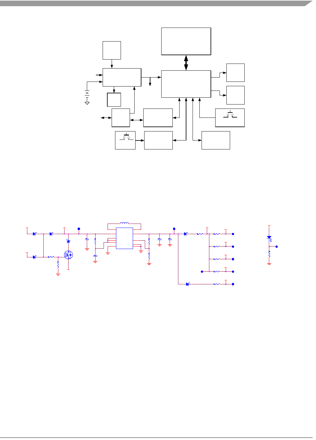
1323x Remote Control Motherboard
1323x Development Hardware Reference Manual, Rev. 1.0
Freescale Semiconductor 4-5
Figure 4-2. 1323x-RCM Block Diagram
4.2.1 Power Management
The 1323x-RCM can be powered from two AA batteries, the USB connector 5 V supply, or an external
DC supply and is also intended to power the 1323x-MRB. Figure 4-3 shows the power management
circuit.
Figure 4-3. 1323x-RCM Power Management Circuit
A boost-buck voltage regulator U8 is used in this design to allow operation over a relatively wide, low
voltage input range, i.e., the TPS63001 regulator has an input voltage range from 1.8 V to 5.5V. This
allows a broad range of power supply sources. The regulated output voltage of the TPS63001 is 3.3 V
which delivers about 3.05 V to the board due to the drop across the isolation Schottky diodes.
Attributes of the power management circuit include:
• Switch SL1 provides an ON/OFF function for all input voltage sources
• Red LED5 provides a POWER-ON indicator for all sources
• The 1323x-RCM can derive power from three different sources -
1. USB port Type-B connector J15 - power can be supplied from an actual USB port connection
or from an AC to DC converter that uses the USB connector to supply power.
1323x-MRB
GPIO Header
Receptacles
Buzzer
VCC
USB
2.0
4 Blue
Indicator
LEDs
USB
Type-B
Conn
On/Off
Switch
USB <> UART
Serial IC 6x6 Switch
Matrix
Power
Management GPIO
Pin Headers
On
LED
External DC
2 AA
Battery
Synaptic
Touchpad
IIC
128x32
Graphic/
Alphanumeric
LCD
SPI
2 PB
Switches
D13
MBR 0 520 LT 1G
V_BUZ
TP26R42
0
POWER ON
21
LED 5
RE D
V_LED
R39
330
V_MRB
V_ LED
V_DC
V_ TP D
BUZZER
V_ACC
C32
10UF EN
6
GN D
9
L1
4L2 2
PS/ SY NC
7
VOUT 1
VIN
5
VINA
8
FB 10
PGN D 3
PPAD 11
U8
T PS6 30 01
V_BAT
1 2
L3 3.3uH
1
32
Q3
S I 23 05
R38
4. 7 K
R41
10K
TP27
V_U SB VCC
TP 25
TP21
TP22
TP24
R45
0
C33
0.1UF
C43
10UF
R43
0
TP2 3
C42
10 U F
R35
0
R36
0
R37
0
R40
0
LED
TOUCHPAD
ACCELEROMETER
D8
MBR 0 52 0L T1 G
V_MA IN
R46
200K
DNP
MODULAR REFERENCE BOARD
R47
0
V_ 3V3
D9
MBR 0 52 0L T1 G
D10
MB R 05 20 LT 1G
TP1 9
D11
MBR0520LT1G
TP20
D12
MBR0520LT1G

1323x Remote Control Motherboard
1323x Development Hardware Reference Manual, Rev. 1.0
4-6 Freescale Semiconductor
2. External DC source via header J14 - a standard 0.1 in. spacing 1x2 pin header allows for
connection of an external DC supply.
3. Battery Operation - a battery holder that accommodates two AA batteries is mounted on the
non-component (back) side of the board and provides for battery operation.
– If either the USB or external DC source is present, the battery source is disabled by
MOSFET transistor Q3
– The sources are all isolated and protected by Schottky diodes
– The minimum effective battery operating voltage is controlled by the use the FTDI
FT232RQ USB <> UART device - leakage current back through the FT232RQ UART
connections to the MC13233 on the MRB can cause the Q3 MOSFET to partially turnoff at
battery voltage below approximately 2.7-2.8 Vdc.
NOTE
To avoid current leakage through the USB device and to have lowest
minimum battery operating voltage for battery-only operation, remove the
following jumpers:
• P1, Pins 7-8
• P1, Pins 11-12
• P1, Pins 17-18
• P1, Pins 21-22
NOTE
When battery operation is used, the temperature range of the two board
system should be limited to within the specified temperature range of the
battery technology. Table 4-1 limits temperature range from 0 °C to +50 °C
when battery operation is applied.
Table 4-2 lists the voltage source attributes.
.Table 4-2. 1323x-RCM Voltage Sources
Source Connector Input Voltage
Range Description
USB Port USB Type-B J15 4.4 V - 5.25 V • The input voltage range is set the USB Spec
• The voltage can be supplied by either a standard USB
cable connection or an AC to DC power adaptor that uses
the USB connector J15
• If a power adaptor is in use, the USB serial port cannot be
used