Freescale Semiconductor Mcf5480 Users Manual MCF5485 Reference
MCF5482 to the manual 710a7783-54b3-4687-a8c8-7060b4d7ef8c
2015-02-09
: Freescale-Semiconductor Freescale-Semiconductor-Mcf5480-Users-Manual-552182 freescale-semiconductor-mcf5480-users-manual-552182 freescale-semiconductor pdf
Open the PDF directly: View PDF ![]() .
.
Page Count: 1032 [warning: Documents this large are best viewed by clicking the View PDF Link!]
- MCF548x Reference Manual
- Table of Contents
- About This Book
- Chapter 1 Overview
- 1.1 MCF548x Family Overview
- 1.2 MCF548x Block Diagram
- 1.3 MCF548x Family Products
- 1.4 MCF548x Family Features
- 1.4.1 ColdFire V4e Core Overview
- 1.4.2 Debug Module (BDM)
- 1.4.3 JTAG
- 1.4.4 On-Chip Memories
- 1.4.5 PLL and Chip Clocking Options
- 1.4.6 Communications I/O Subsystem
- 1.4.7 DDR SDRAM Memory Controller
- 1.4.8 Peripheral Component Interconnect (PCI)
- 1.4.9 Flexible Local Bus (FlexBus)
- 1.4.10 Security Encryption Controller (SEC)
- 1.4.11 System Integration Unit (SIU)
- Chapter 2 Signal Descriptions
- 2.1 Introduction
- 2.2 MCF548x External Signals
- 2.2.1 FlexBus Signals
- 2.2.2 SDRAM Controller Signals
- 2.2.2.1 SDRAM Data Bus (SDDATA[31:0])
- 2.2.2.2 SDRAM Address Bus (SDADDR[12:0])
- 2.2.2.3 SDRAM Bank Addresses (SDBA[1:0])
- 2.2.2.4 SDRAM Row Address Strobe (RAS)
- 2.2.2.5 SDRAM Column Address Strobe (CAS)
- 2.2.2.6 SDRAM Chip Selects (SDCS[3:0])
- 2.2.2.7 SDRAM Write Data Byte Mask (SDDM[3:0])
- 2.2.2.8 SDRAM Data Strobe (SDDQS[3:0])
- 2.2.2.9 SDRAM Clock (SDCLK[1:0])
- 2.2.2.10 Inverted SDRAM Clock (SDCLK[1:0])
- 2.2.2.11 SDRAM Write Enable (SDWE)
- 2.2.2.12 SDRAM Clock Enable (SDCKE)
- 2.2.2.13 SDR SDRAM Data Strobe (SDRDQS)
- 2.2.2.14 SDRAM Reference Voltage (VREF)
- 2.2.3 PCI Controller Signals
- 2.2.3.1 PCI Address/Data Bus (PCIAD[31:0])
- 2.2.3.2 Command/Byte Enables (PCICXBE[3:0])
- 2.2.3.3 Device Select (PCIDEVSEL)
- 2.2.3.4 Frame (PCIFRM)
- 2.2.3.5 Initialization Device Select (PCIIDSEL)
- 2.2.3.6 Initiator Ready (PCIIRDY)
- 2.2.3.7 Parity (PCIPAR)
- 2.2.3.8 Parity Error (PCIPERR)
- 2.2.3.9 Reset (PCIRESET)
- 2.2.3.10 System Error (PCISERR)
- 2.2.3.11 Stop (PCISTOP)
- 2.2.3.12 Target Ready (PCITRDY)
- 2.2.3.13 External Bus Grant (PCIBG[4:1])
- 2.2.3.14 External Bus Grant/Request Output (PCIBG0/PCIREQOUT)
- 2.2.3.15 External Bus Request (PCIBR[4:0])
- 2.2.3.16 External Request/Grant Input (PCIBR0/PCIGNTIN)
- 2.2.4 Interrupt Control Signals
- 2.2.5 Clock and Reset Signals
- 2.2.6 Reset Configuration Pins
- 2.2.6.1 AD[12:8]-CLKIN to SDCLK Ratio (CLKCONFIG[4:0])
- 2.2.6.2 AD5-FlexBus Size Configuration (FBSIZE)
- 2.2.6.3 AD4-32-bit FlexBus Configuration (FBMODE)
- 2.2.6.4 AD3-Byte Enable Configuration (BECONFIG)
- 2.2.6.5 AD2-Auto Acknowledge Configuration (AACONFIG)
- 2.2.6.6 AD[1:0]-Port Size Configuration (PSCONFIG)
- 2.2.7 Ethernet Module Signals
- 2.2.7.1 Management Data (E0MDIO, E1MDIO)
- 2.2.7.2 Management Data Clock (E0MDC, E1MDC)
- 2.2.7.3 Transmit Clock (E0TXCLK, E1TXCLK)
- 2.2.7.4 Transmit Enable (E0TXEN, E1TXEN)
- 2.2.7.5 Transmit Data 0 (E0TXD0, E1TXD0)
- 2.2.7.6 Collision (E0COL, E1COL)
- 2.2.7.7 Receive Clock (E0RXCLK, E1RXCLK)
- 2.2.7.8 Receive Data Valid (E0RXDV, E1RXDV)
- 2.2.7.9 Receive Data 0 (E0RXD0, E1RXD0)
- 2.2.7.10 Carrier Receive Sense (E0CRS, E1CRS)
- 2.2.7.11 Transmit Data 1-3 (E0TXD[3:1], E1TXD[3:1])
- 2.2.7.12 Transmit Error (E0TXER, E1TXER)
- 2.2.7.13 Receive Data 1-3 (E0RXD[3:1], E1RXD[3:1])
- 2.2.7.14 Receive Error (E0RXER, E1RXER)
- 2.2.8 Universal Serial Bus (USB)
- 2.2.9 DMA Serial Peripheral Interface (DSPI) Signals
- 2.2.9.1 DSPI Synchronous Serial Data Output (DSPISOUT)
- 2.2.9.2 DSPI Synchronous Serial Data Input (DSPISIN)
- 2.2.9.3 DSPI Serial Clock (DSPISCK)
- 2.2.9.4 DSPI Peripheral Chip Select/Slave Select (DSPICS0/SS)
- 2.2.9.5 DSPI Chip Selects (DSPICS[2:3])
- 2.2.9.6 DSPI Peripheral Chip Select 5/Peripheral Chip Select Strobe (DSPICS5/PCSS)
- 2.2.10 FlexCAN Signals
- 2.2.11 I2C I/O Signals
- 2.2.12 PSC Module Signals
- 2.2.13 DMA Controller Module Signals
- 2.2.14 Timer Module Signals
- 2.2.15 Debug Support Signals
- 2.2.15.1 Processor Clock Output (PSTCLK)
- 2.2.15.2 Processor Status Debug Data (PSTDDATA[7:0])
- 2.2.15.3 Development Serial Clock/Test Reset (DSCLK/TRST)
- 2.2.15.4 Breakpoint/Test Mode Select (BKPT/TMS)
- 2.2.15.5 Development Serial Input/Test Data Input (DSI/TDI)
- 2.2.15.6 Development Serial Output/Test Data Output (DSO/TDO)
- 2.2.15.7 Test Clock (TCK)
- 2.2.16 Test Signals
- 2.2.17 Power and Reference Pins
- 2.2.17.1 Positive Pad Supply (EVDD)
- 2.2.17.2 Positive Core Supply (IVDD)
- 2.2.17.3 Ground (VSS)
- 2.2.17.4 USB Power (USBVDD)
- 2.2.17.5 USB Oscillator Power (USB_OSCVDD)
- 2.2.17.6 USB PHY Power (USB_PHYVDD)
- 2.2.17.7 USB Oscillator Analog Power (USB_OSCAVDD)
- 2.2.17.8 USB PLL Analog Power (USB_PLLVDD)
- 2.2.17.9 SDRAM Memory Supply (SDVDD)
- 2.2.17.10 PLL Analog Power (PLLVDD)
- 2.2.17.11 PLL Analog Ground (PLLVSS)
- Part I Processor Core
- Chapter 3 ColdFire Core
- 3.1 Core Overview
- 3.2 Features
- 3.3 Programming Model
- 3.4 Data Format Summary
- 3.5 Addressing Mode Summary
- 3.6 Instruction Set Summary
- 3.7 Instruction Execution Timing
- 3.8 Exception Processing Overview
- 3.9 Precise Faults
- Chapter 4 Enhanced Multiply-Accumulate Unit (EMAC)
- Chapter 5 Memory Management Unit (MMU)
- 5.1 Features
- 5.2 Virtual Memory Management Architecture
- 5.2.1 MMU Architecture Features
- 5.2.2 MMU Architecture Location
- 5.2.3 MMU Architecture Implementation
- 5.2.3.1 Precise Faults
- 5.2.3.2 MMU Access
- 5.2.3.3 Virtual Mode
- 5.2.3.4 Virtual Memory References
- 5.2.3.5 Instruction and Data Cache Addresses
- 5.2.3.6 Supervisor/User Stack Pointers
- 5.2.3.7 Access Error Stack Frame
- 5.2.3.8 Expanded Control Register Space
- 5.2.3.9 Changes to ACRs and CACR
- 5.2.3.10 ACR Address Improvements
- 5.2.3.11 Supervisor Protection
- 5.3 Debugging in a Virtual Environment
- 5.4 Virtual Memory Architecture Processor Support
- 5.5 MMU Definition
- 5.6 MMU Implementation
- 5.7 MMU Instructions
- Chapter 6 Floating-Point Unit (FPU)
- Chapter 7 Local Memory
- 7.1 Interactions between Local Memory Modules
- 7.2 SRAM Overview
- 7.3 SRAM Operation
- 7.4 SRAM Register Definition
- 7.5 SRAM Initialization
- 7.6 Power Management
- 7.7 Cache Overview
- 7.8 Cache Organization
- 7.9 Cache Operation
- 7.10 Cache Register Definition
- 7.11 Cache Management
- 7.12 Cache Operation Summary
- 7.13 Cache Initialization Code
- Chapter 8 Debug Support
- 8.1 Introduction
- 8.2 Signal Descriptions
- 8.3 Real-Time Trace Support
- 8.4 Memory Map/Register Definition
- 8.4.1 Revision A Shared Debug Resources
- 8.4.2 Configuration/Status Register (CSR)
- 8.4.3 PC Breakpoint ASID Control Register (PBAC)
- 8.4.4 BDM Address Attribute Register (BAAR)
- 8.4.5 Address Attribute Trigger Registers (AATR, AATR1)
- 8.4.6 Trigger Definition Register (TDR)
- 8.4.7 Program Counter Breakpoint and Mask Registers (PBRn, PBMR)
- 8.4.8 Address Breakpoint Registers (ABLR/ABLR1, ABHR/ABHR1)
- 8.4.9 Data Breakpoint and Mask Registers (DBR/DBR1, DBMR/DBMR1)
- 8.4.10 PC Breakpoint ASID Register (PBASID)
- 8.4.11 Extended Trigger Definition Register (XTDR)
- 8.5 Background Debug Mode (BDM)
- 8.5.1 CPU Halt
- 8.5.2 BDM Serial Interface
- 8.5.3 BDM Command Set
- 8.5.3.1 ColdFire BDM Command Format
- 8.5.3.2 Command Sequence Diagrams
- 8.5.3.3 Command Set Descriptions
- 8.5.3.3.1 Read A/D Register (rareg/rdreg)
- 8.5.3.3.2 Write A/D Register (wareg/wdreg)
- 8.5.3.3.3 Read Memory Location (read)
- 8.5.3.3.4 Write Memory Location (write)
- 8.5.3.3.5 Dump Memory Block (dump)
- 8.5.3.3.6 Fill Memory Block (fill)
- 8.5.3.3.7 Resume Execution (go)
- 8.5.3.3.8 No Operation (nop)
- 8.5.3.3.9 Synchronize PC to the PSTDDATA Lines (sync_pc)
- 8.5.3.3.10 Force Transfer Acknowledge (force_ta)
- 8.5.3.3.11 Read Control Register (rcreg)
- 8.5.3.3.12 BDM Accesses of the Stack Pointer Registers (A7: SSP and USP)
- 8.5.3.3.13 BDM Accesses of the EMAC Registers
- 8.5.3.3.14 BDM Accesses of Floating-Point Data Registers (FPn)
- 8.5.3.3.15 Write Control Register (wcreg)
- 8.5.3.3.16 Read Debug Module Register (rdmreg)
- 8.5.3.3.17 Write Debug Module Register (wdmreg)
- 8.6 Real-Time Debug Support
- 8.7 Debug C Definition of PSTDDATA Outputs
- 8.8 ColdFire Debug History
- 8.9 Freescale-Recommended BDM Pinout
- Chapter 3 ColdFire Core
- Part II System Integration Unit
- Chapter 9 System Integration Unit (SIU)
- Chapter 10 Internal Clocks and Bus Architecture
- 10.1 Introduction
- 10.2 PLL
- 10.3 XL Bus Arbiter
- 10.3.1 Features
- 10.3.2 Arbiter Functional Description
- 10.3.3 XLB Arbiter Register Descriptions
- 10.3.3.1 Arbiter Configuration Register (XARB_CFG)
- 10.3.3.2 Arbiter Version Register (XARB_VER)
- 10.3.3.3 Arbiter Status Register (XARB_SR)
- 10.3.3.4 Arbiter Interrupt Mask Register (XARB_IMR)
- 10.3.3.5 Arbiter Address Capture Register (XARB_ADRCAP)
- 10.3.3.6 Arbiter Bus Signal Capture Register (XARB_SIGCAP)
- 10.3.3.7 Arbiter Address Tenure Time Out Register (XARB_ADRTO)
- 10.3.3.8 Arbiter Data Tenure Time Out Register (XARB_DATTO)
- 10.3.3.9 Arbiter Bus Activity Time Out Register (XARB_BUSTO)
- 10.3.3.10 Arbiter Master Priority Enable Register (XARB_PRIEN)
- 10.3.3.11 Arbiter Master Priority Register (XARB_PRI)
- Chapter 11 General Purpose Timers (GPT)
- Chapter 12 Slice Timers (SLT)
- Chapter 13 Interrupt Controller
- 13.1 Introduction
- 13.2 Memory Map/Register Descriptions
- 13.2.1 Register Descriptions
- 13.2.1.1 Interrupt Pending Registers (IPRH, IPRL)
- 13.2.1.2 Interrupt Mask Register (IMRH, IMRL)
- 13.2.1.3 Interrupt Force Registers (INTFRCH, INTFRCL)
- 13.2.1.4 Interrupt Request Level Register (IRLR)
- 13.2.1.5 Interrupt Acknowledge Level and Priority Register (IACKLPR)
- 13.2.1.6 Interrupt Control Registers 1-63 (ICRn)
- 13.2.1.7 Software and Level n IACK Registers (SWIACKR, L1IACK-L7IACK)
- 13.2.1 Register Descriptions
- Chapter 14 Edge Port Module (EPORT)
- Chapter 15 GPIO
- 15.1 Introduction
- 15.2 External Pin Description
- 15.3 Memory Map/Register Definition
- 15.3.1 Register Overview
- 15.3.2 Register Descriptions
- 15.3.2.1 Port x Output Data Registers (PODR_x)
- 15.3.2.2 Port x Data Direction Registers (PDDR_x)
- 15.3.2.3 Port x Pin Data/Set Data Registers (PPDSDR_x)
- 15.3.2.4 Port x Clear Output Data Registers (PCLRR_x)
- 15.3.2.5 Port x Pin Assignment Registers (PAR_x)
- 15.3.2.6 FlexBus Chip Select Pin Assignment Register (PAR_FBCS)
- 15.3.2.7 DMA Pin Assignment Register (PAR_DMA)
- 15.3.2.8 FEC/I2C/IRQ Pin Assignment Register (PAR_FECI2CIRQ)
- 15.3.2.9 PCI Grant Pin Assignment Register (PAR_PCIBG)
- 15.3.2.10 PCI Request Pin Assignment Register (PAR_PCIBR)
- 15.3.2.11 PSC3 Pin Assignment Register (PAR_PSC3)
- 15.3.2.12 PSC2 Pin Assignment Register (PAR_PSC2)
- 15.3.2.13 PSC1 Pin Assignment Register (PAR_PSC1)
- 15.3.2.14 PSC0 Pin Assignment Register (PAR_PSC0)
- 15.3.2.15 DSPI Pin Assignment Register (PAR_DSPI)
- 15.3.2.16 General Purpose Timer Pin Assignment Register (PAR_TIMER)
- 15.4 Functional Description
- Part III On-Chip Integration
- Chapter 16 32-Kbyte System SRAM
- Chapter 17 FlexBus
- 17.1 Introduction
- 17.2 Byte Lanes
- 17.3 Address Latch
- 17.4 External Signals
- 17.5 Chip-Select Operation
- 17.6 Functional Description
- Chapter 18 SDRAM Controller (SDRAMC)
- 18.1 Introduction
- 18.2 Overview
- 18.3 External Signal Description
- 18.3.1 SDRAM Data Bus (SDDATA[31:0])
- 18.3.2 SDRAM Address Bus (SDADDR[12:0])
- 18.3.3 SDRAM Bank Addresses (SDBA[1:0])
- 18.3.4 SDRAM Row Address Strobe (RAS)
- 18.3.5 SDRAM Column Address Strobe (CAS)
- 18.3.6 SDRAM Chip Selects (SDCS[3:0])
- 18.3.7 SDRAM Write Data Byte Mask (SDDM[3:0])
- 18.3.8 SDRAM Data Strobe (SDDQS[3:0])
- 18.3.9 SDRAM Clock (SDCLK[1:0])
- 18.3.10 Inverted SDRAM Clock (SDCLK[1:0])
- 18.3.11 SDRAM Write Enable (SDWE)
- 18.3.12 SDRAM Clock Enable (SDCKE)
- 18.3.13 SDR SDRAM Data Strobe (SDRDQS)
- 18.3.14 SDRAM Memory Supply (SDVDD)
- 18.3.15 SDRAM Reference Voltage (VREF)
- 18.4 Interface Recommendations
- 18.5 SDRAM Overview
- 18.5.1 SDRAM Commands
- 18.5.2 Power-Up Initialization
- 18.6 Functional Overview
- 18.7 Memory Map/Register Definition
- 18.8 SDRAM Example
- 18.8.1 SDRAM Signal Drive Strength Settings
- 18.8.2 SDRAM Chip Select Settings
- 18.8.3 SDRAM Configuration 1 Register Settings
- 18.8.4 SDRAM Configuration 2 Register Settings
- 18.8.5 SDRAM Control Register Settings and PALL command
- 18.8.6 Set the Extended Mode Register
- 18.8.7 Set the Mode Register and Reset DLL
- 18.8.8 Issue a PALL command
- 18.8.9 Perform Two Refresh Cycles
- 18.8.10 Clear the Reset DLL Bit in the Mode Register
- 18.8.11 Enable Automatic Refresh and Lock Mode Register
- 18.8.12 Initialization Code
- Chapter 19 PCI Bus Controller
- 19.1 Introduction
- 19.2 External Signal Description
- 19.2.1 Address/Data Bus (PCIAD[31:0])
- 19.2.2 Command/Byte Enables (PCICXBE[3:0])
- 19.2.3 Device Select (PCIDEVSEL)
- 19.2.4 Frame (PCIFRAME)
- 19.2.5 Initialization Device Select (PCIIDSEL)
- 19.2.6 Initiator Ready (PCIIRDY)
- 19.2.7 Parity (PCIPAR)
- 19.2.8 PCI Clock (CLKIN)
- 19.2.9 Parity Error (PCIPERR)
- 19.2.10 Reset (PCIRESET)
- 19.2.11 System Error (PCISERR)
- 19.2.12 Stop (PCISTOP)
- 19.2.13 Target Ready (PCITRDY)
- 19.3 Memory Map/Register Definition
- 19.3.1 PCI Type 0 Configuration Registers
- 19.3.1.1 Device ID/Vendor ID Register (PCIIDR)-PCI Dword Addr 0
- 19.3.1.2 PCI Status/Command Register (PCISCR)-PCI Dword Addr 1
- 19.3.1.3 Revision ID/Class Code Register (PCICCRIR)-PCI Dword 3
- 19.3.1.4 Configuration 1 Register (PCICR1)-PCI Dword 3
- 19.3.1.5 Base Address Register 0 (PCIBAR0)-PCI Dword 4
- 19.3.1.6 Base Address Register 1 (PCIBAR1)-PCI Dword 5
- 19.3.1.7 CardBus CIS Pointer Register PCICCPR-PCI Dword A
- 19.3.1.8 Subsystem ID/Subsystem Vendor ID Registers PCISID-PCI Dword B
- 19.3.1.9 Expansion ROM Base Address PCIERBAR-PCI Dword C
- 19.3.1.10 Capabilities Pointer (Cap_Ptr) PCICPR-PCI Dword D
- 19.3.1.11 Configuration 2 Register (PCICR2)-PCI Dword F
- 19.3.2 General Control/Status Registers
- 19.3.2.1 Global Status/Control Register (PCIGSCR)
- 19.3.2.2 Target Base Address Translation Register 0 (PCITBATR0)
- 19.3.2.3 Target Base Address Translation Register 1 (PCITBATR1)
- 19.3.2.4 Target Control Register (PCITCR)
- 19.3.2.5 Initiator Window 0 Base/Translation Address Register (PCIIW0BTAR)
- 19.3.2.6 Initiator Window 1 Base/Translation Address Register (PCIIW1BTAR)
- 19.3.2.7 Initiator Window 2 Base/Translation Address Register (PCIIW2BTAR)
- 19.3.2.8 Initiator Window Configuration Register (PCIIWCR)
- 19.3.2.9 Initiator Control Register (PCIICR)
- 19.3.2.10 Initiator Status Register (PCIISR)
- 19.3.2.11 Configuration Address Register (PCICAR)
- 19.3.3 Communication Subsystem Interface Registers
- 19.3.3.1 Comm Bus FIFO Transmit Interface
- 19.3.3.1.1 Tx Packet Size Register (PCITPSR)
- 19.3.3.1.2 Tx Start Address Register (PCITSAR)
- 19.3.3.1.3 Tx Transaction Control Register (PCITTCR)
- 19.3.3.1.4 Tx Enables Register (PCITER)
- 19.3.3.1.5 Tx Next Address Register (PCITNAR)
- 19.3.3.1.6 Tx Last Word Register (PCITLWR)
- 19.3.3.1.7 Tx Done Counts Register (PCITDCR)
- 19.3.3.1.8 Tx Status Register (PCITSR)
- 19.3.3.1.9 Tx FIFO Data Register (PCITFDR)
- 19.3.3.1.10 Tx FIFO Status Register (PCITFSR)
- 19.3.3.1.11 Tx FIFO Control Register (PCITFCR)
- 19.3.3.1.12 Tx FIFO Alarm Register (PCITFAR)
- 19.3.3.1.13 Tx FIFO Read Pointer Register (PCITFRPR)
- 19.3.3.1.14 Tx FIFO Write Pointer Register (PCITFWPR)
- 19.3.3.2 Comm Bus FIFO Receive Interface
- 19.3.3.2.1 Rx Packet Size Register (PCIRPSR)
- 19.3.3.2.2 Rx Start Address Register (PCIRSAR)
- 19.3.3.2.3 Rx Transaction Control Register (PCIRTCR)
- 19.3.3.2.4 Rx Enables Register (PCIRER)
- 19.3.3.2.5 Rx Next Address Register (PCIRNAR)
- 19.3.3.2.6 Rx Done Counts Register (PCIRDCR)
- 19.3.3.2.7 Rx Status Register (PCIRSR)
- 19.3.3.2.8 Rx FIFO Data Register (PCIRFDR)
- 19.3.3.2.9 Rx FIFO Status Register (PCIRFSR)
- 19.3.3.2.10 Rx FIFO Control Register (PCIRFCR)
- 19.3.3.2.11 Rx FIFO Alarm Register (PCIRFAR)
- 19.3.3.2.12 Rx FIFO Read Pointer Register (PCIRFRPR)
- 19.3.3.2.13 Rx FIFO Write Pointer Register (PCIRFWPR)
- 19.3.3.1 Comm Bus FIFO Transmit Interface
- 19.3.1 PCI Type 0 Configuration Registers
- 19.4 Functional Description
- 19.5 Application Information
- 19.6 XL Bus Arbitration Priority
- Chapter 20 PCI Bus Arbiter Module
- Chapter 21 FlexCAN
- 21.1 Introduction
- 21.2 External Signals
- 21.3 Memory Map/Register Definition
- 21.3.1 FlexCAN Memory Map
- 21.3.2 Register Descriptions
- 21.3.2.1 FlexCAN Module Configuration Register (CANMCR)
- 21.3.2.2 FlexCAN Control Register (CANCTRL)
- 21.3.2.3 FlexCAN Timer Register (TIMER)
- 21.3.2.4 Rx Mask Registers
- 21.3.2.5 FlexCAN Error Counter Register (ERRCNT)
- 21.3.2.6 FlexCAN Error and Status Register (ERRSTAT)
- 21.3.2.7 Interrupt Mask Register (IMASK)
- 21.3.2.8 Interrupt Flag Register (IFLAG)
- 21.4 Functional Overview
- 21.5 FlexCAN Initialization Sequence
- Chapter 22 Integrated Security Engine (SEC)
- 22.1 Features
- 22.2 ColdFire Security Architecture
- 22.3 Block Diagram
- 22.4 Overview
- 22.5 Memory Map/Register Definition
- 22.6 Controller
- 22.6.1 EU Access
- 22.6.2 Multiple EU Assignment
- 22.6.3 Multiple Channels
- 22.6.4 Controller Registers
- 22.6.4.1 EU Assignment Control Registers (EUACRH and EUACRL)
- 22.6.4.2 EU Assignment Status Registers (EUASRH and EUASRL)
- 22.6.4.3 SEC Interrupt Mask Registers (SIMRH and SIMRL)
- 22.6.4.4 SEC Interrupt Status Registers (SISRH and SISRL)
- 22.6.4.5 SEC Interrupt Control Registers (SICRH and SICRL)
- 22.6.4.6 SEC ID Register (SIDR)
- 22.6.4.7 SEC Master Control Register (SMCR)
- 22.6.4.8 Master Error Address Register (MEAR)
- 22.7 Channels
- 22.8 ARC Four Execution Unit (AFEU)
- 22.9 Data Encryption Standard Execution Units (DEU)
- 22.10 Message Digest Execution Unit (MDEU)
- 22.11 RNG Execution Unit (RNG)
- 22.12 Advanced Encryption Standard Execution Units (AESU)
- 22.13 Descriptors
- 22.14 EU Specific Data Packet Descriptors
- Chapter 23 IEEE 1149.1 Test Access Port (JTAG)
- Part IV Communications Subsystem
- Chapter 24 Multichannel DMA
- 24.1 Introduction
- 24.2 External Signals
- 24.3 Memory Map/Register Definitions
- 24.3.1 DMA Task Memory
- 24.3.2 Memory Structure
- 24.3.3 DMA Registers
- 24.3.3.1 DMA Register Map
- 24.3.3.2 Task Base Address Register (TaskBAR)
- 24.3.3.3 Current Pointer (CP)
- 24.3.3.4 End Pointer (EP)
- 24.3.3.5 Variable Pointer (VP)
- 24.3.3.6 PTD Control (PTD)
- 24.3.3.7 DMA Interrupt Pending (DIPR)
- 24.3.3.8 DMA Interrupt Mask Register (DIMR)
- 24.3.3.9 Task Control Registers (TCRn)
- 24.3.3.10 Priority Registers (PRIORn)
- 24.3.3.11 Initiator Mux Control Register (IMCR)
- 24.3.3.12 Task Size Registers (TSKSZ[0:1])
- 24.3.3.13 Debug Comparator Registers (DBGCOMPn)
- 24.3.3.14 Debug Control (DBGCTL)
- 24.3.3.15 Debug Status (DBGSTAT)
- 24.3.3.16 PTD Debug Registers
- 24.3.4 External Request Module Registers
- 24.4 Functional Description
- 24.5 Programming Model
- 24.6 Timing Diagrams
- Chapter 25 Comm Timer Module (CTM)
- Chapter 26 Programmable Serial Controller (PSC)
- 26.1 Introduction
- 26.2 Signal Description
- 26.3 Memory Map/Register Definition
- 26.3.1 Overview
- 26.3.2 Module Memory Map
- 26.3.3 Register Descriptions
- 26.3.3.1 Mode Register 1(PSCMR1n)
- 26.3.3.2 Mode Register 2 (PSCMR2n)
- 26.3.3.3 Status Register (PSCSRn)
- 26.3.3.4 Clock Select Register (PSCCSRn)
- 26.3.3.5 Command Register (PSCCRn)
- 26.3.3.6 Receiver Buffer (PSCRBn) and Transmitter Buffer (PSCTBn)
- 26.3.3.7 Input Port Change Register (PSCIPCRn)
- 26.3.3.8 Auxiliary Control Register (PSCACRn)
- 26.3.3.9 Interrupt Status Register (PSCISRn)
- 26.3.3.10 Interrupt Mask Register (PSCIMRn)
- 26.3.3.11 Counter Timer Registers (PSCCTURn, PSCCTLRn)
- 26.3.3.12 Input Port (PSCIPn)
- 26.3.3.13 Output Port Bit Set (PSCOPSETn)
- 26.3.3.14 Output Port Bit Reset (PSCOPRESETn)
- 26.3.3.15 PSC/IrDA Control Register (PSCSICRn)
- 26.3.3.16 Infrared Control Register 1 (PSCIRCR1n)
- 26.3.3.17 Infrared Control Register 2 (PSCIRCR2n)
- 26.3.3.18 Infrared SIR Divide Register (PSCIRSDRn)
- 26.3.3.19 Infrared MIR Divide Register (PSCIRMDRn)
- 26.3.3.20 Infrared FIR Divide Register (PSCIRFDRn)
- 26.3.3.21 Rx and Tx FIFO Counter Register (PSCRFCNTn, PSCTFCNTn)
- 26.3.3.22 Rx and Tx FIFO Data Register (PSCRFDRn, PSCTFDRn)
- 26.3.3.23 Rx and Tx FIFO Status Register (PSCRFSRn, PSCTFSRn)
- 26.3.3.24 Rx and Tx FIFO Control Register (PSCRFCRn, PSCTFCRn)
- 26.3.3.25 Rx and Tx FIFO Alarm Register (PSCRFARn, PSCTFARn)
- 26.3.3.26 Rx and Tx FIFO Read Pointer (PSCRFRPn, PSCTFRPn)
- 26.3.3.27 Rx and Tx FIFO Write Pointer (PSCRFWPn, PSCTFWPn)
- 26.3.3.28 Rx and Tx FIFO Last Read Frame Pointer (PSCRLRFPn, PSCTLRFPn)
- 26.3.3.29 Rx and Tx FIFO Last Write Frame Pointer (PSCRLWFPn, PSCTLWFPn)
- 26.4 Functional Description
- 26.5 Resets
- 26.6 Interrupts
- 26.7 Software Environment
- Chapter 27 DMA Serial Peripheral Interface (DSPI)
- 27.1 Overview
- 27.2 Features
- 27.3 Block Diagram
- 27.4 Modes of Operation
- 27.5 Signal Description
- 27.5.1 Overview
- 27.5.2 Detailed Signal Descriptions
- 27.5.2.1 DSPI Peripheral Chip Select/Slave Select (DSPICS0/SS)
- 27.5.2.2 DSPI Peripheral Chip Selects 2-3 (DSPICS[2:3])
- 27.5.2.3 DSPI Peripheral Chip Select 5/Peripheral Chip Select Strobe (DSPICS5/PCSS)
- 27.5.2.4 DSPI Serial Input (DSPISIN)
- 27.5.2.5 DSPI Serial Output (DSPISOUT)
- 27.5.2.6 DSPI Serial Clock (DSPISCK)
- 27.6 Memory Map and Registers
- 27.6.1 DSPI Module Configuration Register (DMCR)
- 27.6.2 DSPI Transfer Count Register (DTCR)
- 27.6.3 DSPI Clock and Transfer Attributes Registers 0-7 (DCTARn)
- 27.6.4 DSPI Status Register (DSR)
- 27.6.5 DSPI DMA/Interrupt Request Select Register (DIRSR)
- 27.6.6 DSPI Tx FIFO Register (DTFR)
- 27.6.7 DSPI Rx FIFO Register (DRFR)
- 27.6.8 DSPI Tx FIFO Debug Registers 0-3 (DTFDRn)
- 27.6.9 DSPI Rx FIFO Debug Registers 0-3 (DRFDRn)
- 27.7 Functional Description
- 27.8 Initialization and Application Information
- Chapter 28 I2C Interface
- Chapter 29 USB 2.0 Device Controller
- 29.1 Introduction
- 29.2 Memory Map/Register Definition
- 29.2.1 USB Memory Map
- 29.2.2 USB Request, Control, and Status Registers
- 29.2.2.1 USB Status Register (USBSR)
- 29.2.2.2 USB Control Register (USBCR)
- 29.2.2.3 USB Descriptor RAM Control Register (DRAMCR)
- 29.2.2.4 USB Descriptor RAM Data Register (DRAMDR)
- 29.2.2.5 USB Interrupt Status Register (USBISR)
- 29.2.2.6 USB Interrupt Mask Register (USBIMR)
- 29.2.2.7 USB Application Interrupt Status Register (USBAISR)
- 29.2.2.8 USB Application Interrupt Mask Register (USBAIMR)
- 29.2.2.9 Endpoint Info Register (EPINFO)
- 29.2.2.10 USB Configuration Value Register (CFGR)
- 29.2.2.11 USB Configuration Attribute Register (CFGAR)
- 29.2.2.12 USB Device Speed Register (SPEEDR)
- 29.2.2.13 USB Frame Number Register (FRMNUMR)
- 29.2.2.14 USB Endpoint Transaction Number Register (EPTNR)
- 29.2.2.15 USB Application Interface Update Register (IFUR)
- 29.2.2.16 USB Configuration Interface Register (IFRn)
- 29.2.3 USB Counter Registers
- 29.2.3.1 USB Packet Passed Count Register (PPCNT)
- 29.2.3.2 USB Dropped Packet Counter Register (DPCNT)
- 29.2.3.3 USB CRC Error Counter Register (CRCECNT)
- 29.2.3.4 USB Bitstuffing Error Counter Register (BSECNT)
- 29.2.3.5 USB PID Error Counter Register (PIDECNT)
- 29.2.3.6 USB Framing Error Counter Register (FRMECNT)
- 29.2.3.7 USB Transmitted Packet Counter Register (TXPCNT)
- 29.2.3.8 USB Counter Overflow Register (CNTOVR)
- 29.2.4 Endpoint Context Registers
- 29.2.4.1 Endpoint n Attribute Control Register (EP0ACR, EPnOUTACR, EPnINACR)
- 29.2.4.2 Endpoint n Max Packet Size Register (EP0MPSR, EPnOUTMPSR, EPnINMPSR)
- 29.2.4.3 Endpoint n Interface Number Register (EP0IFR, EPnOUTIFR, EPnINIFR)
- 29.2.4.4 Endpoint n Status Register (EP0SR, EPnOUTSR, EPnINSR)
- 29.2.4.5 bmRequest Type Register (BMRTR)
- 29.2.4.6 bRequest Type Register (BRTR)
- 29.2.4.7 wValue Register (WVALUER)
- 29.2.4.8 wIndex Register (WINDEXR)
- 29.2.4.9 wLength Register (WLENGTHR)
- 29.2.4.10 Endpoint n Sync Frame Register (EPnOUTSFR, EPnINSFR)
- 29.2.5 USB Endpoint FIFO Registers
- 29.2.5.1 USB Endpoint n Status and Control Register (EPnSTAT)
- 29.2.5.2 USB Endpoint n Interrupt Status Register (EPnISR)
- 29.2.5.3 USB Endpoint n Interrupt Mask Register (EPnIMR)
- 29.2.5.4 USB Endpoint n FIFO RAM Configuration Register (EPnFRCFGR)
- 29.2.5.5 USB Endpoint n FIFO Data Register (EPnFDR)
- 29.2.5.6 USB Endpoint n FIFO Status Register (EPnFSR)
- 29.2.5.7 USB Endpoint n FIFO Control Register (EPnFCR)
- 29.2.5.8 USB Endpoint n FIFO Alarm Register (EPnFAR)
- 29.2.5.9 USB Endpoint n FIFO Read Pointer (EPnFRP)
- 29.2.5.10 USB Endpoint n FIFO Write Pointer (EPnFWP)
- 29.2.5.11 USB Endpoint n Last Read Frame Pointer (EPnLRFP)
- 29.2.5.12 USB Endpoint n Last Write Frame Pointer (EPnLWFP)
- 29.3 Functional Description
- 29.4 Software Interface
- Chapter 30 Fast Ethernet Controller (FEC)
- 30.1 Introduction
- 30.2 External Signals
- 30.2.1 Transmit Clock (EnTXCLK)
- 30.2.2 Receive Clock (EnRXCLK)
- 30.2.3 Transmit Enable (EnTXEN)
- 30.2.4 Transmit Data[3:0] (EnTXD[3:0])
- 30.2.5 Transmit Error (EnTXER)
- 30.2.6 Receive Data Valid (EnRXDV)
- 30.2.7 Receive Data[3:0] (EnRXD[3:0])
- 30.2.8 Receive Error (EnRXER)
- 30.2.9 Carrier Sense (EnCRS)
- 30.2.10 Collision (EnCOL)
- 30.2.11 Management Data Clock (EnMDC)
- 30.2.12 Management Data (EnMDIO)
- 30.3 Memory Map/Register Definition
- 30.3.1 Top Level Module Memory Map
- 30.3.2 Detailed Memory Map (Control/Status Registers)
- 30.3.3 MIB Block Counters Memory Map
- 30.3.3.1 Ethernet Interrupt Event Register (EIR)
- 30.3.3.2 Interrupt Mask Register (EIMR)
- 30.3.3.3 Ethernet Control Register (ECR)
- 30.3.3.4 MII Management Frame Register (MMFR)
- 30.3.3.5 MII Speed Control Register (MSCR)
- 30.3.3.6 MIB Control Register (MIBC)
- 30.3.3.7 Receive Control Register (RCR)
- 30.3.3.8 Receive Hash Register (RHR)
- 30.3.3.9 Transmit Control Register (TCR)
- 30.3.3.10 Physical Address Low Register (PALR)
- 30.3.3.11 Physical Address High Register (PAHR)
- 30.3.3.12 Opcode/Pause Duration Register (OPD)
- 30.3.3.13 Individual Address Upper Register (IAUR)
- 30.3.3.14 Individual Address Lower Register (IALR)
- 30.3.3.15 Group Address Upper Register (GAUR)
- 30.3.3.16 Group Address Lower Register (GALR)
- 30.3.3.17 FEC Transmit FIFO Watermark Register (FECTFWR)
- 30.3.3.18 FEC Receive FIFO Data Register (FECRFDR)
- 30.3.3.19 FEC Receive FIFO Status Register (FECRFSR)
- 30.3.3.20 FEC Receive FIFO Control Register (FECRFCR)
- 30.3.3.21 FEC Receive FIFO Last Read Frame Pointer Register (FECRLRFP)
- 30.3.3.22 FEC Receive FIFO Last Write Frame Pointer Register (FECRLWFP)
- 30.3.3.23 FEC Receive FIFO Alarm Register (FECRFAR)
- 30.3.3.24 FEC Receive FIFO Read Pointer Register (FECRFRP)
- 30.3.3.25 FEC Receive FIFO Write Pointer Register (FECRFWP)
- 30.3.3.26 FEC Transmit FIFO Data Register (FECTFDR)
- 30.3.3.27 FEC Transmit FIFO Status Register (FECTFSR)
- 30.3.3.28 FEC Transmit FIFO Control Register (FECTFCR)
- 30.3.3.29 FEC Transmit FIFO Last Read Frame Pointer Register (FECTLRFP)
- 30.3.3.30 FEC Transmit FIFO Last Write Frame Pointer Register (FECTLWFP)
- 30.3.3.31 FEC Transmit FIFO Alarm Register (FECTFAR)
- 30.3.3.32 FEC Transmit FIFO Read Pointer Register (FECTFRP)
- 30.3.3.33 FEC Transmit FIFO Write Pointer Register (FECTFWP)
- 30.3.3.34 FEC FIFO Reset Register (FECFRST)
- 30.3.3.35 FEC CRC and Transmit Frame Control Word Register (FECCTCWR)
- 30.4 Functional Description
- 30.4.1 Initialization Sequence
- 30.4.2 Frame Control/Status Words
- 30.4.3 Network Interface Options
- 30.4.4 FEC Frame Transmission
- 30.4.5 FEC Frame Reception
- 30.4.6 Ethernet Address Recognition
- 30.4.7 Hash Algorithm
- 30.4.8 Full Duplex Flow Control
- 30.4.9 Inter-Packet Gap (IPG) Time
- 30.4.10 Collision Handling
- 30.4.11 Internal and External Loopback
- 30.4.12 Ethernet Error-Handling Procedure
- 30.4.13 MII Data Frame
- 30.4.14 MII Management Frame Structure
- Chapter 24 Multichannel DMA
- Part V Mechanical
- Index

MCF548x Reference Manual
Devices Supported:
MCF5485 MCF5482
MCF5484 MCF5481
MCF5483 MCF5480
Document Number: MCF5485RM
Rev. 3
01/2006

How to Reach Us:
Home Page:
www.freescale.com
E-mail:
support@freescale.com
USA/Europe or Locations Not Listed:
Freescale Semiconductor
Technical Information Center, CH370
1300 N. Alma School Road
Chandler, Arizona 85224
+1-800-521-6274 or +1-480-768-2130
support@freescale.com
Europe, Middle East, and Africa:
Freescale Halbleiter Deutschland GmbH
Technical Information Center
Schatzbogen 7
81829 Muenchen, Germany
+44 1296 380 456 (English)
+46 8 52200080 (English)
+49 89 92103 559 (German)
+33 1 69 35 48 48 (French)
support@freescale.com
Japan:
Freescale Semiconductor Japan Ltd.
Headquarters
ARCO Tower 15F
1-8-1, Shimo-Meguro, Meguro-ku,
Tokyo 153-0064, Japan
0120 191014 or +81 3 5437 9125
support.japan@freescale.com
Asia/Pacific:
Freescale Semiconductor Hong Kong Ltd.
Technical Information Center
2 Dai King Street
Tai Po Industrial Estate
Tai Po, N.T., Hong Kong
+800 26668334
support.asia@freescale.com
For Literature Requests Only:
Freescale Semiconductor Literature Distribution Center
P.O. Box 5405
Denver, Colorado 80217
1-800-441-2447 or 303-675-2140
Fax: 303-675-2150
LDCForFreescaleSemiconductor@hibbertgroup.com
Information in this document is provided solely to enable system and
software implementers to use Freescale Semiconductor products. There are
no express or implied copyright licenses granted hereunder to design or
fabricate any integrated circuits or integrated circuits based on the
information in this document.
Freescale Semiconductor reserves the right to make changes without further
notice to any products herein. Freescale Semiconductor makes no warranty,
representation or guarantee regarding the suitability of its products for any
particular purpose, nor does Freescale Semiconductor assume any liability
arising out of the application or use of any product or circuit, and specifically
disclaims any and all liability, including without limitation consequential or
incidental damages. “Typical” parameters that may be provided in Freescale
Semiconductor data sheets and/or specifications can and do vary in different
applications and actual performance may vary over time. All operating
parameters, including “Typicals”, must be validated for each customer
application by customer’s technical experts. Freescale Semiconductor does
not convey any license under its patent rights nor the rights of others.
Freescale Semiconductor products are not designed, intended, or authorized
for use as components in systems intended for surgical implant into the body,
or other applications intended to support or sustain life, or for any other
application in which the failure of the Freescale Semiconductor product could
create a situation where personal injury or death may occur. Should Buyer
purchase or use Freescale Semiconductor products for any such unintended
or unauthorized application, Buyer shall indemnify and hold Freescale
Semiconductor and its officers, employees, subsidiaries, affiliates, and
distributors harmless against all claims, costs, damages, and expenses, and
reasonable attorney fees arising out of, directly or indirectly, any claim of
personal injury or death associated with such unintended or unauthorized
use, even if such claim alleges that Freescale Semiconductor was negligent
regarding the design or manufacture of the part.
Freescale™ and the Freescale logo are trademarks of Freescale
Semiconductor, Inc. All other product or service names are the property of their
respective owners.
© Freescale Semiconductor, Inc. 2006. All rights reserved.
MCF5485RM
Rev. 3
01/2006

Overview
Signal Descriptions
ColdFire Core
Enhanced Multiply-Accumulate Unit (EMAC)
Memory Management Unit (MMU)
Floating-Point Unit (FPU)
Debug Support
System Integration Unit (SIU)
Local Memory
Edge Port Module (EPORT)
Index
Interrupt Controller (INTC)
20
General Purpose I/O (GPIO)
14
13
15
PCI Bus Arbiter (PCIARB)
2
3
5
6
7
8
9
4
General Purpose Timers (GPT)
Slice Timers (SLT)
Internal Clocks and Bus Architecture 10
11
12
PCI Bus Controller (PCI) 19
FlexBus
SDRAM Controller (SDRAMC)
System SRAM 16
17
18
Integrated Secuity Engine (SEC)
FlexCAN
28
IEEE 1149.1 Test Access Port (JTAG)
22
21
23
DMA Serial Peripheral Interface (DSPI)
I2C interface 27
Comm Timer Module (CTM)
Programmable Serial Controller (PSC)
Multichannel DMA (MCD) 24
26
Mechanical Data
USB 2.0 Device Controller
Fast Ethernet Controller (FEC)
1
25
29
30
31
A
IND
Register Memory Map Quick Reference

Overview
Signal Descriptions
ColdFire Core
Enhanced Multiply-Accumulate Unit (EMAC)
Memory Management Unit (MMU)
Floating-Point Unit (FPU)
Debug Support
System Integration Unit (SIU)
Local Memory
Edge Port Module (EPORT)
Index
Interrupt Controller (INTC)
20
General Purpose I/O (GPIO)
14
13
15
PCI Bus Arbiter (PCIARB)
2
3
5
6
7
8
9
4
General Purpose Timers (GPT)
Slice Timers (SLT)
Internal Clocks and Bus Architecture
10
11
12
PCI Bus Controller (PCI)
19
FlexBus
SDRAM Controller (SDRAMC)
System SRAM
16
17
18
Integrated Secuity Engine (SEC)
FlexCAN
28
IEEE 1149.1 Test Access Port (JTAG)
22
21
23
DMA Serial Peripheral Interface (DSPI)
I2C interface
27
Comm Timer Module (CTM)
Programmable Serial Controller (PSC)
Multichannel DMA (MCD)
24
26
Mechanical Data
USB 2.0 Device Controller
Fast Ethernet Controller (FEC)
1
25
29
30
31
A
IND
Register Memory Map Quick Reference

MCF548x Reference Manual, Rev. 3
Freescale Semiconductor v
Contents
Paragraph
Number Title Page
Number
Chapter 1
Overview
1.1 MCF548x Family Overview ........................................................................................... 1-1
1.2 MCF548x Block Diagram .............................................................................................. 1-2
1.3 MCF548x Family Products ............................................................................................. 1-3
1.4 MCF548x Family Features ............................................................................................. 1-3
1.4.1 ColdFire V4e Core Overview ..................................................................................... 1-5
1.4.2 Debug Module (BDM) ................................................................................................ 1-6
1.4.3 JTAG ........................................................................................................................... 1-6
1.4.4 On-Chip Memories ..................................................................................................... 1-7
1.4.4.1 Caches ..................................................................................................................... 1-7
1.4.4.2 System SRAM ........................................................................................................ 1-7
1.4.5 PLL and Chip Clocking Options ................................................................................ 1-7
1.4.6 Communications I/O Subsystem ................................................................................ 1-8
1.4.6.1 DMA Controller ...................................................................................................... 1-8
1.4.6.2 10/100 Fast Ethernet Controller (FEC) ................................................................... 1-8
1.4.6.3 USB 2.0 Device (Universal Serial Bus) ................................................................. 1-8
1.4.6.4 Programmable Serial Controllers (PSCs) ............................................................... 1-9
1.4.6.5 I2C (Inter-Integrated Circuit) ................................................................................. 1-9
1.4.6.6 DMA Serial Peripheral Interface (DSPI) ................................................................ 1-9
1.4.6.7 Controller Area Network (CAN) .......................................................................... 1-10
1.4.7 DDR SDRAM Memory Controller ........................................................................... 1-10
1.4.8 Peripheral Component Interconnect (PCI) ............................................................... 1-10
1.4.9 Flexible Local Bus (FlexBus) ................................................................................... 1-10
1.4.10 Security Encryption Controller (SEC) ...................................................................... 1-11
1.4.11 System Integration Unit (SIU) .................................................................................. 1-11
1.4.11.1 Timers ................................................................................................................... 1-11
1.4.11.2 Interrupt Controller ............................................................................................... 1-12
1.4.11.3 General Purpose I/O ............................................................................................. 1-12
Chapter 2
Signal Descriptions
2.1 Introduction ..................................................................................................................... 2-1
2.1.1 Block Diagram ............................................................................................................ 2-1
2.2 MCF548x External Signals ........................................................................................... 2-16
2.2.1 FlexBus Signals ........................................................................................................ 2-16
2.2.1.1 Address/Data Bus (AD[31:0]) .............................................................................. 2-16
2.2.1.2 Chip Select (FBCS[5:0]) ....................................................................................... 2-17
2.2.1.3 Address Latch Enable (ALE) ................................................................................ 2-17

MCF548x Reference Manual, Rev. 3
vi Freescale Semiconductor
Contents
Paragraph
Number Title Page
Number
2.2.1.4 Read/Write (R/W) ................................................................................................. 2-17
2.2.1.5 Transfer Burst (TBST) .......................................................................................... 2-17
2.2.1.6 Transfer Size (TSIZ[1:0]) ..................................................................................... 2-17
2.2.1.7 Byte Selects (BE/BWE[3:0]) ................................................................................ 2-18
2.2.1.8 Output Enable (OE) .............................................................................................. 2-18
2.2.1.9 Transfer Acknowledge (TA) ................................................................................. 2-18
2.2.2 SDRAM Controller Signals ...................................................................................... 2-18
2.2.2.1 SDRAM Data Bus (SDDATA[31:0]) ................................................................... 2-18
2.2.2.2 SDRAM Address Bus (SDADDR[12:0]) ............................................................. 2-18
2.2.2.3 SDRAM Bank Addresses (SDBA[1:0]) ............................................................... 2-19
2.2.2.4 SDRAM Row Address Strobe (RAS) ................................................................... 2-19
2.2.2.5 SDRAM Column Address Strobe (CAS) ............................................................. 2-19
2.2.2.6 SDRAM Chip Selects (SDCS[3:0]) ...................................................................... 2-19
2.2.2.7 SDRAM Write Data Byte Mask (SDDM[3:0]) .................................................... 2-19
2.2.2.8 SDRAM Data Strobe (SDDQS[3:0]) .................................................................... 2-19
2.2.2.9 SDRAM Clock (SDCLK[1:0]) ............................................................................. 2-19
2.2.2.10 Inverted SDRAM Clock (SDCLK[1:0]) ............................................................... 2-19
2.2.2.11 SDRAM Write Enable (SDWE) ........................................................................... 2-19
2.2.2.12 SDRAM Clock Enable (SDCKE) ......................................................................... 2-19
2.2.2.13 SDR SDRAM Data Strobe (SDRDQS) ................................................................ 2-19
2.2.2.14 SDRAM Reference Voltage (VREF) ................................................................... 2-20
2.2.3 PCI Controller Signals .............................................................................................. 2-20
2.2.3.1 PCI Address/Data Bus (PCIAD[31:0]) ................................................................. 2-20
2.2.3.2 Command/Byte Enables (PCICXBE[3:0]) ........................................................... 2-20
2.2.3.3 Device Select (PCIDEVSEL) ............................................................................... 2-20
2.2.3.4 Frame (PCIFRM) .................................................................................................. 2-20
2.2.3.5 Initialization Device Select (PCIIDSEL) .............................................................. 2-20
2.2.3.6 Initiator Ready (PCIIRDY) ................................................................................... 2-20
2.2.3.7 Parity (PCIPAR) ................................................................................................... 2-20
2.2.3.8 Parity Error (PCIPERR) ....................................................................................... 2-20
2.2.3.9 Reset (PCIRESET) ............................................................................................... 2-21
2.2.3.10 System Error (PCISERR) ..................................................................................... 2-21
2.2.3.11 Stop (PCISTOP) ................................................................................................... 2-21
2.2.3.12 Target Ready (PCITRDY) .................................................................................... 2-21
2.2.3.13 External Bus Grant (PCIBG[4:1]) ........................................................................ 2-21
2.2.3.14 External Bus Grant/Request Output (PCIBG0/PCIREQOUT) ............................ 2-21
2.2.3.15 External Bus Request (PCIBR[4:0]) ..................................................................... 2-21
2.2.3.16 External Request/Grant Input (PCIBR0/PCIGNTIN) .......................................... 2-21
2.2.4 Interrupt Control Signals .......................................................................................... 2-21
2.2.4.1 Interrupt Request (IRQ[7:1]) ................................................................................ 2-21
2.2.5 Clock and Reset Signals ........................................................................................... 2-22

MCF548x Reference Manual, Rev. 3
Freescale Semiconductor vii
Contents
Paragraph
Number Title Page
Number
2.2.5.1 Reset In (RSTI) ..................................................................................................... 2-22
2.2.5.2 Reset Out (RSTO) ................................................................................................. 2-22
2.2.5.3 Clock In (CLKIN) ................................................................................................. 2-22
2.2.6 Reset Configuration Pins .......................................................................................... 2-22
2.2.6.1 AD[12:8]—CLKIN to SDCLK Ratio (CLKCONFIG[4:0]) ................................ 2-22
2.2.6.2 AD5—FlexBus Size Configuration (FBSIZE) ..................................................... 2-23
2.2.6.3 AD4—32-bit FlexBus Configuration (FBMODE) ............................................... 2-23
2.2.6.4 AD3—Byte Enable Configuration (BECONFIG) ................................................ 2-23
2.2.6.5 AD2—Auto Acknowledge Configuration (AACONFIG) .................................... 2-24
2.2.6.6 AD[1:0]—Port Size Configuration (PSCONFIG) ................................................ 2-24
2.2.7 Ethernet Module Signals ........................................................................................... 2-24
2.2.7.1 Management Data (E0MDIO, E1MDIO) ............................................................. 2-24
2.2.7.2 Management Data Clock (E0MDC, E1MDC) ...................................................... 2-25
2.2.7.3 Transmit Clock (E0TXCLK, E1TXCLK) ............................................................ 2-25
2.2.7.4 Transmit Enable (E0TXEN, E1TXEN) ................................................................ 2-25
2.2.7.5 Transmit Data 0 (E0TXD0, E1TXD0) ................................................................. 2-25
2.2.7.6 Collision (E0COL, E1COL) ................................................................................. 2-25
2.2.7.7 Receive Clock (E0RXCLK, E1RXCLK) ............................................................. 2-25
2.2.7.8 Receive Data Valid (E0RXDV, E1RXDV) .......................................................... 2-25
2.2.7.9 Receive Data 0 (E0RXD0, E1RXD0) .................................................................. 2-25
2.2.7.10 Carrier Receive Sense (E0CRS, E1CRS) ............................................................. 2-25
2.2.7.11 Transmit Data 1–3 (E0TXD[3:1], E1TXD[3:1]) .................................................. 2-25
2.2.7.12 Transmit Error (E0TXER, E1TXER) ................................................................... 2-26
2.2.7.13 Receive Data 1–3 (E0RXD[3:1], E1RXD[3:1]) ................................................... 2-26
2.2.7.14 Receive Error (E0RXER, E1RXER) .................................................................... 2-26
2.2.8 Universal Serial Bus (USB) ...................................................................................... 2-26
2.2.8.1 USB Differential Data (USBD+, USBD–) ........................................................... 2-26
2.2.8.2 USBVBUS ............................................................................................................ 2-26
2.2.8.3 USBRBIAS ........................................................................................................... 2-26
2.2.8.4 USBCLKIN .......................................................................................................... 2-26
2.2.8.5 USBCLKOUT ...................................................................................................... 2-26
2.2.9 DMA Serial Peripheral Interface (DSPI) Signals ..................................................... 2-26
2.2.9.1 DSPI Synchronous Serial Data Output (DSPISOUT) .......................................... 2-26
2.2.9.2 DSPI Synchronous Serial Data Input (DSPISIN) ................................................. 2-27
2.2.9.3 DSPI Serial Clock (DSPISCK) ............................................................................. 2-27
2.2.9.4 DSPI Peripheral Chip Select/Slave Select (DSPICS0/SS) ................................... 2-27
2.2.9.5 DSPI Chip Selects (DSPICS[2:3]) ........................................................................ 2-27
2.2.9.6 DSPI Peripheral Chip Select 5/Peripheral Chip Select Strobe (DSPICS5/PCSS) 2-27
2.2.10 FlexCAN Signals ...................................................................................................... 2-27
2.2.10.1 FlexCAN Transmit (CANTX0, CANTX1) .......................................................... 2-27
2.2.10.2 FlexCAN Receive (CANRX0, CANRX1) ........................................................... 2-27

MCF548x Reference Manual, Rev. 3
viii Freescale Semiconductor
Contents
Paragraph
Number Title Page
Number
2.2.11 I2C I/O Signals .......................................................................................................... 2-27
2.2.11.1 Serial Clock (SCL) ............................................................................................... 2-28
2.2.11.2 Serial Data (SDA) ................................................................................................. 2-28
2.2.12 PSC Module Signals ................................................................................................. 2-28
2.2.12.1 Transmit Serial Data Output (PSC0TXD, PSC1TXD, PSC2TXD, PSC3TXD) .. 2-28
2.2.12.2 Receive Serial Data Input (PSC0RXD, PSC1RXD, PSC2RXD, PSC3RXD) ..... 2-28
2.2.12.3 Clear-to-Send (PSCnCTS/PSCBCLK) ................................................................. 2-28
2.2.12.4 Request-to-Send (PSCnRTS/PSCFSYNC) ........................................................... 2-28
2.2.13 DMA Controller Module Signals ............................................................................. 2-28
2.2.13.1 DMA Request (DREQ[1:0]) ................................................................................. 2-28
2.2.13.2 DMA Acknowledge (DACK[1:0]) ....................................................................... 2-28
2.2.14 Timer Module Signals .............................................................................................. 2-29
2.2.14.1 Timer Inputs (TIN[3:0]) ....................................................................................... 2-29
2.2.14.2 Timer Outputs (TOUT[3:0]) ................................................................................. 2-29
2.2.15 Debug Support Signals ............................................................................................. 2-29
2.2.15.1 Processor Clock Output (PSTCLK) ...................................................................... 2-29
2.2.15.2 Processor Status Debug Data (PSTDDATA[7:0]) ............................................... 2-29
2.2.15.3 Development Serial Clock/Test Reset (DSCLK/TRST) ...................................... 2-29
2.2.15.4 Breakpoint/Test Mode Select (BKPT/TMS) ........................................................ 2-30
2.2.15.5 Development Serial Input/Test Data Input (DSI/TDI) ......................................... 2-30
2.2.15.6 Development Serial Output/Test Data Output (DSO/TDO) ................................. 2-30
2.2.15.7 Test Clock (TCK) ................................................................................................. 2-30
2.2.16 Test Signals ............................................................................................................... 2-30
2.2.16.1 Test Mode (MTMOD[3:0]) .................................................................................. 2-30
2.2.17 Power and Reference Pins ........................................................................................ 2-31
2.2.17.1 Positive Pad Supply (EVDD) ............................................................................... 2-31
2.2.17.2 Positive Core Supply (IVDD) ............................................................................... 2-31
2.2.17.3 Ground (VSS) ....................................................................................................... 2-31
2.2.17.4 USB Power (USBVDD) ....................................................................................... 2-31
2.2.17.5 USB Oscillator Power (USB_OSCVDD) ............................................................. 2-31
2.2.17.6 USB PHY Power (USB_PHYVDD) .................................................................... 2-31
2.2.17.7 USB Oscillator Analog Power (USB_OSCAVDD) ............................................. 2-31
2.2.17.8 USB PLL Analog Power (USB_PLLVDD) ......................................................... 2-31
2.2.17.9 SDRAM Memory Supply (SDVDD) .................................................................... 2-31
2.2.17.10 PLL Analog Power (PLLVDD) ............................................................................ 2-31
2.2.17.11 PLL Analog Ground (PLLVSS) ........................................................................... 2-31

MCF548x Reference Manual, Rev. 3
Freescale Semiconductor ix
Contents
Paragraph
Number Title Page
Number
Chapter 3
ColdFire Core
3.1 Core Overview ................................................................................................................ 3-1
3.2 Features ........................................................................................................................... 3-1
3.2.1 Enhanced Pipelines ..................................................................................................... 3-2
3.2.1.1 Instruction Fetch Pipeline (IFP) .............................................................................. 3-3
3.2.1.2 Operand Execution Pipeline (OEP) ........................................................................ 3-4
3.2.1.3 Harvard Memory Architecture ............................................................................... 3-6
3.2.2 Debug Module Enhancements .................................................................................... 3-6
3.3 Programming Model ....................................................................................................... 3-7
3.3.1 User Programming Model .......................................................................................... 3-9
3.3.1.1 Data Registers (D0–D7) ......................................................................................... 3-9
3.3.1.2 Address Registers (A0–A6) .................................................................................... 3-9
3.3.2 User Stack Pointer (A7) ............................................................................................. 3-9
3.3.2.1 Program Counter (PC) ............................................................................................ 3-9
3.3.2.2 Condition Code Register (CCR) ............................................................................. 3-9
3.3.3 EMAC Programming Model .................................................................................... 3-10
3.3.4 FPU Programming Model ......................................................................................... 3-10
3.3.5 Supervisor Programming Model ............................................................................... 3-11
3.3.5.1 Status Register (SR) .............................................................................................. 3-12
3.3.5.2 Vector Base Register (VBR) ................................................................................ 3-12
3.3.5.3 Cache Control Register (CACR) .......................................................................... 3-13
3.3.5.4 Access Control Registers (ACR0–ACR3) ............................................................ 3-13
3.3.5.5 RAM Base Address Registers (RAMBAR0 and RAMBAR1) ............................ 3-13
3.3.5.6 Module Base Address Register (MBAR) ............................................................. 3-13
3.3.6 Programming Model Table ....................................................................................... 3-13
3.4 Data Format Summary .................................................................................................. 3-15
3.4.1 Data Organization in Registers ................................................................................. 3-15
3.4.1.1 Integer Data Format Organization in Registers .................................................... 3-15
3.4.1.2 Integer Data Format Organization in Memory ..................................................... 3-16
3.4.2 EMAC Data Representation ..................................................................................... 3-17
3.4.2.1 Floating-Point Data Formats and Types ............................................................... 3-17
3.5 Addressing Mode Summary ......................................................................................... 3-18
3.6 Instruction Set Summary .............................................................................................. 3-19
3.6.1 Additions to the Instruction Set Architecture ........................................................... 3-19
3.6.2 Instruction Set Summary .......................................................................................... 3-22
3.7 Instruction Execution Timing ....................................................................................... 3-27
3.7.1 MOVE Instruction Execution Timing ...................................................................... 3-28
3.7.2 One-Operand Instruction Execution Timing ............................................................ 3-30
3.7.3 Two-Operand Instruction Execution Timing ............................................................ 3-31

MCF548x Reference Manual, Rev. 3
xFreescale Semiconductor
Contents
Paragraph
Number Title Page
Number
3.7.4 Miscellaneous Instruction Execution Timing ........................................................... 3-32
3.7.5 Branch Instruction Execution Timing ....................................................................... 3-33
3.7.6 EMAC Instruction Execution Times ........................................................................ 3-34
3.7.7 FPU Instruction Execution Times ............................................................................. 3-35
3.8 Exception Processing Overview ................................................................................... 3-36
3.8.1 Exception Stack Frame Definition ............................................................................ 3-38
3.8.2 Processor Exceptions ................................................................................................ 3-39
3.9 Precise Faults ................................................................................................................ 3-42
Chapter 4
Enhanced Multiply-Accumulate Unit (EMAC)
4.1 Introduction ..................................................................................................................... 4-1
4.1.1 MAC Overview ........................................................................................................... 4-2
4.1.2 General Operation ....................................................................................................... 4-2
4.2 Memory Map/Register Definition .................................................................................. 4-5
4.2.1 MAC Status Register (MACSR) ................................................................................. 4-5
4.2.1.1 Fractional Operation Mode ..................................................................................... 4-8
4.2.2 Mask Register (MASK) ............................................................................................ 4-10
4.3 EMAC Instruction Set Summary .................................................................................. 4-11
4.3.1 EMAC Instruction Execution Timing ....................................................................... 4-11
4.3.2 Data Representation .................................................................................................. 4-12
4.3.3 EMAC Opcodes ........................................................................................................ 4-13
Chapter 5
Memory Management Unit (MMU)
5.1 Features ........................................................................................................................... 5-1
5.2 Virtual Memory Management Architecture ................................................................... 5-1
5.2.1 MMU Architecture Features ....................................................................................... 5-1
5.2.2 MMU Architecture Location ...................................................................................... 5-2
5.2.3 MMU Architecture Implementation ........................................................................... 5-3
5.2.3.1 Precise Faults ..........................................................................................................5-4
5.2.3.2 MMU Access .......................................................................................................... 5-4
5.2.3.3 Virtual Mode ........................................................................................................... 5-4
5.2.3.4 Virtual Memory References ................................................................................... 5-4
5.2.3.5 Instruction and Data Cache Addresses ................................................................... 5-4
5.2.3.6 Supervisor/User Stack Pointers .............................................................................. 5-5
5.2.3.7 Access Error Stack Frame ...................................................................................... 5-5
5.2.3.8 Expanded Control Register Space .......................................................................... 5-5

MCF548x Reference Manual, Rev. 3
Freescale Semiconductor xi
Contents
Paragraph
Number Title Page
Number
5.2.3.9 Changes to ACRs and CACR ................................................................................. 5-5
5.2.3.10 ACR Address Improvements .................................................................................. 5-6
5.2.3.11 Supervisor Protection .............................................................................................. 5-7
5.3 Debugging in a Virtual Environment .............................................................................. 5-7
5.4 Virtual Memory Architecture Processor Support ........................................................... 5-7
5.4.1 Precise Faults .............................................................................................................. 5-7
5.4.2 Supervisor/User Stack Pointers ................................................................................. 5-7
5.4.3 Access Error Stack Frame Additions .......................................................................... 5-8
5.5 MMU Definition ............................................................................................................. 5-9
5.5.1 Effective Address Attribute Determination ................................................................ 5-9
5.5.2 MMU Functionality .................................................................................................. 5-10
5.5.3 MMU Organization ................................................................................................... 5-10
5.5.3.1 MMU Base Address Register (MMUBAR) ......................................................... 5-10
5.5.3.2 MMU Memory Map ............................................................................................. 5-11
5.5.3.3 MMU Control Register (MMUCR) ..................................................................... 5-11
5.5.3.4 MMU Operation Register (MMUOR) .................................................................. 5-12
5.5.3.5 MMU Status Register (MMUSR) ......................................................................... 5-14
5.5.3.6 MMU Fault, Test, or TLB Address Register (MMUAR) ..................................... 5-15
5.5.3.7 MMU Read/Write Tag and Data Entry Registers (MMUTR and MMUDR) ...... 5-16
5.5.4 MMU TLB ................................................................................................................ 5-18
5.5.5 MMU Operation ....................................................................................................... 5-19
5.6 MMU Implementation .................................................................................................. 5-20
5.6.1 TLB Address Fields .................................................................................................. 5-20
5.6.2 TLB Replacement Algorithm ................................................................................... 5-21
5.6.3 TLB Locked Entries .................................................................................................. 5-22
5.7 MMU Instructions ......................................................................................................... 5-23
Chapter 6
Floating-Point Unit (FPU)
6.1 Introduction ..................................................................................................................... 6-1
6.1.1 Overview ..................................................................................................................... 6-1
6.1.1.1 Notational Conventions .......................................................................................... 6-1
6.2 Operand Data Formats and Types .................................................................................. 6-3
6.2.1 Signed-Integer Data Formats ...................................................................................... 6-3
6.2.2 Floating-Point Data Formats ....................................................................................... 6-3
6.2.3 Floating-Point Data Types .......................................................................................... 6-4
6.2.3.1 Normalized Numbers .............................................................................................. 6-4
6.2.3.2 Zeros ....................................................................................................................... 6-4
6.2.3.3 Infinities .................................................................................................................. 6-4
6.2.3.4 Not-A-Number ........................................................................................................ 6-5

MCF548x Reference Manual, Rev. 3
xii Freescale Semiconductor
Contents
Paragraph
Number Title Page
Number
6.2.3.5 Denormalized Numbers .......................................................................................... 6-5
6.3 Register Definition .......................................................................................................... 6-7
6.3.1 Floating-Point Data Registers (FP0–FP7) .................................................................. 6-7
6.3.2 Floating-Point Control Register (FPCR) .................................................................... 6-7
6.3.3 Floating-Point Status Register (FPSR) ....................................................................... 6-9
6.3.4 Floating-Point Instruction Address Register (FPIAR) .............................................. 6-10
6.4 Floating-Point Computational Accuracy ...................................................................... 6-11
6.4.1 Intermediate Result ................................................................................................... 6-11
6.4.2 Rounding the Result .................................................................................................. 6-12
6.5 Floating-Point Post-Processing ..................................................................................... 6-14
6.5.1 Underflow, Round, and Overflow ............................................................................ 6-14
6.5.2 Conditional Testing ................................................................................................... 6-15
6.6 Floating-Point Exceptions ............................................................................................. 6-17
6.6.1 Floating-Point Arithmetic Exceptions ...................................................................... 6-18
6.6.1.1 Branch/Set on Unordered (BSUN) ....................................................................... 6-19
6.6.1.2 Input Not-A-Number (INAN) ............................................................................... 6-20
6.6.1.3 Input Denormalized Number (IDE) ...................................................................... 6-20
6.6.1.4 Operand Error (OPERR) ....................................................................................... 6-21
6.6.1.5 Overflow (OVFL) ................................................................................................. 6-21
6.6.1.6 Underflow (UNFL) ............................................................................................... 6-22
6.6.1.7 Divide-by-Zero (DZ) ............................................................................................ 6-22
6.6.1.8 Inexact Result (INEX) .......................................................................................... 6-23
6.6.2 Floating-Point State Frames ...................................................................................... 6-23
6.7 Instructions .................................................................................................................... 6-25
6.7.1 Floating-Point Instruction Overview ........................................................................ 6-25
6.7.2 Floating-Point Instruction Execution Timing ........................................................... 6-27
6.7.3 Key Differences between ColdFire and M68000 FPU Programming Models ......... 6-28
Chapter 7
Local Memory
7.1 Interactions between Local Memory Modules ............................................................... 7-1
7.2 SRAM Overview ............................................................................................................ 7-1
7.3 SRAM Operation ............................................................................................................ 7-2
7.4 SRAM Register Definition ............................................................................................. 7-2
7.4.1 SRAM Base Address Registers (RAMBAR0/RAMBAR1) ....................................... 7-2
7.5 SRAM Initialization ........................................................................................................ 7-4
7.5.1 SRAM Initialization Code .......................................................................................... 7-5
7.6 Power Management ........................................................................................................ 7-6
7.7 Cache Overview ..............................................................................................................7-6
7.8 Cache Organization ......................................................................................................... 7-7

MCF548x Reference Manual, Rev. 3
Freescale Semiconductor xiii
Contents
Paragraph
Number Title Page
Number
7.8.1 Cache Line States: Invalid, Valid-Unmodified, and Valid-Modified ......................... 7-8
7.8.2 The Cache at Start-Up ................................................................................................. 7-8
7.9 Cache Operation ........................................................................................................... 7-10
7.9.1 Caching Modes ......................................................................................................... 7-12
7.9.1.1 Cacheable Accesses .............................................................................................. 7-12
7.9.1.2 Cache-Inhibited Accesses ..................................................................................... 7-13
7.9.2 Cache Protocol .......................................................................................................... 7-14
7.9.2.1 Read Miss ............................................................................................................. 7-14
7.9.2.2 Write Miss (Data Cache Only) ............................................................................. 7-14
7.9.2.3 Read Hit ................................................................................................................7-15
7.9.2.4 Write Hit (Data Cache Only) ................................................................................ 7-15
7.9.3 Cache Coherency (Data Cache Only) ....................................................................... 7-15
7.9.4 Memory Accesses for Cache Maintenance ............................................................... 7-15
7.9.4.1 Cache Filling ......................................................................................................... 7-15
7.9.4.2 Cache Pushes ........................................................................................................ 7-16
7.9.5 Cache Locking .......................................................................................................... 7-17
7.10 Cache Register Definition ............................................................................................. 7-19
7.10.1 Cache Control Register (CACR) .............................................................................. 7-19
7.10.2 Access Control Registers (ACR0–ACR3) ................................................................ 7-22
7.11 Cache Management ....................................................................................................... 7-23
7.12 Cache Operation Summary ........................................................................................... 7-26
7.12.1 Instruction Cache State Transitions .......................................................................... 7-26
7.12.2 Data Cache State Transitions .................................................................................... 7-27
7.13 Cache Initialization Code .............................................................................................. 7-30
Chapter 8
Debug Support
8.1 Introduction ..................................................................................................................... 8-1
8.1.1 Overview ..................................................................................................................... 8-1
8.2 Signal Descriptions .........................................................................................................8-2
8.2.1 Processor Status/Debug Data (PSTDDATA[7:0]) ..................................................... 8-3
8.3 Real-Time Trace Support ................................................................................................ 8-5
8.3.1 Begin Execution of Taken Branch (PST = 0x5) ......................................................... 8-6
8.3.2 Processor Stopped or Breakpoint State Change (PST = 0xE) .................................... 8-7
8.3.3 Processor Halted (PST = 0xF) .................................................................................... 8-8
8.4 Memory Map/Register Definition .................................................................................. 8-9
8.4.1 Revision A Shared Debug Resources ....................................................................... 8-11
8.4.2 Configuration/Status Register (CSR) ........................................................................ 8-11
8.4.3 PC Breakpoint ASID Control Register (PBAC) ....................................................... 8-14
8.4.4 BDM Address Attribute Register (BAAR) ............................................................... 8-15

MCF548x Reference Manual, Rev. 3
xiv Freescale Semiconductor
Contents
Paragraph
Number Title Page
Number
8.4.5 Address Attribute Trigger Registers (AATR, AATR1) ............................................ 8-16
8.4.6 Trigger Definition Register (TDR) ........................................................................... 8-17
8.4.7 Program Counter Breakpoint and Mask Registers (PBRn, PBMR) ......................... 8-20
8.4.8 Address Breakpoint Registers (ABLR/ABLR1, ABHR/ABHR1) ........................... 8-21
8.4.9 Data Breakpoint and Mask Registers (DBR/DBR1, DBMR/DBMR1) .................... 8-22
8.4.10 PC Breakpoint ASID Register (PBASID) ................................................................ 8-24
8.4.11 Extended Trigger Definition Register (XTDR) ........................................................ 8-25
8.4.11.1 Resulting Set of Possible Trigger Combinations .................................................. 8-27
8.5 Background Debug Mode (BDM) ................................................................................ 8-28
8.5.1 CPU Halt ................................................................................................................... 8-28
8.5.2 BDM Serial Interface ................................................................................................ 8-30
8.5.2.1 Receive Packet Format ......................................................................................... 8-30
8.5.2.2 Transmit Packet Format ........................................................................................ 8-31
8.5.3 BDM Command Set .................................................................................................. 8-31
8.5.3.1 ColdFire BDM Command Format ........................................................................ 8-33
8.5.3.2 Command Sequence Diagrams ............................................................................. 8-33
8.5.3.3 Command Set Descriptions .................................................................................. 8-35
8.6 Real-Time Debug Support ............................................................................................ 8-51
8.6.1 Theory of Operation .................................................................................................. 8-51
8.6.1.1 Emulator Mode ..................................................................................................... 8-53
8.6.2 Concurrent BDM and Processor Operation .............................................................. 8-53
8.7 Debug C Definition of PSTDDATA Outputs .............................................................. 8-54
8.7.1 User Instruction Set .................................................................................................. 8-54
8.7.2 Supervisor Instruction Set ......................................................................................... 8-60
8.8 ColdFire Debug History ................................................................................................ 8-61
8.8.1 ColdFire Debug Classic: The Original Definition .................................................... 8-61
8.8.2 ColdFire Debug Revision B ...................................................................................... 8-62
8.8.3 ColdFire Debug Revision C ...................................................................................... 8-62
8.8.3.1 Debug Interrupts and Interrupt Requests (Emulator Mode) ................................. 8-62
8.9 Freescale-Recommended BDM Pinout ........................................................................ 8-63
Chapter 9
System Integration Unit (SIU)
9.1 Introduction ..................................................................................................................... 9-1
9.2 Features ........................................................................................................................... 9-1
9.3 Memory Map/Register Definition .................................................................................. 9-1
9.3.1 Module Base Address Register (MBAR) ................................................................... 9-2
9.3.1.1 System Breakpoint Control Register (SBCR) ........................................................ 9-3
9.3.1.2 SEC Sequential Access Control Register (SECSACR) ......................................... 9-4
9.3.1.3 Reset Status Register (RSR) ................................................................................... 9-5

MCF548x Reference Manual, Rev. 3
Freescale Semiconductor xv
Contents
Paragraph
Number Title Page
Number
9.3.1.4 JTAG Device Identification Number (JTAGID) .................................................... 9-5
Chapter 10
Internal Clocks and Bus Architecture
10.1 Introduction ................................................................................................................... 10-1
10.1.1 Block Diagram .......................................................................................................... 10-1
10.1.2 Clocking Overview ................................................................................................... 10-2
10.1.3 Internal Bus Overview .............................................................................................. 10-2
10.1.4 XL Bus Features ....................................................................................................... 10-3
10.1.5 Internal Bus Transaction Summaries ........................................................................ 10-3
10.1.6 XL Bus Interface Operations .................................................................................... 10-3
10.1.6.1 Basic Transfer Protocol ........................................................................................ 10-3
10.1.6.2 Address Pipelines .................................................................................................. 10-4
10.2 PLL ............................................................................................................................... 10-5
10.2.1 PLL Memory Map/Register Descriptions ................................................................. 10-5
10.2.2 System PLL Control Register (SPCR) ..................................................................... 10-5
10.3 XL Bus Arbiter ............................................................................................................. 10-6
10.3.1 Features ..................................................................................................................... 10-6
10.3.2 Arbiter Functional Description ................................................................................. 10-6
10.3.2.1 Prioritization ......................................................................................................... 10-6
10.3.2.2 Bus Grant Mechanism .......................................................................................... 10-7
10.3.2.3 Watchdog Functions ............................................................................................. 10-8
10.3.3 XLB Arbiter Register Descriptions .......................................................................... 10-8
10.3.3.1 Arbiter Configuration Register (XARB_CFG) .................................................... 10-9
10.3.3.2 Arbiter Version Register (XARB_VER) ............................................................ 10-10
10.3.3.3 Arbiter Status Register (XARB_SR) .................................................................. 10-11
10.3.3.4 Arbiter Interrupt Mask Register (XARB_IMR) ................................................. 10-11
10.3.3.5 Arbiter Address Capture Register (XARB_ADRCAP) ...................................... 10-13
10.3.3.6 Arbiter Bus Signal Capture Register (XARB_SIGCAP) ................................... 10-13
10.3.3.7 Arbiter Address Tenure Time Out Register (XARB_ADRTO) ......................... 10-14
10.3.3.8 Arbiter Data Tenure Time Out Register (XARB_DATTO) ............................... 10-15
10.3.3.9 Arbiter Bus Activity Time Out Register (XARB_BUSTO) ............................... 10-16
10.3.3.10 Arbiter Master Priority Enable Register (XARB_PRIEN) ................................. 10-16
10.3.3.11 Arbiter Master Priority Register (XARB_PRI) .................................................. 10-17
Chapter 11
General Purpose Timers (GPT)
11.1 Introduction ................................................................................................................... 11-1

MCF548x Reference Manual, Rev. 3
xvi Freescale Semiconductor
Contents
Paragraph
Number Title Page
Number
11.1.1 Overview ................................................................................................................... 11-1
11.1.2 Modes of Operation .................................................................................................. 11-1
11.2 External Signals ............................................................................................................ 11-2
11.3 Memory Map/Register Definition ................................................................................ 11-2
11.3.1 GPT Enable and Mode Select Register (GMSn) ...................................................... 11-3
11.3.2 GPT Counter Input Register (GCIRn) ...................................................................... 11-5
11.3.3 GPT PWM Configuration Register (GPWMn) ........................................................ 11-6
11.3.4 GPT Status Register (GSRn) .................................................................................... 11-7
11.4 Functional Description .................................................................................................. 11-8
11.4.1 Timer Configuration Method .................................................................................... 11-8
11.4.2 Programming Notes .................................................................................................. 11-8
Chapter 12
Slice Timers (SLT)
12.1 Introduction ................................................................................................................... 12-1
12.1.1 Overview ................................................................................................................... 12-1
12.2 Memory Map/Register Definition ................................................................................ 12-1
12.2.1 SLT Terminal Count Register (STCNTn) ................................................................ 12-2
12.2.2 SLT Control Register (SCRn) ................................................................................... 12-2
12.2.3 SLT Timer Count Register (SCNTn) ........................................................................ 12-3
12.2.4 SLT Status Register (SSRn) ..................................................................................... 12-4
Chapter 13
Interrupt Controller
13.1 Introduction ................................................................................................................... 13-1
13.1.1 68K/ColdFire Interrupt Architecture Overview ....................................................... 13-1
13.1.1.1 Interrupt Controller Theory of Operation ............................................................. 13-2
13.2 Memory Map/Register Descriptions ............................................................................. 13-4
13.2.1 Register Descriptions ................................................................................................ 13-5
13.2.1.1 Interrupt Pending Registers (IPRH, IPRL) ........................................................... 13-5
13.2.1.2 Interrupt Mask Register (IMRH, IMRL) .............................................................. 13-7
13.2.1.3 Interrupt Force Registers (INTFRCH, INTFRCL) ............................................... 13-8
13.2.1.4 Interrupt Request Level Register (IRLR) ........................................................... 13-10
13.2.1.5 Interrupt Acknowledge Level and Priority Register (IACKLPR) ...................... 13-10
13.2.1.6 Interrupt Control Registers 1–63 (ICRn) ............................................................ 13-11
13.2.1.7 Software and Level n IACK Registers (SWIACKR, L1IACK–L7IACK) ......... 13-13

MCF548x Reference Manual, Rev. 3
Freescale Semiconductor xvii
Contents
Paragraph
Number Title Page
Number
Chapter 14
Edge Port Module (EPORT)
14.1 Introduction ................................................................................................................... 14-1
14.2 Interrupt/General-Purpose I/O Pin Descriptions ........................................................... 14-1
14.3 Memory Map/Register Definition ................................................................................ 14-2
14.3.1 Memory Map ............................................................................................................ 14-2
14.3.2 Register Descriptions ................................................................................................ 14-2
14.3.2.1 EPORT Pin Assignment Register (EPPAR) ......................................................... 14-3
14.3.2.2 EPORT Data Direction Register (EPDDR) .......................................................... 14-3
14.3.2.3 Edge Port Interrupt Enable Register (EPIER) ...................................................... 14-4
14.3.2.4 Edge Port Data Register (EPDR) .......................................................................... 14-4
14.3.2.5 Edge Port Pin Data Register (EPPDR) ................................................................. 14-5
14.3.2.6 Edge Port Flag Register (EPFR) ........................................................................... 14-5
Chapter 15
GPIO
15.1 Introduction ................................................................................................................... 15-1
15.1.1 Overview ................................................................................................................... 15-2
15.1.2 Features ..................................................................................................................... 15-3
15.2 External Pin Description ............................................................................................... 15-3
15.3 Memory Map/Register Definition ................................................................................ 15-7
15.3.1 Register Overview .................................................................................................... 15-7
15.3.2 Register Descriptions ................................................................................................ 15-8
15.3.2.1 Port x Output Data Registers (PODR_x) .............................................................. 15-8
15.3.2.2 Port x Data Direction Registers (PDDR_x) ........................................................ 15-11
15.3.2.3 Port x Pin Data/Set Data Registers (PPDSDR_x) ............................................. 15-14
15.3.2.4 Port x Clear Output Data Registers (PCLRR_x) ................................................ 15-18
15.3.2.5 Port x Pin Assignment Registers (PAR_x) ......................................................... 15-21
15.3.2.6 FlexBus Chip Select Pin Assignment Register (PAR_FBCS) ........................... 15-22
15.3.2.7 DMA Pin Assignment Register (PAR_DMA) ................................................... 15-23
15.3.2.8 FEC/I2C/IRQ Pin Assignment Register (PAR_FECI2CIRQ) ........................... 15-23
15.3.2.9 PCI Grant Pin Assignment Register (PAR_PCIBG) .......................................... 15-25
15.3.2.10 PCI Request Pin Assignment Register (PAR_PCIBR) ...................................... 15-26
15.3.2.11 PSC3 Pin Assignment Register (PAR_PSC3) .................................................... 15-27
15.3.2.12 PSC2 Pin Assignment Register (PAR_PSC2) .................................................... 15-28
15.3.2.13 PSC1 Pin Assignment Register (PAR_PSC1) .................................................... 15-28
15.3.2.14 PSC0 Pin Assignment Register (PAR_PSC0) .................................................... 15-29
15.3.2.15 DSPI Pin Assignment Register (PAR_DSPI) ..................................................... 15-30
15.3.2.16 General Purpose Timer Pin Assignment Register (PAR_TIMER) .................... 15-31

MCF548x Reference Manual, Rev. 3
xviii Freescale Semiconductor
Contents
Paragraph
Number Title Page
Number
15.4 Functional Description ................................................................................................ 15-32
15.4.1 Overview ................................................................................................................. 15-32
Chapter 16
32-Kbyte System SRAM
16.1 Introduction ................................................................................................................... 16-1
16.1.1 Block Diagram .......................................................................................................... 16-1
16.1.2 Features ..................................................................................................................... 16-2
16.1.3 Overview ................................................................................................................... 16-2
16.2 Memory Map/Register Definition ................................................................................ 16-2
16.2.1 System SRAM Configuration Register (SSCR) ....................................................... 16-3
16.2.2 Transfer Count Configuration Register (TCCR) ..................................................... 16-4
16.2.3 Transfer Count Configuration Register—DMA Read Channel (TCCRDR) ............ 16-5
16.2.4 Transfer Count Configuration Register—DMA Write Channel (TCCRDW) .......... 16-6
16.2.5 Transfer Count Configuration Register—SEC (TCCRSEC) .................................... 16-7
16.3 Functional Description .................................................................................................. 16-8
Chapter 17
FlexBus
17.1 Introduction ................................................................................................................... 17-1
17.1.1 Overview ................................................................................................................... 17-1
17.1.2 Features ..................................................................................................................... 17-1
17.1.3 Modes of Operation .................................................................................................. 17-1
17.2 Byte Lanes .................................................................................................................... 17-2
17.3 Address Latch ............................................................................................................... 17-2
17.4 External Signals ............................................................................................................ 17-3
17.4.1 Chip-Select (FBCS[5:0]) .......................................................................................... 17-4
17.4.2 Address/Data Bus (AD[31:0]) .................................................................................. 17-4
17.4.3 Address Latch Enable (ALE) .................................................................................... 17-4
17.4.4 Read/Write (R/W) ..................................................................................................... 17-4
17.4.5 Transfer Burst (TBST) .............................................................................................. 17-4
17.4.6 Transfer Size (TSIZ[1:0]) ......................................................................................... 17-4
17.4.7 Byte Selects (BE/BWE[3:0]) .................................................................................... 17-5
17.4.8 Output Enable (OE) .................................................................................................. 17-5
17.4.9 Transfer Acknowledge (TA) ..................................................................................... 17-5
17.5 Chip-Select Operation ................................................................................................... 17-6
17.5.1 General Chip-Select Operation ................................................................................. 17-6
17.5.1.1 8-, 16-, and 32-Bit Port Sizing .............................................................................. 17-6

MCF548x Reference Manual, Rev. 3
Freescale Semiconductor xix
Contents
Paragraph
Number Title Page
Number
17.5.1.2 Global Chip-Select Operation ............................................................................... 17-6
17.5.2 Chip-Select Registers ................................................................................................ 17-7
17.5.2.1 Chip-Select Address Registers (CSAR0–CSAR5) ............................................... 17-8
17.5.2.2 Chip-Select Mask Registers (CSMR0–CSMR5) .................................................. 17-9
17.5.2.3 Chip-Select Control Registers (CSCR0–CSCR5) .............................................. 17-10
17.6 Functional Description ................................................................................................ 17-12
17.6.1 Data Transfer Operation ......................................................................................... 17-12
17.6.2 Data Byte Alignment and Physical Connections .................................................... 17-12
17.6.3 Address/Data Bus Multiplexing .............................................................................. 17-13
17.6.4 Bus Cycle Execution ............................................................................................... 17-13
17.6.4.1 Data Transfer Cycle States ................................................................................. 17-14
17.6.5 FlexBus Timing Examples ...................................................................................... 17-15
17.6.5.1 Basic Read Bus Cycle ......................................................................................... 17-15
17.6.5.2 Basic Write Bus Cycle ........................................................................................ 17-16
17.6.5.3 Bus Cycle Multiplexing ...................................................................................... 17-17
17.6.5.4 Timing Variations ............................................................................................... 17-21
17.6.6 Burst Cycles ............................................................................................................ 17-26
17.6.7 Misaligned Operands .............................................................................................. 17-31
17.6.8 Bus Errors ............................................................................................................... 17-32
Chapter 18
SDRAM Controller (SDRAMC)
18.1 Introduction ................................................................................................................... 18-1
18.2 Overview ....................................................................................................................... 18-1
18.2.1 Features ..................................................................................................................... 18-1
18.2.2 Terminology .............................................................................................................. 18-1
18.2.3 Block Diagram .......................................................................................................... 18-2
18.3 External Signal Description .......................................................................................... 18-2
18.3.1 SDRAM Data Bus (SDDATA[31:0]) ....................................................................... 18-2
18.3.2 SDRAM Address Bus (SDADDR[12:0]) ................................................................. 18-2
18.3.3 SDRAM Bank Addresses (SDBA[1:0]) ................................................................... 18-2
18.3.4 SDRAM Row Address Strobe (RAS) ....................................................................... 18-3
18.3.5 SDRAM Column Address Strobe (CAS) ................................................................. 18-3
18.3.6 SDRAM Chip Selects (SDCS[3:0]) .......................................................................... 18-3
18.3.7 SDRAM Write Data Byte Mask (SDDM[3:0]) ........................................................ 18-3
18.3.8 SDRAM Data Strobe (SDDQS[3:0]) ........................................................................ 18-3
18.3.9 SDRAM Clock (SDCLK[1:0]) ................................................................................. 18-3
18.3.10 Inverted SDRAM Clock (SDCLK[1:0]) ................................................................... 18-3
18.3.11 SDRAM Write Enable (SDWE) ............................................................................... 18-3
18.3.12 SDRAM Clock Enable (SDCKE) ............................................................................. 18-4

MCF548x Reference Manual, Rev. 3
xx Freescale Semiconductor
Contents
Paragraph
Number Title Page
Number
18.3.13 SDR SDRAM Data Strobe (SDRDQS) .................................................................... 18-4
18.3.14 SDRAM Memory Supply (SDVDD) ........................................................................ 18-4
18.3.15 SDRAM Reference Voltage (VREF) ....................................................................... 18-4
18.4 Interface Recommendations ......................................................................................... 18-4
18.4.1 Supported Memory Configurations .......................................................................... 18-4
18.4.2 SDRAM SDR Connections ...................................................................................... 18-6
18.4.3 SDRAM DDR Component Connections .................................................................. 18-6
18.4.4 SDRAM DDR DIMM Connections ......................................................................... 18-7
18.4.5 DDR SDRAM Layout Considerations ..................................................................... 18-8
18.4.5.1 Termination Example ........................................................................................... 18-9
18.5 SDRAM Overview ....................................................................................................... 18-9
18.5.1 SDRAM Commands ................................................................................................. 18-9
18.5.1.1 Row and Bank Active Command (ACTV) ......................................................... 18-10
18.5.1.2 Read Command (READ) .................................................................................... 18-10
18.5.1.3 Write Command (WRITE) ................................................................................. 18-10
18.5.1.4 Precharge All Banks Command (PALL) ............................................................ 18-11
18.5.1.5 Load Mode/Extended Mode Register Command (LMR, LEMR) ...................... 18-11
18.5.1.6 Auto Refresh Command (REF) .......................................................................... 18-13
18.5.1.7 Self-Refresh (SREF) and Power-Down (PDWN) Commands ........................... 18-13
18.5.2 Power-Up Initialization ........................................................................................... 18-13
18.5.2.1 SDR Initialization ............................................................................................... 18-14
18.5.2.2 DDR Initialization .............................................................................................. 18-14
18.6 Functional Overview ................................................................................................... 18-15
18.6.1 Page Management ................................................................................................... 18-15
18.6.2 Transfer Size ........................................................................................................... 18-15
18.7 Memory Map/Register Definition .............................................................................. 18-16
18.7.1 SDRAM Drive Strength Register (SDRAMDS) .................................................... 18-17
18.7.2 SDRAM Chip Select Configuration Registers (CSnCFG) ..................................... 18-18
18.7.3 SDRAM Mode/Extended Mode Register (SDMR) ................................................ 18-19
18.7.4 SDRAM Control Register (SDCR) ......................................................................... 18-20
18.7.5 SDRAM Configuration Register 1 (SDCFG1) ....................................................... 18-21
18.7.6 SDRAM Configuration Register 2 (SDCFG2) ....................................................... 18-23
18.8 SDRAM Example ....................................................................................................... 18-24
18.8.1 SDRAM Signal Drive Strength Settings ................................................................ 18-25
18.8.2 SDRAM Chip Select Settings ................................................................................. 18-25
18.8.3 SDRAM Configuration 1 Register Settings ............................................................ 18-26
18.8.4 SDRAM Configuration 2 Register Settings ............................................................ 18-27
18.8.5 SDRAM Control Register Settings and PALL command ...................................... 18-27
18.8.6 Set the Extended Mode Register ............................................................................. 18-29
18.8.7 Set the Mode Register and Reset DLL ................................................................... 18-29
18.8.8 Issue a PALL command .......................................................................................... 18-30

MCF548x Reference Manual, Rev. 3
Freescale Semiconductor xxi
Contents
Paragraph
Number Title Page
Number
18.8.9 Perform Two Refresh Cycles .................................................................................. 18-31
18.8.10 Clear the Reset DLL Bit in the Mode Register ...................................................... 18-32
18.8.11 Enable Automatic Refresh and Lock Mode Register ............................................ 18-33
18.8.12 Initialization Code ................................................................................................... 18-34
Chapter 19
PCI Bus Controller
19.1 Introduction ................................................................................................................... 19-1
19.1.1 Block Diagram .......................................................................................................... 19-1
19.1.2 Overview ................................................................................................................... 19-1
19.1.3 Features ..................................................................................................................... 19-1
19.2 External Signal Description .......................................................................................... 19-2
19.2.1 Address/Data Bus (PCIAD[31:0]) ............................................................................ 19-2
19.2.2 Command/Byte Enables (PCICXBE[3:0]) ............................................................... 19-2
19.2.3 Device Select (PCIDEVSEL) ................................................................................... 19-3
19.2.4 Frame (PCIFRAME) ................................................................................................. 19-3
19.2.5 Initialization Device Select (PCIIDSEL) .................................................................. 19-3
19.2.6 Initiator Ready (PCIIRDY) ....................................................................................... 19-3
19.2.7 Parity (PCIPAR) ....................................................................................................... 19-3
19.2.8 PCI Clock (CLKIN) .................................................................................................. 19-3
19.2.9 Parity Error (PCIPERR) ............................................................................................ 19-3
19.2.10 Reset (PCIRESET) .................................................................................................. 19-3
19.2.11 System Error (PCISERR) ........................................................................................ 19-3
19.2.12 Stop (PCISTOP) ...................................................................................................... 19-3
19.2.13 Target Ready (PCITRDY) ....................................................................................... 19-4
19.3 Memory Map/Register Definition ................................................................................ 19-4
19.3.1 PCI Type 0 Configuration Registers ......................................................................... 19-6
19.3.1.1 Device ID/Vendor ID Register (PCIIDR)—PCI Dword Addr 0 .......................... 19-7
19.3.1.2 PCI Status/Command Register (PCISCR)—PCI Dword Addr 1 ......................... 19-7
19.3.1.3 Revision ID/Class Code Register (PCICCRIR)—PCI Dword 3 .......................... 19-9
19.3.1.4 Configuration 1 Register (PCICR1)—PCI Dword 3 .......................................... 19-10
19.3.1.5 Base Address Register 0 (PCIBAR0)—PCI Dword 4 ........................................ 19-11
19.3.1.6 Base Address Register 1 (PCIBAR1)—PCI Dword 5 ........................................ 19-12
19.3.1.7 CardBus CIS Pointer Register PCICCPR—PCI Dword A ................................ 19-12
19.3.1.8 Subsystem ID/Subsystem Vendor ID Registers PCISID—PCI Dword B .......... 19-12
19.3.1.9 Expansion ROM Base Address PCIERBAR—PCI Dword C ............................ 19-13
19.3.1.10 Capabilities Pointer (Cap_Ptr) PCICPR—PCI Dword D ................................... 19-13
19.3.1.11 Configuration 2 Register (PCICR2)—PCI Dword F .......................................... 19-13
19.3.2 General Control/Status Registers ............................................................................ 19-13
19.3.2.1 Global Status/Control Register (PCIGSCR) ....................................................... 19-14

MCF548x Reference Manual, Rev. 3
xxii Freescale Semiconductor
Contents
Paragraph
Number Title Page
Number
19.3.2.2 Target Base Address Translation Register 0 (PCITBATR0) ............................. 19-15
19.3.2.3 Target Base Address Translation Register 1 (PCITBATR1) ............................. 19-16
19.3.2.4 Target Control Register (PCITCR) ..................................................................... 19-16
19.3.2.5 Initiator Window 0 Base/Translation Address Register (PCIIW0BTAR) ......... 19-17
19.3.2.6 Initiator Window 1 Base/Translation Address Register (PCIIW1BTAR) ......... 19-18
19.3.2.7 Initiator Window 2 Base/Translation Address Register (PCIIW2BTAR) ......... 19-19
19.3.2.8 Initiator Window Configuration Register (PCIIWCR) ....................................... 19-19
19.3.2.9 Initiator Control Register (PCIICR) ................................................................... 19-20
19.3.2.10 Initiator Status Register (PCIISR) ...................................................................... 19-21
19.3.2.11 Configuration Address Register (PCICAR) ....................................................... 19-22
19.3.3 Communication Subsystem Interface Registers ..................................................... 19-23
19.3.3.1 Comm Bus FIFO Transmit Interface .................................................................. 19-23
19.3.3.2 Comm Bus FIFO Receive Interface ................................................................... 19-35
19.4 Functional Description ................................................................................................ 19-48
19.4.1 PCI Bus Protocol .................................................................................................... 19-48
19.4.1.1 PCI Bus Background .......................................................................................... 19-48
19.4.1.2 Basic Transfer Control ........................................................................................ 19-49
19.4.1.3 PCI Transactions ................................................................................................. 19-49
19.4.1.4 PCI Bus Commands ............................................................................................ 19-51
19.4.1.5 Addressing .......................................................................................................... 19-52
19.4.2 Initiator Arbitration ................................................................................................. 19-55
19.4.2.1 Priority Scheme .................................................................................................. 19-56
19.4.3 Configuration Interface ........................................................................................... 19-56
19.4.4 XL Bus Initiator Interface ....................................................................................... 19-56
19.4.4.1 Endian Translation .............................................................................................. 19-58
19.4.4.2 Configuration Mechanism .................................................................................. 19-60
19.4.4.3 Interrupt Acknowledge Transactions .................................................................. 19-62
19.4.4.4 Special Cycle Transactions ................................................................................. 19-62
19.4.4.5 Transaction Termination ..................................................................................... 19-63
19.4.5 XL Bus Target Interface ........................................................................................ 19-63
19.4.5.1 Reads from Local Memory ................................................................................. 19-64
19.4.5.2 Local Memory Writes ......................................................................................... 19-64
19.4.5.3 Data Translation .................................................................................................. 19-64
19.4.5.4 Target Abort ........................................................................................................ 19-66
19.4.5.5 Latrule Disable .................................................................................................... 19-66
19.4.6 Communication Subsystem Initiator Interface ....................................................... 19-66
19.4.6.1 Access Width ...................................................................................................... 19-67
19.4.6.2 Addressing .......................................................................................................... 19-67
19.4.6.3 Data Translation .................................................................................................. 19-68
19.4.6.4 Initialization ........................................................................................................ 19-68
19.4.6.5 Restart and Reset ................................................................................................ 19-68

MCF548x Reference Manual, Rev. 3
Freescale Semiconductor xxiii
Contents
Paragraph
Number Title Page
Number
19.4.6.6 PCI Commands ................................................................................................... 19-69
19.4.6.7 FIFO Considerations ........................................................................................... 19-69
19.4.6.8 Alarms ................................................................................................................. 19-69
19.4.6.9 Bus Errors ........................................................................................................... 19-70
19.4.7 PCI Clock Scheme .................................................................................................. 19-70
19.4.8 Interrupts ................................................................................................................. 19-70
19.4.8.1 PCI Bus Interrupts .............................................................................................. 19-70
19.4.8.2 Internal Interrupt ................................................................................................. 19-70
19.5 Application Information ............................................................................................. 19-70
19.5.1 XL Bus-Initiated Transaction Mapping .................................................................. 19-70
19.5.2 Address Maps ......................................................................................................... 19-71
19.5.2.1 Address Translation ............................................................................................ 19-72
19.6 XL Bus Arbitration Priority ........................................................................................ 19-75
Chapter 20
PCI Bus Arbiter Module
20.1 Introduction ................................................................................................................... 20-1
20.1.1 Block Diagram .......................................................................................................... 20-1
20.1.2 Overview ................................................................................................................... 20-1
20.1.3 Features ..................................................................................................................... 20-2
20.2 External Signal Description .......................................................................................... 20-2
20.2.1 Frame (PCIFRM) ...................................................................................................... 20-2
20.2.2 Initiator Ready (PCIIRDY) ....................................................................................... 20-2
20.2.3 PCI Clock (CLKIN) .................................................................................................. 20-2
20.2.4 External Bus Grant (PCIBG[4:1]) ............................................................................ 20-2
20.2.5 External Bus Grant/Request Output (PCIBG0/PCIREQOUT) ................................ 20-3
20.2.6 External Bus Request (PCIBR[4:1]) ......................................................................... 20-3
20.2.7 External Request/Grant Input (PCIBR0/PCIGNTIN) .............................................. 20-3
20.3 Register Definition ........................................................................................................ 20-3
20.3.1 PCI Arbiter Control Register (PACR) ...................................................................... 20-3
20.3.2 PCI Arbiter Status Register (PASR) ......................................................................... 20-5
20.4 Functional Description .................................................................................................. 20-5
20.4.1 External PCI Requests .............................................................................................. 20-5
20.4.2 Arbitration ................................................................................................................. 20-6
20.4.2.1 Hidden Bus Arbitration ......................................................................................... 20-6
20.4.2.2 Arbitration Scheme ............................................................................................... 20-6
20.4.2.3 Arbitration Latency ............................................................................................... 20-7
20.4.2.4 Arbitration Examples ............................................................................................ 20-7
20.4.3 Master Time-Out ....................................................................................................... 20-9
20.5 Reset ............................................................................................................................ 20-10

MCF548x Reference Manual, Rev. 3
xxiv Freescale Semiconductor
Contents
Paragraph
Number Title Page
Number
20.6 Interrupts ..................................................................................................................... 20-10
Chapter 21
FlexCAN
21.1 Introduction ................................................................................................................... 21-1
21.1.1 Block Diagram .......................................................................................................... 21-1
21.1.2 The CAN System ...................................................................................................... 21-2
21.1.3 Features ..................................................................................................................... 21-3
21.1.4 Modes of Operation .................................................................................................. 21-3
21.1.4.1 Normal Mode ........................................................................................................ 21-3
21.1.4.2 Freeze Mode ......................................................................................................... 21-3
21.1.4.3 Module Disabled Mode ........................................................................................ 21-4
21.1.4.4 Loop-Back Mode .................................................................................................. 21-4
21.1.4.5 Listen-Only Mode ................................................................................................. 21-4
21.2 External Signals ............................................................................................................ 21-5
21.2.1 CANTX[1:0] ............................................................................................................. 21-5
21.2.2 CANRX[1:0] ............................................................................................................. 21-5
21.3 Memory Map/Register Definition ................................................................................ 21-5
21.3.1 FlexCAN Memory Map ............................................................................................ 21-5
21.3.2 Register Descriptions ................................................................................................ 21-6
21.3.2.1 FlexCAN Module Configuration Register (CANMCR) ....................................... 21-6
21.3.2.2 FlexCAN Control Register (CANCTRL) ............................................................. 21-8
21.3.2.3 FlexCAN Timer Register (TIMER) .................................................................... 21-10
21.3.2.4 Rx Mask Registers .............................................................................................. 21-11
21.3.2.5 FlexCAN Error Counter Register (ERRCNT) .................................................... 21-14
21.3.2.6 FlexCAN Error and Status Register (ERRSTAT) .............................................. 21-15
21.3.2.7 Interrupt Mask Register (IMASK) ...................................................................... 21-17
21.3.2.8 Interrupt Flag Register (IFLAG) ........................................................................ 21-18
21.4 Functional Overview ................................................................................................... 21-19
21.4.1 Message Buffer Structure ....................................................................................... 21-19
21.4.2 Message Buffer Memory Map ................................................................................ 21-22
21.4.3 Transmit Process ..................................................................................................... 21-23
21.4.4 Arbitration Process ................................................................................................. 21-24
21.4.5 Receive Process ...................................................................................................... 21-24
21.4.5.1 Self-Received Frames ......................................................................................... 21-25
21.4.6 Message Buffer Handling ....................................................................................... 21-25
21.4.6.1 Serial Message Buffers (SMBs) ......................................................................... 21-26
21.4.6.2 Transmit Message Buffer Deactivation .............................................................. 21-26
21.4.6.3 Receive Message Buffer Deactivation ................................................................ 21-26
21.4.6.4 Locking and Releasing Message Buffers ........................................................... 21-27

MCF548x Reference Manual, Rev. 3
Freescale Semiconductor xxv
Contents
Paragraph
Number Title Page
Number
21.4.7 CAN Protocol Related Frames ............................................................................... 21-27
21.4.7.1 Remote Frames ................................................................................................... 21-27
21.4.7.2 Overload Frames ................................................................................................. 21-28
21.4.8 Time Stamp ............................................................................................................. 21-28
21.4.9 Bit Timing ............................................................................................................... 21-28
21.4.9.1 Configuring the FlexCAN Bit Timing ................................................................ 21-29
21.4.10 FlexCAN Error Counters ....................................................................................... 21-30
21.5 FlexCAN Initialization Sequence ............................................................................... 21-31
21.5.1 Interrupts ................................................................................................................. 21-31
Chapter 22
Integrated Security Engine (SEC)
22.1 Features ......................................................................................................................... 22-1
22.2 ColdFire Security Architecture ..................................................................................... 22-1
22.3 Block Diagram .............................................................................................................. 22-2
22.4 Overview ....................................................................................................................... 22-2
22.4.1 Bus Interface ............................................................................................................. 22-2
22.4.2 SEC Controller Unit .................................................................................................. 22-3
22.4.2.1 Static EU Access ................................................................................................... 22-3
22.4.2.2 Dynamic EU Access ............................................................................................. 22-3
22.4.3 Crypto-Channels ....................................................................................................... 22-3
22.4.4 Execution Units (EUs) .............................................................................................. 22-4
22.4.4.1 Data Encryption Standard Execution Unit (DEU) ................................................ 22-4
22.4.4.2 Arc Four Execution Unit (AFEU) ........................................................................ 22-5
22.4.4.3 Advanced Encryption Standard Execution Unit (AESU) ..................................... 22-6
22.4.4.4 Message Digest Execution Unit (MDEU) ............................................................ 22-6
22.4.4.5 Random Number Generator (RNG) ...................................................................... 22-8
22.5 Memory Map/Register Definition ................................................................................ 22-8
22.6 Controller .................................................................................................................... 22-10
22.6.1 EU Access ............................................................................................................... 22-11
22.6.2 Multiple EU Assignment ........................................................................................ 22-11
22.6.3 Multiple Channels ................................................................................................... 22-11
22.6.4 Controller Registers ................................................................................................ 22-11
22.6.4.1 EU Assignment Control Registers (EUACRH and EUACRL) .......................... 22-11
22.6.4.2 EU Assignment Status Registers (EUASRH and EUASRL) ............................. 22-13
22.6.4.3 SEC Interrupt Mask Registers (SIMRH and SIMRL) ........................................ 22-14
22.6.4.4 SEC Interrupt Status Registers (SISRH and SISRL) .......................................... 22-14
22.6.4.5 SEC Interrupt Control Registers (SICRH and SICRL) ...................................... 22-14
22.6.4.6 SEC ID Register (SIDR) ..................................................................................... 22-16
22.6.4.7 SEC Master Control Register (SMCR) ............................................................... 22-17

MCF548x Reference Manual, Rev. 3
xxvi Freescale Semiconductor
Contents
Paragraph
Number Title Page
Number
22.6.4.8 Master Error Address Register (MEAR) ............................................................ 22-18
22.7 Channels ...................................................................................................................... 22-18
22.7.1 Crypto-Channel Registers ....................................................................................... 22-19
22.7.1.1 Crypto-Channel Configuration Registers (CCCRn) ........................................... 22-19
22.7.1.2 Crypto-Channel Pointer Status Registers (CCPSRHn and CCPSRLn) .............. 22-21
22.7.1.3 Crypto-Channel Current Descriptor Pointer Register (CDPRn) ........................ 22-27
22.7.1.4 Fetch Register (FRn) ........................................................................................... 22-27
22.7.1.5 Data Packet Descriptor Buffer (CDBUFn) ......................................................... 22-28
22.8 ARC Four Execution Unit (AFEU) ............................................................................ 22-28
22.8.1 AFEU Register Map ............................................................................................... 22-28
22.8.2 AFEU Reset Control Register (AFRCR) ................................................................ 22-28
22.8.3 AFEU Status Register (AFSR) ............................................................................... 22-29
22.8.4 AFEU Interrupt Status Register (AFISR) ............................................................... 22-31
22.8.5 AFEU Interrupt Mask Register (AFIMR) .............................................................. 22-32
22.9 Data Encryption Standard Execution Units (DEU) .................................................... 22-34
22.9.1 DEU Register Map .................................................................................................. 22-34
22.9.2 DEU Reset Control Register (DRCR) .................................................................... 22-34
22.9.3 DEU Status Register (DSR) .................................................................................... 22-35
22.9.4 DEU Interrupt Status Register (DISR) ................................................................... 22-37
22.9.5 DEU Interrupt Mask Register (DIMR) ................................................................... 22-39
22.10 Message Digest Execution Unit (MDEU) .................................................................. 22-40
22.10.1 MDEU Register Map .............................................................................................. 22-40
22.10.2 MDEU Reset Control Register (MDRCR) ............................................................. 22-41
22.10.3 MDEU Status Register (MDSR) ............................................................................. 22-41
22.10.4 MDEU Interrupt Status Register (MDISR) ............................................................ 22-43
22.10.5 MDEU Interrupt Mask Register (MDIMR) ............................................................ 22-44
22.11 RNG Execution Unit (RNG) ...................................................................................... 22-46
22.11.1 RNG Register Map ................................................................................................. 22-46
22.11.2 RNG Reset Control Register (RNGRCR) .............................................................. 22-46
22.11.3 RNG Status Register (RNGSR) .............................................................................. 22-47
22.11.4 RNG Interrupt Status Register (RNGISR) .............................................................. 22-48
22.11.5 RNG Interrupt Mask Register (RNGIMR) ............................................................. 22-49
22.12 Advanced Encryption Standard Execution Units (AESU) ....................................... 22-50
22.12.1 AESU Register Map ............................................................................................... 22-50
22.12.2 AESU Reset Control Register (AESRCR) ............................................................. 22-50
22.12.3 AESU Status Register (AESSR) ............................................................................. 22-51
22.12.4 AESU Interrupt Status Register (AESISR) ............................................................ 22-53
22.12.5 AESU Interrupt Mask Register (AESIMR) ............................................................ 22-54
22.13 Descriptors .................................................................................................................. 22-56
22.13.1 Descriptor Structure ................................................................................................ 22-56
22.13.1.1 Descriptor Header ............................................................................................... 22-57

MCF548x Reference Manual, Rev. 3
Freescale Semiconductor xxvii
Contents
Paragraph
Number Title Page
Number
22.13.1.2 Descriptor Length and Pointer Fields ................................................................. 22-60
22.13.1.3 Null Fields .......................................................................................................... 22-61
22.13.1.4 Next Descriptor Pointer ...................................................................................... 22-61
22.13.2 Descriptor Chaining ................................................................................................ 22-61
22.13.3 Descriptor Type Formats ....................................................................................... 22-62
22.13.4 Descriptor Classes ................................................................................................... 22-64
22.13.4.1 Dynamic Descriptors .......................................................................................... 22-64
22.13.4.2 Static Descriptors ................................................................................................ 22-65
22.14 EU Specific Data Packet Descriptors ........................................................................ 22-67
22.14.1 AFEU Mode Options and Data Packet Descriptors ................................................ 22-67
22.14.1.1 Dynamically Assigned AFEU ............................................................................ 22-68
22.14.1.2 Statically Assigned AFEU .................................................................................. 22-69
22.14.2 DEU Mode Options and Data Packet Descriptors .................................................. 22-72
22.14.2.1 Dynamically Assigned DEU ............................................................................... 22-73
22.14.2.2 Statically Assigned DEU .................................................................................... 22-74
22.14.3 MDEU Mode Options and Data Packet Descriptors .............................................. 22-77
22.14.3.1 Recommended Settings for MDEU Mode Register ........................................... 22-78
22.14.3.2 Dynamically Assigned MDEU ........................................................................... 22-78
22.14.3.3 Statically Assigned MDEU ................................................................................ 22-79
22.14.4 RNG Data Packet Descriptors ................................................................................ 22-82
22.14.5 AESU Mode Options and Data Packet Descriptors ................................................ 22-83
22.14.5.1 Dynamically Assigned AESU ............................................................................ 22-84
22.14.5.2 Statically Assigned AESU .................................................................................. 22-85
22.14.5.3 AESU-CCM Mode Descriptor ........................................................................... 22-88
22.14.6 Multi-Function Data Packet Descriptors ................................................................ 22-90
22.14.6.1 Snooping ............................................................................................................. 22-91
22.14.6.2 Dynamic Multi-Function Descriptor Formats .................................................... 22-91
22.14.6.3 Static Multi-Function Descriptor Formats .......................................................... 22-95
22.14.6.4 SSLv3.1/TLS 1.0 Processing Descriptors ........................................................ 22-102
Chapter 23
IEEE 1149.1 Test Access Port (JTAG)
23.1 Introduction ................................................................................................................... 23-1
23.1.1 Block Diagram .......................................................................................................... 23-1
23.1.2 Features ..................................................................................................................... 23-2
23.1.3 Modes of Operation .................................................................................................. 23-2
23.2 External Signal Description .......................................................................................... 23-2
23.2.1 Detailed Signal Description ...................................................................................... 23-2
23.2.1.1 Test Mode 0 (MTMOD0) ..................................................................................... 23-2
23.2.1.2 Test Clock Input (TCK) ........................................................................................ 23-3

MCF548x Reference Manual, Rev. 3
xxviii Freescale Semiconductor
Contents
Paragraph
Number Title Page
Number
23.2.1.3 Test Mode Select/Breakpoint (TMS/BKPT) ........................................................ 23-3
23.2.1.4 Test Data Input/Development Serial Input (TDI/DSI) ......................................... 23-3
23.2.1.5 Test Reset/Development Serial Clock (TRST/DSCLK) ...................................... 23-4
23.2.1.6 Test Data Output/Development Serial Output (TDO/DSO) ................................. 23-4
23.3 Memory Map/Register Definition ................................................................................ 23-4
23.3.1 Memory Map ............................................................................................................ 23-4
23.3.2 Register Descriptions ................................................................................................ 23-4
23.3.2.1 Instruction Shift Register (IR) .............................................................................. 23-4
23.3.2.2 IDCODE Register ................................................................................................. 23-4
23.3.2.3 Bypass Register .................................................................................................... 23-5
23.3.2.4 JTAG_CFM_CLKDIV Register ........................................................................... 23-5
23.3.2.5 TEST_CTRL Register .......................................................................................... 23-5
23.3.2.6 Boundary Scan Register ....................................................................................... 23-6
23.4 Functional Description .................................................................................................. 23-6
23.4.1 JTAG Module ........................................................................................................... 23-6
23.4.2 TAP Controller ......................................................................................................... 23-6
23.4.3 JTAG Instructions ..................................................................................................... 23-7
23.4.3.1 External Test Instruction (EXTEST) .................................................................... 23-8
23.4.3.2 IDCODE Instruction ............................................................................................. 23-8
23.4.3.3 SAMPLE/PRELOAD Instruction ......................................................................... 23-8
23.4.3.4 ENABLE_TEST_CTRL Instruction .................................................................... 23-9
23.4.3.5 HIGHZ Instruction ................................................................................................ 23-9
23.4.3.6 CLAMP Instruction .............................................................................................. 23-9
23.4.3.7 BYPASS Instruction ............................................................................................. 23-9
23.5 Initialization/Application Information .......................................................................... 23-9
23.5.1 Restrictions ............................................................................................................... 23-9
23.5.2 Nonscan Chain Operation ......................................................................................... 23-9
Chapter 24
Multichannel DMA
24.1 Introduction ................................................................................................................... 24-1
24.1.1 Block Diagram .......................................................................................................... 24-1
24.1.2 Overview ................................................................................................................... 24-2
24.1.2.1 Master DMA Engine (MDE) ................................................................................ 24-2
24.1.2.2 Address and Data Sequencer (ADS) ..................................................................... 24-2
24.1.2.3 Priority-Task Decoder (PTD) ............................................................................... 24-2
24.1.2.4 Logic Unit with Redundancy Check (LURC) ...................................................... 24-2
24.1.2.5 Debug Unit ............................................................................................................ 24-2
24.1.3 Features ..................................................................................................................... 24-2
24.2 External Signals ............................................................................................................ 24-3

MCF548x Reference Manual, Rev. 3
Freescale Semiconductor xxix
Contents
Paragraph
Number Title Page
Number
24.2.1 DREQ[1:0] ............................................................................................................... 24-3
24.2.2 DACK[1:0] .............................................................................................................. 24-3
24.3 Memory Map/Register Definitions ............................................................................... 24-3
24.3.1 DMA Task Memory .................................................................................................. 24-3
24.3.1.1 Task Table ............................................................................................................ 24-3
24.3.1.2 Task Descriptor Table ........................................................................................... 24-3
24.3.1.3 Variable Table ...................................................................................................... 24-4
24.3.1.4 Function Descriptor Table .................................................................................... 24-4
24.3.1.5 Context Save Space .............................................................................................. 24-4
24.3.2 Memory Structure ..................................................................................................... 24-4
24.3.3 DMA Registers ......................................................................................................... 24-5
24.3.3.1 DMA Register Map .............................................................................................. 24-5
24.3.3.2 Task Base Address Register (TaskBAR) .............................................................. 24-6
24.3.3.3 Current Pointer (CP) ............................................................................................. 24-7
24.3.3.4 End Pointer (EP) ................................................................................................... 24-8
24.3.3.5 Variable Pointer (VP) ........................................................................................... 24-8
24.3.3.6 PTD Control (PTD) .............................................................................................. 24-9
24.3.3.7 DMA Interrupt Pending (DIPR) ......................................................................... 24-10
24.3.3.8 DMA Interrupt Mask Register (DIMR) .............................................................. 24-10
24.3.3.9 Task Control Registers (TCRn) .......................................................................... 24-11
24.3.3.10 Priority Registers (PRIORn) ............................................................................... 24-12
24.3.3.11 Initiator Mux Control Register (IMCR) ............................................................. 24-13
24.3.3.12 Task Size Registers (TSKSZ[0:1]) ..................................................................... 24-14
24.3.3.13 Debug Comparator Registers (DBGCOMPn) .................................................... 24-16
24.3.3.14 Debug Control (DBGCTL) ................................................................................. 24-16
24.3.3.15 Debug Status (DBGSTAT) ................................................................................. 24-18
24.3.3.16 PTD Debug Registers ......................................................................................... 24-19
24.3.4 External Request Module Registers ........................................................................ 24-20
24.3.4.1 External Request Module Register Map ............................................................. 24-20
24.3.4.2 External Request Base Address Register (EREQBAR) ..................................... 24-20
24.3.4.3 External Request Address Mask Register (EREQMASK) ................................. 24-21
24.3.4.4 External Request Control Register (EREQCTRL) ............................................. 24-21
24.4 Functional Description ................................................................................................ 24-22
24.4.1 Tasks ....................................................................................................................... 24-22
24.4.2 Descriptors .............................................................................................................. 24-23
24.4.3 Task Initialization ................................................................................................... 24-23
24.4.4 Initiators .................................................................................................................. 24-23
24.4.5 Prioritization ........................................................................................................... 24-24
24.4.6 Context Switch ........................................................................................................ 24-24
24.4.7 Data Movement ....................................................................................................... 24-24
24.4.8 Data Manipulation .................................................................................................. 24-24

MCF548x Reference Manual, Rev. 3
xxx Freescale Semiconductor
Contents
Paragraph
Number Title Page
Number
24.4.8.1 LURC Features ................................................................................................... 24-25
24.4.9 Line Buffers ............................................................................................................ 24-26
24.4.9.1 Combine Write Enable ....................................................................................... 24-26
24.4.9.2 Read Line Enable ................................................................................................ 24-26
24.4.9.3 Speculative Prefetch ........................................................................................... 24-26
24.4.10 Termination of Loop ............................................................................................... 24-27
24.4.11 Interrupts ................................................................................................................. 24-27
24.4.12 Debug Unit .............................................................................................................. 24-27
24.5 Programming Model ................................................................................................... 24-27
24.5.1 Register Initialization .............................................................................................. 24-27
24.5.2 Task Memory .......................................................................................................... 24-28
24.5.2.1 Task Table .......................................................................................................... 24-28
24.6 Timing Diagrams ........................................................................................................ 24-30
24.6.1 Level-Triggered Requests ....................................................................................... 24-30
24.6.2 Edge-Triggered Requests ........................................................................................ 24-30
24.6.3 Pipelined Requests .................................................................................................. 24-31
Chapter 25
Comm Timer Module (CTM)
25.1 Introduction ................................................................................................................... 25-1
25.1.1 Block Diagrams ........................................................................................................ 25-1
25.1.2 Overview ................................................................................................................... 25-2
25.1.3 Comm Timer External Clock[7:0] ............................................................................ 25-3
25.2 Memory Map/Register Definition ................................................................................ 25-3
25.2.1 Timer Module Register Map ..................................................................................... 25-3
25.2.2 Register Descriptions ................................................................................................ 25-4
25.2.2.1 Comm Timer Configuration Register (CTCRn)—Fixed Timer Channel ............. 25-4
25.2.2.2 Comm Timer Configuration Register (CTCRn)—Variable Timer Channel ........ 25-5
25.3 Functional Description .................................................................................................. 25-7
25.3.1 Variable Timer in Baud Clock Generator Mode ...................................................... 25-7
25.3.2 Fixed Timer in Initiator Mode .................................................................................. 25-7
25.3.2.1 Fixed Timer in Initiator Mode Example ............................................................... 25-7
25.3.3 Variable Timer in Initiator Mode .............................................................................. 25-8
25.3.3.1 Variable Timer in Initiator Mode Example .......................................................... 25-8
Chapter 26
Programmable Serial Controller (PSC)
26.1 Introduction ................................................................................................................... 26-1

MCF548x Reference Manual, Rev. 3
Freescale Semiconductor xxxi
Contents
Paragraph
Number Title Page
Number
26.1.1 Block Diagram .......................................................................................................... 26-1
26.1.2 Overview ................................................................................................................... 26-1
26.1.3 Features ..................................................................................................................... 26-1
26.1.4 Modes of Operation .................................................................................................. 26-1
26.2 Signal Description ......................................................................................................... 26-2
26.2.1 PSCnCTS/PSCBCLK ............................................................................................... 26-2
26.2.2 PScnrts/pscfsync ....................................................................................................... 26-2
26.2.3 PSCnrxd .................................................................................................................... 26-2
26.2.4 pscntxd ...................................................................................................................... 26-3
26.2.5 Signal Properties in Each Mode ................................................................................ 26-3
26.3 Memory Map/Register Definition ................................................................................ 26-3
26.3.1 Overview ................................................................................................................... 26-3
26.3.2 Module Memory Map ............................................................................................... 26-3
26.3.3 Register Descriptions ................................................................................................ 26-5
26.3.3.1 Mode Register 1(PSCMR1n) ................................................................................ 26-5
26.3.3.2 Mode Register 2 (PSCMR2n) ............................................................................... 26-6
26.3.3.3 Status Register (PSCSRn) ..................................................................................... 26-8
26.3.3.4 Clock Select Register (PSCCSRn) ..................................................................... 26-10
26.3.3.5 Command Register (PSCCRn) ........................................................................... 26-11
26.3.3.6 Receiver Buffer (PSCRBn) and Transmitter Buffer (PSCTBn) ......................... 26-14
26.3.3.7 Input Port Change Register (PSCIPCRn) ........................................................... 26-17
26.3.3.8 Auxiliary Control Register (PSCACRn) ............................................................ 26-18
26.3.3.9 Interrupt Status Register (PSCISRn) .................................................................. 26-18
26.3.3.10 Interrupt Mask Register (PSCIMRn) .................................................................. 26-19
26.3.3.11 Counter Timer Registers (PSCCTURn, PSCCTLRn) ........................................ 26-21
26.3.3.12 Input Port (PSCIPn) ............................................................................................ 26-21
26.3.3.13 Output Port Bit Set (PSCOPSETn) ..................................................................... 26-22
26.3.3.14 Output Port Bit Reset (PSCOPRESETn) ............................................................ 26-22
26.3.3.15 PSC/IrDA Control Register (PSCSICRn) .......................................................... 26-23
26.3.3.16 Infrared Control Register 1 (PSCIRCR1n) ......................................................... 26-24
26.3.3.17 Infrared Control Register 2 (PSCIRCR2n) ......................................................... 26-24
26.3.3.18 Infrared SIR Divide Register (PSCIRSDRn) ..................................................... 26-25
26.3.3.19 Infrared MIR Divide Register (PSCIRMDRn) ................................................... 26-25
26.3.3.20 Infrared FIR Divide Register (PSCIRFDRn) ..................................................... 26-26
26.3.3.21 Rx and Tx FIFO Counter Register (PSCRFCNTn, PSCTFCNTn) .................... 26-27
26.3.3.22 Rx and Tx FIFO Data Register (PSCRFDRn, PSCTFDRn) .............................. 26-27
26.3.3.23 Rx and Tx FIFO Status Register (PSCRFSRn, PSCTFSRn) ............................. 26-28
26.3.3.24 Rx and Tx FIFO Control Register (PSCRFCRn, PSCTFCRn) .......................... 26-30
26.3.3.25 Rx and Tx FIFO Alarm Register (PSCRFARn, PSCTFARn) ............................ 26-32
26.3.3.26 Rx and Tx FIFO Read Pointer (PSCRFRPn, PSCTFRPn) ................................. 26-32
26.3.3.27 Rx and Tx FIFO Write Pointer (PSCRFWPn, PSCTFWPn) .............................. 26-33

MCF548x Reference Manual, Rev. 3
xxxii Freescale Semiconductor
Contents
Paragraph
Number Title Page
Number
26.3.3.28 Rx and Tx FIFO Last Read Frame Pointer (PSCRLRFPn, PSCTLRFPn) ......... 26-33
26.3.3.29 Rx and Tx FIFO Last Write Frame Pointer (PSCRLWFPn, PSCTLWFPn) ...... 26-34
26.4 Functional Description ................................................................................................ 26-35
26.4.1 UART Mode ........................................................................................................... 26-35
26.4.2 Multidrop Mode ...................................................................................................... 26-36
26.4.3 Modem8 Mode ........................................................................................................ 26-37
26.4.4 Modem16 Mode ...................................................................................................... 26-38
26.4.5 AC97 Mode ............................................................................................................. 26-39
26.4.5.1 Transmitter .......................................................................................................... 26-40
26.4.5.2 Receiver .............................................................................................................. 26-40
26.4.5.3 Low Power Mode ............................................................................................... 26-40
26.4.6 SIR Mode ................................................................................................................ 26-41
26.4.7 MIR Mode ............................................................................................................... 26-41
26.4.7.1 Data Format ........................................................................................................ 26-41
26.4.7.2 Serial Interaction Pulse (SIP) .............................................................................. 26-42
26.4.8 FIR Mode ................................................................................................................ 26-42
26.4.8.1 Data Format ........................................................................................................ 26-42
26.4.9 PSC FIFO System ................................................................................................... 26-43
26.4.9.1 RX FIFO ............................................................................................................. 26-44
26.4.9.2 TX FIFO ............................................................................................................. 26-45
26.4.10 Looping Modes ....................................................................................................... 26-46
26.4.10.1 Automatic Echo Mode ........................................................................................ 26-46
26.4.10.2 Local Loopback Mode ........................................................................................ 26-46
26.4.10.3 Remote Loopback Mode ..................................................................................... 26-47
26.5 Resets .......................................................................................................................... 26-47
26.5.1 General .................................................................................................................... 26-47
26.5.2 Description of Reset Operation ............................................................................... 26-47
26.5.2.1 Reset ................................................................................................................... 26-47
26.5.2.2 CRSRX ............................................................................................................... 26-47
26.5.2.3 CRSTX ............................................................................................................... 26-47
26.5.2.4 CRSES ................................................................................................................ 26-47
26.6 Interrupts ..................................................................................................................... 26-48
26.6.1 Description of Interrupt Operation ......................................................................... 26-48
26.6.1.1 Processor Interrupt .............................................................................................. 26-48
26.7 Software Environment ................................................................................................ 26-48
26.7.1 General .................................................................................................................... 26-48
26.7.2 Configuration .......................................................................................................... 26-49
26.7.2.1 UART Mode ....................................................................................................... 26-49
26.7.2.2 Modem8 Mode .................................................................................................... 26-50
26.7.2.3 Modem16 Mode .................................................................................................. 26-51
26.7.2.4 AC97 Mode ........................................................................................................ 26-51

MCF548x Reference Manual, Rev. 3
Freescale Semiconductor xxxiii
Contents
Paragraph
Number Title Page
Number
26.7.2.5 SIR Mode ............................................................................................................ 26-52
26.7.2.6 MIR Mode .......................................................................................................... 26-53
26.7.2.7 FIR Mode ............................................................................................................ 26-54
26.7.3 Programming .......................................................................................................... 26-55
26.7.3.1 MIR Mode .......................................................................................................... 26-55
26.7.3.2 FIR Mode ............................................................................................................ 26-56
Chapter 27
DMA Serial Peripheral Interface (DSPI)
27.1 Overview ....................................................................................................................... 27-1
27.2 Features ......................................................................................................................... 27-1
27.3 Block Diagram .............................................................................................................. 27-2
27.4 Modes of Operation ...................................................................................................... 27-2
27.4.1 Master Mode ............................................................................................................. 27-2
27.4.2 Slave Mode ............................................................................................................... 27-2
27.5 Signal Description ......................................................................................................... 27-3
27.5.1 Overview ................................................................................................................... 27-3
27.5.2 Detailed Signal Descriptions .................................................................................... 27-3
27.5.2.1 DSPI Peripheral Chip Select/Slave Select (DSPICS0/SS) ................................... 27-3
27.5.2.2 DSPI Peripheral Chip Selects 2–3 (DSPICS[2:3]) ............................................... 27-3
27.5.2.3 DSPI Peripheral Chip Select 5/Peripheral Chip Select Strobe (DSPICS5/PCSS) 27-3
27.5.2.4 DSPI Serial Input (DSPISIN) ............................................................................... 27-4
27.5.2.5 DSPI Serial Output (DSPISOUT) ........................................................................ 27-4
27.5.2.6 DSPI Serial Clock (DSPISCK) ............................................................................. 27-4
27.6 Memory Map and Registers .......................................................................................... 27-4
27.6.1 DSPI Module Configuration Register (DMCR) ....................................................... 27-5
27.6.2 DSPI Transfer Count Register (DTCR) .................................................................... 27-7
27.6.3 DSPI Clock and Transfer Attributes Registers 0–7 (DCTARn) ............................... 27-7
27.6.4 DSPI Status Register (DSR) ................................................................................... 27-11
27.6.5 DSPI DMA/Interrupt Request Select Register (DIRSR) ........................................ 27-13
27.6.6 DSPI Tx FIFO Register (DTFR) ............................................................................ 27-15
27.6.7 DSPI Rx FIFO Register (DRFR) ............................................................................ 27-16
27.6.8 DSPI Tx FIFO Debug Registers 0–3 (DTFDRn) ................................................... 27-17
27.6.9 DSPI Rx FIFO Debug Registers 0–3 (DRFDRn) ................................................... 27-17
27.7 Functional Description ................................................................................................ 27-18
27.7.1 Start and Stop of DSPI Transfers ............................................................................ 27-19
27.7.2 Serial Peripheral Interface (SPI) ............................................................................ 27-20
27.7.2.1 Master Mode ....................................................................................................... 27-20
27.7.2.2 Slave Mode ......................................................................................................... 27-20
27.7.2.3 FIFO Disable Operation ..................................................................................... 27-21

MCF548x Reference Manual, Rev. 3
xxxiv Freescale Semiconductor
Contents
Paragraph
Number Title Page
Number
27.7.2.4 Tx FIFO Buffering Mechanism .......................................................................... 27-21
27.7.2.5 Rx FIFO Buffering Mechanism .......................................................................... 27-22
27.7.3 DSPI Baud Rate and Clock Delay Generation ....................................................... 27-22
27.7.3.1 Baud Rate Generator ........................................................................................... 27-23
27.7.3.2 CS to SCK Delay (tCSC) .................................................................................... 27-23
27.7.3.3 After DSPISCK Delay (tASC) ........................................................................... 27-23
27.7.3.4 Delay after Transfer (tDT) ................................................................................... 27-23
27.7.3.5 Peripheral Chip Select Strobe Enable (PCSS) .................................................... 27-24
27.7.4 Transfer Formats ..................................................................................................... 27-25
27.7.4.1 Classic SPI Transfer Format (CPHA = 0) .......................................................... 27-25
27.7.4.2 Classic SPI Transfer Format (CPHA = 1) .......................................................... 27-26
27.7.4.3 Modified SPI Transfer Format (MTFE = 1, CPHA = 0) .................................... 27-27
27.7.4.4 Modified SPI Transfer Format (MTFE = 1, CPHA = 1) .................................... 27-28
27.7.4.5 Continuous Selection Format ............................................................................. 27-29
27.7.5 Continuous Serial Communications Clock ............................................................. 27-30
27.7.6 Interrupts/DMA Requests ....................................................................................... 27-31
27.7.6.1 End of Queue Interrupt Request ......................................................................... 27-32
27.7.6.2 Transmit FIFO Fill Interrupt or DMA Request .................................................. 27-32
27.7.6.3 Transfer Complete Interrupt Request ................................................................. 27-32
27.7.6.4 Transmit FIFO Underflow Interrupt Request ..................................................... 27-32
27.7.6.5 Receive FIFO Drain Interrupt or DMA Request ................................................ 27-32
27.7.6.6 Receive FIFO Overflow Interrupt Request ......................................................... 27-32
27.8 Initialization and Application Information ................................................................. 27-33
27.8.1 How to Change Queues .......................................................................................... 27-33
27.8.2 Baud Rate Settings .................................................................................................. 27-33
27.8.3 Delay Settings ......................................................................................................... 27-34
27.8.4 Calculation of FIFO Pointer Addresses .................................................................. 27-35
27.8.4.1 Address Calculation for the First-in Entry and Last-in Entry in the Tx FIFO ... 27-36
27.8.4.2 Address Calculation for the First-in Entry and Last-in Entry in the Rx FIFO ... 27-36
Chapter 28
I2C Interface
28.1 Introduction ................................................................................................................... 28-1
28.1.1 Block Diagram .......................................................................................................... 28-1
28.1.2 I2C Overview ............................................................................................................ 28-2
28.1.3 Features ..................................................................................................................... 28-2
28.2 External Signals ............................................................................................................ 28-2
28.3 Memory Map/Register Definition ................................................................................ 28-3
28.3.1 I2C Register Map ...................................................................................................... 28-3
28.3.2 Register Descriptions ................................................................................................ 28-3

MCF548x Reference Manual, Rev. 3
Freescale Semiconductor xxxv
Contents
Paragraph
Number Title Page
Number
28.3.2.1 I2C Address Register (I2ADR) ............................................................................. 28-3
28.3.2.2 I2C Frequency Divider Register (I2FDR) ............................................................ 28-4
28.3.2.3 I2C Control Register (I2CR) ................................................................................. 28-5
28.3.2.4 I2C Status Register (I2SR) .................................................................................... 28-5
28.3.2.5 I2C Data I/O Register (I2DR) ............................................................................... 28-7
28.3.2.6 I2C Interrupt Control Register (I2ICR) ................................................................ 28-7
28.4 Functional Description .................................................................................................. 28-8
28.4.1 START Signal ........................................................................................................... 28-9
28.4.2 Slave Address Transmission ..................................................................................... 28-9
28.4.3 STOP Signal ............................................................................................................. 28-9
28.4.4 Data Transfer ............................................................................................................ 28-9
28.4.5 Acknowledge .......................................................................................................... 28-10
28.4.6 Repeated Start ......................................................................................................... 28-11
28.4.7 Clock Synchronization and Arbitration .................................................................. 28-11
28.4.8 Handshaking and Clock Stretching ......................................................................... 28-12
28.5 Initialization Sequence ................................................................................................ 28-12
28.5.1 Transfer Initiation and Interrupt ............................................................................. 28-13
28.5.2 Post-Transfer Software Response ........................................................................... 28-14
28.5.3 Generation of STOP ................................................................................................ 28-15
28.5.4 Generation of Repeated START ............................................................................. 28-16
28.5.5 Slave Mode ............................................................................................................. 28-16
28.5.6 Arbitration Lost ....................................................................................................... 28-18
28.5.7 Flow Control ........................................................................................................... 28-18
Chapter 29
USB 2.0 Device Controller
29.1 Introduction ................................................................................................................... 29-1
29.1.1 Overview ................................................................................................................... 29-1
29.1.2 Features ..................................................................................................................... 29-1
29.1.3 Block Diagram .......................................................................................................... 29-2
29.1.3.1 Controller and Synchronization ............................................................................ 29-2
29.1.3.2 Descriptor RAM ................................................................................................... 29-2
29.1.3.3 FIFO Controller .................................................................................................... 29-3
29.1.3.4 FIFO RAM Manager ............................................................................................ 29-3
29.1.3.5 Integrated USB 2.0 Transceiver ........................................................................... 29-3
29.2 Memory Map/Register Definition ................................................................................ 29-4
29.2.1 USB Memory Map .................................................................................................... 29-4
29.2.2 USB Request, Control, and Status Registers ............................................................ 29-9
29.2.2.1 USB Status Register (USBSR) ............................................................................. 29-9
29.2.2.2 USB Control Register (USBCR) ........................................................................ 29-10

MCF548x Reference Manual, Rev. 3
xxxvi Freescale Semiconductor
Contents
Paragraph
Number Title Page
Number
29.2.2.3 USB Descriptor RAM Control Register (DRAMCR) ........................................ 29-12
29.2.2.4 USB Descriptor RAM Data Register (DRAMDR) ............................................ 29-13
29.2.2.5 USB Interrupt Status Register (USBISR) ........................................................... 29-14
29.2.2.6 USB Interrupt Mask Register (USBIMR) .......................................................... 29-15
29.2.2.7 USB Application Interrupt Status Register (USBAISR) .................................... 29-16
29.2.2.8 USB Application Interrupt Mask Register (USBAIMR) .................................... 29-17
29.2.2.9 Endpoint Info Register (EPINFO) ...................................................................... 29-18
29.2.2.10 USB Configuration Value Register (CFGR) ...................................................... 29-19
29.2.2.11 USB Configuration Attribute Register (CFGAR) .............................................. 29-19
29.2.2.12 USB Device Speed Register (SPEEDR) ............................................................. 29-20
29.2.2.13 USB Frame Number Register (FRMNUMR) ..................................................... 29-21
29.2.2.14 USB Endpoint Transaction Number Register (EPTNR) .................................... 29-21
29.2.2.15 USB Application Interface Update Register (IFUR) .......................................... 29-22
29.2.2.16 USB Configuration Interface Register (IFRn) .................................................... 29-22
29.2.3 USB Counter Registers ........................................................................................... 29-23
29.2.3.1 USB Packet Passed Count Register (PPCNT) .................................................... 29-23
29.2.3.2 USB Dropped Packet Counter Register (DPCNT) ............................................. 29-24
29.2.3.3 USB CRC Error Counter Register (CRCECNT) ................................................ 29-24
29.2.3.4 USB Bitstuffing Error Counter Register (BSECNT) .......................................... 29-24
29.2.3.5 USB PID Error Counter Register (PIDECNT) ................................................... 29-25
29.2.3.6 USB Framing Error Counter Register (FRMECNT) .......................................... 29-25
29.2.3.7 USB Transmitted Packet Counter Register (TXPCNT) ..................................... 29-26
29.2.3.8 USB Counter Overflow Register (CNTOVR) .................................................... 29-26
29.2.4 Endpoint Context Registers .................................................................................... 29-27
29.2.4.1 Endpoint n Attribute Control Register (EP0ACR, EPnOUTACR, EPnINACR) 29-27
29.2.4.2 Endpoint n Max Packet Size Register (EP0MPSR, EPnOUTMPSR, EPnINMPSR)
......................................................................................................................... 29-28
29.2.4.3 Endpoint n Interface Number Register (EP0IFR, EPnOUTIFR, EPnINIFR) .... 29-29
29.2.4.4 Endpoint n Status Register (EP0SR, EPnOUTSR, EPnINSR) ........................... 29-30
29.2.4.5 bmRequest Type Register (BMRTR) ................................................................. 29-31
29.2.4.6 bRequest Type Register (BRTR) ........................................................................ 29-32
29.2.4.7 wValue Register (WVALUER) .......................................................................... 29-32
29.2.4.8 wIndex Register (WINDEXR) ........................................................................... 29-33
29.2.4.9 wLength Register (WLENGTHR) ...................................................................... 29-33
29.2.4.10 Endpoint n Sync Frame Register (EPnOUTSFR, EPnINSFR) .......................... 29-33
29.2.5 USB Endpoint FIFO Registers ............................................................................... 29-34
29.2.5.1 USB Endpoint n Status and Control Register (EPnSTAT) ................................ 29-34
29.2.5.2 USB Endpoint n Interrupt Status Register (EPnISR) ......................................... 29-35
29.2.5.3 USB Endpoint n Interrupt Mask Register (EPnIMR) ......................................... 29-37
29.2.5.4 USB Endpoint n FIFO RAM Configuration Register (EPnFRCFGR) .............. 29-38
29.2.5.5 USB Endpoint n FIFO Data Register (EPnFDR) ............................................... 29-39

MCF548x Reference Manual, Rev. 3
Freescale Semiconductor xxxvii
Contents
Paragraph
Number Title Page
Number
29.2.5.6 USB Endpoint n FIFO Status Register (EPnFSR) ............................................. 29-40
29.2.5.7 USB Endpoint n FIFO Control Register (EPnFCR) ........................................... 29-42
29.2.5.8 USB Endpoint n FIFO Alarm Register (EPnFAR) ............................................ 29-44
29.2.5.9 USB Endpoint n FIFO Read Pointer (EPnFRP) ................................................. 29-45
29.2.5.10 USB Endpoint n FIFO Write Pointer (EPnFWP) ............................................... 29-45
29.2.5.11 USB Endpoint n Last Read Frame Pointer (EPnLRFP) ..................................... 29-46
29.2.5.12 USB Endpoint n Last Write Frame Pointer (EPnLWFP) ................................... 29-47
29.3 Functional Description ................................................................................................ 29-47
29.3.1 Interrupts ................................................................................................................. 29-47
29.4 Software Interface ....................................................................................................... 29-47
29.4.1 Device Initialization ................................................................................................ 29-47
29.4.1.1 USB Descriptor Download ................................................................................. 29-48
29.4.1.2 USB Interrupt Register ....................................................................................... 29-49
29.4.1.3 Endpoint Registers .............................................................................................. 29-49
29.4.1.4 FIFO Sizes ......................................................................................................... 29-50
29.4.1.5 Enable the Device ............................................................................................... 29-50
29.4.2 Exception Handling ................................................................................................ 29-50
29.4.2.1 Unable to Fill or Empty FIFO Due to Temporary Problem ............................... 29-50
29.4.2.2 Catastrophic Error ............................................................................................... 29-50
29.4.3 Data Transfer Operations ........................................................................................ 29-50
29.4.3.1 USB Packets ....................................................................................................... 29-51
29.4.3.2 Sending Packets .................................................................................................. 29-51
29.4.3.3 Receiving Packets ............................................................................................... 29-51
29.4.3.4 USB Transfers .................................................................................................... 29-52
29.4.3.5 Control Transfers ................................................................................................ 29-53
29.4.3.6 Bulk Traffic ........................................................................................................ 29-54
29.4.3.7 Interrupt Traffic .................................................................................................. 29-54
29.4.3.8 Isochronous Operations ...................................................................................... 29-55
Chapter 30
Fast Ethernet Controller (FEC)
30.1 Introduction ................................................................................................................... 30-1
30.1.1 MCF548x Family Products ....................................................................................... 30-1
30.1.2 Block Diagram .......................................................................................................... 30-1
30.1.3 Overview ................................................................................................................... 30-2
30.1.4 Features ..................................................................................................................... 30-3
30.1.5 Modes of Operation .................................................................................................. 30-3
30.1.5.1 Full and Half Duplex Operation ........................................................................... 30-3
30.1.5.2 Interface Options .................................................................................................. 30-3
30.1.5.3 Address Recognition Options ............................................................................... 30-4

MCF548x Reference Manual, Rev. 3
xxxviii Freescale Semiconductor
Contents
Paragraph
Number Title Page
Number
30.1.5.4 Internal Loopback ................................................................................................. 30-4
30.2 External Signals ............................................................................................................ 30-4
30.2.1 Transmit Clock (EnTXCLK) .................................................................................... 30-4
30.2.2 Receive Clock (EnRXCLK) ..................................................................................... 30-4
30.2.3 Transmit Enable (EnTXEN) ..................................................................................... 30-4
30.2.4 Transmit Data[3:0] (EnTXD[3:0]) ............................................................................ 30-4
30.2.5 Transmit Error (EnTXER) ........................................................................................ 30-5
30.2.6 Receive Data Valid (EnRXDV) ................................................................................ 30-5
30.2.7 Receive Data[3:0] (EnRXD[3:0]) ............................................................................. 30-5
30.2.8 Receive Error (EnRXER) ......................................................................................... 30-5
30.2.9 Carrier Sense (EnCRS) ............................................................................................. 30-5
30.2.10 Collision (EnCOL) .................................................................................................... 30-5
30.2.11 Management Data Clock (EnMDC) ......................................................................... 30-5
30.2.12 Management Data (EnMDIO) .................................................................................. 30-5
30.3 Memory Map/Register Definition ................................................................................ 30-6
30.3.1 Top Level Module Memory Map ............................................................................. 30-6
30.3.2 Detailed Memory Map (Control/Status Registers) ................................................... 30-7
30.3.3 MIB Block Counters Memory Map .......................................................................... 30-8
30.3.3.1 Ethernet Interrupt Event Register (EIR) ............................................................. 30-10
30.3.3.2 Interrupt Mask Register (EIMR) ........................................................................ 30-12
30.3.3.3 Ethernet Control Register (ECR) ........................................................................ 30-13
30.3.3.4 MII Management Frame Register (MMFR) ....................................................... 30-14
30.3.3.5 MII Speed Control Register (MSCR) ................................................................. 30-15
30.3.3.6 MIB Control Register (MIBC) ........................................................................... 30-17
30.3.3.7 Receive Control Register (RCR) ........................................................................ 30-17
30.3.3.8 Receive Hash Register (RHR) ............................................................................ 30-18
30.3.3.9 Transmit Control Register (TCR) ....................................................................... 30-19
30.3.3.10 Physical Address Low Register (PALR) ............................................................ 30-20
30.3.3.11 Physical Address High Register (PAHR) ........................................................... 30-21
30.3.3.12 Opcode/Pause Duration Register (OPD) ............................................................ 30-22
30.3.3.13 Individual Address Upper Register (IAUR) ....................................................... 30-22
30.3.3.14 Individual Address Lower Register (IALR) ....................................................... 30-23
30.3.3.15 Group Address Upper Register (GAUR) ............................................................ 30-24
30.3.3.16 Group Address Lower Register (GALR) ............................................................ 30-24
30.3.3.17 FEC Transmit FIFO Watermark Register (FECTFWR) .................................... 30-25
30.3.3.18 FEC Receive FIFO Data Register (FECRFDR) ................................................. 30-26
30.3.3.19 FEC Receive FIFO Status Register (FECRFSR) ................................................ 30-26
30.3.3.20 FEC Receive FIFO Control Register (FECRFCR) ............................................. 30-28
30.3.3.21 FEC Receive FIFO Last Read Frame Pointer Register (FECRLRFP) ............... 30-30
30.3.3.22 FEC Receive FIFO Last Write Frame Pointer Register (FECRLWFP) ............. 30-30
30.3.3.23 FEC Receive FIFO Alarm Register (FECRFAR) .............................................. 30-31

MCF548x Reference Manual, Rev. 3
Freescale Semiconductor xxxix
Contents
Paragraph
Number Title Page
Number
30.3.3.24 FEC Receive FIFO Read Pointer Register (FECRFRP) ..................................... 30-32
30.3.3.25 FEC Receive FIFO Write Pointer Register (FECRFWP) ................................... 30-33
30.3.3.26 FEC Transmit FIFO Data Register (FECTFDR) ................................................ 30-33
30.3.3.27 FEC Transmit FIFO Status Register (FECTFSR) .............................................. 30-34
30.3.3.28 FEC Transmit FIFO Control Register (FECTFCR) ........................................... 30-36
30.3.3.29 FEC Transmit FIFO Last Read Frame Pointer Register (FECTLRFP) .............. 30-37
30.3.3.30 FEC Transmit FIFO Last Write Frame Pointer Register (FECTLWFP) ............ 30-38
30.3.3.31 FEC Transmit FIFO Alarm Register (FECTFAR) ............................................. 30-39
30.3.3.32 FEC Transmit FIFO Read Pointer Register (FECTFRP) ................................... 30-40
30.3.3.33 FEC Transmit FIFO Write Pointer Register (FECTFWP) ................................. 30-40
30.3.3.34 FEC FIFO Reset Register (FECFRST) ............................................................... 30-41
30.3.3.35 FEC CRC and Transmit Frame Control Word Register (FECCTCWR) ............ 30-42
30.4 Functional Description ................................................................................................ 30-43
30.4.1 Initialization Sequence ............................................................................................ 30-43
30.4.1.1 Hardware Controlled Initialization ..................................................................... 30-43
30.4.1.2 User Initialization (Prior to Asserting ECR[ETHER_EN]) ................................ 30-43
30.4.2 Frame Control/Status Words .................................................................................. 30-44
30.4.2.1 Receive Frame Status Word (RFSW) ................................................................. 30-44
30.4.2.2 Transmit Frame Control Word (TFCW) ............................................................. 30-45
30.4.3 Network Interface Options ...................................................................................... 30-46
30.4.4 FEC Frame Transmission ....................................................................................... 30-46
30.4.5 FEC Frame Reception ............................................................................................. 30-47
30.4.6 Ethernet Address Recognition ................................................................................ 30-48
30.4.7 Hash Algorithm ....................................................................................................... 30-49
30.4.8 Full Duplex Flow Control ....................................................................................... 30-52
30.4.9 Inter-Packet Gap (IPG) Time .................................................................................. 30-53
30.4.10 Collision Handling .................................................................................................. 30-53
30.4.11 Internal and External Loopback .............................................................................. 30-53
30.4.12 Ethernet Error-Handling Procedure ........................................................................ 30-54
30.4.12.1 Transmission Errors ............................................................................................ 30-54
30.4.12.2 Reception Errors ................................................................................................. 30-55
30.4.13 MII Data Frame ...................................................................................................... 30-55
30.4.14 MII Management Frame Structure ......................................................................... 30-56
Chapter 31
Mechanical Data
31.1 Package ......................................................................................................................... 31-1
31.2 Pinout ............................................................................................................................ 31-1
31.3 Mechanical Diagrams ................................................................................................... 31-8
31.3.1 MCF5485/5484 Mechanical Diagram ...................................................................... 31-8

MCF548x Reference Manual, Rev. 3
xl Freescale Semiconductor
Contents
Paragraph
Number Title Page
Number
31.3.2 MCF5483/5482 Mechanical Diagram .................................................................... 31-12
31.4 MCF5481/5480 Mechanical Diagram ........................................................................ 31-16
31.5 Mechanicals 388-pin PBGA Package Outline ............................................................ 31-20
31.6 Case Drawing .............................................................................................................. 31-20
Appendix A
MCF548x Memory Map

MCF548x Reference Manual, Rev. 3
Freescale Semiconductor xli
About This Book
The primary objective of this reference manual is to define the functionality of the MCF548x processors
for use by software and hardware developers.
The information in this book is subject to change without notice, as described in the disclaimers on the title
page of this book. As with any technical documentation, it is the readers’ responsibility to be sure they are
using the most recent version of the documentation.
To locate any published errata or updates for this document, refer to the world-wide web at
http://www.freescale.com/coldfire.
Audience
This manual is intended for system software and hardware developers and applications programmers who
want to develop products for the MCF548x. It is assumed that the reader understands operating systems,
microprocessor system design, basic principles of software and hardware, and basic details of the ColdFire
architecture.
Organization
Following is a summary and a brief description of the major sections of this manual:
•Chapter 1, “Overview,” includes general descriptions of the modules and features incorporated in
the MCF548x, focussing in particular on new features.
•Chapter 2, “Signal Descriptions,” provides an alphabetical listing of MCF548x signals, including
which are inputs or outputs, how they are multiplexed, and the state of each signal at reset.
•Part I, “Processor Core,” is intended for system designers who need to understand the operation of
the MCF548x ColdFire core and its enhanced multiply/accumulate (EMAC) execution unit. It
describes the programming and exception models, Harvard memory implementation, and debug
module. Part 1 contains the following chapters:
—Chapter 3, “ColdFire Core,” provides an overview of the microprocessor core of the
MCF548x. The chapter begins with a description of enhancements from the V3 ColdFire core,
and then fully describes the V4e programming model as it is implemented on the MCF548x. It
also includes a full description of exception handling, data formats, an instruction set summary,
and a table of instruction timings.
—Chapter 4, “Enhanced Multiply-Accumulate Unit (EMAC),” describes the MCF548x
enhanced multiply/accumulate unit, which executes integer multiply, multiply-accumulate, and
miscellaneous register instructions. The EMAC is integrated into the operand execution
pipeline (OEP).
—Chapter 5, “Memory Management Unit (MMU),” describes describes the ColdFire virtual
memory management unit (MMU), which provides virtual-to-physical address translation and
memory access control.
—Chapter 6, “Floating-Point Unit (FPU),” describes instructions implemented in the
floating-point unit (FPU) designed for use with the ColdFire family of microprocessors.

MCF548x Reference Manual, Rev. 3
xlii Freescale Semiconductor
—Chapter 7, “Local Memory,” describes the MCF548x implementation of the ColdFire V4e
local memory specification.
—Chapter 8, “Debug Support,” describes the Revision C enhanced hardware debug support in the
MCF548x. This revision of the ColdFire debug architecture encompasses earlier revisions.
•Part II, “System Integration Unit,” describes the system integration unit, which provides overall
control of the bus and serves as the interface between the ColdFire core processor complex and
internal peripheral devices. It includes a general description of the SIU and individual chapters that
describe components of the SIU, such as the interrupt controller, general purpose timers, slice
timers, and GPIOs. Part II contains the following chapters:
—Chapter 9, “System Integration Unit (SIU),” describes the SIU programming model, bus
arbitration, and system-protection functions for the MCF548x.
—Chapter 10, “Internal Clocks and Bus Architecture,” describes the clocking and internal buses
of the MCF548x and discusses the main functional blocks controlling the XL bus and the XL
bus arbiter.
—Chapter 11, “General Purpose Timers (GPT),” describes the functionality of the four general
purpose timers, GPT0–GPT3.
—Chapter 12, “Slice Timers (SLT),” describes the two slice timers, shorter term periodic
interrupts, used in the MCF548x.
—Chapter 13, “Interrupt Controller,” describes operation of the interrupt controller portion of the
SIU. Includes descriptions of the registers in the interrupt controller memory map and the
interrupt priority scheme.
—Chapter 14, “Edge Port Module (EPORT),” describes EPORT module functionality.
—Chapter 15, “GPIO,” describes the operation and programming model of the parallel port pin
assignment, direction-control, and data registers.
•Part III, “On-Chip Integration,” describes the on-chip integration for the MCF548x device. It
includes descriptions of the system SRAM, FlexBus interface, SDRAM controller, PCI, and SEC
cryptography accelerator. Part III contains the following chapters:
—Chapter 16, “32-Kbyte System SRAM,” describes the MCF548x on-chip system SRAM
implementation. It covers general operations, configuration, and initialization.
—Chapter 17, “FlexBus,” describes data transfer operations, error conditions, and reset
operations. It describes transfers initiated by the MCF548x and by an external master, and
includes detailed timing diagrams showing the interaction of signals in supported bus
operations.
—Chapter 18, “SDRAM Controller (SDRAMC),” describes configuration and operation of the
synchronous DRAM controller component of the SIU. It includes a description of signals
involved in DRAM operations, including chip select signals and their address, mask, and
control registers.
—Chapter 19, “PCI Bus Controller,” details the operation of the PCI bus controller for the
MCF548x.
—Chapter 20, “PCI Bus Arbiter Module,” describes the MCF548x PCI bus arbiter module,
including timing for request and grant handshaking, the arbitration process, and the register in
the PCI bus arbiter programing model.

Suggested Reading
MCF548x Reference Manual, Rev. 3
Freescale Semiconductor xliii
—Chapter 21, “FlexCAN,” describes the MCF548 implementation of the controller area network
(CAN) protocol. This chapter describes FlexCAN module operation and provides a
programming model.
—Chapter 22, “Integrated Security Engine (SEC),” provides an overview of the MCF548x
security encryption controller.
—Chapter 23, “IEEE 1149.1 Test Access Port (JTAG),” describes configuration and operation of
the MCF548x JTAG test implementation. It describes the use of JTAG instructions and
provides information on how to disable JTAG functionality.
•Part IV, “Communications Subsystem,” contains chapters that discuss the operation and
configuration of the communications I/O subsystem including the MCF548x multichannel DMA,
communications timer, PSC, FEC, DSPI, and USB2, and I2C.
—Chapter 24, “Multichannel DMA,” provides an overview of the multichannel DMA controller
module including the operation of the external DMA request signals.
—Chapter 25, “Comm Timer Module (CTM),” contains a detailed description of the
communications timer module, which functions as a baud clock generator or as a DMA task
initiator.
—Chapter 26, “Programmable Serial Controller (PSC),” provides an overview of asynchronous,
synchronous, and IrDA 1.1 compliant receiver/transmitter serial communications of the
MCF548x.
—Chapter 27, “DMA Serial Peripheral Interface (DSPI),” describes the use of the DMA serial
peripheral interface (DSPI) implemented on the MCF548x processor, including details of the
DSPI data transfers. The chapter concludes with timing diagrams and the DSPI features that
support Tx and Rx FIFO queue management.
—Chapter 28, “I2C Interface,” describes the MCF548x I2C module, including I2C protocol,
clock synchronization, and the registers in the I2C programing model. It also provides
programming examples.
—Chapter 29, “USB 2.0 Device Controller,” provides an overview of the USB 2.0 device
controller module used in the MCF548x.
—Chapter 30, “Fast Ethernet Controller (FEC),” provides a feature-set overview, a functional
block diagram, and transceiver connection information for both MII (Media Independent
Interface) and 7-wire serial interfaces. It also provides describes operation and the
programming model.
•Part V, “Mechanical,” provides a pinout and both electrical and functional descriptions of the
MCF548x signals. It also describes how these signals interact to support the variety of bus
operations shown in timing diagrams.
—Chapter 31, “Mechanical Data,” provides a functional pin listing and package diagram for the
MCF548x.
Suggested Reading
This section lists additional reading that provides background for the information in this manual as well as
general information about the ColdFire architecture.

MCF548x Reference Manual, Rev. 3
xliv Freescale Semiconductor
General Information
The following documentation provides useful information about the ColdFire architecture and computer
architecture in general:
•ColdFire Programmers Reference Manual (CFPRM)
•Using Microprocessors and Microcomputers: The Motorola Family, William C. Wray, Ross
Bannatyne, Joseph D. Greenfield
•Computer Architecture: A Quantitative Approach, Second Edition, by John L. Hennessy and David
A. Patterson.
•Computer Organization and Design: The Hardware/Software Interface, Second Edition, David A.
Patterson and John L. Hennessy.
ColdFire Documentation
The ColdFire documentation is available from the sources listed on the back cover of this manual.
Document order numbers are included in parentheses for ease in ordering.
•ColdFire Programmers Reference Manual, R1.0 (CFPRM)
• Reference manuals—These books provide details about individual ColdFire implementations and
are intended to be used in conjunction with The ColdFire Programmers Reference Manual. These
include the following:
—ColdFire CF4e Core User's Manual (V4ECFUM)
—MCF5475 Reference Manual (MCF5475RM)
—MCF5485 Reference Manual (MCF5485RM)
Additional literature on ColdFire implementations is being released as new processors become available.
For a current list of ColdFire documentation, refer to the World Wide Web at
http://www.freescale.com/coldfire.
Conventions
This document uses the following notational conventions:
MNEMONICS In text, instruction mnemonics are shown in uppercase.
mnemonics In code and tables, instruction mnemonics are shown in lowercase.
italics Italics indicate variable command parameters.
Book titles in text are set in italics.
0x0 Prefix to denote hexadecimal number
0b0 Prefix to denote binary number
REG[FIELD] Abbreviations for registers are shown in uppercase. Specific bits, fields, or ranges
appear in brackets. For example, RAMBAR[BA] identifies the base address field
in the RAM base address register.
nibble A 4-bit data unit
byte An 8-bit data unit
word A 16-bit data unit

Acronyms and Abbreviations
MCF548x Reference Manual, Rev. 3
Freescale Semiconductor xlv
longword A 32-bit data unit
x In some contexts, such as signal encodings, x indicates a don’t care.
n Used to express an undefined numerical value
¬ NOT logical operator
& AND logical operator
| OR logical operator
Register Conventions
This reference manual uses the register diagram format shown below.
Acronyms and Abbreviations
Table ii lists acronyms and abbreviations used in this document.
31 30 29 28 27 26 25 24 23 22 21 20 19 18 17 16
R0000000000000000
W
Reset0000000000000000
1514131211109876543210
R00000000000 DFL
W
Reset0000000000000000
Reg
Addr
0x00C
Table i. Example Register Diagram
Table ii. . Acronyms and Abbreviated Terms
Term Meaning
ADC Analog-to-digital conversion
ALU Arithmetic logic unit
AVEC Autovector
BDM Background debug mode
BIST Built-in self test
BSDL Boundary-scan description language
CODEC Code/decode
comm bus Internal communications bus
DAC Digital-to-analog conversion
DMA Direct memory access
DSP Digital signal processing

MCF548x Reference Manual, Rev. 3
xlvi Freescale Semiconductor
EA Effective address
EDO Extended data output (DRAM)
FIFO First-in, first-out
GPIO General-purpose I/O
I2C Inter-integrated circuit
IEEE Institute for Electrical and Electronics Engineers
IFP Instruction fetch pipeline
IPL Interrupt priority level
JEDEC Joint Electron Device Engineering Council
JTAG Joint Test Action Group
LIFO Last-in, first-out
LRU Least recently used
LSB Least-significant byte
lsb Least-significant bit
MAC Multiple accumulate unit
MBAR Memory base address register
MSB Most-significant byte
msb Most-significant bit
Mux Multiplex
NOP No operation
OEP Operand execution pipeline
PC Program counter
PCLK Processor clock
PLL Phase-locked loop
PLRU Pseudo least recently used
POR Power-on reset
PQFP Plastic quad flat pack
RISC Reduced instruction set computing
Rx Receive
SIM System integration module
SOF Start of frame
TAP Test access port
TTL Transistor-to-transistor logic
Tx Transmit
Table ii. . Acronyms and Abbreviated Terms (continued)
Term Meaning

Terminology and Notational Conventions
MCF548x Reference Manual, Rev. 3
Freescale Semiconductor xlvii
Terminology and Notational Conventions
Table iii shows notational conventions used throughout this document.
UART Universal asynchronous/synchronous receiver transmitter
XLB bus Internal 64-bit bus
Table iii. Notational Conventions
Instruction Operand Syntax
Opcode Wildcard
cc Logical condition (example: NE for not equal)
Register Specifications
An Any address register n (example: A3 is address register 3)
Ay,Ax Source and destination address registers, respectively
Dn Any data register n (example: D5 is data register 5)
Dy,Dx Source and destination data registers, respectively
Rc Any control register (example VBR is the vector base register)
Rm MAC registers (ACC, MAC, MASK)
Rn Any address or data register
Rw Destination register w (used for MAC instructions only)
Ry,Rx Any source and destination registers, respectively
Xi index register i (can be an address or data register: Ai, Di)
Register Names
ACC MAC accumulator register
CCR Condition code register (lower byte of SR)
MACSR MAC status register
MASK MAC mask register
PC Program counter
SR Status register
Port Name
PSTDDATA Processor status/debug data port
Miscellaneous Operands
#<data> Immediate data following the 16-bit operation word of the instruction
<ea> Effective address
Table ii. . Acronyms and Abbreviated Terms (continued)
Term Meaning

MCF548x Reference Manual, Rev. 3
xlviii Freescale Semiconductor
<ea>y,<ea>x Source and destination effective addresses, respectively
<label> Assembly language program label
<list> List of registers for MOVEM instruction (example: D3–D0)
<shift> Shift operation: shift left (<<), shift right (>>)
<size> Operand data size: byte (B), word (W), longword (L)
bc Both instruction and data caches
dc Data cache
ic Instruction cache
# <vector> Identifies the 4-bit vector number for trap instructions
<> identifies an indirect data address referencing memory
<xxx> identifies an absolute address referencing memory
dnSignal displacement value, n bits wide (example: d16 is a 16-bit displacement)
SF Scale factor (x1, x2, x4 for indexed addressing mode, <<1n>> for MAC operations)
Operations
+ Arithmetic addition or postincrement indicator
– Arithmetic subtraction or predecrement indicator
x Arithmetic multiplication
/ Arithmetic division
~ Invert; operand is logically complemented
& Logical AND
| Logical OR
^ Logical exclusive OR
<< Shift left (example: D0 << 3 is shift D0 left 3 bits)
>> Shift right (example: D0 >> 3 is shift D0 right 3 bits)
→Source operand is moved to destination operand
←→ Two operands are exchanged
sign-extended All bits of the upper portion are made equal to the high-order bit of the lower portion
If <condition>
then
<operations>
else
<operations>
Test the condition. If true, the operations after ‘then’ are performed. If the condition is false and the
optional ‘else’ clause is present, the operations after ‘else’ are performed. If the condition is false
and else is omitted, the instruction performs no operation. Refer to the Bcc instruction description
as an example.
Subfields and Qualifiers
{} Optional operation
() Identifies an indirect address
dnDisplacement value, n-bits wide (example: d16 is a 16-bit displacement)
Table iii. Notational Conventions (continued)
Instruction Operand Syntax

Terminology and Notational Conventions
MCF548x Reference Manual, Rev. 3
Freescale Semiconductor xlix
Address Calculated effective address (pointer)
Bit Bit selection (example: Bit 3 of D0)
lsb Least significant bit (example: lsb of D0)
LSB Least significant byte
LSW Least significant word
msb Most significant bit
MSB Most significant byte
MSW Most significant word
Condition Code Register Bit Names
CCarry
N Negative
VOverflow
X Extend
ZZero
Table iv. MCF548x Revision History
Section/Page Substantive Changes
Revision 1.0 (03/2004)
Initial release.
Revision 1.1 (03/2004
Figure 15-1/Page 15-2 Changed instances of FEC2 to FEC1 and FEC1 to FEC0.
30.3.1/30-6–
30.3.3.1/30-10
Changed instances of FEC2 to FEC1 and FEC1 to FEC0.
Revision 1.2 (03/2004)
Revision 2.0 (10/2004)
Many content changes, the biggest being greatly enhancing the MC-DMA chapter and adding Clocks and
Internal Buses chapter. Many editorial changes.
Revision 2.1 (10/2004)
Chapter 17 Took out FlexCan chapter. Fixed timing diagrams in FlexBus chapter.
Revision 3.0 (01/2006)
Throughout Added all documentation errata from Revision 3 of the MCF5485RMAD document as described below.
Table iii. Notational Conventions (continued)
Instruction Operand Syntax

MCF548x Reference Manual, Rev. 3
lFreescale Semiconductor
Table 2-1/2-3 Add column to indicate whether the signal has a pull-up resistor.
These signals have a pull-up resistor at all times:
DSCLK/TRST, BKPT/TMS, DSI/TDI
These signals have a pull-up resistor whenever configured for general-purpose input (default state after
reset):
PCIBR[4:3], PCIGNT[4:3], E1MDIO, E1MDC, E1TXCLK, E1TXEN, E1TXD[3:0], E1COL, E1RXCLK,
E1RXDV, E1RXD[3:0], E1CRS, E1TXER, E1RXER
Table 2-1/2-3 Remove overbars from the following signals: FBADDR1, FBADDR0, SDDATA, SDADDR, SDBA, TIN3,
TOUT3
Table 2-1/2-3 In entry AD6, remove overbar from ALE and change description from “Transfer start” to “Address latch
enable”
Table 2-1/2-3 Add overbars to IRQ[6:5].
Table 2-2/2-10 • Replace PPSCLn entries under the GPIO column with PPSC1PSC0n. There is no PPSCL port.
• Replace PPSCHn entries under the GPIO column with PPSC3PSC2n. There is no PPSCH port.
Table 2-2/2-10 The GPIO bit number for each of the UART control signals are incorrect for Table 2-2. However, they are
correct for Table 2-1:
•Y23/PSC1RTS
pin: Change GPIO entry from PPSCL7 to PPSC1PSC06.
•AB23/PSC3RTS
pin: Change GPIO entry from PPSCH7 to PPSC3PSC26.
•AB26/PSC0RTS pin: Change GPIO entry from PPSCL3 to PPSC1PSC02.
• AC19/PSC2CTS pin: Change GPIO entry from PPSCH2 to PPSC3PSC23.
• AD26/PSC2RTS pin: Change GPIO entry from PPSCH3 to PPSC3PSC22.
•AE23/PSC0CTS pin: Change GPIO entry from PPSCL2 to PPSC1PSC03.
• AF23/PSC3CTS pin: Change GPIO entry from PPSCH6 to PPSC3PSC27.
• AF25/PSC1CTS pin: Change GPIO entry from PPSCL6 to PPSC1PSC07.
Table 2-2/2-10 Remove overbars from the following signals: IVDD, TCK, PLLVDD, PSTDDATA1, PSTDDATA7, SDDATA21,
PSTDDATA2, E1RXCLK, E1RXD2, SDVDD, SDDATA31, SDADDR4, DSCLK, VSS, EVDD, PCIAD29,
PCIAD30, SCL, SDDATA16, AD17, AD20, E1CRS, E0TXD2, TOUT2, TOUT1, PSC2TXD, ALE, E0TXD3,
SDBA1, SDBA0, USBVDD, PSC3RXD, AD25, USBRBIAS, TIN1, TIN2, TIN0
Table 2-2/2-10 Add overbars to the following signals: IRQ3, IRQ2
Table 2-4/2-22 Replace table with the following:
Table iv. MCF548x Revision History (continued)
Section/Page Substantive Changes
Table 1. MCF548x Divide Ratio Encodings
AD[12:8]1
1All other values of AD[12:8] are reserved.
Clock
Ratio
CLKIN–PCI and FlexBus
Frequency Range (MHz)
Internal XLB, SDRAM
bus, and PSTCLK
Frequency Range (MHz)
Core Frequency
Range (MHz)
00011 1:2 41.6–50.0 83.33–100 166.66–200
00101 1:2 25.0–41.5 50.0–83.02
2Note that DDR memories typically have a minimum speed of 83 MHz. Some vendors specifiy
down to 75 MHz. Check with the memory component specifications to verify.
100.0–166.66
01111 1:4 25.0 100 200

Terminology and Notational Conventions
MCF548x Reference Manual, Rev. 3
Freescale Semiconductor li
2.2.6.1/2-22 Add the following after Table 2-4:
Figure 1 correlates CLKIN, internal bus, and core clock frequencies for the 1x–4x multipliers.
Figure 1. CLKIN, Internal Bus, and Core Clock Ratios
3.8.1/3-38 Change the second sentence of the first paragraph from “The second holds the 32-bit program counter
address of the faulted instruction.“ to “The second holds the 32-bit program counter address of the faulted
or interrupted instruction.”
Table 3-23/3-40 The “Interrupt exception” entry’s description is outdated. Change from “Interrupt exception processing, with
interrupt recognition and vector fetching, includes uninitialized and spurious interrupts as well as those
where the requesting device supplies the 8-bit interrupt vector. Autovectoring can optionally be configured
through the system interface module (SIM).” to “Please refer to Chapter 13 ‘Interrupt Controller.’”
Table 10-2/10-5 Add missing table using Table 1 from this document.
Table iv. MCF548x Revision History (continued)
Section/Page Substantive Changes
25 40 50 60 70 70 80 90 100 110 120 130 140 150 160 170 180 190 20060
25.0 50.0 100.0
CLKIN (MHz) Core Clock (MHz)
Core Clock
CLKIN
200.0
40 50 60 70 80 90 10030
50.0 100.0
Internal Clock
Internal Clock (MHz)
2x
2x
25.0 200.0
2x
4x
100.0

MCF548x Reference Manual, Rev. 3
lii Freescale Semiconductor
10.2/10-5 Insert the following section before section 10.2 “XL Bus Arbiter”.
10.2 PLL
10.2.1 PLL Memory Map/Register Descriptions
10.2.2 System PLL Control Register (SPCR)
The system PLL control register (SPCR) defines the clock enables used to control clocks to a set of peripherals. Unused peripherals
can have their clock stopped, reducing power consumption. In addition, the SPCR contains a read-only bit for the system PLL lock
status. At reset, the clock enables are set, enabling all system PLL gated output clocks.
Table iv. MCF548x Revision History (continued)
Section/Page Substantive Changes
Table 2. System PLL Memory Map
MBAR Offset Name Byte0 Byte1 Byte2 Byte3 Access
0x300 System PLL Control Register SPCR R/W
31 30 29 28 27 26 25 24 23 22 21 20 19 18 17 16
RPLLK000000000000000
W
Reset1000000000000000
1514131211109876543210
R0COR
EN
CRY
ENB
CRY
ENA
CAN1
EN 0PSC
EN 0USB
EN
FEC1
EN
FEC0
EN
DMA
EN
CAN0
EN
FB
EN
PCI
EN
MEM
EN
W
Reset0111111111111111
Addr MBAR + 0x300
Figure 2. System PLL Control Register (SPCR)
Table 3. SPCR Field Descriptions
Bits Name Description
31 PLLK System PLL Lock Status - Read-only lock status of the system PLL.
1 PLL has obtained frequency lock
0 PLL has not locked
30-15 — Reserved, should be cleared.
14 COREN Core & Communications Sub-System Clock Enable - Controls clocks for the CF4 Core, System SRAM, CommBus
Arbiter, I2C, Comm Timers, and External DMA modules
13 CRYENB Crypto Clock Enable B - Controls the fast clock to the SEC
12 CRYENA Crypto Clock Enable A - Controls the slow clock to the SEC
11 CAN1EN CAN1 Clock Enable
10 — Reserved, should be cleared.
9 PSCEN PSC Clock Enable - Controls clock for all PSC modules.
8 — Reserved, should be cleared.
7 USBEN USB Clock Enable
6 FEC1EN FEC1 Clock Enable
5 FEC0EN FEC0 Clock Enable
4 DMAEN Multi-channel DMA Clock Enable
3 CAN0EN CAN0 Clock Enable
2 FBEN FlexBus Clock Enable
1 PCIEN PCI Bus Clock Enable
0 MEMEN Memory Clock Enable - Controls clocks of the SDRAM controller module
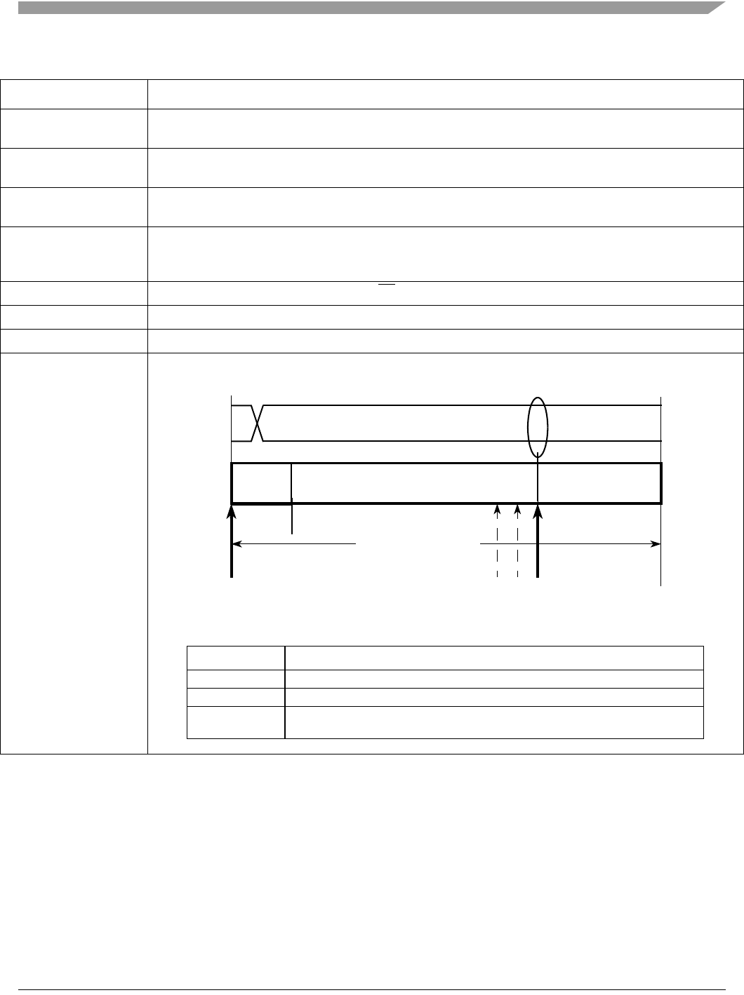
Terminology and Notational Conventions
MCF548x Reference Manual, Rev. 3
Freescale Semiconductor liii
Table 10-3/10-5 Bits BA, DT, and AT: The 0 and 1 are switched. Setting each bit enables operation, while clearing disables
operation. The 0 and 1 (or the corresponding descriptions) need to be swapped for all three bits.
11.4.2/11-8 Remove all text from bullet item #2 starting with “This scenario works for all pulses except....” This errata
does not apply to this processor.
13.1.1/13-1 Correct the cross-reference link at top of page that reads “Section 3.8.1, ‘Exception Stack Frame
Definition.’”
Table 15-27/15-24 In the bit 7-6, PAR1_E1MDC entry, change ‘11’ bit setting description from: “E1MDC pin configured for
FEC1 MDC function” to “E1MDC pin configured for FEC1 E1MDC function” to be consistent with rest of
section.
Table 15-34/15-30 Remove extraneous “/” from “DSPICS0//SS” in second sentence of the PAR_CS0 bit description.
Table 16-1/16-2 Extend SSCR entry to include bytes 2 & 3 as well as bytes 0 and 1, since it is a 32 bit register.
17.6.5.4.2/17-23 Change “transfer start” to “address latch enable” in second sentence.
21.4.9/21-28 Figure 21-14 and Table 21-18 are missing. Add them as shown below and correct the cross-references to
them.
Table iv. MCF548x Revision History (continued)
Section/Page Substantive Changes
Figure 21-14. Segments within the Bit Time
Table 21-18. Time Segment Syntax
Syntax Description
SYNC_SEG System expects transitions to occur on the bus during this period.
Transmit Point A node in transmit mode transfers a new value to the CAN bus at this point.
Sample Point A node samples the bus at this point. If the three samples per bit option is selected,
then this point marks the position of the third sample.
SYNC_SEG Time Segment 1 Time Segment 2
1 4 ... 16 2 ... 8
8 ... 25 Time Quanta
= 1 Bit Time
NRZ Signal
Sample Point
(single or triple sampling)
(PROP_SEG + PSEG1 + 2) (PSEG2 + 1)
Transmit Point

MCF548x Reference Manual, Rev. 3
liv Freescale Semiconductor
21.4.9/21-28 Add the following table below the note at the end of the section and correct the cross-reference pointing to
it:
Table 23-5/23-7 The JTAG IR codes are incorrect. Replace table with the following:
23.4.3/23-7 Remove the TEST_LEAKAGE section, as the instruction is not supported.
23.4.3/23-7 Remove the LOCKOUT_RECOVERY section, as the instruction is not supported.
Table 24-18/24-20 Correct Base Address Mask Register 1 mnemonic from EREQMASK0 to EREQMASK1.
24.3.4.2/24-20 Correct overbar in first sentence. From “After DREQ is asserted, this register contains...” to “After DREQ
is asserted, this register contains...”
Table iv. MCF548x Revision History (continued)
Section/Page Substantive Changes
Table 21-19. CAN Standard Compliant Bit Time Segment Settings
Time Segment 1 Time Segment 2 Re-synchronization
Jump Width
5 .. 10 2 1 .. 2
4 .. 11 3 1 .. 3
5 .. 12 4 1 .. 4
6 .. 13 5 1 .. 4
7 .. 14 6 1 .. 4
8 .. 15 7 1 .. 4
9 .. 16 8 1 .. 4
F
Instruction IR[5:0] Instruction Summary
EXTEST 000000 Selects boundary scan register while applying fixed values to output
pins and asserting functional reset
SAMPLE 000001 Selects boundary scan register for shifting, sampling, and preloading
without disturbing functional operation
IDCODE 011101 Selects IDCODE register for shift
CLAMP 011111 Selects bypass while applying fixed values to output pins and
asserting functional reset
HIGHZ 111101 Selects bypass register while tri-stating all output pins and asserting
functional reset
ENABLE 000010 Selects TEST_CTRL register
BYPASS 111111 Selects bypass register for data operations

Terminology and Notational Conventions
MCF548x Reference Manual, Rev. 3
Freescale Semiconductor lv
25.1.2/25-2 Add the following section after section 24.1.2:
24.1.3 Comm Timer External Clock[7:0]
The comm timer external clock is the alternate clock signal and is provided by the user. The user must write
a 1 to CTCR[S] in the variable channel and write a 1001 to CTCR[S] within the fixed channel to select this
signal. If this signal is selected, all timing will be with respect to this clock signal. This signal is restricted to
being half the frequency or less of the system bus clock.
Table 25-3/25-5 In the S bit description change the 1001 setting from “Reserved” to “External clock”
Table 25-4/25-6 The S bit field is incorrect. Bits 31-29 should be reserved, and only bit 28 should be the S bit. And the S bit
description should be:
Clock enable source select. Selects the clock rate for the fixed timer channels. The clock rate for the timer
is the internal system clock divided by an 8-bit prescaler.
1 External Clock
0 Sysclk
Note: The external bus clock cannot be an faster than half the frequency of the system clock.
26.1/26-1 Fix broken cross-reference to Figure 26-1.
Table 26-13/26-19 In description of TXRDY change PSCTFALARM to PSCTFAR
Table 26-30/26-29 In description of ALARM change instance of “less than alarm bytes” to “more than alarm bytes” and change
instance of “more than alarm bytes” to “less than alarm bytes”.
26.3.3.24/26-30 Change bit 30 to reserved, as the WFR field is only one-bit wide.
Figure 26-22/Page
26-32
Remove shading from W field as the PSCRFARn and PSCTFARn registers are R/W accessible.
26.4/26-35 Add section 15.3.7 “PSC FIFO System” from the MPC5200 User’s Manual to before section 26.4.9
“Looping Modes.” Change the following text to apply to the MCF548x:
MPC5200 → MCF5478x
BestComm → Multichannel DMA
MR1 → PSCMR1n
SR→ PSCSRn
ORERR → ERR
Figure 28-1/Page 28-1 Change IFDR to I2FDR and IADR to I2ADR in figure.
28.3.2.1/28-3 Change instances of I2AR to I2ADR.
28.3.2.3/28-5 Change I2ICR to I2CR throughout section.
Chapter 28, “I2C
Interface”
After section 27.3.2.4, change instances of R/W to R/W throughout chapter.
Table iv. MCF548x Revision History (continued)
Section/Page Substantive Changes
Table 0-4. Comm Timers External Clock
Timer Channel External Signal
0TIN0
1TIN1
2TIN2
3TIN3
4PSC3BCLK
5PSC2BCLK
6PSC1BCLK
7PSC0BCLK

MCF548x Reference Manual, Rev. 3
lvi Freescale Semiconductor
27.6.1/27-5 Remove instances of MDIS bit as it is not present on this version of the DSPI.
Table 29-3/29-11 USBCR[APPLOCK] bit description, the bit setting numbers are incorrrect. When cleared (0), APPLOCK is
deasserted. When set (1), APPLOCK is asserted.
Table 29-29/29-30 Endpoint status register’s PSTALL entry: the last sentence should be “Setting this bit also sets
USBAISR[EPSTALL].” instead of “Setting this bit also sets USBAISR[EPHALT].”
Table 29-37/29-36 EPnISR[EOT] bit description, add a note to the last sentence of the first paragraph stating “The EOT
interrupt will not assert for an isochronous OUT packet that experiences a PID sequencing error.”
29.4.3.1/29-51 Add a section below USB Packets entitled “Handshakes” with the following paragraphs:
“The USB device will return a NYET handshake packet to an OUT transaction if there is already data
present in the FIFO and there are less than 2*MAXPACKETSIZE bytes free in the FIFO.
In cases where the FIFO depth is larger than 2*MAXPACKETSIZE (i.e. 3x or 4x), the following behavior
will occur. If after a transfer that returned a NYET handshake there is at least 1*MAXPACKETSIZE of free
space in the FIFO, the device will ACK the first PING request from the host and accept another
MAXPACKETSIZE transfer from the host. The device will again send a NYET handshake.
The only time the device will NAK a PING is when there is less than 1*MAXPACKETSIZE of free space in
the FIFO.”
Table 30-41/30-42 Change bit description of the FECFRST[SW_RST] bit to “Software Reset - This bit controls the soft reset
of the FEC FIFOs. A soft reset will reset the FIFO pointers and byte counters but not the status and control
registers. To cause a soft reset this bit should be set and then cleared by application software.”
Change bit description of the FECFRST[RST_CTL] bit to “Reset control - Setting this bit allows the FEC
controller to perform a soft reset of the FIFOs when the FEC is disabled (ECR[ETHER_EN] cleared).”
Table 31-1/31-1 Add column to indicate whether the signal has a pull-up resistor.
These signals have a pull-up resistor at all times:
DSCLK/TRST, BKPT/TMS, DSI/TDI
These signals have a pull-up resistor whenever configured for general-purpose input (default state after
reset):
PCIBR[4:3], PCIGNT[4:3], E1MDIO, E1MDC, E1TXCLK, E1TXEN, E1TXD[3:0], E1COL, E1RXCLK,
E1RXDV, E1RXD[3:0], E1CRS, E1TXER, E1RXER
Table 31-1/31-1 Ball P3 should be SD_VDD instead of EVDD.
Table 31-1/31-1 The GPIO bit number for each of the UART control signals are incorrect for Table 31-1. However, they are
correct for Table 2-1:
•Y23/PSC1RTS
pin: Change GPIO entry from PPSCL7 to PPSC1PSC06.
•AB23/PSC3RTS
pin: Change GPIO entry from PPSCH7 to PPSC3PSC26.
•AB26/PSC0RTS pin: Change GPIO entry from PPSCL3 to PPSC1PSC02.
• AC19/PSC2CTS pin: Change GPIO entry from PPSCH2 to PPSC3PSC23.
• AD26/PSC2RTS pin: Change GPIO entry from PPSCH3 to PPSC3PSC22.
•AE23/PSC0CTS pin: Change GPIO entry from PPSCL2 to PPSC1PSC03.
• AF23/PSC3CTS pin: Change GPIO entry from PPSCH6 to PPSC3PSC27.
• AF25/PSC1CTS pin: Change GPIO entry from PPSCL6 to PPSC1PSC07.
Table 31-1/31-1 Remove overbar from ALE at location AD6.
Table 31-1/31-1 • Replace PPSCLn entries under the GPIO column with PPSC1PSC0n. There is no PPSCL port.
• Replace PPSCHn entries under the GPIO column with PPSC3PSC2n. There is no PPSCH port.
Table iv. MCF548x Revision History (continued)
Section/Page Substantive Changes

Terminology and Notational Conventions
MCF548x Reference Manual, Rev. 3
Freescale Semiconductor lvii
Figure 31-3/Page 31-10 Remove overbar from ALE at location AD6.
Figure 31-7/Page 31-14 Remove overbar from ALE at location AD6.
Figure 31-11/Page
31-18
Remove overbar from ALE at location AD6.
Table iv. MCF548x Revision History (continued)
Section/Page Substantive Changes

MCF548x Reference Manual, Rev. 3
lviii Freescale Semiconductor

MCF548x Reference Manual, Rev. 3
Freescale Semiconductor 1-1
Chapter 1
Overview
This chapter provides an overview of the MCF548x microprocessor features, including the major
functional components.
1.1 MCF548x Family Overview
The MCF548x family is based on the ColdFire V4e core, a complex which comprises the ColdFire V4
central processor unit (CPU), an enhanced multiply-accumulate unit (EMAC), a memory management unit
(MMU), a double-precision floating point unit (FPU) conforming to standard IEEE-754, and controllers
for caches and local data memories. The MCF548x family is capable of performing at an operating
frequency of up to 200 MHz or 308 MIPS (Dhrystone 2.1).
To maximize throughput, the MCF548x family incorporates three independent external bus interfaces:
1. The general-purpose local bus (FlexBus) is used for system boot memories and simple peripherals
and has up to six chip selects.
2. Program code and data can be stored in SDRAM connected to a dedicated 32-bit double data rate
(DDR) bus that can run at up to one-half of the CPU core frequency. The glueless DDR SDRAM
controller handles all address multiplexing, input and output strobe timing, and memory bus clock
generation.
3. A 32-bit PCI bus compliant with the version 2.2 specification and running at a typical frequency
of 33 MHz or 66 MHz supports peripherals that require high bandwidth, the ability to arbitrate for
bus mastership, and access to internal MCF548x memory resources.
The MCF548x family provides substantial communications functionality by integrating the following
connectivity peripherals:
• Up to two 10/100 Mbps fast Ethernet controllers (FECs)
• One optional USB 2.0 device (slave) module with seven endpoints and an integrated transceiver
• Up to four UART/USART/IRDA/modem programmable serial controllers (PSCs)
• One DMA serial peripheral interface (DSPI)
• One inter-integrated circuit (I2C™) bus controller
• Two controller area network 2.0B (FlexCAN) interfaces with 16 message buffers each
Additionally, the MCF548x provides hardware support for a range of Internet security standards with an
optional bus-mastering cryptography accelerator. This module incorporates units to speed DES/3DES and
AES block ciphers, the RC4 stream cipher, bulk data hashing (MD5/SHA-1/SHA-256/HMAC), and
random number generation. Hardware acceleration of these functions is critical to avoiding the throughput
bottlenecks associated with software-only implementations of SSH, SSL/TLS, IPsec, SRTP, WEP, and
other security standards. The incorporation of cryptography acceleration makes the MCF548x family a
compelling solution for a wide range of office automation, industrial control, and SOHO networking
devices that must have the ability to securely transmit critical equipment control information across
typically insecure Ethernet data networks.
Additional features of MCF548x products include a watchdog timer, two 32-bit slice timers for RTOS
scheduling and alarm functionality, up to four 32-bit general-purpose timers with capture, compare, and
pulse width modulation capability, a multisource vectored interrupt controller, a phase-locked loop (PLL)
to generate the system clock, 32 Kbytes of SRAM for high-speed local data storage, and multiple
general-purpose I/O ports.
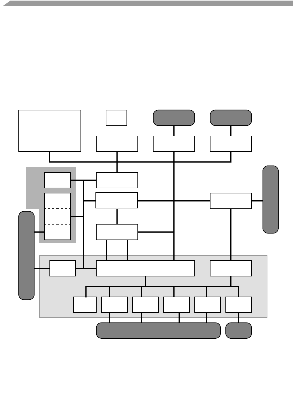
MCF548x Reference Manual, Rev. 3
1-2 Freescale Semiconductor
With on-chip support for multiple common communications interfaces, MCF548x products require only
the addition of memories and certain physical layer transceivers to be cost-effective system solutions for
many applications. Such applications include industrial routers, high-end POS terminals, building
automation systems, and process control equipment.
MCF548x products require four supply voltages: 1.5V for the high-performance, low power, internal core
logic, 2.5V for the DDR SDRAM bus interface, 1.25V for the DDR SDRAM VREF, and 3.3V for all other
I/O functionality, including the PCI and FlexBus interfaces.
1.2 MCF548x Block Diagram
Figure 1-1 shows a top-level block diagram of the MCF548x products.
1Available in MCF5485, MCF5484, MCF5483, and MCF5482 devices.
2Available in MCF5485, MCF5484, MCF5481, and MCF5480 devices.
3Available in MCF5485, MCF5483, and MCF5481 devices.
Figure 1-1. MCF548x Block Diagram
PLL DDR SDRAM
Memory
Controller
PCI I/O Interface and Ports
CommBus
USB 2.0
PHY1
Perpheral Communications I/O Interface & Ports
FEC22
PSC x 4I2CFEC1 USB 2.0
DEVICE1
Interface
FlexBus
Controller
FlexBus
Interface
PCI Interface
& FIFOs
Master/Slave
Interface
ColdFire V4e Core
FPU, MMU
EMAC
32K D-cache
32K I-cache
FlexCAN
x 2
Slave
Bus
DSPI
Perpheral I/O Interface & Ports
Communications
I/O Subsystem
Interrupt
Controller
XL Bus
Arbiter
System
Integration Unit
DMA
Read
DMA
Write
Multichannel DMA
Master Bus Interface and FIFOs
Slice
Timers x 2
GP
Timers x 4
Watchdog
Timer
PCI 2.2
Controller
Cryptography
32K System
SRAM
Crypto
R/W
XL Bus
Read/Write
XL Bus
Accelerator3

MCF548x Family Products
MCF548x Reference Manual, Rev. 3
Freescale Semiconductor 1-3
1.3 MCF548x Family Products
Table 1-1 summarizes the products available within the MCF548x product family. All products are
available in pin-compatible, 388-pin PBGA packaging allowing for ease of migration between products
within the family. A printed circuit board designed using the MCF5485/4 footprint is compatible with any
of the MCF548x family devices.
1.4 MCF548x Family Features
• ColdFire V4e core
— Limited superscalar V4 ColdFire processor core
— Up to 200 MHz peak internal core frequency (308 Dhrystone 2.1 MIPS)
— Harvard architecture
– 32-Kbyte instruction cache
– 32-Kbyte data cache
Table 1-1. MCF548x Family Products
Product Performance Features Temperature Range
MCF5485 308 MIPS
200 MHz
Two 10/100 Ethernet Controllers
Two CAN Controllers
USB 2.0 Device with Integrated PHY
v2.2 PCI Controller
DDR Memory Controller
Encryption Accelerator
-40 to 85 ° C
MCF5484 308 MIPS
200 MHz
Two 10/100 Ethernet Controllers
Two CAN Controllers
USB 2.0 Device with Integrated PHY
v2.2 PCI Controller
DDR Memory Controller
-40 to 85 ° C
MCF5483 255 MIPS
166 MHz
One 10/100 Ethernet Controller
Two CAN Controllers
USB 2.0 Device with Integrated PHY
v2.2 PCI Controller
DDR Memory Controller
Encryption Accelerator
-40 to 85 ° C
MCF5482 255 MIPS
166 MHz
One 10/100 Ethernet Controller
Two CAN Controllers
USB 2.0 Device with Integrated PHY
v2.2 PCI Controller
DDR Memory Controller
-40 to 85 ° C
MCF5481 255 MIPS
166 MHz
Two 10/100 Ethernet Controllers
Two CAN Controllers
v2.2 PCI Controller
DDR Memory Controller
Encryption Accelerator
-40 to 85 ° C
MCF5480 255 MIPS
166 MHz
Two 10/100 Ethernet Controllers
Two CAN Controllers
v2.2 PCI Controller
DDR Memory Controller
-40 to 85 ° C

MCF548x Reference Manual, Rev. 3
1-4 Freescale Semiconductor
— Memory management unit (MMU)
– Separate, 32-entry, fully-associative instruction and data translation lookahead buffers
— Floating point unit (FPU)
– Double-precision support that conforms to IEEE-754 standard
– Eight floating point registers
• Internal master bus (XLB) arbiter
— High performance split address and data transactions
— Support for various parking modes
• 32-bit double data rate (DDR) synchronous DRAM (SDRAM) controller
— 66–133 MHz operation
— Supports both DDR and SDR DRAM
— Built-in initialization and refresh
— Up to four chip selects enabling up to 1 GB of external memory
• Version 2.2 peripheral component interconnect (PCI) bus
— 32-bit target and initiator operation
— Support for up to five external PCI masters
— 33–66 MHz operation with PCI bus to XLB divider ratios of 1:1, 1:2, and 1:4
• Flexible multi-function external bus (FlexBus)
— Supports operation with the following:
– Non-multiplexed 32-bit address and 32-bit data (32-bit address muxed over
PCI bus–PCI not usable)
– Multiplexed 32-bit address and 32-bit data (PCI usable)
– Multiplexed 32-bit address and 16-bit data
– Multiplexed 32-bit address and 8-bit data
— Provides a glueless interface to boot Flash/ROM, SRAM, and peripheral devices
— Up to six chip selects
— 33–66 MHz operation
• Communications I/O subsystem
— Intelligent 16-channel DMA controller
— Dedicated DMA channels for receive and transmit on all subsystem peripheral interfaces
— Up to two 10/100 Mbps fast Ethernet controllers (FECs), each with separate 2-Kbyte receive
and transmit FIFOs
— Universal serial bus (USB) version 2.0 device controller
– Support for one control and six programmable endpoints — interrupt, bulk, or isochronous
– 4 Kbytes of shared endpoint FIFO RAM and 1 Kbyte of endpoint descriptor RAM
– Integrated physical layer interface
— Up to four programmable serial controllers (PSCs) each with separate 512-byte receive and
transmit FIFOs for UART, USART, modem, codec, and IrDA 1.1 interfaces
—I
2C peripheral interface
— Two FlexCAN controller area network 2.0B controllers each with 16 message buffers
— DMA serial peripheral interface (DSPI)
• Optional security encryption controller (SEC) module

MCF548x Family Features
MCF548x Reference Manual, Rev. 3
Freescale Semiconductor 1-5
— Execution units for the following:
– DES/3DES block cipher
– AES block cipher
– RC4 stream cipher
– MD5/SHA-1/SHA-256/HMAC hashing
– Random number generator compliant with FIPS 140-1 standards for randomness and
non-determinism
— Dual-channel architecture permits single-pass encryption and authentication
• 32-Kbyte system SRAM
— Arbitration mechanism shares bandwidth between internal bus masters (CPU, cryptography
accelerator, PCI, and DMA)
• System integration unit (SIU)
— Interrupt controller
— Watchdog timer
— Two 32-bit slice timers for periodic alarm and interrupt generation
— Up to four 32-bit general-purpose timers with capture, compare, and PWM capability
— General-purpose I/O ports multiplexed with peripheral pins
• Debug and test features
— Core debug support via ColdFire background debug mode (BDM) port
— Chip debug support via JTAG/ IEEE 1149.1 test access port
• PLL and clock generator
— 30–66.67 MHz input frequency range
• Operating Voltages
— 1.5V internal logic
— 2.5V DDR SDRAM bus I/O (1.25V VREF)
— 3.3V PCI, FlexBus, and all other I/O
• Estimated power consumption
— <1.5W
1.4.1 ColdFire V4e Core Overview
The ColdFire V4e core is a variable-length RISC, clock-multiplied core that includes a Harvard memory
architecture, branch cache acceleration logic, and limited superscalar dual-instruction issue capabilities.
The limited superscalar design approaches dual-issue performance with the cost of a scalar execution
pipeline.
The ColdFire V4e processor core is comprised of two separate pipelines that are decoupled by an
instruction buffer. The four-stage instruction fetch pipeline (IFP) prefetches the instruction stream,
examines it to predict changes of flow, partially decodes instructions, and packages fetched data into
instructions for the operand execution pipeline (OEP). The IFP can prefetch instructions before the OEP
needs them, minimizing the wait for instructions. The instruction buffer is a 10 instruction, first-in-first-out
(FIFO) buffer that decouples the IFP and OEP by holding prefetched instructions awaiting execution in
the OEP. The OEP includes five pipeline stages: the first stage decodes instructions and selects operands
(DS), and the second stage generates operand addresses (OAG). The third and fourth stages fetch operands
(OC1 and OC2), and the fifth stage executes instructions (EX).

MCF548x Reference Manual, Rev. 3
1-6 Freescale Semiconductor
The ColdFire V4e processor contains a double-precision floating point unit (FPU). The FPU conforms to
the American National Standards Institute (ANSI)/Institute of Electrical and Electronics Engineers (IEEE)
Standard for Binary Floating-Point Arithmetic (ANSI/IEEE Standard 754). The FPU operates on 64-bit,
double-precision floating point data and supports single-precision and signed integer input operands. The
FPU programming model is like that in the MC68060 microprocessor. The FPU is intended to accelerate
the performance of certain classes of embedded applications, especially those requiring high-speed
floating point arithmetic computations.
The ColdFire V4e processor also incorporates the ColdFire memory management unit (MMU), which
provides virtual-to-physical address translation and memory access control. The MMU consists of
memory-mapped control, status, and fault registers that provide access to translation lookaside buffers
(TLBs). Software can control address translation and access attributes of a virtual address by configuring
MMU control registers and loading TLBs. With software support, the MMU provides demand-paged,
virtual addressing.
The ColdFire V4e core implements the ColdFire instruction set architecture revision B with support for
floating Point instructions. Additionally, the ColdFire V4e core includes the enhanced
multiply-accumulate unit (EMAC) for improved signal processing capabilities. The EMAC implements a
4-stage execution pipeline, optimized for 32 x 32-bit operations, with support for four 48-bit accumulators.
Supported operands include 16- and 32-bit signed and unsigned integers, as well as signed fractional
operands and a complete set of instructions to process these data types. The EMAC provides superb
support for execution of DSP operations within the context of a single processor at a minimal hardware
cost.
Refer to Chapter 3, “ColdFire Core,” for detailed information on the ColdFire V4e core architecture.
1.4.2 Debug Module (BDM)
The ColdFire processor core debug interface is provided to support system debugging in conjunction with
low-cost debug and emulator development tools. Through a standard debug interface, users can access
real-time trace and debug information. This allows the processor and system to be debugged at full speed
without the need for costly in-circuit emulators.
The MCF548x debug module provides support in three different areas:
• Real-time trace support: The ability to determine the dynamic execution path through an
application is fundamental for debugging. The ColdFire solution implements an 8-bit parallel
output bus that reports processor execution status and data to an external BDM emulator system.
• Background debug mode (BDM): Provides low-level debugging in the ColdFire processor
complex. In BDM, the processor complex is halted and a variety of commands can be sent to the
processor to access memory and registers. The external BDM emulator uses a three-pin, serial,
full-duplex channel.
• Real-time debug support: BDM requires the processor to be halted, which many real-time
embedded applications cannot permit. Debug interrupts let real-time systems execute a unique
service routine that can quickly save key register and variable contents and return the system to
normal operation without halting. External development systems can access saved data, because
the hardware supports concurrent operation of the processor and BDM-initiated commands. In
addition, the option is provided to allow interrupts to occur.
1.4.3 JTAG
The MCF548x family supports circuit board test strategies based on the Test Technology Committee of
IEEE and the Joint Test Action Group (JTAG). The test logic includes a test access port (TAP) consisting
of a 16-state controller, an instruction register, and three test registers (a 1-bit bypass register, a 256-bit

MCF548x Family Features
MCF548x Reference Manual, Rev. 3
Freescale Semiconductor 1-7
boundary-scan register, and a 32-bit ID register). The boundary scan register links the device’s pins into
one shift register. Test logic, implemented using static logic design, is independent of the device system
logic. The MCF548x implementation can do the following:
• Perform boundary scan operations to test circuit board electrical continuity
• Sample MCF548x system pins during operation and transparently shift out the result in the
boundary scan register
• Bypass the MCF548x for a given circuit board test by effectively reducing the boundary-scan
register to a single bit
• Disable the output drive to pins during circuit-board testing
• Drive output pins to stable levels
1.4.4 On-Chip Memories
1.4.4.1 Caches
There are two independent caches associated with the ColdFire V4e core complex: a 32-Kbyte instruction
cache and a 32-Kbyte data cache. Caches improve system performance by providing single-cycle access
to the instruction and data pipelines. This decouples processor performance from system memory
performance, increasing bus availability for on-chip DMA or external devices.
1.4.4.2 System SRAM
The SRAM module provides a general-purpose 32-Kbyte memory block that the ColdFire core can access
in a single cycle. The location of the memory block can be set to any 32-Kbyte address boundary within
the 4-Gbyte address space. The memory is ideal for storing critical code or data structures, for use as the
system stack, or for storing FEC data buffers. Because the SRAM module is physically connected to the
processor's high-speed local bus, it can quickly service core-initiated accesses or memory-referencing
commands from the debug module.
The SRAM module is also accessible by multiple non-core bus masters, such as the DMA controller, the
encryption accelerator, and the PCI Controller.
1.4.5 PLL and Chip Clocking Options
MCF548x products contain an on-chip PLL capable of accepting input frequencies from 30–66.66 MHz.
Table 1-2 contains the frequencies of the system buses for the members of the MCF548x family under
various core/SDRAM/PCI/Flexbus clocking options.
Table 1-2. MCF548x Family Clocking Options
Core
(MHz)
Internal XLB, SDRAM
Bus, and PSTCLK
Frequency (MHz)
CLKIN—PCI and FlexBus
Frequency (MHz) Clock Ratio
120.0–200 60.0–100 30.0–50.0 1:2

MCF548x Reference Manual, Rev. 3
1-8 Freescale Semiconductor
1.4.6 Communications I/O Subsystem
1.4.6.1 DMA Controller
The communications subsystem contains an intelligent DMA unit that provides front line interrupt control
and data movement interface via a separate peripheral bus to the on-chip peripheral functions, leaving the
processor core free to handle higher level activities. This concurrent operation enables a significant boost
in overall system performance.
The communications subsystem can support up to 16 simultaneously enabled DMA tasks, with support for
up to two external DMA requests. It uses internal buffers to prefetch reads and post writes such that
bursting is used whenever possible. This optimizes both internal and external bus activity. The following
communications and computer control peripheral functions are integrated and controlled by the
communications subsystem:
• Up to two 10/100 Mbps fast Ethernet controllers (FECs)
• Optional universal serial bus (USB) version 2.0 device controller
• Up to four programmable serial controllers (PSCs)
•I
2C peripheral interface
• DMA serial peripheral interface (DSPI)
• Two FlexCAN controller area network 2.0B controllers
1.4.6.2 10/100 Fast Ethernet Controller (FEC)
The FEC supports two standard MAC/PHY interfaces: 10/100 Mbps IEEE 802.3 MII and 10Mbps 7-wire
interface. The controller is full duplex, supports a programmable maximum frame length and
retransmission from the transmit FIFO following a collision.
Support for different Ethernet physical interfaces:
— 100 Mbps IEEE 802.3 MII
— 10 Mbps IEEE 802.3 MII
— 10 Mbps 7-wire interface
• IEEE 802.3 full-duplex flow control.
• Support for full-duplex operation (200 Mbps throughput) with a minimum system clock frequency
of 50 MHz.
• Support for half duplex operation (100 Mbps throughput) with a minimum system clock frequency
of 25 MHz.
• Retransmit from transmit FIFO following collision.
• Internal loopback for diagnostic purposes.
1.4.6.3 USB 2.0 Device (Universal Serial Bus)
The USB module implementation on the MCF548x product family provides all the logic necessary to
process the USB protocol as defined by version 2.0 specification for peripheral devices. It features the
following:
• High-speed operation up to 480 Mbps, full-speed operation at 12 Mbps, and low-speed operation
at 1.5 Mbps
• Physical interface on chip
• Bulk, interrupt, and isochronous transport modes.
• Six programmable in/out endpoints and one control endpoint

MCF548x Family Features
MCF548x Reference Manual, Rev. 3
Freescale Semiconductor 1-9
• 4 Kbytes of shared endpoint FIFO RAM and 1 Kbyte of endpoint descriptor RAM
1.4.6.4 Programmable Serial Controllers (PSCs)
The MCF548x product family supports four PSCs that can be independently configured to operate in the
following modes:
• Universal asynchronous receiver transmitter (UART) mode
— 5,6,7,8 bits of data plus parity
— Odd, even, none, or force parity
— Stop bit width programmable in 1/16 bit increments
— Parity, framing, and overrun error detection
— Automatic PSCCTS and PSCRTS modem control signals
• IrDA 1.0 SIR mode (SIR)
— Baud rate range of 2400–115200 bps
— Selectable pulse width: either 3/16 of the bit duration or 1.6 µs
• IrDA 1.1 MIR mode (MIR)
— Baud rate of 0.576 or 1.152 Mbps
• IrDA 1.1 FIR mode (FIR)
— Baud rate of 4.0 Mbps
• 8-bit soft modem mode (modem8)
• 16-bit soft modem mode (modem16)
• AC97 soft modem mode (AC97)
Each PSC supports synchronous (USART) and asynchronous (UART) protocols. The PSCs can be used to
interface to external full-function modems or external codecs for soft modem support, as well as IrDA 1.1
or 1.0 interfaces. Both 8- and 16-bit data widths are supported. PSCs can be configured to support a
1200-baud plain old telephone system (POTS) modem, V.34 or V.90 protocols. The standard UART
interface supports connection to an external terminal/computer for debug support.
1.4.6.5 I2C (Inter-Integrated Circuit)
The MCF548x product family provides an I2C two-wire, bidirectional serial bus for on-board
communication. It features the following:
• Multimaster operation with arbitration and collision detection
• Calling address recognition and interrupt generation
• Automatic switching from master to slave on arbitration loss
• Software-selectable acknowledge bit
• Start and stop signal generation and detection
• Bus busy status detection
1.4.6.6 DMA Serial Peripheral Interface (DSPI)
The DSPI block operates as a basic SPI block with FIFOs providing support for external queue operation.
Data to be transmitted and data received reside in separate FIFOs. The FIFOs can be popped and pushed
by host software or by the system DMA controller. The DSPI supports these SPI features:
• Full-duplex, three-wire synchronous transfers
• Master and slave mode—two peripheral chip selects in master mode

MCF548x Reference Manual, Rev. 3
1-10 Freescale Semiconductor
• DMA support
1.4.6.7 Controller Area Network (CAN)
The FlexCAN modules are communication controllers implementing the CAN protocol. The CAN
protocol can be used as an industrial control serial data bus, meeting the specific requirements of real-time
processing and reliable operation in a harsh EMI environment, while maintaining cost-effectiveness. Each
of the two CAN controllers on the MCF548x family products contains sixteen message buffers. The CAN
controllers can be configured to either function as an interface with two separate CAN networks, or as a
single 32 message buffer CAN network.
1.4.7 DDR SDRAM Memory Controller
The DDR SDRAM memory controller is a glueless interface to DDR memories. The module uses a 32-bit
memory port and can address a maximum of 1 Gbyte of data with 16 64M x 8 (512-Mbit) devices, four
per chip select. The controller supplies two clock lines and respective inverted clock lines to help minimize
system complexity when using DDR. The module supports either DDR or SDR, but not both. This is due
to voltage differences between the memory technologies.
The supported memory clock rate is up to 133 MHz. At this memory clock rate, DDR memory can receive
data at an effective rate of up to 266 MHz.
• Support for up to 13 lines of row address, 11 lines of column address, two lines of bank address,
and up to four chip selects
• Memory bus width fixed at 32 bits
• Four chip selects support up to 1 GByte of SDRAM memory
• Support for page mode to maximize the data rate. Page mode remembers active pages for all four
chip selects
• Support for sleep mode and self refresh
• Cache line reads that can use critical word first. These reads can start in the center of a burst and
will wrap to the beginning. This allows the processor quicker access to a needed instruction.
All on-chip bus masters have access to DRAM. This includes PCI, the ColdFire V4e core, the
cryptography accelerator, and the DMA controller.
1.4.8 Peripheral Component Interconnect (PCI)
The PCI controller is a PCI V2.2-compliant bus controller and arbiter. The PCI bus is capable of 66-MHz
operation with a 32-bit address/data bus and support for five external masters.
The PCI module includes an inbound FIFO to increase performance when using an external bus master.
The bus can address all 4 Gbytes of PCI-addressable space.
The PCI bus is also multiplexed with the flexible local bus (FlexBus) address lines. If 32-bit non-muxed
local address and data is required, it can be obtained at the expense of utilizing the PCI bus.
When implemented, the PCI controller acts as the central resource, bus arbiter, and configuring master on
the PCI bus.
1.4.9 Flexible Local Bus (FlexBus)
The FlexBus module is intended to provide the user with basic functionality required to interface to
peripheral devices. The FlexBus interface is a multiplexed or non-multiplexed bus, with an operating

MCF548x Family Features
MCF548x Reference Manual, Rev. 3
Freescale Semiconductor 1-11
frequency from 33–66 MHz. The Flexbus is targeted to support external Flash memories, boot ROMs,
gate-array logic, or other simple target interfaces. Up to six chip selects are supported by the FlexBus.
Possible combinations of address and data bits are the following:
• Non-multiplexed 32-bit address and 32-bit data (32-bit address muxed over
PCI bus–PCI not usable)
• Multiplexed 32-bit address and 32-bit data (PCI usable)
• Multiplexed 32-bit address and 16-bit data
• Multiplexed 32-bit address and 8-bit data
The non-multiplexed 32-bit address and 32-bit data mode is determined at chip reset. For all other modes,
the full 32-bit address is driven during the address phase. The number of bytes used for data are determined
on a chip select by chip select basis.
1.4.10 Security Encryption Controller (SEC)
As consumers and businesses continue to embrace the Internet, the need for secure point-to-point
communications across what is an entirely insecure network has been met by the development of a range
of standard protocols. Computer cryptography fundamentally involves calculations with very large
numbers. Personal computers have sufficient processing power to implement these algorithms entirely in
software. When placed upon the embedded devices typically used for routing and remote access functions,
this same computational burden can potentially decrease the throughput of a 100 Mbps Ethernet interface
down to 10 Mbps.
Hardware acceleration of common cryptography algorithms is the solution to the computational bandwidth
requirements of Internet security standards. Discrete solutions currently address this problem, but the next
logical step is to integrate a cryptography accelerator on an embedded processor, such as the MCF548x
family.
Freescale has developed the SEC on the MCF548x family for this purpose. This block accelerates the core
cryptography algorithms that underlie standard Internet security protocols like SSL/TLS, IPSec, IKE, and
WTLS/WAP.
• The SEC includes execution units for the following:
— DES/3DES block cipher
— AES block cipher
— RC4 stream cipher
— MD5/SHA-1/SHA-256/HMAC hashing
— Random number generator compliant with FIPS 140-1 standards for randomness and
non-determinism
• Dual-channel architecture permits single-pass encryption and authentication
1.4.11 System Integration Unit (SIU)
1.4.11.1 Timers
The MCF548x family integrates several timer functions required by most embedded systems. Two internal
32-bit slice timers create short cycle periodic interrupts, typically utilized for RTOS scheduling and alarm
functionality. A watchdog timer resets the processor if not regularly serviced, catching software hang-ups.
Four 32-bit general purpose timers can perform input capture, output compare, and PWM functionality.

MCF548x Reference Manual, Rev. 3
1-12 Freescale Semiconductor
1.4.11.2 Interrupt Controller
The interrupt controller on the MCF548x family can support up to 63 interrupt sources. The interrupt
controller is organized as seven levels with nine interrupt sources per level. Each interrupt source has a
unique interrupt vector, and 56 of the 63 sources of a given controller provide a programmable level [1-7]
and priority within the level.
• Support for up to 63 interrupt sources organized as follows:
— 56 fully-programmable interrupt sources
— 7 fixed-level interrupt sources
• Seven external interrupt signals
• Unique vector number for each interrupt source
• Ability to mask any individual interrupt source or all interrupt sources (global mask-all)
• Support for hardware and software interrupt acknowledge (IACK) cycles
• Combinatorial path to provide wake-up from stop mode
1.4.11.3 General Purpose I/O
All peripheral I/O pins on the MCF548x family are multiplexed with GPIO, adding flexibility and usability
to all signals on the chip.

MCF548x Reference Manual, Rev. 3
Freescale Semiconductor 2-1
Chapter 2
Signal Descriptions
2.1 Introduction
This chapter describes the MCF548x signals.
NOTE
The terms ‘assertion’ and ‘negation’ are used to avoid confusion when
dealing with a mixture of active-low and active-high signals. The term
‘asserted’ indicates that a signal is active, independent of the voltage level.
The term ‘negated’ indicates that a signal is inactive.
Active-low signals, such as RAS and TA, are indicated with an overbar.
2.1.1 Block Diagram
Figure 2-1 displays the signals of the MCF548x.
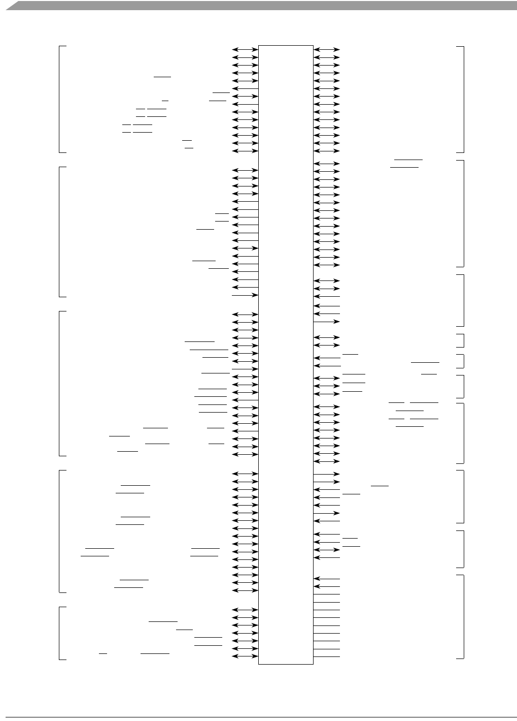
MCF548x Reference Manual, Rev. 3
2-2 Freescale Semiconductor
Figure 2-1. MCF548x Signals
MCF548x
E0MDIO / PFECI2C3
E0CRS / PFEC0H0
E0TXD[3:1] / PFEC0L[7:5]
E0TXER / PFEC0L4
E0RXD[3:1] / PFEC0L[3:1]
E0RXER / PFEC0L0
E1MDIO / SDA / CANRX0
E1MDC / SCL / CANTX0
E1TXCLK / PFEC1H7
E1TXEN / PFEC1H6
E1TXD0 / PFEC1H5
E1COL / PFEC1H4
E1RXCLK / PFEC1H3
E1RXDV / PFEC1H2
E1RXD0 / PFEC1H1
E1CRS / PFEC1H0
E1TXD[3:1] / PFEC1L[7:5]
E1TXER / PFEC1L4
E1RXD[3:1] / PFEC1L[3:1]
E1RXER / PFEC1L0
USBD+
USBD–
USBVBUS
USBRBIAS
SDA / PFECI2C1
SCL / PFECI2C0
AD[31:24]
SDDATA[31:24]
SDDATA[23:16]
SDDATA[15:8]
SDDATA[7:0]
SDADDR[12:0]
SDBA[1:0]
RAS
CAS
SDCS[3:0]
SDDM[3:0]
SDDQS[3:0]
SDCLK[1:0]
SDCLK[1:0]
SDWE
PCIAD[31:24] / FBADDR[31:24]
PCIAD[23:16] / FBADDR[23:16]
PCIAD[15:8] / FBADDR[15:8]
PCIAD[7:0] / FBADDR[7:0]
PCICXBE[3:0]
PCIDEVSEL
PCIFRM
PCIIDSEL
PCIIRDY
PCIPAR
PCIPERR
PCIRESET
PCISERR
PCISTOP
PCITRDY
PCIBG4 / PPCIBG4 / TBST
PCIBG[3:0] / PPCIBG[3:0] / TOUT[3:0]
PCIBR4 / PPCIBR4 / IRQ4
AD[23:16]
AD15:8]
AD[7:0]
FBCS[5:1] / PFBCS[5:1]
FBCS0
ALE / PFBCTL0 / TBST
R/W / PFBCTL2 / TBST
BE/BWE3 / PFBCTL7 / TSIZ1
BE/BWE2 / PFBCTL6 / TSIZ0
BE/BWE1 / PFBCTL5 / FBADDR1
BE/BWE0 / PFBCTL4 / FBADDR0
OE / PFBCTL3
TA / PFBCTL1
E0MDC / PFECI2C2
E0TXCLK / PFEC0H7
E0TXD0 / PFEC0H5
E0COL / PFEC0H4
E0RXCLK / PFEC0H3
E0RXDV / PFEC0H2
E0RXD0 / PFEC0H1
E0TXEN / PFEC0H6
SDCKE
SDRDQS
VREF
PCIBR[3:0] / PPCIBR[3:0] / TIN[3:0]
USBCLKIN
USBCLKOUT
PCS0TXD / PPSCL0
PSC0RXD / PPSCL1
PSC0CTS / PPSCL2 / PSC0BCLK
PSC0RTS / PPSCL3 / PSC0FSYNC
PSC1TXD / PPSCL4
PSC1RXD / PPSCL5
PSC1CTS / PPSCL6 / PSC1BCLK
PSC1RTS / PPSCL7 / PSC1FSYNC
PSC2TXD / PPSCH0
PSC2RXD / PPSCH1
PSC2CTS / PPSCH2 / PSC2BCLK / CANRX0
PSC2RTS / PPSCH3 / PSC2FSYNC / CANTX0
PSC3TXD / PPSCH4
PSC3RXD / PPSCH5
PSC3CTS / PPSCH6 / PSC3BCLK
PSC3RTS / PPSCH7 / PSC3FSYNC
IRQ7 / PIRQ7
IRQ[6:5] / PIRQ[6:5] / CANRX1
DREQ1 / PDMA1 / TIN1 / IRQ1
DREQ0 / PDMA0 / TIN0
DACK[1:0] / PDMA[3:2] / TOUT[1:0]
TIN3 / PTIM7 / IRQ3 / CANRX1
TOUT3 / PTIM6 / CANTX1
TIN2 / PTIM5 / IRQ2 / CANRX1
TOUT2 / PTIM4 / CANTX1
TIN1
TOUT1
TIN0
TOUT0
PSTCLK
PSTDDATA[7:0]
DSCLK / TRST
BKPT / TMS
DSI / TDI
DSO / TDO
TCK
DSPISOUT / PDSPI0 / PSC3TXD
DSPISIN / PDSPI1 / PSC3RXD
DSPISCK / PDSPI2 / PSC3CTS / PSC3BCLK
DSPICS5/PCSS / PDSPI6
DSPICS3 / PDSPI5 / TOUT3 / CANTX1
DSPICS2 / PDSPI4 / TOUT2 / CANTX1
EVDD
IVDD
VSS
SDVDD
PLLVDD
PLLVSS
USB_OSCVDD
USB_PHYVDD
USB_OSCAVDD
USB_PLLVDD
USBVDD
DSPICS0/SS / PDSPI3 / PSC3RTS / PSC3FSYNC
MTMOD[3:0]
RSTI
RSTO
CLKIN
FlexBus
SDRAM
Controller
PCI
Controller
Ethernet
MAC 0
Ethernet
MAC 1
USB
External
Interrupts
Port
I2C
DMA
Controller
Timer
Module
Debug &
JTAG
Test Port
Control
Test /
Reset &
Clock
Power
Supplies
PSCs
DSPI

Introduction
MCF548x Reference Manual, Rev. 3
Freescale Semiconductor 2-3
Table 2-1 lists the signals for the MCF548x in functional group order.
Table 2-1. MCF548x Signal Description
PBGA Pin
Pin Functions
Description I/O
Pull-up
Drive
Reset
State
Primary GPIO Secondary Tertiary
FlexBus
AE2, AF3, AF1,
AE3, AE4, AD5,
AF2, AD4
AD[31:24] — — — Multiplexed
address/data bus
I/O 16 Hi-Z
AD3, AC3, AD2,
AC2, AA4, AE1,
AC1, AD1
AD[23:16] — — — Multiplexed
address/data bus
I/O 16 Hi-Z
AB2, AA3, W4,
AB1, AA2, AA1,
Y1, Y2
AD[15:8] — — — Multiplexed
address/data bus
I/O 16 Hi-Z
W3, W1, W2, V3,
V1, V2, T4, U3
AD[7:0] — — — Multiplexed
address/data bus
I/O 16 Hi-Z
R1, T2, T3, T1, U2 FBCS[5:1] PFBCS[5:1] — — Chip selects 5–1 O:I/O 24 High
U1 FBCS0 — — — Chip select 0 O 24 High
AD6 ALE PFBCTL0 TBST — Address Latch Enable O:I/O 16 High
AE5 R/W PFBCTL2 TBST — Read/write O:I/O 16 Hi-Z
AF4 BE/BWE3 PFBCTL7 TSIZ1 — Byte enables O:I/O 16 High
AF5 BE/BWE2 PFBCTL6 TSIZ0 — Byte enables O:I/O 16 High
AC4 BE/BWE1 PFBCTL5 FBADDR1 — Byte enables O:I/O 16 High
AE7 BE/BWE0 PFBCTL4 FBADDR0 — Byte enables O:I/O 16 High
AE6 OE PFBCTL3 — — Output enable O:I/O 16 High
AF6 TA PFBCTL1 — — Transfer acknowledge I:I/O 16 —
SDRAM Controller
C10, B9, A8, D5,
A6, C8, B7, A5
SDDATA[31:24] — — — SDRAM data bus I/O 24 Hi-Z
A4, C7, B6, B4,
C5, B3, C4, D4
SDDATA[23:16] — — — SDRAM data bus I/O 24 Hi-Z
E2, D1, G4, E1,
K4, F1, G2, H3
SDDATA[15:8] — — — SDRAM data bus I/O 24 Hi-Z
N4, G1, H2, J3,
J1, M4, K3, K2
SDDATA[7:0] — — — SDRAM data bus I/O 24 Hi-Z
A13, A12, D10,
B12, C12, A11,
D8, B11, C11,
A10, D7, B10, A9
SDADDR[12:0] — — — SDRAM address bus O 24 Low

MCF548x Reference Manual, Rev. 3
2-4 Freescale Semiconductor
M2, M3 SDBA[1:0] — — — SDRAM bank
addresses
O24Low
E3 RAS — — — SDRAM row address
strobe
O24High
C2 CAS — — — SDRAM column
address strobe
O24High
R2, P2, P1, N3 SDCS[3:0] — — — SDRAM chip selects O 24 High
B8, A3, G3, J2 SDDM[3:0] — — — SDRAM write data
byte mask
O24High
A7, B5, F2, H1 SDDQS[3:0] — — — SDRAM data strobe I/O 24 High
L1, N1 SDCLK[1:0] — — — SDRAM clock O 24 Low
M1, N2 SDCLK[1:0] — — — Inverted SDRAM
clock
O24Low
K1 SDWE — — — SDRAM write enable O 24 Low
E4 SDCKE — — — SDRAM clock enable O 24 Low
L2 SDRDQS — — — SDR SDRAM data
strobe
O24Low
D2 VREF — — — SDRAM reference
voltage
I——
PCI Controller
V25, V26, U25,
U26, T24, T25,
T26, R24
PCIAD[31:24] — FBADDR[31:24] — PCI address/data bus I/O 16 Hi-Z
R25, R26, P26,
P24, P23, P25,
N25, N23
PCIAD[23:16] — FBADDR[23:16] — PCI address/data bus I/O 16 Hi-Z
N26, N24, M26,
M25, L26, L25,
K26, K25
PCIAD[15:8] — FBADDR[15:8] — PCI address/data bus I/O 16 Hi-Z
J26, K24, J25,
H26, J24, G26,
H25, K23
PCIAD[7:0] — FBADDR[7:0] — PCI address/data bus I/O 16 Hi-Z
F26, G25, E26,
G24
PCICXBE[3:0] — — — PCI command/byte
enables
I/O 16 Hi-Z
J23 PCIDEVSEL ———PCI device select I/O 16 Hi-Z
F25 PCIFRM ———PCI frame I/O 16 Hi-Z
C23 PCIIDSEL — — — PCI initialization
device select
I — —
Table 2-1. MCF548x Signal Description (Continued)
PBGA Pin
Pin Functions
Description I/O
Pull-up
Drive
Reset
State
Primary GPIO Secondary Tertiary

Introduction
MCF548x Reference Manual, Rev. 3
Freescale Semiconductor 2-5
D24 PCIIRDY ———PCI initiator ready I/O 16 Hi-Z
F23 PCIPAR — — — PCI parity I/O 16 Hi-Z
D26 PCIPERR ———PCI parity error I/O 16 Hi-Z
G23 PCIRESET ———PCI reset O16 Low
F24 PCISERR ———PCI system error I/O 16 Hi-Z
E25 PCISTOP ———PCI stop I/O 16 Hi-Z
C26 PCITRDY — — — PCI target ready I/O 16 Hi-Z
W24 PCIBG4 PPCIBG4 TBST —PCI external grant 4 O:I/O 16 GPI
Y26, W25, V24,
W26
PCIBG[3:0] PPCIBG[3:0] TOUT[3:0] — PCI external grant 3–0 O:I/O 16 GPI
D21 PCIBR4 PPCIBR4 IRQ4 —PCI external
request 4
I:I/O Y18GPI
B24 PCIBR3 PPCIBR3 TIN3 — PCI external
request 3
I:I/O Y18GPI
A25, B23, A24 PCIBR[2:0] PPCIBR[2:0] TIN[2:0] — PCI external
request 2–0
I:I/O 8GPI
External Interrupts Port
D14 IRQ7 PIRQ7 — — External interrupt
request 7
I:I/O — —
B14, A14 IRQ[6:5] PIRQ[6:5] CANRX1 —External interrupt
request 6–5
I:I/O — —
Ethernet MAC 0
AF10 E0MDIO PFECI2C3 — — Management channel
serial data
I/O 8GPI
AD11 E0MDC PFECI2C2 — — Management channel
clock
O:I/O 8GPI
AF9 E0TXCLK PFEC0H7 — — MAC transmit clock I:I/O 8GPI
AE10 E0TXEN PFEC0H6 — — MAC transmit enable O:I/O 8GPI
AD9 E0TXD0 PFEC0H5 — — MAC transmit data O:I/O 8GPI
AC9 E0COL PFEC0H4 — — MAC collision I:I/O 8GPI
AD14 E0RXCLK PFEC0H3 — — MAC receive clock I:I/O 8GPI
AE14 E0RXDV PFEC0H2 — — MAC receive enable I:I/O 8GPI
AD13 E0RXD0 PFEC0H1 — — MAC receive data I:I/O 8GPI
AE19 E0CRS PFEC0H0 — — MAC carrier sense I:I/O 8GPI
Table 2-1. MCF548x Signal Description (Continued)
PBGA Pin
Pin Functions
Description I/O
Pull-up
Drive
Reset
State
Primary GPIO Secondary Tertiary

MCF548x Reference Manual, Rev. 3
2-6 Freescale Semiconductor
AD8, AC6, AF7 E0TXD[3:1] PFEC0L[7:5] — — MAC transmit data O:I/O 8GPI
AE9 E0TXER PFEC0L4 — — MAC transmit error O:I/O 8GPI
AF11, AF12,
AF13
E0RXD[3:1] PFEC0L[3:1] — — MAC receive data I:I/O 8GPI
AC14 E0RXER PFEC0L0 — — MAC receive error I:I/O 8GPI
Ethernet MAC 1
AE252E1MDIO —SDA CANRX0 Management channel
serial data
I/O Y18 —
AD242E1MDC —SCL CANTX0 Management channel
clock
O:I/O Y18 —
AE132E1TXCLK PFEC1H7 — — MAC Transmit clock I:I/O Y18GPI
AD252E1TXEN PFEC1H6 — — MAC Transmit enable O:I/O Y18GPI
AE122E1TXD0 PFEC1H5 — — MAC Transmit data O:I/O Y18GPI
AF82E1COL PFEC1H4 — — MAC Collision I:I/O Y18GPI
B222E1RXCLK PFEC1H3 — — MAC Receive clock I:I/O Y18GPI
B252E1RXDV PFEC1H2 — — MAC Receive enable I:I/O Y18GPI
AF242E1RXD0 PFEC1H1 — — MAC Receive data I:I/O Y18GPI
AC52E1CRS PFEC1H0 — — MAC Carrier sense I:I/O Y18GPI
AC82, AC112,
AE112E1TXD[3:1] PFEC1L[7:5] — — MAC Transmit data O:I/O Y18GPI
AE242E1TXER PFEC1L4 — — MAC Transmit error O:I/O Y18GPI
D252, B262, A262E1RXD[3:1] PFEC1L[3:1] — — MAC Receive data I:I/O Y18GPI
AE82E1RXER PFEC1L0 — — MAC Receive error I:I/O Y18GPI
USB
AF163USBD+ — — — USB differential data I/O 24 —
AF173USBD- — — — USB differential data I/O 24 —
AC173USBVBUS — — — USB Vbus monitor
input
I — —
AF18 USBRBIAS — — — USB bias resistor I — —
AF153USBCLKIN — — — USB crystal input I — —
AF143USBCLKOUT — — — USB crystal output O24 —
DSPI
Y24 DSPISOUT PDSPI0 PSC3TXD —QSPI data out O:I/O 24 GPI
Table 2-1. MCF548x Signal Description (Continued)
PBGA Pin
Pin Functions
Description I/O
Pull-up
Drive
Reset
State
Primary GPIO Secondary Tertiary

Introduction
MCF548x Reference Manual, Rev. 3
Freescale Semiconductor 2-7
AC24 DSPISIN PDSPI1 PSC3RXD —QSPI data in I:I/O 24 GPI
AD22 DSPISCK PDSPI2 PSC3CTS PSC3BCLK QSPI clock I/O 24 GPI
W23 DSPICS5/PCSS PDSPI6 — — QSPI chip select O:I/O 24 GPI
V23 DSPICS3 PDSPI5 TOUT3 CANTX1 QSPI chip select O:I/O 24 GPI
AA26 DSPICS2 PDSPI4 TOUT2 CANTX1 QSPI chip select O:I/O 24 GPI
Y25 DSPICS0/SS PDSPI3 PSC3RTS PSC3FSYNC QSPI chip select O:I/O 24 GPI
I2C
C24 SDA PFECI2C1 — — I2C Serial data I/O 8GPI
C25 SCL PFECI2C0 — — I2C Serial clock I/O 8GPI
PSCs
AA25 PSC0TXD PPSC1PSC00 — — PSC0 transmit data O:I/O 8GPI
AC21 PSC0RXD PPSC1PSC01 — — PSC0 receive data I:I/O 8GPI
AE23 PSC0CTS PPSC1PSC03 PSC0BCLK —PSC0 clear to send I:I/O 8GPI
AB26 PSC0RTS PPSC1PSC02 PSC0FSYNC —PSC0 request to send I/O 8GPI
AB25 PSC1TXD PPSC1PSC04 — — PSC1 transmit data O:I/O 8GPI
AE22 PSC1RXD PPSC1PSC05 — — PSC1 receive data I:I/O 8GPI
AF25 PSC1CTS PPSC1PSC07 PSC1BCLK —PSC1 clear to send I:I/O 8GPI
Y23 PSC1RTS PPSC1PSC06 PSC1FSYNC —PSC1 request to send I/O 8GPI
AC26 PSC2TXD PPSC3PSC20 — — PSC2 transmit data O:I/O 8GPI
AD21 PSC2RXD PPSC3PSC21 — — PSC2 receive data I:I/O 8GPI
AC19 PSC2CTS PPSC3PSC23 PSC2BCLK CANRX0 PSC2 clear to send I:I/O 8GPI
AD26 PSC2RTS PPSC3PSC22 PSC2FSYNC CANTX0 PSC2 request to send I/O 8GPI
AE26 PSC3TXD PPSC3PSC24 — — PSC3 transmit data O:I/O 8GPI
AE21 PSC3RXD PPSC3PSC25 — — PSC3 receive data I:I/O 8GPI
AF23 PSC3CTS PPSC3PSC27 PSC3BCLK —PSC3 clear to send I:I/O 8GPI
AB23 PSC3RTS PPSC3PSC26 PSC3FSYNC —PSC3 request to send I/O 8GPI
DMA Controller
AF19 DREQ1 PDMA1 TIN1 IRQ1 DMA request I:I/O 8GPI
AF20 DREQ0 PDMA0 TIN0 —DMA request I:I/O 8GPI
AC25, AB24 DACK[1:0] PDMA[3:2] TOUT[1:0] —DMA acknowledge O:I/O 8GPI
Table 2-1. MCF548x Signal Description (Continued)
PBGA Pin
Pin Functions
Description I/O
Pull-up
Drive
Reset
State
Primary GPIO Secondary Tertiary

MCF548x Reference Manual, Rev. 3
2-8 Freescale Semiconductor
Timer Module
AD19 TIN3 PTIM7 IRQ3 CANRX1 Timer input I:I/O 8GPI
AD23 TOUT3 PTIM6 CANTX1 —Timer output O:I/O 8GPI
AF21 TIN2 PTIM5 IRQ2 CANRX1 Timer input I:I/O 8GPI
AC22 TOUT2 PTIM4 CANTX1 —Timer output O:I/O 8GPI
AE20 TIN1 — — — Timer input I 8 GPI
AC23 TOUT1 — — — Timer output O 8 GPI
AF22 TIN0 — — — Timer input I 8 GPI
AF26 TOUT0 — — — Timer output O 8 GPI
Debug and JTAG Test Port Control
D20 PSTCLK — — — Processor clock
output
O 8 High
A23, B21, D18,
C20, A22, B20,
A21, B19
PSTDDATA[7:0] — — — Processor status
debug data
O 8 High
C15 DSCLK —TRST —Debug clock / TAP
reset
I Y — —
B15 BKPT —TMS —Breakpoint/TAP test
mode select
I Y — —
A15 DSI —TDI —Debug data in / TAP
data in
I Y — —
D17 DSO —TDO —Debug data out / TAP
data out
O 8 High
A16 TCK — — — TAP clock I — —
Test, Reset, and Clock
B17, C14, A18,
B16
MTMOD[3:0] — — — Test mode pins I — —
B13 RSTI — — — Reset input I — —
A20 RSTO — — — Reset output O 8 Low
A17 CLKIN — — — Clock input I — —
D15 NC — — — No Connect I — —
AC15 NC — — — No Connect I — —
Table 2-1. MCF548x Signal Description (Continued)
PBGA Pin
Pin Functions
Description I/O
Pull-up
Drive
Reset
State
Primary GPIO Secondary Tertiary

Introduction
MCF548x Reference Manual, Rev. 3
Freescale Semiconductor 2-9
Power Supplies
C16, C22, E24,
H24, M24, R3,
U24, Y3, AA24,
AB3, AD7, AD10,
AD18
EVDD — — — Positive I/O supply I — —
C18, D11, D12,
D19, D22, H4,
H23, L23, P4,
R23, V4, AA23,
AC12, AC20
IVDD — — — Positive core supply I — —
A2, B2, C3, C17,
C19, C21, D6, D9,
D13, D16, D23,
E23, F4, J4, L4,
L11, L12, L13,
L14, L15, L16,
L24, M11, M12,
M13, M14, M15,
M16, M23, N11,
N12, N13, N14,
N15, N16, P11,
P12, P13, P14,
P15, P16, R4,
R11, R12, R13,
R14, R15, R16,
T11, T12, T13,
T14, T15, T16,
T23, U4, U23, Y4,
AB4, AC7, AC10,
AC18, AD12,
AD17, AD20,
AE15, AE16,
AE17
VSS — — Ground
A1, B1, C1, C6,
C9, C13, D3, F3,
L3, P3
SDVDD — — — Positive SDRAM
supply
A19 PLLVDD — — — Positive PLL analog
supply
B18 PLLVSS — — — PLL ground
AC134USB_OSCVDD — — — USB oscillator supply
AC164USB_PHYVDD — — — USB PHY supply
AD154USB_OSCAVDD — — — USB oscillator analog
supply
Table 2-1. MCF548x Signal Description (Continued)
PBGA Pin
Pin Functions
Description I/O
Pull-up
Drive
Reset
State
Primary GPIO Secondary Tertiary

MCF548x Reference Manual, Rev. 3
2-10 Freescale Semiconductor
Table 2-2 lists the MCF548x signals in pin number order for the 388 PBGA package.
AD164USB_PLLVDD — — — USB PLL supply
AE184USBVDD — — — USB supply
1Pull-up resistor when configured for general purpose input (default state after reset).
2This pin is a “no connect” on the MCF5483 and MCF5482 devices.
3This pin is a “no connect” on the MCF5481 and MCF5480 devices.
4This pin is a “no connect” on the MCF5481 and MCF5480 devices. On MCF5485, MCF5484, MCF5483, and MCF5482 device the pin
should be connected to the appriopriate power rail even is USB is not being used.
Table 2-2. MCF5485/MCF5484 Signal Description by Pin Number
PBGA Pin
Pin Functions
PBGA Pin
Pin Functions
Primary GPIO Secondary Tertiary Primary GPIO Secondary Tertiary
A1 SDVDD — — — P1 SDCS1 ———
A2 VSS — — — P2 SDCS2 ———
A3 SDDM2 —— — P3 SDVDD — — —
A4 SDDATA23 ———P4IVDD — — —
A5 SDDATA24 —— — P11 VSS — — —
A6 SDDATA27 —— — P12 VSS — — —
A7 SDDQS3 —— — P13 VSS — — —
A8 SDDATA29 —— — P14 VSS — — —
A9 SDADDR0 —— — P15 VSS — — —
A10 SDADDR3 —— — P16 VSS — — —
A11 SDADDR7 —— — P23 PCIAD19 — FBADDR19 —
A12 SDADDR11 —— — P24 PCIAD20 — FBADDR20 —
A13 SDADDR12 —— — P25 PCIAD18 — FBADDR18 —
A14 IRQ5 PIRQ5 CANRX1 — P26 PCIAD21 — FBADDR21 —
A15 DSI — TDI — R1 FBCS5 PFBCS5 — —
A16 TCK — — — R2 SDCS3 ———
A17 CLKIN — — — R3 EVDD — — —
A18 MTMOD1 — — — R4 VSS — — —
A19 PLLVDD — — — R11 VSS — — —
A20 RSTO — — — R12 VSS — — —
Table 2-1. MCF548x Signal Description (Continued)
PBGA Pin
Pin Functions
Description I/O
Pull-up
Drive
Reset
State
Primary GPIO Secondary Tertiary

Introduction
MCF548x Reference Manual, Rev. 3
Freescale Semiconductor 2-11
A21 PSTDDATA1 —— — R13 VSS — — —
A22 PSTDDATA3 —— — R14 VSS — — —
A23 PSTDDATA7 —— — R15 VSS — — —
A24 PCIBR0 PPCIBR0 TIN0 — R16 VSS — — —
A25 PCIBR2 PPCIBR2 TIN2 — R23 IVDD — — —
A261E1RXD1 PFEC1L5 —— R24 PCIAD24 — FBADDR24 —
B1 SDVDD — — — R25 PCIAD23 — FBADDR23 —
B2 VSS — — — R26 PCIAD22 — FBADDR22 —
B3 SDDATA18 ———T1FBCS2PFBCS2 — —
B4 SDDATA20 ———T2FBCS4PFBCS4 — —
B5 SDDQS2 ———T3FBCS3PFBCS3 — —
B6 SDDATA21 ———T4AD1 — — —
B7 SDDATA25 —— — T11 VSS — — —
B8 SDDM3 —— — T12 VSS — — —
B9 SDDATA30 —— — T13 VSS — — —
B10 SDADDR1 —— — T14 VSS — — —
B11 SDADDR5 —— — T15 VSS — — —
B12 SDADDR9 —— — T16 VSS — — —
B13 RSTI —— — T23 VSS — — —
B14 IRQ6 PIRQ6 CANRX1 — T24 PCIAD27 — FBADDR27 —
B15 BKPT — TMS — T25 PCIAD26 — FBADDR26 —
B16 MTMOD0 —— — T26 PCIAD25 — FBADDR25 —
B17 MTMOD3 —— — U1 FBCS0 ———
B18 PLLVSS —— — U2 FBCS1 PFBCS1 — —
B19 PSTDDATA0 ———U3AD0 — — —
B20 PSTDDATA2 —— — U4 VSS — — —
B21 PSTDDATA6 —— — U23 VSS — — —
B221E1RXCLK PFEC1H3 —— U24 EVDD — — —
B23 PCIBR1 PPCIBR1 TIN1 — U25 PCIAD29 — FBADDR29 —
B24 PCIBR3 PPCIBR3 TIN3 — U26 PCIAD28 — FBADDR28 —
B251E1RXDV PFEC1H2 ——V1 AD3 — — —
Table 2-2. MCF5485/MCF5484 Signal Description by Pin Number (Continued)
PBGA Pin
Pin Functions
PBGA Pin
Pin Functions
Primary GPIO Secondary Tertiary Primary GPIO Secondary Tertiary

MCF548x Reference Manual, Rev. 3
2-12 Freescale Semiconductor
B261E1RXD2 PFEC1L2 ——V2 AD2 — — —
C1 SDVDD ———V3AD4 — — —
C2 CAS ———V4IVDD — — —
C3 VSS —— — V23 DSPICS3 PDSPI5 TOUT3 CANTX1
C4 SDDATA17 —— — V24 PCIBG1 PPCIBG1 TOUT1 —
C5 SDDATA19 —— — V25 PCIAD31 — FBADDR31 —
C6 SDVDD —— — V26 PCIAD30 — FBADDR30 —
C7 SDDATA22 ———W1AD6 — — —
C8 SDDATA26 ———W2AD5 — — —
C9 SDVDD ———W3AD7 — — —
C10 SDDATA31 ———W4AD13 — — —
C11 SDADDR4 —— — W23 DSPICS5/PCSS PDSPI6 — —
C12 SDADDR8 ———W24PCIBG4PPCIBG4 TBST —
C13 SDVDD ———W25PCIBG2PPCIBG2 TOUT2 —
C14 MTMOD2 ———W26PCIBG0PPCIBG0 TOUT0 —
C15 DSCLK —TRST —Y1 AD9 — — —
C16 EVDD ———Y2AD8 — — —
C17 VSS —— — Y3 EVDD — — —
C18 IVDD —— — Y4 VSS — — —
C19 VSS —— — Y23 PSC1RTS PPSC1PSC06 PSC1FSYNC —
C20 PSTDDATA4 —— — Y24 DSPISOUT PDSPI0 PSC3TXD —
C21 VSS —— — Y25 DSPICS0/SS PDSPI3 — —
C22 EVDD —— — Y26 PCIBG3 PPCIBG3 TOUT3 —
C23 PCIIDSEL —— — AA1 AD10 — — —
C24 SDA PFECI2C1 — — AA2 AD11 — — —
C25 SCL PFECI2C0 — — AA3 AD14 — — —
C26 PCITRDY —— — AA4 AD19 — — —
D1 SDDATA14 —— — AA23 IVDD ———
D2 VREF —— — AA24 EVDD — — —
D3 SDVDD —— — AA25 PCS0TXD PPSC1PSC00 — —
D4 SDDATA16 —— — AA26 DSPICS2 PDSPI4 TOUT2 CANTX1
Table 2-2. MCF5485/MCF5484 Signal Description by Pin Number (Continued)
PBGA Pin
Pin Functions
PBGA Pin
Pin Functions
Primary GPIO Secondary Tertiary Primary GPIO Secondary Tertiary

Introduction
MCF548x Reference Manual, Rev. 3
Freescale Semiconductor 2-13
D5 SDDATA28 —— — AB1 AD12 — — —
D6 VSS —— — AB2 AD15 — — —
D7 SDADDR2 —— — AB3 EVDD — — —
D8 SDADDR6 —— — AB4 VSS — — —
D9 VSS —— — AB23 PSC3RTS PPSC3PSC26 PSC3FSYNC —
D10 SDADDR10 —— — AB24 DACK0 PDMA2 TOUT0 —
D11 IVDD —— — AB25 PSC1TXD PPSC1PSC04 — —
D12 IVDD —— — AB26 PSC0RTS PPSC1PSC02 PSC0FSYNC —
D13 VSS ———AC1AD17 — — —
D14 IRQ7 PIRQ7 ——AC2AD20 — — —
D15 NC ———AC3AD22 — — —
D16 VSS ———AC4BE/BWE1 PFBCTL5 FBADDR1 —
D17 DSO —TDO —AC51E1CRS PFEC1H0 — —
D18 PSTDDATA5 ———AC6E0TXD2PFEC0L6— —
D19 IVDD —— — AC7 VSS — — —
D20 PSTCLK ———AC81E1TXD3 PFEC1L7 — —
D21 PCIBR4 PPCIBR4 IRQ4 — AC9 E0COL PFEC0H4 — —
D22 IVDD —— — AC10 VSS — — —
D23 VSS ———AC111E1TXD2 PFEC1L6 — —
D24 PCIIRDY ———AC12IVDD — — —
D251E1RXD3 PFEC1L3 — — AC132USB_OSCVDD — — —
D26 PCIPERR —— — AC14 E0RXER PFEC0L0 — —
E1 SDDATA12 ———AC15NC — — —
E2 SDDATA15 ———AC162USB_PHYVDD — — —
E3 RAS ———AC172USBVBUS — — —
E4 SDCKE —— — AC18 VSS — — —
E23 VSS —— — AC19 PSC2CTS PPSC3PSC23 PSC2BCLK CANRX0
E24 EVDD ———AC20IVDD — — —
E25 PCISTOP —— — AC21 PSC0RXD PPSC1PSC01 — —
E26 PCICXBE1 —— — AC22 TOUT2 PTIM4 CANTX1 —
F1 SDDATA10 ———AC23TOUT1 — — —
Table 2-2. MCF5485/MCF5484 Signal Description by Pin Number (Continued)
PBGA Pin
Pin Functions
PBGA Pin
Pin Functions
Primary GPIO Secondary Tertiary Primary GPIO Secondary Tertiary

MCF548x Reference Manual, Rev. 3
2-14 Freescale Semiconductor
F2 SDDQS1 —— — AC24 DSPISIN PDSPI1 PSC3RXD —
F3 SDVDD ———AC25DACK1PDMA3 TOUT1 —
F4 VSS —— — AC26 PSC2TXD PPSC3PSC20 — —
F23 PCIPAR ———AD1AD16 — — —
F24 PCISERR ———AD2AD21 — — —
F25 PCIFRM ———AD3AD23 — — —
F26 PCICXBE3 ———AD4AD24 — — —
G1 SDDATA6 ———AD5AD26 — — —
G2 SDDATA9 —— — AD6 ALE PFBCTL0 TBST —
G3 SDDM1 —— — AD7 EVDD — — —
G4 SDDATA13 — — — AD8 E0TXD3 PFEC0L7 — —
G23 PCIRESET —— — AD9 E0TXD0 PFEC0H5 — —
G24 PCICXBE0 —— — AD10 EVDD — — —
G25 PCICXBE2 —— — AD11 E0MDC PFECI2C2 — —
G26 PCIAD2 — FBADDR2 — AD12 VSS — — —
H1 SDDQS0 —— — AD13 E0RXD0 PFEC0H1 — —
H2 SDDATA5 —— — AD14 E0RXLK PFEC0H3 — —
H3 SDDATA8 ———AD152USB_OSCAVDD — — —
H4 IVDD ———AD162USB_PLLVDD — — —
H23 IVDD —— — AD17 VSS — — —
H24 EVDD —— — AD18 EVDD — — —
H25 PCIAD1 — FBADDR1 — AD19 TIN3 PTIM7 IRQ3 CANRX1
H26 PCIAD4 — FBADDR4 — AD20 VSS — — —
J1 SDDATA3 —— — AD21 PSC2RXD PPSC3PSC21 — —
J2 SDDM0 —— — AD22 DSPISCK PDSPI2 PSC3CTS PSC3BCLK
J3 SDDATA4 —— — AD23 TOUT3 PTIM6 CANTX1 —
J4 VSS ———AD241E1MDC —SCL CANTX0
J23 PCIDEVSEL ———AD251E1TXEN PFEC1H6 — —
J24 PCIAD3 — FBADDR3 — AD26 PSC2RTS PPSC3PSC22 PSC2FSYNC CANTX0
J25 PCIAD5 — FBADDR5 — AE1 AD18 — — —
J26 PCIAD7 — FBADDR7 — AE2 AD31 — — —
Table 2-2. MCF5485/MCF5484 Signal Description by Pin Number (Continued)
PBGA Pin
Pin Functions
PBGA Pin
Pin Functions
Primary GPIO Secondary Tertiary Primary GPIO Secondary Tertiary

Introduction
MCF548x Reference Manual, Rev. 3
Freescale Semiconductor 2-15
K1 SDWE —— — AE3 AD28 — — —
K2 SDDATA0 —— — AE4 AD27 — — —
K3 SDDATA1 —— — AE5 R/W PFBCTL2 TBST —
K4 SDDATA11 —— — AE6 OE PFBCTL3 — —
K23 PCIAD0 — FBADDR0 — AE7 BE/BWE0 PFBCTL4 FBADDR0 —
K24 PCIAD6 — FBADDR6 — AE81E1RXER PFEC1L0 — —
K25 PCIAD8 — FBADDR8 — AE9 E0TXER PFEC0L4 — —
K26 PCIAD9 — FBADDR9 — AE10 E0TXEN PFEC0H6 — —
L1 SDCLK1 ———AE111E1TXD1 PFEC1L5 — —
L2 SDRDQS ———AE121E1TXD0 PFEC1h5 — —
L3 SDVDD ———AE131E1TXCLK PFEC1H7 — —
L4 VSS —— — AE14 E0RXDV PFEC1H2 — —
L11 VSS —— — AE15 VSS — — —
L12 VSS —— — AE16 VSS — — —
L13 VSS —— — AE17 VSS — — —
L14 VSS ———AE182USBVDD — — —
L15 VSS —— — AE19 E0CRS PFEC0H0 — —
L16 VSS —— — AE20 TIN1 — — —
L23 IVDD — — — AE21 PSC3RXD PPSC3PSC25 — —
L24 VSS — — — AE22 PSC1RXD PPSC1PSC05 — —
L25 PCIAD10 — FBADDR10 — AE23 PSC0CTS PPSC1PSC03 PSC0BCLK —
L26 PCIAD11 — FBADDR11 — AE241E1TXER PFEC1L4 — —
M1 SDCLK1 — ——AE251E1MDIO —SCL CANTX0
M2 SDBA1 —— — AE26 PSC3TXD PPSC3PSC24 — —
M3 SDBA0 ———AF1AD29 — — —
M4 SDDATA2 ———AF2AD25 — — —
M11 VSS ———AF3AD30 — — —
M12 VSS —— — AF4 BE/BWE3 PFBCTL7 TSIZ1 —
M13 VSS —— — AF5 BE/BWE2 PFBCTL6 TSIZ0 —
M14 VSS ———AF6TAPFBCTL1 — —
M15 VSS —— — AF7 E0TXD1 PFEC0L5 — —
Table 2-2. MCF5485/MCF5484 Signal Description by Pin Number (Continued)
PBGA Pin
Pin Functions
PBGA Pin
Pin Functions
Primary GPIO Secondary Tertiary Primary GPIO Secondary Tertiary

MCF548x Reference Manual, Rev. 3
2-16 Freescale Semiconductor
2.2 MCF548x External Signals
2.2.1 FlexBus Signals
2.2.1.1 Address/Data Bus (AD[31:0])
The AD[31:0] bus carries address and data. The full 32-bit address is always driven on the first clock of a
bus cycle (address phase). The number of bytes used for data during the data phase is determined by the
port size associated with the matching chip select.
M16 VSS ———AF81E1COL PFEC1H4 — —
M23 VSS —— — AF9 E0TXCLK PFEC0H7 — —
M24 EVDD —— — AF10 E0MDIO PFECI2C3 — —
M25 PCIAD12 — FBADDR12 — AF11 E0RXD3 PFEC0L3 — —
M26 PCIAD13 — FBADDR13 — AF12 E0RXD2 PFEC0L2 — —
N1 SDCLK0 —— — AF13 E0RXD1 PFEC0L1 — —
N2 SDCLK0 ———AF143USBCLKOUT — — —
N3 SDCS0 ———AF153USBCLKIN — — —
N4 SDDATA7 ———AF163USBD+ — — —
N11 VSS ———AF173USBD- — — —
N12 VSS —— — AF18 USBRBIAS — — —
N13 VSS —— — AF19 DREQ1 PDMA1 TIN1 IRQ1
N14 VSS —— — AF20 DREQ0 PDMA0 TIN0 —
N15 VSS ———AF21TIN2PTIM5IRQ2CANRX1
N16 VSS ———AF22TIN0 — — —
N23 PCIAD16 — FBADDR16 — AF23 PSC3CTS PPSC3PSC27 PSC3BCLK —
N24 PCIAD14 — FBADDR14 — AF241E1RXD0 PFEC1H1 — —
N25 PCIAD17 — FBADDR17 — AF25 PSC1CTS PPSC1PSC07 PSC1BCLK —
N26 PCIAD15 — FBADDR15 — AF26 TOUT0 — — —
1This pin is a “no connect” on the MCF5483 and MCF5482 devices.
2This pin is a “no connect” on the MCF5481 and MCF5480 devices. On MCF5485, MCF5484, MCF5483, and MCF5482 device the pin
should be connected to the appriopriate power rail even is USB is not being used.
3This pin is a “no connect” on the MCF5481 and MCF5480 devices.
Table 2-2. MCF5485/MCF5484 Signal Description by Pin Number (Continued)
PBGA Pin
Pin Functions
PBGA Pin
Pin Functions
Primary GPIO Secondary Tertiary Primary GPIO Secondary Tertiary

MCF548x External Signals
MCF548x Reference Manual, Rev. 3
Freescale Semiconductor 2-17
2.2.1.2 Chip Select (FBCS[5:0])
FBCS[5:0] are asserted to indicate which device is being selected. A particular chip select asserts when
the transfer address is within the device’s address space as defined in the base and mask address registers.
Each chip select can be programmed for a base address location, masking addresses, port size,
burst-capability indication, wait-state generation, and internal/external termination.
Reset clears all chip select programming; FBCS0 is the only chip select initialized out of reset. FBCS0 is
also unique because it can function at reset as a global chip select that allows boot ROM to be selected at
any defined address space. Port size and termination (internal vs. external) for boot FBCS0 are configured
by the levels on AD[2:0] on the rising edge of RSTI, as described in Section 2.2.6, “Reset Configuration
Pins.”
2.2.1.3 Address Latch Enable (ALE)
The assertion of ALE indicates that the MCF548x has begun a bus transaction and that the address and
attributes are valid. ALE is asserted for one bus clock cycle. In multiplexed bus mode, ALE is used
externally as an address latch enable to capture the address phase of the bus transfer.
2.2.1.4 Read/Write (R/W)
The MCF548x drives the R/W signal to indicate the direction of the current bus operation. It is driven high
during read bus cycles and driven low during write bus cycles.
2.2.1.5 Transfer Burst (TBST)
Transfer burst indicates that a burst transfer is in progress. A burst transfer can be 2 to 16 beats depending
on the size of the transfer and the port size.
2.2.1.6 Transfer Size (TSIZ[1:0])
For memory accesses, these signals along with TBST, indicate the data transfer size of the current bus
operation. The FlexBus interface supports byte, word, and longword operand transfers and allows accesses
to 8-, 16-, and 32-bit data ports.
For misaligned transfers, TSIZ[1:0] indicates the size of each transfer. For example, if a longword access
through a 32-bit port device occurs at a misaligned offset of 0x1, a byte is transferred first (TSIZ[1:0] =
01), a word is next transferred at offset 0x2 (TSIZ[1:0] = 10), then the final byte is transferred at offset 0x4
(TSIZ[1:0] = 01).
For aligned transfers larger than the port size, TSIZ[1:0] behaves as follows:
• If bursting is used, TSIZ[1:0] is driven to the size of transfer.
• If bursting is inhibited, TSIZ[1:0] first shows the size of the entire transfer and then shows the port
size.
Table 2-3. Data Transfer Size
TSIZ[1:0] Transfer Size
00 4 bytes (longword)
01 1 byte

MCF548x Reference Manual, Rev. 3
2-18 Freescale Semiconductor
For burst-inhibited transfers, TSIZ[1:0] changes with each ALE assertion to reflect the next transfer size.
For transfers to port sizes smaller than the transfer size, TSIZ[1:0] indicates the size of the entire transfer
on the first access and the size of the current port transfer on subsequent transfers. For example, for a
longword write to an 8-bit port, TSIZ[1:0] = 2’b00 for the first transaction and 2’b01 for the next three
transactions. If bursting is used and in the case of longword write to an 8-bit port, TSIZ[1:0] is driven to
2’b00 for the entire transfer.
2.2.1.7 Byte Selects (BE/BWE[3:0])
The four byte-enables are multiplexed with the byte-write-enable signals. Each pin can be individually
programmed through the chip select control registers (CSCRs). For each chip select, assertion of
byte-enables for reads and byte-write enables for write cycles can be programmed. Alternatively, users can
program byte-write enables to assert on writes and byte-enable to not assert on reads.
The byte strobe (BE/BWE[3:0]) outputs indicate that data is to be latched or driven onto a byte of the data.
BE/BWE[3:0] signals are asserted only to the memory bytes used during a read or write access.
2.2.1.8 Output Enable (OE)
The output enable signal is sent to the interfacing memory and/or peripheral to enable a read transfer. OE
is asserted only when a chip select matches the current address decode.
2.2.1.9 Transfer Acknowledge (TA)
The external system drives this input to terminate the bus transfer. For write cycles, the processor continues
to drive data at least one clock after FBCSx is negated. During read cycles, the peripheral must continue
to drive data until TA is recognized. The number of wait states is determined either by an internally
programmed auto acknowledgement or the external TA input. If the external TA is used, the peripheral has
total control over the number of wait states.
2.2.2 SDRAM Controller Signals
These signals are used for SDRAM accesses.
2.2.2.1 SDRAM Data Bus (SDDATA[31:0])
SDDATA[31:0] is the bidirectional, non-multiplexed data bus used for SDRAM accesses. Data is sampled
by the MCF548x on the rising edge of SDCLK when in SDR mode, and on both the rising and falling edge
of SDCLK when in DDR mode.
2.2.2.2 SDRAM Address Bus (SDADDR[12:0])
The SDADDR[12:0] signals are the 13-bit address bus used for multiplexed row and column addresses
during SDRAM bus cycles. The address multiplexing supports up to 256 Mbits of SDRAM per chip select.
10 2 bytes (word)
11 16 bytes (line)
Table 2-3. Data Transfer Size (Continued)
TSIZ[1:0] Transfer Size

MCF548x External Signals
MCF548x Reference Manual, Rev. 3
Freescale Semiconductor 2-19
2.2.2.3 SDRAM Bank Addresses (SDBA[1:0])
Each SDRAM module has four internal row banks. The SDBA[1:0] signals are used to select the row bank.
It is also used to select the SDRAM internal mode register during power-up initialization.
2.2.2.4 SDRAM Row Address Strobe (RAS)
This output is the SDRAM synchronous row address strobe.
2.2.2.5 SDRAM Column Address Strobe (CAS)
This output is the SDRAM synchronous column address strobe.
2.2.2.6 SDRAM Chip Selects (SDCS[3:0])
These signals interface to the chip select lines of the SDRAMs within a memory block. Thus, there is one
SDCS line for each memory block (the MCF548x supports up to four SDRAM memory blocks).
2.2.2.7 SDRAM Write Data Byte Mask (SDDM[3:0])
These output signals are sampled by the SDRAM on both edges of SDDQS to determine which byte lanes
of the SDRAM data bus should be latched during a write cycle. In DDR mode, these bits are ignored during
read operations.
2.2.2.8 SDRAM Data Strobe (SDDQS[3:0])
These bidirectional signals indicate when valid data is on the SDRAM data bus when in DDR mode.
2.2.2.9 SDRAM Clock (SDCLK[1:0])
These signals are the output clock for SDRAM cycles.
2.2.2.10 Inverted SDRAM Clock (SDCLK[1:0])
These signals are the inverted version of the SDRAM clock. They are used with SDCLK to provide the
differential clocks for DDR SDRAM.
2.2.2.11 SDRAM Write Enable (SDWE)
The SDRAM write enable (SDWE) is asserted to signify that an SDRAM write cycle is underway. A read
cycle is indicated by the negation of SDWE.
2.2.2.12 SDRAM Clock Enable (SDCKE)
This output is the SDRAM clock enable. SDCKE is negated to put the SDRAM into low-power,
self-refresh mode.
2.2.2.13 SDR SDRAM Data Strobe (SDRDQS)
This signal is connected to SDDQS inputs. It is used in SDR mode only.

MCF548x Reference Manual, Rev. 3
2-20 Freescale Semiconductor
2.2.2.14 SDRAM Reference Voltage (VREF)
This is the input reference voltage for differential SSTL_2 inputs. It is used in both DDR and SDR modes.
2.2.3 PCI Controller Signals
2.2.3.1 PCI Address/Data Bus (PCIAD[31:0])
The PCIAD[31:0] lines are a time-multiplexed address data bus. The address is presented on the bus during
the address phase while the data is presented on the bus during one or more data phases.
If the FlexBus is used in 32-bit address or 32-bit data non-multiplexed mode, PCIAD[31:0] are used as a
32-bit address for FlexBus transfers.
2.2.3.2 Command/Byte Enables (PCICXBE[3:0])
The PCICXBE[3:0] lines are time-multiplexed. The PCI command is presented during the address phase,
and the byte enables are presented during the data phase.
2.2.3.3 Device Select (PCIDEVSEL)
The PCIDEVSEL signal is asserted active low when the MCF548x decodes that it is the target of a PCI
transaction from the address presented on the PCI bus during the address phase.
2.2.3.4 Frame (PCIFRM)
The PCIFRM signal is asserted by a PCI initiator to indicate the beginning of a transaction. It is negated
when the initiator is ready to complete the final data phase.
2.2.3.5 Initialization Device Select (PCIIDSEL)
The PCIIDSEL signal is asserted during a PCI type-0 configuration cycle to address the PCI configuration
header.
2.2.3.6 Initiator Ready (PCIIRDY)
The PCIIRDY signal is asserted to indicate that the PCI initiator is ready to transfer data. During a write
operation, assertion indicates that the master is driving valid data on the bus. During a read operation,
assertion indicates that the master is ready to accept data.
2.2.3.7 Parity (PCIPAR)
The PCIPAR signal indicates the parity of data on the PCIAD[31:0] and PCICXBE[3:0] lines.
2.2.3.8 Parity Error (PCIPERR)
The PCIPERR signal is asserted when a data phase parity error is detected if enabled.

MCF548x External Signals
MCF548x Reference Manual, Rev. 3
Freescale Semiconductor 2-21
2.2.3.9 Reset (PCIRESET)
The PCIRESET signal is asserted active low by MCF548x to reset the PCI bus. This signal is asserted after
the MCF548x is reset and must be negated to enable usage of the PCI bus.
2.2.3.10 System Error (PCISERR)
The PCISERR signal, if enabled, is asserted when an address phase parity error is detected.
2.2.3.11 Stop (PCISTOP)
The PCISTOP signal is asserted by the currently addressed target to indicate that it wishes to stop the
current transaction.
2.2.3.12 Target Ready (PCITRDY)
The PCITRDY signal is asserted by the currently addressed target to indicate that it is ready to complete
the current data phase.
2.2.3.13 External Bus Grant (PCIBG[4:1])
The PCIBG signal is asserted to an external master to give it control of the PCI bus. If the internal PCI
arbiter is enabled, it asserts one of the PCIBG[4:1] lines to grant ownership of the PCI bus to an external
master. When the PCI arbiter module is disabled, PCIBG[4:1] is driven high and should be ignored.
2.2.3.14 External Bus Grant/Request Output (PCIBG0/PCIREQOUT)
The PCIBG0 signal is asserted to external master device 0 to give it control of the PCI bus. When the PCI
arbiter module is disabled, the signal operates as the PCIREQOUT output. It is asserted when the
MCF548x needs to initiate a PCI transaction.
2.2.3.15 External Bus Request (PCIBR[4:0])
The PCIBR signal is asserted by an external PCI master when it requires access to the PCI bus.
2.2.3.16 External Request/Grant Input (PCIBR0/PCIGNTIN)
The PCIBR0 signal is asserted by external PCI master device 0 when it requires access to the PCI bus.
When the internal PCI arbiter module is disabled, this signal is used as a grant input for the PCI bus,
PCIGNTIN. It is driven by an external PCI arbiter.
2.2.4 Interrupt Control Signals
The interrupt control signals supply the external interrupt level to the MCF548x device.
2.2.4.1 Interrupt Request (IRQ[7:1])
The IRQ[7:1] signals are the external interrupt inputs.

MCF548x Reference Manual, Rev. 3
2-22 Freescale Semiconductor
2.2.5 Clock and Reset Signals
The clock and reset signals configure the MCF548x and provide interface signals to the external system.
2.2.5.1 Reset In (RSTI)
Asserting RSTI causes the MCF548x to enter reset exception processing. RSTO is asserted automatically
when RSTI is asserted.
2.2.5.2 Reset Out (RSTO)
After RSTI is asserted, the PLL temporarily loses its lock, during which time RSTO is asserted. When the
PLL regains its lock, RSTO negates again. This signal can be used to reset external devices.
2.2.5.3 Clock In (CLKIN)
CLKIN is the MCF548x input clock frequency to the on-board, phase-locked loop (PLL) clock generator.
CLKIN is used to internally clock or sequence the MCF548x internal bus interface at a selected multiple
of the input frequency used for internal module logic.
CLKIN is used as the clock reference for PCI and FlexBus transfers.
2.2.6 Reset Configuration Pins
This section describes address/data pins, AD[12:0], that are read at reset to configure the MCF548x.
2.2.6.1 AD[12:8]—CLKIN to SDCLK Ratio (CLKCONFIG[4:0])
The clock configuration inputs, CLKCONFIG[4:0], indicate the CLKIN to SDCLK ratio. CLKIN is used
as the external reference for both PCI and FlexBus cycles. The CLKIN to SDCLK ratio is selectable, where
SDCLK is the clock frequency used for SDRAM accesses and the internal XLB bus. The core is always
clocked at twice the SDCLK frequency.
These signals are sampled on the rising edge of RSTI. Table 2-4 shows how the logic levels of AD[12:8]
correspond to the selected clock ratio.
Figure 2-2 correlates CLKIN, internal bus, and core clock frequenciesi for the 1x–4x multipliers.
Table 2-4. MCF548x Divide Ratio Encodings
FB_AD[12:8]1
1All other values of FB_AD[12:8] are reserved.
Clock Ratio
CLKIN—PCI and FlexBus
Frequency Range
(MHz)
Internal XLB, SDRAM
Bus, and PSTCLK
Frequency Range
(MHz)
Core Frequency Range
(MHz)
00011 1:2 41.6–50.0 83.33–100 166.66–200
00101 1:2 30.0–44.4 60.0–88.8 120.0–177.66
MCF548x External Signals
MCF548x Reference Manual, Rev. 3
Freescale Semiconductor 2-23
Figure 2-2. CLKIN, Internal Bus, and Core Clock Ratios
2.2.6.2 AD5—FlexBus Size Configuration (FBSIZE)
At reset, the enabling and disabling of BE/BWE[3:0] versus TSIZ[1:0] and ADDR[1:0] is determined by
the logic level driven on AD5 at the rising edge of RSTI. FBSIZE is multiplexed with AD5 and sampled
only at reset. Table 2-5 shows how the AD5 logic level corresponds to the BE/BWE[3:0] function.
2.2.6.3 AD4—32-bit FlexBus Configuration (FBMODE)
During reset, the FlexBus can be configured to operate in a non-multiplexed 32-bit address with 32-bit data
mode. In this mode, the 32-bit FlexBus AD[31:0] is used for the data bus, and the PCI bus PCIAD[31:0]
is used as the address bus. The FlexBus operating mode is determined by the logic level driven on AD4 at
the rising edge of RSTI. Table 2-6 shows how the logic level of AD4 corresponds to the FlexBus mode.
2.2.6.4 AD3—Byte Enable Configuration (BECONFIG)
The default byte enable mode of the boot FBCS0 is determined by the logic level driven on AD3 at the
rising edge of RSTI. This logic level is reflected as the reset value of CSCR0[BEM]. Table 2-7 shows how
the logic level of AD3 corresponds to the byte enable mode for FBCS0 at reset.
Table 2-5. AD5/FBSIZE Selection of BE/BWE[3:0] Signals
AD5 FlexBus Byte Enable Mode
0BE/BWE[3:0] used as byte/byte write
enables.
1BE/BWE[3:2] configured as TSIZ[1:0].
BE/BWE[1:0] configured as FBADDR[1:0].
Table 2-6. AD4/FBMODE Selection of Non-Multiplexed
32-bit Address/32-bit Data Mode
AD4 FlexBus Operating Mode
0 AD[31:0] used for data.
PCIAD[31:0] used for address1
1If the non-multiplexed 32-bit address/32-bit data mode is selected, the PCI bus
cannot be used.
1 PCIAD[31:0] used for PCI bus.
AD[31:0] used for both address and data.
25 40 50 60 70 70 80 90 100 110 120 130 140 150 160 170 180 190 20060
25.0 50.0 100.0
CLKIN (MHz) Core Clock (MHz)
Core Clock
CLKIN
200.0
40 50 60 70 80 90 10030
50.0 100.0
Internal Clock
Internal Clock (MHz)
2x
2x
25.0 200.0
2x
4x
100.0

MCF548x Reference Manual, Rev. 3
2-24 Freescale Semiconductor
2.2.6.5 AD2—Auto Acknowledge Configuration (AACONFIG)
At reset, the enabling and disabling of auto acknowledge for boot FBCS0 is determined by the logic level
driven on AD2 at the rising edge of RSTI. AACONFIG is multiplexed with AD2 and sampled only at reset.
The AD2 logic level is reflected as the reset value of CSCR0[AA]. Table 2-8 shows how the AD2 logic
level corresponds to the auto acknowledge timing for FBCS0 at reset. Auto acknowledge can be disabled
by driving a logic 0 on AD2 at reset.
2.2.6.6 AD[1:0]—Port Size Configuration (PSCONFIG)
The default port size value of the boot FBCS0 is determined by the logic levels driven on AD[1:0] at the
rising edge of RSTI, which are reflected as the reset value of CSCR0[PS]. Table 2-9 shows how the logic
levels of AD[1:0] correspond to the FBCS0 port size at reset.
2.2.7 Ethernet Module Signals
The following signals are used by the Ethernet module for data and clock signals.
2.2.7.1 Management Data (E0MDIO, E1MDIO)
The bidirectional EMDIO signals transfer control information between the external PHY and the
media-access controller. Data is synchronous to EMDC and applies to MII mode operation. This signal is
an input after reset. When the FEC operates in 10 Mbps 7-wire interface mode, this signal should be
connected to VSS.
Table 2-7. AD3/BECONFIG, BE/BWE[3:0] Boot Configuration
AD3 Boot FBCS0 Byte Strobe Configuration
0BE
[3:0] can assert for both read and write cycles.
1BWE[3:0] are not asserted for reads;
BWE[3:0] only assert for write cycles
Table 2-8. AD2/AA_CONFIG Selection of FBCS0 Automatic Acknowledge
AD2 Boot FBCS0 AA Configuration at Reset
0Disabled
1 Enabled with 63 wait states
Table 2-9. AD[1:0]/PSCONFIG[1:0] Selection of FBCS0 Port Size
AD[1:0] Boot FBCS0 Port Size
00 32-bit port
01 8-bit port
1X 16-bit port

MCF548x External Signals
MCF548x Reference Manual, Rev. 3
Freescale Semiconductor 2-25
2.2.7.2 Management Data Clock (E0MDC, E1MDC)
EMDC is an output clock that provides a timing reference to the PHY for data transfers on the EMDIO
signal; it applies to MII mode operation.
2.2.7.3 Transmit Clock (E0TXCLK, E1TXCLK)
This is an input clock that provides a timing reference for ETXEN, ETXD[3:0], and ETXER.
2.2.7.4 Transmit Enable (E0TXEN, E1TXEN)
The transmit enable (ETXEN) output indicates when valid nibbles are present on the MII. This signal is
asserted with the first nibble of a preamble and is negated before the first ETXCLK following the final
nibble of the frame.
2.2.7.5 Transmit Data 0 (E0TXD0, E1TXD0)
ETXD0 is the serial output Ethernet data and is only valid during the assertion of ETXEN. This signal is
used for 10 Mbps Ethernet data. This signal is also used for MII mode data in conjunction with ETXD[3:1].
2.2.7.6 Collision (E0COL, E1COL)
The ECOL input is asserted upon detection of a collision and remains asserted while the collision persists.
This signal is not defined for full-duplex mode.
2.2.7.7 Receive Clock (E0RXCLK, E1RXCLK)
The receive clock (ERXCLK) input provides a timing reference for ERXDV, ERXD[3:0], and ERXER.
2.2.7.8 Receive Data Valid (E0RXDV, E1RXDV)
Asserting the receive data valid (ERXDV) input indicates that the PHY has valid nibbles present on the
MII. ERXDV should remain asserted from the first recovered nibble of the frame through to the last nibble.
Assertion of ERXDV must start no later than the SFD and exclude any EOF.
2.2.7.9 Receive Data 0 (E0RXD0, E1RXD0)
ERXD0 is the Ethernet input data transferred from the PHY to the media-access controller when ERXDV
is asserted. This signal is used for 10 Mbps Ethernet data. This signal is also used for MII mode Ethernet
data in conjunction with ERXD[3:1].
2.2.7.10 Carrier Receive Sense (E0CRS, E1CRS)
ECRS is an input signal that, when asserted, signals that transmit or receive medium is not idle, and applies
to MII mode operation.
2.2.7.11 Transmit Data 1–3 (E0TXD[3:1], E1TXD[3:1])
These pins contain the serial output Ethernet data and are valid only during assertion of ETXEN in MII
mode.

MCF548x Reference Manual, Rev. 3
2-26 Freescale Semiconductor
2.2.7.12 Transmit Error (E0TXER, E1TXER)
When the ETXER output is asserted for one or more clock cycles while ETXEN is also asserted, the PHY
sends one or more illegal symbols. ETXER has no effect at 10 Mbps or when ETXEN is negated, and
applies to MII mode operation.
2.2.7.13 Receive Data 1–3 (E0RXD[3:1], E1RXD[3:1])
These pins contain the Ethernet input data transferred from the PHY to the media-access controller when
ERXDV is asserted in MII mode operation.
2.2.7.14 Receive Error (E0RXER, E1RXER)
ERXER is an input signal that, when asserted along with ERXDV, signals that the PHY has detected an
error in the current frame. When ERXDV is not asserted, ERXER has no effect and applies to MII mode
operation.
2.2.8 Universal Serial Bus (USB)
2.2.8.1 USB Differential Data (USBD+, USBD–)
USBD+ and USBD– are the outputs of the on-chip USB 2.0 transceiver. They provide differential data for
the USB 2.0 bus.
2.2.8.2 USBVBUS
This is the USB cable Vbus monitor input.
2.2.8.3 USBRBIAS
This is the connection for external current setting resistor. It should be connected to a 9.1kΩ +/– 1%
pull-down resistor.
For the MCF5481 and MCF5480 devices this pin should be connected to a 9.1kΩ +/– 20% pull-down
resistor.
2.2.8.4 USBCLKIN
This is the input pin for 12-MHz USB crystal circuit.
2.2.8.5 USBCLKOUT
This is the output pin for 12-MHz USB crystal circuit.
2.2.9 DMA Serial Peripheral Interface (DSPI) Signals
2.2.9.1 DSPI Synchronous Serial Data Output (DSPISOUT)
The DSPISOUT output provides the serial data from the DSPI and can be programmed to be driven on the
rising or falling edge of DSPISCK.

MCF548x External Signals
MCF548x Reference Manual, Rev. 3
Freescale Semiconductor 2-27
2.2.9.2 DSPI Synchronous Serial Data Input (DSPISIN)
The DSPISIN input provides the serial data to the DSPI and can be programmed to be sampled on the
rising or falling edge of DSPISCK.
2.2.9.3 DSPI Serial Clock (DSPISCK)
DSPISCK is a serial communication clock signal. In master mode, the DSPI generates the DSPISCK. In
slave mode, DSPISCK is an input from an external bus master.
2.2.9.4 DSPI Peripheral Chip Select/Slave Select (DSPICS0/SS)
In master mode, the DSPICS0 signal is a peripheral chip select output that selects which slave device the
current transmission is intended for.
In slave mode, the SS signal is a slave select input signal that allows an SPI master to select the DSPI as
the target for transmission.
2.2.9.5 DSPI Chip Selects (DSPICS[2:3])
The synchronous peripheral chip selects (DSPICS[2:3]) outputs provide DSPI peripheral chip selects that
can be programmed to be active high or low.
2.2.9.6 DSPI Peripheral Chip Select 5/Peripheral Chip Select Strobe
(DSPICS5/PCSS)
DSPICS5 is a peripheral chip select output signal. When the DSPI is in master mode and the
DMCR[PCSSE] bit is cleared, this signal is used to select which slave device the current transfer is
intended for.
PCSS provides a strobe signal that can be used with an external demultiplexer for deglitching of the
DSPICSn signals. When the DSPI is in master mode and DMCR[PCSSE] is set, the PCSS provides the
appropriate timing for the decoding of the DSPICS[0,2,3] signals which prevents glitches from occurring.
This signal is not used in slave mode.
2.2.10 FlexCAN Signals
2.2.10.1 FlexCAN Transmit (CANTX0, CANTX1)
Controller area network transmit data output.
2.2.10.2 FlexCAN Receive (CANRX0, CANRX1)
Controller area network receive data input.
2.2.11 I2C I/O Signals
The I2C serial interface module uses the signals in this section.

MCF548x Reference Manual, Rev. 3
2-28 Freescale Semiconductor
2.2.11.1 Serial Clock (SCL)
This bidirectional open-drain signal is the clock signal for the I2C interface. It is either driven by the I2C
module when the bus is in master mode, or it becomes the clock input when the I2C is in slave mode.
2.2.11.2 Serial Data (SDA)
This bidirectional open-drain signal is the data input/output for the I2C interface.
2.2.12 PSC Module Signals
The PSC modules use the signals in this section. The baud rate clock inputs are not supported.
2.2.12.1 Transmit Serial Data Output (PSC0TXD, PSC1TXD, PSC2TXD, PSC3TXD)
PSCnTXD are the transmitter serial data outputs for the PSC modules. The output is held high (mark
condition) when the transmitter is disabled, idle, or in the local loopback mode. The PSCxTXD pins can
be programmed to be driven low (break status) by a command.
2.2.12.2 Receive Serial Data Input (PSC0RXD, PSC1RXD, PSC2RXD, PSC3RXD)
PSCnRXD are the receiver serial data inputs for the PSC modules. When the PSC clock is stopped for
power-down mode, any transition on the pins restarts them.
2.2.12.3 Clear-to-Send (PSCnCTS/PSCBCLK)
These signals either operate as the clear-to-send input signals in UART mode or the bit clock input signals
in modem modes and IrDA modes. In MIR and FIR mode, the frequency is a multiple of the input bit clock
frequency, and the bit clock frequency should be within +/-0.1% and +/-0.01% of the ideal one,
respectively.
2.2.12.4 Request-to-Send (PSCnRTS/PSCFSYNC)
The PSCnRTS signals act as transmitter request-to-send (RTS) outputs in UART mode, the frame sync
input in modem8 and modem16 modes, or the RTS output (which acts as frame sync) in AC97 modem
mode.
2.2.13 DMA Controller Module Signals
The DMA controller module uses the signals in the following subsections to provide external requests for
either a source or destination.
2.2.13.1 DMA Request (DREQ[1:0])
These inputs are asserted by a peripheral device to request an operand transfer between that peripheral and
memory by either channel 0 or 1 of the on-chip DMA module.
2.2.13.2 DMA Acknowledge (DACK[1:0])
These outputs are asserted to acknowledge that a DMA request has been recognized.

MCF548x External Signals
MCF548x Reference Manual, Rev. 3
Freescale Semiconductor 2-29
2.2.14 Timer Module Signals
The signals in the following sections are external interfaces to the four general-purpose MCF548x timers.
These 32-bit timers can capture timer values, trigger external events or internal interrupts, or count
external events.
2.2.14.1 Timer Inputs (TIN[3:0])
TINn can be programmed as clocks that cause events in the counter and prescalers. They can also cause
captures on the rising edge, falling edge, or both edges.
2.2.14.2 Timer Outputs (TOUT[3:0])
The programmable timer outputs, TOUTn, pulse or toggle on various timer events.
2.2.15 Debug Support Signals
The MCF548x complies with the IEEE 1149.1a JTAG testing standard. JTAG test pins are multiplexed
with background debug pins. Except for TCK, these signals are selected by the value of MTMOD0. If
MTMOD0 is high, JTAG signals are chosen; if it is low, debug module signals are chosen. MTMOD0
should be changed only while RSTI is asserted.
2.2.15.1 Processor Clock Output (PSTCLK)
The internal PLL generates this output signal, and is the processor clock output that is used as the timing
reference for the debug bus timing (PSTDDATA[7:0]). PSTCLK is at the same frequency as the internal
XLB and SDRAM bus frequency. The frequency is one-half the core frequency.
2.2.15.2 Processor Status Debug Data (PSTDDATA[7:0])
Processor status data outputs indicate both processor status and captured address/data values. They operate
at half the processor’s frequency, using PSTCLK. Given that real-time trace information appears as a
sequence of 4-bit data values, there are no alignment restrictions; that is, PST values and operands may
appear on either PSTDDATA[7:0] nibble. The upper nibble, PSTDDATA[7:4], is most significant.
2.2.15.3 Development Serial Clock/Test Reset (DSCLK/TRST)
If MTMOD0 is low, DSCLK is selected. DSCLK is the development serial clock for the serial interface to
the debug module. The maximum DSCLK frequency is 1/5 CLKIN.
If MTMOD0 is high, TRST is selected. TRST asynchronously resets the internal JTAG controller to the
test logic reset state, causing the JTAG instruction register to choose the bypass instruction. When this
occurs, JTAG logic is benign and does not interfere with normal MCF548x functionality.
Although TRST is asynchronous, Freescale recommends that it makes an asserted-to-negated transition
only while TMS is held high. TRST has an internal pull-up resistor so if it is not driven low, it defaults to
a logic level of 1. If TRST is not used, it can be tied to ground or, if TCK is clocked, to EVDD. Tying TRST
to ground places the JTAG controller in test logic reset state immediately. Tying it to EVDD causes the
JTAG controller (if TMS is a logic level of 1) to eventually enter test logic reset state after 5 TCK clocks.

MCF548x Reference Manual, Rev. 3
2-30 Freescale Semiconductor
2.2.15.4 Breakpoint/Test Mode Select (BKPT/TMS)
If MTMOD0 is low, BKPT is selected. BKPT signals a hardware breakpoint to the processor in debug
mode.
If MTMOD0 is high, TMS is selected. The TMS input provides information to determine the JTAG test
operation mode. The state of TMS and the internal 16-state JTAG controller state machine at the rising
edge of TCK determine whether the JTAG controller holds its current state or advances to the next state.
This directly controls whether JTAG data or instruction operations occur. TMS has an internal pull-up
resistor so that if it is not driven low, it defaults to a logic level of 1. But if TMS is not used, it should be
tied to VDD.
2.2.15.5 Development Serial Input/Test Data Input (DSI/TDI)
If MTMOD0 is low, DSI is selected. DSI provides the single-bit communication for debug module
commands.
If MTMOD0 is high, TDI is selected. TDI provides the serial data port for loading the various JTAG
boundary scan, bypass, and instruction registers. Shifting in data depends on the state of the JTAG
controller state machine and the instruction in the instruction register. Shifts occur on the TCK rising edge.
TDI has an internal pull-up resistor, so when not driven low it defaults to high. But if TDI is not used, it
should be tied to EVDD.
2.2.15.6 Development Serial Output/Test Data Output (DSO/TDO)
If MTMOD0 is low, DSO is selected. DSO provides single-bit communication for debug module
responses.
If MTMOD0 is high, TDO is selected. The TDO output provides the serial data port for outputting data
from JTAG logic. Shifting out data depends on the JTAG controller state machine and the instruction in
the instruction register. Data shifting occurs on the falling edge of TCK. When TDO is not outputting test
data, it is three-stated. TDO can be three-stated to allow bused or parallel connections to other devices
having a JTAG port.
2.2.15.7 Test Clock (TCK)
TCK is the dedicated JTAG test logic clock independent of the MCF548x processor clock. Various JTAG
operations occur on the rising or falling edge of TCK. Holding TCK high or low for an indefinite period
does not cause JTAG test logic to lose state information. If TCK is not used, it must be tied to ground.
2.2.16 Test Signals
2.2.16.1 Test Mode (MTMOD[3:0])
The test mode signals choose between multiplexed debug module and JTAG signals. If MTMOD0 is low,
the part is in normal and background debug mode (BDM); if it is high, it is in normal and JTAG mode. All
other MTMOD values are reserved; MTMOD[3:1] should be tied to ground and MTMOD[3:0] should not
be changed while RSTI is negated

MCF548x External Signals
MCF548x Reference Manual, Rev. 3
Freescale Semiconductor 2-31
2.2.17 Power and Reference Pins
These pins provide system power, ground, and references to the device. Multiple pins are provided for
adequate current capability. All power supply pins must have adequate bypass capacitance for
high-frequency noise suppression.
2.2.17.1 Positive Pad Supply (EVDD)
This pin supplies positive power to the I/O pads.
2.2.17.2 Positive Core Supply (IVDD)
This pin supplies positive power to the core logic.
2.2.17.3 Ground (VSS)
This pin is the negative supply (ground) to the chip.
2.2.17.4 USB Power (USBVDD)
This pin supplies positive power to the USB module’s digital logic.
2.2.17.5 USB Oscillator Power (USB_OSCVDD)
This pin supplies positive power to the USB oscillator’s digital logic.
2.2.17.6 USB PHY Power (USB_PHYVDD)
This pin supplies positive power to the USB PHY’s digital logic.
2.2.17.7 USB Oscillator Analog Power (USB_OSCAVDD)
This pin supplies positive power to the USB oscillator’s analog circuits.
2.2.17.8 USB PLL Analog Power (USB_PLLVDD)
This pin supplies positive power to the USB PLL’s circuits.
2.2.17.9 SDRAM Memory Supply (SDVDD)
This pin supplies positive power to the SDRAM module.
2.2.17.10 PLL Analog Power (PLLVDD)
This pin supplies the positive power for the PLL.
2.2.17.11 PLL Analog Ground (PLLVSS)
This pin is the negative supply (ground) to the PLL.

MCF548x Reference Manual, Rev. 3
2-32 Freescale Semiconductor

MCF548x Reference Manual, Rev. 3
Freescale Semiconductor i
Part I
Processor Core
Part I is intended for system designers who need to understand the operation of the MCF548x ColdFire
core and its enhanced multiply/accumulate (EMAC) execution unit. It describes the programming and
exception models, Harvard memory implementation, and debug module.
Contents
Part 1 contains the following chapters:
•Chapter 3, “ColdFire Core,” provides an overview of the microprocessor core of the MCF548x.
The chapter begins with a description of enhancements from the V3 ColdFire core, and then fully
describes the V4e programming model as it is implemented on the MCF548x. It also includes a full
description of exception handling, data formats, an instruction set summary, and a table of
instruction timings.
•Chapter 4, “Enhanced Multiply-Accumulate Unit (EMAC),” describes the MCF548x enhanced
multiply/accumulate unit, which executes integer multiply, multiply-accumulate, and
miscellaneous register instructions. The EMAC is integrated into the operand execution pipeline
(OEP).
•Chapter 5, “Memory Management Unit (MMU),” describes the ColdFire virtual memory
management unit (MMU), which provides virtual-to-physical address translation and memory
access control.
•Chapter 6, “Floating-Point Unit (FPU),” describes instructions implemented in the floating-point
unit (FPU) designed for use with the ColdFire family of microprocessors.
•Chapter 7, “Local Memory,” describes the MCF548x implementation of the ColdFire V4e local
memory specification.
•Chapter 8, “Debug Support,” describes the Revision C enhanced hardware debug support in the
MCF548x. This revision of the ColdFire debug architecture encompasses earlier revisions.

MCF548x Reference Manual, Rev. 3
ii Freescale Semiconductor

MCF548x Reference Manual, Rev. 3
Freescale Semiconductor 3-1
Chapter 3
ColdFire Core
This chapter provides an overview of the microprocessor core of the MCF548x. The CF4e implementation
of the Version 4 (V4) core includes the floating-point unit (FPU), enhanced multiply-accumulate unit
(EMAC), and memory management unit (MMU); all are defined as optional in the V4 architecture. This
chapter also includes a full description of exception handling, data formats, an instruction set summary,
and a table of instruction timings.
3.1 Core Overview
The MCF548x is the first standard product to contain a Version 4e ColdFire microprocessor core. To create
this next-generation, high-performance core, many advanced microarchitectural techniques were
implemented. Most notable are a Harvard memory architecture, branch cache acceleration logic, and
limited superscalar dual-instruction issue capabilities, which together provide 308 (Dhrystone 2.1) MIPS
performance at 200 MHz.
The MCF548x core design emphasizes performance and backward compatibility, and represents the next
step on the ColdFire performance roadmap.
3.2 Features
The CF4e includes the following features defined as optional in the V4 core architecture:
• Floating-point unit (FPU)
• Virtual memory management unit (MMU)
• Enhanced multiply-accumulate unit (EMAC) for increased signal processing functionality plus
backward code compatibility with the MAC unit of previous ColdFire processors
V4 architecture features are defined as follows:
• Variable-length RISC, clock-multiplied core
• Revision B of the ColdFire instruction set architecture (ISA_B), providing new instructions to
improve performance and code density
• Two independent, decoupled pipelines—four-stage instruction fetch pipeline (IFP) and five-stage
operand execution pipeline (OEP) for increased performance
• Ten-instruction, FIFO buffer that decouples the IFP and OEP
• Limited superscalar design approaches dual-issue performance with the cost of a scalar execution
pipeline
• Two-level branch acceleration mechanism with a branch cache, plus a prediction table for
increased performance of conditional Bcc instructions
• 32-bit address bus supporting 4 Gbytes of linear address space
• 32-bit data bus
• 16 user-accessible, 32-bit-wide, general-purpose registers
• Supervisor/user modes for system protection
• Two separate stack pointer (A7) registers—the supervisor stack pointer (SSP) and the user stack
pointer (USP)—that provide the required isolation between operating modes to support the MMU.
• Vector base register to relocate the exception-vector table
• Optimized for high-level language constructs

MCF548x Reference Manual, Rev. 3
3-2 Freescale Semiconductor
3.2.1 Enhanced Pipelines
The IFP prefetches instructions. The OEP decodes instructions, fetches required operands, then executes
the specified function. The two independent, decoupled pipeline structures maximize performance while
minimizing core size. Pipeline stages are shown in Figure 3-1 and are summarized as follows:
• Four-stage IFP (plus optional instruction buffer stage)
— Instruction address generation (IAG) calculates the next prefetch address.
— Instruction fetch cycle 1 (IC1) initiates prefetch on the processor’s local instruction bus.
— Instruction fetch cycle 2 (IC2) completes prefetch on the processor’s local instruction bus.
— Instruction early decode (IED) generates time-critical decode signals needed for the OEP.
— Instruction buffer (IB) stage uses FIFO queue to minimize effects of fetch latency.
• Five-stage OEP with two optional processor bus write cycles
— Decode stage (DS/secDS) decodes and selects for two sequential instructions.
— Operand address generation (OAG) generates the address for the data operand.
— Operand fetch cycle 1 and 2 (OC1 and OC2) fetch data operands.
— Execute (EX) performs prescribed operations on previously fetched data operands.
— Write data available (DA) makes data available for operand write operations only.
— Store data (ST) updates memory element for operand write operations only.
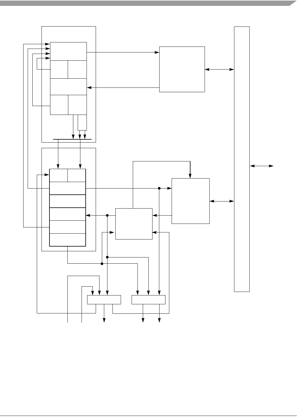
Features
MCF548x Reference Manual, Rev. 3
Freescale Semiconductor 3-3
Figure 3-1. ColdFire Enhanced Pipeline
3.2.1.1 Instruction Fetch Pipeline (IFP)
Because the fetch and execution pipelines are decoupled by a ten-instruction FIFO buffer, the IFP can
prefetch instructions before the OEP needs them, minimizing stalls.
Internal
IAG
IC1
IC2
IED
IB
DS
OAG
OC1
OC2
EX
DA
Branch
Cache
Branch
Accel.
PSTDDATADSODSCLK DSI
DDATA Debug
Instruction Fetch
Pipeline
Operand Execution
Pipeline
Instruction
Memory
Data
Misalignment
(Operand)
Memory
Module
PSTCLK
secDS
Bus

MCF548x Reference Manual, Rev. 3
3-4 Freescale Semiconductor
3.2.1.1.1 Branch Acceleration
To maximize the performance of conditional branch instructions, the IFP implements a sophisticated
two-level acceleration mechanism. The first level is an 8-entry, direct-mapped branch cache with 2 bits for
indicating four prediction states (strongly or weakly; taken or not-taken) for each entry. The branch cache
also provides the association between instruction addresses and the corresponding target address. In the
event of a branch cache hit, if the branch is predicted as taken, the branch cache sources the target address
from the IC1 stage back into the IAG to redirect the prefetch stream to the new location.
The branch cache implements instruction folding, so conditional branch instructions correctly predicted as
taken can execute in zero cycles. For conditional branches with no information in the branch cache, a
second-level, direct-mapped prediction table is accessed. Each of its 128 entries uses the same 2-bit
prediction mechanism as the branch cache.
If a branch is predicted as taken, branch acceleration logic in the IED stage generates the target address.
Other change-of-flow instructions, including unconditional branches, jumps, and subroutine calls, use a
similar mechanism where the IFP calculates the target address. The performance of subroutine return
instruction (RTS) is improved through the use of a four-entry, LIFO hardware return stack. In all cases,
these mechanisms allow the IFP to redirect the fetch stream down the predicted path well ahead of
instruction execution.
3.2.1.2 Operand Execution Pipeline (OEP)
The two instruction registers in the decode stage (DS) of the OEP are loaded from the FIFO instruction
buffer or are bypassed directly from the instruction early decode (IED). The OEP consists of two
traditional, two-stage RISC compute engines with a dual-ported register file access feeding an arithmetic
logic unit (ALU).
The compute engine at the top of the OEP (the address ALU) is used typically for operand address
calculations; the execution ALU at the bottom is used for instruction execution. The resulting structure
provides 4 Gbytes/S operand bandwidth (at 162 MHz) to the two compute engines and supports
single-cycle execution speeds for most instructions, including all load and store operations and most
embedded-load operations. The V4 OEP supports the ColdFire Revision B instruction set, which adds a
few new instructions to improve performance and code density.
The OEP also implements the following advanced performance features:
• Stalls are minimized by dynamically basing the choice between the address ALU or execution
ALU for instruction execution on the pipeline state.
• The address ALU and register renaming resources together can execute heavily used opcodes and
forward results to subsequent instructions with no pipeline stalls.
• Instruction folding involving MOVE instructions allows two instructions to be issued in one cycle.
The resulting microarchitecture approaches full superscalar performance at a much lower silicon
cost.
3.2.1.2.1 Illegal Opcode Handling
To aid in conversion from M68000 code, every 16-bit operation word is decoded to ensure that each
instruction is valid. If the processor attempts execution of an illegal or unsupported instruction, an illegal
instruction exception (vector 4) is taken.
3.2.1.2.2 Enhanced Multiply/Accumulate (EMAC) Unit
The EMAC unit in the Version 4e provides hardware support for a limited set of digital signal processing
(DSP) operations used in embedded code, while supporting the integer multiply instructions in the
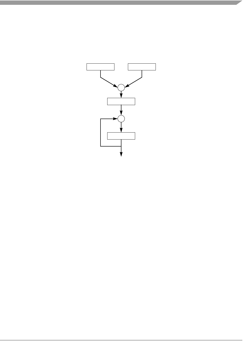
Features
MCF548x Reference Manual, Rev. 3
Freescale Semiconductor 3-5
ColdFire microprocessor family. The MAC features a four-stage execution pipeline, optimized for 32 × 32
multiplies. It is tightly coupled to the OEP, which can issue a 32 x 32 multiply with a 32-bit accumulation
and fetch a 32-bit operand in a single cycle. A 32 x 32 multiply with a 32-bit accumulation requires four
cycles before the next instruction can be issued.
Figure 3-2 shows basic functionality of the EMAC. A full set of instructions are provided for signed and
unsigned integers plus signed, fixed-point fractional input operands.
Figure 3-2. ColdFire Multiply-Accumulate Functionality Diagram
The EMAC provides functionality in the following three related areas, which are described in detail in
Chapter 4, “Enhanced Multiply-Accumulate Unit (EMAC):”
• Signed and unsigned integer multiplies
• Multiply-accumulate operations with signed and unsigned fractional operands
• Miscellaneous register operations
3.2.1.2.3 Memory Management Unit (MMU)
The ColdFire memory management architecture provides a demand-paged, virtual-address environment
with hardware address translation acceleration. It supports supervisor/user, read, write, and execute
permission checking on a per-memory request basis.
The architecture defines the MMU TLB, associated control logic, TLB hit/miss logic, address translation
based on the TLB contents, and access faults due to TLB misses and access violations. It intentionally
leaves some virtual environment details undefined to maximize the software-defined flexibility. These
include the exact structure of the memory-resident pointer descriptor/page descriptor tables, the base
registers for these tables, the exact information stored in the tables, the methodology (if any) for
maintenance of access, and written information on a per-page basis.
3.2.1.2.4 Floating Point Unit (FPU)
The floating-point unit (FPU) provides hardware support for floating point math operations. The FPU
conforms to the American National Standards Institute (ANSI)/Institute of Electrical and Electronics
Engineers (IEEE) Standard for Binary Floating-Point Arithmetic (ANSI/IEEE Standard 754).
X
+/-
Operand Y Operand X
Shift 0,1,-1
Accumulator

MCF548x Reference Manual, Rev. 3
3-6 Freescale Semiconductor
The hardware unit is optimized for real-time execution with exceptions disabled and default results
provided for specific operations, operands, and number types. The FPU does not support all IEEE-754
number types and operations in hardware. Exceptions can be enabled to support these cases in software.
3.2.1.2.5 Hardware Divide Unit
The hardware divide unit performs the following integer division operations:
• 32-bit operand/16-bit operand producing a 16-bit quotient and a 16-bit remainder
• 32-bit operand/32-bit operand producing a 32-bit quotient
• 32-bit operand/32-bit operand producing a 32-bit remainder
3.2.1.3 Harvard Memory Architecture
A Harvard memory architecture supports the increased bandwidth requirements of the CF4e processor
pipelines by providing separate configuration, access control, and protection resources for data (operand)
and instruction memory. The CF4e has separate instruction and data buses to processor-local memories,
eliminating conflicts between instruction fetches and operand accesses.
3.2.2 Debug Module Enhancements
The ColdFire processor core debug interface supports system integration in conjunction with low-cost
development tools. Real-time trace and debug information can be accessed through a standard interface,
which allows the processor and system to be debugged at full speed without costly in-circuit emulators.
The CF4e debug unit is a compatible upgrade to MCF52xx and MCF53xx debug modules with added
support for the CF4e MMU module.
The Version 2 ColdFire core implemented the original debug architecture, now called Revision A. Based
on feedback from customers and third-party developers, enhancements have been added to succeeding
generations of ColdFire cores. For Revision A, CSR[HRL] is 0. See Section 8.4.2, “Configuration/Status
Register (CSR).”
The Version 3 core implements Revision B of the debug architecture, offering more flexibility for
configuring the hardware breakpoint trigger registers and removing the restrictions involving concurrent
BDM processing while hardware breakpoint registers are active. For Revision B, CSR[HRL] is 1.
Revision C of the debug architecture more than doubles the on-chip breakpoint registers and provides an
ability to interrupt debug service routines. For Revision C, CSR[HRL] is 2.
Differences between Revision B and C are summarized as follows:
• Debug Revision B has separate PST[3:0] and DDATA[3:0] signals.
• Debug Revision C adds breakpoint registers and supports normal interrupt request service during
debug. It combines debug signals into PSTDDATA[7:0].
The addition of the memory management unit (MMU) to the baseline architecture requires corresponding
enhancements to the ColdFire debug functionality, resulting in Revision D. For Revision D, the revision
level bit, CSR[HRL], is 3.
With software support, the MMU can provide a demand-paged, virtual address environment. To support
debugging in this virtual environment, the debug enhancements are primarily related to the expansion of
the virtual address to include the 8-bit address space identifier (ASID). Conceptually, the virtual address
is expanded to a 40-bit value: the 8-bit ASID plus the 32-bit address.
The expansion of the virtual address affects the following two major debug functions:

Programming Model
MCF548x Reference Manual, Rev. 3
Freescale Semiconductor 3-7
• The ASID is optionally included in the specification of the hardware breakpoint registers. As an
example, the four PC breakpoint registers are each expanded by 8 bits, so that a specific ASID
value may be programmed as part of the breakpoint instruction address. Likewise, each operand
address/data breakpoint register is expanded to include an ASID value. Finally, new control
registers define if and how the ASID is to be included in the breakpoint comparison trigger logic.
• The debug module implements the concept of ownership trace in which the ASID value may be
optionally displayed as part of the real-time trace functionality. When enabled, real-time trace
displays instruction addresses on every change-of-flow instruction that is not absolute or
PC-relative. For Revision D, this instruction address display optionally includes the contents of the
ASID, thus providing the complete instruction virtual address on these instructions.
Additionally when a Sync_PC serial BDM command is loaded from the external development
system, the processor optionally displays the complete virtual instruction address, including the
8-bit ASID value.
In addition to these ASID-related changes, the new MMU control registers are accessible by using serial
BDM commands. The same BDM access capabilities are also provided for the EMAC and FPU
programming models.
Finally, a new serial BDM command is implemented to assist debugging when a software error generates
an incorrect memory address that hangs the external bus. The new BDM command attempts to break this
condition by forcing a bus termination.
3.3 Programming Model
The MCF548x programming model consists of two instruction and register groups—user and supervisor,
shown in Figure 3-3. User mode programs are restricted to user, EMAC, and floating point instructions
and programming models. Supervisor-mode system software can reference all user-mode, EMAC, and
floating point instructions and registers and additional supervisor instructions and control registers. The
user or supervisor programming model is selected based on SR[S]. The following sections describe the
registers in the user, EMAC, floating point, and supervisor programming models.
MCF548x Reference Manual, Rev. 3
3-8 Freescale Semiconductor
Figure 3-3. ColdFire Programming Model
31 0
D0 Data registers
D1
D2
D3
D4
D5
D6
D7
31 0
A0 Address registers
A1
A2
A3
A4
A5
A6
A7 User stack pointer
PC Program counter
CCR Condition code register
63 0
FP0 Floating-point data registers
FP1
FP2
FP3
FP4
FP5
FP6
FP7
FPCR Floating-point control register
FPSR Floating-point status register
FPIAR Floating-point instruction address register
31 0
MACSR MAC status register
ACC0 MAC accumulator 0
ACC1 MAC accumulator 1 (EMAC only)
ACC2 MAC accumulator 2 (EMAC only)
ACC3 MAC accumulator 3 (EMAC only)
ACCext01 ACC0 and ACC1 extensions
ACCext23 ACC2 and ACC3 extensions
MASK MAC mask register
15 0
31 19 (CCR) SR Status register
OTHER_A7 Supervisor A7 stack pointer
Must be zeros VBR Vector base register
CACR Cache control register
ASID Address space ID register
ACR0 Access control register 0 (data)
ACR1 Access control register 1 (data)
ACR2 Access control register 2 (instruction)
ACR3 Access control register 3 (instruction)
MMUBAR MMU base address register
ROMBAR0 ROM base address register 0
ROMBAR1 ROM base address register 1
RAMBAR0 RAM base address register0
RAMBAR1 RAM base address register 1
MBAR Module base address register
User Registers
Supervisor Registers

Programming Model
MCF548x Reference Manual, Rev. 3
Freescale Semiconductor 3-9
3.3.1 User Programming Model
The user programming model, shown in Figure 3-3, consists of the following registers:
• 16 general-purpose, 32-bit registers (D7–D0 and A7–A0); A7 is a user stack pointer
• 32-bit program counter
• 8-bit condition code register
• Registers to support the EMAC
• Register to support the floating-point unit (FPU)
3.3.1.1 Data Registers (D0–D7)
Registers D0–D7 are used as data registers for bit, byte (8-bit), word (16-bit), and longword (32-bit)
operations. They may also be used as index registers.
3.3.1.2 Address Registers (A0–A6)
The address registers (A0–A6) can be used as software stack pointers, index registers, or base address
registers, and may be used for word and longword operations.
3.3.2 User Stack Pointer (A7)
The CF4e architecture supports two unique stack pointer (A7) registers—the supervisor stack pointer
(SSP) and the user stack pointer (USP). This support provides the required isolation between operating
modes as dictated by the virtual memory management scheme provided by the memory management unit
(MMU). The SSP is described in Section 5.4.2, “Supervisor/User Stack Pointers.”
3.3.2.1 Program Counter (PC)
The PC holds the address of the executing instruction. For sequential instructions, the processor
automatically increments PC. When program flow changes, the PC is updated with the target instruction.
For some instructions, the PC specifies the base address for PC-relative operand addressing modes.
3.3.2.2 Condition Code Register (CCR)
The CCR, Figure 3-4, occupies SR[7–0], as shown in Figure 3-3. The CCR[4–0] bits are indicator flags
based on results generated by arithmetic operations.
7654 3210
R0 0 0 X N Z V C
W
Reset 0 0 0 0 0 0 0 0
Reg
Addr
Accessed using R/W commands for the status register
Figure 3-4. Condition Code Register (CCR)

MCF548x Reference Manual, Rev. 3
3-10 Freescale Semiconductor
3.3.3 EMAC Programming Model
The registers in the EMAC portion of the user programming model are described in Chapter 4, “Enhanced
Multiply-Accumulate Unit (EMAC),” and include the following registers:
• Four 48-bit accumulator registers partitioned as follows:
— Four 32-bit accumulators (ACC0–ACC3)
— Eight 8-bit accumulator extension bytes (two per accumulator). These are grouped into two
32-bit values for load and store operations (ACCEXT01 and ACCEXT23).
Accumulators and extension bytes can be loaded, copied, and stored, and results from EMAC
arithmetic operations generally affect the entire 48-bit destination.
• Eight 8-bit accumulator extensions (two per accumulator), packaged as two 32-bit values for load
and store operations (ACCext01 and ACCext23)
• One 16-bit mask register (MASK)
• One 32-bit status register (MACSR), including four indicator bits signaling product or
accumulation overflow (one for each accumulator: PAV0–PAV3).
These registers are shown in Figure 3-5.
Figure 3-5. EMAC Register Set
3.3.4 FPU Programming Model
The registers in the FPU portion of the programming model are described in Chapter 6, “Floating-Point
Unit (FPU),” and include the folllowing registers:
Table 3-1. CCR Field Descriptions
Bits Name Description
7–5 — Reserved, should be cleared.
4 X Extend condition code bit. Assigned the value of the carry bit for arithmetic operations;
otherwise not affected or set to a specified result. Also used as an input operand for
multiple-precision arithmetic.
3 N Negative condition code bit. Set if the msb of the result is set; otherwise cleared.
2 Z Zero condition code bit. Set if the result equals zero; otherwise cleared.
1 V Overflow condition code bit. Set if an arithmetic overflow occurs, implying that the result
cannot be represented in the operand size; otherwise cleared.
0 C Carry condition code bit. Set if a carry-out of the data operand msb occurs for an addition
or if a borrow occurs in a subtraction; otherwise cleared.
31 0
MACSR MAC status register
ACC0 MAC accumulator 0
ACC1 MAC accumulator 1
ACC2 MAC accumulator 2
ACC3 MAC accumulator 3
ACCext01 Extensions for ACC0 and ACC1
ACCext23 Extensions for ACC2 and ACC3
MASK MAC mask register

Programming Model
MCF548x Reference Manual, Rev. 3
Freescale Semiconductor 3-11
• Eight 64-bit floating-point data registers (FP0–FP7)
• One 32-bit floating-point control register (FPCR)
• One 32-bit floating-point status register (FPSR)
• One 32-bit floating-point instruction address register (FPIAR)
Figure 3-6 shows the FPU programming model.
Figure 3-6. Floating-Point Programmer’s Model
3.3.5 Supervisor Programming Model
The MCF548x supervisor programming model is shown in Figure 3-3. Typically, system programmers use
the supervisor programming model to implement operating system functions and provide memory and I/O
control. The supervisor programming model provides access to the user registers and additional supervisor
registers, which include the upper byte of the status register (SR), the vector base register (VBR), and
registers for configuring attributes of the address space connected to the Version 4 processor core. Most
supervisor-level registers are accessed by using the MOVEC instruction with the control register
definitions in Table 3-2.
63 31 0
FP0 Floating-point data registers
FP1
FP2
FP3
FP4
FP5
FP6
FP7
FPCR Floating-point control register
FPSR Floating-point status register
FPIAR Floating-point instruction address register
Table 3-2. MOVEC Register Map
Rc[11–0] Register Definition
0x002 Cache control register (CACR)
0x004 Access control register 0 (ACR0)
0x005 Access control register 1 (ACR1)
0x006 Access control register 2 (ACR2)
0x007 Access control register 3 (ACR3)
0x801 Vector base register (VBR)
0xC04 RAM base address register 0 (RAMBAR0)
0xC05 RAM base address register 1 (RAMBAR1)
0xC0F Module base address register (MBAR)

MCF548x Reference Manual, Rev. 3
3-12 Freescale Semiconductor
3.3.5.1 Status Register (SR)
The SR stores the processor status, the interrupt priority mask, and other control bits. Supervisor software
can read or write the entire SR; user software can read or write only SR[7–0], described in Section 3.3.2.2,
“Condition Code Register (CCR).” The control bits indicate processor states—trace mode (T), supervisor
or user mode (S), and master or interrupt state (M). SR is set to 0x27xx after reset.
Table 3-3 describes SR fields.
3.3.5.2 Vector Base Register (VBR)
The VBR holds the base address of the exception vector table in memory. The displacement of an
exception vector is added to the value in this register to access the vector table. The VBR[19–0] bits are
not implemented and are assumed to be zero, forcing the vector table to be aligned on a 0-modulo-1-Mbyte
boundary.
15 14 13 1211 10 9 8 7654 3 2 1 0
System byte Condition code register (CCR)
R T 0 S M 0 I 000X N Z V C
W
Reset0 0 100111000—————
Reg
Addr
0x27xx
Figure 3-7. Status Register (SR)
Table 3-3. SR Field Descriptions
Bits Name Description
15 T Trace enable. When T is set, the processor performs a trace exception after every
instruction.
13 S Supervisor/user state. Indicates whether the processor is in supervisor or user mode
0 User mode
1 Supervisor mode
12 M Master/interrupt state. Cleared by an interrupt exception. It can be set by software during
execution of the RTE or move to SR instructions so the OS can emulate an interrupt stack
pointer.
10–8 I Interrupt priority mask. Defines the current interrupt priority. Interrupt requests are inhibited
for all priority levels less than or equal to the current priority, except the edge-sensitive
level-7 request, which cannot be masked.
7–0 CCR Condition code register. See Table 3-1.

Programming Model
MCF548x Reference Manual, Rev. 3
Freescale Semiconductor 3-13
3.3.5.3 Cache Control Register (CACR)
The CACR controls operation of both the instruction and data cache memory. It includes bits for enabling,
freezing, and invalidating cache contents. It also includes bits for defining the default cache mode and
write-protect fields. See Section 7.10.1, “Cache Control Register (CACR).”
3.3.5.4 Access Control Registers (ACR0–ACR3)
The access control registers (ACR0–ACR3) define attributes for four user-defined memory regions: ACR0
and ACR1 control data memory space, and ACR2 and ACR3 control instruction memory space. Attributes
include definition of cache mode, write protect and buffer write enables. See Section 7.10.2, “Access
Control Registers (ACR0–ACR3).”
3.3.5.5 RAM Base Address Registers (RAMBAR0 and RAMBAR1)
The RAMBAR registers determine the base address location of the internal SRAM modules and indicate
the types of references mapped to each. Each RAMBAR includes a base address, write-protect bit, address
space mask bits, and an enable. The RAM base address must be aligned on a 0-module-2-Kbyte boundary.
See Section 7.4.1, “SRAM Base Address Registers (RAMBAR0/RAMBAR1).”
3.3.5.6 Module Base Address Register (MBAR)
The module base address register (MBAR) defines the logical base address for the memory-mapped space
containing the control registers for the on-chip peripherals. See Section 9.3.1, “Module Base Address
Register (MBAR).”
3.3.6 Programming Model Table
Table 3-4 lists register names, the CPU space location, whether the register is written from the processor
using the MOVEC instruction, and the complete register name.
31 30 29 28 27 26 25 24 23 22 21 20 19 18 17 16
R Exception vector table base address1000 0
W
Reset0 0 0000000000 0 0 0 0
Reg
Addr
0x801
15 14 13 12 11 10 9 8 7 6 5 4 3 2 1 0
R0 0 0000000000 0 0 0 0
W
Reset0 0 0000000000 0 0 0 0
Reg
Addr
0x801
1Written from a BDM serial command or from the CPU using the MOVEC instruction. VBR can be read from
the debug module only. The upper 12 bits are returned, the low-order 20 bits are undefined.
Figure 3-8. Vector Base Register (VBR)

MCF548x Reference Manual, Rev. 3
3-14 Freescale Semiconductor
Table 3-4. ColdFire CPU Registers
Name CPU Space (Rc) Written with MOVEC Register Name
Memory Management Control Registers
CACR 0x002 Yes Cache control register
ASID 0x003 Yes Address space identifier
ACR0–ACR3 0x004–0x007 Yes Access control registers 0–3
MMUBAR 0x008 Yes MMU base address register
Processor General-Purpose Registers
D0–D7 0x(0,1)80–0x(0,1
)87
No Data registers 0–7 (0 = load, 1 = store)
A0–A7 0x(0,1)88–0x(0,1
)8F
No Address registers 0–7 (0 = load, 1 = store) A7 is user
stack pointer
Processor Miscellaneous Registers
OTHER_A7 0x800 No Other stack pointer
VBR 0x801 Yes Vector base register
MACSR 0x804 No MAC status register
MASK 0x805 No MAC address mask register
ACC0–ACC3 0x806–0x80B No MAC accumulators 0–3
ACCext01 0x807 No MAC accumulator 0, 1 extension bytes
ACCext23 0x808 No MAC accumulator 2, 3 extension bytes
SR 0x80E No Status register
PC 0x80F Yes Program counter
Processor Floating-Point Registers
FPU0 0x810 No 32 msbs of floating-point data register 0
FPL0 0x811 No 32 lsbs of floating-point data register 0
FPU1 0x812 No 32 msbs of floating-point data register 1
FPL1 0x813 No 32 lsbs of floating-point data register 1
FPU2 0x814 No 32 msbs of floating-point data register 2
FPL2 0x815 No 32 lsbs of floating-point data register 2
FPU3 0x816 No 32 msbs of floating-point data register 3
FPL3 0x817 No 32 lsbs of floating-point data register 3
FPU4 0x818 No 32 msbs of floating-point data register 4
FPL4 0x819 No 32 lsbs of floating-point data register 4
FPU5 0x81A No 32 msbs of floating-point data register 5
FPL5 0x81B No 32 lsbs of floating-point data register 5
FPU6 0x81C No 32 msbs of floating-point data register 6

Data Format Summary
MCF548x Reference Manual, Rev. 3
Freescale Semiconductor 3-15
3.4 Data Format Summary
Table 3-5 lists the operand data formats. Integer operands can reside in registers, memory, or instructions.
The operand size is either explicitly encoded in the instruction or implicitly defined by the instruction
operation.
3.4.1 Data Organization in Registers
The following sections describe data organization in data, address, and control registers. Section 6.2.2,
“Floating-Point Data Formats,” describes floating-point formatting.
3.4.1.1 Integer Data Format Organization in Registers
Figure 3-9 shows the integer format for data registers. Each integer data register is 32 bits wide. Byte and
word operands occupy the lower 8- and 16-bit portions of integer data registers, respectively. Longword
operands occupy the entire 32 bits of integer data registers. A data register that is either a source or
destination operand only uses or changes the appropriate lower 8 or 16 bits in byte or word operations,
respectively. The remaining high-order portion does not change. Note that the least-significant bit is bit 0
for all data types, whereas the msbs for longword integer is bit 31, the msb of a word integer is bit 15, and
the msb of a byte integer is bit 7.
FPL6 0x81D No 32 lsbs of floating-point data register 6
FPU7 0x81E No 32 msbs of floating-point data register 7
FPL7 0x81F No 32 lsbs of floating-point data register 7
FPIAR 0x821 No Floating-point instruction address register
FPSR 0x822 No Floating-point status register
FPCR 0x824 No Floating-point control register
Local Memory and Module Control Registers
RAMBAR0 0xC04 Yes RAM base address register 0
RAMBAR1 0xC05 Yes RAM base address register 1
MBAR 0xC0F Yes Primary module base address register (not a core
register)
Table 3-5. Integer Data Formats
Operand Data Format Size
Bit 1 bit
Byte integer 8 bits
Word integer 16 bits
Longword integer 32 bits
Table 3-4. ColdFire CPU Registers (Continued)
Name CPU Space (Rc) Written with MOVEC Register Name

MCF548x Reference Manual, Rev. 3
3-16 Freescale Semiconductor
Instruction encodings disallow use of address registers for byte operands. When an address register is a
source operand, either the low-order word or the entire longword operand is used, depending on the
operation size. Word-length source operands are sign-extended to 32 bits and then used in the operation
with an address register destination. When an address register is a destination, the entire register is
affected, regardless of the operation size. Figure 3-10 shows integer formats for address registers.
The size of control registers varies according to function. Some have undefined bits reserved for future
definition by Freescale. Those bits read as zeros and must be written as zeros for future compatibility.
Operations to the SR and CCR are word-sized. The upper CCR byte is read as all zeros and is ignored when
written, regardless of privilege mode.
3.4.1.2 Integer Data Format Organization in Memory
ColdFire processors use big-endian addressing. Byte-addressable memory organization allows lower
addresses to correspond to higher-order bytes. The address N of a longword data item corresponds to the
address of the high-order word. The lower-order word is at address N + 2. The address of a word data item
corresponds to the address of the high-order byte. The lower-order byte is at address N + 1. This
organization is shown in Figure 3-11.
31 30 1 0
msb lsb Bit (0 bit number 31)
31 8 7 6 1 0
Not used msb Lower-order byte lsb Byte (8 bits)
31 16 15 14 1 0
Not used msb Lower-order word lsb Word (16 bits)
31 30 1 0
msb Longword lsb Longword (32 bits)
Figure 3-9. Organization of Integer Data Format in Data Registers
31 16 15 0
Sign-Extended 16-Bit Address Operand
31 0
Full 32-Bit Address Operand
Figure 3-10. Organization of Integer Data Formats in Address Registers

Data Format Summary
MCF548x Reference Manual, Rev. 3
Freescale Semiconductor 3-17
3.4.2 EMAC Data Representation
The EMAC supports the following three modes, where each mode defines a unique operand type.
• Two’s complement signed integer: In this format, an N-bit operand value lies in the range -2(N-1)
< operand < 2(N-1) - 1. The binary point is right of the lsb.
• Unsigned integer: In this format, an N-bit operand value lies in the range 0 < operand < 2N - 1. The
binary point is right of the lsb.
• Two’s complement, signed fractional: In an N-bit number, the first bit is the sign bit. The remaining
bits signify the first N-1 bits after the binary point. Given an N-bit number, aN-1aN-2aN-3... a2a1a0,
its value is given by the equation in Figure 3-12.
Figure 3-12. Two’s Complement, Signed Fractional Equation
This format can represent numbers in the range -1 < operand < 1 - 2(N-1).
For words and longwords, the largest negative number that can be represented is -1, whose internal
representation is 0x8000 and 0x8000_0000, respectively. The largest positive word is 0x7FFF or (1 – 2-15);
the most positive longword is 0x7FFF_FFFF or (1 – 2-31).
For more information, see Chapter 4, “Enhanced Multiply-Accumulate Unit (EMAC).”
3.4.2.1 Floating-Point Data Formats and Types
The FPU supports signed byte, word, and longword integer formats, which are identical to those
supported by the integer unit. The FPU also supports single- and double-precision binary
floating-point formats that fully comply with the IEEE-754 standard.
For more information, see Chapter 6, “Floating-Point Unit (FPU).”
31 24 23 16 15 8 7 0
Longword 0x0000_0000
Word 0x0000_0000 Word 0x0000_0002
Byte 0x0000_0000 Byte 0x0000_0001 Byte 0x0000_0002 Byte 0x0000_0003
Longword 0x0000_0004
Word 0x0000_0004 Word 0x0000_0006
Byte 0x0000_0004 Byte 0x0000_0005 Byte 0x0000_0006 Byte 0x0000_0007
...
...
...
Longword 0xFFFF_FFFC
Word 0xFFFF_FFFC Word 0xFFFF_FFFE
Byte 0xFFFF_FFFC Byte 0xFFFF_FFFD Byte 0xFFFF_FFFE Byte 0xFFFF_FFFF
Figure 3-11. Memory Operand Addressing
value 1 aN1–
⋅()–2
i1N–+()
ai⋅
i0=
N2–
∑
+=
MCF548x Reference Manual, Rev. 3
3-18 Freescale Semiconductor
3.4.2.1.1 Signed-Integer Data Formats
The FPU supports 8-bit byte (B), 16-bit word (W), and 32-bit longword (L) integer data formats.
3.4.2.1.2 Floating-Point Data Formats
Figure 3-13 shows the two binary floating-point data formats.
Figure 3-13. Floating-Point Data Formats
Note that, throughout this chapter, a mantissa is defined as the concatenation of an integer bit, the binary
point, and a fraction. A fraction is the term designating the bits to the right of the binary point in the
mantissa.
Figure 3-14. Mantissa
The integer bit is implied to be set for normalized numbers and infinities, clear for zeros and denormalized
numbers. For not-a-numbers (NANs), the integer bit is ignored. The exponent in both floating-point
formats is an unsigned binary integer with an implied bias added to it. Subtracting the bias from exponent
yields a signed, two’s complement power of two. This represents the magnitude of a normalized
floating-point number when multiplied by the mantissa.
By definition, a normalized mantissa always takes values starting from 1.0 and going up to, but not
including, 2.0; that is, [1.0...2.0).
3.5 Addressing Mode Summary
Addressing modes are categorized by how they are used. Data addressing modes refer to data operands.
Memory addressing modes refer to memory operands. Alterable addressing modes refer to alterable
(writable) data operands. Control addressing modes refer to memory operands without an associated size.
These categories sometimes combine to form more restrictive categories. Two combined classifications
are alterable memory (both alterable and memory) and data alterable (both alterable and data). Twelve of
the most commonly used effective addressing modes from the M68000 Family are available on ColdFire
microprocessors. Table 3-6 summarizes these modes and their categories.
11-Bit Exponent
S52-Bit Fraction
62 51 0
Sign of Mantissa
0
23-Bit Fraction8-Bit Exponent
S
Sign of Mantissa
2230
Single
Double
31
63
(integer bit).(fraction)
Mantissa

Instruction Set Summary
MCF548x Reference Manual, Rev. 3
Freescale Semiconductor 3-19
3.6 Instruction Set Summary
The ColdFire instruction set is a simplified version of the M68000 instruction set. The removed
instructions include BCD, bit field, logical rotate, decrement and branch, and integer multiply with a 64-bit
result.
“About This Book” lists notational conventions used throughout this manual.
3.6.1 Additions to the Instruction Set Architecture
The original ColdFire ISA was derived from M68000 Family opcodes based on extensive analysis of
embedded application code. After the first ColdFire compilers were created, developers identified ISA
additions that would enhance both code density and overall performance. Additionally, as users
implemented ColdFire-based designs into a wide range of embedded systems, they identified frequently
used instruction sequences that could be improved by creating new instructions. This observation was
especially prevalent in environments that used substantial amounts of assembly language code.
The original ISA minimized support for instructions referencing byte and word operands. MOVE.B and
MOVE.W were fully supported; otherwise, only CLR (clear) and TST (test) supported these data types.
Based on input from compiler writers and system users, a set of instruction enhancements was proposed
to address the following:
Table 3-6. ColdFire Effective Addressing Modes
Addressing Modes Syntax Mode
Field
Reg.
Field
Category
Data Memory Control Alterable
Register direct
Data
Address
Dn
An
000
001
reg. no.
reg. no.
X
—
—
—
—
—
X
X
Register indirect
Address
Address with
Postincrement
Address with
Predecrement
Address with
Displacement
(An)
(An)+
–(An)
(d16, An)
010
011
100
101
reg. no.
reg. no.
reg. no.
reg. no.
X
X
X
X
X
X
X
X
X
—
—
X
X
X
X
X
Address register indirect with
scaled index
8-bit displacement
(d8, An,
Xi*SF)
110 reg. no. X X X X
Program counter indirect
with displacement (d16, PC) 111 010 X X X —
Program counter indirect with
scaled index
8-bit displacement
(d8, PC,
Xi*SF)
111 011 X X X —
Absolute data addressing
Short
Long
(xxx).W
(xxx).L
111
111
000
001
X
X
X
X
X
X
—
—
Immediate #<xxx> 111 100 X X — —

MCF548x Reference Manual, Rev. 3
3-20 Freescale Semiconductor
• Enhanced support for byte and word-sized operands through new move operations
• Enhanced support for position-independent code
For descriptions of the ColdFire instruction set, see the latest version of the ColdFire Programmer’s
Reference Manual.
The following list summarizes new and enhanced instructions of ISA_B:
• New instructions:
— INTOUCH loads blocks of instructions to be locked in the instruction cache.
— MOV3Q.L moves 3-bit immediate data to the destination location.
— MOVE to/from USP loads and stores user stack pointer.
— MVS.{B,W} sign-extends the source operand and moves it to the destination register.
— MVZ.{B,W} zero-fills the source operand and moves it to the destination register.
— SATS.L performs a saturation operation for signed arithmetic and updates the destination
register depending on CCR[V] and bit 31 of the register.
— TAS.B performs an indivisible read-modify-write cycle to test and set the addressed memory
byte.
• Enhancements to existing Revision_A instructions:
— Longword support for branch instructions (Bcc, BRA, BSR)
— Byte and word support for compare instructions (CMP, CMPI)
— Word support for the compare address register instruction (CMPA)
— Byte and longword support for MOVE.x,where the source is immediate data and the
destination is specified by d16(Ax); that is, MOVE.{B,W} #<data>, d16(Ax)
• Floating-point instructions. See Chapter 6, “Floating-Point Unit (FPU).”
• EMAC instructions. See Chapter 4, “Enhanced Multiply-Accumulate Unit (EMAC),” for more
information.
Table 3-7 shows the syntax for the new and enhanced instructions. As Table 3-7 shows, some ISA_B
opcodes were defined in the M68000 family and others are new.
Table 3-7. V4 New Instruction Summary
Instruction Mnemonic1Source Destination M68000
ISA_B Extensions
Branch Always bra.l <label> Yes
Branch Conditionally bcc.l <label> Yes
Branch to Subroutine bsr.l <label> Yes
Compare cmp.{b,w,l} <ea>y Dx Yes
Compare Address cmpa.w <ea>y Ax Yes
Compare Immediate cmpi.{b,w} #<data> Dx Yes
Instruction Fetch Touch intouch <Ay>
Move 3-Bit Data Quick mov3q.l #<data> <ea>x
Move Data Source to Destination move.{b,w} #<data> d16(Ax) Yes
Move from USP move.l USP Ax Yes

Instruction Set Summary
MCF548x Reference Manual, Rev. 3
Freescale Semiconductor 3-21
Move to USP move.l Ay USP Yes
Move with Sign Extend mvs.{b,w} <ea>y Dx
Move with Zero-Fill mvz.{b,w} <ea>y Dx
Signed Saturate sats.l Dx
Test and Set an Operand tas.b <ea>x Yes
EMAC Extensions
Move from an Accumulator and Clear movclr.l ACCx Rx No
Copy an Accumulator move.l ACCy ACCx No
Move from Accumulator 0 and 1 Extensions move.l ACCext01 Rx No
Move from Accumulator 2 and 3 Extensions move.l ACCext23 Rx No
Move to Accumulator 0 and 1 Extensions move.l Ry ACCext01 No
Move to Accumulator 2 and 2 Extensions move.l Ry ACCext23 No
FPU Instructions
Floating-Point Absolute Value fabs.{b,w,l,s,d} <ea>y FPx Yes
Floating-Point Add fadd.{b,w,l,s,d} <ea>y FPx Yes
Floating-Point Branch Conditionally fbcc.{w,l} <label> Yes
Floating-Point Compare fcmp.{b,w,l,s,d} <ea>y FPx Yes
Floating-Point Divide fdiv.{b,w,l,s,d} <ea>y FPx Yes
Floating-Point Integer fint.{b,w,l,s,d} <ea>y FPx Yes
Floating-Point Integer Round-to-Zero fintrz.{b,w,l,s,d} <ea>y FPx Yes
Move Floating-Point Data Register fmove.{b,w,l,s,d} <ea>y FPx Yes
Move from FPCR fmove.l FPCR <ea>x Yes
Move from FPIAR fmove.l FPIAR <ea>x Yes
Move from FPSR fmove.l FPSR <ea>x Yes
Move from FPCR fmove.l <ea>y FPCR Yes
Move from FPIAR fmove.l <ea>y FPIAR Yes
Move from FPSR fmove.l <ea>y FPSR Yes
Move Multiple Floating Point Data Registers fmovem.d #list
<ea>y
<ea>x
#list
Yes
Floating-Point Multiply fmul.{b,w,l,s,d} <ea>y FPx Yes
Floating-Point Negate fneg.{b,w,l,s,d} <ea>y FPx Yes
Floating-Point No Operation fnop Yes
Restore Internal Floating Point State frestore <ea>y Yes
Table 3-7. V4 New Instruction Summary (Continued)
Instruction Mnemonic1Source Destination M68000

MCF548x Reference Manual, Rev. 3
3-22 Freescale Semiconductor
3.6.2 Instruction Set Summary
Table 3-8 lists user-mode instructions by opcode.
Save Internal Floating Point State fsave <ea>x Yes
Floating-Point Square Root fsqrt.{b,w,l,s,d} <ea>y FPx Yes
Floating-Point Subtract fsub.{b,w,l,s,d} <ea>y FPx Yes
Test Floating-Point Operand ftst.{b,w,l,s,d} <ea>y Yes
1Operand sizes in this column reflect only newly supported operand sizes for existing instructions (Bcc, BRA,
BSR, CMP, CMPA, CMPI, and MOVE)
Table 3-8. User-Mode Instruction Set Summary
Instruction Operand Syntax Operand Size Operation
ADD
ADDA
Dy,<ea>x
<ea>y,Dx
<ea>y,Ax
L
L
L
Source + Destination → Destination
ADDI
ADDQ
#<data>,Dx
#<data>,<ea>x
L
L
Immediate Data + Destination → Destination
ADDX Dy,Dx L Source + Destination + CCR[X] → Destination
AND <ea>y,Dx
Dy,<ea>x
L
L
Source & Destination → Destination
ANDI #<data>, Dx L Immediate Data & Destination → Destination
ASL Dy,Dx
#<data>,Dx
L
L
CCR[X,C] ← (Dx << Dy) ← 0
CCR[X,C] ← (Dx << #<data>) ← 0
ASR Dy,Dx
#<data>,Dx
L
L
msb → (Dx >> Dy) → CCR[X,C]
msb → (Dx >> #<data>) → CCR[X,C
Bcc <label> B, W, L If Condition True, Then PC + dn → PC
BCHG Dy,<ea>x
#<data>,<ea>x
B, L
B, L
~ (<bit number> of Destination) → CCR[Z] →
<bit number> of Destination
BCLR Dy,<ea>x
#<data>,<ea>x
B, L
B, L
~ (<bit number> of Destination) → CCR[Z];
0 →<bit number> of Destination
BRA <label> B, W, L PC + dn → PC
BSET Dy,<ea>x
#<data>,<ea>x
B, L
B, L
~ (<bit number> of Destination) → CCR[Z];
1 → <bit number> of Destination
BSR <label> B, W, L SP – 4 → SP; nextPC → (SP); PC + dn → PC
BTST Dy,<ea>x
#<data>,<ea>x
B, L
B, L
~ (<bit number> of Destination) → CCR[Z]
CLR <ea>x B, W, L 0 → Destination
Table 3-7. V4 New Instruction Summary (Continued)
Instruction Mnemonic1Source Destination M68000

Instruction Set Summary
MCF548x Reference Manual, Rev. 3
Freescale Semiconductor 3-23
CMP
CMPA
<ea>y,Dx
<ea>y,Ax
B, W, L
W, L
Destination – Source → CCR
CMPI #<data>,Dx B, W, L Destination – Immediate Data → CCR
DIVS/DIVU <ea>y,Dx W, L Destination / Source → Destination
(Signed or Unsigned)
EOR Dy,<ea>x L Source ^ Destination → Destination
EORI #<data>,Dx L Immediate Data ^ Destination → Destination
EXT
EXTB
Dx
Dx
Dx
B → W
W → L
B → L
Sign-Extended Destination → Destination
FABS <ea>y,FPx
FPy,FPx
FPx
B,W,L,S,D
D
D
Absolute Value of Source → FPx
Absolute Value of FPx → FPx
FADD <ea>y,FPx
FPy,FPx
B,W,L,S,D
D
Source + FPx → FPx
FBcc <label> W, L If Condition True, Then PC + dn → PC
FCMP <ea>y,FPx
FPy,FPx
B,W,L,S,D
D
FPx - Source
FDABS <ea>y,FPx
FPy,FPx
FPx
B,W,L,S,D
D
D
Absolute Value of Source → FPx; round destination
to double
Absolute Value of FPx → FPx; round destination to
double
FDADD <ea>y,FPx
FPy,FPx
B,W,L,S,D
D
Source + FPx → FPx; round destination to double
FDDIV <ea>y,FPx
FPy,FPx
B,W,L,S,D
D
FPx / Source → FPx; round destination to double
FDIV <ea>y,FPx
FPy,FPx
B,W,L,S,D
D
FPx / Source → FPx
FDMOVE FPy,FPx D Source → Destination; round destination to double
FDMUL <ea>y,FPx
FPy,FPx
B,W,L,S,D
D
Source * FPx → FPx; round destination to double
FDNEG <ea>y,FPx
FPy,FPx
FPx
B,W,L,S,D
D
D
- (Source) → FPx; round destination to double
- (FPx) → FPx; round destination to double
FDSQRT <ea>y,FPx
FPy,FPx
FPx
B,W,L,S,D
D
D
Square Root of Source → FPx; round destination to
double
Square Root of FPx → FPx; round destination to
double
FDSUB <ea>y,FPx
FPy,FPx
B,W,L,S,D
D
FPx - Source → FPx; round destination to double
Table 3-8. User-Mode Instruction Set Summary (Continued)
Instruction Operand Syntax Operand Size Operation

MCF548x Reference Manual, Rev. 3
3-24 Freescale Semiconductor
FINT <ea>y,FPx
FPy,FPx
FPx
B,W,L,S,D
D
D
Integer Part of Source → FPx
Integer Part of FPx → FPx
FINTRZ <ea>y,FPx
FPy,FPx
FPx
B,W,L,S,D
D
D
Integer Part of Source → FPx; round to zero
Integer Part of FPx → FPx; round to zero
FMOVE <ea>y,FPx
FPy,<ea>x
FPy,FPx
FPcr,<ea>x
<ea>y,FPcr
B,W,L,S,D
B,W,L,S,D
D
L
L
Source → Destination
FPcr can be any floating point control register:
FPCR, FPIAR, FPSR
FMOVEM #list,<ea>x
<ea>y,#list
D Listed registers → Destination
Source → Listed registers
FMUL <ea>y,FPx
FPy,FPx
B,W,L,S,D
D
Source * FPx → FPx
FNEG <ea>y,FPx
FPy,FPx
FPx
B,W,L,S,D
D
D
- (Source) → FPx
- (FPx) → FPx
FNOP none none PC + 2 → PC (FPU Pipeline Synchronized)
FSABS <ea>y,FPx
FPy,FPx
FPx
B,W,L,S,D
D
D
Absolute Value of Source → FPx; round destination
to single
Absolute Value of FPx → FPx; round destination to
single
FSADD <ea>y,FPx
FPy,FPx
B,W,L,S,D Source + FPx → FPx; round destination to single
FSDIV <ea>y,FPx
FPy,FPx
B,W,L,S,D
D
FPx / Source → FPx; round destination to single
FSMOVE <ea>y,FPx B,W,L,S,D Source → Destination; round destination to single
FSMUL <ea>y,FPx
FPy,FPx
B,W,L,S,D
D
Source * FPx → FPx; round destination to single
FSNEG <ea>y,FPx
FPy,FPx
FPx
B,W,L,S,D
D
D
- (Source) → FPx; round destination to single
- (FPx) → FPx; round destination to single
FSQRT <ea>y,FPx
FPy,FPx
FPx
B,W,L,S,D
D
D
Square Root of Source → FPx
Square Root of FPx → FPx
FSSQRT <ea>y,FPx
FPy,FPx
FPx
B,W,L,S,D
D
D
Square Root of Source → FPx; round destination to
single
Square Root of FPx → FPx; round destination to
single
FSSUB <ea>y,FPx
FPy,FPx
B,W,L,S,D
D
FPx - Source → FPx; round destination to single
Table 3-8. User-Mode Instruction Set Summary (Continued)
Instruction Operand Syntax Operand Size Operation

Instruction Set Summary
MCF548x Reference Manual, Rev. 3
Freescale Semiconductor 3-25
FSUB <ea>y,FPx
FPy,FPx
B,W,L,S,D
D
FPx - Source → FPx
FTST <ea>y B, W, L, S, D Source Operand Tested → FPCC
ILLEGAL none none SP – 4 → SP; PC → (SP) → PC; SP – 2 → SP;
SR → (SP); SP – 2 → SP; Vector Offset → (SP);
(VBR + 0x10) → PC
JMP <ea>y none Source Address → PC
JSR <ea>y none SP – 4 → SP; nextPC → (SP); Source → PC
LEA <ea>y,Ax L <ea>y → Ax
LINK Ay,#<displacement> W SP – 4 → SP; Ay → (SP); SP → Ay, SP + dn → SP
LSL Dy,Dx
#<data>,Dx
L
L
CCR[X,C] ← (Dx << Dy) ← 0
CCR[X,C] ← (Dx << #<data>) ← 0
LSR Dy,Dx
#<data>,Dx
L
L
0 → (Dx >> Dy) → CCR[X,C]
0 → (Dx >> #<data>) → CCR[X,C]
MAC Ry,RxSF,ACCx
Ry,RxSF,<ea>y,Rw,ACCx
W, L
W, L
ACCx + (Ry * Rx){<<|>>}SF → ACCx
ACCx + (Ry * Rx){<<|>>}SF → ACCx;
(<ea>y(&MASK)) → Rw
MOV3Q #<data>,<ea>x L Immediate Data → Destination
MOVCLR ACCy,Rx L Accumulator → Destination, 0 → Accumulator
MOVE
MOVE from
CCR
MOVE to CCR
<ea>y,<ea>x
MACcr,Dx
<ea>y,MACcr
CCR,Dx
<ea>y,CCR
B,W,L
L
L
W
W
Source → Destination
where MACcr can be any MAC control register:
ACCx, ACCext01, ACCext23, MACSR, MASK
MOVEA <ea>y,Ax W,L → L Source → Destination
MOVEM #list,<ea>x
<ea>y,#list
L Listed Registers → Destination
Source → Listed Registers
MOVEQ #<data>,Dx B → L Immediate Data → Destination
MSAC Ry,RxSF,ACCx
Ry,RxSF,<ea>y,Rw,ACCx
W, L
W, L
ACCx - (Ry * Rx){<<|>>}SF → ACCx
ACCx - (Ry * Rx){<<|>>}SF → ACCx;
(<ea>y(&MASK)) → Rw
MULS/MULU <ea>y,Dx W * W → L
L * L → L
Source * Destination → Destination
(Signed or Unsigned)
MVS <ea>y,Dx B,W Source with sign extension → Destination
MVZ <ea>y,Dx B,W Source with zero fill → Destination
NEG Dx L 0 – Destination → Destination
NEGX Dx L 0 – Destination – CCR[X] → Destination
NOP none none PC + 2 → PC (Integer Pipeline Synchronized)
Table 3-8. User-Mode Instruction Set Summary (Continued)
Instruction Operand Syntax Operand Size Operation

MCF548x Reference Manual, Rev. 3
3-26 Freescale Semiconductor
Table 3-9 describes supervisor-mode instructions.
NOT Dx L ~ Destination → Destination
OR <ea>y,Dx
Dy,<ea>x
L
L
Source | Destination → Destination
ORI #<data>,Dx L Immediate Data | Destination → Destination
PEA <ea>y L SP – 4 → SP; <ea>y → (SP)
PULSE none none Set PST = 0x4
REMS/REMU <ea>y,Dw:Dx L Destination / Source → Remainder
(Signed or Unsigned)
RTS none none (SP) → PC; SP + 4 → SP
SATS Dx L If CCR[V] == 1;
then if Dx[31] == 0;
then Dx[31:0] = 0x80000000;
else Dx[31:0] = 0x7FFFFFFF;
else Dx[31:0] is unchanged
Scc Dx B If Condition True, Then 1s → Destination;
Else 0s → Destination
SUB
SUBA
<ea>y,Dx
Dy,<ea>x
<ea>y,Ax
L
L
L
Destination - Source → Destination
SUBI
SUBQ
#<data>,Dx
#<data>,<ea>x
L
L
Destination – Immediate Data → Destination
SUBX Dy,Dx L Destination – Source – CCR[X] → Destination
SWAP Dx W MSW of Dx ↔ LSW of Dx
TAS <ea>x B Destination Tested → CCR;
1 → bit 7 of Destination
TPF none
#<data>
#<data>
none
W
L
PC + 2→ PC
PC + 4 → PC
PC + 6→ PC
TRAP #<vector> none 1 → S Bit of SR; SP – 4 → SP; nextPC → (SP);
SP – 2 → SP; SR → (SP)
SP – 2 → SP; Format/Offset → (SP)
(VBR + 0x80 +4*n) → PC, where n is the TRAP
number
TST <ea>y B, W, L Source Operand Tested → CCR
UNLK Ax none Ax → SP; (SP) → Ax; SP + 4 → SP
WDDATA <ea>y B, W, L Source → DDATA port
Table 3-8. User-Mode Instruction Set Summary (Continued)
Instruction Operand Syntax Operand Size Operation

Instruction Execution Timing
MCF548x Reference Manual, Rev. 3
Freescale Semiconductor 3-27
3.7 Instruction Execution Timing
The timing data in this section assumes the following:
• Execution times for individual instructions make no assumptions concerning the OEP’s ability to
dispatch multiple instructions in one machine cycle. For sequences where instruction pairs are
issued, the execution time of the first instruction defines the execution time of pair; the second
instruction effectively executes in zero cycles.
• The OEP is loaded with the opword and all required extension words at the beginning of each
instruction execution. This implies that the OEP spends no time waiting for the IFP to supply
opwords or extension words.
• The OEP experiences no sequence-related pipeline stalls. For the V4, the most common example
of this type of stall occurs when a register is modified in the EX engine and a subsequent instruction
generates an address that uses the previously modified register. The second instruction stalls in the
OEP until the previous instruction updates the register. For example:
muls.l #<data>,d0
move.l (a0,d0.l*4),d1
move.l waits 3 cycles for the muls.l to update d0. If consecutive instructions update a register and
use that register as a base of index value with a scale factor of 1 (Xi.l*1) in an address calculation,
a 2-cycle pipeline stall occurs. If the destination register is used as an index register with any other
scale factor (Xi.l*2, Xi.l*4), a 3-cycle stall occurs.
NOTE
Address register results from postincrement and predecrement modes are
available to subsequent instructions without stalls.
Table 3-9. Supervisor-Mode Instruction Set Summary
Instruction Operand Syntax Operand Size Operation
CPUSHL ic,(Ax)
dc,(Ax)
bc,(Ax)
none If data is valid and modified, push cache line; invalidate line
if programmed in CACR (synchronizes pipeline)
FRESTORE <ea>y none FPU State Frame → Internal FPU State
FSAVE <ea>x none Internal FPU State → FPU State Frame
HALT none none Halt processor core
INTOUCH Ay none Instruction fetch touch at (Ay)
MOVE from SR SR,Dx W SR → Destination
MOVE from USP USP,Dx L USP → Destination
MOVE to SR <ea>y,SR W Source → SR; Dy or #<data> source only
MOVE to USP Ay,USP L Source → USP
MOVEC Ry,Rc L Ry → Rc
RTE none none 2 (SP) → SR; 4 (SP) → PC; SP + 8 →SP
Adjust stack according to format
STOP #<data> none Immediate Data → SR; STOP
WDEBUG <ea>y L Addressed Debug WDMREG Command Executed

MCF548x Reference Manual, Rev. 3
3-28 Freescale Semiconductor
• The OEP can complete all memory accesses without memory causing any stalls. Thus, these
timings assume an infinite, zero-wait state memory attached to the core.
• Operand accesses are assumed to be aligned as follows:
— 16-bit operands are aligned on 0-modulo-2 addresses
— 32-bit operands are aligned on 0-modulo-4 addresses
Operands that do not meet these guidelines are misaligned. Table 3-10 shows how the core
decomposes a misaligned operand reference into a series of aligned accesses.
3.7.1 MOVE Instruction Execution Timing
The following tables show execution times for the MOVE.{B,W,L} instructions. Table 3-13 shows the
timing for the other generic move operations.
NOTE
In these tables, times using PC-relative effective addressing modes are the
same as using An-relative mode.
The (xxx).wl nomenclature refers to both forms of absolute addressing,
(xxx).w and (xxx).l.
Table 3-11 lists execution times for MOVE.{B,W} instructions.
Table 3-10. Misaligned Operand References
A[1:0] Size Bus Operations Additional C(R/W)1
1Each timing entry is presented as C(r/w), described as follows:
C is the number of processor clock cycles, including all applicable operand fetches and writes, as well as all
internal core cycles required to complete the instruction execution.
r/w is the number of operand reads (r) and writes (w) required by the instruction. An operation performing a
read-modify write function is denoted as (1/1).
x1 Word Byte, Byte 2(1/0) if read
1(0/1) if write
x1 Long Byte, Word, Byte 3(2/0) if read
2(0/2) if write
10 Long Word, Word 2(1/0) if read
1(0/1) if write
ET with {<ea> = (d16,PC)} equals ET with {<ea> = (d16,An)}
ET with {<ea> = (d8,PC,Xi*SF)} equals ET with {<ea> = (d8,An,Xi*SF)}
Table 3-11. Move Byte and Word Execution Times
Source
Destination
Rx (Ax) (Ax)+ –(Ax) (d16,Ax) (d8,Ax,Xi*SF) (xxx).wl
Dy 1(0/0) 1(0/1) 1(0/1) 1(0/1) 1(0/1) 2(0/1) 1(0/1)
Ay 1(0/0) 1(0/1) 1(0/1) 1(0/1) 1(0/1) 2(0/1) 1(0/1)
(Ay) 1(1/0) 2(1/1) 2(1/1) 2(1/1) 2(1/1) 3(1/1) 2(1/1)

Instruction Execution Timing
MCF548x Reference Manual, Rev. 3
Freescale Semiconductor 3-29
Table 3-12 lists timings for MOVE.L.
Table 3-13 gives timings for MOVE.L instructions accessing program-visible EMAC registers, along with
other MOVE.L timings. Execution times for moving ACC or MACSR contents into a destination location
represent the best-case scenario when the store instruction is executed and no load, MAC, or MSAC
instructions are in the EMAC execution pipeline. In general, these store operations take only 1 cycle to
execute, but if preceded immediately by a load, MAC, or MSAC instruction, the EMAC pipeline depth is
exposed and execution time is 3 cycles.
Table 3-19 lists EMAC execution times.
(Ay)+ 1(1/0) 2(1/1) 2(1/1) 2(1/1) 2(1/1) 3(1/1) 2(1/1)
-(Ay) 1(1/0) 21/1) 2(1/1) 2(1/1) 2(1/1) 3(1/1) 2(1/1)
(d16,Ay) 1(1/0) 2(1/1) 2(1/1) 2(1/1) 2(1/1) — —
(d8,Ay,Xi*SF) 2(1/0) 3(1/1) 3(1/1) 3(1/1) — — —
(xxx).w 1(1/0) 2(1/1) 2(1/1) 2(1/1) — — —
(xxx).l 1(1/0) 2(1/1) 2(1/1) 2(1/1) — — —
(d16,PC) 1(1/0) 2(1/1) 2(1/1) 2(1/1) 2(1/1) — —
(d8,PC,Xi*SF) 2(1/0) 3(1/1) 3(1/1) 3(1/1) — — —
#<xxx> 1(0/0) 1(0/1) 1(0/1) 1(0/1) 1(0/1) — —
Table 3-12. Move Long Execution Times
Source
Destination
Rx (Ax) (Ax)+ –(Ax) (d16,Ax) (d8,Ax,Xi*SF) (xxx).wl
Dy 1(0/0) 1(0/1) 1(0/1) 1(0/1) 1(0/1) 2(0/1) 1(0/1)
Ay 1(0/0) 1(0/1) 1(0/1) 1(0/1) 1(0/1) 2(0/1) 1(0/1)
(Ay) 1(1/0) 2(1/1) 2(1/1) 2(1/1) 2(1/1) 3(1/1) 2(1/1)
(Ay)+ 1(1/0) 2(1/1) 2(1/1) 2(1/1) 2(1/1) 3(1/1) 2(1/1)
-(Ay) 1(1/0) 2(1/1) 2(1/1) 2(1/1) 2(1/1) 3(1/1) 2(1/1)
(d16,Ay) 1(1/0) 2(1/1) 2(1/1) 2(1/1) 2(1/1) — —
(d8,Ay,Xi*SF) 2(1/0) 3(1/1) 3(1/1) 3(1/1) — — —
(xxx).w 1(1/0) 2(1/1) 2(1/1) 2(1/1) — — —
(xxx).l 1(1/0) 2(1/1) 2(1/1) 2(1/1) — — —
(d16,PC) 1(1/0) 2(1/1) 2(1/1) 2(1/1) 2(1/1) — —
(d8,PC,Xi*SF) 2(1/0) 3(1/1) 3(1/1) 3(1/1) — — —
#<xxx> 1(0/0) 1(0/1) 1(0/1) 1(0/1) — — —
Table 3-11. Move Byte and Word Execution Times (Continued)
Source
Destination
Rx (Ax) (Ax)+ –(Ax) (d16,Ax) (d8,Ax,Xi*SF) (xxx).wl

MCF548x Reference Manual, Rev. 3
3-30 Freescale Semiconductor
3.7.2 One-Operand Instruction Execution Timing
Table 3-14 shows standard timings for single-operand instructions.
Table 3-13. MAC and Miscellaneous Move Execution Times
Opcode <ea>
Effective Address
Rn (An) (An)+ –(An) (d16,An) (d8,An,Xi*SF) (xxx).wl #<xxx>
move.l <ea>,ACC 1(0/0) — — — — — — 1(0/0)
move.l <ea>,MACSR 6(0/0) — — — — — — 6(0/0)
move.l <ea>,MASK 5(0/0) — — — — — — 5(0/0)
move.l ACC,Rx 1(0/0) — — — — — — —
move.l MACSR,CCR 1(0/0) — — — — — — —
move.l MACSR,Rx 1(0/0) — — — — — — —
move.l MASK,Rx 1(0/0) — — — — — — —
moveq #imm,Dx — — — — — — — 1(0/0)
mov3q #imm,<ea> 1(0/0) 1(1/0) 1(1/0) 1(1/0) 1(1/0) 2(1/0) 1(1/0) —
mvs <ea>,Dx 1(0/0) 1(1/0) 1(1/0) 1(1/0) 1(1/0) 2(1/0) 1(1/0) 1(0/0)
mvz <ea>,Dx 1(0/0) 1(1/0) 1(1/0) 1(1/0) 1(1/0) 2(1/0) 1(1/0) 1(0/0)
Table 3-14. One-Operand Instruction Execution Times
Opcode <ea>
Effective Address
Rn (An) (An)+ –(An) (d16,An) (d8,An,Xi*SF) (xxx).wl #xxx
clr.b <ea> 1(0/0) 1(0/1) 1(0/1) 1(0/1) 1(0/1) 2(0/1) 1(0/1) —
clr.w <ea> 1(0/0) 1(0/1) 1(0/1) 1(0/1) 1(0/1) 2(0/1) 1(0/1) —
clr.l <ea> 1(0/0) 1(0/1) 1(0/1) 1(0/1) 1(0/1) 2(0/1) 1(0/1) —
ext.w Dx 1(0/0) — — — — — — —
ext.l Dx 1(0/0) — — — — — — —
extb.l Dx 1(0/0) — — — — — — —
neg.l Dx 1(0/0) — — — — — — —
negx.l Dx 1(0/0) — — — — — — —
not.l Dx 1(0/0) — — — — — — —
sats.l Dx 1(0/0) — — — — — — —
scc Dx 1(0/0) — — — — — — —
swap Dx 1(0/0) — — — — — — —
tas <ea> 1(1/1) 1(1/1) 1(1/1) 1(1/1) 1(1/1) 2(1/1) 1(1/1) —
tst.b <ea> 1(0/0) 1(1/0) 1(1/0) 1(1/0) 1(1/0) 2(1/0) 1(1/0) 1(0/0)
tst.w <ea> 1(0/0) 1(1/0) 1(1/0) 1(1/0) 1(1/0) 2(1/0) 1(1/0) 1(0/0)
tst.l <ea> 1(0/0) 1(1/0) 1(1/0) 1(1/0) 1(1/0) 2(1/0) 1(1/0) 1(0/0)

Instruction Execution Timing
MCF548x Reference Manual, Rev. 3
Freescale Semiconductor 3-31
3.7.3 Two-Operand Instruction Execution Timing
Table 3-15 shows standard timings for double operand instructions.
Table 3-15. Two-Operand Instruction Execution Times
Opcode <ea>
Effective Address
Rn (An) (An)+ –(An) (d16,An) (d8,An,Xi*SF) (xxx).wl #<xxx>
add.l <ea>,Rx 1(0/0) 1(1/0) 1(1/0) 1(1/0) 1(1/0) 2(1/0) 1(1/0) 1(0/0)
add.l Dy,<ea> — 1(1/1) 1(1/1) 1(1/1) 1(1/1) 2(1/1) 1(1/1) —
addi.l #imm,Dx 1(0/0) — — — — — — —
addq.l #imm,<ea> 1(0/0) 1(1/1) 1(1/1) 1(1/1) 1(1/1) 2(1/1) 1(1/1) —
addx.l Dy,Dx 1(0/0) — — — — — — —
and.l <ea>,Rx 1(0/0) 1(1/0) 1(1/0) 1(1/0) 1(1/0) 2(1/0) 1(1/0) 1(0/0)
and.l Dy,<ea> — 1(1/1) 1(1/1) 1(1/1) 1(1/1) 2(1/1) 1(1/1) —
andi.l #imm,Dx 1(0/0) — — — — — — —
asl.l <ea>,Dx 1(0/0) — — — — — — 1(0/0)
asr.l <ea>,Dx 1(0/0) — — — — — — 1(0/0)
bchg Dy,<ea> 2(0/0) 2(1/1) 2(1/1) 2(1/1) 2(1/1) 3(1/1) 2(1/1) —
bchg #imm,<ea> 2(0/0) 2(1/1) 2(1/1) 2(1/1) 2(1/1) — — —
bclr Dy,<ea> 2(0/0) 2(1/1) 2(1/1) 2(1/1) 2(1/1) 3(1/1) 2(1/1) —
bclr #imm,<ea> 2(0/0) 2(1/1) 2(1/1) 2(1/1) 2(1/1) — — —
bset Dy,<ea> 2(0/0) 2(1/1) 2(1/1) 2(1/1) 2(1/1) 3(1/1) 2(1/1) —
bset #imm,<ea> 2(0/0) 2(1/1) 2(1/1) 2(1/1) 2(1/1) — — —
btst Dy,<ea> 1(0/0) 1(1/0) 1(1/0) 1(1/0) 1(1/0) 2(1/0) 1(1/0) —
btst #imm,<ea> 1(0/0) 1(1/0) 1(1/0) 1(1/0) 1(1/0) — — —
cmp.b <ea>,Rx 1(0/0) 1(1/0) 1(1/0) 1(1/0) 1(1/0) 2(1/0) 1(1/0) 1(0/0)
cmp.w <ea>,Rx 1(0/0) 1(1/0) 1(1/0) 1(1/0) 1(1/0) 2(1/0) 1(1/0) 1(0/0)
cmp.l <ea>,Rx 1(0/0) 1(1/0) 1(1/0) 1(1/0) 1(1/0) 2(1/0) 1(1/0) 1(0/0)
cmpi.b #imm,Dx 1(0/0) — — — — — — —
cmpi.w #imm,Dx 1(0/0) — — — — — — —
cmpi.l #imm,Dx 1(0/0) — — — — — — —
divs.w <ea>,Dx 20(0/0) 20(1/0) 20(1/0) 20(1/0) 20(1/0) 21(1/0) 20(1/0) 20(0/0)
divu.w <ea>,Dx 20(0/0) 20(1/0) 20(1/0) 20(1/0) 20(1/0) 21(1/0) 20(1/0) 20(0/0)
divs.l <ea>,Dx 35(0/0) 35(1/0) 35(1/0) 35(1/0) 35(1/0) — — —
divu.l <ea>,Dx 35(0/0) 35(1/0) 35(1/0) 35(1/0) 35(1/0) — — —
eor.l Dy,<ea> 1(0/0) 1(1/1) 1(1/1) 1(1/1) 1(1/1) 2(1/1) 1(1/1) —
eori.l #imm,Dx 1(0/0) — — — — — — —
lea <ea>,Ax — 1(0/0) — — 1(0/0) 2(0/0) 1(0/0) —
lsl.l <ea>,Dx 1(0/0) — — — — — — 1(0/0)

MCF548x Reference Manual, Rev. 3
3-32 Freescale Semiconductor
3.7.4 Miscellaneous Instruction Execution Timing
Table 3-16 lists timings for miscellaneous instructions.
lsr.l <ea>,Dx 1(0/0) — — — — — — 1(0/0)
mac.w Ry,Rx 1(0/0) — — — — — — —
mac.l Ry,Rx 3(0/0) — — — — — — —
msac.w Ry,Rx 1(0/0) — — — — — — —
msac.l Ry,Rx 3(0/0) — — — — — — —
mac.w Ry,Rx,ea,Rw — 1(1/0) 1(1/0) 1(1/0) 1(1/0) — — —
mac.l Ry,Rx,ea,Rw — 3(1/0) 3(1/0) 3(1/0) 3(1/0) — — —
msac.w Ry,Rx,ea,Rw — 1(1/0) 1(1/0) 1(1/0) 1(1/0) — — —
msac.l Ry,Rx,ea,Rw — 3(1/0) 3(1/0) 3(1/0) 3(1/0) — — —
muls.w <ea>,Dx 3(0/0) 3(1/0) 3(1/0) 3(1/0) 3(1/0) 4(1/0) 3(1/0) 3(0/0)
mulu.w <ea>,Dx 3(0/0) 3(1/0) 3(1/0) 3(1/0) 3(1/0) 4(1/0) 3(1/0) 3(0/0)
muls.l <ea>,Dx 5(0/0) 5(1/0) 5(1/0) 5(1/0) 5(1/0) — — —
mulu.l <ea>,Dx 5(0/0) 5(1/0) 5(1/0) 5(1/0) 5(1/0) — — —
or.l <ea>,Rx 1(0/0) 1(1/0) 1(1/0) 1(1/0) 1(1/0) 2(1/0) 1(1/0) 1(0/0)
or.l Dy,<ea> — 1(1/1) 1(1/1) 1(1/1) 1(1/1) 2(1/1) 1(1/1) —
or.l #imm,Dx 1(0/0) — — — — — — —
rems.l <ea>,Dx 35(0/0) 35(1/0) 35(1/0) 35(1/0) 35(1/0) — — —
remu.l <ea>,Dx 35(0/0) 35(1/0) 35(1/0) 35(1/0) 35(1/0) — — —
sub.l <ea>,Rx 1(0/0) 1(1/0) 1(1/0) 1(1/0) 1(1/0) 2(1/0) 1(1/0) 1(0/0)
sub.l Dy,<ea> — 1(1/1) 1(1/1) 1(1/1) 1(1/1) 2(1/1) 1(1/1) —
subi.l #imm,Dx 1(0/0) — — — — — — —
subq.l #imm,<ea> 1(0/0) 1(1/1) 1(1/1) 1(1/1) 1(1/1) 2(1/1) 1(1/1) —
subx.l Dy,Dx 1(0/0) — — — — — — —
Table 3-16. Miscellaneous Instruction Execution Times
Opcode <ea>
Effective Address
Rn (An) (An)+ –(An) (d16,An) (d8,An,Xi*SF) (xxx).wl #<xxx>
cpushl (Ax) — 9(0/1) — — — — — —
intouch (Ay) — 19(1/0)
link.w Ay,#imm 2(0/1) — — — — — — —
move.w CCR,Dx 1(0/0) — — — — — — —
move.w <ea>,CCR 1(0/0) — — — — — — 1(0/0)
Table 3-15. Two-Operand Instruction Execution Times (Continued)
Opcode <ea>
Effective Address
Rn (An) (An)+ –(An) (d16,An) (d8,An,Xi*SF) (xxx).wl #<xxx>

Instruction Execution Timing
MCF548x Reference Manual, Rev. 3
Freescale Semiconductor 3-33
3.7.5 Branch Instruction Execution Timing
Table 3-17 shows general branch instruction timing.
move.w SR,Dx 1(0/0) — — — — — — —
move.w <ea>,SR 4(0/0) — — — — — — 4(0/0)
movec Ry,Rc 20(0/1) — — — — — — —
movem.l 1<ea>,&list — n(n/0) — — n(n/0) — — —
movem.l &list,<ea> — n(0/n) — — n(0/n) — — —
nop 6(0/0) — — — — — — —
pea <ea> — 1(0/1) — — 1(0/1)22(0/1)31(0/1) —
pulse 1(0/0) — — — — — — —
stop #imm — — — — — — — 6(0/0)4
trap #imm — — — — — — — 18(1/2)
tpf 1(0/0) — — — — — — —
tpf.w 1(0/0) — — — — — — —
tpf.l 1(0/0) — — — — — — —
unlk Ax 1(1/0) — — — — — — —
wddata.l <ea> — 1(1/0) 1(1/0) 1(1/0) 1(1/0) 2(1/0) 1(1/0) —
wdebug.l <ea> — 3(2/0) — — 3(2/0) — — —
1n is the number of registers moved by the MOVEM opcode.
2PEA execution times are the same for (d16,PC).
3PEA execution times are the same for (d8,PC,Xi*SF).
4The execution time for STOP is the time required until the processor begins sampling continuously for interrupts.
Table 3-17. General Branch Instruction Execution Times
Opcode <ea>
Effective Address
Rn (An) (An)+ –(An) (d16,An) (d8,An,Xi*SF) (xxx).wl #<xxx>
bra ————1(0/1)
1
1Assumes branch acceleration. Depending on the pipeline status, execution times may vary from 1 to 3 cycles.
———
bsr ————1(0/1)
1———
jmp <ea> — 5(0/0) — — 5(0/0)16(0/0) 1(0/0)1—
jsr <ea> — 5(0/1) — — 5(0/1) 6(0/1) 1(0/1)1—
rte — — 15(2/0) — — — — —
rts — — 2(1/0)2
9(1/0)3
8(1/0)4
—— — — —
Table 3-16. Miscellaneous Instruction Execution Times (Continued)
Opcode <ea>
Effective Address
Rn (An) (An)+ –(An) (d16,An) (d8,An,Xi*SF) (xxx).wl #<xxx>

MCF548x Reference Manual, Rev. 3
3-34 Freescale Semiconductor
Table 3-18 shows timing for Bcc instructions.
3.7.6 EMAC Instruction Execution Times
Table 3-19 specifies instruction execution times associated with the enhanced multiply-accumulate
(EMAC) execute engine.
2If predicted correctly by the hardware return stack.
3If mispredicted by the hardware return stack.
4If not predicted by the hardware return stack.
Table 3-18. Bcc Instruction Execution Times
Opcode
Branch Cache
Correctly Predicts
Taken
Prediction Table
Correctly Predicts Taken
Predicted
Correctly as
Not Taken
Predicted Incorrectly
bcc 0(0/0) 1(0/0) 1(0/0) 8(0/0)
Table 3-19. EMAC Instruction Execution Times
Opcode <ea>y
Effective Address
Rn (An) (An)+ –(An) (d16,An)
(d16,PC)
(d8,An,Xi*SF)
(d8,PC,Xi*SF) xxx.wl #xxx
mac.l Ry,Rx,ACCx 1(0/0) — — — — — — —
mac.l Ry,Rx,<ea>,Rw,ACCx — 1(1/0) 1(1/0) 1(1/0) 1(1/0)1———
mac.w Ry,Rx,ACCx 1(0/0) — — — — — — —
mac.w Ry,Rx,<ea>,Rw,ACCx — 1(1/0) 1(1/0) 1(1/0) 1(1/0)1———
mov.l <ea>y,ACCx 1(0/0) — — — — — — 1(0/0)
mov.l ACCy,ACCx 1(0/0) — — — — — — —
mov.l <ea>y,MACSR 8(0/0) — — — — — — 8(0/0)
mov.l <ea>y,MASK 7(0/0) — — — — — — 7(0/0)
mov.l <ea>y,ACCext01 1(0/0) — — — — — — 1(0/0)
mov.l <ea>y,ACCext23 1(0/0) — — — — — — 1(0/0)
mov.l ACCx,<ea>x 1(0/0)2——— — — ——
mov.l MACSR,<ea>x 1(0/0) — — — — — — —
mov.l MASK,<ea>x 1(0/0) — — — — — — —
mov.l ACCext01,<ea>x 1(0/0) — — — — — — —
mov.l ACCext23,<ea>x 1(0/0) — — — — — — —
msac.l Ry,Rx,ACCx 1(0/0) — — — — — — —
msac.l Ry,Rx,<ea>,Rw,ACCx — 1(1/0) 1(1/0) 1(1/0) 1(1/0)1———
msac.w Ry,Rx,ACCx 1(0/0) — — — — — — —
msac.w Ry,Rx,<ea>,Rw,ACCx — 1(1/0) 1(1/0) 1(1/0) 1(1/0)1———
muls.l <ea>y,Dx 4(0/0) 4(1/0) 4(1/0) 4(1/0) 4(1/0) — — —
muls.w <ea>y,Dx 4(0/0) 4(1/0) 4(1/0) 4(1/0) 4(1/0) 5(1/0) 4(1/0) 4(0/0)

Instruction Execution Timing
MCF548x Reference Manual, Rev. 3
Freescale Semiconductor 3-35
Execution times for moving the contents of the ACC, ACCext[01,23], MACSR, or MASK into a
destination location <ea>x in this table represent the best-case scenario when the store is executed and no
load, copy, MAC, or MSAC instructions are in the EMAC execution pipeline. In general, these store
operations require only a single cycle for execution, but if preceded immediately by a load, copy, MAC,
or MSAC instruction, the depth of the EMAC pipeline is exposed and the execution time is 4 cycles.
3.7.7 FPU Instruction Execution Times
Table 3-20 specifies the instruction execution times associated with the FPU execute engine.
mulu.l <ea>y,Dx 4(0/0) 4(1/0) 4(1/0) 4(1/0) 4(1/0) — — —
mulu.w <ea>y,Dx 4(0/0) 4(1/0) 4(1/0) 4(1/0) 4(1/0) 5(1/0) 4(1/0) 4(0/0)
1Effective address of (d16,PC) not supported.
2 Storing the accumulator requires 1 additional clock cycle when saturation is enabled, or fractional rounding is performed
(MACSR[7:4] = 1---, -11-, --11).
Table 3-20. FPU Instruction Execution Times1, 2
Opcode Format
Effective Address <ea>
FPn Dn (An) (An)+ –(An) (d16,An) (d16,PC)
fabs <ea>y,FPx 1(0/0) 1(0/0) 1(1/0) 1(1/0) 1(1/0) 1(1/0) 1(1/0)
fadd <ea>y,FPx 4(0/0) 4(0/0) 4(1/0) 4(1/0) 4(1/0) 4(1/0) 4(1/0)
fbcc <label> — — — — — — 2(0/0) if correct,
9(0/0) if incorrect
fcmp <ea>y,FPx 4(0/0) 4(0/0) 4(1/0) 4(1/0) 4(1/0) 4(1/0) 4(1/0)
fdiv <ea>y,FPx 23(0/0) 23(0/0) 23(1/0) 23(1/0) 23(1/0) 23(1/0) 23(1/0)
fint <ea>y,FPx 4(0/0) 4(0/0) 4(1/0) 4(1/0) 4(1/0) 4(1/0) 4(1/0)
fintrz <ea>y,FPx 4(0/0) 4(0/0) 4(1/0) 4(1/0) 4(1/0) 4(1/0) 4(1/0)
fmove <ea>y,FPx 1(0/0) 1(0/0) 1(1/0) 1(1/0) 1(1/0) 1(1/0) 1(1/0)
fmove FPy,<ea>x — 2(0/1) 2(0/1) 2(0/1) 2(0/1) 2(0/1) —
fmove <ea>y,FP*R — 6(0/0) 6(1/0) 6(1/0) 6(1/0) 6(1/0) 6(1/0)
fmove FP*R,<ea>x — 1(0/0) 1(0/1) 1(0/1) 1(0/1) 1(0/1) —
fmovem3<ea>y,#list — — 2n(2n/0) — — 2n(2n/0) 2n(2n/0)
fmovem3, 4#list,<ea>x — — 1+2n(0/2n) — — 1+2n(0/2n) —
fmul <ea>y,FPx 4(0/0) 4(0/0) 4(1/0) 4(1/0) 4(1/0) 4(1/0) 4(1/0)
fneg <ea>y,FPx 1(0/0) 1(0/0) 1(1/0) 1(1/0) 1(1/0) 1(1/0) 1(1/0)
fnop — — — — — — 2(0/0)
frestore <ea>y — — 6(4/0) — — 6(4/0) 6(4/0)
Table 3-19. EMAC Instruction Execution Times
Opcode <ea>y
Effective Address
Rn (An) (An)+ –(An) (d16,An)
(d16,PC)
(d8,An,Xi*SF)
(d8,PC,Xi*SF) xxx.wl #xxx

MCF548x Reference Manual, Rev. 3
3-36 Freescale Semiconductor
3.8 Exception Processing Overview
Exception processing for ColdFire processors is streamlined for performance. Differences from previous
ColdFire Family processors include the following:
• An instruction restart model for translation (TLB miss) and access faults. This new functionality
extends the existing ColdFire access error fault vector and exception stack frames.
• Use of separate system stack pointers for user and supervisor modes.
Previous ColdFire processors use an instruction restart exception model but require additional software
support to recover from certain access errors.
Exception processing can be defined as the time from the detection of the fault condition until the fetch of
the first handler instruction has been initiated. It consists of the following four major steps:
1. The processor makes an internal copy of the status register (SR) and then enters supervisor mode
by setting SR[S] and disabling trace mode by clearing SR[T]. The occurrence of an interrupt
exception also clears SR[M] and sets the interrupt priority mask, SR[I] to the level of the current
interrupt request.
2. The processor determines the exception vector number. For all faults except interrupts, the
processor bases this calculation on exception type. For interrupts, the processor performs an
interrupt acknowledge (IACK) bus cycle to obtain the vector number from peripheral. The IACK
cycle is mapped to a special acknowledge address space with the interrupt level encoded in the
address.
The processor saves the current context by creating an exception stack frame on the system stack.
As a result, the exception stack frame is created at a 0-modulo-4 address on top of the system stack
pointed to by the supervisor stack pointer (SSP). As shown in Figure 3-15, the CF4e processor uses
the same fixed-length stack frame as previous ColdFire Versions with additional fault status (FS)
encodings to support the MMU. In some exception types, the program counter (PC) in the
exception stack frame contains the address of the faulting instruction (fault); in others the PC
contains the next instruction to be executed (next). (Note that previous ColdFire processors support
a single stack pointer in the A7 address register.)
fsave <ea>x — — 7(0/3) — — 7(0/3) —
fsqrt <ea>y,FPx 56(0/0) 56(0/0) 56(1/0) 56(1/0) 56(1/0) 56(1/0) 56(1/0)
fsub <ea>y,FPx 4(0/0) 4(0/0) 4(1/0) 4(1/0) 4(1/0) 4(1/0) 4(1/0)
ftst <ea>y,FPx 1(0/0) 1(0/0) 1(1/0) 1(1/0) 1(1/0) 1(1/0) 1(1/0)
1Add 1(1/0) for an external read operand of double-precision format for all instructions except FMOVEM, and
1(0/1) for FMOVE FPy,<ea>x when the destination is double-precision.
2If the external operand is an integer format (byte, word, or longword), there is a 4-cycle conversion time that
must be added to the basic execution time.
3For FMOVEM, n refers to the number of registers being moved.
4If any exceptions are enabled, the execution time for FMOVE FPy,<ea>x increases by 1 cycle. If the BSUN
exception is enabled, the execution time for FBcc increases by one cycle.
Table 3-20. FPU Instruction Execution Times1, 2
Opcode Format
Effective Address <ea>
FPn Dn (An) (An)+ –(An) (d16,An) (d16,PC)

Exception Processing Overview
MCF548x Reference Manual, Rev. 3
Freescale Semiconductor 3-37
If the exception is caused by an FPU instruction, the PC contains the address of either the next
floating-point instruction (nextFP) if the exception is pre-instruction, or the faulting instruction
(fault) if the exception is post-instruction.
3. The processor acquires the address of the first instruction of the exception handler. The instruction
address is obtained by fetching a value from the exception table at the address in the vector base
register. The index into the table is calculated as 4 x vector_number. When the index value is
generated, the vector table contents determine the address of the first instruction of the desired
handler. After the fetch of the first opcode of the handler is initiated, exception processing
terminates and normal instruction processing continues in the handler.
The vector base register described in the ColdFire Programmers Reference Manual, holds the base address
of the exception vector table in memory. The displacement of an exception vector is added to the value in
this register to access the vector table. VBR[19–0] are not implemented and are assumed to be zero, forcing
the vector table to be aligned on a 0-modulo-1-Mbyte boundary.
ColdFire processors support a 1,024-byte vector table aligned on any 0-modulo-1 Mbyte address
boundary; see Table 3-21. The table contains 256 exception vectors, the first 64 of which are defined by
Freescale. The rest are user-defined interrupt vectors.
Table 3-21. Exception Vector Assignments
Vector Numbers Vector Offset (Hex) Stacked Program Counter1Assignment
0 000 — Initial supervisor stack pointer
1 004 — Initial program counter
2 008 Fault Access error
3 00C Fault Address error
4 010 Fault Illegal instruction
5 014 Fault Divide by zero
6–7 018–01C — Reserved
8 020 Fault Privilege violation
9 024 Next Trace
10 028 Fault Unimplemented line-a opcode
11 02C Fault Unimplemented line-f opcode
12 030 Next Non-PC breakpoint debug interrupt
13 034 Next PC breakpoint debug interrupt
14 038 Fault Format error
15 03C Next Uninitialized interrupt
16–23 040–05C — Reserved
24 060 Next Spurious interrupt
25–31 064–07C Next Level 1–7 autovectored interrupts
32–47 080–0BC Next Trap #0–15 instructions

MCF548x Reference Manual, Rev. 3
3-38 Freescale Semiconductor
ColdFire processors inhibit sampling for interrupts during the first instruction of all exception handlers.
This allows any handler to effectively disable interrupts, if necessary, by raising the interrupt mask level
in the SR.
3.8.1 Exception Stack Frame Definition
The first longword of the exception stack frame, Figure 3-15, holds the 16-bit format/vector word (F/V)
and 16-bit status register. The second holds the 32-bit program counter address of the faulted or interrupted
instruction.
Figure 3-15. Exception Stack Frame
Table 3-22 describes F/V fields. FS encodings added to support the CF4e MMU are noted.
48 0C0 Fault Floating-point branch on unordered
condition
49 0C4 NextFP or Fault Floating-point inexact result
50 0C8 NextFP Floating-point divide-by-zero
51 0CC NextFP or Fault Floating-point underflow
52 0D0 NextFP or Fault Floating-point operand error
53 0D4 NextFP or Fault Floating-point overflow
54 0D8 NextFP or Fault Floating-point input not-a-number (NAN)
55 0DC NextFP or Fault Floating-point input denormalized
number
56–60 0E0–0F0 — Reserved
61 0F4 Fault Unsupported instruction
62–63 0F8–0FC — Reserved
64–255 100–3FC Next User-defined interrupts
1‘Fault’ refers to the PC of the faulting instruction. ‘Next’ refers to the PC of the instruction immediately after the
faulting instruction. NextFP’ refers to the PC of the next floating-point instruction.
31 28 27 26 25 18 17 16 15 0
A7→FORMAT FS[3–2] VEC FS[1–0] STATUS REGISTER
+ 0x04 PROGRAM COUNTER [31:0]
Table 3-21. Exception Vector Assignments (Continued)
Vector Numbers Vector Offset (Hex) Stacked Program Counter1Assignment

Exception Processing Overview
MCF548x Reference Manual, Rev. 3
Freescale Semiconductor 3-39
3.8.2 Processor Exceptions
Table 3-23 describes CF4e exceptions. Note that if a ColdFire processor encounters any fault while
processing another fault, it immediately halts execution with a catastrophic fault-on-fault condition. A
reset is required to force the processor to exit this halted state.
Table 3-22. Format/Vector Word
Bits Name Description
31–28 FORMAT Format field. Written with a value of {4,5,6,7} by the processor indicating a 2-longword frame format.
FORMAT records any longword stack pointer misalignment when the exception occurred.
27–26 FS[3:2] Fault status. Defined for access and address errors and for interrupted debug service routines.
0000 Not an access or address error nor an interrupted debug service routine
0001 Reserved
0010 Interrupt during a debug service routine for faults other than access errors. 1 [
0011 Reserved
0100 Error (for example, protection fault) on instruction fetch
0101 TLB miss on opword of instruction fetch (New in CF4e)
0110 TLB miss on extension word of instruction fetch (New in CF4e)
0111 IFP access error while executing in emulator mode (New in CF4e)
1000 Error on data write
1001 Error on attempted write to write-protected space
1010 TLB miss on data write (New in CF4e)
1011 Reserved
1100 Error on data read
1101 Attempted read, read-modify-write of protected space (New in CF4e)
1110 TLB miss on data read, or read-modify-write (New in CF4e)
1111 OEP access error while executing in emulator mode (New in CF4e)
1This generally refers to taking an I/O interrupt during a debug service routine but also applies to other fault types. If an access
error occurs during a debug service routine, FS is set to 0111 if it is due to an instruction fetch or to 1111 for a data access. This
applies only to access errors with the MMU present. If an access error occurs without an MMU, FS is set to 0010.
25–18 VEC Vector number. Defines the exception type. It is calculated by the processor for internal faults and is
supplied by the peripheral for interrupts. See Ta ble 3- 21.
17–16 FS[1:0] See bits 27–26.
A7 at Exception
Bits 1–0
A7 at First Instruction
of Handler Format
00 Original A7–8 0100
01 Original A7–9 0101
10 Original A7–10 0110
11 Original A7–11 0111

MCF548x Reference Manual, Rev. 3
3-40 Freescale Semiconductor
Table 3-23. Processor Exceptions
Type Description
Access error If the MMU is disabled, access errors are reported only in conjunction with an attempted store to
write-protected memory. Thus, access errors associated with instruction fetch or operand read accesses are
not possible. The Version 4 processor, unlike the Version 2 and 3 processors, updates the condition code
register if a write-protect error occurs during a CLR or MOV3Q operation to memory.
accesses that fault (that is, terminated with a transfer error acknowledge) generate an access error
exception. MMU TLB misses and access violations use the same fault. If the MMU is enabled, all TLB misses
and protection violations generate an access error exception. To determine if a fault is due to a TLB miss or
another type of access error, new FS encodings (described in Ta ble 3- 22 ) signal TLB misses on the following:
• Instruction fetch
• Instruction extension fetch
• Data read
• Data write
Address error An address error is caused by an attempted execution transferring control to an odd instruction address (that
is, if bit 0 of the target address is set), an attempted use of a word-sized index register (Xi.w) or by an
attempted execution of an instruction with a full-format indexed addressing mode.
If an address error occurs on a JSR instruction, the Version 4 processor first pushes the return address onto
the stack and then calculates the target address.
On Version 2 and 3 processors, the target address is calculated then the return address is pushed on stack.
If an address error occurs on an RTS instruction, the Version 4 processor preserves the original return PC
and writes the exception stack frame above this value. On Version 2 and 3 processors, the faulting return PC
is overwritten by the address error stack frame.
Illegal
instruction
The scope of illegal instruction detection is implementation-specific across the generations of ColdFire cores.
For the CF4e core, the complete 16-bit opcode is decoded and this exception is generated if execution of an
unsupported instruction is attempted. Additionally, attempting to execute an illegal line A or line F opcode
generates unique exception types: vectors 10 and 11, respectively. ColdFire processors do not provide illegal
instruction detection on extension words of any instruction, including MOVEC. Attempting to execute an
instruction with an illegal extension word causes undefined results.
Divide-by-zero Attempting to divide by zero causes an exception (vector 5, offset = 0x014).
Privilege
violation
Caused by attempted execution of a supervisor mode instruction while in user mode. The ColdFire
Programmer’s Reference Manual lists supervisor- and user-mode instructions.
Trace exception Trace mode, which allows instruction-by-instruction tracing, is enabled by setting SR[T].
If SR[T] is set, instruction completion (for all but the STOP instruction) signals a trace exception.The STOP
instruction has the following effects:
1 The instruction before the STOP executes and then generates a trace exception. In the exception stack
frame, the PC points to the STOP opcode.
2 When the trace handler is exited, the STOP instruction is executed, loading the SR with the immediate
operand from the instruction.
3 The processor then generates a trace exception. The PC in the exception stack frame points to the
instruction after STOP, and the SR reflects the value loaded in the previous step.
If the processor is not in trace mode and executes a STOP instruction where the immediate operand sets
SR[T], hardware loads the SR and generates a trace exception. The PC in the exception stack frame points
to the instruction after STOP, and the SR reflects the value loaded in step 2. Note that because ColdFire
processors do not support hardware stacking of multiple exceptions, it is the responsibility of the operating
system to check for trace mode after processing other exception types. For example, when a TRAP
instruction executes in trace mode, the processor initiates the TRAP exception and passes control to the
corresponding handler. If the system requires a trace exception, the TRAP exception handler must check for
this condition (SR[15] in the exception stack frame set) and pass control to the trace handler before returning
from the original exception.

Exception Processing Overview
MCF548x Reference Manual, Rev. 3
Freescale Semiconductor 3-41
Unimplemented
line-a opcode
A line-a opcode results when bits 15–12 of the opword are 1010. This exception is generated by the
attempted execution of an undefined line-a opcode.
Unimplemented
line-f opcode
A line-f opcode results when bits 15–12 of the opword are 1111. This exception is generated under the
following conditions:
• When attempting to execute an undefined line-f opcode.
• When attempting to execute an FPU instruction when the FPU has been disabled in the CACR.
Debug interrupt The debug interrupt exception is caused by a hardware breakpoint register trigger. Rather than generating
an IACK cycle, the processor internally calculates the vector number (12 or 13, depending on the type of
breakpoint trigger). Additionally, SR[M,I] are unaffected by the interrupt.
Separate exception vectors are provided for PC breakpoints and for address/data breakpoints. In the case of
a two-level trigger, the last breakpoint determines the vector. The two unique entries occur when a PC
breakpoint generates the 0x034 vector. In case of a two-level trigger, the last breakpoint event determines
the vector. See Chapter 8, “Debug Support,” for more information.
Format error When an RTE instruction executes, the processor first examines the 4-bit format field to validate the frame
type. For a ColdFire processor, attempted execution of an RTE where the format is not equal to {4, 5, 6, 7}
generates a format error. The exception stack frame for the format error is created without disturbing the
original exception frame and the stacked PC points to RTE. The selection of the format value provides limited
debug support for porting code from M68000 applications. On M68000 Family processors, the SR was at the
top of the stack. Bit 30 of the longword addressed by the system stack pointer is typically zero. Attempting an
RTE using this old format generates a format error on a ColdFire processor. If the format field defines a valid
type, the processor does the following:
1 Reloads the SR operand.
2 Fetches the second longword operand.
3 Adjusts the stack pointer by adding the format value to the auto-incremented address after the first
longword fetch.
4 Transfers control to the instruction address defined by the second longword operand in the stack frame.
When the processor executes a FRESTORE instruction, if the restored FPU state frame contains a
non-supported value, execution is aborted and a format error exception is generated.
Trap Executing a TRAP instruction always forces an exception and is useful for implementing system calls. The
trap instruction may be used to change from user to supervisor mode.
Interrupt
exception
Please refer to Section Chapter 13, “Interrupt Controller.”
Reset exception Asserting the reset input signal (RSTI) causes a reset exception, which has the highest exception priority and
provides for system initialization and recovery from catastrophic failure. When assertion of RSTI is
recognized, current processing is aborted and cannot be recovered. The reset exception places the
processor in supervisor mode by setting SR[S] and disables tracing by clearing SR[T]. It clears SR[M] and
sets SR[I] to the highest level (0b111, priority level 7). Next, VBR is cleared. Configuration registers
controlling operation of all processor-local memories are invalidated, disabling the memories.
Note: Implementation-specific supervisor registers are also affected at reset.
After RSTI is negated, the processor waits 16 cycles before beginning the reset exception process. During
this time, certain events are sampled, including the assertion of the debug breakpoint signal. If the processor
is not halted, it initiates the reset exception by performing two longword read bus cycles. The longword at
address 0 is loaded into the stack pointer and the longword at address 4 is loaded into the PC. After the initial
instruction is fetched from memory, program execution begins at the address in the PC. If an access error or
address error occurs before the first instruction executes, the processor enters a fault-on-fault halted state.
Unsupported
instruction
exception
If the CF4e attempts to execute a valid instruction but the required optional hardware module is not present
in the OEP, a non-supported instruction exception is generated (vector 0x61). Control is then passed to an
exception handler that can then process the opcode as required by the system.
Table 3-23. Processor Exceptions (Continued)
Type Description

MCF548x Reference Manual, Rev. 3
3-42 Freescale Semiconductor
3.9 Precise Faults
To support a demand-paged virtual memory environment, all memory references require precise,
recoverable faults. The ColdFire instruction restart mechanism ensures that a faulted instruction restarts
from the beginning of execution; that is, no internal state information is saved when an exception occurs
and none is restored when the handler ends. Given the PC address defined in the exception stack frame,
the processor reestablishes program execution by transferring control to the given location as part of the
RTE (return from exception) instruction.
The instruction restart recovery model requires program-visible register changes made during execution
to be undone if that instruction subsequently faults.
The Version 4 (and later) OEP structure naturally supports this concept for most instructions;
program-visible registers are updated only in the final OEP stage when fault collection is complete. If any
type of exception occurs, pending register updates are discarded.
For V4 cores and later, most single-cycle instructions already support precise faults and instruction restart.
Some complex instructions do not. Consider the following memory-to-memory move:
mov.l (Ay)+,(Ax)+ # copy 4 bytes from source to destination
On a Version 4 processor, this instruction takes one cycle to read the source operand (Ay) and one to write
the data into Ax. Both the source and destination address pointers are updated as part of execution.
Table 3-24 lists the operations performed in execute stage (EX).
A fault detected with the destination memory write is reported during the second cycle. At this point,
operations performed in the first cycle are complete, so if the destination write takes any type of access
error, Ay is updated. After the access error handler executes and the faulting instruction restarts, the
processor’s operation is incorrect because the source address register has an incorrect (post-incremented)
value.
To recover the original state of the programming model for all instructions, the CF4e CPU adds the needed
hardware to support full register recovery. This hardware allows program-visible registers to be restored
to their original state for multi-cycle instructions so that the instruction restart mechanism is supported.
Memory-to-memory moves and move multiple loads are representative of the complex instructions
needing the special recovery support.
The other major pipeline change affects the IFP. The IFP and OEP are decoupled by a FIFO instruction
buffer. In the V4 IFP, each buffer entry includes 48 bits of instruction data fetched from memory and 64
bits of early decode and branch prediction information. This datapath is expanded slightly to include IFP
fault status information. Thus, every IFP access can be tagged in case an instruction fetch terminates with
an error acknowledge.
Table 3-24. OEP EX Cycle Operations
EX Cycle Operations
1 Read source operand from memory @ (Ay), update Ay, new Ay = old Ay + 4
2 Write operand into destination memory @ (Ax), update Ax, new Ax = old Ax + 4, update CCR

Precise Faults
MCF548x Reference Manual, Rev. 3
Freescale Semiconductor 3-43
NOTE
For access errors signaled on instruction prefetches, an access error
exception is generated only if instruction execution is attempted. If an
instruction fetch access error exception is generated and the FS field
indicates the fault occurred on an extension word, it may be necessary for
the exception PC to be rounded-up to the next page address to determine the
faulting instruction fetch address.

MCF548x Reference Manual, Rev. 3
3-44 Freescale Semiconductor

MCF548x Reference Manual, Rev. 3
Freescale Semiconductor 4-1
Chapter 4
Enhanced Multiply-Accumulate Unit (EMAC)
This chapter describes the functionality, microarchitecture, and performance of the enhanced
multiply-accumulate (EMAC) unit in the ColdFire family of processors.
4.1 Introduction
The MAC design provides a set of DSP operations which can be used to improve the performance of
embedded code while supporting the integer multiply instructions of the baseline ColdFire architecture.
The MAC provides functionality in three related areas:
• Signed and unsigned integer multiplies
• Multiply-accumulate operations supporting signed and unsigned integer operands, as well as
signed, fixed-point, fractional operands
• Miscellaneous register operations
The ColdFire family supports two MAC implementations with different performance levels and
capabilities. The original MAC uses a three-stage execution pipeline optimized for 16-bit operands and
featuring a 16 ×16 multiply array with a single 32-bit accumulator. The EMAC features a four-stage
pipeline optimized for 32-bit operands, with a fully pipelined 32 ×32 multiply array and four 48-bit
accumulators.
The first ColdFire MAC supported signed and unsigned integer operands and was optimized for 16 ×16
operations, such as those found in a variety of applications, including servo control and image
compression. As ColdFire-based systems proliferated, the desire for more precision on input operands
increased. The result was an improved ColdFire MAC with user-programmable control to optionally
enable use of fractional input operands.
EMAC improvements target three primary areas:
• Improved performance of 32 ×32 multiply operations.
• Addition of three more accumulators to minimize EMAC pipeline stalls caused by exchanges
between the accumulator and the pipeline’s general-purpose registers.
• A 48-bit accumulation data path to allow the use of a 40-bit product plus the addition of 8 extension
bits to increase the dynamic number range when implementing signal processing algorithms.
The three areas of functionality are addressed in detail in following sections. The logic required to support
this functionality is contained in a MAC module, as shown in Figure 4-1.
Figure 4-1. Multiply-Accumulate Functionality Diagram
X
+/-
Operand Y Operand X
Shift 0,1,-1
Accumulator(s)

MCF548x Reference Manual, Rev. 3
4-2 Freescale Semiconductor
4.1.1 MAC Overview
The MAC is an extension of the basic multiplier found in most microprocessors. It is typically
implemented in hardware within an architecture and supports rapid execution of signal processing
algorithms in fewer cycles than comparable non-MAC architectures. For example, small digital filters can
tolerate some variance in an algorithm’s execution time, but larger, more complicated algorithms such as
orthogonal transforms may have more demanding speed requirements beyond the scope of any processor
architecture, and may require full DSP implementation.
To strike a balance between speed, size, and functionality, the ColdFire MAC is optimized for a small set
of operations that involve multiplication and cumulative additions. Specifically, the multiplier array is
optimized for single-cycle pipelined operations with a possible accumulation after product generation.
This functionality is common in many signal processing applications. The ColdFire core architecture also
has been modified to allow an operand to be fetched in parallel with a multiply, increasing overall
performance for certain DSP operations.
Consider a typical filtering operation where the filter is defined,11 as in Figure 4-2.
Figure 4-2. Infinite Impulse Response (IIR) Filter
Here, the output y(i) is determined by past output values and past input values. This is the general form of
an infinite impulse response (IIR) filter. A finite impulse response (FIR) filter can be obtained by setting
coefficients a(k) to zero. In either case, the operations involved in computing such a filter are multiplies
and product summing. To show this point, reduce the above equation to a simple, four-tap FIR filter, shown
in Figure 4-3, in which the accumulated sum is a sum of past data values and coefficients.
Figure 4-3. Four-Tap FIR Filter
4.1.2 General Operation
The MAC speeds execution of ColdFire integer multiply instructions (MULS and MULU) and provides
additional functionality for multiply-accumulate operations. By executing MULS and MULU in the MAC,
yi() a
k1=
N1–
∑
=k()yi k–() b
k0=
N1–
∑k()xi k–()+
yi() bk()xi k–()
k0=
3
∑b0()xi() b1()xi 1–()b2()xi 2–()b3()xi 3–()+++==
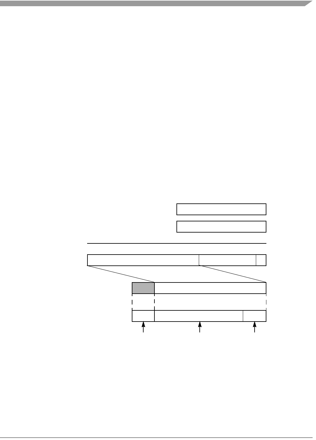
Introduction
MCF548x Reference Manual, Rev. 3
Freescale Semiconductor 4-3
execution times are minimized and deterministic compared to the 2-bit/cycle algorithm with early
termination that the OEP normally uses if no MAC hardware is present.
The added MAC instructions to the ColdFire ISA provide for the multiplication of two numbers, followed
by the addition or subtraction of the product to or from the value in an accumulator. Optionally, the product
may be shifted left or right by 1 bit before addition or subtraction. Hardware support for saturation
arithmetic can be enabled to minimize software overhead when dealing with potential overflow conditions.
Multiply-accumulate operations support 16- or 32-bit input operands of the following formats:
• Signed integers
• Unsigned integers
• Signed, fixed-point, fractional numbers
The EMAC is optimized for single-cycle, pipelined 32 ×32 multiplications. For word- and
longword-sized integer input operands, the low-order 40 bits of the product are formed and used with the
destination accumulator. For fractional operands, the entire 64-bit product is calculated and either
truncated or rounded to the most-significant 40-bit result using the round-to-nearest (even) method before
it is combined with the destination accumulator.
For all operations, the resulting 40-bit product is extended to a 48-bit value (using sign-extension for
signed integer and fractional operands, zero-fill for unsigned integer operands) before being combined
with the 48-bit destination accumulator.
Figure 4-4 and Figure 4-5 show relative alignment of input operands, the full 64-bit product, the resulting
40-bit product used for accumulation, and 48-bit accumulator formats.
Figure 4-4. Fractional Alignment
X
OperandY
OperandX
Product
Extended Product
Accumulator
32
8
Extension Byte Upper [7:0]
+
“0”
32
40 23
40
840 8
Accumulator [31:0] Extension Byte Lower [7:0]
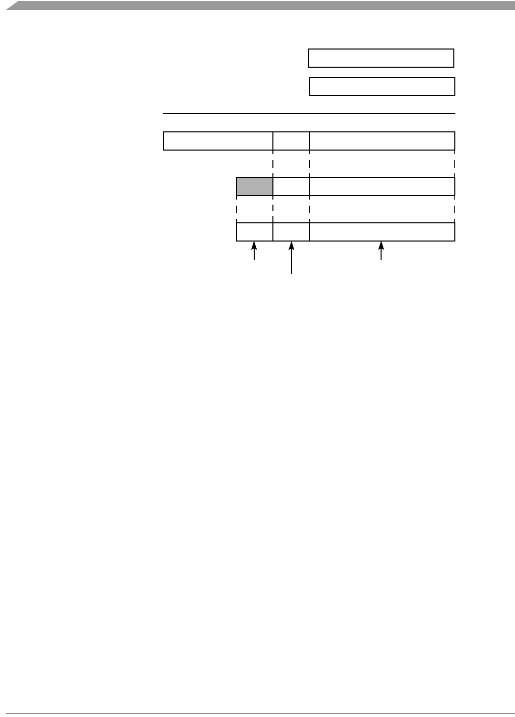
MCF548x Reference Manual, Rev. 3
4-4 Freescale Semiconductor
Figure 4-5. Signed and Unsigned Integer Alignment
Thus, the 48-bit accumulator definition is a function of the EMAC operating mode. Given that each 48-bit
accumulator is the concatenation of 16-bit accumulator extension register (ACCextn) contents and 32-bit
ACCn contents, the specific definitions are as follows:
if MACSR[6:5] == 00/* signed integer mode */
Complete Accumulator[47:0] = {ACCextn[15:0], ACCn[31:0]}
if MACSR[6:5] == -1/* signed fractional mode */
Complete Accumulator [47:0] = {ACCextn[15:8], ACCn[31:0], ACCextn[7:0]}
if MACSR[6:5] == 10/* unsigned integer mode */
Complete Accumulator[47:0] = {ACCextn[15:0], ACCn[31:0]}
The four accumulators are represented as an array, ACCn, where n selects the register.
Although the multiplier array is implemented in a four-stage pipeline, all arithmetic MAC instructions
have an effective issue rate of 1 cycle, regardless of input operand size or type.
All arithmetic operations use register-based input operands, and summed values are stored internally in an
accumulator. Thus, an additional move instruction is needed to store data in a general-purpose register.
One new feature found in EMAC instructions is the ability to choose the upper or lower word of a register
as a 16-bit input operand. This is useful in filtering operations if one data register is loaded with the input
data and another is loaded with the coefficient. Two 16-bit multiply accumulates can be performed without
fetching additional operands between instructions by alternating the word choice during the calculations.
The EMAC has four accumulator registers versus the MAC’s one accumulator. The additional registers
improve the performance of some algorithms by minimizing pipeline stalls needed to store an accumulator
value back to general-purpose registers. Many algorithms require multiple calculations on a given data set.
By applying different accumulators to these calculations, it is often possible to store one accumulator
without any stalls while performing operations involving a different destination accumulator.
X
OperandY
OperandX
Product
Extended Product
Accumulator
32
32
32
32
32
8
8
8
24
8
8
+
Extension Byte Upper [7:0]
Extension Byte Lower [7:0]
Accumulator [31:0]

Memory Map/Register Definition
MCF548x Reference Manual, Rev. 3
Freescale Semiconductor 4-5
The need to move large amounts of data presents an obstacle to obtaining high throughput rates in DSP
engines. New and existing ColdFire instructions can accommodate these requirements. A MOVEM
instruction can move large blocks of data efficiently by generating line-sized burst transfers. The ability to
simultaneously load an operand from memory into a register and execute a MAC instruction makes some
DSP operations such as filtering and convolution more manageable.
The programming model includes a 16-bit mask register (MASK), which can optionally be used to
generate an operand address during MAC + MOVE instructions. The application of this register with
auto-increment addressing mode supports efficient implementation of circular data queues for memory
operands.
The additional MAC status register (MACSR) contains a 4-bit operational mode field and condition flags.
Operational mode bits control whether operands are signed or unsigned and whether they are treated as
integers or fractions. These bits also control the overflow/saturation mode and the way in which rounding
is performed. Negative, zero, and multiple overflow condition flags are also provided.
4.2 Memory Map/Register Definition
The EMAC provides the following program-visible registers:
• Four 32-bit accumulators (ACCn = ACC0, ACC1, ACC2, and ACC3)
• Eight 8-bit accumulator extensions (two per accumulator), packaged as two 32-bit values for load
and store operations (ACCext01 and ACCext23)
• One 16-bit mask register (MASK)
• One 32-bit MAC status register (MACSR) including four indicator bits signaling product or
accumulation overflow (one for each accumulator: PAV0–PAV3)
These registers are shown in Figure 4-6.
Figure 4-6. EMAC Register Set
4.2.1 MAC Status Register (MACSR)
MACSR functionality is organized as follows:
• MACSR[11–8] contains one product/accumulation overflow flag per accumulator.
• MACSR[7–4] defines the operating configuration of the MAC unit.
• MACSR[3–0] contains indicator flags from the last MAC instruction execution.
31 0
MACSR MAC status register
ACC0 MAC accumulator 0
ACC1 MAC accumulator 1
ACC2 MAC accumulator 2
ACC3 MAC accumulator 3
ACCext01 Extensions for ACC0 and ACC1
ACCext23 Extensions for ACC2 and ACC3
MASK MAC mask register

MCF548x Reference Manual, Rev. 3
4-6 Freescale Semiconductor
Table 4-1 describes MACSR fields.
31 30 29 28 27 26 25 24 23 22 21 20 19 18 17 16
R0000000000000000
W
Reset0000000000000000
15 14 13 12 11 10 9 8 7 6 5 4 3 2 1 0
R 0 0 0 0 PAVx OMC S/U F/I R/T N Z V EV
W
Reset0000000000000000
Reg
Addr
Figure 4-7. MAC Status Register (MACSR)
Table 4-1. MACSR Field Descriptions
Bits Name Description
31–12 — Reserved, should be cleared.
11–8 PAVxProduct/accumulation overflow flags. Contains four flags, one per accumulator, that indicate if past
MAC or MSAC instructions generated an overflow during product calculation or the 48-bit
accumulation. When a MAC or MSAC instruction is executed, the PAVx flag associated with the
destination accumulator is used to form the general overflow flag, MACSR[V]. Once set, each flag
remains set until V is cleared by a MOV.L , MACSR instruction or the accumulator is loaded directly.
7 OMC Operational mode field: Overflow/saturation mode. Used to enable or disable saturation mode on
overflow. If set, the accumulator is set to the appropriate constant on any operation which overflows
the accumulator. Once saturated, the accumulator remains unaffected by any other MAC or MSAC
instructions until either the overflow bit is cleared or the accumulator is directly loaded.
6 S/U Operational mode field: Signed/unsigned operations.
In integer mode:
S/U determines whether operations performed are signed or unsigned. It also determines the
accumulator value during saturation, if enabled.
0 Signed numbers. On overflow, if OMC is enabled, an accumulator saturates to the most positive
(0x7FFF_FFFF) or the most negative (0x8000_0000) number, depending on both the instruction
and the value of the product that overflowed.
1 Unsigned numbers. On overflow, if OMC is enabled, an accumulator saturates to the smallest
value (0x0000_0000) or the largest value (0xFFFF_FFFF), depending on the instruction.
In fractional mode:
S/U controls rounding while storing an accumulator to a general-purpose register.
0 Move accumulator without rounding to a 16-bit value. Accumulator is moved to a general-purpose
register as a 32-bit value.
1 The accumulator is rounded to a 16-bit value using the round-to-nearest (even) method when it
is moved to a general-purpose register. See Section 4.2.1.1.1, “Rounding.” The resulting 16-bit
value is stored in the lower word of the destination register. The upper word is zero-filled. The
accumulator value is not affected by this rounding procedure.

Memory Map/Register Definition
MCF548x Reference Manual, Rev. 3
Freescale Semiconductor 4-7
Table 4-2 summarizes the interaction of the MACSR[S/U,F/I,R/T] control bits.
5 F/I Operational mode field: Fractional/integer mode Determines whether input operands are treated as
fractions or integers.
0 Integers can be represented in either signed or unsigned notation, depending on the value of S/U.
1 Fractions are represented in signed, fixed-point, two’s complement notation. Values range from
-1 to 1- 2-15 for 16-bit fractions and -1 to 1 - 2-31 for 32-bit fractions. See Section 4.3.2, “Data
Representation."
4 R/T Operational mode field: Round/truncate mode. Controls the rounding procedure for MOV.L
ACCx,Rx, or MSAC.L instructions when operating in fractional mode.
0 Truncate. The product’s lsbs are dropped before it is combined with the accumulator. Additionally,
when a store accumulator instruction is executed (MOV.L ACCx,Rx), the 8 lsbs of the 48-bit
accumulator logic are simply truncated.
1 Round-to-nearest (even). The 64-bit product of two 32-bit, fractional operands is rounded to the
nearest 40-bit value. If the low-order 24 bits equal 0x80_0000, the upper 40 bits are rounded to
the nearest even (lsb = 0) value.See Section 4.2.1.1.1, “Rounding.” Additionally, when a store
accumulator instruction is executed (MOV.L ACCx,Rx), the lsbs of the 48-bit accumulator logic are
used to round the resulting 16- or 32-bit value. If MACSR[S/U] = 0 and MACSR[R/T] = 1, the
low-order 8 bits are used to round the resulting 32-bit fraction. If MACSR[S/U] = 1, the low-order
24 bits are used to round the resulting 16-bit fraction.
3 N Negative flag. Set if the msb of the result is set, otherwise cleared. N is affected only by MAC, MSAC,
and load operations; it is not affected by MULS and MULU instructions.
2 Z Zero flag. Set if the result equals zero, otherwise cleared. This bit is affected only by MAC, MSAC,
and load operations; it is not affected by MULS and MULU instructions.
1 V Overflow flag. Set if an arithmetic overflow occurs on a MAC or MSAC instruction indicating that the
result cannot be represented in the limited width of the EMAC. V is set only if a product overflow
occurs or the accumulation overflows the 48-bit structure. V is evaluated on each MAC or MSAC
operation and uses the appropriate PAVx flag in the next-state V evaluation.
0 EV Extension overflow flag. Signals that the last MAC or MSAC instruction overflowed the 32 lsbs in
integer mode or the 40 lsbs in fractional mode of the destination accumulator. However, the result is
still accurately represented in the combined 48-bit accumulator structure. Although an overflow has
occurred, the correct result, sign, and magnitude are contained in the 48-bit accumulator.
Subsequent MAC or MSAC operations may return the accumulator to a valid 32/40-bit result.
Table 4-1. MACSR Field Descriptions (Continued)
Bits Name Description

MCF548x Reference Manual, Rev. 3
4-8 Freescale Semiconductor
4.2.1.1 Fractional Operation Mode
This section describes behavior when the fractional mode is used (MACSR[F/I] is set).
4.2.1.1.1 Rounding
When the processor is in fractional mode, there are two operations during which rounding can occur.
• Execution of a store accumulator instruction (MOV.L ACCx,Rx). The lsbs of the 48-bit
accumulator logic are used to round the resulting 16- or 32-bit value. If MACSR[S/U] is cleared,
the low-order 8 bits are used to round the resulting 32-bit fraction. If MACSR[S/U] is set, the
low-order 24 bits are used to round the resulting 16-bit fraction.
• Execution of a MAC (or MSAC) instruction with 32-bit operands. If MACSR[R/T] is zero,
multiplying two 32-bit numbers creates a 64-bit product that is truncated to the upper 40 bits;
otherwise, it is rounded using round-to-nearest (even) method.
To understand the round-to-nearest-even method, consider the following example involving the rounding
of a 32-bit number, R0, to a 16-bit number. Using this method, the 32-bit number is rounded to the closest
16-bit number possible. Let the high-order 16 bits of R0 be named R0.U and the low-order 16 bits be R0.L.
• If R0.L is less than 0x8000, the result is truncated to the value of R0.U.
• If R0.L is greater than 0x8000, the upper word is incremented (rounded up).
• If R0.L is 0x8000, R0 is half-way between two 16-bit numbers. In this case, rounding is based on
the lsb of R0.U, so the result is always even (lsb = 0).
— If the lsb of R0.U = 1 and R0.L = 0x8000, the number is rounded up.
— If the lsb of R0.U = 0 and R0.L =0x8000, the number is rounded down.
This method minimizes rounding bias and creates as statistically correct an answer as possible.
The rounding algorithm is summarized in the following pseudocode:
if R0.L < 0x8000
then Result = R0.U
else if R0.L > 0x8000
Table 4-2. Summary of S/U, F/I, and R/T Control Bits
S/U F/I R/T Operational Modes
0 0 x Signed, integer
0 1 0 Signed, fractional
Truncate on MAC.L and MSAC.L
No round on accumulator stores
0 1 1 Signed, fractional
Round on MAC.L and MSAC.L
Round-to-32-bits on accumulator stores
1 0 x Unsigned, integer
1 1 0 Signed, fractional
Truncate on MAC.L and MSAC.L
Round-to-16-bits on accumulator stores
1 1 1 Signed, fractional
Round on MAC.L and MSAC.L
Round-to-16-bits on accumulator stores

Memory Map/Register Definition
MCF548x Reference Manual, Rev. 3
Freescale Semiconductor 4-9
then Result = R0.U + 1
else if lsb of R0.U = 0 /* R0.L = 0x8000 */
then Result = R0.U
else Result = R0.U + 1
The round-to-nearest-even technique is also known as convergent rounding.
4.2.1.1.2 Saving and Restoring the EMAC Programming Model
The presence of rounding logic in the output datapath of the EMAC requires that special care be taken
during the EMAC’s save/restore process. In particular, any result rounding modes must be disabled during
the save/restore process so the exact bit-wise contents of the EMAC registers are accessed. Consider the
following memory structure containing the EMAC programming model:
struct macState {
int acc0;
int acc1;
int acc2;
int acc3;
int accext01;
int accext02;
int mask;
int macsr;
} macState;
The following assembly language routine shows the proper sequence for a correct EMAC state save. This
code assumes all Dn and An registers are available for use and the memory location of the state save is
defined by A7.
EMAC_state_save:
move.l macsr,d7 ; save the macsr
clr.l d0 ; zero the register to ...
move.l d0,macsr ; disable rounding in the macsr
move.l acc0,d0 ; save the accumulators
move.l acc1,d1
move.l acc2,d2
move.l acc3,d3
move.l accext01,d4 ; save the accumulator extensions
move.l accext23,d5
move.l mask,d6 ; save the address mask
movem.l #0x00ff,(a7) ; move the state to memory
The following code performs the EMAC state restore:
EMAC_state_restore:
movem.l (a7),#0x00ff ; restore the state from memory
move.l #0,macsr ; disable rounding in the macsr
move.l d0,acc0 ; restore the accumulators
move.l d1,acc1
move.l d2,acc2
move.l d3,acc3
move.l d4,accext01 ; restore the accumulator extensions
move.l d5,accext23

MCF548x Reference Manual, Rev. 3
4-10 Freescale Semiconductor
move.l d6,mask ; restore the address mask
move.l d7,macsr ; restore the macsr
By executing this type of sequence, the exact state of the EMAC programming model can be correctly
saved and restored.
4.2.1.1.3 MULS/MULU
MULS and MULU are unaffected by fractional mode operation; operands are still assumed to be integers.
4.2.1.1.4 Scale Factor in MAC or MSAC Instructions
The scale factor is ignored while the MAC is in fractional mode.
4.2.2 Mask Register (MASK)
The 32-bit MASK implements the low-order 16 bits to minimize the alignment complications involved
with loading and storing only 16 bits. When the MASK is loaded, the low-order 16 bits of the source
operand are actually loaded into the register. When it is stored, the upper 16 bits are all forced to ones.
This register performs a simple AND with the operand address for MAC instructions. That is, the
processor calculates the normal operand address and, if enabled, that address is then ANDed with
{0xFFFF, MASK[15:0]} to form the final address. Therefore, with certain MASK bits cleared, the operand
address can be constrained to a certain memory region. This is used primarily to implement circular queues
in conjunction with the (An)+ addressing mode.
This feature minimizes the addressing support required for filtering, convolution, or any routine that
implements a data array as a circular queue. For MAC + MOVE operations, the MASK contents can
optionally be included in all memory effective address calculations. The syntax is as follows:
MAC.sz Ry,RxSF,<ea>y&,Rw
The & operator enables the use of MASK and causes bit 5 of the extension word to be set. The exact
algorithm for the use of MASK is as follows:
if extension word, bit [5] = 1, the MASK bit, then
if <ea> = (An)
oa = An & {0xFFFF, MASK}
if <ea> = (An)+
oa = An
An = (An + 4) & {0xFFFF, MASK}
if <ea> =-(An)
oa = (An - 4) & {0xFFFF, MASK}
An = (An - 4) & {0xFFFF, MASK}
if <ea> = (d16,An)
oa = (An + se_d16) & {0xFFFF0x, MASK}
Here, oa is the calculated operand address and se_d16 is a sign-extended 16-bit displacement. For
auto-addressing modes of post-increment and pre-decrement, the calculation of the updated An value is
also shown.
Use of the post-increment addressing mode, {(An)+} with the MASK is suggested for circular queue
implementations.

EMAC Instruction Set Summary
MCF548x Reference Manual, Rev. 3
Freescale Semiconductor 4-11
4.3 EMAC Instruction Set Summary
Table 4-3 summarizes EMAC unit instructions.
4.3.1 EMAC Instruction Execution Timing
The instruction execution times for the EMAC can be found in Section 3.7, “Instruction Execution
Timing.”
The ColdFire family supports two multiply-accumulate implementations that provide different levels of
performance and capability for differing silicon costs. The EMAC features a four-stage execution pipeline,
optimized for 32-bit operands with a fully-pipelined 32 × 32 multiply array and four 48-bit accumulators.
The EMAC execution pipeline overlaps the AGEX stage of the OEP; that is, the first stage of the EMAC
pipeline is the last stage of the basic OEP. EMAC units are designed for sustained, fully-pipelined
operation on accumulator load, copy, and multiply-accumulate instructions. However, instructions that
store contents of the multiply-accumulate programming model can generate OEP stalls that expose the
EMAC execution pipeline depth, as in the following:
mac.w Ry, Rx, Acc0
move.l Acc0, Rz
Table 4-3. EMAC Instruction Summary
Command Mnemonic Description
Multiply Signed MULS <ea>y,Dx Multiplies two signed operands yielding a signed result
Multiply Unsigned MULU <ea>y,Dx Multiplies two unsigned operands yielding an unsigned result
Multiply Accumulate MAC Ry,RxSF,ACCx
MSAC Ry,RxSF,ACCx
Multiplies two operands and adds/subtracts the product to/from an
accumulator
Multiply Accumulate
with Load
MAC Ry,Rx,<ea>y,Rw,ACCx
MSAC Ry,Rx,<ea>y,Rw,ACCx
Multiplies two operands and combines the product to an
accumulator while loading a register with the memory operand
Load Accumulator MOV.L {Ry,#imm},ACCx Loads an accumulator with a 32-bit operand
Store Accumulator MOV.L ACCx,Rx Writes the contents of an accumulator to a CPU register
Copy Accumulator MOV.L ACCy,ACCx Copies a 48-bit accumulator
Load MACSR MOV.L {Ry,#imm},MACSR Writes a value to MACSR
Store MACSR MOV.L MACSR,Rx Write the contents of MACSR to a CPU register
Store MACSR to CCR MOV.L MACSR,CCR Write the contents of MACSR to the CCR
Load MAC Mask Reg MOV.L {Ry,#imm},MASK Writes a value to the MASK register
Store MAC Mask Reg MOV.L MASK,Rx Writes the contents of the MASK to a CPU register
Load AccExtensions01 MOV.L {Ry,#imm},ACCext01 Loads the accumulator 0,1 extension bytes with a 32-bit operand
Load AccExtensions23 MOV.L {Ry,#imm},ACCext23 Loads the accumulator 2,3 extension bytes with a 32-bit operand
Store AccExtensions01 MOV.L ACCext01,Rx Writes the contents of accumulator 0,1 extension bytes into a CPU
register
Store AccExtensions23 MOV.L ACCext23,Rx Writes the contents of accumulator 2,3 extension bytes into a CPU
register
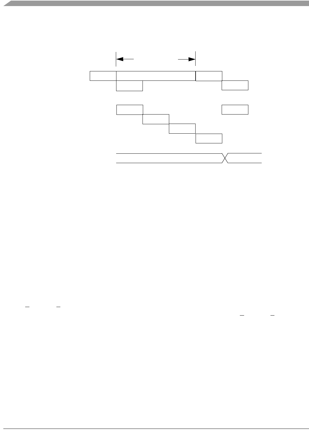
MCF548x Reference Manual, Rev. 3
4-12 Freescale Semiconductor
The mov.l instruction that stores the accumulator to an integer register (Rz) stalls until the program-visible
copy of the accumulator is available. Figure 4-8 shows EMAC timing.
Figure 4-8. EMAC-Specific OEP Sequence Stall
In Figure 4-8, the OEP stalls the store-accumulator instruction for 3 cycles: the depth of the EMAC
pipeline minus 1. The minus 1 factor is needed because the OEP and EMAC pipelines overlap by a cycle,
the AGEX stage. As the store-accumulator instruction reaches the AGEX stage where the operation is
performed, the just-updated accumulator 0 value is available.
As with change or use stalls between accumulators and general-purpose registers, introducing intervening
instructions that do not reference the busy register can reduce or eliminate sequence-related store-MAC
instruction stalls. In fact, a major benefit of the EMAC is the addition of three accumulators to minimize
stalls caused by exchanges between the accumulator(s) and the general-purpose registers.
4.3.2 Data Representation
MACSR[S/U,F/I] selects one of the following three modes, where each mode defines a unique operand
type:
• Two’s complement signed integer: In this format, an N-bit operand value lies in the range -2(N-1)
< operand < 2(N-1) - 1. The binary point is right of the lsb.
• Unsigned integer: In this format, an N-bit operand value lies in the range 0 < operand < 2N - 1. The
binary point is right of the lsb.
• Two’s complement, signed fractional: In an N-bit number, the first bit is the sign bit. The remaining
bits signify the first N-1 bits after the binary point. Given an N-bit number, aN-1aN-2aN-3... a2a1a0,
its value is given by the equation in Figure 4-9.
Figure 4-9. Two’s Complement, Signed Fractional Equation
DSOC
AGEX
mac
mac
EMAC EX1
EMAC EX2
EMAC EX3
EMAC EX4
mac
mac
mac
mac
mov
mov
mov
mov
Three-cycle
regBusy stall
Accumulator 0 old new
value 1 aN1–
⋅()–2
i1N–+()
ai⋅
i0=
N2–
∑
+=

EMAC Instruction Set Summary
MCF548x Reference Manual, Rev. 3
Freescale Semiconductor 4-13
This format can represent numbers in the range -1 < operand < 1 - 2(N-1).
For words and longwords, the largest negative number that can be represented is -1, whose internal
representation is 0x8000 and 0x8000_0000, respectively. The largest positive word is 0x7FFF or (1 - 2-15);
the most positive longword is 0x7FFF_FFFF or (1 - 2-31).
4.3.3 EMAC Opcodes
EMAC opcodes are described in the ColdFire Programmer’s Reference Manual. Note the following:
• Unless otherwise noted, the value of MACSR[N,Z] is based on the result of the final operation that
involves the product and the accumulator.
• The overflow (V) flag is handled differently. It is set if the complete product cannot be represented
as a 40-bit value (this applies to 32 ×32 integer operations only) or if the combination of the
product with an accumulator cannot be represented in the given number of bits. The EMAC design
includes an additional product/accumulation overflow bit for each accumulator that are treated as
sticky indicators and are used to calculate the V bit on each MAC or MSAC instruction. See
Section 4.2.1, “MAC Status Register (MACSR).”
• For the MAC design, the assembler syntax of the MAC (multiply and add to accumulator) and
MSAC (multiply and subtract from accumulator) instructions does not include a reference to the
single accumulator. For the EMAC, it is expected that assemblers support this syntax and that no
explicit reference to an accumulator is interpreted as a reference to ACC0. These assemblers would
also support syntaxes where the destination accumulator is explicitly defined.
• The optional 1-bit shift of the product is specified using the notation {<< | >>} SF, where <<1
indicates a left shift and >>1 indicates a right shift. The shift is performed before the product is
added to or subtracted from the accumulator. Without this operator, the product is not shifted. If the
EMAC is in fractional mode (MACSR[F/I] is set), SF is ignored and no shift is performed. Because
a product can overflow, the following guidelines are implemented:
— For unsigned word and longword operations, a zero is shifted into the product on right shifts.
— For signed, word operations, the sign bit is shifted into the product on right shifts unless the
product is zero. For signed, longword operations, the sign bit is shifted into the product unless
an overflow occurs or the product is zero, in which case a zero is shifted in.
— For all left shifts, a zero is inserted into the lsb position.
The following pseudocode explains basic MAC or MSAC instruction functionality. This example is
presented as a case statement covering the three basic operating modes with signed integers, unsigned
integers, and signed fractionals. Throughout this example, a comma-separated list in curly brackets, {},
indicates a concatenation operation.
switch (MACSR[6:5]) /* MACSR[S/U, F/I] */
{
case 0: /* signed integers */
if (MACSR.OMC == 0 || MACSR.PAVx == 0)
then {
MACSR.PAVx = 0
/* select the input operands */
if (sz == word)
then {if (U/Ly == 1)
then operandY[31:0] = {sign-extended Ry[31], Ry[31:16]}
else operandY[31:0] = {sign-extended Ry[15], Ry[15:0]}
if (U/Lx == 1)
then operandX[31:0] = {sign-extended Rx[31], Rx[31:16]}
else operandX[31:0] = {sign-extended Rx[15], Rx[15:0]}

MCF548x Reference Manual, Rev. 3
4-14 Freescale Semiconductor
}
else {operandY[31:0] = Ry[31:0]
operandX[31:0] = Rx[31:0]
}
/* perform the multiply */
product[63:0] = operandY[31:0] * operandX[31:0]
/* check for product overflow */
if ((product[63:39] != 0x0000_00_0) && (product[63:39] != 0xfff
f_ff_1))
then { /* product overflow */
MACSR.PAVx = 1
MACSR.V = 1
if (inst == MSAC && MACSR.OMC == 1)
then if (product[63] == 1)
then result[47:0] = 0x0000_7fff_ffff
else result[47:0] = 0xffff_8000_0000
else if (MACSR.OMC == 1)
then /* overflowed MAC,
saturationMode enabled */
if (product[63] == 1)
then result[47:0] = 0xffff_8000_0000
else result[47:0] = 0x0000_7fff_ffff
}
/* sign-extend to 48 bits before performing any scaling */
product[47:40] = {8{product[39]}} /* sign-extend */
/* scale product before combining with accumulator */
switch (SF) /* 2-bit scale factor */
{
case 0: /* no scaling specified */
break;
case 1: /* SF = “<< 1” */
product[40:0] = {product[39:0], 0}
break;
case 2: /* reserved encoding */
break;
case 3: /* SF = “>> 1” */
product[39:0] = {product[39], product[39:1]}
break;
}
if (MACSR.PAVx == 0)
then {if (inst == MSAC)
then result[47:0] = ACCx[47:0] - product[47:0]
else result[47:0] = ACCx[47:0] + product[47:0]
}
/* check for accumulation overflow */
if (accumulationOverflow == 1)
then {MACSR.PAVx = 1

EMAC Instruction Set Summary
MCF548x Reference Manual, Rev. 3
Freescale Semiconductor 4-15
MACSR.V = 1
if (MACSR.OMC == 1)
then /* accumulation overflow,
saturationMode enabled */
if (result[47] == 1)
then result[47:0] = 0x0000_7fff_ffff
else result[47:0] = 0xffff_8000_0000
}
/* transfer the result to the accumulator */
ACCx[47:0] = result[47:0]
}
MACSR.V = MACSR.PAVx
MACSR.N = ACCx[47]
if (ACCx[47:0] == 0x0000_0000_0000)
then MACSR.Z = 1
else MACSR.Z = 0
if ((ACCx[47:31] == 0x0000_0) || (ACCx[47:31] == 0xffff_1))
then MACSR.EV = 0
else MACSR.EV = 1
break;
case 1,3: /* signed fractionals */
if (MACSR.OMC == 0 || MACSR.PAVx == 0)
then {
MACSR.PAVx = 0
if (sz == word)
then {if (U/Ly == 1)
then operandY[31:0] = {Ry[31:16], 0x0000}
else operandY[31:0] = {Ry[15:0], 0x0000}
if (U/Lx == 1)
then operandX[31:0] = {Rx[31:16], 0x0000}
else operandX[31:0] = {Rx[15:0], 0x0000}
}
else {operandY[31:0] = Ry[31:0]
operandX[31:0] = Rx[31:0]
}
/* perform the multiply */
product[63:0] = (operandY[31:0] * operandX[31:0]) << 1
/* check for product rounding */
if (MACSR.R/T == 1)
then { /* perform convergent rounding */
if (product[23:0] > 0x80_0000)
then product[63:24] = product[63:24] + 1
else if ((product[23:0] == 0x80_0000) && (product[24] == 1))
then product[63:24] = product[63:24] + 1
}
/* sign-extend to 48 bits and combine with accumulator */
/* check for the -1 * -1 overflow case */
if ((operandY[31:0] == 0x8000_0000) && (operandX[31:0] == 0x8000_0000))
then product[71:64] = 0x00 /* zero-fill */
else product[71:64] = {8{product[63]}} /* sign-extend */
if (inst == MSAC)
then result[47:0] = ACCx[47:0] - product[71:24]
else result[47:0] = ACCx[47:0] + product[71:24]

MCF548x Reference Manual, Rev. 3
4-16 Freescale Semiconductor
/* check for accumulation overflow */
if (accumulationOverflow == 1)
then {MACSR.PAVx = 1
MACSR.V = 1
if (MACSR.OMC == 1)
then /* accumulation overflow,
saturationMode enabled */
if (result[47] == 1)
then result[47:0] = 0x007f_ffff_ff00
else result[47:0] = 0xff80_0000_0000
}
/* transfer the result to the accumulator */
ACCx[47:0] = result[47:0]
}
MACSR.V = MACSR.PAVx
MACSR.N = ACCx[47]
if (ACCx[47:0] == 0x0000_0000_0000)
then MACSR.Z = 1
else MACSR.Z = 0
if ((ACCx[47:39] == 0x00_0) || (ACCx[47:39] == 0xff_1))
then MACSR.EV = 0
else MACSR.EV = 1
break;
case 2: /* unsigned integers */
if (MACSR.OMC == 0 || MACSR.PAVx == 0)
then {
MACSR.PAVx = 0
/* select the input operands */
if (sz == word)
then {if (U/Ly == 1)
then operandY[31:0] = {0x0000, Ry[31:16]}
else operandY[31:0] = {0x0000, Ry[15:0]}
if (U/Lx == 1)
then operandX[31:0] = {0x0000, Rx[31:16]}
else operandX[31:0] = {0x0000, Rx[15:0]}
}
else {operandY[31:0] = Ry[31:0]
operandX[31:0] = Rx[31:0]
}
/* perform the multiply */
product[63:0] = operandY[31:0] * operandX[31:0]
/* check for product overflow */
if (product[63:40] != 0x0000_00)
then { /* product overflow */
MACSR.PAVx = 1
MACSR.V = 1
if (inst == MSAC && MACSR.OMC == 1)
then result[47:0] = 0x0000_0000_0000
else if (MACSR.OMC == 1)
then /* overflowed MAC,
saturationMode enabled */

EMAC Instruction Set Summary
MCF548x Reference Manual, Rev. 3
Freescale Semiconductor 4-17
result[47:0] = 0xffff_ffff_ffff
}
/* zero-fill to 48 bits before performing any scaling */
product[47:40] = 0 /* zero-fill upper byte */
/* scale product before combining with accumulator */
switch (SF) /* 2-bit scale factor */
{
case 0: /* no scaling specified */
break;
case 1: /* SF = “<< 1” */
product[40:0] = {product[39:0], 0}
break;
case 2: /* reserved encoding */
break;
case 3: /* SF = “>> 1” */
product[39:0] = {0, product[39:1]}
break;
}
/* combine with accumulator */
if (MACSR.PAVx == 0)
then {if (inst == MSAC)
then result[47:0] = ACCx[47:0] - product[47:0]
else result[47:0] = ACCx[47:0] + product[47:0]
}
/* check for accumulation overflow */
if (accumulationOverflow == 1)
then {MACSR.PAVx = 1
MACSR.V = 1
if (inst == MSAC && MACSR.OMC == 1)
then result[47:0] = 0x0000_0000_0000
else if (MACSR.OMC == 1)
then /* overflowed MAC,
saturationMode enabled */
result[47:0] = 0xffff_ffff_ffff
}
/* transfer the result to the accumulator */
ACCx[47:0] = result[47:0]
}
MACSR.V = MACSR.PAVx
MACSR.N = ACCx[47]
if (ACCx[47:0] == 0x0000_0000_0000)
then MACSR.Z = 1
else MACSR.Z = 0
if (ACCx[47:32] == 0x0000)
then MACSR.EV = 0
else MACSR.EV = 1
break;
}

MCF548x Reference Manual, Rev. 3
4-18 Freescale Semiconductor

MCF548x Reference Manual, Rev. 3
Freescale Semiconductor 5-1
Chapter 5
Memory Management Unit (MMU)
This chapter describes the ColdFire virtual memory management unit (MMU), which provides
virtual-to-physical address translation and memory access control. The MMU consists of memory-mapped
control, status, and fault registers that provide access to translation-lookaside buffers (TLBs). Software can
control address translation and access attributes of a virtual address by configuring MMU control registers
and loading TLBs. With software support, the MMU provides demand-paged, virtual addressing.
5.1 Features
The MMU has the following features:
• MMU memory-mapped control, status, and fault registers
— Support a flexible, software-defined virtual environment
— Provide control and maintenance of TLBs
— Provide fault status and recovery information functions
• Separate, 32-entry, fully associative instruction and data TLBs (Harvard TLBs)
— Resides in the controller
— Operates in parallel with the memories
— Suffers no performance penalty on TLB hits
— Supports 1-, 4-, and 8-Kbyte and 1-Mbyte page sizes concurrently
— Contains register-based TLB entries
• Core extensions:
— User stack pointer
— All access error exceptions are precise and recoverable
• Harvard TLB provides 97% of baseline performance on large embedded applications using
equivalent V4 without MMU support as a baseline.
5.2 Virtual Memory Management Architecture
The ColdFire memory management architecture provides a demand-paged, virtual-address environment
with hardware address translation acceleration. It supports supervisor/user, read, write, and execute
permission checking on a per-memory request basis.
The architecture defines the MMU TLB, associated control logic, TLB hit/miss logic, address translation
based on the TLB contents, and access faults due to TLB misses and access violations. It intentionally
leaves some virtual environment details undefined to maximize the software-defined flexibility. These
include the exact structure of the memory-resident pointer descriptor/page descriptor tables, the base
registers for these tables, the exact information stored in the tables, the methodology (if any) for
maintenance of access, and written information on a per-page basis.
5.2.1 MMU Architecture Features
To add optional virtual addressing support, demand-page support, permission checking, and hardware
address translation acceleration to the ColdFire architecture, the MMU architecture features the following:
• Addresses from the core to the MMU are treated as physical or virtual addresses.

MCF548x Reference Manual, Rev. 3
5-2 Freescale Semiconductor
• The address access control logic, address attribute logic, memories, and controller function as in
previous ColdFire versions with the addition of the MMU. The MMU, its TLB, and associated
control reside in the logic.
• The MMU appears as a memory-mapped device in the space. Information for access error fault
processing is stored in the MMU.
• A precise fault (transfer error acknowledge) signals the core on translation (TLB miss) and access
faults. The core supports an instruction restart model for this fault class. Note that this structure
uses the existing ColdFire access error fault vector and needs no new ColdFire exception stack
frames.
• The following additions are made to the memory access control to better support the fault
processing and memory maintenance necessary for this virtual addressing environment. These
additions improve memory performance and functionality for physical and virtual address
environments:
— New supervisor-protect bits to the access control registers (ACRs) and the cache control
register (CACR)
— Improved addressing of the ACRs
5.2.2 MMU Architecture Location
Figure 5-1 shows the placement of the MMU/TLB hardware. It follows a traditional model in which it is
closely coupled to the processor local-memory controllers.
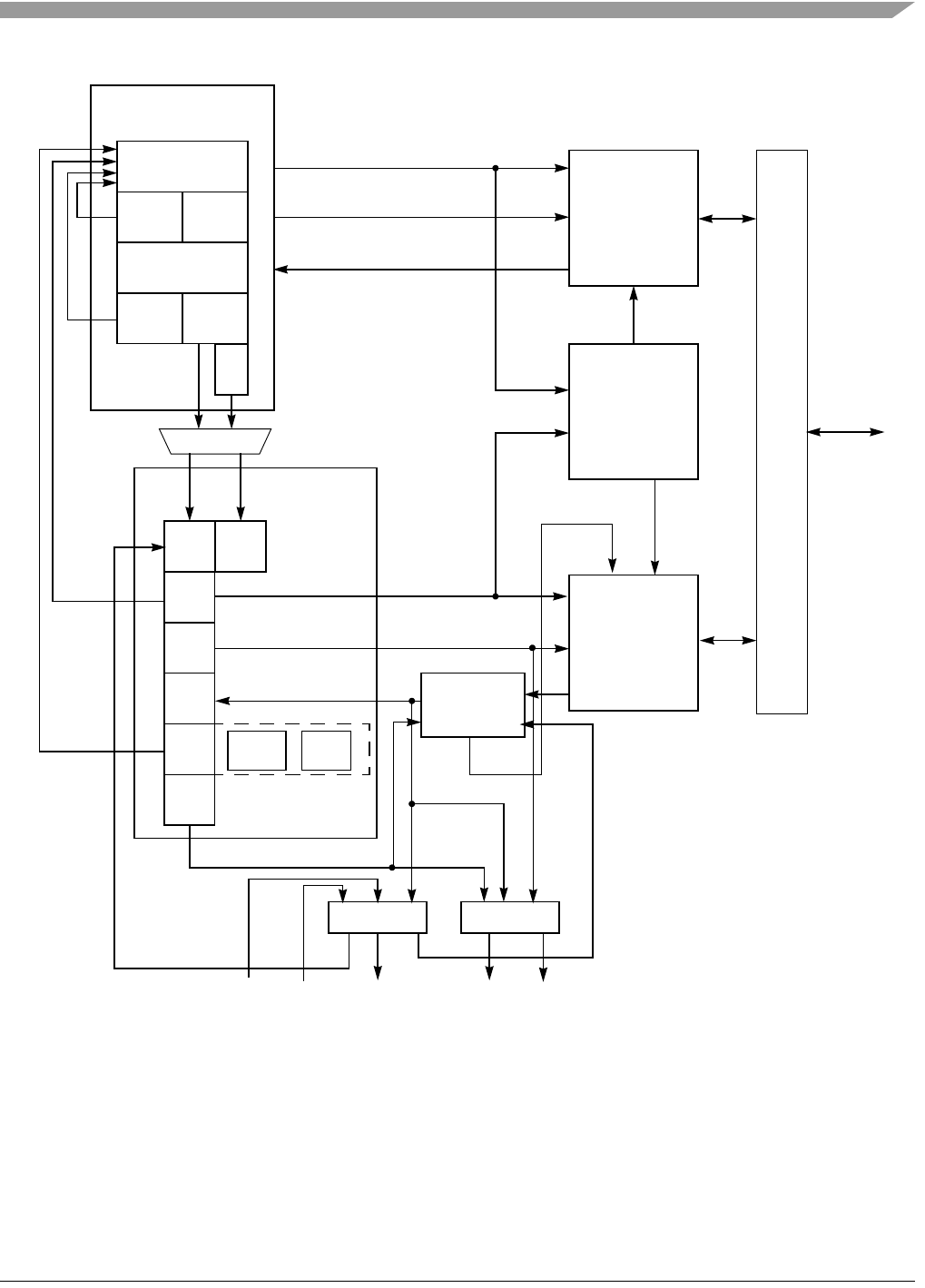
Virtual Memory Management Architecture
MCF548x Reference Manual, Rev. 3
Freescale Semiconductor 5-3
Figure 5-1. CF4e Processor Core Block with MMU
5.2.3 MMU Architecture Implementation
This section describes ColdFire design additions and changes for the MMU architecture. It includes
precise faults, MMU access, virtual mode, virtual memory references, instruction and data cache
addresses, supervisor/user stack pointers, access error stack frame additions, expanded control register
space, ACR address improvements, supervisor protection, and debugging in a virtual environment.
PSTDDATA PSTCLK
Instruction Fetch
IAG
IC1
Branch
Cache
IC2
IED
Branch
Accel.
IB
Operand Execution Pipeline
DS
OAG
OC1
OC2
EX
DA
K2M M Bus
J
KC1
KC2
BDM DDATA
DSCLK DSI DSDO
J
KC1
KC2
Instruction
Memory
Data
Memory
FPU
EMAC
Memory
Management
Physical
KC1
Physical
KC1
Unit
(MMU)
DS
Pipeline
Misalignment
Module

MCF548x Reference Manual, Rev. 3
5-4 Freescale Semiconductor
5.2.3.1 Precise Faults
The MMU architecture performs virtual-to-physical address translation and permission checking in the
core. To support demand-paging, the core design provides a precise, recoverable fault for all references.
5.2.3.2 MMU Access
The MMU TLB control registers are memory-mapped. The TLB entries are read and written indirectly
through the MMU control registers. The memory space for these resources is defined by a new supervisor
program model register, the MMU base address register (MMUBAR). This register defines a
supervisor-mode, data-only space. It has the highest priority for the data address mode determination.
5.2.3.3 Virtual Mode
Every instruction and data reference is either a virtual or physical address mode access. All addresses for
special mode (interrupt acknowledges, emulator mode operations, etc.) accesses are physical. All
addresses are physical if the MMU is not enabled. If the MMU is present and enabled, the address mode
for normal accesses is determined by the MMUBAR, RAMBARs, and ACRs in the priority order listed.
Addresses that hit in the MMUBAR, RAMBARs, and ACRs are treated as physical references. These
addresses are not translated and their address attributes are sourced from the highest priority mapping
register they hit. If an address hits none of these mapping registers, it is a virtual address and is sent to the
MMU. If the MMU is enabled, the default CACR information is not used.
5.2.3.4 Virtual Memory References
The ColdFire MMU architecture references the MMU for all virtual mode accesses to the . MMU, SRAM
and ACR memory spaces are treated as physical address spaces and all permissions that apply to these
spaces are contained in the respective mapping register. The virtual mode access either hits or misses in
the TLB of the MMU. A TLB miss generates an access fault in the processor, allowing software to either
load the appropriate translation into the TLB and restart the faulting instruction or abort the process. Each
TLB hit checks permissions based on the access control information in the referenced TLB entry.
5.2.3.5 Instruction and Data Cache Addresses
For a given page size, virtual address bits that reference within a page are called the in-page address. All
bits above this are the virtual page number. Likewise, the physical address has a physical page number and
in-page address bits. Virtual and physical in-page address bits are the same; the MMU translates the virtual
page number to the physical page number.
Instruction and data caches are accessed with the untranslated address. The translated address is used for
cache allocation. That is, caches are virtual-address accessed and physical-address tagged. If instruction
and data cache addresses are not larger than the in-page address for the smallest active MMU page, the
cache is considered physically accessed; if they are larger, the cache can have aliasing problems between
virtual and cache addresses. Software handles these problems by forcing the virtual address to be equal to
the physical address for those bits addressing the cache, but above the in-page address of the smallest
active page size. The number of these bits depends on cache and page sizes.
Caches are addressed with the virtual address, because the cache uses synchronous memory elements, and
an access starts at the rising-clock edge of the first pipeline stage. The MMU provides a physical address
midway through this cycle.
If the cache set address has fewer bits than the in-page address, the cache is considered physically
addressed because these bits are the same in the virtual and physical addresses. If the cache set address has

Virtual Memory Management Architecture
MCF548x Reference Manual, Rev. 3
Freescale Semiconductor 5-5
more bits than the in-page address, one or more of the low-order virtual page number bits are used to
address the cache. The MMU translates these bits; the resulting low-order physical page number bits are
used to determine cache hits.
Address aliasing problems occur when two virtual addresses access one physical page. This is generally
allowed and, if the page is cacheable, one coherent copy of the page image is mapped in the cache at any
time.
If multiple virtual addresses pointing to the same physical address differ only in the low-order virtual page
number bits, conflicting copies can be allocated. For an 8-Kbyte, 4-way, set-associative cache with a
16-byte line size, the cache set address uses address bits 10–4. If virtual addresses 0x0_1000 and 0x0_1400
are mapped to physical address 0x0_1000, using virtual address 0x0_1000 loads cache set 0x00; using
virtual address 0x0_1400 loads cache set 0x40. This puts two copies of the same physical address in the
cache making this memory space not coherent. To avoid this problem, software must force low-order
virtual page number bits to be equal to low-order physical address bits for all bits used to address the cache
set.
5.2.3.6 Supervisor/User Stack Pointers
To isolate supervisor and user modes, CF4e implements two A7 register stack pointers, one for supervisor
mode (SSP) and one for user mode (USP). Two former M68000 family privileged instructions to load and
store the user stack pointer are restored in the instruction set architecture.
5.2.3.7 Access Error Stack Frame
accesses that fault (that is, terminate with a transfer error acknowledge) generate an access error
exception. MMU TLB misses and access violations use the same fault. To quickly determine if a fault was
due to a TLB miss or another type of access error, new fault status field (FS) encodings in the exception
stack frame signal TLB misses on the following:
• Instruction fetch
• Instruction extension fetch
• Data read
• Data write
See Section 5.4.3, “Access Error Stack Frame Additions,” for more information.
5.2.3.8 Expanded Control Register Space
The MMU base address register (MMUBAR) is added for ColdFire virtual mode. Like other control
registers, it can be accessed from the debug module or written using the privileged MOVEC instruction.
See Section 5.5.3.1, “MMU Base Address Register (MMUBAR).”
5.2.3.9 Changes to ACRs and CACR
New ACR and CACR bits, Table 5-1, improve address granularity and supervisor mode protection. These
improvements are not necessary to implement the ColdFire MMU, but they improve memory
functionality for physical and virtual address environments.

MCF548x Reference Manual, Rev. 3
5-6 Freescale Semiconductor
5.2.3.10 ACR Address Improvements
ACRs provide a 16-Mbyte address window. For a given request address, if the ACR is valid and the request
mode matches the mode specified in the supervisor mode field, ACRn[S], hit determination is specified as
follows:
ACRx_Hit = 0;
if ((address[31:24] & ~ACRn[23:16]) == (ACRn[31:24] & ~ACRn[23:16]))
ACRx_Hit = 1;
With this hit function, ACRs can assign address attributes for user or supervisor requests to memory spaces
of at least 16 Mbytes (through the address mask). With the MMU definition, the ACR hit function is
improved by the address mask mode bit (ACRn[AMM]), which supports finer address granularity. See
Table 5-1.
The revised hit determination becomes the following:
ACRx_Hit = 0;
if (ACRn[10] == 1)
if ((address[31–24] == ACRn[31–24])) &&
((address[23–20] & ~ACRn[19–16]) == (ACRn[23–20] & ~ACRn[19–16])))
ACRx_Hit = 1;
else if (address[31–24] & ~ACRn[23–16]) == (ACRn[31–24] & ~ACRn[23–16]))
ACRx_Hit = 1;
Table 5-1. New ACR and CACR Bits
Bits Name Description
ACRn[10] AMM Address mask mode. Determines access to the associated address space.
0 The ACR hit function is the same as previous versions, allowing control of a 16-Mbyte
or greater memory region.
1 The upper 8 bits of the address and ACR are compared without a mask function; bits
23–20 of the address and ACR are compared masked by ACR[19–16], allowing control
of a 1- to 16-Mbyte region.
Reset value is 0.
ACRn[3] SP Supervisor protect. Determines access to the associated address space.
0 Supervisor and user access allowed.
1 Only supervisor access allowed. Attempted user access causes an access error
exception.
Reset value is 0.
CACR[23] DDSP Default data supervisor protect. Determines access to the associated data space.
0 Supervisor and user access allowed.
1 Only supervisor access allowed. Attempted user access causes an access error
exception.
Reset value is 0.
CACR[7] DISP Default instruction supervisor protect. Determines access to the associated instruction
space.
0 Supervisor and user access allowed.
1 Only supervisor access allowed. Attempted user access causes access error exception
Reset value is 0.

Debugging in a Virtual Environment
MCF548x Reference Manual, Rev. 3
Freescale Semiconductor 5-7
5.2.3.11 Supervisor Protection
Each instruction or data reference is either a supervisor or user access. The CPU’s status register supervisor
bit (SR[S]) determines the operating mode. New ACR and CACR bits protect supervisor space. See
Table 5-1.
5.3 Debugging in a Virtual Environment
To support debugging in a virtual environment, numerous enhancements are implemented in the ColdFire
debug architecture. These enhancements are collectively called Debug revision D and primarily relate to
the addition of an 8-bit address space identifier (ASID) to yield a 40-bit virtual address. This expansion
affects two major debug functions:
• The ASID is optionally included in the hardware breakpoint registers specification. For example,
the four PC breakpoint registers are expanded by 8 bits each, so that a specific ASID value can be
part of the breakpoint instruction address. Likewise, data address/data breakpoint registers are
expanded to include an ASID value. The new control registers define whether and how the ASID
is included in the breakpoint comparison trigger logic.
• The debug module implements the concept of ownership trace in which an ASID value can be
optionally displayed as part of real-time trace. When enabled, real-time trace displays instruction
addresses on any change-of-flow instruction that is not absolute or PC-relative. For Debug revision
D architecture, the address display is expanded to optionally include ASID contents, thus providing
the complete instruction virtual address on these instructions. Additionally, when a Sync_PC serial
BDM command is loaded from the external development system, the processor displays the
complete virtual instruction address, including the 8-bit ASID value.
The MMU control registers are accessible through serial BDM commands. See Chapter 8, “Debug
Support.”
5.4 Virtual Memory Architecture Processor Support
To support the MMU, enhancements have been made to the exception model, the stack pointers, and the
access error stack frame.
5.4.1 Precise Faults
To support demand-paging, all memory references require precise, recoverable faults. The ColdFire
instruction restart mechanism ensures that a faulted instruction restarts from the beginning of execution;
that is, no internal state information is saved when an exception occurs and none is restored when the
handler ends. Given the PC address defined in the exception stack frame, the processor reestablishes
program execution by transferring control to the given location as part of the RTE (return from exception)
instruction.
For a detailed description, see Section 3.9, “Precise Faults.”
5.4.2 Supervisor/User Stack Pointers
To provide the required isolation between these operating modes as dictated by a virtual memory
management scheme, a user stack pointer (A7–USP) is added. The appropriate stack pointer register (SSP,
USP) is accessed as a function of the processor’s operating mode.

MCF548x Reference Manual, Rev. 3
5-8 Freescale Semiconductor
In addition, the following two privileged M68000 family instructions to load/store the USP are added to
the ColdFire instruction set architecture:
mov.l Ay,USP # move to USP: opcode = 0x4E6{0-7}
mov.l USP,Ax # move from USP: opcode = 0x4E6{8–F}
The address register number is encoded in the three low-order bits of the opcode.
These instructions are described in detail in Section 5.7, “MMU Instructions.”
5.4.3 Access Error Stack Frame Additions
ColdFire exceptions generate a standard 2-longword stack frame, signaling the contents of the SR and PC
at the time of the exception, the exception type, and a 4-bit fault status field (FS). The first longword
contains the 16-bit format/vector word (F/V) and the 16-bit status register. The second contains the 32-bit
program counter address of the faulted instruction.
The FS field is used for access and address errors. To optimize TLB miss exception handling, new FS
encodings (Table 5-2) allow quick error classification.
31 28 27 26 25 18 17 16 15 0
A7 →FORMAT FS[3–2] VEC[7–0] FS[1–0] STATUS REGISTER
+ 0x04 PROGRAM COUNTER [31–0]
Figure 5-2. Exception Stack Frame
Table 5-2. Fault Status Encodings
FS[3:0] Definition
0000 Not an access or address error
0001, 001x Reserved
0100 Error (for example, protection fault) on instruction fetch
0101 TLB miss on opword of instruction fetch (New in CF4e)
0110 TLB miss on extension word of instruction fetch (New in CF4e)
0111 IFP access error while executing in emulator mode (New in CF4e)
1000 Error on data write
1001 Attempted write of protected space
1010 TLB miss on data write (New in CF4e)
1011 Reserved
1100 Error on data read
1101 Attempted read, read-modify-write of protected space (New in CF4e)
1110 TLB miss on data read, or read-modify-write (New in CF4e)
1111 OEP access error while executing in emulator mode (New in CF4e)

MMU Definition
MCF548x Reference Manual, Rev. 3
Freescale Semiconductor 5-9
5.5 MMU Definition
The ColdFire MMU provides a virtual address, demand-paged memory architecture. The MMU supports
hardware address translation acceleration using software-managed TLBs. It enforces permission checking
on a per-memory request basis, and has control, status, and fault registers for MMU operation.
5.5.1 Effective Address Attribute Determination
The ColdFire core generates an effective memory address for all instruction fetches and data read and write
memory accesses. The previous ColdFire memory access control model was based strictly on physical
addresses. Every memory request address is a physical address that is analyzed by this memory access
control logic and assigned address attributes, which include the following:
• Cache mode
• SRAM enable information
• Write protect information
• Write mode information
These attributes control processing of the memory request. The address itself is not affected by memory
access control logic.
Instruction and data references base effective address attributes and access mode on the instruction type
and the effective address. Accesses are of the following two types:
• Special mode accesses, including interrupt acknowledges, reads/writes to program-visible control
registers (such as CACR, ROMBARs, RAMBARs, and ACRs), cache control commands
(CPUSHL and INTOUCH), and emulator mode operations. These accesses have the following
attributes:
— Non-cacheable
—Precise
— No write protection
Unless the CPU space/IACK mask bit is set, interrupt acknowledge cycles and emulator mode
operations are allowed to hit in RAMBARs and ROMBARs. All other operations are normal mode
accesses.
• Normal mode accesses. For these accesses, an effective cache mode, precision and write-protection
are calculated for each request.
For data, a normal mode access address is compared with the following priority, from highest to lowest:
RAMBAR0, RAMBAR1, ROMBAR0, ROMBAR1, ACR0, and ACR1. If no match is found, default
attributes in the CACR are used. The priority for instruction accesses is RAMBAR0, RAMBAR1,
ROMBAR0, ROMBAR1, ACR2, and ACR3. Again, if no match is found, default CACR attributes are
used.
Only the test-and-set (TAS) instruction can generate a normal mode access with implied cache mode and
precision. TAS is a special, byte-sized, read-modify-write instruction used in synchronization routines. A
TAS data access that does not hit in the RAMBARs is non-cacheable and precise. TAS uses the normal
effective write protection.
The ColdFire MMU is an optional enhancement to the memory access control. If the MMU is present and
enabled, it adds two factors for calculating effective address attributes:
• MMUBAR defines a memory-mapped, privileged data-only space with the highest priority in
effective address attribute calculation for the data (that is, the MMUBAR has priority over
RAMBAR0).

MCF548x Reference Manual, Rev. 3
5-10 Freescale Semiconductor
• If virtual mode is enabled, any normal mode access that does not hit in the MMUBAR,
RAMBARs, ROMBARs, or ACRs is considered a normal mode virtual address request and
generates its access attributes from the MMU. For this case, the default CACR address attributes
are not used.
The MMU also uses TLB contents to perform virtual-to-physical address translation.
5.5.2 MMU Functionality
The MMU provides virtual-to-physical address translation and memory access control. The MMU consists
of memory-mapped, control, status, and fault registers, and a TLB that can be accessed through MMU
registers. Supervisor software can access these resources through MMUBAR. Software can control
address translation and access attributes of a virtual address by configuring MMU control registers and
loading the MMU’s TLB, which functions as a cache, associating virtual addresses to corresponding
physical addresses and providing access attributes. Each TLB entry maps a virtual page. Several page sizes
are supported. Features such as clear-all and probe-for-hit help maintain TLBs.
Fault-free, virtual address accesses that hit in the TLB incur no pipeline delay. Accesses that miss the TLB
or hit the TLB but violate an access attribute generate an access error exception. On an access error,
software can reference address and information registers in the MMU to retrieve data. Depending on the
fault source, software can obtain and load a new TLB entry, modify the attributes of an existing entry, or
abort the faulting process.
5.5.3 MMU Organization
Access to the MMU memory-mapped region is controlled by MMUBAR, a 32-bit supervisor control
register at 0x008 that is accessed using MOVEC or the serial BDM debug port. The ColdFire
Programmers Reference Manual describes the MOVEC instruction.
5.5.3.1 MMU Base Address Register (MMUBAR)
Figure 5-3 shows MMUBAR. The default reset state is an invalid MMUBAR, so that the MMU is disabled
and the memory-mapped space is not visible.
Table 5-3 describes MMU base address register fields.
31 30 29 28 27 26 25 24 23 22 21 20 19 18 17 16
RBA
W
Reset0 0 0000000000 0 0 0 0
15 14 13 12 11 10 9 8 7 6 5 4 3 2 1 0
R0 0 0000000000 0 0 0 V
W
Reset0 0 0000000000 0 0 0 0
Reg
Addr
CPU + 0x008
Figure 5-3. MMU Base Address Register (MMUBAR)

MMU Definition
MCF548x Reference Manual, Rev. 3
Freescale Semiconductor 5-11
5.5.3.2 MMU Memory Map
MMUBAR holds the base address for the 64-Kbyte MMU memory map, shown in Table 5-4. The MMU
memory map area is not visible unless the MMUBAR is valid and must be referenced aligned. A large
portion of the map is reserved for future use.
The address space ID (ASID) is located in a CPU space control register. The 8-bit ASID value located in
the low order byte of a 32-bit supervisor control register, mapped into CPU space at address 0x003 and
accessed using a MOVEC instruction. The ColdFire Family Programmer’s Reference Manual describes
MOVEC.
This 8-bit field is the current user ASID. The ASID is an extension to the virtual address. Address space
0x00 may be reserved for supervisor mode. See address space mode functionality in Section 5.5.3.3,
“MMU Control Register (MMUCR).” The other 255 address spaces are used to tag user processes. The
TLB entry ASID values are compared to this value for user mode unless the TLB entry is marked shared
(MMUTR[SG] is set). The TLB entry ASID value may be compared to 0x00 for supervisor accesses.
5.5.3.3 MMU Control Register (MMUCR)
MMUCR, Figure 5-4, has the address space mode and virtual mode enable bits. The user must force
pipeline synchronization after writing to this register. Therefore, all writes to this register must be
immediately followed by a NOP instruction.
Table 5-3. MMUBAR Field Descriptions
Bits Name Description
31–16 BA Base address. Defines the base address for the 64-Kbyte address space mapped to the
MMU.
15–1 — Reserved, should be cleared. Writes are ignored and reads return zeros.
0 V Valid. Indicates when MMUMBAR contents are valid. BA is not used unless V is set.
0 MMUBAR contents are not valid.
1 MMUBAR contents are valid.
Table 5-4. MMU Memory Map
Offset from MMUBAR Name
+ 0x0000 MMU control register (MMUCR)
+ 0x0004 MMU operation register (MMUOR)
+ 0x0008 MMU status register (MMUSR)
+ 0x000C Reserved
+ 0x0010 MMU fault, test, or TLB address register (MMUAR)
+ 0x0014 MMU read/write TLB tag register (MMUTR)
+ 0x0018 MMU read/write TLB data register (MMUDR)
+ 0x001C–0xFFFC Reserved1
1May be used for implementation-specific information/control registers

MCF548x Reference Manual, Rev. 3
5-12 Freescale Semiconductor
Table 5-5 describes MMUCR fields.
5.5.3.4 MMU Operation Register (MMUOR)
Figure 5-5 shows the MMUOR.
31 30 29 28 27 26 25 24 23 22 21 20 19 18 17 16
R0 00000000000 000
W
Reset0 0 0000000000 0 0 0 0
15 14 13 12 11 10 9 8 7 6 5 4 3 2 1 0
R0 00000000000 00ASM EN
W
Reset0 0 0000000000 0 0 0 0
Reg
Addr
MMUBAR + 0x000
Figure 5-4. MMU Control Register (MMUCR)
Table 5-5. MMUCR Field Descriptions
Bits Name Description
31–2 — Reserved, should be cleared. Writes are ignored and reads return zeros.
1 ASM Address space mode. Controls how the address space ID is used for TLB hits.
0 TLB entry ASID values are compared to the address space ID register value for user or
supervisor mode unless the TLB entry is marked shared (MMUTR[SG] = 1). The
address space ID register value is the effective address space for all requests,
supervisor and user.
1 Address space 0x00 is reserved for supervisor mode and the effective address space
is forced to 0x00 for all supervisor accesses. The other 255 address spaces are used to
tag user processes. The TLB entry ASID values are compared to the address space ID
register for user mode unless the TLB entry is marked shared (SG = 1). The TLB entry
ASID value is always compared to 0x00 for supervisor accesses. This allows two levels
of sharing. All users but not the supervisor share an entry if SG = 1and ASID ¦ 0. All
users and the supervisor share an entry if SG = 1 and ASID = 0
0 EN Virtual mode enabled. Indicates when virtual mode is enabled.
0 Virtual mode is disabled.
1 Virtual mode is enabled.

MMU Definition
MCF548x Reference Manual, Rev. 3
Freescale Semiconductor 5-13
Table 5-6 describes MMUOR fields.
31 30 29 28 27 26 25 24 23 22 21 20 19 18 17 16
RAA
W
Reset000000000000000 0
15 14 13 12 11 10 9 8 7 6 5 4 3 2 1 0
R0 000000 STLB CA CNL CAS ITLB ADR R/W ACC UAA
W
Reset000000000000000 0
Reg
Addr
MMUBAR + 0x004
Figure 5-5. MMU Operation Register (MMUOR)
Table 5-6. MMUOR Field Descriptions
Bits Name Description
31–16 AA TLB allocation address. This read-only field is maintained by MMU hardware. Its range and
format depend on the TLB implementation (specific TLB size in entries, associativity, and
organization). The access TLB function can use AA to read or write the addressed TLB
entry. The MMU loads AA on the following three events:
• On DTLB access errors, it loads the address of the TLB entry that caused the error.
• If UAA is set, it loads the address of the TLB entry chosen by the MMU for replacement.
• If STLB is set, it uses the data in MMUAR to search the TLB and if the TLB hits, loads
the address of the TLB entry that hits, or if the TLB misses, loads the TLB entry chosen
by the MMU for replacement.
The MMU never picks a locked entry for replacement, and TLB hits of locked entries do not
update hardware replacement algorithm information. This is so access error handlers
mapped with locked TLB entries do not influence the replacement algorithm. Further, TLB
search operations do not update the hardware replacement algorithm information while
TLB writes (loads) do update the hardware replacement algorithm information. The
algorithm used to choose the allocation address depends on the TLB implementation
(such as LRU, round-robin, pseudo-random).
15–9 — Reserved, should be cleared. Writes are ignored and reads return zeros.
8 STLB Search TLB. STLB always reads as zero.
0 No operation
1 The MMU searches the TLB using data in MMUAR. This operation updates the probe
TLB hit bit in the status register plus loads the AA field as described above.
7 CA Clear all TLB entries. CA always reads as zero.
0 No operation
1 Clear all TLB entries and all hardware TLB replacement algorithm information.
6 CNL Clear all non-locked TLB entries. Setting CNL clears all TLB entries that do not have their
locked bit set. CNL always reads as zero.
0 No operation
1 Clear all non-locked TLB entries.

MCF548x Reference Manual, Rev. 3
5-14 Freescale Semiconductor
5.5.3.5 MMU Status Register (MMUSR)
MMUSR, Figure 5-6, is updated on all data access faults and search TLB operations.
Table 5-7 describes MMUSR fields.
5 CAS Clear all non-locked TLB entries that match ASID. CAS is always reads as a zero.
0 No operation
1 Clear all non-locked TLB entries that match ASID register.
4 ITLB ITLB operation. Used by TLB search and access operations that use the TLB allocation
address.
0 The MMU uses the DTLB to search or update the allocation address.
1 The MMU uses the ITLB for searches and updates of the allocation address.
3 ADR TLB address select. Indicates which address to use when accessing the TLB.
0 Use the TLB allocation address for the TLB address.
1 Use MMUAR for the TLB address.
2 R/W TLB access read/write select. Indicates whether to do a read or a write when accessing
the TLB.
0Write
1Read
1 ACC MMU TLB access. This bit always reads as a zero. STLB is used for search operations.
0 No operation. ACC should be a zero to search the TLB.
1 The MMU reads or writes the TLB depending on R/W. For TLB reads, TLB tag and data
results are loaded into MMUTR and MMUDR. For TLB writes, the contents of these
registers are written to the TLB. The TLB is accessed using the TLB allocation address
if ADR is zero or using MMUAR if ADR is set.
0 UAA Update allocation address. UAA always reads as a zero.
0 No operation
1 MMU updates the allocation address field with the MMU’s choice for the allocation
address in the ITLB or DTLB depending on the ITLB instruction operation bit.
31 30 29 28 27 26 25 24 23 22 21 20 19 18 17 16
R000000000000000
W
Reset000000000000000 0
15 14 13 12 11 10 9 8 7 6 5 4 3 2 1 0
R0000000000SPFRFWF0HIT0
W
Reset000000000000000 0
Reg
Addr
MMUBAR + 0x008
Figure 5-6. MMU Status Register (MMUSR)
Table 5-6. MMUOR Field Descriptions (Continued)
Bits Name Description

MMU Definition
MCF548x Reference Manual, Rev. 3
Freescale Semiconductor 5-15
5.5.3.6 MMU Fault, Test, or TLB Address Register (MMUAR)
The MMUAR format, Figure 5-7, depends on how the register is used.
Table 5-8 describes MMUAR fields.
Table 5-7. MMUSR Field Descriptions
Bits Name Description
31–6 — Reserved, should be cleared. Writes are ignored and reads return zeros.
5 SPF Supervisor protect fault. Indicates if the last data fault was a user mode access that hit in
a TLB entry that had its supervisor protect bit set.
0 Last data access fault did not have a supervisor protect fault.
1 Last data access fault had a supervisor protect fault.
4 RF Read access fault. Indicates if the last data fault was an data read access that hit in a TLB
entry that did not have its read bit set.
0 Last data access fault did not have a read protect fault.
1 Last data access fault had a read protect fault.
3 WF Write access fault. Indicates if the last data fault was an data write access that hit in a TLB
entry that did not have its write bit set.
0 Last data access fault did not have a write protect fault.
1 Last data access fault had a write protect fault.
2 — Reserved, should be cleared. Writes are ignored and reads return zeros.
1 HIT Search TLB hit. Indicates if the last data fault or the last search TLB operation hit in the
TLB.
0 Last data access fault or search TLB operation did not hit in the TLB.
1 Last data access fault or search TLB operation hit in the TLB.
0 — Reserved, should be cleared. Writes are ignored and reads return zeros.
31 30 29 28 27 26 25 24 23 22 21 20 19 18 17 16
RFA
W
Reset000000000000000 0
15 14 13 12 11 10 9 8 7 6 5 4 3 2 1 0
RFA
W
Reset000000000000000 0
Reg
Addr
MMUBAR + 0x010
Figure 5-7. MMU Fault, Test, or TLB Address Register (MMUAR)

MCF548x Reference Manual, Rev. 3
5-16 Freescale Semiconductor
5.5.3.7 MMU Read/Write Tag and Data Entry Registers (MMUTR and MMUDR)
Each TLB entry consists of a 32-bit TLB tag entry and a 32-bit TLB data entry. TLB entries are referenced
through MMUTR and MMUDR. For read TLB accesses, the contents of the TLB tag and data entries
referenced by the allocation address or MMUAR are loaded in MMUTR and MMUDR. TLB write
accesses place MMUTR and MMUDR contents into the TLB tag and data entries defined by the allocation
address or MMUAR.
MMUTR, Figure 5-8, contains the virtual address tag, the address space ID (ASID), a shared page
indicator, and the valid bit.
Table 5-9 describes MMUTR fields.
Table 5-8. MMUAR Field Descriptions
Bits Name Description
31–0 FA Form address. Written by the MMU with the virtual address on DTLB misses and access
faults. For this case, all 32 bits are address bits. This register may be written with a virtual
address and address attribute information for searching the TLB (MMUCR[STLB]). For this
case, FA[31–1] are the virtual page number and FA[0] is the supervisor bit. The current
ASID is used for the TLB search. MMUAR can also be written with a TLB address for use
with the access TLB function (using MMUCR[ACC]).
31 30 29 28 27 26 25 24 23 22 21 20 19 18 17 16
RVA
W
Reset000000000000000 0
15 14 13 12 11 10 9 8 7 6 5 4 3 2 1 0
RVA ID SGV
W
Reset000000000000000 0
Reg
Addr
MMUBAR + 0x014
Figure 5-8. MMU Read/Write TLB Tag Register (MMUTR)
Table 5-9. MMUTR Field Descriptions
Bits Name Description
31–10 VA Virtual address. Defines the virtual address mapped by this entry. The number of bits used
in the TLB hit determination depends on the page size field in the corresponding TLB data
entry.
9–2 ID Address space ID (ASID). This extension to the virtual address marks this entry as part of
1 of 256 possible address spaces. Address space 0x00 can be reserved for supervisor
mode. The other 255 address spaces are used to tag user processes. TLB entry ASID
values are compared to the ASID register value for user mode unless the TLB entry is
marked shared (SG = 1). The TLB entry ASID value may be compared to 0x00 for
supervisor accesses or to the ASID. The description of MMUCR[ASM] in Table 5 -5 gives
details on supervisor mode and ASID compares.

MMU Definition
MCF548x Reference Manual, Rev. 3
Freescale Semiconductor 5-17
MMUDR, Figure 5-9, contains the physical address, page size, cache mode field, supervisor-protect bit,
read, write, execute permission bits, and lock-entry bit.
Table 5-10 describes MMUDR fields.
1 SG Shared global. Indicates when the entry is shared among user address spaces. If an entry
is shared, its ASID is not part of the TLB hit determination for user accesses.
0 This entry is not shared globally.
1 This entry is shared globally.
Note that the ASID can be used to determine supervisor mode hits to allow two sharing
levels. If SG and MMUCR[ASM] are set and the ASID is not zero, all users (but not the
supervisor) share an entry. If SG and MMUCR[ASM] are set and the ASID is zero, all users
and the supervisor share an entry. The description of ASM in Table 5- 5 details supervisor
mode and ASID compares.
0 V Valid. Indicates when the entry is valid. Only valid entries generate a TLB hit.
0 Entry is not valid.
1 Entry is valid.
31 30 29 28 27 26 25 24 23 22 21 20 19 18 17 16
RPA
W
Reset000000000000000 0
15 14 13 12 11 10 9 8 7 6 5 4 3 2 1 0
RPA SZCMSPRWXLK0
W
Reset000000000000000 0
Reg
Addr
MMUBAR + 0x014
Figure 5-9. MMU Read/Write TLB Data Register (MMUDR)
Table 5-10. MMUDR Field Descriptions
Bits Name Descriptions
31–10 PA Physical address. Defines the physical address which is mapped by this entry. The number
of bits used to build the effective physical address if this TLB entry hits depends on the
page size field.
9–8 SZ Page size. Page size for this entry:
00 1 Mbyte: VA[31–20] used for TLB hit
01 4 Kbytes VA[31–12] used for TLB hit
10 8 Kbytes VA[31–13] used for TLB hit
11 1 Kbyte VA[31–10] used for TLB hit
Table 5-9. MMUTR Field Descriptions (Continued)
Bits Name Description

MCF548x Reference Manual, Rev. 3
5-18 Freescale Semiconductor
5.5.4 MMU TLB
Each TLB entry consists of two 32-bit fields. The first is the TLB tag entry, and the second is the TLB data
entry. TLB size and organization are implementation dependent. TLB entries can be read and written
through MMU registers. TLB contents are unaffected by reset.
7–6 CM Cache mode. If a Harvard TLB implementation is used, CM0 is a don’t care for the ITLB.
CM is ignored on writes and always reads as zero for the ITLB.
Instruction cache modes:
1x Page is non-cacheable.
0x Page is cacheable.
Data cache modes
00 Page is cacheable writethrough.
01 Page is cacheable copyback.
10 Page is non-cacheable precise.
11 Page is non-cacheable imprecise.
5 SP Supervisor protect. Controls user mode access to the page mapped by this entry.
0 Entry is not supervisor protected.
1 Entry is supervisor protected. An attempted user mode access that matches this entry
generates an access error exception.
4 R Read access enable. Indicates if data read accesses to this entry are allowed. If a Harvard
TLB implementation is used, this bit is a don’t care for the ITLB. This bit is ignored on writes
and always reads as zero for the ITLB.
0 Do not allow data read accesses. Attempted data read accesses that match this entry
generate an access error exception.
1 Allow data read accesses.
3 W Write access enable. Indicates if data write accesses are allowed to this entry. If separate
ITLB and DTLBs) are used, W is a don’t care for the ITLB. W is ignored on writes and reads
as zero for the ITLB.
0 Do not allow data write accesses. Attempted data write accesses that match this entry
generate an access error exception.
1 Allow data write accesses.
2 X Execute access enable. Indicates if instruction fetches to this entry are allowed. If separate
ITLB and DTLBs are is used, X is a don’t care for the DTLB. X is ignored on writes and
reads as zero for the DTLB.
0 Do not allow instruction fetches. Attempted instruction fetches that match this entry
cause an access error exception.
1 Allow instruction fetch accesses.
1 LK Lock entry bit. Indicates if this entry is included in the replacement algorithm. TLB hits of
locked entries do not update replacement algorithm information.
0 Include this entry when determining the best entry for a TLB allocation.
1 Do not allow this entry to be selected by the replacement algorithm.
0 — Reserved, should be cleared. Writes are ignored and reads return zeros.
Table 5-10. MMUDR Field Descriptions (Continued)
Bits Name Descriptions

MMU Definition
MCF548x Reference Manual, Rev. 3
Freescale Semiconductor 5-19
5.5.5 MMU Operation
The processor sends instruction fetch requests and data read/write requests to the MMU in the instruction
and operand address generation cycles (IAG and OAG). The controller and memories occupy the next two
pipeline stages, instruction fetch cycles 1 and 2 (IC1 and IC2) and operand fetch cycles 1 and 2 (OC1 and
OC2). For late writes, optional data pipeline stages are added to the controller as well as any writable
memories.
Table 5-11 shows the association between memory pipeline stages and the processor’s pipeline structures,
shown in Figure 5-1.
.
Version 4 use the same 2-cycle read pipeline developed for Version 3. Each has 32-bit address and 32-bit
read data paths. Version 4 uses synchronous memory elements for all memory control units. To support
this, certain control information and all address bits are sent on the at the end of the cycle before the initial
bus access cycle (The data has an additional 32-bit write data path). For processor store operations,
Version 4 ColdFire uses a late-write strategy, which can require 2 additional data cycles. This strategy
yields the pipeline behavior described in Table 5-12.
The contains two independent memory unit access controllers and two independent controllers. Each
instruction and data is analyzed to see which, if any, controller is referenced. This information, along with
cache mode, store precision, and fault information, is sourced during KC1.
The optional MMU is referenced concurrently with the memory unit access controllers. It has two
independent control sections to simultaneously process an instruction and data request. Figure 5-1 shows
how the MMU and memory unit access controllers fit in the pipeline. As the diagram shows, core address
and attributes are used to access the mapping registers and the MMU. By the middle of the KC1 cycle, the
memory address is available along with its corresponding access control.
Table 5-11. Version 4 Memory Pipelines
Memory Pipeline Stage Instruction Fetch Pipeline Operand Execution Pipeline
J stage IAG OAG
KC1 stage IC1 OC1
KC2 stage IC2 OC2
Operand execute stage n/a EX
Late-write stage n/a DA
Table 5-12. Pipeline Cycles
Cycle Description
J Control and partial address broadcast (to start synchronous memories)
KC1 Complete address and control broadcast plus MMU information. It is during this cycle that all memory
element read operations are performed; that is, memory arrays are accessed.
KC2 Select appropriate memory as source, return data to processor, handle cache misses or hold pipeline
as needed.
EX Optional write stage, pipeline address and control for store operations.
DA Data available for stores from processor; memory element update occurs in the next cycle.
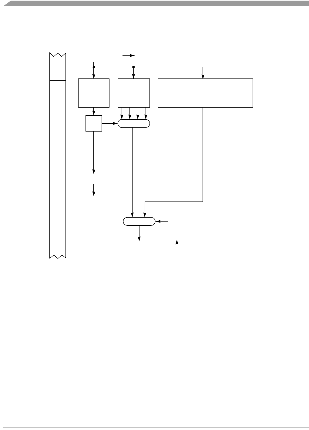
MCF548x Reference Manual, Rev. 3
5-20 Freescale Semiconductor
Figure 5-10 shows more details of the MMU structure. The TLB is accessed at the beginning of the KC1
pipeline stage so the resulting physical address can be sourced to the cache controllers to factor into the
cache hit/miss determination. This is required because caches are virtually indexed but physically mapped.
Figure 5-10. Address and Attributes Generation
5.6 MMU Implementation
The MMU implements a 64-entry full-associative Harvard TLB architecture with 32-entry ITLB and
DTLB. This section provides more details of this specific TLB implementation. This section details the
operation and looks at the size, frequency, miss rate, and miss recovery time of this specific TLB
implementation.
5.6.1 TLB Address Fields
Because the TLB has a total of 64 entries (32 each for the ITLB and DTLB), a 6-bit address field is
necessary. TLB addresses 0–31 reference the ITLB, and TLB addresses 32–63 reference the DTLB.
In the MMUOR, bits 0 through 5 of the TLB allocation address (AA[5–0]) have this address format for
CF4e. The remaining TLB allocation address bits (AA[15–6]) are ignored on updates and always read as
zero.
JADDR, J Control
TLB Hit
KADDR_KC1
entries
Comp
TLB tag entries
TLB data
entry
TLB hit
data
KC1
J
Memory unit access control
(MMUBAR, RAMBARs, ROMBARs,
ACRs, CACR priority hit logic)
Translated address
MMU’s access control
Untranslated address
mapping register’s
access control
KC1 cycle access control
Mapping register hit
or special mode access
To memory controllers
To control for TLB miss
logic
To control for TLB miss
logic
To memory controllers plus
bus interface

MMU Implementation
MCF548x Reference Manual, Rev. 3
Freescale Semiconductor 5-21
When MMUAR is used for a TLB address, bits FA[5–0] also have this address format for CF4e. The
remaining form address bits (FA[31–6]) are ignored when this register is being used for a TLB address.
5.6.2 TLB Replacement Algorithm
The instruction and data TLBs provide low-latency access to recently used instruction and operand
translation information. CF4e ITLBs and DTLBs are 32-entry fully associative caches. The 32 ITLB
entries are searched on each instruction reference; the 32 DTLB entries are searched on each operand
reference.
CF4e TLBs are software controlled. The TLB clear-all function clears valid bits on every TLB entry and
resets the replacement logic. A new valid entry is loaded in the TLBs may be designated as locked and
unavailable for allocation. TLB hits to locked entries do not update replacement algorithm information.
When a new TLB entry needs to be allocated, the user can specify the exact TLB entry to be updated
(through MMUOR[ADR] and MMUAR) or let TLB hardware pick the entry to update based on the
replacement algorithm. A pseudo-least-recently used (PLRU) algorithm picks the entry to be replaced on
a TLB miss. The algorithm works as follows:
• If any element is empty (non-valid), use the lowest empty element as the allocate entry (that is,
entry 0 before 1, 2, 3, and so on).
• If all entries are valid, use the entry indicated by the PLRU as the allocate entry.
The PLRU algorithm uses 31 most-recently used state bits per TLB to track the TLB hit history. Table 5-13
lists these state bits.
Table 5-13. PLRU State Bits
State Bits Meaning
rdRecent31To16 A one indicates 31To16 is more recent than 15To00
rdRecent31To24 A one indicates 31To24 is more recent than 23To16
rdRecent15To08 A one indicates 15To08 is more recent than 07To00
rdRecent31To28 A one indicates 31To28 is more recent than 27To24
rdRecent23To20 A one indicates 23To20 is more recent than 19To16
rdRecent15To12 A one indicates 15To12 is more recent than 11To08
rdRecent07To04 A one indicates 07To04 is more recent than 03To00
rdRecent31To30 A one indicates 31To30 is more recent than 29To28
rdRecent27To26 A one indicates 27To26 is more recent than 25To24
rdRecent23To22 A one indicates 23To22 is more recent than 21To20
rdRecent19To18 A one indicates 19To18 is more recent than 17To16
rdRecent15To14 A one indicates 15To14 is more recent than 13To12
rdRecent11To10 A one indicates 11To10 is more recent than 09To08
rdRecent07To06 A one indicates 07To06 is more recent than 05To04
rdRecent03To02 A one indicates 03To02 is more recent than 01To00
rdRecent31 A one indicates 31 is more recent than 30
rdRecent29 A one indicates 29 is more recent than 28

MCF548x Reference Manual, Rev. 3
5-22 Freescale Semiconductor
Binary state bits are updated on all TLB write (load) operations, as well as normal ITLB and DTLB hits
of non-locked entries. Also, if all entries in a binary state are locked, than that state is always set. That is,
if entries 15, 14, 13, and 12 were locked, LRU state bit rdRecent15To14 is forced to one.
For a completely valid TLB, binary state information determines the LRU entry. The CF4e replacement
algorithm is deterministic and, for the case of a full TLB (with no locked entries and always touching new
pages), the replacement entry repeats every 32 TLB loads.
5.6.3 TLB Locked Entries
Figure 5-11 is a ColdFire MMU Harvard TLB block diagram.
For TLB miss faults, the instruction restart model completely reexecutes an instruction on returning from
the exception handler. An instruction can touch two instruction pages (a 32- or 48-bit instruction can
straddle two pages) or four data pages (a memory-to-memory word or longword move where misaligned
source and destination operands straddle two pages). Therefore, one instruction may take two ITLB misses
and allocate two ITLB pages before completion. Likewise, one instruction may require four DTLB misses
and allocate four DTLB pages. Because of this, a pool of unlocked TLB entries must be available if virtual
memory is used.
The above examples show the fewest entries needed to guarantee an instruction can complete execution.
For good MMU performance, more unlocked TLB entries should be available.
rdRecent27 A one indicates 27 is more recent than 26
rdRecent25 A one indicates 25 is more recent than 24
rdRecent23 A one indicates 23 is more recent than 22
rdRecent21 A one indicates 21 is more recent than 20
rdRecent19 A one indicates 19 is more recent than 18
rdRecent17 A one indicates 17 is more recent than 16
rdRecent15 A one indicates 15 is more recent than 14
rdRecent13 A one indicates 13 is more recent than 12
rdRecent11 A one indicates 11 is more recent than 10
rdRecent09 A one indicates 09 is more recent than 08
rdRecent07 A one indicates 07 is more recent than 06
rdRecent05 A one indicates 05 is more recent than 04
rdRecent03 A one indicates 03 is more recent than 02
rdRecent01 A one indicates 01 is more recent than 00
Table 5-13. PLRU State Bits (Continued)
State Bits Meaning
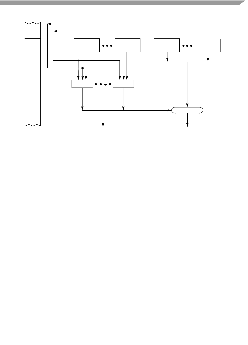
MMU Instructions
MCF548x Reference Manual, Rev. 3
Freescale Semiconductor 5-23
Figure 5-11. Version 4 ColdFire MMU Harvard TLB
5.7 MMU Instructions
The MOVE to USP and MOVE from USP instructions have been added for accessing the USP. Refer to
the ColdFire Programmer’s Reference Manual for more information.
KC1
J
Current address space ID (ASID)
Compare
IC1 or OC1 translated address
IC1 or OC1 access control
TLB Tag
Entry 31 TLB Tag
Entry 0 TLB Tag
Entry 31 TLB Tag
Entry 0
To control for instruction or DTLB miss
logic
Instruction or data hit select
Instruction or data address and attributes
Compare

MCF548x Reference Manual, Rev. 3
5-24 Freescale Semiconductor

MCF548x Reference Manual, Rev. 3
Freescale Semiconductor 6-1
Chapter 6
Floating-Point Unit (FPU)
6.1 Introduction
This chapter describes instructions implemented in the floating-point unit (FPU) designed for use with the
ColdFire family of microprocessors. The FPU conforms to the American National Standards Institute
(ANSI)/Institute of Electrical and Electronics Engineers (IEEE) Standard for Binary Floating-Point
Arithmetic (ANSI/IEEE Standard 754).
The hardware unit is optimized for real-time execution with exceptions disabled and default results
provided for specific operations, operands, and number types. The FPU does not support all IEEE-754
number types and operations in hardware. Exceptions can be enabled to support these cases in software.
6.1.1 Overview
The FPU operates on 64-bit, double-precision, floating-point data and supports single-precision and signed
integer input operands. The FPU programming model is like that in the MC68060 microprocessor. The
FPU is intended to accelerate the performance of certain classes of embedded applications, especially
those requiring high-speed floating-point arithmetic computations. See Section 6.7.3, “Key Differences
between ColdFire and M68000 FPU Programming Models.”
The FPU appears as another execute engine at the bottom stages of the operand execution pipeline (OEP),
using operands from a dual-ported register file.
Setting bit 4 in the cache control register (CACR[DF]) disables the FPU. If CACR[DF] is cleared, all FPU
instructions are issued and executed, otherwise the processor responds with an unimplemented line-F
instruction exception (vector 11).
Operating systems often assume user applications are integer-only (to minimize the time required by save
context) by setting CACR[DF] at process initiation. If the application includes floating-point instructions,
the attempted execution of the first FP instruction generates the unimplemented line-F exception, which
signals the kernel that the FPU registers must be included in the context for the application. The application
then continues execution with CACR[DF] cleared to enable FPU execution.
6.1.1.1 Notational Conventions
Table 6-1 defines notational conventions used in this chapter.
Table 6-1. Notational Conventions
Symbol Description
Single- and Double-Precision Operand Operations
+Arithmetic addition or postincrement indicator
−Arithmetic subtraction or predecrement indicator
×Arithmetic multiplication
÷Arithmetic division or conjunction symbol
∼Invert, operand is logically complemented. An overbar, , is also used for this operation.

MCF548x Reference Manual, Rev. 3
6-2 Freescale Semiconductor
Table 6-2 describes addressing modes and syntax for floating-point instructions.
&Logical AND
|Logical OR
→Source operand is moved to destination operand
<op> Any double-operand operation
<operand>tested Operand is compared to zero and the condition codes are set appropriately
sign-extended All bits of the upper portion are made equal to the high-order bit of the lower portion
Other Operations
If <condition>
then <operations>
else <operations>
Test the condition. If true, the operations after then are performed. If the condition is false and the
optional else clause is present, the operations after else are performed. If the condition is false
and else is omitted, the instruction performs no operation. Refer to the Bcc instruction description
as an example.
Register Specifications
An Address register n (example: A3 is address register 3)
Ay, Ax Source and destination address registers, respectively
Dn Data register n (example: D3 is data register 3)
Dy,Dx Source and destination data registers, respectively
FPCR Floating-point control register
FPIAR Floating-point instruction address register
FPn Floating-point data register n (example: FP3 is FPU data register 3)
FPSR Floating-point status register
FPy,FPx Source and destination floating-point data registers, respectively
PC Program counter
Rn Address or data register
Rx Destination register
Ry Source register
Xi Index register
Table 6-1. Notational Conventions (Continued)
Symbol Description

Operand Data Formats and Types
MCF548x Reference Manual, Rev. 3
Freescale Semiconductor 6-3
6.2 Operand Data Formats and Types
The FPU supports signed byte, word, and longword integer formats, which are identical to those supported
by the integer unit. The FPU also supports single- and double-precision binary floating-point formats that
fully comply with the IEEE-754 standard.
6.2.1 Signed-Integer Data Formats
The FPU supports 8-bit byte (B), 16-bit word (W), and 32-bit longword (L) integer data formats.
6.2.2 Floating-Point Data Formats
Figure 6-1 shows the two binary floating-point data formats.
Figure 6-1. Floating-Point Data Formats
Note that, throughout this chapter, a mantissa is defined as the concatenation of an integer bit, the binary
point, and a fraction. A fraction is the term designating the bits to the right of the binary point in the
mantissa.
Figure 6-2. Mantissa
The integer bit is implied to be set for normalized numbers and infinities, clear for zeros and denormalized
numbers. For not-a-numbers (NANs), the integer bit is ignored. The exponent in both floating-point
formats is an unsigned binary integer with an implied bias added to it. Subtracting the bias from exponent
Table 6-2. Floating-Point Addressing Modes
Addressing Modes Syntax
Register direct
Address register direct
Address register direct
Dy
Ay
Register indirect
Address register indirect
Address register indirect with postincrement
Address register indirect with predecrement
Address register indirect with displacement
(Ay)
–(Ay)
(d16,Ay)
Program counter indirect with displacement (d16,PC)
11-Bit Exponent
S52-Bit Fraction
62 51 0
Sign of Mantissa
0
23-Bit Fraction8-Bit Exponent
S
Sign of Mantissa
2230
Single
Double
31
63
(integer bit).(fraction)
Mantissa

MCF548x Reference Manual, Rev. 3
6-4 Freescale Semiconductor
yields a signed, two’s complement power of two. This represents the magnitude of a normalized
floating-point number when multiplied by the mantissa.
By definition, a normalized mantissa always takes values starting from 1.0 and going up to, but not
including, 2.0; that is, [1.0...2.0).
6.2.3 Floating-Point Data Types
Each floating-point data format supports five unique data types: normalized numbers, zeros, infinities,
NANs, and denormalized numbers. The normalized data type, Figure 6-3, never uses the maximum or
minimum exponent value for a given format.
6.2.3.1 Normalized Numbers
Normalized numbers include all positive or negative numbers with exponents between the maximum and
minimum values. For single- and double-precision normalized numbers, the implied integer bit is one and
the exponent can be zero.
Figure 6-3. Normalized Number Format
6.2.3.2 Zeros
Zeros can be positive or negative and represent real values, + 0.0 and – 0.0. See Figure 6-4.
Figure 6-4. Zero Format
6.2.3.3 Infinities
Infinities can be positive or negative and represent real values that exceed the overflow threshold. A
result’s exponent greater than or equal to the maximum exponent value indicates an overflow for a given
data format and operation. This overflow description ignores the effects of rounding and the
user-selectable rounding models. For single- and double-precision infinities, the fraction is a zero. See
Figure 6-5.
Figure 6-5. Infinity Format
Min < Exponent < Max Fraction = Any bit pattern
Sign of Mantissa, 0 or 1
Exponent = 0 Fraction = 0
Sign of Mantissa, 0 or 1
Exponent = Maximum Fraction = 0
Sign of Mantissa, 0 or 1

Operand Data Formats and Types
MCF548x Reference Manual, Rev. 3
Freescale Semiconductor 6-5
6.2.3.4 Not-A-Number
When created by the FPU, NANs represent the results of operations having no mathematical interpretation,
such as infinity divided by infinity. Operations using a NAN operand as an input return a NAN result.
User-created NANs can protect against uninitialized variables and arrays or can represent user-defined
data types. See Figure 6-6.
Figure 6-6. Not-a-Number Format
If an input operand to an operation is a NAN, the result is an FPU-created default NAN. When the FPU
creates a NAN, the NAN always contains the same bit pattern in the fraction: all fraction bits are ones and
the sign bit is zero. When the user creates a NAN, any nonzero bit pattern can be stored in the fraction and
the sign bit.
6.2.3.5 Denormalized Numbers
Denormalized numbers represent real values near the underflow threshold. Denormalized numbers can be
positive or negative. For denormalized numbers in single- and double-precision, the implied integer bit is
a zero. See Figure 6-7.
Figure 6-7. Denormalized Number Format
Traditionally, the detection of underflow causes floating-point number systems to perform a flush-to-zero.
The IEEE-754 standard implements gradual underflow: the result mantissa is shifted right (denormalized)
while the result exponent is incremented until reaching the minimum value. If all the mantissa bits of the
result are shifted off to the right during this denormalization, the result becomes zero.
Denormalized numbers are not supported directly in the hardware of this implementation but can be
handled in software if needed (software for the input denorm exception could be written to handle
denormalized input operands, and software for the underflow exception could create denormalized
numbers). If the input denorm exception is disabled, all denormalized numbers are treated as zeros.
Table 6-3 summarizes the data type specifications for byte, word, longword, single- and double-precision
data formats.
Table 6-3. Real Format Summary
Parameter Single-Precision Double-Precision
Data Format
Field Size in Bits
Sign (s) 1 1
Exponent = Maximum Fraction = Any nonzero bit pattern
Sign of Mantissa, 0 or 1
Exponent = 0 Fraction = Any nonzero bit pattern
Sign of Mantissa, 0 or 1
se f
3130 23 22 0
se f
6362 52 51 0

MCF548x Reference Manual, Rev. 3
6-6 Freescale Semiconductor
Biased exponent (e) 8 11
Fraction (f) 23 52
Total 32 64
Interpretation of Sign
Positive fraction s = 0 s = 0
Negative fraction s = 1 s = 1
Normalized Numbers
Bias of biased exponent +127 (0x7F) +1023 (0x3FF)
Range of biased exponent 0 < e < 255 (0xFF) 0 < e < 2047 (0x7FF)
Range of fraction Zero or Nonzero Zero or Nonzero
Mantissa 1.f 1.f
Relation to representation of real numbers (–1)s × 2e–127 × 1.f (–1)s × 2e–1023 × 1.f
Denormalized Numbers
Biased exponent format minimum 0 (0x00) 0 (0x000)
Bias of biased exponent +126 (0x7E) +1022 (0x3FE)
Range of fraction Nonzero Nonzero
Mantissa 0.f 0.f
Relation to representation of real numbers (–1)s × 2–126 × 0.f (–1)s × 2–1022 × 0.f
Signed Zeros
Biased exponent format minimum 0 (0x00) 0 (0x00)
Mantissa 0.f = 0.0 0.f = 0.0
Signed Infinities
Biased exponent format maximum 255 (0xFF) 2047 (0x7FF)
Mantissa 0.f = 0.0 0.f = 0.0
NANs
Sign Don’t Care 0 or 1
Biased exponent format maximum 255 (0xFF) 2047 (0x7FF)
Fraction Nonzero Nonzero
Representation of Fraction
Nonzero Bit Pattern Created by User
Fraction When Created by FPU
xxxxx…xxxx
11111…1111
xxxxx…xxxx
11111…1111
Table 6-3. Real Format Summary (Continued)
Parameter Single-Precision Double-Precision

Register Definition
MCF548x Reference Manual, Rev. 3
Freescale Semiconductor 6-7
6.3 Register Definition
The programmer’s model for the FPU consists of the following:
• Eight 64-bit floating-point data registers (FP0–FP7)
• One 32-bit floating-point control register (FPCR)
• One 32-bit floating-point status register (FPSR)
• One 32-bit floating-point instruction address register (FPIAR)
Figure 6-8 shows the FPU programming model.
Figure 6-8. Floating-Point Programmer’s Model
6.3.1 Floating-Point Data Registers (FP0–FP7)
Floating-point data registers are analogous to the integer data registers for the 68K/ColdFire family. They
always contain numbers in double-precision format, even though the operand may be a single-precision
value used in a single-precision calculation. All external operands, regardless of the source data format,
are converted to double-precision format before being used in any calculation or being stored in a
floating-point data register. A reset or a null-restore operation sets FP0–FP7 to positive, nonsignaling
NANs.
6.3.2 Floating-Point Control Register (FPCR)
The FPCR, Figure 6-9, contains an exception enable byte (EE) and a mode control byte (MC). Each EE
bit corresponds to a floating-point exception class. The user can separately enable traps for each class of
floating-point exceptions. The MC bits control FPU operating modes.
Approximate Ranges
Maximum Positive Normalized 3.4 × 1038 1.8 x 10308
Minimum Positive Normalized 1.2 × 10–38 2.2 x 10–308
Minimum Positive Denormalized 1.4 × 10–45 4.9 x 10–324
63 0
FP0 Floating-point data registers
FP1
FP2
FP3
FP4
FP5
FP6
FP7
FPCR Floating-point control register
FPSR Floating-point status register
FPIAR Floating-point instruction address register
Table 6-3. Real Format Summary (Continued)
Parameter Single-Precision Double-Precision

MCF548x Reference Manual, Rev. 3
6-8 Freescale Semiconductor
The user can read or write to FPCR using FMOVE or FRESTORE. A processor reset or a restore operation
of the null state clears the FPCR. When this register is cleared, the FPU never generates exceptions.
Table 6-4 describes FPCR fields.
31 30 29 28 27 26 25 24 23 22 21 20 19 18 17 16
R0 0 0 000000000000 0
W
Reset0 0 0 000000000000 0
15 14 13 12 11 10 9 8 7 6 5 4 3 2 1 0
Exception Enable Byte (EE) Mode Control Byte (MC)
R BSUN INAN OPERR OVFL UNFL DZ INEX IDE 0 PREC RND 0 0 0 0
W
Reset0 0 0 000000000000 0
Reg
Addr
CPU + 0x824
Figure 6-9. Floating-Point Control Register (FPCR)
Table 6-4. FPCR Field Descriptions
Bits Field Description
31–16 — Reserved, should be cleared.
15 BSUN Branch set on unordered
14 INAN Input not-a-number
13 OPERR Operand error
12 OVFL Overflow
11 UNFL Underflow
10 DZ Divide by zero
9 INEX Inexact operation
8 IDE Input denormalized
7 — Reserved, should be cleared.
6 PREC Rounding precision
0 Double (D)
1Single (S)
5–4 RND Rounding mode
00 To nearest (RN)
01 To zero (RZ)
10 To minus infinity (RM)
11 To plus infinity (RP)
3–0 — Reserved, should be cleared.

Register Definition
MCF548x Reference Manual, Rev. 3
Freescale Semiconductor 6-9
6.3.3 Floating-Point Status Register (FPSR)
The FPSR, Figure 6-10, contains a floating-point condition code byte (FPCC), a floating-point exception
status byte (EXC), and a floating-point accrued exception byte (AEXC). The user can read or write all
FPSR bits. Execution of most floating-point instructions modifies FPSR. FPSR is loaded using FMOVE
or FRESTORE. A processor reset or a restore operation of the null state clears the FPSR.
The floating-point condition code byte contains 4 condition code bits that are set after completion of all
arithmetic instructions involving the floating-point data registers. The floating-point store operation,
FMOVEM, and move system control register instructions do not affect the FPCC.
The exception status byte contains a bit for each floating-point exception that might have occurred during
the most recent arithmetic instruction or move operation. This byte is cleared at the start of all operations
that generate floating-point exceptions (except FBcc only affects BSUN and that only for nonaware tests).
Operations that do not generate floating-point exceptions do not clear this byte. An exception handler can
use this byte to determine which floating-point exception or exceptions caused a trap. The equations below
the table show the comparative relationship between the EXC byte and AEXC byte.
The accrued exception byte contains 5 required bits for IEEE-754 exception-disabled operations. These
exceptions are logical combinations of EXC bits. AEXC records all floating-point exceptions since AEXC
was last cleared, either by writing to FPSR or as a result of reset or a restore operation of the null state.
Many users disable traps for some or all floating-point exception classes. AEXC eliminates the need to
poll EXC after each floating-point instruction. At the end of arithmetic operations, EXC bits are logically
combined to form an AEXC value that is logically ORed into the existing AEXC byte (FBcc only updates
IOP). This operation creates sticky floating-point exception bits in AEXC that the user can poll only at the
end of a series of floating-point operations. A sticky bit is one that remains set until the user clears it.
Setting or clearing AEXC bits neither causes nor prevents an exception. The equations below the table
show relationships between EXC and AEXC. Comparing the current value of an AEXC bit with a
combination of EXC bits derives a new value in the corresponding AEXC bit. These boolean equations
apply to setting AEXC bits at the end of each operation affecting AEXC.
Table 6-5 describes FPSR fields.
31 30 29 28 27 26 25 24 23 22 21 20 19 18 17 16
Floating-Point Condition Code Byte (FPCC)
R0 0 0 0 N Z INAN0 0 0 0 0 0 0 0
W
Reset 0 0 0 0 0 0 0 0 0 0 0 0 0 0 0 0
15 14 13 12 11 10 9 8 7 6 5 4 3 2 1 0
Exception Status Byte (EXC) Floating-Point Accrued Exception Byte (AEXC)
R BSUN INAN OPERR OVFL UNFL DZ INEX IDE IOP OVFL UNFL DZ INEX 0 0 0
W
Reset 0 0 0 0 0 0 0 0 0 0 0 0 0 0 0 0
Reg
Addr
CPU + 0x822
Figure 6-10. Floating-Point Status Register (FPSR)

MCF548x Reference Manual, Rev. 3
6-10 Freescale Semiconductor
For AEXC[OVFL], AEXC[DZ], and AEXC[INEX], the next value is determined by ORing the current
AEXC value with the EXC equivalent, as shown in the following:
• Next AEXC[OVFL] = Current AEXC[OVFL] | EXC[OVFL]
• Next AEXC[DZ] = Current AEXC[DZ] | EXC[DZ]
• Next AEXC[INEX] = Current AEXC[INEX] | EXC[INEX]
For AEXC[IOP] and AEXC[UNFL], the next value is calculated by ORing the current AEXC value with
EXC bit combinations, as follows:
• Next AEXC[IOP] = Current AEXC[IOP] | EXC[BSUN | INAN | OPERR]
• Next AEXC[UNFL] = Current AEXC[UNFL] | EXC[UNFL & INEX]
6.3.4 Floating-Point Instruction Address Register (FPIAR)
The ColdFire OEP can execute integer and floating-point instructions simultaneously. As a result, the PC
value stacked by the processor in response to a floating-point exception trap may not point to the
instruction that caused the exception.
Table 6-5. FPSR Field Descriptions
Bits Field Description
31–28 — Reserved, should be cleared.
27 N Negative
26 Z Zero
25 I Infinity
24 NAN Not-a-number
23–16 — Reserved, should be cleared.
15 BSUN Branch/set on unordered
14 INAN Input not-a-number
13 OPERR Operand error
12 OVFL Overflow
11 UNFL Underflow
10 DZ Divide by zero
9 INEX Inexact result
8 IDE Input is denormalized
7 IOP Invalid operation
6OVFLOverflow
5 UNFL Underflow
4 DZ Divide by zero
3 INEX Inexact result
2–0 — Reserved, should be cleared.

Floating-Point Computational Accuracy
MCF548x Reference Manual, Rev. 3
Freescale Semiconductor 6-11
For FPU instructions that can generate exception traps, the 32-bit FPIAR is loaded with the instruction PC
address before the FPU begins execution. In case of an FPU exception, the trap handler can use the FPIAR
contents to determine the instruction that generated the exception. FMOVE to/from FPCR, FPSR, or
FPIAR and FMOVEM instructions cannot generate floating-point exceptions; therefore, they do not
modify FPIAR. A reset or a null-restore operation clears FPIAR.
6.4 Floating-Point Computational Accuracy
The FPU performs all floating-point internal operations in double-precision. It supports mixed-mode
arithmetic by converting single-precision operands to double-precision values before performing the
specified operation. The FPU converts all memory data formats to the double-precision data format and
stores the value in a floating-point register or uses it as the source operand for an arithmetic operation.
When moving a double-precision floating-point value from a floating-point data register, the FPU can
convert the data depending on the destination, as follows:
• Valid data formats for memory destination: B, W, L, S, or D
• Valid data formats for integer data register destinations: B, W, L, or S
Normally if the input operand is a denormalized number, the number must be normalized before an FPU
instruction can be executed. A denormalized input operand is converted to zero if the input denorm
exception (IDE) is disabled. If IDE is enabled, the floating-point engine traps to allow software action to
be taken by the handler.
6.4.1 Intermediate Result
All FPU calculations use an intermediate result. When the FPU performs any operation, the calculation is
carried out using double-precision inputs, and the intermediate result is calculated as if to produce infinite
precision. After the calculation is complete, any necessary rounding of the intermediate result for the
selected precision is performed and the result is stored in the destination.
Figure 6-11 shows the intermediate result format. The intermediate result’s exponent for some dyadic
operations (for example, multiply and divide) can easily overflow or underflow the 11-bit exponent of the
designated floating-point register. To simplify overflow and underflow detection, intermediate results in
the FPU maintain a 12-bit two’s complement, integer exponent. Detection of an intermediate result
overflow or underflow always converts the 12-bit exponent into a 11-bit biased exponent before being
stored in a floating-point data register. The FPU internally maintains a 56-bit mantissa for rounding
purposes. The mantissa is always rounded to 53 bits (or fewer, depending on the selected rounding
precision) before it is stored in a floating-point data register.
Figure 6-11. Intermediate Result Format
If the destination is a floating-point data register, the result is in double-precision format but may be
rounded to single-precision, if required by the rounding precision, before being stored. If the
single-precision mode is selected, the exponent value is in the correct range even if it is stored in
52-Bit Fraction
Integer lsb
Guard
Sticky
Round
12-Bit Exponent
56-Bit Intermediate Mantissa

MCF548x Reference Manual, Rev. 3
6-12 Freescale Semiconductor
double-precision format. If the destination is a memory location or an integer data register, rounding
precision is ignored. In this case, a number in the double-precision format is taken from the source
floating-point data register, rounded to the destination format precision, and then written to memory or the
integer data register.
Depending on the selected rounding mode or destination data format, the location of the lsb of the mantissa
and the locations of the guard, round, and sticky bits in the 56-bit intermediate result mantissa vary. Guard
and round bits are calculated exactly. The sticky bit creates the illusion of an infinitely wide intermediate
result. As the arrow in Figure 6-11 shows, the sticky bit is the logical OR of all bits to the right of the round
bit in the infinitely precise result. During calculation, nonzero bits generated to the right of the round bit
set the sticky bit. Because of the sticky bit, the rounded intermediate result for all required IEEE arithmetic
operations in RN mode can err by no more than one half unit in the last place.
6.4.2 Rounding the Result
The FPU supports the four rounding modes specified by the IEEE-754 standard: round-to-nearest (RN),
round-toward-zero (RZ), round-toward-plus-infinity (RP), and round-toward-minus-infinity (RM). The
RM and RP modes are often referred to as directed-rounding-modes and are useful in interval arithmetic.
Rounding is accomplished through the intermediate result. Single-precision results are rounded to a 24-bit
mantissa boundary; double-precision results are rounded to a 53-bit mantissa boundary.
The current floating-point instruction can specify rounding precision, overriding the rounding precision
specified in FPCR for the duration of the current instruction. For example, the rounding precision for
FADD is determined by FPCR, while the rounding precision for FSADD is single-precision, independent
of FPCR.
Range control helps emulate devices that support only single-precision arithmetic by rounding the
intermediate result’s mantissa to the specified precision and checking that the intermediate exponent is in
the representable range of the selected rounding precision. If the intermediate result’s exponent exceeds
the range, the appropriate underflow or overflow value is stored as the result in the double-precision format
exponent. For example, if the data format and rounding mode is single-precision RM and the result of an
arithmetic operation overflows the single-precision format, the maximum normalized single-precision
value is stored as a double-precision number in the destination floating-point data register; that is, the
unbiased 11-bit exponent is 0x0FF and the 52-bit fraction is 0xF_FFFF_E000_0000. If an infinity is the
appropriate result for an underflow or overflow, the infinity value for the destination data format is stored
as the result; that is, the exponent has the maximum value and the mantissa is zero.
Figure 6-12 shows the algorithm for rounding an intermediate result to the selected rounding precision and
destination data format. If the destination is a floating-point register, the rounding boundary is determined
by either the selected rounding precision specified by FPCR[PREC] or by the instruction itself. For
example, FSADD and FDADD specify single- and double-precision rounding regardless of FPCR[PREC].
If the destination is memory or an integer data register, the destination data format determines the rounding
boundary. If the rounded result of an operation is inexact, INEX is set in FPSR[EXC].
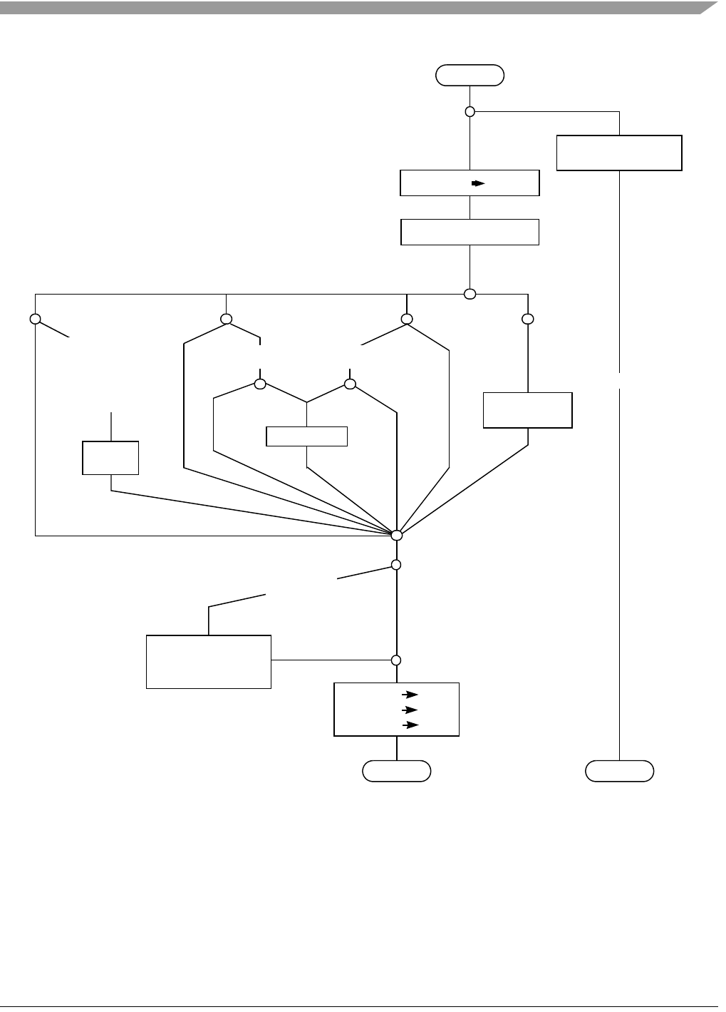
Floating-Point Computational Accuracy
MCF548x Reference Manual, Rev. 3
Freescale Semiconductor 6-13
Figure 6-12. Rounding Algorithm Flowchart
The 3 additional bits beyond the double-precision format, the difference between the intermediate result’s
56-bit mantissa and the storing result’s 53-bit mantissa, allow the FPU to perform all calculations as
though it were performing calculations using a compute engine with infinite bit precision. The result is
always correct for the specified destination’s data format before rounding (unless an overflow or
underflow error occurs). The specified rounding produces a number as close as possible to the infinitely
precise intermediate value and still representable in the selected precision. The tie case in Table 6-6 shows
how the 56-bit mantissa allows the FPU to meet the error bound of the IEEE specification.
INEX 1
Select Rounding Mode
Guard, Round
and Sticky Bits = 0
Exact Result
G,R, and S
are chopped
RZ
Check Intermediate Result
RPRMRN
NegPos
NegPos
Add 1 to
lsb
G and lsb = 1,
R and S = 0
or
G = 1,
R or S = 1
Shift mantissa
right 1 bit,
Add 1 to exponent
Overflow = 1
Guard 0
Round 0
Sticky 0
Exit Exit
Entry
NY
G, R,
or S = 1
Add 1 to lsb
G, R,
or S = 1
YN

MCF548x Reference Manual, Rev. 3
6-14 Freescale Semiconductor
The lsb of the rounded result does not increment even though the guard bit is set in the intermediate result.
The IEEE-754 standard specifies this way of handling ties. If the destination data format is
double-precision and there is a difference between the infinitely precise intermediate result and the
round-to-nearest result, the relative difference is 2–53 (the value of the guard bit). This error is equal to half
of the lsb’s value and is the worst case error that can be introduced with RN mode. Thus, the term one-half
unit in the last place correctly identifies the error bound for this operation. This error specification is the
relative error present in the result; the absolute error bound is equal to 2exponent x 2–53. Table 6-7 shows
the error bound for other rounding modes.
The difference between the infinitely precise result and the rounded result is 2–53 + 2–54 + 2–55, which is
slightly less than 2–52 (the value of the lsb). Thus, the error bound for this operation is not more than one
unit in the last place. The FPU meets these error bounds for all arithmetic operations, providing accurate,
repeatable results.
6.5 Floating-Point Post-Processing
Most operations end with post-processing, for which the FPU provides two steps. First, FPSR[FPCC] bits
are set or cleared at the end of each arithmetic or move operation to a single floating-point data register.
FPCC bits are consistently set based on the result of the operation. Second, the FPU supports 32
conditional tests that allow floating-point conditional instructions to test floating-point conditions in the
same way that integer conditional instructions test the integer condition code. The combination of
consistently set FPCC bits and the simple programming of conditional instructions gives the processor a
highly flexible, efficient way to change program flow based on floating-point results. When the summary
for each instruction is read, it should be assumed that an instruction performs post processing, unless the
summary specifically states otherwise. The following paragraphs describe post processing in detail.
6.5.1 Underflow, Round, and Overflow
During calculation of an arithmetic result, the FPU has more precision and range than the 64-bit
double-precision format. However, the final result is a double-precision value. In some cases, an
intermediate result becomes either smaller or larger than can be represented in double-precision. Also, the
operation can generate a larger exponent or more bits of precision than can be represented in the chosen
rounding precision. For these reasons, every arithmetic instruction ends by checking for underflow,
rounding the result and checking for overflow.
At the completion of an arithmetic operation, the intermediate result is checked to see if it is too small to
be represented as a normalized number in the selected precision. If so, the underflow (UNFL) bit is set in
FPSR[EXC]. If no underflow occurs, the intermediate result is rounded according to the user-selected
Table 6-6. Tie-Case Example
Result Integer 52-Bit Fraction Guard Round Sticky
Intermediate x xxx…x00 1 0 0
Rounded-to-Nearest x xxx…x00 0 0 0
Table 6-7. Round Mode Error Bounds
Result Integer 52-Bit Fraction Guard Round Sticky
Intermediate x xxx…x00 1 1 1
Rounded-to-Zero x xxx…x00 0 0 0

Floating-Point Post-Processing
MCF548x Reference Manual, Rev. 3
Freescale Semiconductor 6-15
rounding precision and mode. After rounding, the inexact bit (INEX) is set as described in Figure 6-12.
Lastly, the magnitude of the result is checked to see if it exceeds the current rounding precision. If so, the
overflow (OVFL) bit is set, and a correctly signed infinity or correctly signed largest normalized number
is returned, depending on the rounding mode.
NOTE
INEX can also be set by OVFL, UNFL, and when denormalized numbers
are encountered.
6.5.2 Conditional Testing
Unlike operation-dependent integer condition codes, an instruction either always sets FPCC bits in the
same way or does not change them at all. Therefore, instruction descriptions do not include FPCC settings.
This section describes how FPCC bits are set.
FPCC bits differ slightly from integer condition codes. An FPU operation’s final result sets or clears FPCC
bits accordingly, independent of the operation itself. Integer condition code bits N and Z have this
characteristic, but V and C are set differently for different instructions. Table 6-8 lists FPCC settings for
each data type. Loading FPCC with another combination and executing a conditional instruction can
produce an unexpected branch condition.
The inclusion of the NAN data type in the IEEE floating-point number system requires each conditional
test to include FPCC[NAN] in its boolean equation. Because it cannot be determined whether a NAN is
bigger or smaller than an in-range number (since it is unordered), the compare instruction sets
FPCC[NAN] when an unordered compare is attempted. All arithmetic instructions that result in a NAN
also set the NAN bit. Conditional instructions interpret NAN being set as the unordered condition.
The IEEE-754 standard defines the following four conditions:
• Equal to (EQ)
• Greater than (GT)
•Less than (LT)
• Unordered (UN)
The standard requires only the generation of the condition codes as a result of a floating-point compare
operation. The FPU can test for these conditions and 28 others at the end of any operation affecting
condition codes. For floating-point conditional branch instructions, the processor logically combines the
4 bits of the FPCC condition codes to form 32 conditional tests, 16 of which cause an exception if an
Table 6-8. FPCC Encodings
Data Type N Z I NAN
+ Normalized or Denormalized0000
– Normalized or Denormalized1000
+ 0 0100
– 0 1100
+ Infinity 0010
– Infinity 1010
+ NAN 0001
– NAN 1001

MCF548x Reference Manual, Rev. 3
6-16 Freescale Semiconductor
unordered condition is present when the conditional test is attempted (IEEE nonaware tests). The other 16
do not cause an exception (IEEE-aware tests). The set of IEEE nonaware tests is best used in one of the
following cases:
• When porting a program from a system that does not support the IEEE standard to a conforming
system
• When generating high-level language code that does not support IEEE floating-point concepts (that
is, the unordered condition).
An unordered condition occurs when one or both of the operands in a floating-point compare operation is
a NAN. The inclusion of the unordered condition in floating-point branches destroys the familiar
trichotomy relationship (greater than, equal, less than) that exists for integers. For example, the opposite
of floating-point branch greater than (FBGT) is not floating-point branch less than or equal (FBLE).
Rather, the opposite condition is floating-point branch not greater than (FBNGT). If the result of the
previous instruction was unordered, FBNGT is true, whereas both FBGT and FBLE would be false because
unordered fails both of these tests (and sets BSUN). Compiler code generators should be particularly
careful of the lack of trichotomy in the floating-point branches, because it is common for compilers to
invert the sense of conditions.
When using the IEEE nonaware tests, the user receives a BSUN exception if a branch is attempted and
FPCC[NAN] is set, unless the branch is an FBEQ or an FBNE. If the BSUN exception is enabled in FPCR,
the exception takes a BSUN trap. Therefore, the IEEE nonaware program is interrupted if an unexpected
condition occurs. Users knowledgeable of the IEEE-754 standard should use IEEE-aware tests in
programs that contain ordered and unordered conditions. Because the ordered or unordered attribute is
explicitly included in the conditional test, EXC[BSUN] is not set when the unordered condition occurs.
Table 6-9 summarizes conditional mnemonics, definitions, equations, predicates, and whether
EXC[BSUN] is set for the 32 floating-point conditional tests. The equation column lists FPCC bit
combinations for each test in the form of an equation. Condition codes with an overbar indicate cleared
bits; all other bits are set.
Table 6-9. Floating-Point Conditional Tests
Mnemonic Definition Equation Predicate 1EXC[BSUN] Set
IEEE Nonaware Tests
EQ Equal Z 000001 No
NE Not equal Z 001110 No
GT Greater than NAN | Z | N 010010 Yes
NGT Not greater than NAN | Z | N 011101 Yes
GE Greater than or equal Z | (NAN | N) 010011 Yes
NGE Not greater than or equal NAN | (N & Z) 011100 Yes
LT Less than N & (NAN | Z) 010100 Yes
NLT Not less than NAN | (Z | N) 011011 Yes
LE Less than or equal Z | (N & NAN) 010101 Yes
NLE Not less than or equal NAN | (N | Z) 011010 Yes
GL Greater or less than NAN | Z 010110 Yes
NGL Not greater or less than NAN | Z 011001 Yes
GLE Greater, less or equal NAN 010111 Yes
Floating-Point Exceptions
MCF548x Reference Manual, Rev. 3
Freescale Semiconductor 6-17
6.6 Floating-Point Exceptions
This section describes floating-point exceptions and how they are handled. Table 6-10 lists the vector
numbers related to floating-point exceptions. If the exception is taken pre-instruction, the PC contains the
address of the next floating-point instruction (nextFP). If the exception is taken post-instruction, the PC
contains the address of the faulting instruction (fault).
NGLE Not greater, less or equal NAN 011000 Yes
IEEE-Aware Tests
EQ Equal Z 000001 No
NE Not equal Z 001110 No
OGT Ordered greater than NAN | Z | N 000010 No
ULE Unordered or less or equal NAN | Z | N 001101 No
OGE Ordered greater than or equal Z | (NAN | N) 000011 No
ULT Unordered or less than NAN | (N & Z) 001100 No
OLT Ordered less than N & (NAN | Z) 000100 No
UGE Unordered or greater or equal NAN | (Z | N) 001011 No
OLE Ordered less than or equal Z | (N & NAN) 000101 No
UGT Unordered or greater than NAN | (N | Z) 001010 No
OGL Ordered greater or less than NAN | Z 000110 No
UEQ Unordered or equal NAN | Z 001001 No
OR Ordered NAN 000111 No
UN Unordered NAN 001000 No
Miscellaneous Tests
F False False 000000 No
T True True 001111 No
SF Signaling false False 010000 Yes
ST Signaling true True 011111 Yes
SEQ Signaling equal Z 010001 Yes
SNE Signaling not equal Z 011110 Yes
1This column refers to the value in the instruction’s conditional predicate field that specifies this test.
Table 6-9. Floating-Point Conditional Tests (Continued)
Mnemonic Definition Equation Predicate 1EXC[BSUN] Set

MCF548x Reference Manual, Rev. 3
6-18 Freescale Semiconductor
In addition to these vectors, attempting to execute a FRESTORE instruction with a unsupported frame
value generates a format error exception (vector 14). See the FRESTORE instruction in the ColdFire
Programmer’s Reference Manual.
Attempting to execute an FPU instruction with an undefined or unsupported value in the 6-bit effective
address, the 3-bit source/destination specifier, or the 7-bit opmode generates a line-F emulator exception,
vector 11. See Table 6-23.
6.6.1 Floating-Point Arithmetic Exceptions
This section describes floating-point arithmetic exceptions; Table 6-11 lists these exceptions in order of
priority:
Most floating-point exceptions are taken when the next floating-point arithmetic instruction is encountered
(this is called a pre-instruction exception). Exceptions set during a floating-point store to memory or to an
integer register are taken immediately (post-instruction exception).
Note that FMOVE is considered an arithmetic instruction because the result is rounded. Only FMOVE
with any destination other than a floating-point register (sometimes called FMOVE OUT) can generate
post-instruction exceptions. Post-instruction exceptions never write the destination. After a
post-instruction exception, processing continues with the next instruction.
Table 6-10. Floating-Point Exception Vectors
Vector Number Vector Offset Program Counter Assignment
48 0x0C0 Fault Floating-point branch/set on unordered condition
49 0x0C4 NextFP or Fault Floating-point inexact result
50 0x0C8 NextFP Floating-point divide-by-zero
51 0x0CC NextFP or Fault Floating-point underflow
52 0x0D0 NextFP or Fault Floating-point operand error
53 0x0D4 NextFP or Fault Floating-point overflow
54 0x0D8 NextFP or Fault Floating-point input NAN
55 0x0DC NextFP or Fault Floating-point input denormalized number
Table 6-11. Exception Priorities
Priority Exception
1 Branch/set on unordered (BSUN)
2 Input Not-a-Number (INAN)
3 Input denormalized number (IDE)
4 Operand error (OPERR)
5Overflow (OVFL)
6 Underflow (UNFL)
7 Divide-by-zero (DZ)
8 Inexact (INEX)

Floating-Point Exceptions
MCF548x Reference Manual, Rev. 3
Freescale Semiconductor 6-19
A floating-point arithmetic exception becomes pending when the result of a floating-point instruction sets
an FPSR[EXC] bit and the corresponding FPCR[ENABLE] bit is set. A user write to the FPSR or FPCR
that causes the setting of an exception bit in FPSR[EXC] along with its corresponding exception enabled
in FPCR, leaves the FPU in an exception-pending state. The corresponding exception is taken at the start
of the next arithmetic instruction as a pre-instruction exception.
Executing a single instruction can generate multiple exceptions. When multiple exceptions occur with
exceptions enabled for more than one exception class, the highest priority exception is reported and taken.
It is up to the exception handler to check for multiple exceptions. The following multiple exceptions are
possible:
• Operand error (OPERR) and inexact result (INEX)
• Overflow (OVFL) and inexact result (INEX)
• Underflow (UNFL) and inexact result (INEX)
• Divide-by-zero (DZ) and inexact result (INEX)
• Input denormalized number (IDE) and inexact result (INEX)
• Input not-a-number (INAN) and input denormalized number (IDE)
In general, all exceptions behave similarly. If the exception is disabled when the exception condition
exists, no exception is taken, a default result is written to the destination (except for BSUN exception,
which has no destination), and execution proceeds normally.
If an enabled exception occurs, the same default result above is written for pre-instruction exceptions but
no result is written for post-instruction exceptions.
An exception handler is expected to execute FSAVE as its first floating-point instruction. This also clears
FPCR, which keeps exceptions from occurring during the handler. Because the destination is overwritten
for floating-point register destinations, the original floating-point destination register value is available for
the handler on the FSAVE state frame. The address of the instruction that caused the exception is available
in the FPIAR. When the handler is done, it should clear the appropriate FPSR exception bit on the FSAVE
state frame, then execute FRESTORE. If the exception status bit is not cleared on the state frame, the same
exception occurs again.
Alternatively, instead of executing FSAVE, an exception handler could simply clear appropriate FPSR
exception bits, optionally alter FPCR, and then return from the exception. Note that exceptions are never
taken on FMOVE to or from the status and control registers and FMOVEM to or from the floating-point
data registers.
At the completion of the exception handler, the RTE instruction must be executed to return to normal
instruction flow.
6.6.1.1 Branch/Set on Unordered (BSUN)
A BSUN results from performing an IEEE nonaware conditional test associated with the FBcc instruction
when an unordered condition is present. Any pending floating-point exception is first handled by a
pre-instruction exception, after which the conditional instruction restarts. The conditional predicate is
evaluated and checked for a BSUN exception before executing the conditional instruction. A BSUN
exception occurs if the conditional predicate is an IEEE non-aware branch and FPCC[NAN] is set. When
this condition is detected, FPSR[BSUN] is set.

MCF548x Reference Manual, Rev. 3
6-20 Freescale Semiconductor
6.6.1.2 Input Not-A-Number (INAN)
The INAN exception is a mechanism for handling a user-defined, non-IEEE data type. If either input
operand is a NAN, FPSR[INAN] is set. By enabling this exception, the user can override the default action
taken for NAN operands. Because FMOVEM, FMOVE FPCR, and FSAVE instructions do not modify
status bits, they cannot generate exceptions. Therefore, these instructions are useful for manipulating
INANs. See Table 6-13.
6.6.1.3 Input Denormalized Number (IDE)
The input denorm bit, FPCR[IDE], provides software support for denormalized operands. When the IDE
exception is disabled, the operand is treated as zero, FPSR[INEX] is set, and the operation proceeds. When
the IDE exception is enabled and an operand is denormalized, an IDE exception is taken, but FPSR[INEX]
is not set to allow the handler to set it appropriately. See Table 6-14.
Note that the FPU never generates denormalized numbers. If necessary, software can create them in the
underflow exception handler.
Table 6-12. BSUN Exception Enabled/Disabled Results
Condition BSUN Description
Exception
disabled
0 The floating-point condition is evaluated as if it were the equivalent IEEE-aware conditional
predicate. No exceptions are taken.
Exception
Enabled
1 The processor takes a floating-point pre-instruction exception.
The BSUN exception is unique in that the exception is taken before the conditional
predicate is evaluated. If the user BSUN exception handler fails to update the PC to the
instruction after the excepting instruction when returning, the exception executes again.
Any of the following actions prevent taking the exception again:
• Clearing FPSR[NAN]
• Disabling FPCR[BSUN]
• Incrementing the stored PC in the stack bypasses the conditional instruction. This
applies to situations where fall-through is desired. Note that to accurately calculate the
PC increment requires knowledge of the size of the bypassed conditional instruction.
Table 6-13. INAN Exception Enabled/Disabled Results
Condition INAN Description
Exception
disabled
0 If the destination data format is single- or double-precision, a NAN is generated with a
mantissa of all ones and a sign of zero transferred to the destination. If the destination data
format is B, W, or L, a constant of all ones is written to the destination.
Exception
enabled
1 The result written to the destination is the same as the exception disabled case unless the
exception occurs on a FMOVE OUT, in which case the destination is unaffected.
Table 6-14. IDE Exception Enabled/Disabled Results
Condition IDE Description
Exception
disabled
0 Any denormalized operand is treated as zero, FPSR[INEX] is set, and the operation
proceeds.
Exception
enabled
1 The result written to the destination is the same as the exception disabled case unless the
exception occurs on a FMOVE OUT, in which case the destination is unaffected.
FPSR[INEX] is not set to allow the handler to set it appropriately.

Floating-Point Exceptions
MCF548x Reference Manual, Rev. 3
Freescale Semiconductor 6-21
6.6.1.4 Operand Error (OPERR)
The operand error exception encompasses problems arising in a variety of operations, including errors too
infrequent or trivial to merit a specific exception condition. Basically, an operand error occurs when an
operation has no mathematical interpretation for the given operands. Table 6-15 lists possible operand
errors. When one occurs, FPSR[OPERR] is set.
Table 6-16 describes results when the exception is enabled and disabled.
6.6.1.5 Overflow (OVFL)
An overflow exception is detected for arithmetic operations in which the destination is a floating-point
data register or memory when the intermediate result’s exponent is greater than or equal to the maximum
exponent value of the selected rounding precision. Overflow occurs only when the destination is S- or
D-precision format; overflows for other formats are handled as operand errors. At the end of any operation
that could potentially overflow, the intermediate result is checked for underflow, rounded, and then
checked for overflow before it is stored to the destination. If overflow occurs, FPSR[OVFL,INEX] are set.
Even if the intermediate result is small enough to be represented as a double-precision number, an
overflow can occur if the magnitude of the intermediate result exceeds the range of the selected rounding
precision format. See Table 6-17.
Table 6-15. Possible Operand Errors
Instruction Condition Causing Operand Error
FADD [(+∞) + (-∞)] or [(-∞) + (+∞)]
FDIV (0 ÷ 0) or (∞ ÷ ∞)
FMOVE OUT (to B, W, or L) Integer overflow, source is NAN or ±∞
FMUL One operand is 0 and the other is ±∞
FSQRT Source is < 0 or -∞
FSUB [(+∞) - (+∞)] or [(-∞) - (-∞)]
Table 6-16. OPERR Exception Enabled/Disabled Results
Condition OPERR Description
Exception
disabled
0 When the destination is a floating-point data register, the result is a double-precision NAN, with
its mantissa set to all ones and the sign set to zero (positive).
For a FMOVE OUT instruction with the format S or D, an OPERR exception is impossible. With
the format B, W, or L, an OPERR exception is possible only on a conversion to integer overflow,
or if the source is either an infinity or a NAN. On integer overflow and infinity source cases, the
largest positive or negative integer that can fit in the specified destination size (B, W, or L) is
stored. In the NAN source case, a constant of all ones is written to the destination.
Exception
enabled
1 The result written to the destination is the same as for the exception disabled case unless the
exception occurred on a FMOVE OUT, in which case the destination is unaffected. If desired,
the user OPERR handler can overwrite the default result.

MCF548x Reference Manual, Rev. 3
6-22 Freescale Semiconductor
6.6.1.6 Underflow (UNFL)
An underflow exception occurs when the intermediate result of an arithmetic instruction is too small to be
represented as a normalized number in a floating-point register or memory using the selected rounding
precision; that is, when the intermediate result exponent is less than or equal to the minimum exponent
value of the selected rounding precision. Underflow can only occur when the destination format is single
or double precision. When the destination is byte, word, or longword, the conversion underflows to zero
without causing an underflow or an operand error. At the end of any operation that could underflow, the
intermediate result is checked for underflow, rounded, and checked for overflow before it is stored in the
destination. FPSR[UNFL] is set if underflow occurs. If the underflow exception is disabled, FPSR[INEX]
is also set.
Even if the intermediate result is large enough to be represented as a double-precision number, an
underflow can occur if the magnitude of the intermediate result is too small to be represented in the
selected rounding precision. Table 6-18 shows results when the exception is enabled or disabled.
6.6.1.7 Divide-by-Zero (DZ)
Attempting to use a zero divisor for a divide instruction causes a divide-by-zero exception. When a
divide-by-zero is detected, FPSR[DZ] is set. Table 6-19 shows results when the exception is enabled or
disabled.
Table 6-17. OVFL Exception Enabled/Disabled Results
Condition OVFL Description
Exception
disabled
0 The values stored in the destination based on the rounding mode defined in FPCR[MODE].
RN Infinity, with the sign of the intermediate result.
RZ Largest magnitude number, with the sign of the intermediate result.
RM For positive overflow, largest positive normalized number
For negative overflow, -∞.
RP For positive overflow, +∞
For negative overflow, largest negative normalized number.
Exception
enabled
1 The result written to the destination is the same as for the exception disabled case unless
the exception occurred on a FMOVE OUT, in which case the destination is unaffected. If
desired, the user OVFL handler can overwrite the default result.
Table 6-18. UNFL Exception Enabled/Disabled Results
Condition UNFL Description
Exception
disabled
0 The stored result is defined below. The UNFL exception also sets FPSR[INEX] if the UNFL
exception is disabled.
RN Zero, with the sign of the intermediate result.
RZ Zero, with the sign of the intermediate result.
RM For positive underflow, + 0
For negative underflow, smallest negative normalized number.
RP For positive underflow, smallest positive normalized number
For negative underflow, - 0
Exception
enabled
1 The result written to the destination is the same as for the exception disabled case unless
the exception occurs on a FMOVE OUT, in which case the destination is unaffected. If
desired, the user UNFL handler can overwrite the default result. The UNFL exception does
not set FPSR[INEX] if the UNFL exception is enabled so the exception handler can set
FPSR[INEX] based on results it generates.

Floating-Point Exceptions
MCF548x Reference Manual, Rev. 3
Freescale Semiconductor 6-23
6.6.1.8 Inexact Result (INEX)
An INEX exception condition exists when the infinitely precise mantissa of a floating-point intermediate
result has more significant bits than can be represented exactly in the selected rounding precision or in the
destination format. If this condition occurs, FPSR[INEX] is set and the infinitely-precise result is rounded
according to Table 6-20.
FPSR[INEX] is also set for any of the following conditions:
• If an input operand is a denormalized number and the IDE exception is disabled
• An overflowed result
• An underflowed result with the underflow exception disabled
Table 6-18 shows results when the exception is enabled or disabled.
6.6.2 Floating-Point State Frames
Floating-point arithmetic exception handlers should have FSAVE as the first floating-point instruction;
otherwise, encountering another floating-point arithmetic instruction will cause the exception to be
reported again. After FSAVE executes, the handler should use FMOVEM to access floating-point data
registers, because it cannot generate further exceptions or change the FPSR.
Table 6-19. DZ Exception Enabled/Disabled Results
Condition DZ Description
Exception
disabled
0 The destination floating-point data register is written with infinity with the sign set to the
exclusive OR of the signs of the input operands.
Exception
enabled
1 The destination floating-point data register is written as in the exception is disabled case.
Table 6-20. Inexact Rounding Mode Values
Mode Result
RN The representable value nearest the infinitely-precise intermediate value is the result. If the two nearest
representable values are equally near, the one whose lsb is 0 (even) is the result. This is sometimes called
round-to-nearest-even.
RZ The result is the value closest to and no greater in magnitude than the infinitely-precise intermediate
result. This is sometimes called chop-mode, because the effect is to clear bits to the right of the rounding
point.
RM The result is the value closest to and no greater than the infinitely-precise intermediate result (possibly -×).
RP The result is the value closest to and no less than the infinitely-precise intermediate result (possibly +×).
Table 6-21. INEX Exception Enabled/Disabled Results
Condition INEX Description
Exception
disabled
0 The result is rounded and then written to the destination.
Exception
enabled
1 The result written to the destination is the same as for the exception disabled case unless
the exception occurred on a FMOVE OUT, in which case the destination is unaffected. If
desired, the user INEX handler can overwrite the default result.

MCF548x Reference Manual, Rev. 3
6-24 Freescale Semiconductor
Note that if no intervention is needed, instead of FSAVE, the handler can simply clear the appropriate
FPCR and FPSR bits and then return from the exception.
Because the FPCR and FPSR are written in the FSAVE frame, a context switch needs only execute FSAVE
and FMOVEM for data registers. The new process needs to load data registers by using a
FMOVEM/FRESTORE sequence before it can continue.
FSAVE operations always write a 4-longword floating-point state frame that holds a 64-bit exception
operand. Figure 6-13 shows FSAVE frame contents.
Figure 6-13. Floating-Point State Frame Contents
Table 6-22 describes format word fields.
When FSAVE executes, the floating-point frame reflects the FPU state at the time of the FSAVE.
Internally, the FPU can be in the NULL, IDLE, or EXCP states. Upon reset, the FPU is in NULL state, in
which all floating-point registers contain NANs and the FPCR, FPSR, and FPIAR contain zeros. The FPU
remains in NULL state until execution of an implemented floating-point instruction (except FSAVE). At
this point, the FPU transitions from NULL to an IDLE state. A FRESTORE of NULL returns the FPU to
NULL state.
EXCP state is entered as a result of a floating-point exception or an unsupported data type exception. The
vector field identifies exception types associated with the EXCP state. This field and the exception vector
taken are determined directly from the exception control (FPCR) and status (FPSR) bits. An FSAVE
instruction always clears FPCR after saving its state. Thus, after an FSAVE, a handler does not generate
further floating-point exceptions unless the handler re-enables the exceptions. FRESTORE returns FPCR
and FPSR to their previous state before entering the handler, as stored in the state frame. A handler could
alter the state frame to restore the FPU (using FRESTORE) into a different state than that saved by using
FSAVE.
31 24 23 19 18 16 15 0
Format word Control Register (FPCR)
Frame Format 0000_0 Vector
Exception operand upper 32 bits
Exception operand lower 32 bits
Status register (FPSR)
Table 6-22. Format Word Field Descriptions
Bits Name Description
31–24 Frame
format
Defines the format of the frame.
0x00 Null Frame (NULL)
0x05 Idle Frame (IDLE)
0xE5 Exception Frame (EXCP)
23–19 — Zeros
18–16 Vector Exception vector
000 BSUN
001 INEX
010 DZ
011 UNFL
100 OPERR
101 OVFL
110 INAN
111 IDE

Instructions
MCF548x Reference Manual, Rev. 3
Freescale Semiconductor 6-25
Normally, an exception handler executes FSAVE, processes the exception, clears the exception bit in the
FSAVE state frame status word, and executes FRESTORE. If appropriate exception bits set in the status
word are not cleared, the same exception is taken again. If multiple exception bits are set in the status word,
each should be processed, cleared, and restored by their respective handlers. In this way, all exceptions are
processed in priority order.
If it is not necessary to handle multiple exceptions, the exception model can be simplified (after any
processing) by the handler manually loading FPCR and FPSR and then discarding the state frame before
executing an RTE. Given that state frames are four longwords, it may be quicker to discard the state frame
by incrementing the address pointer (often the system stack pointer, A7) by 16.
The exception operand, contained in longwords two and three of the FSAVE frame, is always the value of
the destination operand before the operation which caused the exception commenced. Thus, for dyadic
register-to-register operations, the exception operand contains the value of the destination register before
it was overwritten by the operation which caused the exception. This operand can be retrieved by an
exception handler that needs both original operands in order to process the exception.
6.7 Instructions
This section includes an instruction set summary, execution times, and differences between ColdFire and
M68000 FPU programming models. For detailed instruction descriptions, see the ColdFire Programmer’s
Reference Manual.
6.7.1 Floating-Point Instruction Overview
ColdFire instructions are 16-, 32-, or 48-bits long. The general definition of a floating-point operation and
effective addressing mode require 32 bits; some addressing modes require another 16-bit extension word.
Table 6-23 shows the minimum size instruction formats. The first word is the opword; the second is
extension word 1.
Table 6-23. Floating-Point Instruction Formats
Mnemonic Instruction Code
FABS 1111001000 ea
mode
ea reg 0 r/m 0 src spec dest reg opmode
FADD 1111001000 ea
mode
ea reg 0 r/m 0 src spec dest reg opmode
FBcc 111100101s
z
cond predicate 16b displacement or MS Word of 32b
LS Word of 32b Displacement
FCMP 1111001000 ea
mode
ea reg 0 r/m 0 src spec dest reg 0 1 1 1 0 0 0
FDIV 1111001000 ea
mode
ea reg 0 r/m 0 src spec dest reg opmode
FINT 1111001000 ea
mode
ea reg 0 r/m 0 src spec dest reg 0 0 0 0 0 0 1
FINTRZ 1111001000 ea
mode
ea reg 0 r/m 0 src spec dest reg 0 0 0 0 0 1 1
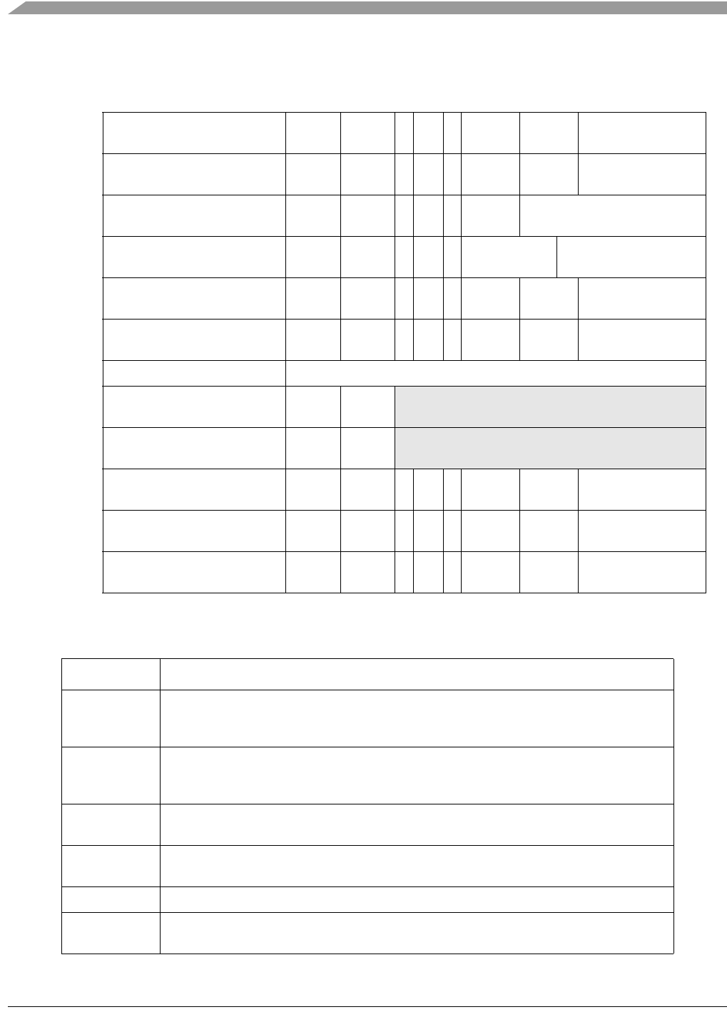
MCF548x Reference Manual, Rev. 3
6-26 Freescale Semiconductor
Table 6-24 defines the terminology used in Table 6-23.
FMOVE 1111001000 ea
mode
ea reg 0 r/m 0 src spec dest reg opmode
1111001000 ea
mode
ea reg 0 1 1 dest fmt src reg 0 0 0 0 0 0 0
1111001000 ea
mode
ea reg 1 0 d
r
reg sel 00 00000000
FMOVEM 1111001000 ea
mode
ea reg 1 1 d
r
10 0 00 register list
FMUL 1111001000 ea
mode
ea reg 0 r/m 0 src spec dest reg opmode
FNEG 1111001000 ea
mode
ea reg 0 r/m 0 src spec dest reg opmode
FNOP 11110010100000000 0 000 0 00 0 0000000
FRESTOR
E
1111001101 ea
mode
ea reg
FSAVE 1111001100 ea
mode
ea reg
FSQRT 1111001000 ea
mode
ea reg 0 r/m 0 src spec dest reg opmode
FSUB 1111001000 ea
mode
ea reg 0 r/m 0 src spec dest reg opmode
FTST 1111001000 ea
mode
ea reg 0 r/m 0 src spec dest reg 0 1 1 1 0 1 0
Table 6-24. Instruction Format Terminology
Term Definition
Instructions Instructions appear in memory as sequential, 16-bit values, and are read in the above table
left to right. An instruction can have from 1 to 3 16-bit words. A shaded block indicates this
word is never used and is not present.
EA MODE
EA REG
Defines the effective address for an operand located external to the FPU. For most FPU
instructions, this field defines the location of an external source operand; for FP store
operations, it specifies the destination location.
R/M If R/M = 0, an FPU data register is one source operand, otherwise the source operand is
specified by the EA {MODE, REG} fields.
SRC SPEC Defines the format (byte, word, longword, single-, or double-precision) of an external
operand.
DEST REG Specifies the destination FPU data register.
COND
PREDICATE
Defines the condition to be evaluated (EQ, NE, and so on) during the execution of the FPU
conditional branch instruction.
Table 6-23. Floating-Point Instruction Formats (Continued)
Mnemonic Instruction Code

Instructions
MCF548x Reference Manual, Rev. 3
Freescale Semiconductor 6-27
6.7.2 Floating-Point Instruction Execution Timing
Table 6-25 shows the ColdFire execution times for the floating-point instructions in terms of processor
core clock cycles. Each timing entry is presented as C(r/w).
• C = The number of processor clock cycles including all applicable operand reads and writes plus
all internal core cycles required to complete instruction execution
•r = The number of operand reads
•w = The number of operand writes
NOTE
Timing assumptions are the same as those for the ColdFire ISA. See the
ColdFire Microprocessor Family Programmer’s Reference Manual.
OPMODE Defines the exact operation to be performed by the FPU.
SZ Defines the length of the PC-relative displacement for the FPU conditional branch
instruction. If SZ = 0, the displacement is 16 bits, otherwise a 32-bit displacement is used.
dr Specifies direction of the MOVE transfer. As a 0, it moves from memory to the FP; as 1, it
moves from the FP to memory.
REGISTER
LIST
Defines FPU data registers to be moved during the execution of the FMOVEM instruction.
REG SEL Indicates the FPU control register to be moved during execution of an FMOVE control
register instruction.
Table 6-25. Floating-Point Instruction Execution Times1, 2, 3
Opcode Format
Effective Address <ea>
FPn Dn (An) (An)+ -(An) (d16,An) (d16,PC)
FABS <ea>y,FPx 1(0/0) 1(0/0) 1(1/0) 1(1/0) 1(1/0) 1(1/0) 1(1/0)
FADD <ea>y,FPx 4(0/0) 4(0/0) 4(1/0) 4(1/0) 4(1/0) 4(1/0) 4(1/0)
FBcc <label> — — — — — — 2(0/0) if correct,
9(0/0) if incorrect
FCMP <ea>y,FPx 4(0/0) 4(0/0) 4(1/0) 4(1/0) 4(1/0) 4(1/0) 4(1/0)
FDIV <ea>y,FPx 23(0/0) 23(0/0) 23(1/0) 23(1/0) 23(1/0) 23(1/0) 23(1/0)
FINT <ea>y,FPx 4(0/0) 4(0/0) 4(1/0) 4(1/0) 4(1/0) 4(1/0) 4(1/0)
FINTRZ <ea>y,FPx 4(0/0) 4(0/0) 4(1/0) 4(1/0) 4(1/0) 4(1/0) 4(1/0)
FMOVE <ea>y,FPx 1(0/0) 1(0/0) 1(1/0) 1(1/0) 1(1/0) 1(1/0) 1(1/0)
FPy,<ea>x — 2(0/1) 2(0/1) 2(0/1) 2(0/1) 2(0/1) —
<ea>y,FP*R — 6(0/0) 6(1/0) 6(1/0) 6(1/0) 6(1/0) 6(1/0)
FP*R,<ea>x — 1(0/0) 1(0/1) 1(0/1) 1(0/1) 1(0/1) —
Table 6-24. Instruction Format Terminology (Continued)
Term Definition

MCF548x Reference Manual, Rev. 3
6-28 Freescale Semiconductor
The ColdFire architecture supports concurrent execution of integer and floating-point instructions. The
latencies in this table define the execution time needed by the FPU. After a multi-cycle FPU instruction is
issued, subsequent integer instructions can execute concurrently with the FPU execution. For this
sequence, the floating-point instruction occupies only one OEP cycle.
6.7.3 Key Differences between ColdFire and M68000 FPU Programming
Models
This section is intended for compiler developers and developers porting assembly language routines from
the M68000 family to ColdFire. It highlights major differences between the ColdFire FPU instruction set
architecture (ISA) and the equivalent M68000 family ISA, using the MC68060 as the reference. The
internal FPU datapath width is the most obvious difference. ColdFire uses 64-bit double-precision and the
M68000 family uses 80-bit extended precision. Other differences pertain to supported addressing modes,
both across all FPU instructions as well as specific opcodes. Table 6-26 lists key differences. Because all
ColdFire implementations support instruction sizes of 48 bits or less, M68000 operations requiring larger
instruction lengths cannot be supported.
.
FMOVEM 4<ea>y,#list — — 2n(2n/0) — — 2n(2n/0) 2n(2n/0)
#list,<ea>x — — 1+2n(0/2n) — — 1+2n(0/2n) —
FMUL <ea>y,FPx 4(0/0) 4(0/0) 4(1/0) 4(1/0) 4(1/0) 4(1/0) 4(1/0)
FNEG <ea>y,FPx 1(0/0) 1(0/0) 1(1/0) 1(1/0) 1(1/0) 1(1/0) 1(1/0)
FNOP —————— 2(0/0)
FRESTORE <ea>y — — 6(4/0) — — 6(4/0) 6(4/0)
FSAVE <ea>x — — 7(0/4) — — 7(0/4) —
FSQRT <ea>y,FPx 56(0/0) 56(0/0) 56(1/0) 56(1/0) 56(1/0) 56(1/0) 56(1/0)
FSUB <ea>y,FPx 4(0/0) 4(0/0) 4(1/0) 4(1/0) 4(1/0) 4(1/0) 4(1/0)
FTST <ea>y,FPx 1(0/0) 1(0/0) 1(1/0) 1(1/0) 1(1/0) 1(1/0) 1(1/0)
1Add 1(1/0) for an external read operand of double-precision format for all instructions except FMOVEM, and 1(0/1)
for FMOVE FPy,<ea>x when the destination is double-precision.
2If the external operand is an integer format (byte, word, longword), there is a 4 cycle conversion time which must be
added to the basic execution time.
3If any exceptions are enabled, the execution time for FMOVE FPy,<ea>x increases by one cycle. If the BSUN
exception is enabled, the execution time for FBcc increases by one cycle.
4For FMOVEM, n refers to the number of registers being moved.
Table 6-26. Key Programming Model Differences
Feature M68000 ColdFire
Internal datapath width 80 bits 64 bits
Support for fpGEN d8(An,Xi),FPx Yes No
Table 6-25. Floating-Point Instruction Execution Times1, 2, 3 (Continued)
Opcode Format
Effective Address <ea>
FPn Dn (An) (An)+ -(An) (d16,An) (d16,PC)

Instructions
MCF548x Reference Manual, Rev. 3
Freescale Semiconductor 6-29
Some differences affect function activation and return. M68000 subroutines typically began with
FMOVEM #list,-(a7) to save registers on the system stack, with each register occupying three longwords.
In ColdFire, each register occupies two longwords and the stack pointer must be adjusted before the
FMOVEM instruction. A similar sequence generally occurs at the end of the function, preparing to return
control to the calling routine.
The examples in Table 6-27, Table 6-28, and Table 6-29 show a M68000 operation and the equivalent
ColdFire sequence.
If the subroutine includes LINK and UNLK instructions, the stack space needed for FPU register storage
can be factored into these operations and LEA instructions are not required.
The M68000 FPU supports loads and stores of multiple control registers (FPCR, FPSR, and FPIAR) with
one instruction. For ColdFire, only one can be moved at a time.
For instructions that require an unsupported addressing mode, the operand address can be formed with a
LEA instruction immediately before the FPU operation. See Table 6-28.
The M68000 FPU allows floating-point instructions to directly specify immediate values; the ColdFire
FPU does not support these types of immediate constants. It is recommended that floating-point immediate
Support for fpGEN xxx.{w,l},FPx Yes No
Support for fpGEN d8(PC,Xi),FPx Yes No
Support for fpGEN #xxx,FPx Yes No
Support for fmovem (Ay)+,#list Yes No
Support for fmovem #list,-(Ax) Yes No
Support for fmovem FP Control Registers Yes No
Table 6-27. M68000/ColdFire Operation Sequence 11
1 n is the number of FP registers to be saved/restored.
M68000 ColdFire Equivalent
fmovem.x #list,-(a7) lea -8*n(a7),a7;allocate stack space
fmovem.d #list,(a7) ;save FPU registers
fmovem.x (a7)+,#list fmovem.d (a7),#list ;restore FPU registers
lea 8*n(a7),a7 ;deallocate stack space
Table 6-28. M68000/ColdFire Operation Sequence 2
M68000 ColdFire Equivalent
fadd.s label,fp2 lea label,a0;form pointer to data
fadd.s (a0),fp2
fmul.d (d8,a1,d7),fp5 lea (d8,a1,d7),a0;form pointer to data
fmul.d (a0),fp5
fcmp.l (d8,pc,d2),fp3 lea (d8,pc,d2),a0;form pointer to data
fcmp.l (a0),fp3
Table 6-26. Key Programming Model Differences (Continued)
Feature M68000 ColdFire

MCF548x Reference Manual, Rev. 3
6-30 Freescale Semiconductor
values be moved into a table of constants that can be referenced using PC-relative addressing or as an offset
from another address pointer. See Table 6-29.
Finally, ColdFire and the M68000 differ in how exceptions are made pending. In the ColdFire exception
model, asserting both an FPSR exception indicator bit and the corresponding FPCR enable bit makes an
exception pending. Thus, a pending exception state can be created by loading FPSR and/or FPCR. On the
M68000, this type of pending exception is not possible.
Analysis of compiled floating-point applications indicates these differences account for most of the
changes between M68000-compatible text and the equivalent ColdFire program.
Table 6-29. M68000/ColdFire Operation Sequence 3
M68000 ColdFire Equivalent
fadd.l #imm1,fp3 fadd.l (imm1_label,pc),fp3
fsub.s #imm2,fp4 fsub.s (imm2_label,pc),fp3
fdiv.d #imm3,fp5 fdiv.d (imm3_label,pc),fp3
align 4
imm1_label:
long imm1 ;integer longword
imm2_label:
long imm2 ;single-precision
imm3_label:
long imm3_upper,
imm3_lower ;double-precision

MCF548x Reference Manual, Rev. 3
Freescale Semiconductor 7-1
Chapter 7
Local Memory
This chapter describes the MCF548x implementation of the ColdFire Version 4e local memory
specification. It consists of two major sections.
•Section 7.2, “SRAM Overview,” describes the MCF548x core’s local static RAM (SRAM)
implementation. It covers general operations, configuration, and initialization. It also provides
information and examples showing how to minimize power consumption when using the SRAM.
•Section 7.7, “Cache Overview,” describes the MCF548x cache implementation, including
organization, configuration, and coherency. It describes cache operations and how the cache
interfaces with other memory structures.
7.1 Interactions between Local Memory Modules
Depending on configuration information, instruction fetches and data read accesses may be sent
simultaneously to the SRAM and cache controllers. This approach is required because all three controllers
are memory-mapped devices, and the hit/miss determination is made concurrently with the read data
access. Power dissipation can be minimized by configuring the RAMBARs to mask unused address spaces
whenever possible.
If the access address is mapped into the region defined by the SRAM (and this region is not masked), the
SRAM provides the data back to the processor, and the cache data is discarded. Accesses from the SRAM
module are never cached. The complete definition of the processor’s local bus priority scheme for read
references is as follows:
if (SRAM “hits”)
SRAM supplies data to the processor
else if (data cache “hits”)
data cache supplies data to the processor
else system memory reference to access data
For data write references, the memory mapping into the local memories is resolved before the appropriate
destination memory is accessed. Accordingly, only the targeted local memory is accessed for data write
transfers.
NOTE
The two SRAMs discussed in this chapter is on the processor local bus.
There is a third 32-Kbyte SRAM on the MCF548x device. See Chapter 16,
“32-Kbyte System SRAM,” for more information.
7.2 SRAM Overview
The two 4-Kbyte, on-chip SRAM modules provide the core with pipelined, single-cycle access to memory.
Memory can be independently mapped to any 0-modulo-4K location in the 4-Gbyte address space and
configured to respond to either instruction or data accesses.
The following summarizes features of the MCF548x SRAM implementation:
• Two 4-Kbyte SRAMs, organized as 1024 x 32 bits
• Single-cycle throughput. When the pipeline is full, one access can occur per clock cycle.

MCF548x Reference Manual, Rev. 3
7-2 Freescale Semiconductor
• Physical location on the processor’s high-speed local bus with a user-programmed connection to
the internal instruction or data bus
• Memory location programmable on any 0-modulo-4K address boundary
• Byte, word, and longword address capabilities
• The RAM base address registers (RAMBAR0 and RAMBAR1) define the logical base address,
attributes, and access types for the two SRAM modules.
7.3 SRAM Operation
Each SRAM module provides a general-purpose memory block that the ColdFire processor can access
with single-cycle throughput. The location of the memory block can be specified to any 0-module-4K
address boundary in the 4-Gbyte address space by RAMBARn[BA], described in Section 7.4.1, “SRAM
Base Address Registers (RAMBAR0/RAMBAR1).” The memory is ideal for storing critical code or data
structures or for use as the system stack. Because the SRAM module connects physically to the processor’s
high-speed local bus, it can service processor-initiated accesses or memory-referencing debug module
commands.
The Version 4e ColdFire processor core implements a Harvard memory architecture. Each SRAM module
may be logically connected to either the processor’s internal instruction or data bus. This logical
connection is controlled by a configuration bit in the RAM base address registers (RAMBAR0 and
RAMBAR1).
If an instruction fetch is mapped into the region defined by the SRAM, the SRAM sources the data to the
processor and any cache data is discarded. Likewise, if a data access is mapped into the region defined by
the SRAM, the SRAM services the access and the cache is not affected. Accesses from SRAM modules
are never cached, and debug-initiated references are treated as data accesses.
Note also that the SRAMs cannot be accessed by the on-chip DMAs. The on-chip system configuration
allows concurrent core and DMA execution, where the CPU can reference code or data from the internal
SRAMs or caches while performing a DMA transfer.
Accesses are attempted in the following order:
1. SRAM
2. Cache (if space is defined as cacheable)
3. System SRAM, MBAR space, or external access
7.4 SRAM Register Definition
The SRAM programming model consists of RAMBAR0 and RAMBAR1.
7.4.1 SRAM Base Address Registers (RAMBAR0/RAMBAR1)
The SRAM modules are configured through the RAMBARs, shown in Figure 7-1. Each RAMBAR holds
the base address of the SRAM. The MOVEC instruction provides write-only access to this register from
the processor. Each RAMBAR can be read or written from the debug module in a similar manner. All
undefined RAMBAR bits are reserved. These bits are ignored during writes to the RAMBAR and return
zeros when read from the debug module. The valid bits, RAMBARn[V], are cleared at reset, disabling the
SRAM modules. All other bits are unaffected.
NOTE
RAMBARn is read/write by the debug module.

SRAM Register Definition
MCF548x Reference Manual, Rev. 3
Freescale Semiconductor 7-3
RAMBARn fields are described in detail in Table 7-1.
31 30 29 28 27 26 25 24 23 22 21 20 19 18 17 16
RBA
W
Reset00000 0000 0000000
15 14 13 12 11 10 9 8 7 6 5 4 3 2 1 0
R BA 0 0 0 WP D/I 0 C/I SC SD UC UD V
W
Reset00000 0000 0000000
Reg
Addr
CPU space + 0xC04 (RAMBAR0), 0xC05 (RAMBAR1)
Figure 7-1. SRAM Base Address Registers (RAMBARn)
Table 7-1. RAMBARn Field Description
Bits Name Description
31–12 BA Base address. Defines the SRAM module’s word-aligned base address. Each SRAM
module occupies a 4-Kbyte space defined by the contents of BA. SRAM may reside on any
4-Kbyte boundary in the 4 Gbyte address space.
11–9 — Reserved. Should be cleared.
8 WP Write protect. Controls read/write properties of the SRAM.
0 Allows read and write accesses to the SRAM module
1 Allows only read accesses to the SRAM module. Any attempted write reference
generates an access error exception to the ColdFire processor core.
7 D/I Data/instruction bus. Indicates whether SRAM is connected to the internal data or
instruction bus.
0 Data bus
1 Instruction bus
6 — Reserved, should be cleared.

MCF548x Reference Manual, Rev. 3
7-4 Freescale Semiconductor
The mapping of a given access into the SRAM uses the following algorithm to determine if the access hits
in the memory:
if (RAMBAR[0] = 1)
if (((access = instructionFetch) & (RAMBAR[7] = 1)) |
((access = dataReference) & (RAMBAR[7] = 0)))
if (requested address[31:10] = RAMBAR[31:10])
if (requested address[31:n] = RAMBAR[31:n]
if (ASn of the requested type = 0)
Access is mapped to the SRAM module
if (access = read)
Read the SRAM and return the data
if (access = write)
if (RAMBAR[8] = 0)
Write the data into the SRAM
else Signal a write-protect access error
ASn refers to the five address space mask bits: C/I, SC, SD, UC, and UD.
7.5 SRAM Initialization
After a hardware reset, the contents of each SRAM module are undefined. The valid bits, RAMBARn[V],
are cleared, disabling the SRAM modules. If the SRAM requires initialization with instructions or data,
the following steps should be performed:
1. Load RAMBARn with bit 7 = 0, mapping the SRAM module to the desired location. Clearing
RAMBARn[7] logically connects the SRAM module to the processor’s data bus.
2. Read the source data and write it to the SRAM. Various instructions support this function,
including memory-to-memory move instructions and the move multiple instruction (MOVEM).
MOVEM is optimized to generate line-sized burst fetches on line-aligned addresses, so it
generally provides maximum performance.
5 C/I Address space masks (ASn). These fields allow certain types of accesses to be masked,
or inhibited from accessing the SRAM module. These bits are useful for power
management as described in Section 7.6, “Power Management.” In particular, C/I is
typically set.
The address space mask bits are follows:
C/I = CPU space/interrupt acknowledge cycle mask. Note that C/I must be set if BA = 0.
SC = Supervisor code address space mask
SD = Supervisor data address space mask
UC = User code address space mask
UD = User data address space mask
For each ASn bit:
0 An access to the SRAM module can occur for this address space
1 Disable this address space from the SRAM module. If a reference using this address
space is made, it is inhibited from accessing the SRAM module and is processed like
any other non-SRAM reference.
4SC
3SD
2UC
1UD
0 V Valid. Enables/disables the SRAM module. V is cleared at reset.
0 RAMBAR contents are not valid.
1 RAMBAR contents are valid.
Table 7-1. RAMBARn Field Description (Continued)
Bits Name Description

SRAM Initialization
MCF548x Reference Manual, Rev. 3
Freescale Semiconductor 7-5
3. After the data is loaded into the SRAM, it may be appropriate to revise the RAMBAR attribute
bits, including the write-protect and address-space mask fields. If the SRAM contains
instructions, RAMBAR[D/I] must be set to logically connect the memory to the processor’s
internal instruction bus.
Remember that the SRAM cannot be accessed by the on-chip DMAs. The on-chip system configuration
allows concurrent core and DMA execution, where the core can execute code out of internal SRAM or
cache during DMA access.
The ColdFire processor or an external emulator using the debug module can perform these initialization
functions.
7.5.1 SRAM Initialization Code
The code segment below initializes the SRAM using RAMBAR0. The code sets the base address of the
SRAM at 0x2000_0000 before it initializes the SRAM to zeros.
RAMBASE EQU 0x20000000 ;set this variable to 0x20000000
RAMVALID EQU 0x00000035
move.l #RAMBASE+RAMVALID,D0 ;load RAMBASE + valid bit into D0
movec.l D0, RAMBAR0;load RAMBAR0 and enable SRAM
The following loop initializes the entire SRAM to zero:
lea.l RAMBASE,A0 ;load pointer to SRAM
move.l #1024,D0 ;load loop counter into D0
SRAM_INIT_LOOP:
clr.l (A0)+ ;clear 4 bytes of SRAM
subq.l #1,D0 ;decrement loop counter
bne.b SRAM_INIT_LOOP ;exit if done; else continue looping
The following function copies the number of bytesToMove from the source (*src) to the processor’s local
SRAM at an offset relative to the SRAM base address defined by destinationOffset. The bytesToMove
must be a multiple of 16. For best performance, source and destination SRAM addresses should be
line-aligned (0-modulo-16).
; copyToCpuRam (*src, destinationOffset, bytesToMove)
RAMBASE EQU 0x20000000 ;SRAM base address
RAMFLAGS EQU 0x00000035 ;RAMBAR valid + mask bits
lea.l -12(a7),a7;allocate temporary space
movem.l #0x1c,(a7);store D2/D3/D4 registers
; stack arguments and locations
; +0 saved d2
; +4 saved d3
; +8 saved d4
; +12 returnPc
; +16 pointer to source operand

MCF548x Reference Manual, Rev. 3
7-6 Freescale Semiconductor
; +20 destinationOffset
; +24 bytesToMove
move.l RAMBASE+RAMFLAGS,a0 ;define RAMBAR0 contents
movec.l a0,rambar0;load it
move.l 16(a7),a0;load argument defining *src
lea.l RAMBASE,a1;memory pointer to SRAM base
add.l 20(a7),a1;include destinationOffset
move.l 24(a7),d4;load byte count
asr.l #4,d4 ;divide by 16 to convert to loop count
.align 4 ;force loop on 0-mod-4 address
loop: movem.l (a0),#0xf;read 16 bytes from source
movem.l #0xf,(a1);store into SRAM destination
lea.l 16(a0),a0;increment source pointer
lea.l 16(a1),a1;increment destination pointer
subq.l #1,d4 ;decrement loop counter
bne.b loop ;if done, then exit, else continue
movem.l (a7),#0x1c;restore d2/d3/d4 registers
lea.l 12(a7),a7;deallocate temporary space
rts
7.6 Power Management
Because processor memory references may be simultaneously sent to an SRAM module and cache, power
can be minimized by configuring RAMBAR address space masks as precisely as possible. For example,
if an SRAM is mapped to the internal instruction bus and contains instruction data, setting the ASn mask
bits associated with operand references can decrease power dissipation. Similarly, if the SRAM contains
data, setting ASn bits associated with instruction fetches minimizes power.
Table 7-2 shows typical RAMBAR configurations.
.
7.7 Cache Overview
This section describes the MCF548x cache implementation, including organization, configuration, and
coherency. It describes cache operations and how the cache interacts with other memory structures.
The MCF548x implements a special branch instruction cache for accelerating branches, enabled by a bit
in the cache access control register (CACR[BEC]). The branch cache is described in Section 3.2.1.1.1,
“Branch Acceleration.”
Table 7-2. Examples of Typical RAMBAR Settings
Data Contained in SRAM RAMBAR[5–0]
Code only 0x2B
Data only 0x35
Both code and data 0x21
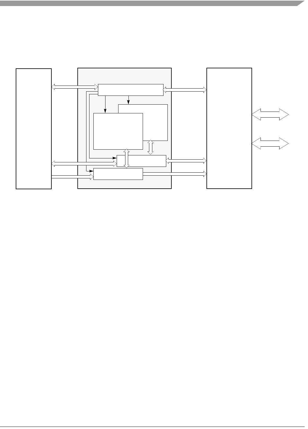
Cache Organization
MCF548x Reference Manual, Rev. 3
Freescale Semiconductor 7-7
The MCF548x processor’s Harvard memory structure includes a 32-Kbyte data cache and a 32-Kbyte
instruction cache. Both are nonblocking and 4-way set-associative with a 16-byte line. The cache improves
system performance by providing single-cycle access to the instruction and data pipelines. This decouples
processor performance from system memory performance, increasing bus availability for on-chip DMA
or external devices. Figure 7-2 shows the organization and integration of the data cache.
Figure 7-2. Data Cache Organization
Both caches implement line-fill buffers to optimize line-sized burst accesses. The data cache supports
operation of copyback, write-through, or cache-inhibited modes. A four-entry, 32-bit buffer supports cache
line-push operations, and can be configured to defer write buffering in write-through or cache-inhibited
modes. The cache lock feature can be used to guarantee deterministic response for critical code or data
areas.
A nonblocking cache services read hits or write hits from the processor while a fill (caused by a cache
allocation) is in progress. As Figure 7-2 shows, accesses use a single bus connected to the cache.
All addresses from the processor to the cache are physical addresses. A cache hit occurs when an address
matches a cache entry. For a read, the cache supplies data to the processor. For a write, which is permitted
only to the data cache, the processor updates the cache. If an access does not match a cache entry (misses
the cache) or if a write access must be written through to memory, the cache performs a bus cycle on the
internal bus and correspondingly on the external bus by way of the system integration unit (SIU).
The cache module does not implement bus snooping; cache coherency with other possible bus masters
must be maintained in software.
7.8 Cache Organization
A four-way set associative cache is organized as four ways (levels). There are 512 sets in the 32-Kbyte
data cache with each line containing 16 bytes (4 longwords). The 32-Kbyte instruction cache has 512 sets.
Entire cache lines are loaded from memory by burst-mode accesses that cache 4 longwords of data or
instructions. All 4 longwords must be loaded for the cache line to be valid.
Figure 7-3 shows data cache organization as well as terminology used.
System
Address/
Control
Cache
Control Logic
Directory Array
Data Array
Data Path
ColdFire
Address Path
Control
Data
Address
External
Bus
Data
Control
Data
Address
Integration
Unit
(SIU)
Processor
Core

MCF548x Reference Manual, Rev. 3
7-8 Freescale Semiconductor
Figure 7-3. Data Cache Organization and Line Format
A set is a group of four lines (one from each level, or way), corresponding to the same index into the cache
array.
7.8.1 Cache Line States: Invalid, Valid-Unmodified, and Valid-Modified
As shown in Table 7-3, a data cache line can be invalid, valid-unmodified (often called exclusive), or
valid-modified. An instruction cache line can be valid or invalid.
A valid line can be explicitly invalidated by executing a CPUSHL instruction.
7.8.2 The Cache at Start-Up
As Figure 7-4 (A) shows, after power-up, cache contents are undefined; V and M may be set on some lines
even though the cache may not contain the appropriate data for start up. Because reset and power-up do
not invalidate cache lines automatically, the cache should be cleared explicitly by setting
CACR[DCINVA,ICINVA] before the cache is enabled (B).
After the entire cache is flushed, cacheable entries are loaded first in way 0. If way 0 is occupied, the
cacheable entry is loaded into the same set in way 1, as shown in Figure 7-4 (D). This process is described
in detail in Section 7.9, “Cache Operation.”
Table 7-3. Valid and Modified Bit Settings
VM Description
0 x Invalid. Invalid lines are ignored during lookups.
1 0 Valid, unmodified. Cache line has valid data that matches system memory.
1 1 Valid, modified. Cache line contains most recent data, data at system memory location is
stale.
Way 0 Way 1 Way 2 Way 3
Line
Set 0
Set 1
Set 510
Set 511
•
•
•
•
•
•
•
•
•
•
•
•
TAG V M Longword 0 Longword 1 Longword 2 Longword 3
Where:
TAG—21-bit address tag
V—Valid bit for line
M—Modified bit for line (data cache only)
Cache Line Format
Cache Organization
MCF548x Reference Manual, Rev. 3
Freescale Semiconductor 7-9
Figure 7-4. Data Cache—A: at Reset, B: after Invalidation, C and D: Loading Pattern
A: Cache population at
start-up
B: Cache after invalidation,
before it is enabled
C: Cache after loads in
Way 0
D: First load in Way 1
Way 0Way 1Way 2Way 3 Way 0Way 1Way 2Way 3 Way 0Way 1Way 2Way 3 Way 0Way 1Way 2Way
3
Invalid (V = 0)
Valid, not modified (V = 1, M = 0)
Valid, modified (V = 1, M = 1)
At reset, cache contents
are indeterminate; V and
M may be set. The cache
should be cleared
explicitly by setting
CACR[DCINVA] before
the cache is enabled.
Setting CACR[DCINVA]
invalidates the entire
cache.
Set 0
Set 511
Initial cacheable
accesses to memory-fill
positions in way 0.
A line is loaded in way 1
only if that set is full in
way 0.
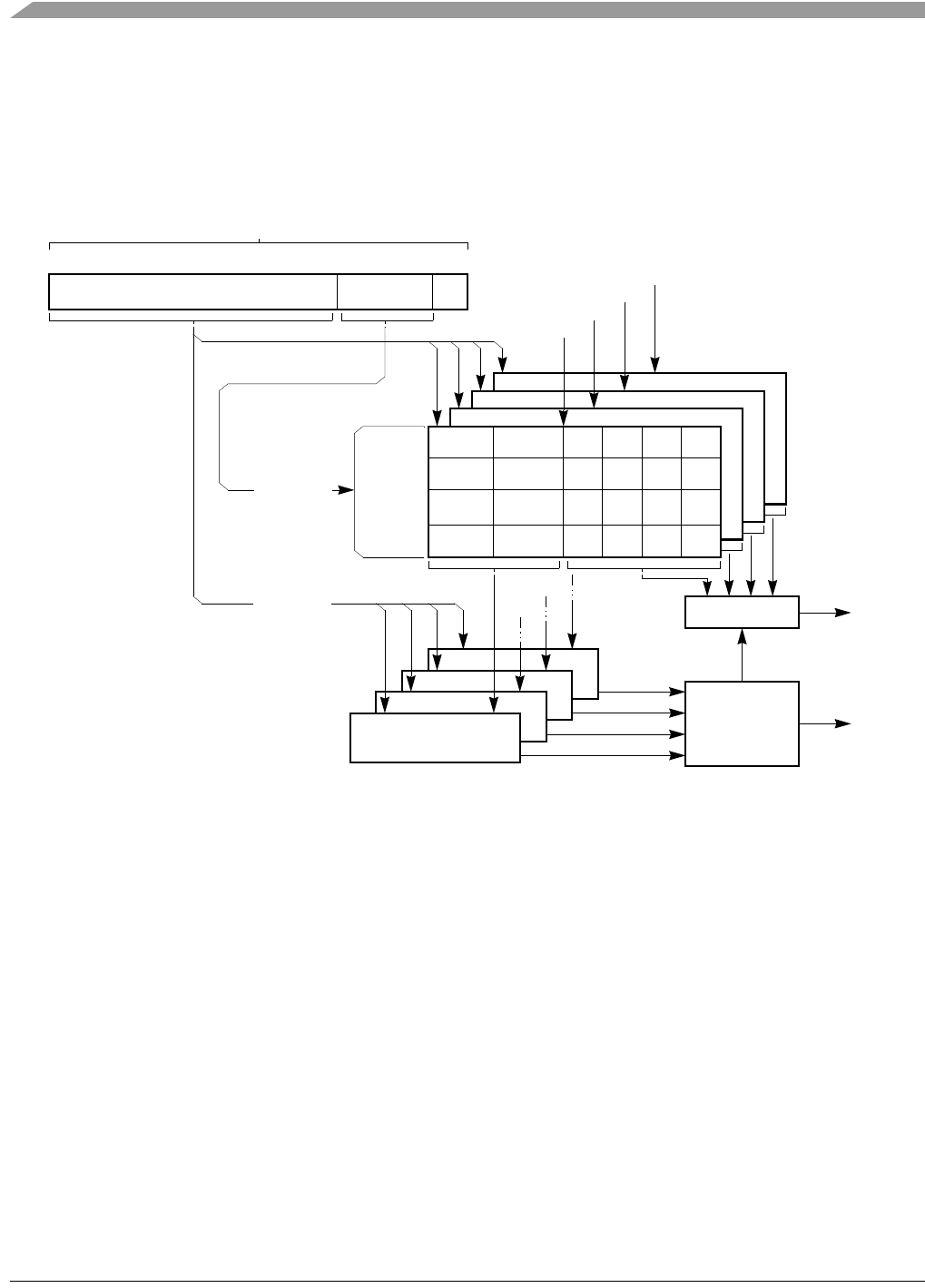
MCF548x Reference Manual, Rev. 3
7-10 Freescale Semiconductor
7.9 Cache Operation
Figure 7-5 shows the general flow of a caching operation using the 32-Kbyte data cache as an example.
The discussion in this chapter assumes a data cache. Instruction cache operations are similar except that
there is no support for writing to the cache; therefore, such notions of modified cache lines and write
allocation do not apply.
Figure 7-5. Data Caching Operation
The following steps determine if a data cache line is allocated for a given address:
1. The cache set index, A[12:4], selects one cache set.
2. A[31:13] and the cache set index are used as a tag reference or are used to update the cache line
tag field. Note that A[31:13] can specify 19 possible address lines that can be mapped to one of
the four ways.
3. The four tags from the selected cache set are compared with the tag reference. A cache hit occurs
if a tag matches the tag reference and the V bit is set, indicating that the cache line contains valid
data. If a cacheable write access hits in a valid cache line, the write can occur to the cache line
without having to load it from memory.
If the memory space is copyback, the updated cache line is marked modified (M = 1), because the
new data has made the data in memory out of date. If the memory location is write-through, the
write is passed on to system memory and the M bit is never used. Note that the tag does not have
TT or TM bits.
To allocate a cache entry, the cache set index selects one of the cache’s 512 sets. The cache control logic
looks for an invalid cache line to use for the new entry. If none is available, the cache controller uses a
034121331
Index
Tag Data/Tag Reference
MUX
Comparator 0
1
2
3
Logical OR
Hit 3
Hit 2
Hit 1
Hit 0
Hit
Line Select
Set 0
Set 1
Set 511
•
•
•
Address
A[31:13]
Way 0
Way 1
Way 2
Way 3
TAG STATUSLW0LW1LW2LW3
TAG STATUS LW0 LW1 LW2 LW3
•
•
••
•
••
•
••
•
••
•
••
•
•
Address
Set
Select
A[12:4]
Data

Cache Operation
MCF548x Reference Manual, Rev. 3
Freescale Semiconductor 7-11
pseudo-round-robin replacement algorithm to choose the line to be deallocated and replaced. First the
cache controller looks for an invalid line, with way 0 the highest priority. If all lines have valid data, a 2-bit
replacement counter is used to choose the way. After a line is allocated, the pointer increments to point to
the next way.
Cache lines from ways 0 and 1 can be protected from deallocation by enabling half-cache locking. If
CACR[DHLCK,IHLCK] = 1, the replacement pointer is restricted to way 2 or 3.
As part of deallocation, a valid, unmodified cache line is invalidated. It is consistent with system memory,
so memory does not need to be updated. To deallocate a modified cache line, data is placed in a push buffer
(for an external cache line push) before being invalidated. After invalidation, the new entry can replace it.
The old cache line may be written after the new line is read.
When a cache line is selected to host a new cache entry, the following three things happen:
1. The new address tag bits A[31:13] are written to the tag.
2. The cache line is updated with the new memory data.
3. The cache line status changes to a valid state (V = 1).
Read cycles that miss in the cache allocate normally as previously described.
Write cycles that miss in the cache do not allocate on a cacheable write-through region, but do allocate for
addresses in a cacheable copyback region.
A copyback byte, word, longword, or line write miss causes the following:
1. The cache initiates a line fill or flush.
2. Space is allocated for a new line.
3. V and M are both set to indicate valid and modified.
4. Data is written in the allocated space. No write to memory occurs.
Note the following:
• Read hits cannot change the status bits and no deallocation or replacement occurs; the data or
instructions are read from the cache.
• If the cache hits on a write access, data is written to the appropriate portion of the accessed cache
line. Write hits in cacheable, write-through regions generate an external write cycle and the cache
line is marked valid, but is never marked modified. Write hits in cacheable copyback regions do
not perform an external write cycle; the cache line is marked valid and modified (V = 1 and M = 1).
• Misaligned accesses are broken into at least two cache accesses.
• Validity is provided only on a line basis. Unless a whole line is loaded on a cache miss, the cache
controller does not validate data in the cache line.
Write accesses designated as cache-inhibited by the CACR or ACR bypass the cache and perform a
corresponding external write.
Normally, cache-inhibited reads bypass the cache and are performed on the external bus. The exception to
this normal operation occurs when all of the following conditions are true during a cache-inhibited read:
• The cache-inhibited fill buffer bit, CACR[DNFB], is set.
• The access is an instruction read.
• The access is normal (that is, transfer type (TT) equals 0).
In this case, an entire line is fetched and stored in the fill buffer. It remains valid there, and the cache can
service additional read accesses from this buffer until either another fill or a cache-invalidate-all operation
occurs.

MCF548x Reference Manual, Rev. 3
7-12 Freescale Semiconductor
Valid cache entries that match during cache-inhibited address accesses are neither pushed nor invalidated.
Such a scenario suggests that the associated cache mode for this address space was changed. To avoid this,
it is generally recommended to use the CPUSHL instruction to push or invalidate the cache entry or set
CACR[DCINVA] to invalidate the data cache before switching cache modes.
7.9.1 Caching Modes
For every memory reference generated by the processor or debug module, a set of effective attributes is
determined based on the address and the ACRs. Caching modes determine how the cache handles an
access. A data access can be cacheable in either write-through or copyback mode; it can be cache-inhibited
in precise or imprecise modes. For normal accesses, the ACRn[CM] bit corresponding to the address of
the access specifies the caching modes. If an address does not match an ACR, the default caching mode is
defined by CACR[DDCM,IDCM]. The specific algorithm is as follows:
if (address == ACR0-address including mask)
effective attributes = ACR0 attributes
else if (address == ACR1-address including mask)
effective attributes = ACR1 attributes
else effective attributes = CACR default attributes
Addresses matching an ACR can also be write-protected using ACR[W]. Addresses that do not match
either ACR can be write-protected using CACR[DW].
Reset disables the cache and clears all CACR bits. As shown in Figure 7-4, reset does not automatically
invalidate cache entries; they must be invalidated through software.
The ACRs allow the defaults selected in the CACR to be overridden. In addition, some instructions (for
example, CPUSHL) and processor core operations perform accesses that have an implicit caching mode
associated with them. The following sections discuss the different caching accesses and their associated
cache modes.
7.9.1.1 Cacheable Accesses
If ACRn[CM] or the default field of the CACR indicates write-through or copyback, the access is
cacheable. A read access to a write-through or copyback region is read from the cache if matching data is
found. Otherwise, the data is read from memory and the cache is updated. When a line is being read from
memory for either a write-through or copyback read miss, the longword within the line that contains the
core-requested data is loaded first and the requested data is given immediately to the processor, without
waiting for the three remaining longwords to reach the cache.
The following sections describe write-through and copyback modes in detail. Note that some of this
information applies to data caches only.
7.9.1.1.1 Write-Through Mode (Data Cache Only)
Write accesses to regions specified as write-through are always passed on to the external bus, although the
cycle can be buffered, depending on the state of CACR[DESB]. Writes in write-through mode are handled
with a no-write-allocate policy—that is, writes that miss in the cache are written to the external bus but do
not cause the corresponding line in memory to be loaded into the cache. Write accesses that hit always
write through to memory and update matching cache lines. The cache supplies data to data-read accesses
that hit in the cache; read misses cause a new cache line to be loaded into the cache.

Cache Operation
MCF548x Reference Manual, Rev. 3
Freescale Semiconductor 7-13
7.9.1.1.2 Copyback Mode (Data Cache Only)
Copyback regions are typically used for local data structures or stacks to minimize external bus use and
reduce write-access latency. Write accesses to regions specified as copyback that hit in the cache update
the cache line and set the corresponding M bit without an external bus access.
The cache should be flushed using the CPUSHL instruction before invalidating the cache in copyback
mode using the CINV bit. Modified cache data is written to memory only if the line is replaced because of
a miss or a CPUSHL instruction pushes the line. If a byte, word, longword, or line write access misses in
the cache, the required cache line is read from memory, thereby updating the cache. When a miss selects
a modified cache line for replacement, the modified cache data moves to the push buffer. The replacement
line is read into the cache and the push buffer contents are then written to memory.
7.9.1.2 Cache-Inhibited Accesses
Memory regions can be designated as cache-inhibited, which is useful for memory containing targets such
as I/O devices and shared data structures in multiprocessing systems. It is also important to not cache the
MCF548x memory-mapped registers. If the corresponding ACRn[CM] or CACR[DDCM] indicates
cache-inhibited, precise or imprecise, the access is cache-inhibited. The caching operation is identical for
both cache-inhibited modes, which differ only regarding recovery from an external bus error.
In determining whether a memory location is cacheable or cache-inhibited, the CPU checks
memory-control registers in the following order:
1. RAMBARs
2. ACR0 and ACR2
3. ACR1 and ACR3
4. If an access does not hit in the RAMBARs or the ACRs, the default is provided for all accesses in
CACR.
Cache-inhibited write accesses bypass the cache, and a corresponding external write is performed.
Cache-inhibited reads bypass the cache and are performed on the external bus, except when all of the
following conditions are true:
• The cache-inhibited fill-buffer bit, CACR[DNFB], is set.
• The access is an instruction read.
• The access is normal (that is, TT = 0).
In this case, a fetched line is stored in the fill buffer and remains valid there; the cache can service
additional read accesses from this buffer until another fill occurs or a cache-invalidate-all operation occurs.
If ACRn[CM] indicates cache-inhibited mode, precise or imprecise, the controller bypasses the cache and
performs an external transfer. If a line in the cache matches the address and the mode is cache-inhibited,
the cache does not automatically push the line if it is modified, nor does it invalidate the line if it is valid.
Before switching cache mode, execute a CPUSHL instruction or set CACR[DCINVA,ICINVA] to
invalidate the entire cache.
If ACRn[CM] indicates precise mode, the sequence of read and write accesses to the region is guaranteed
to match the instruction sequence. In imprecise mode, the processor core allows read accesses that hit in
the cache to occur before completion of a pending write from a previous instruction. Writes are not
deferred past data-read accesses that miss the cache (that is, that must be read from the bus).
Precise operation forces data-read accesses for an instruction to occur only once by preventing the
instruction from being interrupted after data is fetched. Otherwise, if the processor is not in precise mode,
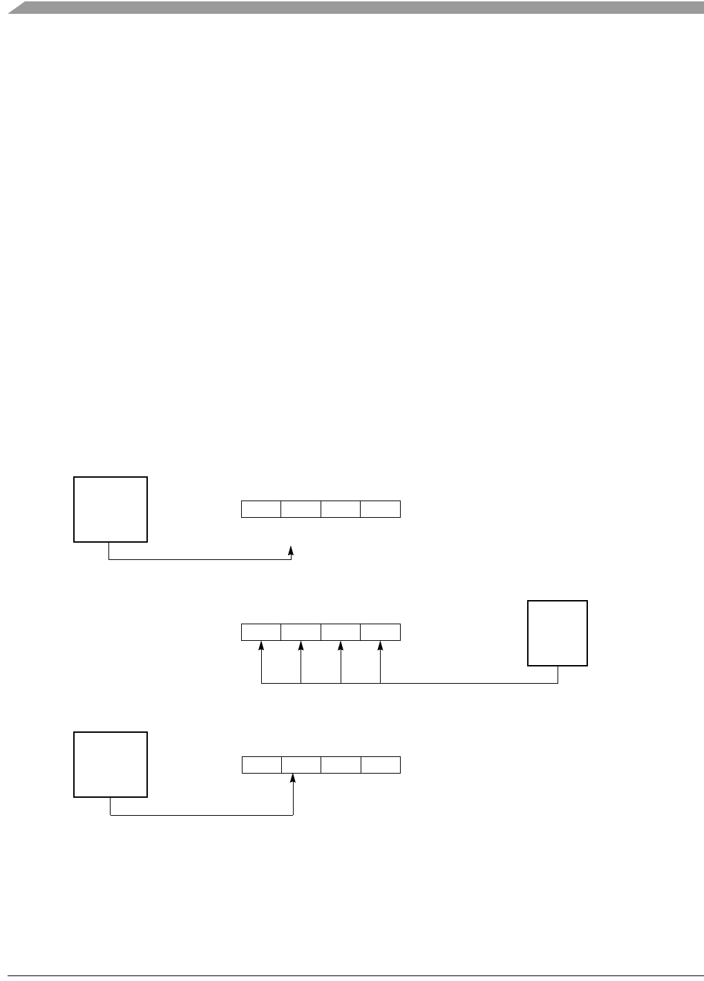
MCF548x Reference Manual, Rev. 3
7-14 Freescale Semiconductor
an exception aborts the instruction and the data may be accessed again when the instruction is restarted.
These guarantees apply only when ACRn[CM] indicates precise mode and aligned accesses.
CPU space-register accesses using the MOVEC instruction are treated as cache-inhibited and precise.
7.9.2 Cache Protocol
The following sections describe the cache protocol for processor accesses and assumes that the data is
cacheable (that is, write-through or copyback). Note that the discussion of write operations applies to the
data cache only.
7.9.2.1 Read Miss
A processor read that misses in the cache requests the cache controller to generate a bus transaction. This
bus transaction reads the needed line from memory and supplies the required data to the processor core.
The line is placed in the cache in the valid state.
7.9.2.2 Write Miss (Data Cache Only)
The cache controller handles processor writes that miss in the data cache differently for write-through and
copyback regions. Write misses to copyback regions cause the cache line to be read from system memory,
as shown in Figure 7-6.
Figure 7-6. Write-Miss in Copyback Mode
The new cache line is then updated with write data and the M bit is set for the line, leaving it in modified
state. Write misses to write-through regions write directly to memory without loading the corresponding
cache line into the cache.
Cache Line
System
V = 1
M = 0
1
. Writing character X to 0x0B generates a write miss. Data cannot be written to an invalid line.
Memory
V = 0
M = 0
0x0C 0x000x08 0x04
2
. The cache line (characters A–P) is updated from system memory, and the line is marked valid.
X
ABCD EFGH IJKL MNOP
3. After the cache line is filled, the write that initiated the write miss (the character X) completes to 0x0B.
V = 1
M = 1
0x0C 0x000x08 0x04
0x0C 0x000x08 0x04
ABCD EXGH IJKL MNOP
MCF548x
MCF548x

Cache Operation
MCF548x Reference Manual, Rev. 3
Freescale Semiconductor 7-15
7.9.2.3 Read Hit
On a read hit, the cache provides the data to the processor core and the cache line state remains unchanged.
If the cache mode changes for a specific region of address space, lines in the cache corresponding to that
region that contain modified data are not pushed out to memory when a read hit occurs within that line.
First execute a CPUSHL instruction or set CACR[DCINVA,ICINVA] before switching the cache mode.
7.9.2.4 Write Hit (Data Cache Only)
The cache controller handles processor writes that hit in the data cache differently for write-through and
copyback regions. For write hits to a write-through region, portions of cache lines corresponding to the
size of the access are updated with the data. The data is also written to external memory. The cache line
state is unchanged. For copyback accesses, the cache controller updates the cache line and sets the M bit
for the line. An external write is not performed and the cache line state changes to (or remains in) the
modified state.
7.9.3 Cache Coherency (Data Cache Only)
The MCF548x provides limited cache coherency support in multiple-master environments. Both
write-through and copyback memory update techniques are supported to maintain coherency between the
cache and memory.
The cache does not support snooping (that is, cache coherency is not supported while external or DMA
masters are using the bus). Therefore, on-chip DMAs of the MCF548x cannot access local memory and
do not maintain coherency with the data cache.
7.9.4 Memory Accesses for Cache Maintenance
The cache controller performs all maintenance activities that supply data from the cache to the core,
including requests to the SIU for reading new cache lines and writing modified lines to memory. The
following sections describe memory accesses resulting from cache fill and push operations. Chapter 17,
“FlexBus,” describes required bus cycles in detail.
7.9.4.1 Cache Filling
When a new cache line is required, a line read is requested from the SIU, which generates a burst-read
transfer by indicating a line access with the size signals, SIZ[1:0].
The responding device supplies 4 consecutive longwords of data. Burst operations can be inhibited or
enabled through the burst read/write enable bits (BSTR/BSTW) in the chip-select control registers
(CSCR0–CSCR7).
SIU line accesses implicitly request burst-mode operations from memory. For more information regarding
external bus burst-mode accesses, see Chapter 17, “FlexBus.”
The first cycle of a cache-line read loads the longword entry corresponding to the requested address.
Subsequent transfers load the remaining longword entries.
A burst operation is aborted by an a write-protection fault, which is the only possible access error.
Exception processing proceeds immediately. Note that unlike Version 2 and Version 3 access errors, the
program counter stored on the exception stack frame points to the faulting instruction. See Section 3.8.2,
“Processor Exceptions.”

MCF548x Reference Manual, Rev. 3
7-16 Freescale Semiconductor
7.9.4.2 Cache Pushes
Cache pushes occur for line replacement and as required for the execution of the CPUSHL instruction. To
reduce the requested data’s latency in the new line, the modified line being replaced is temporarily placed
in the push buffer while the new line is fetched from memory. After the bus transfer for the new line
completes, the modified cache line is written back to memory and the push buffer is invalidated.
7.9.4.2.1 Push and Store Buffers
The 16-byte push buffer reduces latency for requested new data on a cache miss by holding a displaced
modified data cache line while the new data is read from memory.
If a cache miss displaces a modified line, a miss read reference is immediately generated. While waiting
for the response, the current contents of the cache location load into the push buffer. When the burst-read
bus transaction completes, the cache controller can generate the appropriate line-write bus transaction to
write the push buffer contents into memory.
In imprecise mode, the FIFO store buffer can defer pending writes to maximize performance. The store
buffer can support as many as four entries (16 bytes maximum) for this purpose.
Data writes destined for the store buffer cannot stall the core. The store buffer effectively provides a
measure of decoupling between the pipeline’s ability to generate writes (one per cycle maximum) and the
external bus’s ability to retire those writes. In imprecise mode, writes stall only if the store buffer is full
and a write operation is on the internal bus. The internal write cycle is held, stalling the data execution
pipeline.
If the store buffer is not used (that is, store buffer disabled or cache-inhibited precise mode), external bus
cycles are generated directly for each pipeline write operation. The instruction is held in the pipeline until
external bus transfer termination is received. Therefore, each write is stalled for 5 cycles, making the
minimum write time equal to 6 cycles when the store buffer is not used. See Section 3.2.1.2, “Operand
Execution Pipeline (OEP).”
The data store buffer enable bit, CACR[DESB], controls the enabling of the data store buffer. This bit can
be set and cleared by the MOVEC instruction. DESB is zero at reset and all writes are performed in order
(precise mode). ACRn[CM] or CACR[DDCM] generates the mode used when DESB is set. Cacheable
write-through and cache-inhibited imprecise modes use the store buffer.
The store buffer can queue data as much as 4 bytes wide per entry. Each entry matches the corresponding
bus cycle it generates; therefore, a misaligned longword write to a write-through region creates two entries
if the address is to an odd-word boundary. It creates three entries if it is to an odd-byte boundary—one per
bus cycle.
7.9.4.2.2 Push and Store Buffer Bus Operation
As soon as the push or store buffer has valid data, the internal bus controller uses the next available external
bus cycle to generate the appropriate write cycles. In the event that another cache fill is required (for
example, cache miss to process) during the continued instruction execution by the processor pipeline, the
pipeline stalls until the push and store buffers are empty, then generate the required external bus
transaction.
Supervisor instructions, the NOP instruction, and exception processing synchronize the processor core and
guarantee the push and store buffers are empty before proceeding. Note that the NOP instruction should
be used only to synchronize the pipeline. The preferred no-operation function is the TPF instruction. See
the ColdFire Programmer’s Reference Manual for more information on the TPF instruction.

Cache Operation
MCF548x Reference Manual, Rev. 3
Freescale Semiconductor 7-17
7.9.5 Cache Locking
Ways 0 and 1 of the data cache can be locked by setting CACR[DHLCK]; likewise, ways 0 and 1 of the
instruction cache can be locked by setting CACR[IHLCK]. If a cache is locked, cache lines in ways 0 and
1 are not subject to being deallocated by normal cache operations.
As Figure 7-7 (B and C) shows, the algorithm for updating the cache and for identifying cache lines to be
deallocated is otherwise unchanged. If ways 2 and 3 are entirely invalid, cacheable accesses are first
allocated in way 2. Way 3 is not used until the location in way 2 is occupied.
Ways 0 and 1 are still updated on write hits (D in Figure 7-7) and may be pushed or cleared only explicitly
by using specific cache push/invalidate instructions. However, new cache lines cannot be allocated in ways
0 and 1.
MCF548x Reference Manual, Rev. 3
7-18 Freescale Semiconductor
Figure 7-7. Data Cache Locking
A: Ways 0 and 1 are
filled. Ways 2 and 3
are invalid.
B: CACR[DHLCK] is set,
locking ways 0 and 1.
C: When a set in Way 2 is
occupied, the set in way 3
is used for a cacheable
access.
Way 0Way 1Way 2Way 3 Way 0Way 1Way 2Way 3 Way 0Way 1Way 2Way 3
Invalid (V = 0)
Valid, not modified (V = 1, M = 0)
Valid, modified (V = 1, M = 1)
After reset, the cache is
invalidated, ways 0 and 1
are then written with data
that should not be
deallocated. Ways 0 and 1
can be filled systematically
by using the INTOUCH
instruction.
After CACR[DHLCK] is
set, subsequent cache
accesses go to ways 2
and 3.
Set 0
Set 511
While the cache is locked
and after a position in
ways is full, the set in
Way 3 is updated.
D: Write hits to ways 0
and 1 update cache
lines.
Way 0Way 1Way 2Way
3
While the cache is
locked, ways 0 and 1 can
be updated by write hits.
In this example, memory
is configured as
copyback, so updated
cache lines are marked
modified.

Cache Register Definition
MCF548x Reference Manual, Rev. 3
Freescale Semiconductor 7-19
7.10 Cache Register Definition
This section describes the MCF548x implementation of the Version 4e cache registers.
7.10.1 Cache Control Register (CACR)
The CACR in Figure 7-8 contains bits for configuring the cache. It can be written by the MOVEC register
instruction and can be read or written from the debug facility. A hardware reset clears CACR, which
disables the cache; however, reset does not affect the tags, state information, or data in the cache.
NOTE
CACR is read/write by the debug module.
Table 7-4 describes CACR fields. Note that some implementations may include fields not defined here;
consult the part-specific documentation.
31 30 29 28 27 26 25 24 23 22 21 20 19 18 17 16
R DEC DW DESB DDPI DHLCK DDCM DCINVA DDSP 0 0 0 BEC BCINVA 0 0
W
Reset 0 0 0 0 0 0 0 0 0 0 0 0 0 0 0 0
15 14 13 12 11 10 9 8 7 6 5 4 3 2 1 0
R IEC 0 DNFB IDPI IHLCK IDCM 0 ICINVA IDSP 0 EUSP DF 0 0 0 0
W
Reset 0 0 0 0 0 0 0 0 0 0 0 0 0 0 0
Reg
Addr
0x002
Figure 7-8. Cache Control Register (CACR)
Table 7-4. CACR Field Descriptions
Bits Name Description
31 DEC Enable data cache.
0 Cache disabled. The data cache is not operational, but data and tags are preserved.
1 Cache enabled.
30 DW Data default write-protect. For normal operations that do not hit in the RAMBARs or ACRs, this field
defines write-protection. See Section 7.9.1, “Caching Modes.”
0 Not write protected.
1 Write protected. Write operations cause an access error exception.
29 DESB Enable data store buffer. Affects the precision of transfers.
0 Imprecise-mode, write-through or cache-inhibited writes bypass the store buffer and generate
bus cycles directly. Section 7.9.4.2.1, “Push and Store Buffers,” describes the associated
performance penalty.
1 The four-entry FIFO store buffer is enabled; to maximize performance, this buffer defers pending
imprecise-mode, write-through or cache-inhibited writes.
Precise-mode, cache-inhibited accesses always bypass the store buffer. Precise and imprecise
modes are described in Section 7.9.1.2, “Cache-Inhibited Accesses.”

MCF548x Reference Manual, Rev. 3
7-20 Freescale Semiconductor
28 DDPI Disable CPUSHL invalidation.
0 Normal operation. A CPUSHL instruction causes the selected line to be pushed if modified, then
invalidated.
1 No clear operation. A CPUSHL instruction causes the selected line to be pushed if modified, then
left valid.
27 DHLCK Half-data cache lock mode
0 Normal operation. The cache allocates the lowest invalid way. If all ways are valid, the cache
allocates the way pointed at by the counter and then increments this counter.
1 Half-cache operation. The cache allocates to the lower invalid way of levels 2 and 3; if both are
valid, the cache allocates to Way 2 if the high-order bit of the round-robin counter is zero;
otherwise, it allocates Way 3 and increments the round-robin counter. This locks the contents of
ways 0 and 1. Ways 0 and 1 are still updated on write hits and may be pushed or cleared by
specific cache push/invalidate instructions.
26–25 DDCM Default data cache mode. For normal operations that do not hit in the RAMBARs, ROMBARs, or
ACRs, this field defines the effective cache mode.
00 Cacheable write-through imprecise
01 Cacheable copyback
10 Cache-inhibited precise
11 Cache-inhibited imprecise
Precise and imprecise accesses are described in Section 7.9.1.2, “Cache-Inhibited Accesses.”
24 DCINVA Data cache invalidate all. Writing a 1 to this bit initiates entire cache invalidation. Once invalidation
is complete, this bit automatically returns to 0; it is not necessary to clear it explicitly. Note the caches
are not cleared on power-up or normal reset, as shown in Figure 7-4.
0 No invalidation is performed.
1 Initiate invalidation of the entire data cache. The cache controller sequentially clears V and M bits
in all sets. Subsequent data accesses stall until the invalidation is finished, at which point, this bit
is automatically cleared. In copyback mode, the cache should be flushed using a CPUSHL
instruction before setting this bit.
23 DDSP Data default supervisor-protect. For normal operations that do not hit in the RAMBAR, ROMBAR,
or ACRs, this field defines supervisor-protection
0 Not supervisor protected
1 Supervisor protected. User operations cause a fault
22–20 — Reserved, should be cleared.
19 BEC Enable branch cache.
0 Branch cache disabled. This may be useful if code is unlikely to be reused.
1 Branch cache enabled.
18 BCINVA Branch cache invalidate. Invalidation occurs when this bit is written as a 1. Note that branch caches
are not cleared on power-up or normal reset.
0 No invalidation is performed.
1 Initiate an invalidation of the entire branch cache.
17–16 — Reserved, should be cleared.
15 IEC Enable instruction cache
0 Instruction cache disabled. All instructions and tags in the cache are preserved.
1 Instruction cache enabled.
14 — Reserved, should be cleared.
Table 7-4. CACR Field Descriptions (Continued)
Bits Name Description

Cache Register Definition
MCF548x Reference Manual, Rev. 3
Freescale Semiconductor 7-21
13 DNFB Default cache-inhibited fill buffer
0 Fill buffer does not store cache-inhibited instruction accesses (16 or 32 bits).
1 Fill buffer can store cache-inhibited accesses. The buffer is used only for normal (TT = 0)
instruction reads of a cache-inhibited region. Instructions are loaded into the buffer by a burst
access (line fill). They stay in the buffer until they are displaced; subsequent accesses may not
appear on the external bus.
Setting DNFB can cause a coherency problem for self-modifying code. If a cache-inhibited access
uses the buffer while DNFB = 1, instructions remain valid in the buffer until a cache-invalidate-all
instruction, another cache-inhibited burst, or a miss that initiates a fill. A write to the line in the fill
goes to the external bus without updating or invalidating the buffer. Subsequent reads of that written
data are serviced by the fill buffer and receive stale information.
Note: Freescale discourages the use of self-modifying code.
12 IDPI Instruction CPUSHL invalidate disable.
0 Normal operation. A CPUSHL instruction causes the selected line to be invalidated.
1 No clear operation. A CPUSHL instruction causes the selected line to be left valid.
11 IHLCK Instruction cache half-lock.
0 Normal operation. The cache allocates to the lowest invalid way; if all ways are valid, the cache
allocates to the way pointed at by the round-robin counter and then increments this counter.
1 Half cache operation. The cache allocates to the lowest invalid way of ways 2 and 3; if both of
these ways are valid, the cache allocates to way 2 if the high-order bit of the round-robin counter
is zero; otherwise, it allocates way 3 and then increments the round-robin counter. This locks the
contents of ways 0 and 1. Ways 0 and 1 are still updated on write hits and may be pushed or
cleared by specific cache push/invalidate instructions.
10 IDCM Instruction default cache mode. For normal operations that do not hit in the RAMBARs or ACRs, this
field defines the effective cache mode.
0 Cacheable
1 Cache-inhibited
9 — Reserved, should be cleared.
8 ICINVA Instruction cache invalidate. Invalidation occurs when this bit is written as a 1. Note the caches are
not cleared on power-up or normal reset.
0 No invalidation is performed.
1 Initiate invalidation of instruction cache. The cache controller sequentially clears all V bits.
Subsequent local memory bus accesses stall until invalidation completes, at which point ICINVA
is cleared automatically without software intervention. For copyback mode, use CPUSHL before
setting ICINVA.
7 IDSP Default instruction supervisor protection bit. For normal operations that do not hit in the RAMBAR,
ROMBAR, or ACRs, this field defines supervisor-protection.
0 Not supervisor protected
1 Supervisor protected. User operations cause a fault
6 — Reserved, should be cleared.
5 EUSP Enable USP. Enables the use of the user stack pointer.
0 USP disabled. Core uses a single stack pointer.
1 USP enabled. Core uses separate supervisor and user stack pointers.
4 DF Disable FPU. Determines whether the FPU is enabled. See Section 6.1.1, “Overview.”
0 FPU enabled.
1 FPU disabled
3–0 — Reserved, should be cleared.
Table 7-4. CACR Field Descriptions (Continued)
Bits Name Description

MCF548x Reference Manual, Rev. 3
7-22 Freescale Semiconductor
7.10.2 Access Control Registers (ACR0–ACR3)
The ACRs, Figure 7-9, assign control attributes, such as cache mode and write protection, to specified
memory regions. ACR0 and ACR1 control data attributes; ACR2 and ACR3 control instruction attributes.
Registers are accessed with the MOVEC instruction with the Rc encodings in Figure 7-9.
For overlapping data regions, ACR0 takes priority; ACR2 takes priority for overlapping instruction
regions. Data transfers to and from these registers are longword transfers.
NOTE
The MBAR region should be mapped as cache-inhibited through an ACR or
the CACR.
NOTE
ACR0–ACR3 is read/write by the debug module.
Table 7-5 describes ACRn fields.
I
31 30 29 28 27 26 25 24 23 22 21 20 19 18 17 16
RBA ADMSK
W
Reset 0 0 0 0 0 0 0 0 0 0 0 0 0 0 0 0
Reg
Addr
ACR0: 0x004; ACR1: 0x005; ACR2: 0x006; ACR3: 0x007
15 14 13 12 11 10 9 8 7 6 5 4 3 2 1 0
RE S 0 0 AMM0 0 0 CM 0 SP W
100
W
Reset 0 0 0 0 0 0 0 0 0 0 0 0 0 0 0 0
Reg
Addr
ACR0: 0x004; ACR1: 0x005; ACR2: 0x006; ACR3: 0x007
1Reserved in ACR2 and ACR3.
Figure 7-9. Access Control Register Format (ACRn)
Table 7-5. ACRn Field Descriptions
Bits Name Description
31–24 BA Base address. Compared with address bits A[31:24]. Eligible addresses that match are assigned
the access control attributes of this register.
23–16 ADMSK Address mask. Setting a mask bit causes the corresponding address base bit to be ignored. The
low-order mask bits can be set to define contiguous regions larger than 16 Mbytes. The mask can
define multiple noncontiguous regions of memory.
15 E Enable. Enables or disables the other ACRn bits.
0 Access control attributes disabled
1 Access control attributes enabled

Cache Management
MCF548x Reference Manual, Rev. 3
Freescale Semiconductor 7-23
7.11 Cache Management
The cache can be enabled and configured by using a MOVEC instruction to access CACR. A hardware
reset clears CACR, disabling the cache and removing all configuration information; however, reset does
not affect the tags, state information, and data in the cache.
Set CACR[DCINVA,ICINVA] to invalidate the caches before enabling them.
The privileged CPUSHL instruction supports cache management by selectively pushing and invalidating
cache lines. The address register used with CPUSHL directly addresses the cache’s directory array. The
CPUSHL instruction flushes a cache line.
The value of CACR[DDPI,IDPI] determines whether CPUSHL invalidates a cache line after it is pushed.
To push the entire cache, implement a software loop to index through all sets and through each of the four
lines within each set (a total of 512 lines for the data cache and 1024 lines for the instruction cache). The
state of CACR[DEC,IEC] does not affect the operation of CPUSHL or CACR[DCINVA,ICINVA].
Disabling a cache by setting CACR[IEC] or CACR[DEC] makes the cache nonoperational without
affecting tags, state information, or contents.
14–13 S Supervisor mode. Specifies whether only user or supervisor accesses are allowed in this address
range or if the type of access is a don’t care.
00 Match addresses only in user mode
01 Match addresses only in supervisor mode
1x Execute cache matching on all accesses
12–11 — Reserved, should be cleared.
10 AMM Address mask mode.
0 The ACR hit function allows control of a 16 Mbytes or greater memory region.
1 The upper 8 bits of the address and ACR are compared without a mask function. Address bits
[23:20] of the address and ACR are compared using ACR[19:16] as a mask, allowing control of
a 1–16 Mbyte memory region.
9–7 — Reserved; should be cleared.
6–5 CM Cache mode. Selects the cache mode and access precision. Precise and imprecise modes are
described in Section 7.9.1.2, “Cache-Inhibited Accesses.”
00 Cacheable, write-through
01 Cacheable, copyback
10 Cache-inhibited, precise
11 Cache-inhibited, imprecise
4 — Reserved, should be cleared.
3 SP Supervisor protect.
0 Indicates supervisor and user mode access allowed, reset value is 0
1 Indicates only supervisor access is allowed to this address space and attempted user mode
accesses generate an access error exception
2 W ACR0/ACR1 only. Write protect. Selects the write privilege of the memory region. ACR2[W] and
ACR3[W] are reserved.
0 Read and write accesses permitted
1 Write accesses not permitted
1–0 — Reserved, should be cleared.
Table 7-5. ACRn Field Descriptions (Continued)
Bits Name Description

MCF548x Reference Manual, Rev. 3
7-24 Freescale Semiconductor
The contents of An used with CPUSHL specify cache row and line indexes. This differs from the 68K
family where a physical address is specified. Figure 7-11 shows the An format for the data cache. The
contents of An used with CPUSHL specify cache row and line indexes.
Figure 7-10 shows the An format for the data cache.
Figure 7-11 shows the An format for the instruction cache.
The following code example flushes the entire data cache:
_cache_disable:
nop
move.w #0x2700,SR ;mask off IRQs
jsr _cache_flush ;flush the cache completely
clr.l d0
movec d0,ACR0 ;ACR0 off
movec d0,ACR1 ;ACR1 off
move.l #0x01000000,d0 ;Invalidate and disable cache
movec d0,CACR
rts
_cache_flush:
nop ;synchronize—flush store buffer
moveq.l #0,d0 ;initialize way counter
moveq.l #0,d1 ;initialize set counter
move.l d0,a0 ;initialize cpushl pointer
setloop:
cpushl dc,(a0) ;push cache line a0
add.l #0x0010,a0 ;increment set index by 1
addq.l #1,d1 ;increment set counter
cmpi.l #511,d1 ;are sets for this way done?
bne setloop
moveq.l #0,d1 ;set counter to zero again
addq.l #1,d0 ;increment to next way
move.l d0,a0 ;set = 0, way = d0
cmpi.l #4,d0 ;flushed all the ways?
bne setloop
rts
The following CACR loads assume the instruction cache has been invalidated, the default instruction
cache mode is cacheable, and the default data cache mode is copyback.
31 13 12 4 3 0
0 Set Index Way Index
Figure 7-10. An Format (Data Cache)
31 13 12 4 3 0
0 Set Index Way Index
Figure 7-11. An Format (Instruction Cache)

Cache Management
MCF548x Reference Manual, Rev. 3
Freescale Semiconductor 7-25
dataCacheLoadAndLock:
move.l #0xa3080800,d0; enable and invalidate data cache ...
movec d0,cacr ; ... in the CACR
The following code preloads half of the data cache (16 Kbytes). It assumes a contiguous block of data is
to be mapped into the data cache, starting at a 0-modulo-16K address.
move.l #1024,d0 ;256 16-byte lines in 16K space
lea data_,a0 ; load pointer defining data area
dataCacheLoop:
tst.b (a0) ;touch location + load into data cache
lea 16(a0),a0;increment address to next line
subq.l #1,d0 ;decrement loop counter
bne.b dataCacheLoop;if done, then exit, else continue
; A 16K region has been loaded into ways 0 and 1 of the 32K data cache. lock it!
move.l #0xaa088000,d0;set the data cache lock bit ...
movec d0,cacr ; ... in the CACR
rts
align 16
The following CACR loads assume the data cache has been invalidated, the default instruction cache mode
is cacheable and the default operand cache mode is copyback.
Note that this function must be mapped into a cache inhibited or SRAM space, or these text lines will be
prefetched into the instruction cache, possibly displacing some of the 8-Kbyte space being explicitly
fetched.
instructionCacheLoadAndLock:
move.l #0xa2088100,d0;enable and invalidate the instruction
movec d0,cacr ;cache in the CACR
The following code segments preload half of the instruction cache (8 Kbytes). It assumes a contiguous
block of data is to be mapped, starting at a 0-modulo-8K address
move.l #512,d0 ;512 16-byte lines in 8K space
lea code_,a0 ;load pointer defining code area
instCacheLoop:
intouch (a0) ;touch location + load into instruction cache
; Note in the assembler we use, there is no INTOUCH opcode. The following
; is used to produce the required binary representation
cpushl #nc,(a0) ;touch location + load into
;instruction cache
lea 16(a0),a0;increment address to next line
subq.l #1,d0 ;decrement loop counter
bne.b instCacheLoop;if done, then exit, else continue
; A 8K region was loaded into levels 0 and 1 of the 16-Kbyte instruction cache. ; lock it!
move.l #0xa2088800,d0;set the instruction cache lock bit
movec d0,cacr ;in the CACR
rts
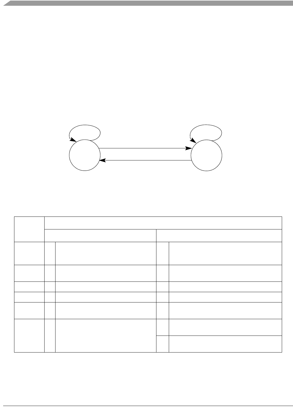
MCF548x Reference Manual, Rev. 3
7-26 Freescale Semiconductor
7.12 Cache Operation Summary
This section gives operational details for the cache and presents instruction and data cache-line state
diagrams.
7.12.1 Instruction Cache State Transitions
Because the instruction cache does not support writes, it supports fewer operations than the data cache. As
Figure 7-12 shows, an instruction cache line can be in one of two states, valid or invalid. Modified state is
not supported. Transitions are labeled with a capital letter indicating the previous state and a number
indicating the specific case listed in Table 7-6. These numbers correspond to the equivalent operations on
data caches, described in Section 7.12.2, “Data Cache State Transitions.”
Figure 7-12. Instruction Cache Line State Diagram
Table 7-6 describes the instruction cache state transitions shown in Figure 7-12.
Table 7-6. Instruction Cache Line State Transitions
Access
Current State
Invalid (V = 0) Valid (V = 1)
Read miss II1 Read line from memory and update cache;
supply data to processor;
go to valid state.
IV1 Read new line from memory and update cache;
supply data to processor; stay in valid state.
Read hit II2 Not possible IV2 Supply data to processor;
stay in valid state.
Write miss II3 Not possible IV3 Not possible
Write hit II4 Not possible IV4 Not possible
Cache
invalidate
II5 No action;
stay in invalid state.
IV5 No action;
go to invalid state.
Cache
push
II6,
II7
No action;
stay in invalid state.
IV6 No action;
go to invalid state.
IV7 No action;
stay in valid state.
Valid
V = 1
II5—ICINVA
II6—CPUSHL & IDPI
II7—CPUSHL & IDPI
IV1—CPU read miss
IV2—CPU read hit
IV7—CPUSHL & IDPI
IV5—ICINVA
IV6—CPUSHL & IDPI
Invalid
V = 0
II1—CPU read miss
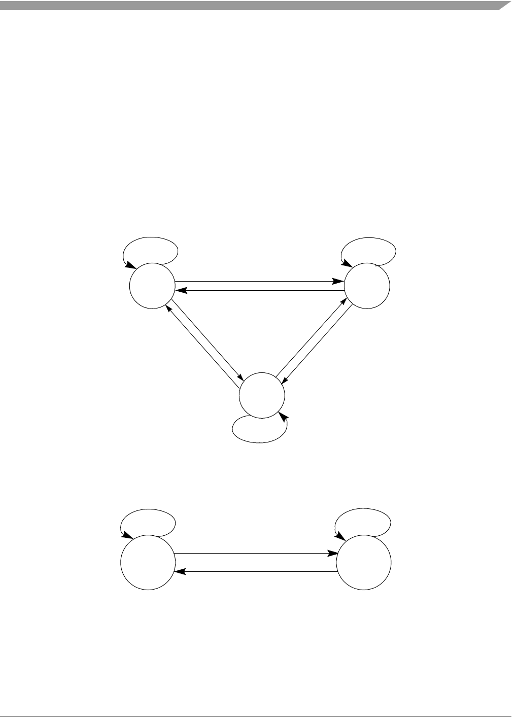
Cache Operation Summary
MCF548x Reference Manual, Rev. 3
Freescale Semiconductor 7-27
7.12.2 Data Cache State Transitions
Using the V and M bits, the data cache supports a line-based protocol allowing individual cache lines to
be invalid, valid, or modified. To maintain memory coherency, the data cache supports both write-through
and copyback modes, specified by the corresponding ACR[CM], or CACR[DDCM] if no ACR matches.
Read or write misses to copyback regions cause the cache controller to read a cache line from memory into
the cache. If available, tag and data from memory update an invalid line in the selected set. The line state
then changes from invalid to valid by setting the V bit. If all lines in the row are already valid or modified,
the pseudo-round-robin replacement algorithm selects one of the four lines and replaces the tag and data.
Before replacement, modified lines are temporarily buffered and later copied back to memory after the
new line has been read from memory.
Figure 7-13 shows the three possible data cache line states and possible processor-initiated transitions for
memory configured as copyback. Transitions are labeled with a capital letter indicating the previous state
and a number indicating the specific case; see Table 7-7.
Figure 7-13. Data Cache Line State Diagram—Copyback Mode
Figure 7-14 shows the two possible states for a cache line in write-through mode.
Figure 7-14. Data Cache Line State Diagram—Write-Through Mode
Table 7-7 describes data cache line transitions and the accesses that cause them.
Invalid
CD1—CPU
CI3—CPU
Valid
V = 1
Modified
read miss
write miss
CI5—DCINVA
CI6—CPUSHL & DDPI
CI7—CPUSHL & DDPI
CV1—CPU read miss
CV2—CPU read hit
CV7—CPUSHL & DDPI
CD2—CPU read hit
CD3—CPU write miss
CD4—CPU write hit
CD5—DCINVA
CD6—CPUSHL & DDPI CV3—CPU write miss
CV4—CPU write hit
CI1—CPU read miss
CV5—DCINVA
CV6—CPUSHL & DDPI
V = 0 M = 0
V = 1
M = 1
CD7—CPUSHL
& DDPI
WI1—CPU read miss
Invalid Valid
WI3—CPU write miss
WI5—DCINVA
WI6—CPUSHL & DDPI
WV1—CPU read miss
WV2—CPU read hit
WV3—CPU write miss
WV4—CPU write hit
WV7—CPUSHL & DDPI
WV5—DCINVA
WV6—CPUSHL & DDPI
V = 0 V = 1

MCF548x Reference Manual, Rev. 3
7-28 Freescale Semiconductor
The following tables present the same information as Table 7-7, organized by the current state of the cache
line. In Table 7-8 the current state is invalid.
Table 7-7. Data Cache Line State Transitions
Access
Current State
Invalid (V = 0) Valid (V = 1, M = 0) Modified (V = 1, M = 1)
Read
miss
(C,W)I1 Read line from
memory and update
cache;
supply data to
processor;
go to valid state.
(C,W)V1 Read new line from
memory and update
cache;
supply data to processor;
stay in valid state.
CD1 Push modified line to buffer;
read new line from memory and
update cache;
supply data to processor;
write push buffer contents to
memory;
go to valid state.
Read hit (C,W)I2 Not possible. (C,W)V2 Supply data to processor;
stay in valid state.
CD2 Supply data to processor;
stay in modified state.
Write
miss
(copy-
back)
CI3 Read line from
memory and update
cache;
write data to cache;
go to modified state.
CV3 Read new line from
memory and update
cache;
write data to cache;
go to modified state.
CD3 Push modified line to buffer;
read new line from memory and
update cache;
write push buffer contents to
memory;
stay in modified state.
Write
miss
(write-
through)
WI3 Write data to memory;
stay in invalid state.
WV3 Write data to memory;
stay in valid state.
WD3 Write data to memory;
stay in modified state.
Cache mode changed for the
region corresponding to this
line. To avoid this state, execute
a CPUSHL instruction or set
CACR[DCINVA,ICINVA] before
switching modes.
Write hit
(copy-
back)
CI4 Not possible. CV4 Write data to cache;
go to modified state.
CD4 Write data to cache;
stay in modified state.
Write hit
(write-
through)
WI4 Not possible. WV4 Write data to memory and
to cache;
stay in valid state.
WD4 Write data to memory and to
cache;
go to valid state.
Cache mode changed for the
region corresponding to this
line. To avoid this state, execute
a CPUSHL instruction or set
CACR[DCINVA,ICINVA] before
switching modes.
Cache
invalidate
(C,W)I5 No action;
stay in invalid state.
(C,W)V5 No action;
go to invalid state.
CD5 No action (modified data lost);
go to invalid state.
Cache
push
(C,W)I6
(C,W)I7
No action;
stay in invalid state.
(C,W)V6 No action;
go to invalid state.
CD6 Push modified line to memory;
go to invalid state.
(C,W)V7 No action;
stay in valid state.
CD7 Push modified line to memory;
go to valid state.

Cache Operation Summary
MCF548x Reference Manual, Rev. 3
Freescale Semiconductor 7-29
In Table 7-9 the current state is valid.
Table 7-8. Data Cache Line State Transitions (Current State Invalid)
Access Response
Read miss (C,W)I1 Read line from memory and update cache;
supply data to processor;
go to valid state.
Read hit (C,W)I2 Not possible
Write miss (copyback) CI3 Read line from memory and update cache;
write data to cache;
go to modified state.
Write miss (write-through) WI3 Write data to memory;
stay in invalid state.
Write hit (copyback) CI4 Not possible
Write hit (write-through) WI4 Not possible
Cache invalidate (C,W)I5 No action;
stay in invalid state.
Cache push (C,W)I6 No action;
stay in invalid state.
Cache push (C,W)I7 No action;
stay in invalid state.
Table 7-9. Data Cache Line State Transitions (Current State Valid)
Access Response
Read miss (C,W)V1 Read new line from memory and update cache;
supply data to processor; stay in valid state.
Read hit (C,W)V2 Supply data to processor;
stay in valid state.
Write miss (copyback) CV3 Read new line from memory and update cache;
write data to cache;
go to modified state.
Write miss (write-through) WV3 Write data to memory;
stay in valid state.
Write hit (copyback) CV4 Write data to cache;
go to modified state.
Write hit (write-through) WV4 Write data to memory and to cache;
stay in valid state.
Cache invalidate (C,W)V5 No action;
go to invalid state.
Cache push (C,W)V6 No action;
go to invalid state.
Cache push (C,W)V7 No action;
stay in valid state.

MCF548x Reference Manual, Rev. 3
7-30 Freescale Semiconductor
In Table 7-10 the current state is modified.
7.13 Cache Initialization Code
The following example sets up the cache for FLASH or ROM space only.
move.l #0xA30C8100,D0 //enable cache, invalidate it,
//default mode is cache-inhibited imprecise
movec D0, CACR
move.l #0xFF00C000,D0 //cache FLASH space, enable,
//ignore FC2, cacheable, writethrough
movec D0,ACR0
Table 7-10. Data Cache Line State Transitions (Current State Modified)
Access Response
Read miss CD1 Push modified line to buffer;
read new line from memory and update cache;
supply data to processor;
write push buffer contents to memory;
go to valid state.
Read hit CD2 Supply data to processor;
stay in modified state.
Write miss
(copyback)
CD3 Push modified line to buffer;
read new line from memory and update cache;
write push buffer contents to memory;
stay in modified state.
Write miss
(write-through)
WD3 Write data to memory;
stay in modified state.
Cache mode changed for the region corresponding to this line. To avoid this state, execute
a CPUSHL instruction or set CACR[DCINVA,ICINVA] before switching modes.
Write hit
(copyback)
CD4 Write data to cache;
stay in modified state.
Write hit
(write-through)
WD4 Write data to memory and to cache;
go to valid state.
Cache mode changed for the region corresponding to this line. To avoid this state, execute
a CPUSHL instruction or set CACR[DCINVA,ICINVA] before switching modes.
Cache invalidate CD5 No action (modified data lost);
go to invalid state.
Cache push CD6 Push modified line to memory;
go to invalid state.
Cache push CD7 Push modified line to memory;
go to valid state.
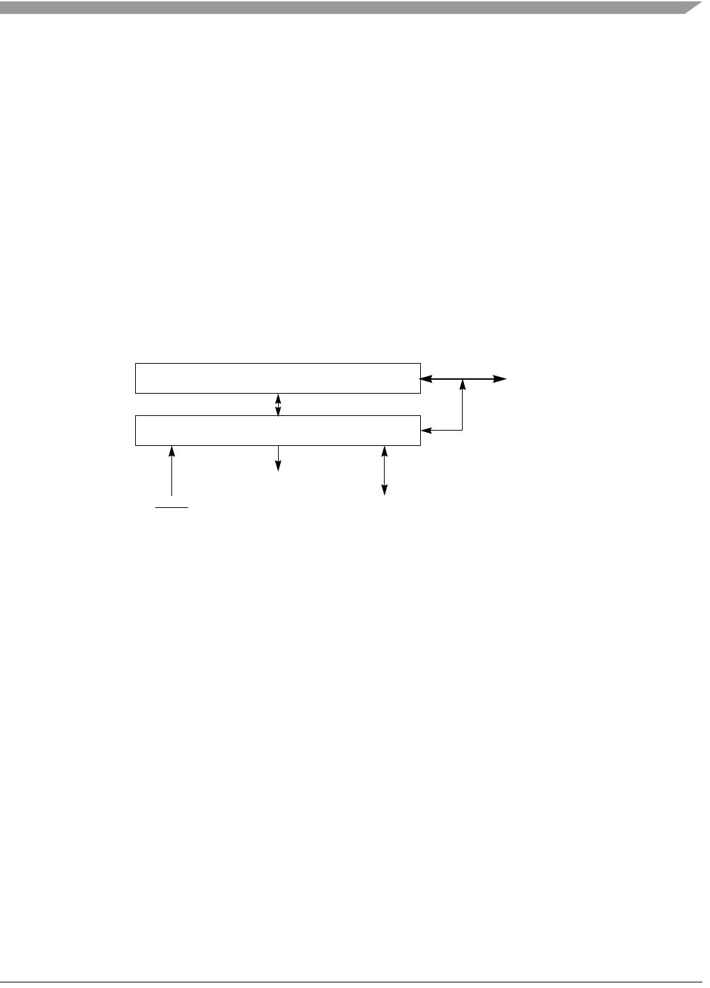
MCF548x Reference Manual, Rev. 3
Freescale Semiconductor 8-1
Chapter 8
Debug Support
8.1 Introduction
This chapter describes the Revision D enhanced hardware debug support in the ColdFire Version 4. This
revision of the ColdFire debug architecture encompasses earlier revisions. An expanded set of debug
functionality is defined as Revision B (or Rev. B). The further enhanced debug architecture implemented
in the Version 4 ColdFire is known as Revision C (or Rev. C). The addition of the memory management
unit (MMU) in the Version 4e ColdFire requires corresponding enhancements to the ColdFire debug
functionality, resulting in Revision D.
8.1.1 Overview
The debug module interface is shown in Figure 8-1.
Figure 8-1. Processor/Debug Module Interface
Debug support is divided into three areas:
• Real-time trace support: The ability to determine the dynamic execution path through an
application is fundamental for debugging. The ColdFire solution implements an 8-bit parallel
output bus that reports processor execution status and data to an external BDM emulator system.
See Section 8.3, “Real-Time Trace Support.”
• Background debug mode (BDM): Provides low-level debugging in the ColdFire processor
complex. In BDM, the processor complex is halted and a variety of commands can be sent to the
processor to access memory and registers. The external BDM emulator uses a three-pin, serial,
full-duplex channel. See Section 8.5, “Background Debug Mode (BDM),” and Section 8.4,
“Memory Map/Register Definition.”
• Real-time debug support: BDM requires the processor to be halted, which many real-time
embedded applications cannot do. Debug interrupts let real-time systems execute a unique service
routine that can quickly save key register and variable contents and return the system to normal
operation without halting. External development systems can access saved data, because the
hardware supports concurrent operation of the processor and BDM-initiated commands. In
addition, the option is provided to allow interrupts to occur. See Section 8.6, “Real-Time Debug
Support.”
The Version 2 ColdFire core implemented the original debug architecture, now called Revision A. Based
on feedback from customers and third-party developers, enhancements have been added to succeeding
ColdFire CPU Core
Debug Module
High-speed
Communication Port
DSCLK, DSI, DSO
Control
BKPT
local bus
Tra ce Por t
PSTDDATA[7:0]
PSTCLK

MCF548x Reference Manual, Rev. 3
8-2 Freescale Semiconductor
generations of ColdFire cores. For Revision A, CSR[HRL] is 0. See Section 8.4.2, “Configuration/Status
Register (CSR).”
The Version 3 core implements Revision B of the debug architecture, offering more flexibility for
configuring the hardware breakpoint trigger registers and removing the restrictions involving concurrent
BDM processing while hardware breakpoint registers are active. For Revision B, CSR[HRL] is 1.
Revision C of the debug architecture more than doubles the on-chip breakpoint registers and provides an
ability to interrupt debug service routines. For Revision C, CSR[HRL] is 2.
Differences between Revision B and C are summarized as follows:
• Debug Revision B has separate PST[3:0] and DDATA[3:0] signals.
• Debug Revision C adds breakpoint registers and supports normal interrupt request service during
debug. It combines debug signals into PSTDDATA[7:0].
The addition of the memory management unit (MMU) to the baseline architecture requires corresponding
enhancements to the ColdFire debug functionality, resulting in Revision D. For Revision D, the revision
level bit, CSR[HRL], is 3.
With software support, the MMU can provide a demand-paged, virtual address environment. To support
debugging in this virtual environment, the debug enhancements are primarily related to the expansion of
the virtual address to include the 8-bit address space identifier (ASID). Conceptually, the virtual address
is expanded to a 40-bit value: the 8-bit ASID plus the 32-bit address.
The expansion of the virtual address affects two major debug functions:
• The ASID is optionally included in the specification of the hardware breakpoint registers. As an
example, the four PC breakpoint registers are each expanded by 8 bits, so that a specific ASID
value may be programmed as part of the breakpoint instruction address. Likewise, each operand
address/data breakpoint register is expanded to include an ASID value. Finally, new control
registers define if and how the ASID is to be included in the breakpoint comparison trigger logic.
• The debug module implements the concept of ownership trace in which the ASID value may be
optionally displayed as part of the real-time trace functionality. When enabled, real-time trace
displays instruction addresses on every change-of-flow instruction that is not absolute or
PC-relative. For Rev. D, this instruction address display optionally includes the contents of the
ASID, thus providing the complete instruction virtual address on these instructions.
Additionally when a Sync_PC serial BDM command is loaded from the external development
system, the processor optionally displays the complete virtual instruction address, including the
8-bit ASID value.
In addition to these ASID-related changes, the new MMU control registers are accessible by using serial
BDM commands. The same BDM access capabilities are also provided for the EMAC and FPU
programming models.
Finally, a new serial BDM command is implemented (FORCE_TA) to assist debugging when a software
error generates an incorrect memory address that hangs the external bus. The new BDM command
attempts to break this condition by forcing a bus termination.
8.2 Signal Descriptions
Table 8-1 describes debug module signals. All ColdFire debug signals are unidirectional and related to a
rising edge of the processor core’s clock signal. The standard 26-pin debug connector is shown in
Section 8.9, “Freescale-Recommended BDM Pinout.”
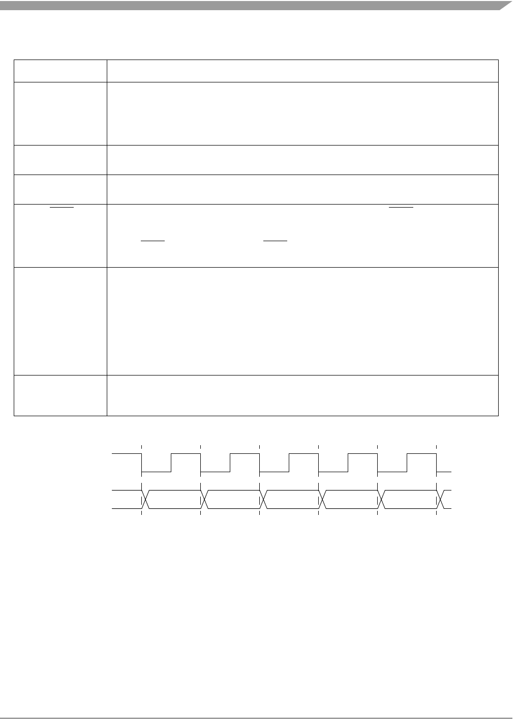
Signal Descriptions
MCF548x Reference Manual, Rev. 3
Freescale Semiconductor 8-3
Figure 8-2 shows PSTCLK timing with respect to PSTDDATA.
Figure 8-2. PSTCLK Timing
8.2.1 Processor Status/Debug Data (PSTDDATA[7:0])
Processor status data outputs are used to indicate both processor status and captured address and data
values. They operate at half the processor’s frequency. Given that real-time trace information appears as a
sequence of 4-bit data values, there are no alignment restrictions; that is, the processor status (PST) values
and operands may appear on either nibble of PSTDDATA[7:0]. The upper nibble (PSTDDATA[7:4]) is the
more significant and yields values first.
CSR controls capturing of data values to be presented on PSTDDATA. Executing the WDDATA
instruction captures data that is displayed on PSTDDATA too. These signals are updated each processor
cycle and display two values at a time for two processor clock cycles. Table 8-2 shows the PSTDDATA
Table 8-1. Debug Module Signals
Signal Description
DSCLK Development Serial Clock-Internally synchronized input. (The logic level on DSCLK is validated
if it has the same value on two consecutive rising bus clock edges.) Clocks the serial
communication port to the debug module during packet transfers. Maximum frequency is
PSTCLK/5. At the synchronized rising edge of DSCLK, the data input on DSI is sampled and
DSO changes state.
DSI Development Serial Input -Internally synchronized input that provides data input for the serial
communication port to the debug module, once the DSCLK has been seen as high (logic 1).
DSO Development Serial Output -Provides serial output communication for debug module responses.
DSO is registered internally. The output is delayed from the validation of DSCLK high.
BKPT Breakpoint - Input used to request a manual breakpoint. Assertion of BKPT puts the processor
into a halted state after the current instruction completes. Halt status is reflected on processor
status/debug data signals (PSTDDATA[7:0]) as the value 0xF. If CSR[BKD] is set (disabling
normal BKPT functionality), asserting BKPT generates a debug interrupt exception in the
processor.
PSTCLK Processor Status Clock - Half-speed version of the processor clock. Its rising edge appears in the
center of the two-processor-cycle window of valid PSTDDATA output. See Figure 8-2. PSTCLK
indicates when the development system should sample PSTDDATA values.
If real-time trace is not used, setting CSR[PCD] keeps PSTCLK and PSTDDATA outputs from
toggling without disabling triggers. Non-quiescent operation can be reenabled by clearing
CSR[PCD], although the external development systems must resynchronize with the PSTDDATA
output.
PSTCLK starts clocking only when the first non-zero PST value (0xC, 0xD, or 0xF) occurs during
system reset exception processing. Tabl e 8-4 describes PST values.
PSTDDATA[7:0] Processor Status/Debug Data - These outputs, which change on the negative edge of PSTCLK,
indicate both processor status and captured address and data values and are discussed more
thoroughly in Section 8.2.1, “Processor Status/Debug Data (PSTDDATA[7:0]).”
PSTCLK
S
TDDATA
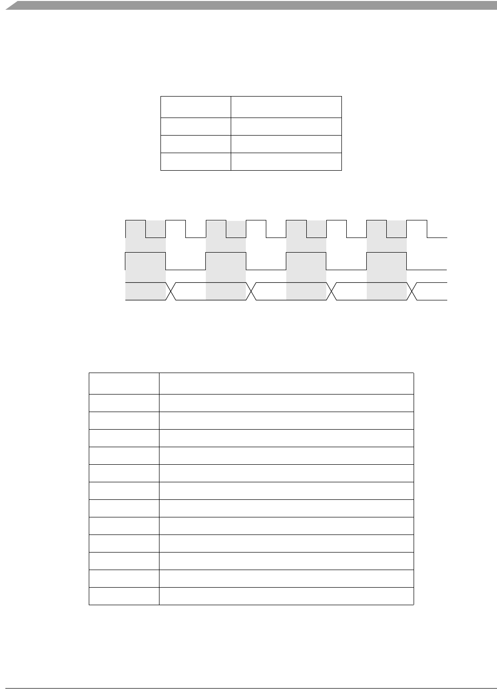
MCF548x Reference Manual, Rev. 3
8-4 Freescale Semiconductor
output for the processor’s sequential execution of single-cycle instructions (A, B, C, D...). Cycle counts
are shown relative to processor frequency. These outputs indicate the current processor pipeline status and
are not related to the current bus transfer.
The signal timing for the example in Table 8-2 is shown in Figure 8-3.
Figure 8-3. PSTDDATA: Single-Cycle Instruction Timing
Table 8-3 shows the case where a PSTDDATA module captures a memory operand on a simple load
instruction: mov.l <mem>,Rx.
Table 8-2. PSTDDATA: Sequential Execution of Single-Cycle Instructions
Cycles PSTDDATA[7:0]
T+0, T+1 {PST for A, PST for B}
T+2, T+3 {PST for C, PST for D}
T+4, T+5 {PST for E, PST for F}
Table 8-3. PSTDDATA: Data Operand Captured
Cycle PSTDDATA[7:0]
T {PST for mov.l, PST marker for captured operand) = {0x1, 0xB}
T+1 {0x1, 0xB}
T+2 {Operand[3:0], Operand[7:4]}
T+3 {Operand[3:0], Operand[7:4]}
T+4 {Operand[11:8], Operand[15:12]}
T+5 {Operand[11:8], Operand[15:12]}
T+6 {Operand[19:16], Operand[23:20]}
T+7 {Operand[19:16], Operand[23:20]}
T+8 {Operand[27:24], Operand[31:28]}
T+9 {Operand[27:24], Operand[31:28]}
T+10 (PST for next instruction)
T+11 (PST for next instruction,...)
PSTDDATA
PSTCLK
{A, B} {C, D} {E, F}
Processor Clock
T+0 T+1 T+2 T+3 T+4 T+5 T+6

Real-Time Trace Support
MCF548x Reference Manual, Rev. 3
Freescale Semiconductor 8-5
NOTE
A PST marker and its data display are sent contiguously. Except for this
transmission, the IDLE status (0x0) can appear anytime. Again, given that
real-time trace information appears as a sequence of 4-bit values, there are
no alignment restrictions. That is, PST values and operands may appear on
either nibble of PSTDDATA.
8.3 Real-Time Trace Support
Real-time trace, which defines the dynamic execution path, is a fundamental debug function. The ColdFire
solution is to include a parallel output port providing encoded processor status and data to an external
development system. This 8-bit port is partitioned into two consecutive 4-bit nibbles. Each nibble can
either transmit information concerning the processor’s execution status (PST) or debug data (DDATA).
The processor status may not be related to the current bus transfer, due to the decoupling FIFOs.
External development systems can use PSTDDATA outputs with an external image of the program to
completely track the dynamic execution path. This tracking is complicated by any change in flow,
especially when branch target address calculation is based on the contents of a program-visible register
(variant addressing). PSTDDATA outputs can be configured to display the target address of such
instructions in sequential nibble increments across multiple processor clock cycles, as described in
Section 8.3.1, “Begin Execution of Taken Branch (PST = 0x5).” Four 32-bit storage elements form a FIFO
buffer connecting the processor’s high-speed local bus to the external development system through
PSTDDATA[7:0]. The buffer captures branch target addresses and certain data values for eventual display
on the PSTDDATA port, two nibbles at a time starting with the least significant bit (lsb).
Execution speed is affected only when three storage elements contain valid data to be dumped to the
PSTDDATA port. This occurs only when two values are captured simultaneously in a read-modify-write
operation. The core stalls until two FIFO entries are available.
Table 8-4 shows the encoding of these signals.
Table 8-4. Processor Status Encoding
PST[3:0]
Definition
Hex Binary
0x0 0000 Continue execution. Many instructions execute in one processor cycle. If an instruction requires
more clock cycles, subsequent clock cycles are indicated by driving PSTDDATA outputs with this
encoding.
0x1 0001 Begin execution of one instruction. For most instructions, this encoding signals the first clock cycle
of an instruction’s execution. Certain change-of-flow opcodes, plus the PULSE and WDDATA
instructions, generate different encodings.
0x2 0010 Begin execution of two instructions. For superscalar instruction dispatches, this encoding signals the
first clock cycle of the simultaneous instructions’ execution.
0x3 0011 Entry into user-mode. Signaled after execution of the instruction that caused the ColdFire processor
to enter user mode. If the display of the ASID is enabled (CSR[3] = 1), the following occurs:
• The 8-bit ASID follows the instruction address; that is, the PSTDDATA sequence is {0x3, 0x5,
marker, instruction address, 0x8, ASID}, where 0x8 is the ASID data marker.
• Whenever the current ASID is loaded by the privileged MOVEC instruction, the ASID is displayed
on PSTDDATA. The resulting PSTDDATA sequence for the MOVEC instruction is then {0x1, 0x8,
ASID}, where the 0x8 is the data marker for the ASID.

MCF548x Reference Manual, Rev. 3
8-6 Freescale Semiconductor
8.3.1 Begin Execution of Taken Branch (PST = 0x5)
PST is 0x5 when a taken branch is executed. For some opcodes, a branch target address may be displayed
on PSTDDATA depending on the CSR settings. CSR also controls the number of address bytes displayed,
which is indicated by the PST marker value immediately preceding the PSTDDATA nibble that begins the
data output.
Multiple byte DDATA values are displayed in least-to-most-significant order. The processor captures only
those target addresses associated with taken branches which use a variant addressing mode, that is, RTE
and RTS instructions, JMP and JSR instructions using address register indirect or indexed addressing
modes, and all exception vectors.
0x4 0100 Begin execution of PULSE and WDDATA instructions. PULSE defines logic analyzer triggers for
debug or performance analysis. WDDATA lets the core write any operand (byte, word, or longword)
directly to the PSTDDATA port, independent of debug module configuration. When WDDATA is
executed, a value of 0x4 is signaled, followed by the appropriate marker, and then the data transfer
on the PSTDDATA port. Transfer length depends on the WDDATA operand size.
0x5 0101 Begin execution of taken branch or SYNC_PC command. For some opcodes, a branch target
address may be displayed on PSTDDATA depending on the CSR settings. CSR also controls the
number of address bytes displayed, indicated by the PST marker value preceding the DDATA nibble
that begins the data output. See Section 8.3.1, “Begin Execution of Taken Branch (PST = 0x5).” Also
indicates that the SYNC_PC command has been issued.
0x6 0110 Begin execution of instruction plus a taken branch. The processor completes execution of a taken
conditional branch instruction and simultaneously starts executing the target instruction. This is
achieved through branch folding.
0x7 0111 Begin execution of return from exception (RTE) instruction.
0x8–0xB 1000–1011 Indicates the number of bytes to be displayed on the DDATA port on subsequent clock cycles. The
value is driven onto the PSTDDATA port one cycle before the data is displayed.
0x8 Begin 1-byte transfer on PSTDDATA.
0x9 Begin 2-byte transfer on PSTDDATA.
0xA Begin 3-byte transfer on PSTDDATA.
0xB Begin 4-byte transfer on PSTDDATA.
0xC 1100 Normal exception processing. Exceptions that enter emulation mode (debug interrupt or optionally
trace) generate a different encoding, as described below. Because the 0xC encoding defines a
multiple-cycle mode, PSTDDATA outputs are driven with 0xC until exception processing completes.
0xD 1101 Emulator mode exception processing. Displayed during emulation mode (debug interrupt or
optionally trace). Because this encoding defines a multiple-cycle mode, PSTDDATA outputs are
driven with 0xD until exception processing completes.
0xE 1110 A breakpoint state change causes this encoding to assert for one cycle only followed by the trigger
status value. If the processor stops waiting for an interrupt, the encoding is asserted for multiple
cycles. See Section 8.3.2, “Processor Stopped or Breakpoint State Change (PST = 0xE).”
0xF 1111 Processor is halted. Because this encoding defines a multiple-cycle mode, the PSTDDATA outputs
display 0xF until the processor is restarted or reset. (see Section 8.5.1, “CPU Halt”)
Table 8-4. Processor Status Encoding (Continued)
PST[3:0]
Definition
Hex Binary
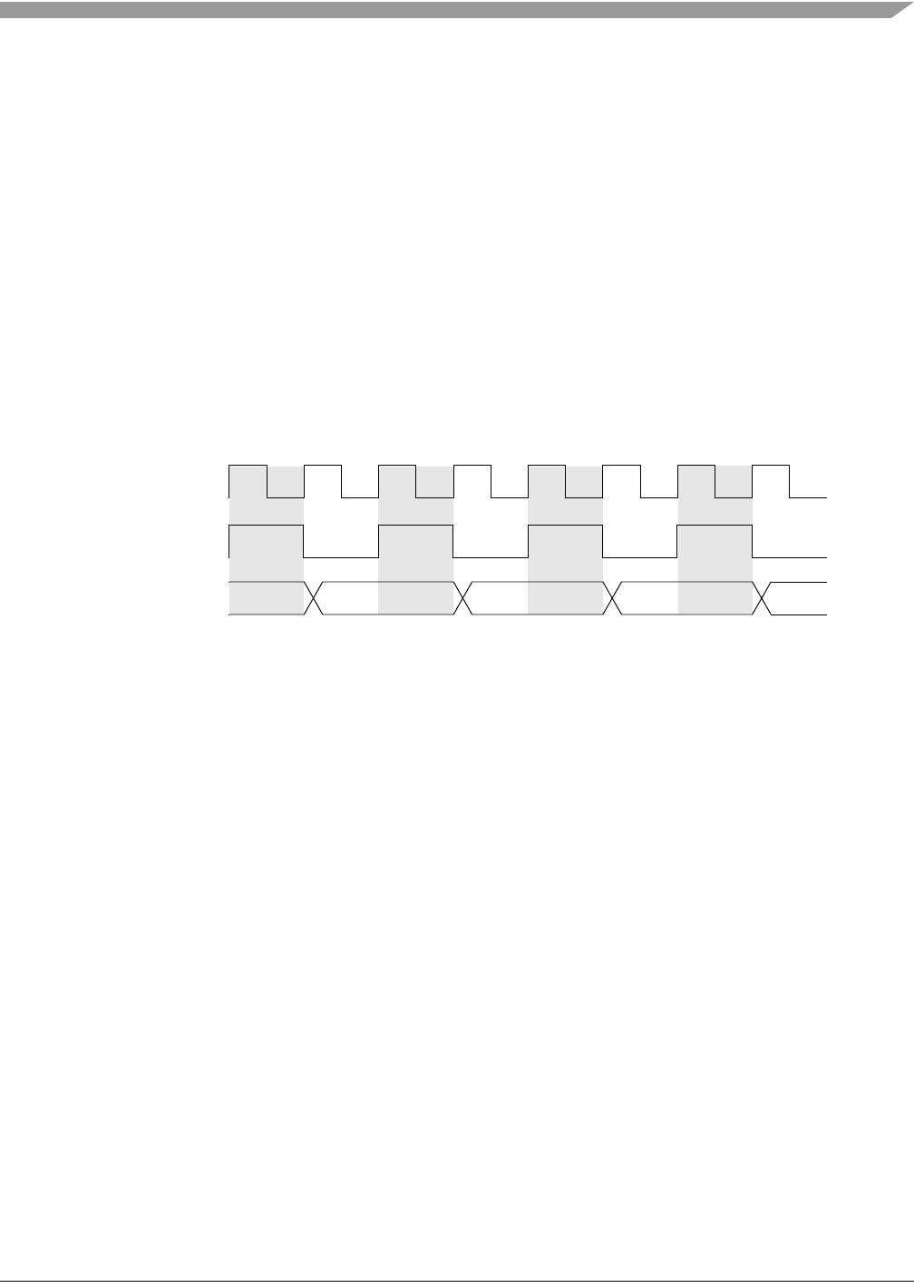
Real-Time Trace Support
MCF548x Reference Manual, Rev. 3
Freescale Semiconductor 8-7
The simplest example of a branch instruction using a variant address is the compiled code for a C language
case statement. Typically, the evaluation of this statement uses the variable of an expression as an index
into a table of offsets, where each offset points to a unique case within the structure. For such
change-of-flow operations, the V4 microarchitecture uses the debug pins to output the following sequence
of information on two successive processor clock cycles:
1. Use PSTDDATA (0x5) to identify that a taken branch is executed.
2. Optionally signal the target address to be displayed sequentially on the PSTDDATA pins.
Encodings 0x9–0xB identify the number of bytes displayed.
3. The new target address is optionally available on subsequent cycles using the PSTDDATA port.
The number of bytes of the target address displayed on this port is configurable (2, 3, or 4 bytes,
where the encoding is 0x9, 0xA, and 0xB, respectively).
Another example of a variant branch instruction would be a JMP (A0) instruction. Figure 8-4 shows when
the PSTDDATA outputs that indicate when a JMP (A0) executed, assuming the CSR was programmed to
display the lower 2 bytes of an address.
Figure 8-4. Example JMP Instruction Output on PSTDDATA
PSTDDATA is driven two nibbles at a time with a 0x59; 0x5 indicates a taken branch and the marker value
0x9 indicates a 2-byte address. Thus, the subsequent 4 nibbles display the lower 2 bytes of address register
A0 in least-to-most-significant nibble order. The PSTDDATA output after the JMP instruction continues
with the next instruction.
8.3.2 Processor Stopped or Breakpoint State Change (PST = 0xE)
The 0xE encoding is generated either as a one- or multiple-cycle issue as follows:
• When the core is stopped by a STOP instruction, this encoding appears in multiple-cycle format.
The ColdFire processor remains stopped until an interrupt occurs; thus, PSTDDATA outputs
display 0xE until stopped mode is exited.
• When a breakpoint status change is to be output on PSTDDATA, 0xE is displayed for one cycle,
followed immediately with the 4-bit value of the current trigger status, where the trigger status is
left justified rather than in the CSR[BSTAT] description. Section 8.4.2, “Configuration/Status
Register (CSR),” shows that status is right justified. That is, the displayed trigger status on
PSTDDATA after a single 0xE is as follows:
— 0x0 = no breakpoints enabled
— 0x2 = waiting for level-1 breakpoint
— 0x4 = level-1 breakpoint triggered
— 0xA = waiting for level-2 breakpoint
— 0xC = level-2 breakpoint triggered
Thus, 0xE can indicate multiple events, based on the next value, as Table 8-5 shows.
PSTDDATA
PSTCLK
0x59 A0[3–0,7–4] A0[11–8,15–12]
Processor Clock

MCF548x Reference Manual, Rev. 3
8-8 Freescale Semiconductor
8.3.3 Processor Halted (PST = 0xF)
PST is 0xF when the processor is halted (see Section 8.5.1, “CPU Halt”). Because this encoding defines a
multiple-cycle mode, the PSTDDATA outputs display 0xF until the processor is restarted or reset.
Therefore, PSTDDATA[7:0] continuously are 0xFF.
NOTE
HALT can be distinguished from a data output 0xFF by counting 0xFF
occurrences on PSTDDATA. Because data always follows a marker (0x8,
0x9, 0xA, or 0xB), the longest occurrence in PSTDDATA of 0xFF in a data
output is four.
Two scenarios exist for data 0xFFFF_FFFF:
• The B marker occurs on the most-significant nibble of PSTDDATA with the data of 0xFF
following:
PSTDDATA[7:0]
0xBF
0xFF
0xFF
0xFF
0xFX (X indicates that the next PST value is guaranteed to not be 0xF.)
• The B marker occurs on the least-significant nibble of PSTDDATA with the data of 0xFF
following:
PSTDDATA[7:0]
0xYB
0xFF
0xFF
0xFF
0xFF
0xXY (X indicates the PST value is guaranteed not to be 0xF, and Y signifies a PSTDDATA
value that doesn’t affect the 0xFF count.)
NOTE
As the result of the above, a count of at least nine or more sequential single
0xF values or five or more sequential 0xFF values indicates the HALT
condition.
Table 8-5. 0xE Status Posting
PSTDDATA Stream Includes Result
{0xE, 0x2} Breakpoint state changed to waiting for level-1 trigger
{0xE, 0x4} Breakpoint state changed to level-1 breakpoint triggered
{0xE, 0xA} Breakpoint state changed to waiting for level-2 trigger
{0xE, 0xC} Breakpoint state changed to level-2 breakpoint triggered
{0xE, 0xE} Stopped mode.

Memory Map/Register Definition
MCF548x Reference Manual, Rev. 3
Freescale Semiconductor 8-9
8.4 Memory Map/Register Definition
In addition to the existing BDM commands that provide access to the processor’s registers and the memory
subsystem, the debug module contains 19 registers to support the required functionality. These registers
are also accessible from the processor’s supervisor programming model by executing the WDEBUG
instruction (write only). Thus, the breakpoint hardware in the debug module can be read or written by the
external development system using the debug serial interface or written by the operating system running
on the processor core. Software is responsible for guaranteeing that accesses to these resources are
serialized and logically consistent. Hardware provides a locking mechanism in the CSR to allow the
external development system to disable any attempted writes by the processor to the breakpoint registers
(setting CSR[IPW]). BDM commands must not be issued if the WDEBUG instruction is used to access
debug module registers or the resulting behavior is undefined.
These registers, shown in Figure 8-5, are treated as 32-bit quantities, regardless of the number of
implemented bits.
Figure 8-5. Debug Programming Model
ABLR1
ABHR1
AATR1
PC breakpoint 1 register
PC breakpoint 3 register
PC breakpoint mask register
PC breakpoint register
Data breakpoint register
Data breakpoint mask register
Data breakpoint 1 register
Data breakpoint mask 1 register
Trigger definition register
Extended trigger definition registerXTDR
Configuration/status register
BDM address attributes register
PC breakpoint 2 register
Note: Each debug register is accessed as a 32-bit register; shaded fields above are not used (don’t care).
All debug control registers are writable from the external development system or the CPU via the WDEBUG
instruction.
CSR is write-only from the programming model. It can be read from and written to through the BDM port.
CSR is accessible in supervisor mode as debug control register 0x00 using the WDEBUG instruction and
Address attribute trigger register
Address low breakpoint register
Address high breakpoint register
Address 1 attribute trigger register
Address low breakpoint 1 register
Address high breakpoint 1 register
31 15 7 0
31 15 7 0
31 15 7 0
31 15 0
31 15 0
31 15 0
31 15 0
31 15
31 15 0
31 15 0
31 15 0
31 15 0
31 15 0
31 15 0
AATR
ABLR
ABHR
BAAR
CSR
DBR
DBMR
PBR
DBR1
DBMR1
PBR1
PBR2
PBR3
PBMR
TDR

MCF548x Reference Manual, Rev. 3
8-10 Freescale Semiconductor
The registers in Table 8-7 are accessed through the BDM port by BDM commands, WDMREG and RDMREG,
described in Section 8.5.3.3, “Command Set Descriptions.” These commands contain a 5-bit field, DRc,
that specifies the register, as shown in Table 8-6.
These registers are also accessible from the processor’s supervisor programming model through the
execution of the WDEBUG instruction. Thus, the external development system and the operating system
running on the processor core can access the breakpoint hardware. It is the responsibility of the software
Table 8-6. BDM/Breakpoint Registers
DRc[4–0] Register Name Abbreviation Initial State Section/
Page
0x00 Configuration/status register1
1CSR is write-only from the programming model. It can be read or written through the BDM port using the
RDMREG and WDMREG commands.
CSR 0x0020_0000 8.4.2/8-11
0x01–0x05 Reserved — — —
0x04 PC breakpoint ASID control PBAC — 8.4.3/8-14
0x05 BDM address attribute register BAAR 0x0000_0005 8.4.4/8-15
0x06 Address attribute trigger register AATR 0x0000_0005 8.4.5/8-16
0x07 Trigger definition register TDR 0x0000_0000 8.4.6/8-17
0x08 Program counter breakpoint register PBR — 8.4.7/8-20
0x09 Program counter breakpoint mask register PBMR — 8.4.7/8-20
0x0A–0x0B Reserved — — —
0x0C Address breakpoint high register ABHR — 8.4.8/8-21
0x0D Address breakpoint low register ABLR — 8.4.8/8-21
0x0E Data breakpoint register DBR — 8.4.9/8-22
0x0F Data breakpoint mask register DBMR — 8.4.9/8-22
0x10–0x153 Reserved — — —
0x14 PC breakpoint ASID register PBASID — 8.4.10/8-24
0x15 Reserved — — —
0x16 Address attribute trigger register 1 AATR1 0x0000_0005 8.4.5/8-16
0x17 Extended trigger definition register XTDR 0x0000_0000 8.4.11/8-25
0x18 Program counter breakpoint 1 register PBR1 0x0000_0000 8.4.7/8-20
0x19 Reserved — — —
0x1A Program counter breakpoint register 2 PBR2 0x0000_0000 8.4.7/8-20
0x1B Program counter breakpoint register 3 PBR3 0x0000_0000 8.4.7/8-20
0x1C Address high breakpoint register 1 ABHR1 — 8.4.8/8-21
0x1D Address low breakpoint register 1 ABLR1 — 8.4.8/8-21
0x1E Data breakpoint register 1 DBR1 — 8.4.9/8-22
0x1F Data breakpoint mask register 1 DBMR1 — 8.4.9/8-22

Memory Map/Register Definition
MCF548x Reference Manual, Rev. 3
Freescale Semiconductor 8-11
to guarantee that all accesses to these resources are serialized and logically consistent. The hardware
provides a locking mechanism in the CSR to allow the external development system to disable any
attempted writes by the processor to the breakpoint registers (setting IPW = 1). BDM commands must not
be issued if the ColdFire processor is accessing debug module registers with the WDEBUG instruction or
the resulting behavior is undefined.
The ColdFire debug architecture supports a number of hardware breakpoint registers, that can be
configured into single- or double-level triggers based on the PC or operand address ranges with an optional
inclusion of specific data values. With the addition of the MMU capabilities, the breakpoint specifications
must be expanded to optionally include the address space identifier (ASID) in these user-programmable
virtual address triggers.
The core includes four PC breakpoint triggers and two sets of operand address breakpoint triggers, each
with two independent address registers (to allow specification of a range) and a data breakpoint with
masking capabilities. Core breakpoint triggers are accessible through the serial BDM interface or written
through the supervisor programming model using the WDEBUG instruction.
Two ASID-related registers (PBAC and PBASID) are added for the PC breakpoint qualification, and two
existing registers (AATR and AATR1) are expanded for the address breakpoint qualification.
8.4.1 Revision A Shared Debug Resources
In the Revision A implementation of the debug module, certain hardware structures are shared between
BDM and breakpoint functionality, as shown in Table 8-7.
Thus, loading a register to perform a specific function that shares hardware resources is destructive to the
shared function. For example, a BDM command to access memory overwrites an address breakpoint in
ABHR. A BDM write command overwrites the data breakpoint in DBR.
Revision B added hardware registers to eliminate these shared functions. The BAAR is used to specify bus
attributes for BDM memory commands and has the same format as the LSB of the AATR. Note that the
registers containing the BDM memory address and the BDM data are not program visible.
8.4.2 Configuration/Status Register (CSR)
The configuration/status register (CSR) defines the debug configuration for the processor and memory
subsystem and contains status information from the breakpoint logic. CSR is write-only from the
programming model. CSR is accessible in supervisor mode as debug control register 0x00 using the
WDEBUG instruction and through the BDM port using the RDMREG and WDMREG commands. It can
be read from and written to through the BDM port.
Table 8-7. Rev. A Shared BDM/Breakpoint Hardware
Register BDM Function Breakpoint Function
AATR Bus attributes for all memory commands Attributes for address breakpoint
ABHR Address for all memory commands Address for address breakpoint
DBR Data for all BDM write commands Data for data breakpoint

MCF548x Reference Manual, Rev. 3
8-12 Freescale Semiconductor
Table 8-8 describes CSR fields.
31 30 29 28 27 26 25 24 23 22 21 20 19 18 17 16
R BSTAT FOF TRG HALT BKPT HRL 0 BKD0 PCD0 IPW0
W
Reset000000 0 0 001000 0 0
15 14 13 12 11 10 9 8 7 6 5 4 3 2 1 0
R MAP TRC EMU DDC UHE BTB 0 NPL 0 SSM OTE 0 0 0
W
Reset000000 0 0 000000 0 0
Reg
Addr
CPU + 0x00
Figure 8-6. Configuration/Status Register (CSR)
Table 8-8. CSR Field Descriptions
Bits Name Description
31–28 BSTAT Breakpoint status. Provides read-only status information concerning hardware breakpoints. Also
output on PSTDDATA when it is not displaying PST or other processor data. BSTAT is cleared by a
TDR or XTDR write or by a CSR read when either a level-2 breakpoint is triggered or a level-1
breakpoint is triggered and the level-2 breakpoint is disabled.
0000 No breakpoints enabled
0001 Waiting for level-1 breakpoint
0010 Level-1 breakpoint triggered
0101 Waiting for level-2 breakpoint
0110 Level-2 breakpoint triggered
27 FOF Fault-on-fault. If FOF is set, a catastrophic halt occurred and forced entry into BDM.
26 TRG Hardware breakpoint trigger. If TRG is set, a hardware breakpoint halted the processor core and
forced entry into BDM. Reset, and the debug GO command clear TRG.
25 HALT Processor halt. If HALT is set, the processor executed a HALT and forced entry into BDM. Reset,
and the debug GO command clear HALT.
24 BKPT Breakpoint assert. If BKPT is set, BKPT is asserted, forcing the processor into BDM. Reset, and
the debug GO command clear BKPT.
23–20 HRL Hardware revision level. Indicates the level of debug module functionality. An emulator could use
this information to identify the level of functionality supported.
0000 Initial debug functionality (Revision A)
0001 Revision B
0010 Revision C
0011 Revision D
19 — Reserved, should be cleared.

Memory Map/Register Definition
MCF548x Reference Manual, Rev. 3
Freescale Semiconductor 8-13
18 BKD Breakpoint disable. Used to disable the normal BKPT input functionality and to allow the assertion
of BKPT to generate a debug interrupt.
0 Normal operation
1 BKPT is edge-sensitive: a high-to-low edge on BKPT signals a debug interrupt to the processor.
The processor makes this interrupt request pending until the next sample point, when the
exception is initiated. In the ColdFire architecture, the interrupt sample point occurs once per
instruction. There is no support for nesting debug interrupts.
17 PCD PSTCLK disable. Setting PCD disables generation of PSTCLK and PSTDDATA outputs and forces
them to remain quiescent.
16 IPW Inhibit processor writes. Setting IPW inhibits processor-initiated writes to the debug module’s
programming model registers. IPW can be modified only by commands from the external
development system.
15 MAP Force processor references in emulator mode.
0 All emulator-mode references are mapped into supervisor code and data spaces.
1 The processor maps all references while in emulator mode to a special address space, TT = 10,
TM = 101 or 110. The internal SRAM and caches are disabled.
14 TRC Force emulation mode on trace exception. If TRC = 1, the processor enters emulator mode when a
trace exception occurs. If TRC=0, the processor enters supervisor mode.
13 EMU Force emulation mode. If EMU = 1, the processor begins executing in emulator mode. See
Section 8.6.1.1, “Emulator Mode.”
12–11 DDC Debug data control. Controls operand data capture for PSTDDATA, which displays the number of
bytes defined by the operand reference size before the actual data; byte displays 8 bits, word
displays 16 bits, and long displays 32 bits (one nibble at a time across multiple clock cycles). See
Table 8-4.
00 No operand data is displayed.
01 Capture all write data.
10 Capture all read data.
11 Capture all read and write data.
10 UHE User halt enable. Selects the CPU privilege level required to execute the HALT instruction.
0 HALT is a supervisor-only instruction.
1 HALT is a supervisor/user instruction.
9–8 BTB Branch target bytes. Defines the number of bytes of branch target address PSTDDATA displays.
00 0 bytes
01 Lower 2 bytes of the target address
10 Lower 3 bytes of the target address
11 Entire 4-byte target address
See Section 8.3.1, “Begin Execution of Taken Branch (PST = 0x5).”
7 — Reserved, should be cleared.
Table 8-8. CSR Field Descriptions (Continued)
Bits Name Description

MCF548x Reference Manual, Rev. 3
8-14 Freescale Semiconductor
8.4.3 PC Breakpoint ASID Control Register (PBAC)
The PBAC configures the breakpoint qualification for each PC breakpoint register (PBR, PBR1, PBR2,
and PBR3). Four bits are dedicated for each breakpoint register and specify how the ASID is used in PC
breakpoint qualification.
PBR3AC, PBR2AC, PBR1AC, and PBRAC apply to PBR3, PBR2, PBR1, and PBR, respectively, and are
functionally identical. They enable or disable ASID, supervisor mode, and user mode breakpoint
6 NPL Non-pipelined mode. Determines whether the core operates in pipelined or mode.
0 Pipelined mode
1 Non-pipelined mode. The processor effectively executes one instruction at a time with no overlap.
This adds at least 5 cycles to the execution time of each instruction. Superscalar instruction
dispatch is disabled when operating in this mode. Given an average execution latency of 1.6,
throughput in non-pipeline mode would be 6.6, approximately 25% or less of pipelined
performance.
Regardless of the NPL state, a triggered PC breakpoint is always reported before the triggering
instruction executes. In normal pipeline operation, the occurrence of an address or data breakpoint
trigger is imprecise. In non-pipeline mode, triggers are always reported before the next instruction
begins execution and trigger reporting can be considered precise.
An address or data breakpoint should always occur before the next instruction begins execution.
Therefore, the occurrence of the address/data breakpoints should be guaranteed.
5 — Reserved, should be cleared.
4 SSM Single-step mode. Setting SSM puts the processor in single-step mode.
0 Normal mode.
1 Single-step mode. The processor halts after execution of each instruction. While halted, any
BDM command can be executed. On receipt of the GO command, the processor executes the
next instruction and halts again. This process continues until SSM is cleared.
3 OTE Ownership-trace enable.
1 The display of the ASID on the PSTDDATA outputs by entering in user mode, by loading the
ASID by a MOVEC, or by executing a BDM SYNC_PC command.
3–0 — Reserved, should be cleared.
31 30 29 28 27 26 25 24 23 22 21 20 19 18 17 16
R0 0 0 0 0 0 0 0 0 0 0 0 0 0 0 0
W
Reset 0 0 0 0 0 0 0 0 0 0 0 0 0 0 0 0
15 14 13 12 11 10 9 8 7 6 5 4 3 2 1 0
R PBR3AC PBR2AC PBR1AC PBRAC
W
Reset 0 0 0 0 0 0 0 0 0 0 0 0 0 0 0 0
Reg
Addr
CPU + 0x0A
Figure 8-7. PC Breakpoint ASID Control Register (PBAC)
Table 8-8. CSR Field Descriptions (Continued)
Bits Name Description

Memory Map/Register Definition
MCF548x Reference Manual, Rev. 3
Freescale Semiconductor 8-15
qualification. Reset clears these fields, disabling qualifications and defaulting to the Revision C debug
module functionality.
8.4.4 BDM Address Attribute Register (BAAR)
The BAAR defines the address space for memory-referencing BDM commands. To maintain
compatibility with Revision A, BAAR is loaded with any data written to the LSB of AATR. See
Figure 8-8. The reset value of 0x5 sets supervisor data as the default address space.
BAAR is write only. BAAR[R,SZ] are loaded directly from the BDM command. BAAR[TT,TM] can be
programmed as debug control register 0x05 from the external development system. For compatibility with
Rev. A, BAAR is loaded each time AATR is written.
Table 8-10 describes BAAR fields.
Table 8-9. PBAC Field Descriptions
Bits Name Description
31-16 — Reserved, should be cleared.
15–12 PBR3AC PBRn ASID control. Corresponds to the ASID control associated with PBRn. Determines
whether the ASID is included in the PC breakpoint comparison and whether the operating
mode (supervisor or user) is included in the comparison logic.
x00x No ASID qualification; no mode qualification
x010 No ASID qualification; user mode qualification enabled
x011 No ASID qualification; supervisor mode qualification enabled
x10x ASID qualification enabled; no mode qualification
x110 ASID qualification enabled; user mode qualification enabled
x111 ASID qualification enabled; supervisor mode qualification enabled
11–8 PBR2AC
7–4 PBR1AC
3–0 PBRAC
31 30 29 28 27 26 25 24 23 22 21 20 19 18 17 16
R0 0 0 0 0 0 0 0 00000 0 0 0
W
Reset0 0 0 0 0 00 0 000000 0 0
15 14 13 12 11 10 9 8 7 6 5 4 3 2 1 0
R0 0 0 0 0 0 0 0 R SZ TT TM
W
Reset0 0 0 0 0 00 0 000001 0 1
Reg
Addr
CPU + 0x05
Figure 8-8. BDM Address Attribute Register (BAAR)
Table 8-10. BAAR Field Descriptions
Bits Name Description
31-8 — Reserved
7 R Read/write
0Write
1Read

MCF548x Reference Manual, Rev. 3
8-16 Freescale Semiconductor
8.4.5 Address Attribute Trigger Registers (AATR, AATR1)
The AATR and AATR1, Figure 8-9, define address attributes and a mask to be matched in the trigger. The
register value is compared with address attribute signals from the processor’s local high-speed bus, as
defined by the setting of the trigger definition register (TDR) for AATR and the extended trigger definition
register (XTDR) for AATR1.
This register is expanded to include an optional ASID specification and a control bit that enables the use
of the ASID field.
Table 8-11 describes AATR and AATR1 fields.
6–5 SZ Size
00 Longword
01 Byte
10 Word
11 Reserved
4–3 TT Transfer type. See the TT definition in Table 8-11.
2–0 TM Transfer modifier. See the TM definition in Table 8-11.
31 30 29 28 27 26 25 24 23 22 21 20 19 18 17 16
R 0 0 0 0 0 0 0 ASIDCTRL1ATTRASID
W
Reset0 0 0 0 0 00 0 000000 0 0
15 14 13 12 11 10 9 8 7 6 5 4 3 2 1 0
RRM SZM TTM TMM R SZ TT TM
W
Reset0 0 0 0 0 00 0 000001 0 1
Reg
Addr
CPU + 0x06 (AATR), 0x16( AATR1)
1Write only. AATR and AATR1 are accessible in supervisor mode as debug control register 0x06 and 0x16
respectively using the WDEBUG instruction and through the BDM port using the WDMREG command.
Figure 8-9. Address Attribute Trigger Registers (AATR, AATR1)
Table 8-11. AATR and AATR1 Field Descriptions
Bits Name Description
31–25 — Reserved, should be cleared.
24 ASIDCTRL ABLR/ABHR/ATTR address breakpoint ASID enable. Corresponds to the ASID control enable for
the address breakpoint defined in ABLR, ABHR, and ATTR.
0 Disable ASID qualifier (reset default)
1 Enable ASID qualifier
Table 8-10. BAAR Field Descriptions
Bits Name Description

Memory Map/Register Definition
MCF548x Reference Manual, Rev. 3
Freescale Semiconductor 8-17
8.4.6 Trigger Definition Register (TDR)
The TDR, shown in Table 8-10, configures the operation of the hardware breakpoint logic that corresponds
with the ABHR/ABLR/AATR, PBR/PBR1/PBR2/PBR3/PBMR, and DBR/DBMR registers within the
debug module. In conjunction with the XTDR and its associated debug registers, TDR controls the actions
23–16 ATTRASID ABLR/ABHR/ATTR ASID. Corresponds to the ASID to be included in the address breakpoint
specified by ABLR, ABHR, and ATTR.
15 RM Read/write mask. Setting RM masks R in address comparisons.
14–13 SZM Size mask. Setting an SZM bit masks the corresponding SZ bit in address comparisons.
12–11 TTM Transfer type mask. Setting a TTM bit masks the corresponding TT bit in address comparisons.
10–8 TMM Transfer modifier mask. Setting a TMM bit masks the corresponding TM bit in address
comparisons.
7 R Read/write. R is compared with the R/W signal of the processor’s local bus.
6–5 SZ Size. Compared to the processor’s local bus size signals.
00 Longword
01 Byte
10 Word
11 Reserved
4–3 TT Transfer type. Compared with the local bus transfer type signals.
00 Normal processor access
01 Reserved
10 Emulator mode access
11 Acknowledge/CPU space access
These bits also define the TT encoding for BDM memory commands. In this case, the 01 encoding
indicates an external or DMA access (for backward compatibility). These bits affect the TM bits.
2–0 TM Transfer modifier. Compared with the local bus transfer modifier signals, which give supplemental
information for each transfer type.
TT = 00 (normal mode):
000 Data and instruction cache line push
001 User data access
010 User code access
011 Instruction cache invalidate
100 Data cache push/Instruction cache invalidate
101 Supervisor data access
110 Supervisor code access
111 INTOUCH instruction access
TT = 10 (emulator mode):
0xx–100 Reserved
101 Emulator mode data access
110 Emulator mode code access
111 Reserved
TT = 11 (acknowledge/CPU space transfers):
000 CPU space access
001–111 Interrupt acknowledge levels 1–7
These bits also define the TM encoding for BDM memory commands (for backward compatibility).
Table 8-11. AATR and AATR1 Field Descriptions (Continued)
Bits Name Description

MCF548x Reference Manual, Rev. 3
8-18 Freescale Semiconductor
taken under the defined conditions. Breakpoint logic may be configured as one- or two-level triggers.
TDR[31–16] or XTDR[31–16] define second-level triggers, and bits 15–0 define first-level triggers.
TDR is accessible in supervisor mode as debug control register 0x07 using the WDEBUG instruction and
through the BDM port using the WDMREG command.
NOTE
The debug module has no hardware interlocks, so to prevent spurious
breakpoint triggers while the breakpoint registers are being loaded, disable
TDR and XTDR (by clearing TDR[29,13] and XTDR[29,13]) before
defining triggers.
A write to TDR clears the CSR trigger status bits, CSR[BSTAT].
When cleared, the data enable bits (EDxx) for both the second level and first level triggers disable data
breakpoints. When set, these bits enable the corresponding data breakpoint condition based on the size and
placement on the processor’s local data bus.
The address breakpoint for each trigger is enabled by setting the address enable bits (EAx); clearing all
three bits disables the corresponding breakpoint.
Table 8-12 describes TDR fields.
31 30 29 28 27 26 25 24 23 22 21 20 19 18 17 16
Second Level Triggers
RTRC EBL
2
EDLW
2
EDWL
2
EDWU
2
EDLL
2
EDLM
2
EDUM
2
EDUU
2
DI
2
EAI
2
EAR
2
EAL
2
EPC
2
PCI
2
W
Reset0000000000000000
1514 13121110 9 8 7 6 543210
First Level Triggers
R0 0 EBL
1
EDLW
1
EDWL
1
EDWU
1
EDLL
1
EDLM
1
EDUM
1
EDUU
1
DI
1
EAI
1
EAR
1
EAL
1
EPC
1
PCI
1
W
Reset0000000000000000
Reg
Addr
CPU + 0x07
Figure 8-10. Trigger Definition Register (TDR)
Table 8-12. TDR Field Descriptions
Bits Name Description
31–30 TRC Trigger response control. Determines how the processor responds to a completed trigger
condition. The trigger response is always displayed on PSTDDATA.
00 Display on PSTDDATA only
01 Processor halt
10 Debug interrupt
11 Reserved
29 EBL2 Enable breakpoint. Global enable for the breakpoint trigger. Setting TDR[EBL] or XTDR[EBL]
enables a breakpoint trigger. If both TDL[EBL] and XTDL[EBL] are cleared, all breakpoints are
disabled.

Memory Map/Register Definition
MCF548x Reference Manual, Rev. 3
Freescale Semiconductor 8-19
28 EDLW2 Data enable bit: Data longword. Entire processor’s local data bus.
27 EDWL2 Data enable bit: Lower data word.
26 EDWU2 Data enable bit: Upper data word.
25 EDLL2 Data enable bit: Lower lower data byte. Low-order byte of the low-order word.
24 EDLM2 Data enable bit: Lower middle data byte. High-order byte of the low-order word.
23 EDUM2 Data enable bit: Upper middle data byte. Low-order byte of the high-order word.
22 EDUU2 Data enable bit: Upper upper data byte. High-order byte of the high-order word.
21 DI2 Data breakpoint invert. Provides a way to invert the logical sense of all the data breakpoint
comparators. This can develop a trigger based on the occurrence of a data value other than the
DBR contents.
20 EAI2 Address enable bit: Enable address breakpoint inverted. Breakpoint is based outside the range
between ABLR and ABHR. Trigger if address > ABHR or if address < ABLR.
19 EAR2 Address enable bit: Enable address breakpoint range. The breakpoint is based on the inclusive
range defined by ABLR and ABHR. Trigger if address Š ABHR or if address ð ABLR.
18 EAL2 Address enable bit: Enable address breakpoint low. The breakpoint is based on the address in the
ABLR. Trigger address = ABLR
17 EPC2 Enable PC breakpoint. If set, this bit enables the PC breakpoint for the second level trigger.
16 PCI2 Breakpoint invert. If set, this bit allows execution outside a given region as defined by
PBR/PBR1/PBR2/PBR3 and PBMR to enable a trigger. If cleared, the PC breakpoint is defined
within the region defined by PBR/PBR1/PBR2/PBR3 and PBMR.
15–14 — Reserved, should be cleared.
13 EBL1 Enable breakpoint. Global enable for the breakpoint trigger. Setting TDR[EBL] or XTDR[EBL]
enables a breakpoint trigger. If both TDL[EBL] and XTDL[EBL] are cleared, all breakpoints are
disabled.
12 EDLW1 Data enable bit: Data longword. Entire processor’s local data bus.
11 EDWL1 Data enable bit: Lower data word.
10 EDWU1 Data enable bit: Upper data word.
9 EDLL1 Data enable bit: Lower lower data byte. Low-order byte of the low-order word.
8 EDLM1 Data enable bit: Lower middle data byte. High-order byte of the low-order word.
7 EDUM1 Data enable bit: Upper middle data byte. Low-order byte of the high-order word.
6 EDUU1 Data enable bit: Upper upper data byte. High-order byte of the high-order word.
5 DI1 Data breakpoint invert. Provides a way to invert the logical sense of all the data breakpoint
comparators. This can develop a trigger based on the occurrence of a data value other than the
DBR contents.
4 EAI1 Address enable bit: Enable address breakpoint inverted. Breakpoint is based outside the range
between ABLR and ABHR. Trigger if address > ABHR or if address < ABLR.
3 EAR1 Address enable bit: Enable address breakpoint range. The breakpoint is based on the inclusive
range defined by ABLR and ABHR. Trigger if address Š ABHR or if address ð ABLR.
Table 8-12. TDR Field Descriptions (Continued)
Bits Name Description

MCF548x Reference Manual, Rev. 3
8-20 Freescale Semiconductor
8.4.7 Program Counter Breakpoint and Mask Registers (PBRn, PBMR)
Each PC breakpoint register (PBR, PBR1, PBR2, PBR3) defines an instruction address for use as part of
the trigger. These registers’ contents are compared with the processor’s program counter register when the
appropriate valid bit is set, and TDR or XTDR are configured appropriately. PBR bits are masked by
setting corresponding PBMR bits. Results are compared with the processor’s program counter register, as
defined in TDR or XTDR. PBR1–PBR3 are not masked. Figure 8-11 shows the PC breakpoint register.
PC breakpoint registers are accessible in supervisor mode using the WDEBUG instruction and through the
BDM port using the RDMREG and WDMREG commands using values shown in Section 8.5.3.3, “Command
Set Descriptions.”
Table 8-13 describes PBR, PBR1, PBR2, and PBR3 fields.
2 EAL1 Address enable bit: Enable address breakpoint low. The breakpoint is based on the address in the
ABLR. Trigger address = ABLR
1 EPC1 Enable PC breakpoint. If set, this bit enables the PC breakpoint for the first level trigger.
0 PCI1 Breakpoint invert. If set, this bit allows execution outside a given region as defined by
PBR/PBR1/PBR2/PBR3 and PBMR to enable a trigger. If cleared, the PC breakpoint is defined
within the region defined by PBR/PBR1/PBR2/PBR3 and PBMR.
31 30 29 28 27 26 25 24 23 22 21 20 19 18 17 16
R CNTRAD
W
Reset0000000000000000
1514131211109876543210
R CNTRAD 0
W V1
Reset0000000000000000
Reg
Addr
CPU + 0x08 (PBR); 0x18 (PBR1); 0x1A (PBR2); 0x1B (PBR3)
1PBR0 does not have a valid bit. PBR0 is read as 0 and should be cleared.
Figure 8-11. Program Counter Breakpoint Registers (PBR, PBR1, PBR2, PBR3)
Table 8-12. TDR Field Descriptions (Continued)
Bits Name Description

Memory Map/Register Definition
MCF548x Reference Manual, Rev. 3
Freescale Semiconductor 8-21
Figure 8-12 shows PBMR. PBMR is accessible in supervisor mode as debug control register 0x09 using
the WDEBUG instruction and via the BDM port using the WDMREG command.
Table 8-14 describes PBMR fields.
8.4.8 Address Breakpoint Registers (ABLR/ABLR1, ABHR/ABHR1)
The ABLR, ABLR1, ABHR, and ABHR1, shown in Figure 8-13, define regions in the processor’s data
address space that can be used as part of the trigger. These register values are compared with the address
for each transfer on the processor’s high-speed local bus. The trigger definition register (TDR) identifies
the trigger as one of three cases:
• Identically the value in ABLR
• Inside the range bound by ABLR and ABHR inclusive
• Outside that same range
XTDR determines the same for ABLR1 and ABHR1.
Table 8-13. PBR, PBR1, PBR2, PBR3 Field Descriptions
Bits Name Description
31–1 CNTRAD PC breakpoint address. The 31-bit address to be compared with the PC as a breakpoint
trigger.
0 V Valid.
0 Breakpoint registers are not compared with the processor’s program counter register
1 Breakpoint registers are compared with the processor’s program counter register when
the appropriate valid bit is set and TDR or XTDR are configured appropriately.
Note: This bit is not implemented on PBR0; it is implemented on PBR[1:3].
31 30 29 28 27 26 25 24 23 22 21 20 19 18 17 16
R CNTRMSK
W
Reset0000000000000000
1514131211109876543210
R CNTRMSK
W
Reset0000000000000000
Reg
Addr
CPU + 0x09
Figure 8-12. Program Counter Breakpoint Mask Register (PBMR)
Table 8-14. PBMR Field Descriptions
Bits Name Description
31–0 CNTRMSK PC breakpoint mask.
0 This PBMR bit causes the corresponding PBR bit to be compared to the appropriate
program counter register bit.
1 This PBMR bit causes the corresponding PBR bit to be ignored.

MCF548x Reference Manual, Rev. 3
8-22 Freescale Semiconductor
Table 8-15 describes ABLR and ABLR1 fields.
Table 8-16 describes ABHR and ABHR1 fields.
8.4.9 Data Breakpoint and Mask Registers (DBR/DBR1, DBMR/DBMR1)
The data breakpoint registers (DBR/DBR1, Figure 8-14), specify data patterns used as part of the trigger
into debug mode. DBRn bits are masked by setting corresponding DBMR bits, as defined in TDR.
DBR and DBR1 are accessible in supervisor mode as debug control register 0x0E and 0x1E, using the
WDEBUG instruction and through the BDM port using the RDMREG and WDMREG commands.
31 30 29 28 27 26 25 24 23 22 21 20 19 18 17 16
RAD
W1
Reset0000000000000000
1514131211109876543210
RAD
W1
Reset0000000000000101
Reg
Addr
CPU + 0x0D (ABLR); 0x1D (ABLR1); 0x0C (ABHR); 0x1C (ABHR1)
1 ABHR and ABHR1 are accessible in supervisor mode as debug control registers 0x0C and 0x1C, using the
WDEBUG instruction and via the BDM port using the RDMREG and WDMREG commands.
Figure 8-13. Address Breakpoint Registers (ABLR, ABHR, ABLR1, ABHR1)
Table 8-15. ABLR and ABLR1 Field Description
Bits Name Description
31–0 AD Low address. Holds the 32-bit address marking the lower bound of the address breakpoint
range. Breakpoints for specific addresses are programmed into ABLR or ABLR1.
Table 8-16. ABHR and ABHR1 Field Description
Bits Name Description
31–0 AD High address. Holds the 32-bit address marking the upper bound of the address breakpoint
range.

Memory Map/Register Definition
MCF548x Reference Manual, Rev. 3
Freescale Semiconductor 8-23
Table 8-17 describes DBRn fields.
DBMR and DBMR1 are accessible in supervisor mode as debug control register 0x0F and 0x1F, using the
WDEBUG instruction and via the BDM port using the WDMREG command.
Table 8-18 describes DBMRn fields.
31 30 29 28 27 26 25 24 23 22 21 20 19 18 17 16
R DATA (DBR/DBR1)
W
Reset0000000000000000
1514131211109876543210
R DATA (DBR/DBR1)
W
Reset0000000000000000
Reg
Addr
CPU + 0x0E (DBR), 0x1E (DBR1)
Figure 8-14. Data Breakpoint Registers (DBR/DBR1)
Table 8-17. DBRn Field Descriptions
Bits Name Description
31–0 DATA Data breakpoint value. Contains the value to be compared with the data value from the
processor’s local bus as a breakpoint trigger.
31 30 29 28 27 26 25 24 23 22 21 20 19 18 17 16
R MSK (DBMR/DBMR1)
W
Reset0000000000000000
1514131211109876543210
R MSK (DBMR/DBMR1)
W
Reset0000000000000000
Reg
Addr
CPU + 0x0F (DBMR), 0x1F (DBMR1)
Figure 8-15. Data Breakpoint Mask Registers (DBMR/DBMR1)
Table 8-18. DBMRn Field Descriptions
Bits Name Description
31–0 MSK Data breakpoint mask. The 32-bit mask for the data breakpoint trigger. Clearing a DBRn
bit allows the corresponding DBRn bit to be compared to the appropriate bit of the
processor’s local data bus. Setting a DBMRn bit causes that bit to be ignored.

MCF548x Reference Manual, Rev. 3
8-24 Freescale Semiconductor
DBRs support both aligned and misaligned references. Table 8-19 shows relationships between processor
address, access size, and location within the 32-bit data bus.
8.4.10 PC Breakpoint ASID Register (PBASID)
Each PC breakpoint register (PBR, PBR1, PBR2, or PBR3) specifies an instruction address that can be
used to trigger a breakpoint. To support debugging in a virtual environment, an ASID can optionally be
associated with the instruction address in the PC breakpoint registers. The optional specification of an
ASID value is made using PBASID and its exact inclusion within the breakpoint specification defined by
the PBAC.
PBASID contains one 8-bit ASID values for each PC breakpoint register, as described in Table 8-20,
which allows each PC breakpoint register to be associated with a unique virtual address and process.
Table 8-19. Access Size and Operand Data Location
A[1:0] Access Size Operand Location
00 Byte D[31:24]
01 Byte D[23:16]
10 Byte D[15:8]
11 Byte D[7:0]
0x Word D[31:16]
1x Word D[15:0]
xx Longword D[31:0]
31 30 29 28 27 26 25 24 23 22 21 20 19 18 17 16
R PBR3ASID PBR2ASID
W
Reset0000000000000000
1514131211109876543210
R PBR1ASID PBRASID
W
Reset0000000000000000
Reg
Addr
CPU + 0x14
Figure 8-16. PC Breakpoint ASID Register (PBASID)
Table 8-20. PBASID Field Descriptions
Bits Name Description
31–24 PBA3SID PBR3ASID. Corresponds to the ASID associated with PBR3.
23–16 PBA2SID PBR2ASID Corresponds to the ASID associated with PBR2.

Memory Map/Register Definition
MCF548x Reference Manual, Rev. 3
Freescale Semiconductor 8-25
8.4.11 Extended Trigger Definition Register (XTDR)
The XTDR configures the operation of the hardware breakpoint logic that corresponds with the
ABHR1/ABLR1/AATR1 and DBR1/DBMR1 registers within the debug module and, in conjunction with
the TDR and its associated debug registers, controls the actions taken under the defined conditions. The
breakpoint logic may be configured as a one- or two-level trigger, where TDR[31–16] or XTDR[31–16]
define the second-level trigger and bits 15–0 define the first-level trigger. The XTDR is accessible in
supervisor mode as debug control register 0x17 using the WDEBUG instruction and via the BDM port
using the WDMREG command.
NOTE
The debug module has no hardware interlocks, so to prevent spurious
breakpoint triggers while the breakpoint registers are being loaded, disable
TDR and XTDR (by clearing TDR[29,13] and XTDR[29,13]) before
defining triggers.
A write to the XTDR clears the trigger status bits, CSR[BSTAT].
When cleared, the data enable bits (EDxx) for both the second level and first level triggers disable data
breakpoints. When set, these bits enable the corresponding data breakpoint condition based on the size and
placement on the processor’s local data bus.
The address breakpoint for each trigger is enabled by setting the address enable bits (EAx); clearing all
three bits disables the corresponding breakpoint.
Section 8.4.11.1, “Resulting Set of Possible Trigger Combinations,” describes how to handle multiple
breakpoint conditions.
15–8 PBA1SID PBR1ASID. Corresponds to the ASID associated with PBR1.
7–0 PBASID PBRASID. Corresponds to the ASID associated with PBR.
31 30 29 28 27 26 25 24 23 22 21 20 19 18 17 16
Second Level Triggers
R 0 0 EBL
2
EDLW
2
EDWL
2
EDWU
2
EDLL
2
EDLM
2
EDUM
2
EDUU
2
DI
2
EAI
2
EAR
2
EAL
2
00
W —
Reset0000000000000000
1514131211109876543210
First Level Triggers
R 0 0 EBL
1
EDLW
1
EDWL
1
EDWU
1
EDLL
1
EDLM
1
EDUM
1
EDUU
1
DI
1
EAI
1
EAR
1
EAL
1
00
W — —
Reset0 00000000000000
Reg
Addr
CPU + 0x17
Figure 8-17. Extended Trigger Definition Register (XTDR)
Table 8-20. PBASID Field Descriptions (Continued)
Bits Name Description

MCF548x Reference Manual, Rev. 3
8-26 Freescale Semiconductor
Table 8-21 describes XTDR fields.
Table 8-21. XTDR Field Descriptions
Bits Name Description
31–30 — Reserved, should be cleared.
29 EBL2 Enable breakpoint level. If set, EBL2 is the global enable for the breakpoint trigger; that is, if
TDR[EBL2] or XTDR[EBL2] is set, a breakpoint trigger is enabled. Clearing both disables all
breakpoints.
28 EDLW2 Data enable bit: Data longword. Entire processor’s local data bus.
27 EDWL2 Data enable bit: Lower data word.
26 EDWU2 Data enable bit: Upper data word.
25 EDLL2 Data enable bit: Lower lower data byte. Low-order byte of the low-order word.
24 EDLM2 Data enable bit: Lower middle data byte. High-order byte of the low-order word.
23 EDUM2 Data enable bit: Upper middle data byte. Low-order byte of the high-order word.
22 EDUU2 Data enable bit: Upper upper data byte. High-order byte of the high-order word.
21 DI2 Data breakpoint invert. Provides a way to invert the logical sense of all the data breakpoint
comparators. This can develop a trigger based on the occurrence of a data value other than the
DBR1 contents.
20 EAI2 Address enable bit: Enable address breakpoint inverted. Breakpoint is based outside the range
between ABLR1 and ABHR1. Trigger if address > ABHR or if address < ABLR.
19 EAR2 Address enable bit: Enable address breakpoint range. The breakpoint is based on the inclusive
range defined by ABLR1 and ABHR1. Trigger if address Š ABHR or if address ð ABLR.
18 EAL2 Address enable bit: Enable address breakpoint low. The breakpoint is based on the address in the
ABLR1. Trigger address = ABLR
17–14 — Reserved, should be cleared.
13 EBL1 Enable breakpoint level. If set, EBL1 is the global enable for the breakpoint trigger; that is, if
TDR[EBL1] or XTDR[EBL1] is set, a breakpoint trigger is enabled. Clearing both disables all
breakpoints.
12 EDLW1 Data enable bit: Data longword. Entire processor’s local data bus.
11 EDWL1 Data enable bit: Lower data word.
10 EDWU1 Data enable bit: Upper data word.
9 EDLL1 Data enable bit: Lower lower data byte. Low-order byte of the low-order word.
8 EDLM1 Data enable bit: Lower middle data byte. High-order byte of the low-order word.
7 EDUM1 Data enable bit: Upper middle data byte. Low-order byte of the high-order word.
6 EDUU1 Data enable bit: Upper upper data byte. High-order byte of the high-order word.
5 DI1 Data breakpoint invert. Provides a way to invert the logical sense of all the data breakpoint
comparators. This can develop a trigger based on the occurrence of a data value other than the
DBR contents.
4 EAI1 Address enable bit: Enable address breakpoint inverted. Breakpoint is based outside the range
between ABLR1 and ABHR1. Trigger if address > ABHR or if address < ABLR.

Memory Map/Register Definition
MCF548x Reference Manual, Rev. 3
Freescale Semiconductor 8-27
8.4.11.1 Resulting Set of Possible Trigger Combinations
The resulting set of possible breakpoint trigger combinations consist of the following options where ||
denotes logical OR, && denotes logical AND, and {} denotes an optional additional trigger term:
One-level triggers of the form:
if (PC_breakpoint)
if (PC_breakpoint|| Address_breakpoint{&& Data_breakpoint})
if (PC_breakpoint|| Address_breakpoint{&& Data_breakpoint}
|| Address1_breakpoint{&& Data1_breakpoint})
if (Address_breakpoint {&& Data_breakpoint})
if ((Address_breakpoint {&& Data_breakpoint})
|| (Address1_breakpoint{&& Data1_breakpoint}))
if (Address1_breakpoint {&& Data1_breakpoint})
Two-level triggers of the form:
if (PC_breakpoint)
then if (Address_breakpoint{&& Data_breakpoint})
if (PC_breakpoint)
then if (Address_breakpoint{&& Data_breakpoint}
|| Address1_breakpoint{&& Data1_breakpoint})
if (PC_breakpoint)
then if (Address1_breakpoint{&& Data1_breakpoint})
if (Address_breakpoint {&& Data_breakpoint})
then if (Address1_breakpoint{&& Data1_breakpoint})
if (Address1_breakpoint {&& Data1_breakpoint})
then if (Address_breakpoint{&& Data_breakpoint})
if (Address_breakpoint {&& Data_breakpoint})
then if (PC_breakpoint)
if (Address1_breakpoint {&& Data1_breakpoint})
then if (PC_breakpoint)
if (Address_breakpoint {&& Data_breakpoint})
3 EAR1 Address enable bit: Enable address breakpoint range. The breakpoint is based on the inclusive
range defined by ABLR1 and ABHR1. Trigger if address Š ABHR or if address ð ABLR.
2 EAL1 Address enable bit: Enable address breakpoint low. The breakpoint is based on the address in the
ABLR1. Trigger address = ABLR
1–0 — Reserved, should be cleared.
Table 8-21. XTDR Field Descriptions (Continued)
Bits Name Description

MCF548x Reference Manual, Rev. 3
8-28 Freescale Semiconductor
then if (PC_breakpoint
|| Address1_breakpoint{&& Data1_breakpoint})
if (Address1_breakpoint {&& Data1_breakpoint})
then if (PC_breakpoint
|| Address_breakpoint{&& Data_breakpoint})
In this example, PC_breakpoint is the logical summation of the PBR/PBMR, PBR1, PBR2, and PBR3
breakpoint registers; Address_breakpoint is a function of ABHR, ABLR, and AATR; Data_breakpoint is
a function of DBR and DBMR; Address1_breakpoint is a function of ABHR1, ABLR1, and AATR1; and
Data1_breakpoint is a function of DBR1 and DBMR1. In all cases, the data breakpoints can be included
with an address breakpoint to further qualify a trigger event as an option.
8.5 Background Debug Mode (BDM)
The ColdFire Family implements a low-level system debugger in the microprocessor hardware.
Communication with the development system is handled through a dedicated, high-speed serial command
interface. The ColdFire architecture implements the BDM controller in a dedicated hardware module.
Although some BDM operations, such as CPU register accesses, require the CPU to be halted, all other
BDM commands, such as memory accesses, can be executed while the processor is running.
BDM is useful for the following reasons:
• In-circuit emulation is not needed, so physical and electrical characteristics of the system are not
affected.
• BDM is always available for debugging the system and provides a communication link for
upgrading firmware in existing systems.
• Provides high-speed cache downloading (500 Kbytes/sec), especially useful for flash
programming
• Provides absolute control of the processor, and thus the system. This feature allows quick hardware
debugging with the same tool set used for firmware development.
8.5.1 CPU Halt
Although most BDM operations can occur in parallel with CPU operations, unrestricted BDM operation
requires the CPU to be halted. The sources that can cause the CPU to halt are listed below, in order of
priority:
1. A catastrophic fault-on-fault condition automatically halts the processor.
2. A hardware breakpoint can be configured to generate a pending halt condition similar to the
assertion of BKPT. This type of halt is always first made pending in the processor. Next, the
processor samples for pending halt and interrupt conditions once per instruction. When a pending
condition is asserted, the processor halts execution at the next sample point. See Section 8.6.1,
“Theory of Operation.”
3. The execution of a HALT instruction immediately suspends execution. Attempting to execute
HALT in user mode while CSR[UHE] = 0 generates a privilege violation exception. If
CSR[UHE] = 1, HALT can be executed in user mode. After HALT executes, the processor can be
restarted by serial shifting a GO command into the debug module. Execution continues at the
instruction after HALT.

Background Debug Mode (BDM)
MCF548x Reference Manual, Rev. 3
Freescale Semiconductor 8-29
4. The assertion of the BKPT input is treated as a pseudo-interrupt; that is, asserting BKPT creates a
pending halt, which is postponed until the processor core samples for halts/interrupts. The
processor samples for these conditions once during the execution of each instruction; if a pending
halt is detected then, the processor suspends execution and enters the halted state.
The assertion of BKPT should be considered in the following two special cases:
• After the system reset signal is negated, the processor waits for 16 processor clock cycles before
beginning reset exception processing. If the BKPT input is asserted within eight cycles after RSTI
is negated, the processor enters the halt state, signaling halt status (0xF) on the PSTDDATA
outputs. While the processor is in this state, all resources accessible through the debug module can
be referenced. This is the only chance to force the processor into emulation mode through
CSR[EMU].
After system initialization, the processor’s response to the GO command depends on the set of
BDM commands performed while it is halted for a breakpoint. Specifically, if the PC register was
loaded, the GO command causes the processor to exit halted state and pass control to the instruction
address in the PC, bypassing normal reset exception processing. If the PC was not loaded, the GO
command causes the processor to exit halted state and continue reset exception processing.
• The ColdFire architecture also handles a special case of BKPT being asserted while the processor
is stopped by execution of the STOP instruction. For this case, the processor exits the stopped mode
and enters the halted state. At this point, all BDM commands may be exercised. When restarted,
the processor continues by executing the next sequential instruction, that is, the instruction
following the STOP opcode.
CSR[27–24] indicates the halt source, showing the highest priority source for multiple halt conditions.
Debug module Revisions A and B clear CSR[27–24] upon a read of the CSR, but Revision C and D (in
V4) do not. The debug GO command clears CSR[26–24].
HALT can be recognized by counting 0xFF occurrences on PSTDDATA. The count is necessary to
determine between a possible data output value of 0xFF and the HALT condition. Because data always
follows a marker (0x8, 0x9, 0xA, or 0xB), PSTDDATA can display no more than four data 0xFFs. Two
such scenarios exist:
• A B marker occurs on the left nibble of PSTDDATA with the data of 0xFF following:
PSTDDATA[7:0]
0xBF
0xFF
0xFF
0xFF
0xFX (X indicates that the next PST value is guaranteed to not be 0xF)
• A B marker occurs on the right nibble of PSTDDATA with the data of 0xFF following:
PSTDDATA[7:0]
0xYB
0xFF
0xFF
0xFF
0xFF
0xXY (X indicates that the PST value is guaranteed to not be 0xF, and Y indicates a PSTDDATA
value that doesn’t affect the 0xFF count).
Thus, a count of either nine or more sequential single 0xF values or five or more sequential 0xFF values
signifies the HALT condition.
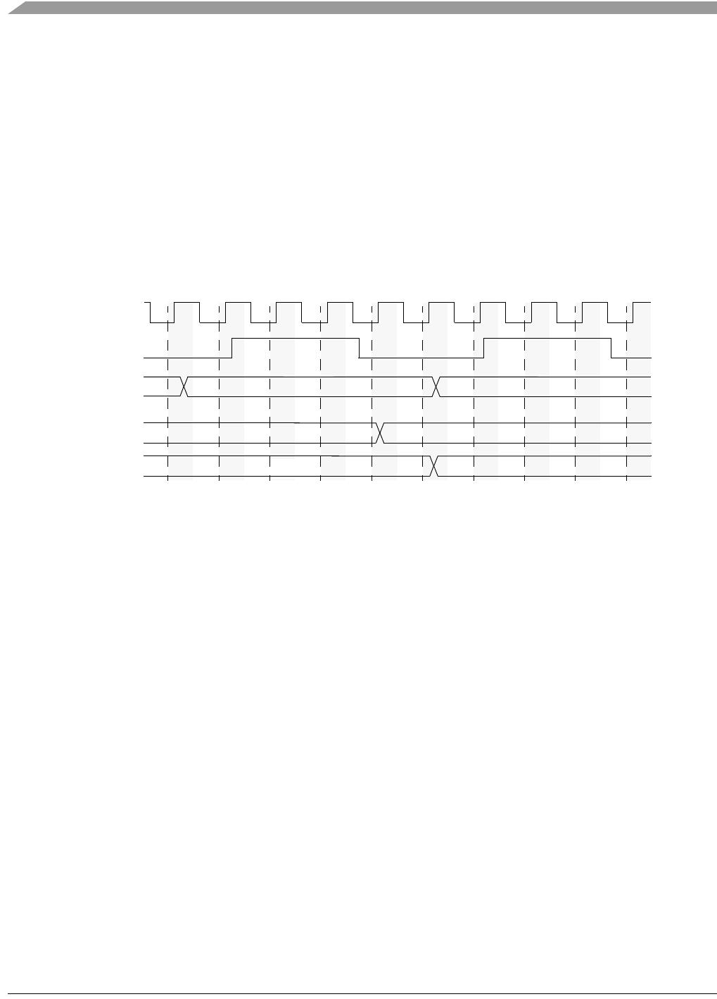
MCF548x Reference Manual, Rev. 3
8-30 Freescale Semiconductor
8.5.2 BDM Serial Interface
When the CPU is halted and PSTDDATA reflects the halt status, the development system can send
unrestricted commands to the debug module. The debug module implements a synchronous protocol using
two inputs (DSCLK and DSI) and one output (DSO), where DSO is specified as a delay relative to the
rising edge of the processor clock. See Table 8-1. The development system serves as the serial
communication channel master and must generate DSCLK.
The serial channel operates at a frequency from DC to 1/5 of the PSTCLK frequency. The channel uses
full-duplex mode, where data is sent and received simultaneously by both master and slave devices. The
transmission consists of 17-bit packets composed of a status/control bit and a 16-bit data word. As shown
in Figure 8-18, all state transitions are enabled on a rising edge of the PSTCLK clock when DSCLK is
high; that is, DSI is sampled and DSO is driven.
Figure 8-18. Maximum BDM Serial Interface Timing
DSCLK and DSI are synchronized inputs. DSCLK acts as a pseudo clock enable and is sampled, along
with DSI, on the rising edge of PSTCLK. DSO is delayed from the DSCLK-enabled PSTCLK rising edge
(registered after a BDM state machine state change). All events in the debug module’s serial state machine
are based on the PSTCLK rising edge. DSCLK must also be sampled low (on a positive edge of PSTCLK)
between each bit exchange. The msb is sent first. Because DSO changes state based on an internally
recognized rising edge of DSCLK, DSO cannot be used to indicate the start of a serial transfer. The
development system must count clock cycles in a given transfer. C0–C4 are described as follows:
• C0: Set the state of the DSI bit.
• C1: First synchronization cycle for DSI (DSCLK is high).
• C2: Second synchronization cycle for DSI (DSCLK is high).
• C3: BDM state machine changes state depending upon DSI and whether the entire input data
transfer has been transmitted.
• C4: DSO changes to next value.
NOTE
A not-ready response can be ignored except during a memory-referencing
cycle. Otherwise, the debug module can accept a new serial transfer after 32
processor clock periods.
8.5.2.1 Receive Packet Format
The basic receive packet, Figure 8-19, consists of 16 data bits and 1 status bit
PSTCLK
DSCLK
Next State
BDM State
Machine
DSO
DSI
Current State
Current Next
Past Current
C1 C2 C3 C4
C0

Background Debug Mode (BDM)
MCF548x Reference Manual, Rev. 3
Freescale Semiconductor 8-31
.
Table 8-22 describes receive BDM packet fields.
8.5.2.2 Transmit Packet Format
The basic transmit packet, Figure 8-20, consists of 16 data bits and 1 control bit.
Table 8-23 describes transmit BDM packet fields.
8.5.3 BDM Command Set
Table 8-24 summarizes the BDM command set. Subsequent paragraphs contain detailed descriptions of
each command. Issuing a BDM command when the processor is accessing debug module registers using
the WDEBUG instruction causes undefined behavior.
16 15 0
S Data Field [15:0]
Figure 8-19. Receive BDM Packet
Table 8-22. Receive BDM Packet Field Description
Bits Name Description
16 S Status. Indicates the status of CPU-generated messages listed below. The not-ready response can
be ignored unless a memory-referencing cycle is in progress. Otherwise, the debug module can
accept a new serial transfer after 32 processor clock periods.
S DataMessage
0 xxxx Valid data transfer
0 0xFFFFStatus OK
1 0x0000Not ready with response; come again
1 0x0001Error: Terminated bus cycle; data invalid
1 0xFFFFIllegal command
15–0 Data Data. Contains the message to be sent from the debug module to the development system. The
response message is always a single word, with the data field encoded as shown above.
16 15 0
CD[15:0]
Figure 8-20. Transmit BDM Packet
Table 8-23. Transmit BDM Packet Field Description
Bits Name Description
16 C Control. This bit is reserved. Command and data transfers initiated by the development
system should clear C.
15–0 Data Contains the data to be sent from the development system to the debug module.

MCF548x Reference Manual, Rev. 3
8-32 Freescale Semiconductor
Unassigned command opcodes are reserved by Freescale. All unused command formats within any
revision level perform a NOP and return the illegal command response.
Table 8-24. BDM Command Summary
Command Mnemonic Description CPU
State1
1General command effect and/or requirements on CPU operation:
- Halted. The CPU must be halted to perform this command.
- Steal. Command generates bus cycles that can be interleaved with bus accesses.
- Parallel. Command is executed in parallel with CPU activity.
Section Command
(Hex)
Read A/D
register
rareg/
rdreg
Read the selected address or data register and
return the results through the serial interface.
Halted 8.5.3.3.1 0x218 {A/D,
Reg[2:0]}
Write A/D
register
wareg/
wdreg
Write the data operand to the specified address or
data register.
Halted 8.5.3.3.2 0x208 {A/D,
Reg[2:0]}
Read
memory
location
read Read the data at the memory location specified by
the longword address.
Steal 8.5.3.3.3 0x1900—byte
0x1940—word
0x1980—lword
Write
memory
location
write Write the operand data to the memory location
specified by the longword address.
Steal 8.5.3.3.4 0x1800—byte
0x1840—word
0x1880—lword
Dump
memory
block
dump Used with READ to dump large blocks of memory. An
initial READ is executed to set up the starting address
of the block and to retrieve the first result. A DUMP
command retrieves subsequent operands.
Steal 8.5.3.3.5 0x1D00—byte
0x1D40—word
0x1D80—lword
Fill memory
block
fill Used with WRITE to fill large blocks of memory. An
initial WRITE is executed to set up the starting
address of the block and to supply the first operand.
A FILL command writes subsequent operands.
Steal 8.5.3.3.6 0x1C00—byte
0x1C40—word
0x1C80—lword
Resume
execution
go The pipeline is flushed and refilled before resuming
instruction execution at the current PC.
Halted 8.5.3.3.7 0x0C00
No operation nop Perform no operation; may be used as a null
command.
Parallel 8.5.3.3.8 0x0000
Output the
current PC
sync_pc Capture the current PC and display it on the
PSTDDATA output pins.
Parallel 8.5.3.3.9 0x0001
Read control
register
rcreg Read the system control register. Halted 8.5.3.3.11 0x2980
Write control
register
wcreg Write the operand data to the system control
register.
Halted 8.5.3.3.15 0x2880
Read debug
module
register
rdmreg Read the debug module register. Parallel 8.5.3.3.16 0x2D {0x42
DRc[4:0]}
20x4 is a three-bit field.
Write debug
module
register
wdmreg Write the operand data to the debug module
register.
Parallel 8.5.3.3.17 0x2C {0x42
DRc[4:0]}

Background Debug Mode (BDM)
MCF548x Reference Manual, Rev. 3
Freescale Semiconductor 8-33
8.5.3.1 ColdFire BDM Command Format
All ColdFire Family BDM commands include a 16-bit operation word followed by an optional set of one
or more extension words, as shown in Figure 8-21.
Table 8-25 describes BDM fields.
8.5.3.1.1 Extension Words as Required
Some commands require extension words for addresses or immediate data. Addresses require two
extension words because only absolute long addressing is permitted. Longword accesses are forcibly
longword-aligned and word accesses are forcibly word-aligned. Immediate data can be 1 or 2 words long.
Byte and word data each requires one extension word and longword data requires two extension words.
Operands and addresses are transferred most-significant word first. In the following descriptions of the
BDM command set, the optional set of extension words is defined as address, data, or operand data.
8.5.3.2 Command Sequence Diagrams
The command sequence diagram in Figure 8-22 shows serial bus traffic for commands. Each bubble
represents a 17-bit bus transfer. The top half of each bubble indicates the data the development system
15 1098765432 0
Operation 0 R/W Op Size 0 0 A/D Register
Extension Word(s)
Figure 8-21. BDM Command Format
Table 8-25. BDM Field Descriptions
Bit Name Description
15–10 Operation Specifies the command. These values are listed in Tabl e 8-24.
9—Reserved
8 R/W Direction of operand transfer.
0 Data is written to the CPU or to memory from the development system.
1 The transfer is from the CPU to the development system.
7–6 Operand
Size
Operand data size for sized operations. Addresses are expressed as 32-bit absolute
values. Note that a command performing a byte-sized memory read leaves the upper 8 bits
of the response data undefined. Referenced data is returned in the lower 8 bits of the
response.
Operand SizeBit Values
00 Byte8 bits
01 Word16 bits
10 Longword32 bits
11 Reserved—
5–4 — Reserved
3 A/D Address/data. Determines whether the register field specifies a data or address register.
0 Indicates a data register.
1 Indicates an address register.
2–0 Register Contains the register number in commands that operate on processor registers.
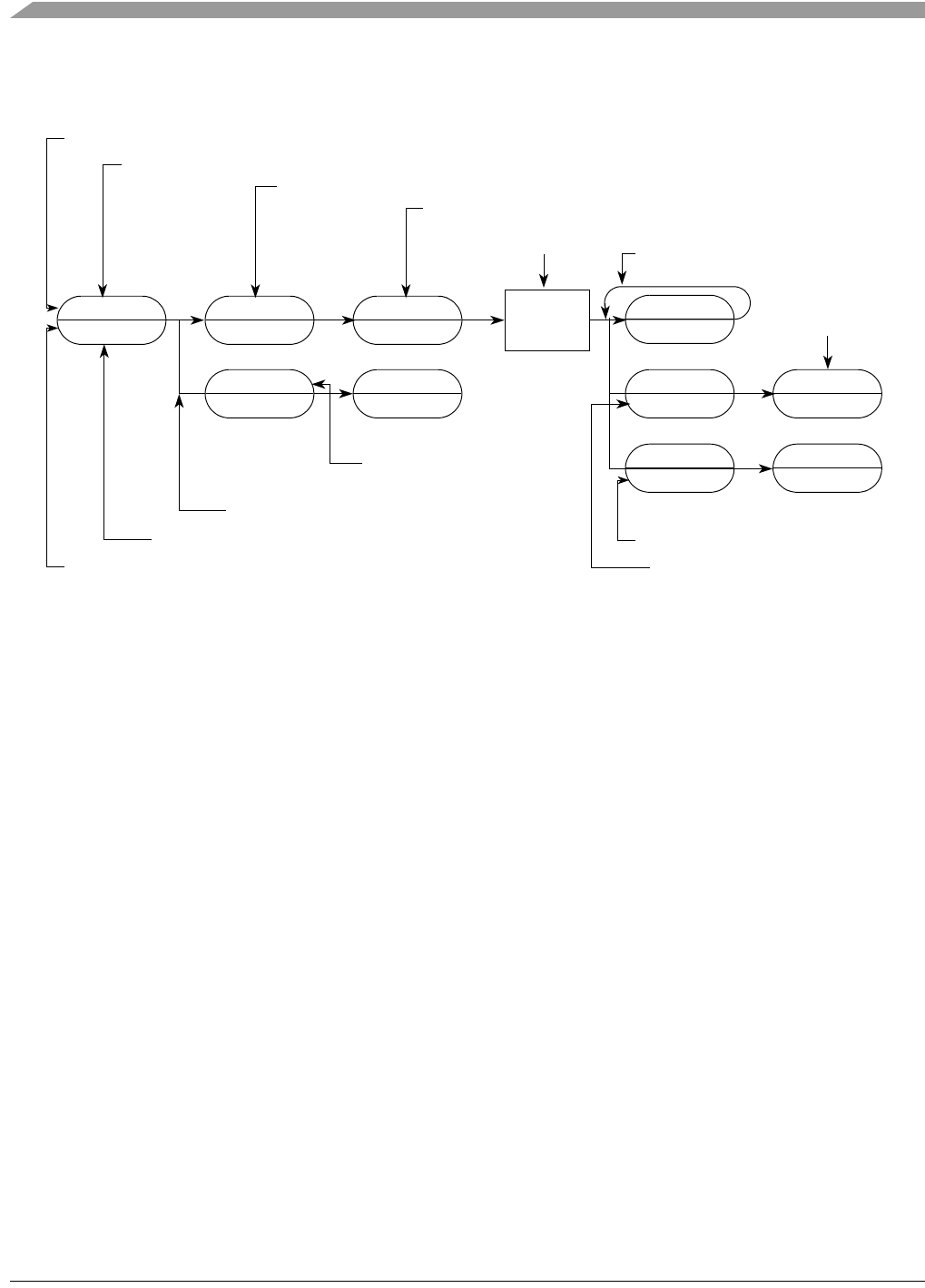
MCF548x Reference Manual, Rev. 3
8-34 Freescale Semiconductor
sends to the debug module; the bottom half indicates the debug module’s response to the previous
development system commands. Command and result transactions overlap to minimize latency.
Figure 8-22. Command Sequence Diagram
The sequence is as follows:
• In cycle 1, the development system command is issued (READ in this example). The debug module
responds with either the low-order results of the previous command or a command complete status
of the previous command, if no results are required.
• In cycle 2, the development system supplies the high-order 16 address bits. The debug module
returns a not-ready response unless the received command is decoded as unimplemented, which is
indicated by the illegal command encoding. If this occurs, the development system should
retransmit the command.
NOTE
A not-ready response can be ignored except during a memory-referencing
cycle. Otherwise, the debug module can accept a new serial transfer after 32
processor clock periods.
• In cycle 3, the development system supplies the low-order 16 address bits. The debug module
always returns a not-ready response.
• At the completion of cycle 3, the debug module initiates a memory read operation. Any serial
transfers that begin during a memory access return a not-ready response.
• Results are returned in the two serial transfer cycles after the memory access completes. For any
command performing a byte-sized memory read operation, the upper 8 bits of the response data are
undefined and the referenced data is returned in the lower 8 bits. The next command’s opcode is
sent to the debug module during the final transfer. If a memory or register access is terminated with
a bus error, the error status (S = 1, DATA = 0x0001) is returned instead of result data.
XXX
’NOT READY’
READ (LONG)
???
MS ADDR
’NOT READY’
LS ADDR
’NOT READY’
NEXT CMD
’NOT READY’
NEXT CMD
’NOT READY’
NEXT CMD
LS RESULT
Commands transmitted to the debug module
Command code transmitted during this cycle
High-order 16 bits of memory address
Low-order 16 bits of memory address
Non-serial-related
Next
Command
Code
Sequence taken if operation
has not completed
activity
READ
MEMORY
LOCATION
XXX
BERR
XXX
MS RESULT
XXX
’ILLEGAL’
Responses from the debug module
Results from previous command
Sequence taken if illegal command
is received by debug module
Data used from this transfer
Sequence taken if bus error
occurs on memory access
High- and low-order 16 bits of result
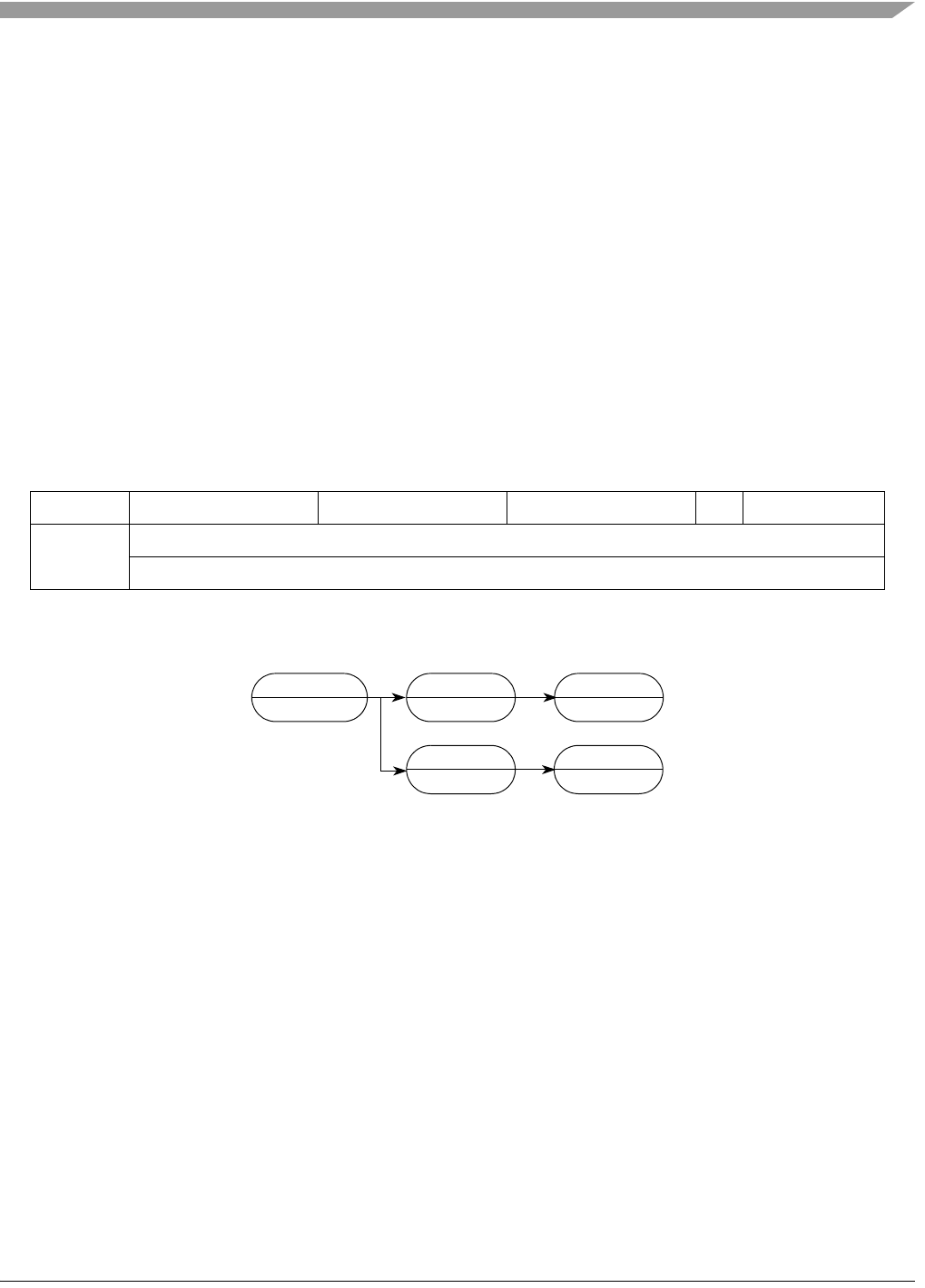
Background Debug Mode (BDM)
MCF548x Reference Manual, Rev. 3
Freescale Semiconductor 8-35
8.5.3.3 Command Set Descriptions
The following sections describe the commands summarized in Table 8-24.
NOTE
The BDM status bit (S) is 0 for normally completed commands. S = 1 for
illegal commands, not-ready responses, and transfers with bus-errors.
Section 8.5.2, “BDM Serial Interface,” describes the receive packet format.
Freescale reserves unassigned command opcodes for future expansion. Unused command formats in any
revision level perform a NOP and return an illegal command response.
8.5.3.3.1 Read A/D Register (RAREG/RDREG)
Read the selected address or data register and return the 32-bit result. A bus error response is returned if
the CPU core is not halted.
Command/Result Formats:
Command Sequence:
Figure 8-24. RAREG/RDREG Command Sequence
Operand Data: None
Result Data: The contents of the selected register are returned as a longword value,
most-significant word first.
8.5.3.3.2 Write A/D Register (WAREG/WDREG)
The operand longword data is written to the specified address or data register. A write alters all 32 register
bits. A bus error response is returned if the CPU core is not halted.
15 1211 87 432 0
Command 0x2 0x1 0x8 A/D Register
Result D[31:16]
D[15:0]
Figure 8-23. RAREG/RDREG Command Format
RAREG/RDREG
???
NEXT CMD
LS RESULT
NEXT CMD
’NOT READY’
XXX
BERR
XXX
MS RESULT
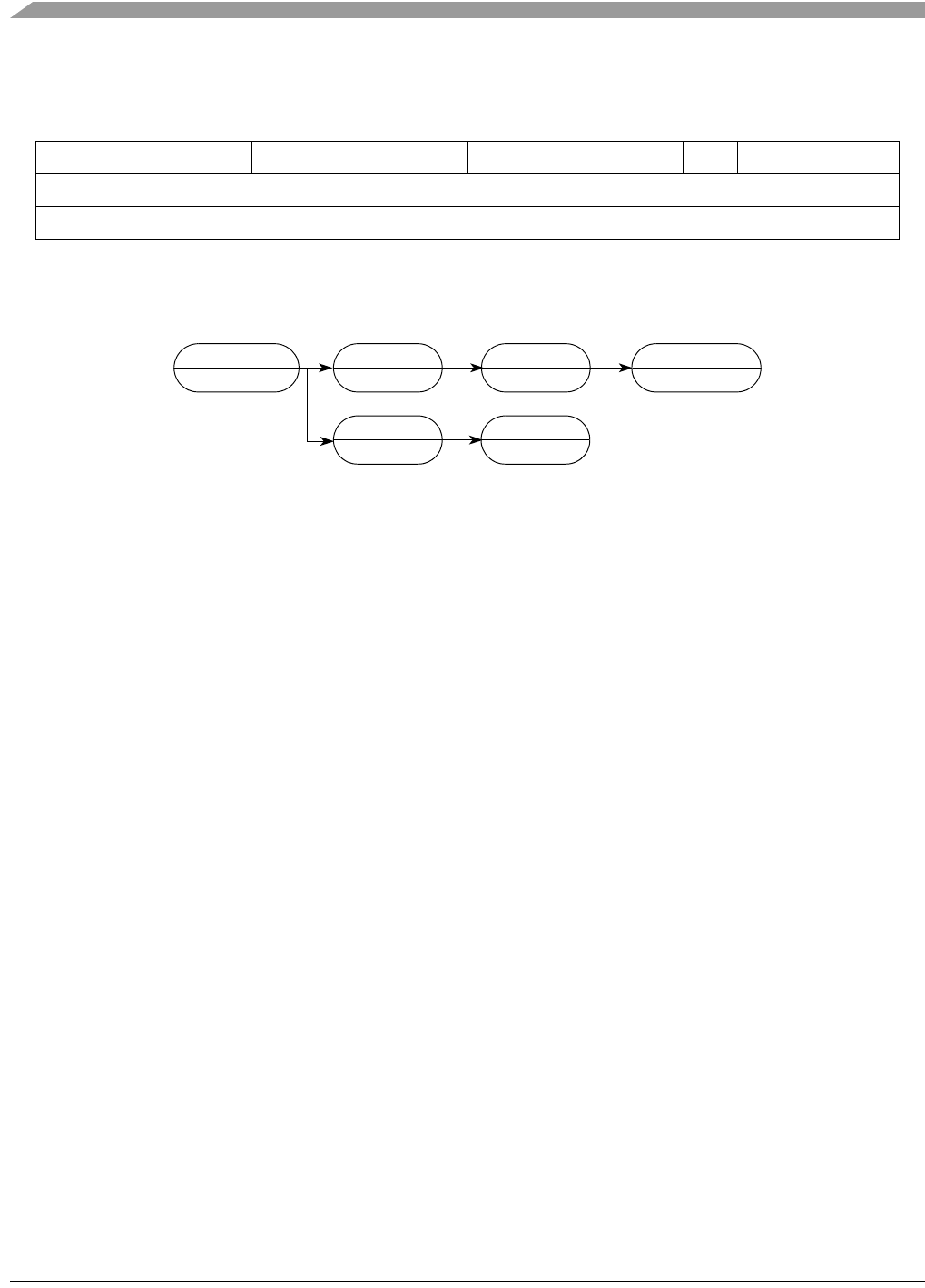
MCF548x Reference Manual, Rev. 3
8-36 Freescale Semiconductor
Command Format:
Command Sequence
Figure 8-26. WAREG/WDREG Command Sequence
Operand Data Longword data is written into the specified address or data register. The data is
supplied most-significant word first.
Result Data Command complete status is indicated by returning 0xFFFF (with S cleared)
when the register write is complete.
8.5.3.3.3 Read Memory Location (READ)
Read data at the longword address. Address space is defined by BAAR[TT,TM]. Hardware forces
low-order address bits to zeros for word and longword accesses to ensure that word addresses are
word-aligned and longword addresses are longword-aligned.
Command/Result Formats:
15 12 11 8 7 4 3 2 0
0x2 0x0 0x8 A/D Register
D[31:16]
D[15:0]
Figure 8-25. WAREG/WDREG Command Format
WAREG/WDREG
???
LS DATA
’NOT READY’
NEXT CMD
’NOT READY’
XXX
BERR
MS DATA
’NOT READY’
NEXT CMD
’CMD COMPLETE’
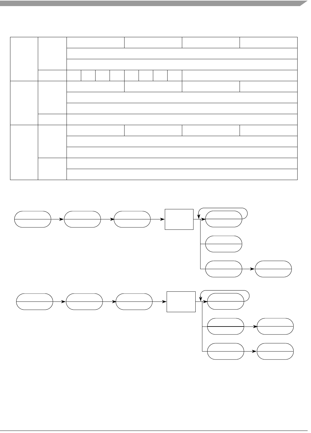
Background Debug Mode (BDM)
MCF548x Reference Manual, Rev. 3
Freescale Semiconductor 8-37
Command Sequence:
Figure 8-28. READ Command Sequence
Operand Data The only operand is the longword address of the requested location.
15 12 11 8 7 4 3 0
Byte
Command
0x1 0x9 0x0 0x0
A[31:16]
A[15:0]
ResultXXXXXXXX D[7:0]
Word Command 0x1 0x9 0x4 0x0
A[31:16]
A[15:0]
Result D[15:0]
Longword Command 0x1 0x9 0x8 0x0
A[31:16]
A[15:0]
Result D[31:16]
D[15:0]
Figure 8-27. READ Command/Result Formats
XXX
’NOT READY’
READ (LONG)
???
MS ADDR
’NOT READY’
LS ADDR
’NOT READY’
NEXT CMD
’NOT READY’
NEXT CMD
LS RESULT
READ
MEMORY
LOCATION
XXX
BERR
XXX
MS RESULT
XXX
’NOT READY’
READ (B/W)
???
MS ADDR
’NOT READY’
LS ADDR
’NOT READY’
NEXT CMD
’NOT READY’
READ
MEMORY
LOCATION
XXX
BERR
NEXT CMD
RESULT

MCF548x Reference Manual, Rev. 3
8-38 Freescale Semiconductor
Result Data Word results return 16 bits of data; longword results return 32. Bytes are returned
in the LSB of a word result, the upper byte is undefined. 0x0001 (S = 1) is returned
if a bus error occurs.
8.5.3.3.4 Write Memory Location (WRITE)
Write data to the memory location specified by the longword address. The address space is defined by
BAAR[TT,TM]. Hardware forces low-order address bits to zeros for word and longword accesses to
ensure that word addresses are word-aligned and longword addresses are longword-aligned.
Command Formats:
15 12 11 8 7 4 3 1
Byte 0x1 0x8 0x0 0x0
A[31:16]
A[15:0]
XXXXXXXX D[7:0]
Word 0x1 0x8 0x4 0x0
A[31:16]
A[15:0]
D[15:0]
Longword 0x1 0x8 0x8 0x0
A[31:16]
A[15:0]
D[31:16]
D[15:0]
Figure 8-29. WRITE Command Format
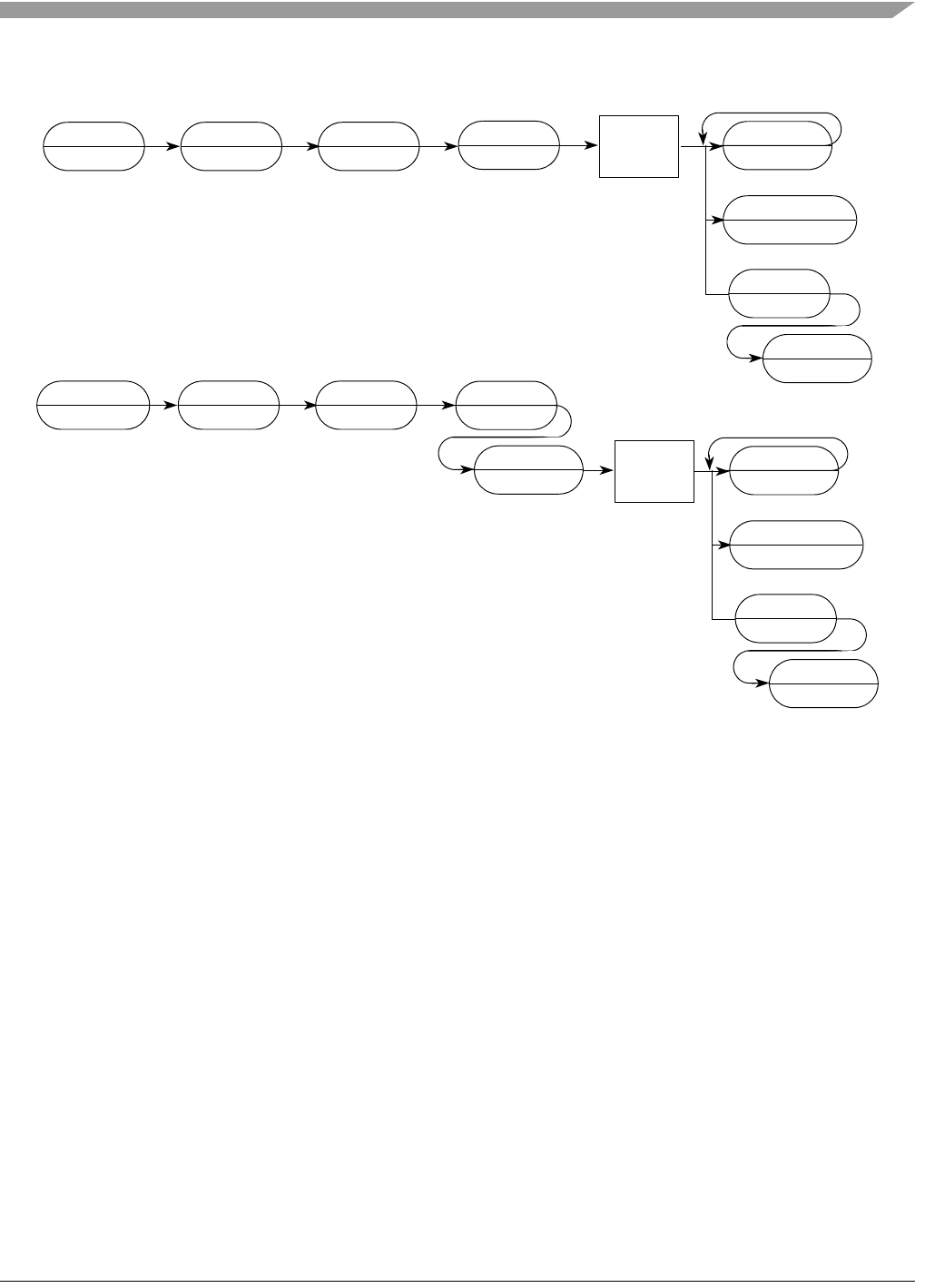
Background Debug Mode (BDM)
MCF548x Reference Manual, Rev. 3
Freescale Semiconductor 8-39
Command Sequence:
Figure 8-30. WRITE Command Sequence
Operand Data This two-operand instruction requires a longword absolute address that specifies
a location to which the data operand is to be written. Byte data is sent as a 16-bit
word, justified in the LSB; 16- and 32-bit operands are sent as 16 and 32 bits,
respectively.
Result Data Command complete status is indicated by returning 0xFFFF (with S cleared)
when the register write is complete. A value of 0x0001 (with S set) is returned if
a bus error occurs.
8.5.3.3.5 Dump Memory Block (DUMP)
DUMP is used with the READ command to access large blocks of memory. An initial READ is executed to
set up the starting address of the block and to retrieve the first result. If an initial READ is not executed
before the first DUMP, an illegal command response is returned. The DUMP command retrieves subsequent
operands. The initial address is incremented by the operand size (1, 2, or 4) and saved in a temporary
register. Subsequent DUMP commands use this address, perform the memory read, increment it by the
current operand size, and store the updated address in the temporary register.
XXX
’NOT READY’
WRITE (LONG)
???
MS ADDR
’NOT READY’
LS ADDR
’NOT READY’
WRITE
MEMORY
LOCATION
NEXT CMD
’CMD COMPLETE’
MS DATA
’NOT READY’
NEXT CMD
’NOT READY’
XXX
BERR
XXX
’NOT READY’
WRITE (B/W)
???
MS ADDR
’NOT READY’
LS ADDR
’NOT READY’
WRITE
MEMORY
LOCATION
NEXT CMD
’CMD COMPLETE’
DATA
’NOT READY’
NEXT CMD
’NOT READY’
XXX
BERR
LS DATA
’NOT READY’
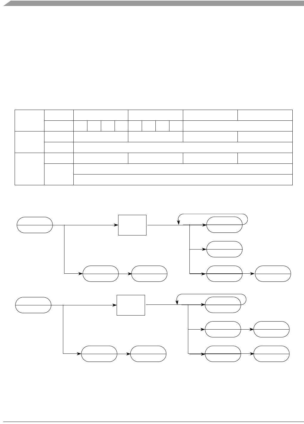
MCF548x Reference Manual, Rev. 3
8-40 Freescale Semiconductor
NOTE
DUMP does not check for a valid address; it is a valid command only when
preceded by NOP, READ, or another DUMP command. Otherwise, an illegal
command response is returned. NOP can be used for intercommand padding
without corrupting the address pointer.
The size field is examined each time a DUMP command is processed, allowing the operand size to be
dynamically altered.
Command/Result Formats:
Command Sequence:
Figure 8-32. DUMP Command Sequence
Operand Data: None
15 12 11 8 7 4 3 0
Byte Command 0x1 0xD 0x0 0x0
Result XXXXXXXX D[7:0]
Word Command 0x1 0xD 0x4 0x0
Result D[15:0]
Longword Command 0x1 0xD 0x8 0x0
Result D[31:16]
D[15:0]
Figure 8-31. DUMP Command/Result Formats
XXX
’NOT READY’
DUMP (B/W)
???
XXX
’ILLEGAL’
NEXT CMD
’NOT READY’
NEXT CMD
’NOT READY’
READ
MEMORY
LOCATION
XXX
BERR
NEXT CMD
RESULT
XXX
’NOT READY’
DUMP (LONG)
???
XXX
’ILLEGAL’
NEXT CMD
’NOT READY’
NEXT CMD
’NOT READY’
READ
MEMORY
LOCATION
XXX
BERR
NEXT CMD
MS RESULT
NEXT CMD
LS RESULT

Background Debug Mode (BDM)
MCF548x Reference Manual, Rev. 3
Freescale Semiconductor 8-41
Result Data: Requested data is returned as either a word or longword. Byte data is returned in
the least-significant byte of a word result. Word results return 16 bits of significant
data; longword results return 32 bits. A value of 0x0001 (with S set) is returned if
a bus error occurs.
8.5.3.3.6 Fill Memory Block (FILL)
A FILL command is used with the WRITE command to access large blocks of memory. An initial WRITE is
executed to set up the starting address of the block and to supply the first operand. The FILL command
writes subsequent operands. The initial address is incremented by the operand size (1, 2, or 4) and saved
in a temporary register after the memory write. Subsequent FILL commands use this address, perform the
write, increment it by the current operand size, and store the updated address in the temporary register.
If an initial WRITE is not executed preceding the first FILL command, the illegal command response is
returned.
NOTE
The FILL command does not check for a valid address: FILL is a valid
command only when preceded by another FILL, a NOP, or a WRITE command.
Otherwise, an illegal command response is returned. The NOP command can
be used for intercommand padding without corrupting the address pointer.
The size field is examined each time a FILL command is processed, allowing the operand size to be altered
dynamically.
Command Formats:
15 12 11 8 7 4 3 0
Byte 0x1 0xC 0x0 0x0
XXXXXXXX D[7:0]
Word 0x1 0xC 0x4 0x0
D[15:0]
Longword 0x1 0xC 0x8 0x0
D[31:16]
D[15:0]
Figure 8-33. FILL Command Format
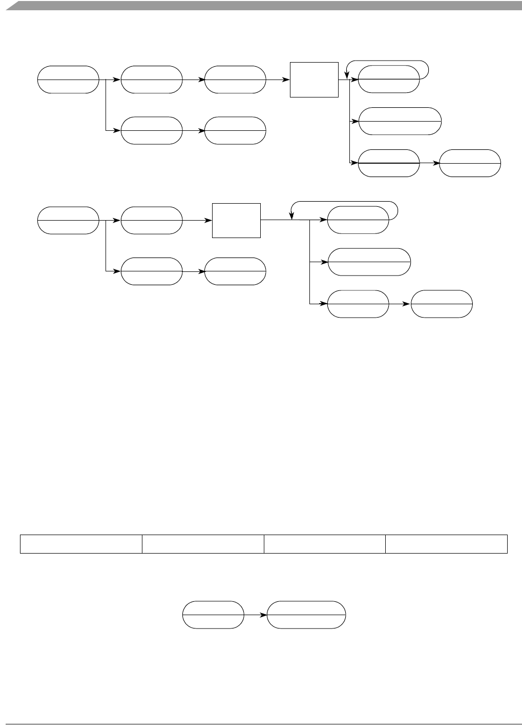
MCF548x Reference Manual, Rev. 3
8-42 Freescale Semiconductor
Command Sequence:
Figure 8-34. FILL Command Sequence
Operand Data: A single operand is data to be written to the memory location. Byte data is sent as
a 16-bit word, justified in the least-significant byte; 16- and 32-bit operands are
sent as 16 and 32 bits, respectively.
Result Data: Command complete status (0xFFFF) is returned when the register write is
complete. A value of 0x0001 (with S set) is returned if a bus error occurs.
8.5.3.3.7 Resume Execution (GO)
The pipeline is flushed and refilled before normal instruction execution resumes. Prefetching begins at the
current address in the PC and at the current privilege level. If any register (such as the PC or SR) is altered
by a BDM command while the processor is halted, the updated value is used when prefetching resumes.
If a GO command is issued and the CPU is not halted, the command is ignored.
Command Sequence:
Figure 8-36. GO Command Sequence
Operand Data: None
15 12 11 8 7 4 3 0
0x0 0xC 0x0 0x0
Figure 8-35. GO Command Format
XXX
’NOT READY’
FILL (B/W)
???
DATA
’NOT READY’
NEXT CMD
’NOT READY’
WRITE
MEMORY
LOCATION
XXX
BERR
NEXT CMD
’CMD COMPLETE’
XXX
’ILLEGAL’
NEXT CMD
’NOT READY’
XXX
’NOT READY’
FILL (LONG)
???
MS DATA
’NOT READY’
LS DATA
’NOT READY’
WRITE
MEMORY
LOCATION
XXX
BERR
NEXT CMD
’CMD COMPLETE’
XXX
’ILLEGAL’
NEXT CMD
’NOT READY’
NEXT CMD
’NOT READY’
GO
???
NEXT CMD
’CMD COMPLETE’

Background Debug Mode (BDM)
MCF548x Reference Manual, Rev. 3
Freescale Semiconductor 8-43
Result Data: The command-complete response (0xFFFF) is returned during the next shift
operation.
8.5.3.3.8 No Operation (NOP)
NOP performs no operation and may be used as a null command where required.
Command Formats:
Command Sequence:
Figure 8-38. NOP Command Sequence
Operand Data: None
Result Data: The command-complete response, 0xFFFF (with S cleared), is returned during the
next shift operation.
8.5.3.3.9 Synchronize PC to the PSTDDATA Lines (SYNC_PC)
The SYNC_PC command captures the current PC and displays it on the PSTDDATA outputs. After the
debug module receives the command, it sends a signal to the ColdFire processor that the current PC must
be displayed. The processor then forces an instruction fetch at the next PC with the address being captured
in the DDATA logic under control of CSR[BTB]. The specific sequence of PSTDDATA values is as
follows:
1. Debug signals a SYNC_PC command is pending.
2. CPU completes the current instruction.
3. CPU forces an instruction fetch to the next PC, generates a PST = 0x5 value indicating a taken
branch and signals the capture of DDATA.
4. The instruction address corresponding to the PC is captured.
5. The PST marker (0x9–0xB) is generated and displayed as defined by CSR[BTB] followed by the
captured PC address.
If the option to display ASID is enabled (CSR[3] = 1), the 8-bit ASID follows the address. That is, the
PSTDDATA sequence is {0x5, Marker, Instruction Address, 0x8, ASID}, where the 0x8 is the marker for
the ASID.
The SYNC_PC command can be used to dynamically access the PC for performance monitoring. The
execution of this command is considerably less obtrusive to the real-time operation of an application than
a HALT-CPU/READ-PC/RESUME command sequence.
Command Formats:
15 12 11 8 7 4 3 0
0x00x00x00x0
Figure 8-37. NOP Command Format
NOP
???
NEXT CMD
’CMD COMPLETE’

MCF548x Reference Manual, Rev. 3
8-44 Freescale Semiconductor
Command Sequence:
Figure 8-40. SYNC_PC Command Sequence
Operand Data: None
Result Data: Command complete status (0xFFFF) is returned when the register write is
complete.
8.5.3.3.10 Force Transfer Acknowledge (FORCE_TA)
DEBUG_D logic implements the new FORCE_TA serial BDM command to resolve a hung bus condition.
In some system designs, references to certain unmapped memory addresses may cause the external bus to
hang with no transfer acknowledge generated by any bus responders. The FORCE_TA forces generation of
a transfer acknowledge signal, which can be logically summed into the normal acknowledge logic located
in the system integration module (SIM) outside of the ColdFire core.
There are two scenarios of interest, one caused by a processor access and the other caused by a BDM
access. The following sequences identify the operations needed to break the hung bus condition:
• Bus hang caused by processor or external or internal alternate master:
— Assert the breakpoint input to force a processor core halt.
— If the bus hang was caused by a processor access, send in FORCE_TA commands until the
processor is halted, as signaled by PST = 0xF. Due to pipeline and store buffer depths, many
memory accesses may be queued up behind the access causing the bus hang. Repeated
FORCE_TA commands eventually allow processing of all these pending accesses. As soon as the
processor is halted, the system reaches a quiescent, controllable state.
— If the hang was caused by another master, such as a DMA channel, the processor can halt
immediately. In this case as well, multiple assertions of the FORCE_TA command may be
required to terminate the alternate master’s errant access.
• Bus hang caused by BDM access:
— It is assumed the processor is already halted at the time of the errant BDM access. To resolve
the hung bus, it is necessary to process four or more FORCE_TA commands, because the BDM
command may have initiated a cache line access that fetches 4 longwords, each needing a
unique transfer acknowledge.
Formats:
Command Sequence:
15 12 11 8 7 4 3 0
0x00x00x00x1
Figure 8-39. SYNC_PC Command Format
15 12 11 8 7 4 3 0
0x00x00x00x2
Figure 8-41. FORCE_TA Command
SYNC_PC
???
NEXT CMD
“CMD COMPLETE”
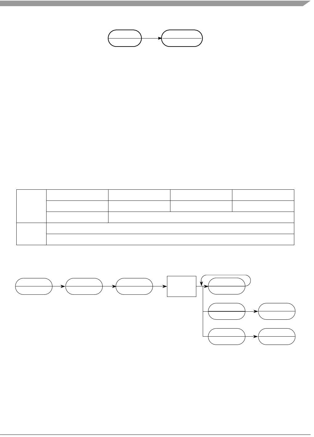
Background Debug Mode (BDM)
MCF548x Reference Manual, Rev. 3
Freescale Semiconductor 8-45
Figure 8-42. FORCE_TA Command Sequence
Operand Data: None
Result Data: The command complete response, 0xFFFF (with the status bit cleared), is returned
during the next shift operation. This response indicates the FORCE_TA command
was processed correctly and does not necessarily reflect the status of any internal
bus.
8.5.3.3.11 Read Control Register (RCREG)
Read the selected control register and return the 32-bit result. Accesses to the processor/memory control
registers are always 32 bits wide, regardless of register width. The second and third words of the command
form a 32-bit address, which the debug module uses to generate a special bus cycle to access the specified
control register. The 12-bit Rc field is the same as that used by the MOVEC instruction.
Command/Result Formats:
Command Sequence:
Figure 8-44. RCREG Command Sequence
Operand Data: The only operand is the 32-bit Rc control register select field.
Result Data: Control register contents are returned as a longword, most-significant word first.
The implemented portion of registers smaller than 32 bits is guaranteed correct;
other bits are undefined.
Rc encoding: See Table 8-26.
15 12 11 8 7 4 3 0
Command 0x2 0x9 0x8 0x0
0x0 0x0 0x0 0x0
0x0 Rc
Result D[31:16]
D[15:0]
Figure 8-43. RCREG Command/Result Formats
FORCE_TA
???
NEXT CMD
“CMD COMPLETE”
XXX
’NOT READY’
RCREG
???
MS ADDR
’NOT READY’
MS ADDR
’NOT READY’
NEXT CMD
’NOT READY’
READ
CONTROL
REGISTER
XXX
BERR
NEXT CMD
MS RESULT
NEXT CMD
LS RESULT

MCF548x Reference Manual, Rev. 3
8-46 Freescale Semiconductor
Table 8-26. ColdFire CPU Control Register Map
Name CPU Space (Rc) Register Name
Memory Management Control Registers
CACR 0x002 Cache control register
ASID 0x003 Address space identifier
ACR0–ACR3 0x004–0x007 Access control registers 0–3
MMUBAR 0x008 MMU base address register
Processor General-Purpose Registers
D0–D7 0x(0,1)80–0x(0,1)87 Data registers 0–7 (0 = load, 1 = store)
A0–A7 0x(0,1)88–0x(0,1)8F Address registers 0–7 (0 = load, 1 = store) A7 is user stack pointer
Processor Miscellaneous Registers
OTHER_A7 0x800 Other stack pointer
VBR 0x801 Vector base register
MACSR 0x804 MAC status register
MASK 0x805 MAC address mask register
ACC0–ACC3 0x806–0x80B MAC accumulators 0–3
ACCext01 0x807 MAC accumulator 0, 1 extension bytes
ACCext23 0x808 MAC accumulator 2, 3 extension bytes
SR 0x80E Status register
PC 0x80F Program counter
Processor Floating-Point Registers
FPU0 0x810 32 msbs of floating-point data register 0
FPL0 0x811 32 lsbs of floating-point data register 0
FPU1 0x812 32 msbs of floating-point data register 1
FPL1 0x813 32 lsbs of floating-point data register 1
FPU2 0x814 32 msbs of floating-point data register 2
FPL2 0x815 32 lsbs of floating-point data register 2
FPU3 0x816 32 msbs of floating-point data register 3
FPL3 0x817 32 lsbs of floating-point data register 3
FPU4 0x818 32 msbs of floating-point data register 4
FPL4 0x819 32 lsbs of floating-point data register 4
FPU5 0x81A 32 msbs of floating-point data register 5
FPL5 0x81B 32 lsbs of floating-point data register 5
FPU6 0x81C 32 msbs of floating-point data register 6

Background Debug Mode (BDM)
MCF548x Reference Manual, Rev. 3
Freescale Semiconductor 8-47
8.5.3.3.12 BDM Accesses of the Stack Pointer Registers (A7: SSP and USP)
The Version 4 ColdFire core supports two unique stack pointer (A7) registers: the supervisor stack pointer
(SSP) and the user stack pointer (USP). The hardware implementation of these two programmable-visible
32-bit registers does not uniquely identify one as the SSP and the other as the USP. Rather, the hardware
uses one 32-bit register as the currently-active A7; the other is named simply the OTHER_A7. Thus, the
contents of the two hardware registers is a function of the operating mode of the processor:
if SR[S] = 1
then A7 = Supervisor Stack Pointer
OTHER_A7 = User Stack Pointer
else A7 = User Stack Pointer
OTHER_A7 = Supervisor Stack Pointer
The BDM programming model supports reads and writes to A7 and OTHER_A7 directly. It is the
responsibility of the external development system to determine the mapping of A7 and OTHER_A7 to the
two program-visible definitions (supervisor and user stack pointers), based on the SR[S].
8.5.3.3.13 BDM Accesses of the EMAC Registers
The presence of rounding logic in the output datapath of the EMAC requires special care for
BDM-initiated reads and writes of its programming model. In particular, any result rounding modes must
be disabled during the read/write process so the exact bit-wise EMAC register contents are accessed.
For example, a BDM read of an accumulator (ACCx) requires the following sequence:
BdmReadACCx (
rcreg macsr; // read current macsr contents & save
wcreg #0,macsr; // disable all rounding modes
rcreg ACCx; // read the desired accumulator
wcreg #saved_data,macsr; // restore the original macsr
)
FPL6 0x81D 32 lsbs of floating-point data register 6
FPU7 0x81E 32 msbs of floating-point data register 7
FPL7 0x81F 32 lsbs of floating-point data register 7
FPIAR 0x821 Floating-point instruction address register
FPSR 0x822 Floating-point status register
FPCR 0x824 Floating-point control register
Local Memory and Module Control Registers
RAMBAR0 0xC04 RAM base address register 0
RAMBAR1 0xC05 RAM base address register 1
MBAR 0xC0F Primary module base address register (not a core register)
Table 8-26. ColdFire CPU Control Register Map (Continued)
Name CPU Space (Rc) Register Name

MCF548x Reference Manual, Rev. 3
8-48 Freescale Semiconductor
Likewise, to write an accumulator register, the following BDM sequence is needed:
BdmWriteACCx (
rcreg macsr; // read current macsr contents & save
wcreg #0,macsr; // disable all rounding modes
wcreg #data,ACCx; // write the desired accumulator
wcreg #saved_data,macsr; // restore the original macsr
)
Additionally, writes to the accumulator extension registers must be performed after the corresponding
accumulators are updated because a write to any accumulator alters the corresponding extension register
contents.
For more information on saving and restoring the complete EMAC programming model, see the
appropriate section of the EMAC chapter.
8.5.3.3.14 BDM Accesses of Floating-Point Data Registers (FPn)
The ColdFire debug architecture allows BDM accesses of the entire programming model (including all
FPU-related registers) of the processor core using RCREG and WCREG. However, certain hardware
restrictions require the accesses related to the 64-bit FPn data registers be performed in a certain manner
to guarantee correct operation.
The serial BDM command structure supports 8-, 16- and 32-bit accesses, but there is no direct mechanism
for accessing 64-bit data values. Rather than changing this well-established protocol and command set,
BDM accesses of 64-bit data values are treated as two independent 32-bit references. In particular, 64-bit
FPn data registers are treated as two separate values from the BDM perspective. Each FPn is partitioned
into upper and lower longwords, FPUn and FPLn.
Either longword can be read first. The processor treats the BDM read command as a pseudo-FMOVEM.
Accordingly, all rounding modes and exception enables are ignored and the 32-bit contents of FPUn or
FPLn are sent to the debug module for transmission over the serial communication channel. The FPU
programming model is unchanged.
To write to an FPU data register, FPUn must be written first and followed by a write to FPLn. The
processor operates as follows: the BDM write to FPUn is performed, which loads the upper 32 bits of an
internal double-precision operand register; the BDM write to FPLn loads the supplied operand into the
lower 32 bits of the same internal register, and the entire 64-bit value is loaded into the selected FPn.
Failure to execute this sequence of commands produces an undefined value in the FPUn.
Note that any BDM write of an FPU register changes the internal state from NULL to IDLE.
8.5.3.3.15 Write Control Register (WCREG)
The operand (longword) data is written to the specified control register. The write alters all 32 register bits.
See the RCREG instruction description for the Rc encoding and for additional notes on writes to the A7
stack pointers and the EMAC and FPU programming models.
Command/Result Formats:
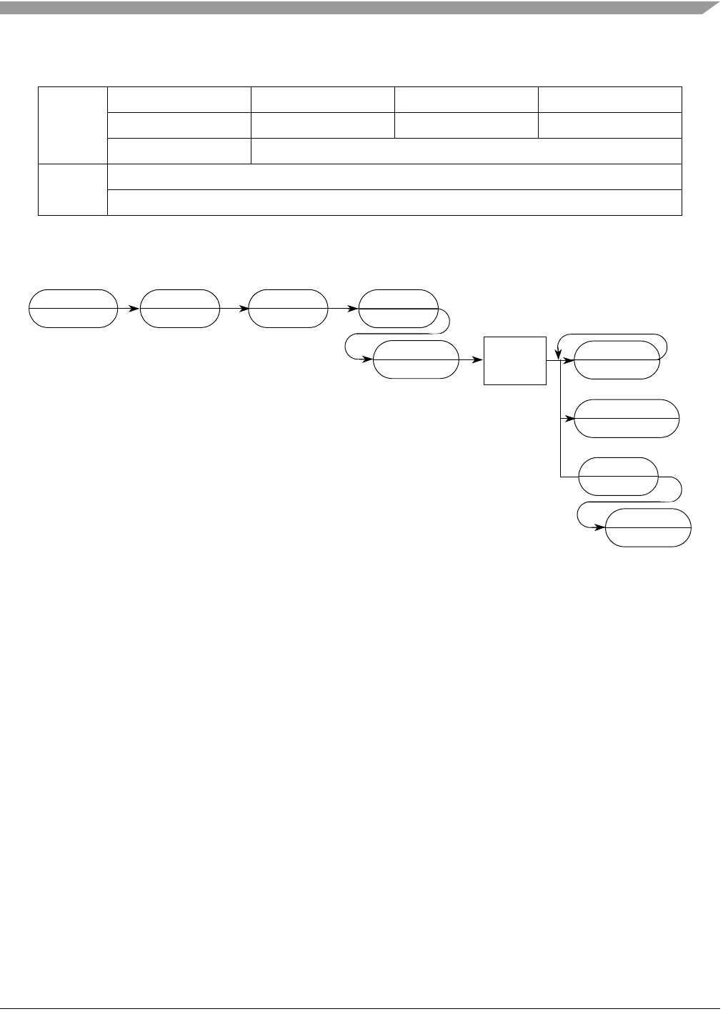
Background Debug Mode (BDM)
MCF548x Reference Manual, Rev. 3
Freescale Semiconductor 8-49
Command Sequence:
Figure 8-46. WCREG Command Sequence
Operand Data: This instruction requires two longword operands. The first selects the register to
which the operand data is to be written; the second contains the data.
Result Data: Successful write operations return 0xFFFF. Bus errors on the write cycle are
indicated by the setting of bit 16 in the status message and by a data pattern of
0x0001.
8.5.3.3.16 Read Debug Module Register (RDMREG)
Read the selected debug module register and return the 32-bit result. The only valid register selection for
the RDMREG command is CSR (DRc = 0x00). Note that this read of the CSR clears the trigger status bits
(CSR[BSTAT]) if either a level-2 breakpoint has been triggered or a level-1 breakpoint has been triggered
and no level-2 breakpoint has been enabled.
Command/Result Formats:
15 12 11 8 7 4 3 0
Command 0x2 0x8 0x8 0x0
0x0 0x0 0x0 0x0
0x0 Rc
Result D[31:16]
D[15:0]
Figure 8-45. WCREG Command/Result Formats
XXX
’NOT READY’
WCREG
???
MS ADDR
’NOT READY’
MS ADDR
’NOT READY’
WRITE
CONTROL
REGISTER
NEXT CMD
’CMD COMPLETE’
MS DATA
’NOT READY’
NEXT CMD
’NOT READY’
XXX
BERR
LS DATA
’NOT READY’
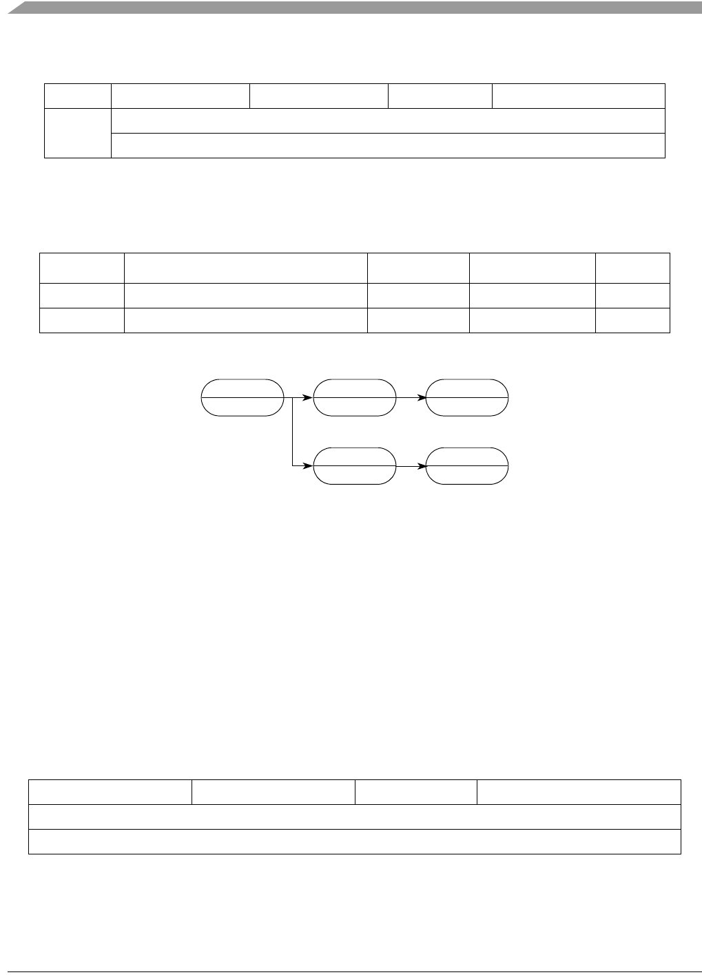
MCF548x Reference Manual, Rev. 3
8-50 Freescale Semiconductor
Table 8-27 shows the definition of DRc encoding.
Command Sequence:
Figure 8-48. RDMREG Command Sequence
Operand Data: None
Result Data: The contents of the selected debug register are returned as a longword value. The
data is returned most-significant word first.
8.5.3.3.17 Write Debug Module Register (WDMREG)
The operand (longword) data is written to the specified debug module register. All 32 bits of the register
are altered by the write. DSCLK must be inactive while the debug module register writes from the CPU
accesses are performed using the WDEBUG instruction.
Command Format:
Table 8-6 shows the definition of the DRc write encoding.
Command Sequence:
15 12 11 8 7 5 4 0
Command 0x2 0xD 100 DRc
Result D[31:16]
D[15:0]
Figure 8-47. RDMREG BDM Command/Result Formats
Table 8-27. Definition of DRc Encoding—Read
DRc[4:0] Debug Register Definition Mnemonic Initial State Page
0x00 Configuration/Status CSR 0x0 p. 8-11
0x01–0x1F Reserved — — —
Figure 8-49. WDMREG BDM Command Format
15 12 11 8 7 5 4 0
0x2 0xC 100 DRc
D[31:16]
D[15:0]
RDMREG
???
XXX
MS RESULT
NEXT CMD
LS RESULT
XXX
’ILLEGAL’
NEXT CMD
’NOT READY’

Real-Time Debug Support
MCF548x Reference Manual, Rev. 3
Freescale Semiconductor 8-51
Figure 8-50. WDMREG Command Sequence
Operand Data: Longword data is written into the specified debug register. The data is supplied
most-significant word first.
Result Data: Command complete status (0xFFFF) is returned when register write is complete.
8.6 Real-Time Debug Support
The ColdFire Family provides support debugging real-time applications. For these types of embedded
systems, the processor must continue to operate during debug. The foundation of this area of debug support
is that while the processor cannot be halted to allow debugging, the system can generally tolerate the small
intrusions of the BDM inserting instructions into the pipeline with minimal effect on real-time operation.
The debug module provides three types of breakpoints: PC with mask, operand address range, and data
with mask. These breakpoints can be configured into one- or two-level triggers with the exact trigger
response also programmable. The debug module programming model can be written from either the
external development system using the debug serial interface or from the processor’s supervisor
programming model using the WDEBUG instruction. Only CSR is readable using the external
development system.
8.6.1 Theory of Operation
Breakpoint hardware can be configured through TDR[TCR] to respond to triggers by displaying
PSTDDATA, initiating a processor halt, or generating a debug interrupt. As shown in Table 8-28, when a
breakpoint is triggered, an indication (CSR[BSTAT]) is provided on the PSTDDATA output port of the
DDATA information when it is not displaying captured processor status, operands, or branch addresses.
See Section 8.3.2, “Processor Stopped or Breakpoint State Change (PST = 0xE).”
The breakpoint status is also posted in CSR. Note that CSR[BSTAT] is cleared by a CSR read when either
a level-2 breakpoint is triggered or a level-1 breakpoint is triggered and a level-2 breakpoint is not enabled.
Status is also cleared by writing to either TDR or XTDR to disable trigger options.
Table 8-28. PSTDDATA Nibble/CSR[BSTAT] Breakpoint Response
PSTDDATA Nibble/CSR[BSTAT] 1
1Encodings not shown are reserved for future use.
Breakpoint Status
0000/0000 No breakpoints enabled
0010/0001 Waiting for level-1 breakpoint
0100/0010 Level-1 breakpoint triggered
1010/0101 Waiting for level-2 breakpoint
1100/0110 Level-2 breakpoint triggered
WDMREG
???
MS DATA
’NOT READY’
LS DATA
’NOT READY’
XXX
’ILLEGAL’
NEXT CMD
’NOT READY’
NEXT CMD
’CMD COMPLETE’

MCF548x Reference Manual, Rev. 3
8-52 Freescale Semiconductor
BDM instructions use the appropriate registers to load and configure breakpoints. As the system operates,
a breakpoint trigger generates the response defined in TDR.
PC breakpoints are treated in a precise manner: exception recognition and processing are initiated before
the excepting instruction is executed. All other breakpoint events are recognized on the processor’s local
bus, but are made pending to the processor and sampled like other interrupt conditions. As a result, these
interrupts are said to be imprecise.
In systems that tolerate the processor being halted, a BDM-entry can be used. With TDR[TRC] =01, a
breakpoint trigger causes the core to halt (PST = 0xF).
If the processor core cannot be halted, the debug interrupt can be used. With this configuration,
TDR[TRC] = 10, the breakpoint trigger becomes a debug interrupt to the processor, which is treated higher
than the nonmaskable level-7 interrupt request. As with all interrupts, it is made pending until the
processor reaches a sample point, which occurs once per instruction. Again, the hardware forces the PC
breakpoint to occur before the targeted instruction executes and is precise. This is possible because the PC
breakpoint is enabled when interrupt sampling occurs. For address and data breakpoints, reporting is
considered imprecise because several instructions may execute after the triggering address or data is
detected.
As soon as the debug interrupt is recognized, the processor aborts execution and initiates exception
processing. This event is signaled externally by the assertion of a unique PST value (PST = 0xD) for
multiple cycles. The core enters emulator mode when exception processing begins. After the standard
8-byte exception stack is created, the processor fetches a unique exception vector from the vector table.
Table 8-29 describes the two unique entries that distinguish PC breakpoints from other trigger events.
(Refer to the ColdFire Programmer’s Reference Manual.)
In the case of a two-level trigger, the last breakpoint event determines the exception vector; however, if
the second-level trigger is PC || Address {&& Data} (as shown in the last condition in the code example
in Section 8.4.11.1, “Resulting Set of Possible Trigger Combinations”), the vector taken is determined by
the first condition that occurs after the first-level trigger: vector 13 if PC occurs first or vector 12 if Address
{&& Data} occurs first. If both occur simultaneously, the non-PC-breakpoint debug interrupt is taken
(vector number 12).
Execution continues at the instruction address in the vector corresponding to the breakpoint triggered. The
debug interrupt handler can use supervisor instructions to save the necessary context such as the state of
all program-visible registers into a reserved memory area.
During a debug interrupt service routine, all normal interrupt requests are evaluated and sampled once per
instruction. If any exception occurs, the processor responds as follows:
1. It saves a copy of the current value of the emulator mode state bit and then exits emulator mode by
clearing the actual state.
2. Bit 1 of the fault status field (FS1) in the next exception stack frame is set to indicate the
processor was in emulator mode when the interrupt occurred. This corresponds to bit 17 of the
longword at the top of the system stack. See Section 3.8.1, “Exception Stack Frame Definition.”
3. It passes control to the appropriate exception handler.
Table 8-29. Exception Vector Assignments
Vector Number Vector Offset (Hex) Stacked Program Counter Assignment
12 0x030 Next Non-PC-breakpoint debug interrupt
13 0x034 Next PC-breakpoint debug interrupt

Real-Time Debug Support
MCF548x Reference Manual, Rev. 3
Freescale Semiconductor 8-53
4. It executes an RTE instruction when the exception handler finishes. During the processing of the
RTE, FS1 is reloaded from the system stack. If this bit is set, the processor sets the emulator mode
state and resumes execution of the original debug interrupt service routine. This is signaled
externally by the generation of the PST value that originally identified the debug interrupt
exception, that is, PST = 0xD.
Fault status encodings are listed in Table 5-2. Implementation of this debug interrupt handling fully
supports the servicing of a number of normal interrupt requests during a debug interrupt service routine.
The emulator mode state bit is essentially changed to be a program-visible value, stored into memory
during exception stack frame creation, and loaded from memory by the RTE instruction.
When debug interrupt operations complete, the RTE instruction executes and the processor exits emulator
mode. After the debug interrupt handler completes execution, the external development system can use
BDM commands to read the reserved memory locations.
In Revision A, if a hardware breakpoint such as a PC trigger is left unmodified by the debug interrupt
service routine, another debug interrupt is generated after the completion of the RTE instruction. In
Revisions B and C, the generation of another debug interrupt during the first instruction after the RTE exits
emulator mode is inhibited. This behavior is consistent with the existing logic involving trace mode where
the first instruction executes before another trace exception is generated. Thus, all hardware breakpoints
are disabled until the first instruction after the RTE completes execution, regardless of the programmed
trigger response.
8.6.1.1 Emulator Mode
Emulator mode is used to facilitate nonintrusive emulator functionality. This mode can be entered in three
different ways:
• Setting CSR[EMU] forces the processor into emulator mode. EMU is examined only if RSTI is
negated and the processor begins reset exception processing. It can be set while the processor is
halted before reset exception processing begins. See Section 8.5.1, “CPU Halt.”
• A debug interrupt always puts the processor in emulation mode when debug interrupt exception
processing begins.
• Setting CSR[TRC] forces the processor into emulation mode when trace exception processing
begins.
While operating in emulation mode, the processor exhibits the following properties:
• Unmasked interrupt requests are serviced. The resulting interrupt exception stack frame has FS[1]
set to indicate the interrupt occurred while in emulator mode.
• If CSR[MAP] = 1, all caching of memory and the SRAM module are disabled. All memory
accesses are forced into a specially mapped address space signaled by TT = 0x2, TM = 0x5 or 0x6.
This includes stack frame writes and the vector fetch for the exception that forced entry into this
mode.
The RTE instruction exits emulation mode. The processor status output port provides a unique encoding
for emulator mode entry (0xD) and exit (0x7).
8.6.2 Concurrent BDM and Processor Operation
The debug module supports concurrent operation of both the processor and most BDM commands. BDM
commands may be executed while the processor is running, except the following:
• Read/write address and data registers

MCF548x Reference Manual, Rev. 3
8-54 Freescale Semiconductor
• Read/write control registers
For BDM commands that access memory, the debug module requests the processor’s local bus. The
processor responds by stalling the instruction fetch pipeline and waiting for current bus activity to
complete before freeing the local bus for the debug module to perform its access. After the debug module
bus cycle, the processor reclaims the bus.
NOTE
Breakpoint registers must be carefully configured in a development system
if the processor is executing. The debug module contains no hardware
interlocks, so TDR and XTDR should be disabled while breakpoint registers
are loaded, after which TDR and XTDR can be written to define the exact
trigger. This prevents spurious breakpoint triggers.
Because there are no hardware interlocks in the debug unit, no BDM operations are allowed while the CPU
is writing the debug’s registers (DSCLK must be inactive).
8.7 Debug C Definition of PSTDDATA Outputs
This section specifies the ColdFire processor and debug module’s generation of the PSTDDATA output on
an instruction basis. In general, the PSTDDATA output for an instruction is defined as follows:
PSTDDATA = 0x1, {[0x89B], operand}
where the {...} definition is optional operand information defined by the setting of the CSR.
The CSR provides capabilities to display operands based on reference type (read, write, or both). A PST
value {0x8, 0x9, or 0xB} identifies the size and presence of valid data to follow on the PSTDDATA output
{1, 2, or 4 bytes}. Additionally, for certain change-of-flow branch instructions, CSR[BTB] provides the
capability to display the target instruction address on the PSTDDATA output {2, 3, or 4 bytes} using a PST
value of {0x9, 0xA, or 0xB}.
8.7.1 User Instruction Set
Table 8-30 shows the PSTDDATA specification for user-mode instructions. Rn represents any {Dn, An}
register. In this definition, the ‘y’ suffix generally denotes the source and ‘x’ denotes the destination
operand. For a given instruction, the optional operand data is displayed only for those effective addresses
referencing memory.
Table 8-30. PSTDDATA Specification for User-Mode Instructions
Instruction Operand Syntax PSTDDATA
add.l <ea>y,Dx PSTDDATA = 0x1,{0xB, source operand}
add.l Dy,<ea>x PSTDDATA = 0x1,{0xB, source},{0xB, destination}
adda.l <ea>y,Ax PSTDDATA = 0x1,{0xB, source operand}
addi.l #<data>,Dx PSTDDATA = 0x1
addq.l #<data>,<ea>x PSTDDATA = 0x1,{0xB, source},{0xB, destination}
addx.l Dy,Dx PSTDDATA = 0x1
and.l <ea>y,Dx PSTDDATA = 0x1,{0xB, source operand}
and.l Dy,<ea>x PSTDDATA = 0x1,{0xB, source},{0xB, destination}

Debug C Definition of PSTDDATA Outputs
MCF548x Reference Manual, Rev. 3
Freescale Semiconductor 8-55
andi.l #<data>,Dx PSTDDATA = 0x1
asl.l {Dy,#<data>},Dx PSTDDATA = 0x1
asr.l {Dy,#<data>},Dx PSTDDATA = 0x1
bcc.{b,w,l} if taken, then PSTDDATA = 0x5, else PSTDDATA = 0x1
bchg.{b,l} #<data>,<ea>x PSTDDATA = 0x1,{0x8, source},{0x8, destination}
bchg.{b,l} Dy,<ea>x PSTDDATA = 0x1,{0x8, source},{0x8, destination}
bclr.{b,l} #<data>,<ea>x PSTDDATA = 0x1,{0x8, source},{0x8, destination}
bclr.{b,l} Dy,<ea>x PSTDDATA = 0x1,{0x8, source},{0x8, destination}
bra.{b,w,l} PSTDDATA = 0x5
bset.{b,l} #<data>,<ea>x PSTDDATA = 0x1,{0x8, source},{0x8, destination}
bset.{b,l} Dy,<ea>x PSTDDATA = 0x1,{0x8, source},{0x8, destination}
bsr.{b,w,l} PSTDDATA = 0x5,{0xB, destination operand}
btst.{b,l} #<data>,<ea>x PSTDDATA = 0x1,{0x8, source operand}
btst.{b,l} Dy,<ea>x PSTDDATA = 0x1,{0x8, source operand}
clr.b <ea>x PSTDDATA = 0x1,{0x8, destination operand}
clr.l <ea>x PSTDDATA = 0x1,{0xB, destination operand}
clr.w <ea>x PSTDDATA = 0x1,{0x9, destination operand}
cmp.b <ea>y,Dx PSTDDATA = 0x1, {0x8, source operand}
cmp.l <ea>y,Dx PSTDDATA = 0x1,{0xB, source operand}
cmp.w <ea>y,Dx PSTDDATA = 0x1, {0x9, source operand}
cmpa.l <ea>y,Ax PSTDDATA = 0x1,{0xB, source operand}
cmpa.w <ea>y,Ax PSTDDATA = 0x1, {0x9, source operand}
cmpi.b #<data>,Dx PSTDDATA = 0x1
cmpi.l #<data>,Dx PSTDDATA = 0x1
cmpi.w #<data>,Dx PSTDDATA = 0x1
divs.l <ea>y,Dx PSTDDATA = 0x1,{0xB, source operand}
divs.w <ea>y,Dx PSTDDATA = 0x1,{0x9, source operand}
divu.l <ea>y,Dx PSTDDATA = 0x1,{0xB, source operand}
divu.w <ea>y,Dx PSTDDATA = 0x1,{0x9, source operand}
eor.l Dy,<ea>x PSTDDATA = 0x1,{0xB, source},{0xB, destination}
eori.l #<data>,Dx PSTDDATA = 0x1
ext.l Dx PSTDDATA = 0x1
ext.w Dx PSTDDATA = 0x1
Table 8-30. PSTDDATA Specification for User-Mode Instructions (Continued)
Instruction Operand Syntax PSTDDATA

MCF548x Reference Manual, Rev. 3
8-56 Freescale Semiconductor
extb.l Dx PSTDDATA = 0x1
illegal PSTDDATA = 0x11
jmp <ea>y PSTDDATA = 0x5, {[0x9AB], target address} 2
jsr <ea>y PSTDDATA = 0x5, {[0x9AB], target address},{0xB , destination operand}2
lea.l <ea>y,Ax PSTDDATA = 0x1
link.w Ay,#<displacement> PSTDDATA = 0x1,{0xB, destination operand}
lsl.l {Dy,#<data>},Dx PSTDDATA = 0x1
lsr.l {Dy,#<data>},Dx PSTDDATA = 0x1
mov3q.l #<data>,<ea>x PSTDDATA = 0x1, {0xB, destination operand}
move.b <ea>y,<ea>x PSTDDATA = 0x1,{0x8, source},{0x8, destination}
move.l <ea>y,<ea>x PSTDDATA = 0x1,{0xB, source},{0xB, destination}
move.w <ea>y,<ea>x PSTDDATA = 0x1,{0x9, source},{0x9, destination}
move.w CCR,Dx PSTDDATA = 0x1
move.w {Dy,#<data>},CCR PSTDDATA = 0x1
movea.l <ea>y,Ax PSTDDATA = 0x1,{0xB, source}
movea.w <ea>y,Ax PSTDDATA = 0x1,{0x9, source}
movem.l #list,<ea>x PSTDDATA = 0x1,{0xB, destination},... 3
movem.l <ea>y,#list PSTDDATA = 0x1,{0xB, source},... 3
moveq.l #<data>,Dx PSTDDATA = 0x1
muls.l <ea>y,Dx PSTDDATA = 0x1,{0xB, source operand}
muls.w <ea>y,Dx PSTDDATA = 0x1,{0x9, source operand}
mulu.l <ea>y,Dx PSTDDATA = 0x1,{0xB, source operand}
mulu.w <ea>y,Dx PSTDDATA = 0x1,{0x9, source operand}
mvs.b <ea>y,Dx PSTDDATA = 0x1, {0x8, source operand}
mvs.w <ea>y,Dx PSTDDATA = 0x1, {0x9, source operand}
mvz.b <ea>y,Dx PSTDDATA = 0x1, {0x8, source operand}
mvz.w <ea>y,Dx PSTDDATA = 0x1, {0x9, source operand}
neg.l Dx PSTDDATA = 0x1
negx.l Dx PSTDDATA = 0x1
nop PSTDDATA = 0x1
not.l Dx PSTDDATA = 0x1
or.l <ea>y,Dx PSTDDATA = 0x1,{0xB, source operand}
or.l Dy,<ea>x PSTDDATA = 0x1,{0xB, source},{0xB, destination}
Table 8-30. PSTDDATA Specification for User-Mode Instructions (Continued)
Instruction Operand Syntax PSTDDATA

Debug C Definition of PSTDDATA Outputs
MCF548x Reference Manual, Rev. 3
Freescale Semiconductor 8-57
ori.l #<data>,Dx PSTDDATA = 0x1
pea.l <ea>y PSTDDATA = 0x1,{0xB, destination operand}
pulse PSTDDATA = 0x4
rems.l <ea>y,Dw:Dx PSTDDATA = 0x1,{0xB, source operand}
remu.l <ea>y,Dw:Dx PSTDDATA = 0x1,{0xB, source operand}
rts PSTDDATA = 0x1, PSTDDATA = 0x5, {[0x9AB], target address}
sats.l Dx PSTDDATA = 0x1
scc.b Dx PSTDDATA = 0x1
sub.l <ea>y,Dx PSTDDATA = 0x1,{0xB, source operand}
sub.l Dy,<ea>x PSTDDATA = 0x1,{0xB, source},{0xB, destination}
suba.l <ea>y,Ax PSTDDATA = 0x1,{0xB, source operand}
subi.l #<data>,Dx PSTDDATA = 0x1
subq.l #<data>,<ea>x PSTDDATA = 0x1,{0xB, source},{0xB, destination}
subx.l Dy,Dx PSTDDATA = 0x1
swap.w Dx PSTDDATA = 0x1
tas.b <ea>x PSTDDATA = 0x1, {0x8, source}, {0x8, destination}
tpf PST = 0x1
tpf.l #<data> PST = 0x1
tpf.w #<data> PST = 0x1
trap #<data> PSTDDATA = 0x11
tst.b <ea>x PSTDDATA = 0x1,{0x8, source operand}
tst.l <ea>y PSTDDATA = 0x1,{0xB, source operand}
tst.w <ea>y PSTDDATA = 0x1,{0x9, source operand}
unlk Ax PSTDDATA = 0x1,{0xB, destination operand}
wddata.b <ea>y PSTDDATA = 0x4, {0x8, source operand
wddata.l <ea>y PSTDDATA = 0x4, {0xB, source operand
wddata.w <ea>y PSTDDATA = 0x4, {0x9, source operand
Table 8-30. PSTDDATA Specification for User-Mode Instructions (Continued)
Instruction Operand Syntax PSTDDATA

MCF548x Reference Manual, Rev. 3
8-58 Freescale Semiconductor
Table 8-31 shows the PSTDDATA specification for multiply-accumulate instructions.
1During normal exception processing, the PSTDDATA output is driven to a 0xC indicating the exception
processing state. The exception stack write operands, as well as the vector read and target address of the
exception handler may also be displayed.
Exception ProcessingPSTDDATA = 0xC,{0xB,destination},// stack frame
{0xB,destination},// stack frame
{0xB,source},// vector read
PSTDDATA = 0x5,{[0x9AB],target}// handler PC
The PSTDDATA specification for the reset exception is shown below:
Exception ProcessingPSTDDATA = 0xC,
PSTDDATA = 0x5,{[0x9AB],target}// handler PC
The initial references at address 0 and 4 are never captured nor displayed since these accesses are treated
as instruction fetches.
For all types of exception processing, the PSTDDATA = 0xC value is driven at all times, unless the PSTDDATA
output is needed for one of the optional marker values or for the taken branch indicator (0x5).
2For JMP and JSR instructions, the optional target instruction address is displayed only for those effective
address fields defining variant addressing modes. This includes the following <ea>x values: (An), (d16,An),
(d8,An,Xi), (d8,PC,Xi).
3For Move Multiple instructions (MOVEM), the processor automatically generates line-sized transfers if the
operand address reaches a 0-modulo-16 boundary and there are four or more registers to be transferred. For
these line-sized transfers, the operand data is never captured nor displayed, regardless of the CSR value.
The automatic line-sized burst transfers are provided to maximize performance during these sequential
memory access operations.
Table 8-31. PSTDDATA Values for User-Mode Multiply-Accumulate Instructions
Instruction Operand Syntax PSTDDATA
mac.l Ry,Rx PSTDDATA = 0x1
mac.l Ry,Rx,<ea>y,Rw,ACCx PSTDDATA = 0x1,{0xB, source operand}
mac.l Ry,Rx,ACCx PSTDDATA = 0x1
mac.l Ry,Rx,ea,Rw PSTDDATA = 0x1,{0xB, source operand}
mac.w Ry,Rx PSTDDATA = 0x1
mac.w Ry,Rx,<ea>y,Rw,ACCx PSTDDATA = 0x1,{0xB, source operand}
mac.w Ry,Rx,ACCx PSTDDATA = 0x1
mac.w Ry,Rx,ea,Rw PSTDDATA = 0x1,{0xB, source operand}
move.l {Ry,#<data>},ACCext01 PSTDDATA = 0x1
move.l {Ry,#<data>},ACCext23 PSTDDATA = 0x1
move.l {Ry,#<data>},ACCx PSTDDATA = 0x1
move.l {Ry,#<data>},MACSR PSTDDATA = 0x1
move.l {Ry,#<data>},MASK PSTDDATA = 0x1
move.l ACCext01,Rx PSTDDATA = 0x1
move.l ACCext23,Rx PSTDDATA = 0x1
move.l ACCy,ACCx PSTDDATA = 0x1

Debug C Definition of PSTDDATA Outputs
MCF548x Reference Manual, Rev. 3
Freescale Semiconductor 8-59
Table 8-32 shows the PSTDDATA specification for floating-point instructions; note that <ea>y includes
FPy, Dy, Ay, and <mem>y addressing modes. The optional operand capture and display applies only to the
<mem>y addressing modes. Note also that the PSTDDATA values are the same for a given instruction,
regardless of explicit rounding precision.
move.l ACCy,Rx PSTDDATA = 0x1
move.l MACSR,CCR PSTDDATA = 0x1
move.l MACSR,Rx PSTDDATA = 0x1
move.l MASK,Rx PSTDDATA = 0x1
msac.l Ry,Rx PSTDDATA = 0x1
msac.l Ry,Rx,<ea>y,Rw,ACCx PSTDDATA = 0x1,{0xB, source operand}
msac.l Ry,Rx,ACCx PSTDDATA = 0x1
msac.l Ry,Rx,<ea>y,Rw PSTDDATA = 0x1,{0xB, source},{0xB, destination}
msac.w Ry,Rx PSTDDATA = 0x1
msac.w Ry,Rx,<ea>y,Rw,ACCx PSTDDATA = 0x1,{0xB, source operand}
msac.w Ry,Rx,ACCx PSTDDATA = 0x1
msac.w Ry,Rx,<ea>y,Rw PSTDDATA = 0x1,{0xB, source},{0xB, destination}
Table 8-32. PSTDDATA Values for User-Mode Floating-Point Instructions
Instruction 1Operand Syntax PSTDDATA
fabs.sz <ea>y,FPx PSTDDATA = 0x1, [89B], source}
fadd.sz <ea>y,FPx PSTDDATA = 0x1, [89B], source}
fbcc.{w,l} <label> if taken, then PSTDDATA = 5, else PSTDDATA = 0x1
fcmp.sz <ea>y,FPx PSTDDATA = 0x1, [89B], source}
fdiv.sz <ea>y,FPx PSTDDATA = 0x1, [89B], source}
fint.sz <ea>y,FPx PSTDDATA = 0x1, [89B], source}
fintrz.sz <ea>y,FPx PSTDDATA = 0x1, [89B], source}
fmove.sz <ea>y,FPx PSTDDATA = 0x1, [89B], source}
fmove.sz FPy,<ea>x PSTDDATA = 0x1, [89B], destination}
fmove.l <ea>y,FP*R PSTDDATA = 0x1, B, source}
fmove.l FP*R,<ea>x PSTDDATA = 0x1, B, destination}
fmovem <ea>y,#list PSTDDATA = 0x1
fmovem #list,<ea>x PSTDDATA = 0x1
fmul.sz <ea>y,FPx PSTDDATA = 0x1, [89B], source}
Table 8-31. PSTDDATA Values for User-Mode Multiply-Accumulate Instructions (Continued)
Instruction Operand Syntax PSTDDATA

MCF548x Reference Manual, Rev. 3
8-60 Freescale Semiconductor
Depending on the size of any external memory operand specified by the f<op>.fmt field, the data marker
is defined as shown in Table 8-33.
8.7.2 Supervisor Instruction Set
The supervisor instruction set has complete access to the user mode instructions plus the opcodes shown
below. The PSTDDATA specification for these opcodes is shown in Table 8-34.
fneg.sz <ea>y,FPx PSTDDATA = 0x1, [89B], source}
fnop PSTDDATA = 0x1
fsqrt.sz <ea>y,FPx PSTDDATA = 0x1, [89B], source}
fsub.sz <ea>y,FPx PSTDDATA = 0x1, [89B], source}
ftst.sz <ea>y PSTDDATA = 0x1, [89B], source}
1The FP*R notation refers to the floating-point control registers: FPCR, FPSR, and FPIAR.
Table 8-33. Data Markers and FPU Operand Format Specifiers
Format Specifier Data Marker
.b 8
.w 9
.l B
.s B
.d Never captured
Table 8-34. PSTDDATA Specification for Supervisor-Mode Instructions
Instruction Operand Syntax PSTDDATA
cpushl dc,(Ax)
ic,(Ax)
bc,(Ax)
PSTDDATA = 0x1
frestore <ea>y PSTDDATA = 0x1
fsave <ea>x PSTDDATA = 0x1
halt PSTDDATA = 0x1,
PSTDDATA = 0xF
intouch (Ay) PSTDDATA = 0x1
move.l Ay,USP PSTDDATA = 0x1
move.l USP,Ax PSTDDATA = 0x1
move.w SR,Dx PSTDDATA = 0x1
move.w {Dy,#<data>},SR PSTDDATA = 0x1, {0x3}
Table 8-32. PSTDDATA Values for User-Mode Floating-Point Instructions (Continued)
Instruction 1Operand Syntax PSTDDATA

ColdFire Debug History
MCF548x Reference Manual, Rev. 3
Freescale Semiconductor 8-61
The move-to-SR and RTE instructions include an optional PSTDDATA = 0x3 value, indicating an entry
into user mode. Additionally, if the execution of a RTE instruction returns the processor to emulator mode,
a multiple-cycle status of 0xD is signaled.
Similar to the exception processing mode, the stopped state (PSTDDATA = 0xE) and the halted state
(PSTDDATA = 0xF) display this status throughout the entire time the ColdFire processor is in the given
mode.
8.8 ColdFire Debug History
This section describes the origins of the ColdFire debug systems.
8.8.1 ColdFire Debug Classic: The Original Definition
The original design, Revision A, provided debug support in three separate areas:
• Real-time trace
• Background debug mode (BDM)
• Real-time debug
The real-time debug features may be accessed from the external BDM emulator or from the supervisor
programming model of the processor. The hardware breakpoint registers include: a PC breakpoint + mask,
two address registers for defining a specific address or a range of addresses, and a data breakpoint + mask.
The original design supported breakpoints of the form:
if PC_breakpoint is triggered
then respond using user-defined configuration
if Address_breakpoint {&& Data_breakpoint} is triggered
then respond using user-defined configuration
Two-level triggers of the form:
if PC_breakpoint is triggered
then if Address_breakpoint {&& Data_breakpoint} is triggered
then respond using user-defined configuration
if Address_breakpoint {&& Data_breakpoint} is triggered
then if PC_breakpoint is triggered
then respond using user-defined configuration
movec.l Ry,Rc PSTDDATA = 0x1, {8, ASID}
rte PSTDDATA = 0x7, {0xB, source operand}, {3}, {0xB, source operand}, {DD},
PSTDDATA = 0x5, {[0x9AB], target address}
stop #<data> PSTDDATA = 0x1,
PSTDDATA = 0xE
wdebug.l <ea>y PSTDDATA = 0x1, {0xB, source, 0xB, source}
Table 8-34. PSTDDATA Specification for Supervisor-Mode Instructions (Continued)
Instruction Operand Syntax PSTDDATA

MCF548x Reference Manual, Rev. 3
8-62 Freescale Semiconductor
The data_breakpoint can be included as an optional part of an address breakpoint.
The ColdFire debug architecture was created to provide this set of functionality without requiring the
traditional connection to the external system bus. Rather, the functionality is provided using only a
connection to a Freescale-defined 26-pin debug connector. By providing the required debug signals in
customer-specific designs, standard third-party emulators can be used for debug of these designs.
NOTE
The baseline debug functionality is described in any of the ColdFire
MCF52xx User’s Manuals, which are available as PDF files at:
http://www.freescale.com/ColdFire/. As an example, see the debug section
of the MCF5272 User’s Manual located under MCF5272 Product
Information.
8.8.2 ColdFire Debug Revision B
During development of the Version 3 ColdFire design, there were a number of enhancements to the
original debug functionality requested by customers and third-party developers. These requests resulted in
an expanded set of debug functionality named Revision B.
The Rev. B enhancements are as follows:
• Addition of a BDM SYNC_PC command to display the processor’s current PC
• Creation of more flexible hardware breakpoint triggers, i.e., support for “OR” combinations
• Removal of the restrictions involving concurrent hardware breakpoint use and BDM command
activity
• Redefinition of the processor status values for the RTS instruction
• An external mechanism to generate a debug interrupt
• A mechanism to inhibit debug interrupts after the RTE exit
• A mechanism to identify the revision level of the debug module
Rev. B enhancements provide backward compatibility with the original design.
8.8.3 ColdFire Debug Revision C
Continuing discussions with customers and the developer community led to Revision C design
enhancements primarily related to improvements in the real-time debug capabilities of the ColdFire
architecture. The remainder of this section details these enhancements.
8.8.3.1 Debug Interrupts and Interrupt Requests (Emulator Mode)
In Rev. A and Rev. B ColdFire debug implementations, the response to a user-defined breakpoint trigger
can be configured to be one of three possibilities:
• The breakpoint trigger can merely be displayed on the DDATA bus, with no internal reaction to the
trigger. The trigger state information is displayed on DDATA in all situations.
• The breakpoint trigger can force the processor to halt and allow BDM activities.
• The breakpoint trigger can generate a special debug interrupt to allow real-time systems to quickly
process the interrupt and return to normal system executing as rapidly as possible.
The occurrence of the debug interrupt exception is treated as a special type of interrupt. It is considered to
be higher in priority than all normal interrupt requests and has special processor status values to provide
an external indication that this interrupt has occurred.

Freescale-Recommended BDM Pinout
MCF548x Reference Manual, Rev. 3
Freescale Semiconductor 8-63
Additionally, the execution of the debug interrupt service routine is forced to be interrupt-inhibited by the
processor hardware. While in this service routine, there is an optional capability to map all instruction and
operand references into a separate address space, so that an emulator could define the routine dynamically.
The current processor implementations actually include a program-invisible state bit that defines this
emulator mode of operation. Also note, the interrupt mask level is not modified during the processing of
a debug interrupt.
Customers with real-time embedded systems have specifically asked for the ability to service normal
interrupt requests while processing the debug interrupt service routine. In many systems of this type,
motion-based servo interrupts must be considered as the highest priority interrupt request.
To provide this functionality and be able to service any number of normal interrupt requests (including the
possibility of nested interrupts), the processor state signaling emulator mode must be included as part of
the exception stack frame.
As part of the Rev. C functionality, the operation of the debug interrupt is modified in the following
manner:
1. The occurrence of the breakpoint trigger, configured to generate a debug interrupt, is treated
exactly as before. The debug interrupt is treated as a higher priority exception relative to the normal
interrupt requests encoded on the interrupt priority input signals.
2. At the appropriate sample point, the ColdFire processor initiates debug interrupt exception
processing. This event is signaled externally by the generation of a unique PST value (PST =
0xD) asserted for multiple cycles. The processor sets the emulator mode state bit as part of this
exception processing.
3. While the processor in the debug interrupt service routine, all normal interrupt requests are
evaluated and sampled once per instruction. While in this routine, if any type of exception occurs,
the processor responds in the following manner:
a) In response to the new exception, the processor saves a copy of the current value of the
emulator mode state bit and then exits emulator mode by clearing the actual state.
b) The new exception stack frame sets bit 1 of the fault status field, using the saved emulator
mode bit, indicating execution while in emulator mode has been interrupted. This corresponds
to bit 17 of the longword at the top of the system stack.
c) Control is passed to the appropriate exception handler.
d) When the exception handler is complete, a Return From Exception (RTE) instruction is
executed. During the processing of the RTE, FS[1] is reloaded from the system stack. If this
bit is asserted, the processor sets the emulator mode state and resumes execution of the
original debug interrupt service routine. This is signaled externally by the generation of the
PST value that originally identified the occurrence of a debug interrupt exception, that is,
PST = 0xD.
Implementation of this revised debug interrupt handling fully supports the servicing of any number of
normal interrupt requests while in a debug interrupt service routine. The emulator mode state bit is
essentially changed to be a program-visible value, stored into memory during exception stack frame
creation and loaded from memory by the RTE instruction.
8.9 Freescale-Recommended BDM Pinout
The ColdFire BDM connector, Figure 8-51, is a 26-pin Berg connector arranged 2 x 13.
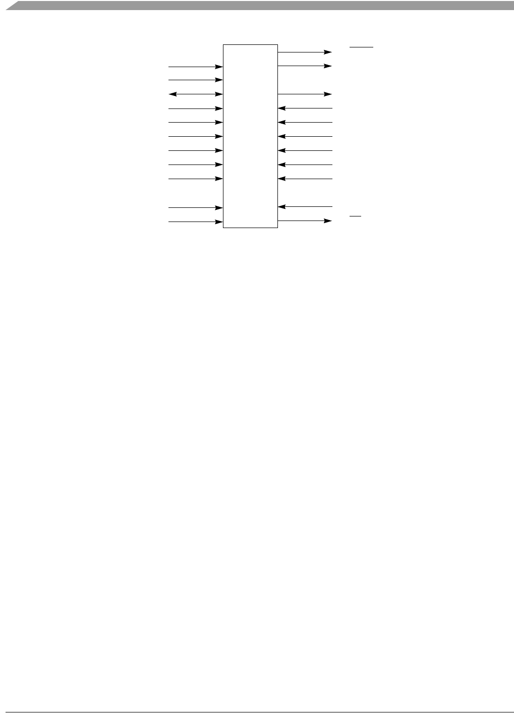
MCF548x Reference Manual, Rev. 3
8-64 Freescale Semiconductor
Figure 8-51. Recommended BDM Connector
1
3
5
7
9
11
13
15
17
19
21
23
25
2
4
6
8
10
12
14
16
18
20
22
24
26
Developer reserved 1
GND
GND
RESET
VDD_IO 2
GND
PSTDDATA6
PSTDDATA4
PSTDDATA2
PSTDDATA0
Freescale reserved
GND
VDD_CPU
BKPT
DSCLK
Developer reserved1
DSI
DSO
PSTDDATA7
PSTDDATA5
PSTDDATA3
PSTDDATA1
GND
Freescale reserved
PSTCLK
TA
1 Pins reserved for BDM developer use.
2 Supplied by target.

MCF548x Reference Manual, Rev. 3
Freescale Semiconductor i
Part II
System Integration Unit
Part II describes the system integration unit, which provides overall control of the bus and serves as the
interface between the ColdFire core processor complex and internal peripheral devices. It includes a
general description of the SIU and individual chapters that describe components of the SIU, such as the
interrupt controller, general purpose timers, slice timers, and GPIOs.
Contents
Part II contains the following chapters:
•Chapter 9, “System Integration Unit (SIU),” describes the SIU programming model, bus
arbitration, and system-protection functions for the MCF548x.
•Chapter 10, “Internal Clocks and Bus Architecture,” describes the clocking and internal buses of
the MCF548x and discusses the main functional blocks controlling the XL bus and the XL bus
arbiter
•Chapter 11, “General Purpose Timers (GPT),” describes the functionality of the four general
purpose timers, GPT0–GPT3.
•Chapter 12, “Slice Timers (SLT),” describes the two slice timers, shorter term periodic interrupts,
used in the MCF548x.
•Chapter 13, “Interrupt Controller,” describes operation of the interrupt controller portion of the
SIU. It includes descriptions of the registers in the interrupt controller memory map and the
interrupt priority scheme.
•Chapter 14, “Edge Port Module (EPORT),” describes EPORT module functionality.
•Chapter 15, “GPIO,” describes the operation and programming model of the parallel port pin
assignment, direction-control, and data registers.

MCF548x Reference Manual, Rev. 3
ii Freescale Semiconductor

MCF548x Reference Manual, Rev. 3
Freescale Semiconductor 9-1
Chapter 9
System Integration Unit (SIU)
9.1 Introduction
The system integration unit (SIU) of the MCF548x family integrates several timer functions required by
most embedded systems. The SIU contains the following components:
• Slice timers
• Watchdog timer
• General purpose timers
• General purpose I/O ports
• Interrupt controller
Two internal 32-bit slice timers are provided to create short cycle periodic interrupts, typically utilized for
RTOS scheduling and alarm functionality. A watchdog timer is included that will reset the processor if not
regularly serviced, catching software hang-ups. Up to four 32-bit general purpose timers are included,
which are capable of input capture, output compare, and PWM functionality. Most peripheral I/O pins on
the MCF548x family are muxed with GPIO, adding flexibility and usability to pins on the chip.
The programmable interrupt controller multiplexes the external interrupts, general purpose timers, slice
timers, and peripheral sources to the CF4e core. Refer to Chapter 13, “Interrupt Controller,” for
information about the MCF548x interrupt controller.
The SIU timers are discussed in the following chapters:
• General purpose timers and watchdog timer (GPT0) are described in Chapter 11, “General Purpose
Timers (GPT).”
— The watchdog timer is further detailed in Section 10.3.2.3, “Watchdog Functions.”
• Slice timers are detailed in Chapter 12, “Slice Timers (SLT).”
• GPIO functionality is discussed in Chapter 15, “GPIO.”
9.2 Features
The system integration unit has the following features:
• Interrupt controller
• Two 32-bit slice timers for periodic alarm and interrupt generation
• Software watchdog timer with programmable secondary bus monitor
• Up to four 32-bit general-purpose timers with capture, compare, and PWM capability
• General-purpose I/O ports multiplexed with peripheral pins
• System protection and reset status and control
9.3 Memory Map/Register Definition
Table 9-1 shows the programming model for the SIU.

MCF548x Reference Manual, Rev. 3
9-2 Freescale Semiconductor
9.3.1 Module Base Address Register (MBAR)
The supervisor-level MBAR, Figure 9-1, specifies the base address and allowable access types for all
internal peripherals. It is written with a MOVEC instruction using the CPU address 0xC0F (refer to the
ColdFire Family Programmer’s Reference Manual). MBAR can be read or written through the debug
modules as a read/write register, as described in Chapter 8, “Debug Support.” Only the debug module can
read MBAR.
The MBAR is initialized to 0x8000_0000 at reset; however, it can be relocated to a new base address. To
access internal peripherals, write MBAR with the appropriate base address (BA) after system reset.
All internal peripheral registers occupy a single relocatable memory block along 256-KByte boundaries.
MBAR[BA] is compared to the upper 14 bits of the full 32-bit internal address to determine if an internal
peripheral is being accessed. Any accesses in this range, whether to a valid peripheral address or not, will
be made internally rather than using the external bus.
NOTE
The MBAR region must be mapped to non-cacheable space.
Table 9-1. SIU Register Map
Address
(MBAR +) Name Byte0 Byte1 Byte2 Byte3 Access
CPU+0xC0F Module Base Address Register MBAR R/W
0x04 SDRAM Drive Strength Register1
1The SDRAM Drive Strength and Chip Select Configuration registers are discussed in Chapter 18, “SDRAM Controller
(SDRAMC).” They are shown in this memory map for reference purposes.
SDRAMDS1R/W
0x08–0x0C Reserved
0x10 System Breakpoint Control Regis-
ter
SBCR R/W
0x1–0x1C Reserved
0x20 SDRAM Chip Select 0
Configuration Register1CS0CFG01R/W
0x24 SDRAM Chip Select 1
Configuration Register1CS1CFG11R/W
0x28 SDRAM Chip Select 2
Configuration Register1CS2CFG21R/W
0x2C SDRAM Chip Select 3
Configuration Register1CS3CFG31R/W
0x30–0x34 RESERVED
0x38 Sequential Access Control Register SECSACR R/W
0x3C–0x40 RESERVED
0x44 Reset Status Register RSR R/W
0x48–0x4C RESERVED
0x50 JTAG Device Identification Number JTAGID R

Memory Map/Register Definition
MCF548x Reference Manual, Rev. 3
Freescale Semiconductor 9-3
9.3.1.1 System Breakpoint Control Register (SBCR)
The System Breakpoint Control Register allows for discrete control over functionality of the BKPT signal.
The assertion of the BKPT signal can be programmed to halt the core, DMA, and DSPI or any
combination. In addition, a halt condition in the DMA can be programmed to halt the CPU, or a halt in the
CPU can halt the DMA.
31 30 29 28 27 26 25 24 23 22 21 20 19 18 17 16
RBA 00
W
Reset1000000000000000
1514131211109876543210
R0000000000000000
W
Reset0000000000000000
Reg
Addr
CPU + 0xC0F
Figure 9-1. Module Base Address Register (MBAR)
31 30 29 28 27 26 25 24 23 22 21 20 19 18 17 16
RPIN2
CPU
PIN2
DMA
CPU2
DMA
DMA2
CPU
PIN2
DSPI
00000000000
W
Reset1100000000000000
1514131211109876543210
R0000000000000000
W
Reset0000000000000000
Reg
Addr
MBAR + 0x0010
Figure 9-2. System Breakpoint Control Register (SBCR)
Table 9-2. SBCR Field Descriptions
Bit Name Description
31 PIN2CPU Pin control of the ColdFire V4e breakpoint. This bit controls whether the BKPT pin can halt the
ColdFire V4e.
0 The assertion of BKPT will not halt the ColdFire V4e core.
1 The assertion of BKPT will halt the ColdFire V4e core.
30 PIN2DMA Pin control of the multichannel DMA breakpoint. This bit controls whether the BKPT pin can halt
the DMA.
0 The assertion of BKPT will not halt the DMA.
1 The assertion of BKPT will halt the DMA.

MCF548x Reference Manual, Rev. 3
9-4 Freescale Semiconductor
9.3.1.2 SEC Sequential Access Control Register (SECSACR)
This register is used to control bus accesses to the SEC module. If a sequential accesses to the SEC are
enabled, then data will be buffered to create a single 64-bit access to the SEC instead of splitting up the
transfer into two longwords. This can help to improve overall SEC performance.
29 CPU2DMA ColdFire V4e control of the multichannel DMA breakpoint. This bit controls whether a ColdFire
V4e halt condition causes the assertion of the DMA breakpoint.
0 A ColdFire V4e halt condition will not halt the DMA.
1 A ColdFire V4e halt condition will halt the DMA.
28 DMA2CPU DMA control of the ColdFire V4e breakpoint. This bit controls whether a DMA halt condition
causes the assertion of the ColdFire V4e breakpoint.
0 A DMA halt condition will not halt the ColdFire V4e.
1 A DMA halt condition will halt the ColdFire V4e.
27 PIN2DSPI Pin control of the DSPI breakpoint. This bit controls whether the BKPT pin can halt the DSPI.
0 The assertion of BKPT will not halt the DSPI.
1 The assertion of BKPT will halt the DSPI.
26-0 — Reserved, should be cleared.
31 30 29 28 27 26 25 24 23 22 21 20 19 18 17 16
R000000000000000 0
W
Reset000000000000000 0
151413121110987654321 0
R000000000000000SEQEN
W
Reset000000000000000 0
Reg
Addr
MBAR + 0x38
Figure 9-3. SEC Sequential Access Control Register (SECSACR)
Table 9-3. SECSACR Field Descriptions
Bits Name Description
31–1 — Reserved
0 SEQEN SEC Sequential access enable.
0 SEC Sequential Access is disabled.
1 SEC Sequential Access is enabled.
Note: Setting this bit is recommended when the SEC is in use.
Table 9-2. SBCR Field Descriptions (Continued)
Bit Name Description

Memory Map/Register Definition
MCF548x Reference Manual, Rev. 3
Freescale Semiconductor 9-5
9.3.1.3 Reset Status Register (RSR)
RSR allows the software, particularly the reset exception service routine, to know what type of reset has
been asserted. When a reset signal is asserted, the associated status bit is set, and it maintains its value until
the software explicitly clears the bit.
9.3.1.4 JTAG Device Identification Number (JTAGID)
31 30 29 28 27 26 25 24 23 22 21 20 19 18 17 16
R0000000000000000
W
Reset0000000000000000
1514131211109876543210
R000000000000RST
JTG
0RST
WD
RST
W
Reset0000000000000001
Reg
Addr
MBAR + 0x44
Figure 9-4. Reset Status Register (RSR)
Table 9-4. RSR Field Descriptions
Bits Name Description
31–4 — Reserved, should be cleared.
3 RSTJTG JTAG reset asserted. Cleared by writing 1 to this bit position or by external reset.
2 — Reserved, should be cleared.
1 RSTWD General purpose watchdog timer reset asserted. Cleared by writing 1 to this bit position or
by external reset.
0 RST External reset (PLL Lock qualification) asserted. Cleared by writing a 1 to this bit position.
31 30 29 28 27 26 25 24 23 22 21 20 19 18 17 16
RJTAGID
W
Reset See Table 9-5
1514131211109876543210
RJTAGID
W
Reset See Table 9-5
Reg
Addr
MBAR + 0x50
Figure 9-5. JTAG Device ID Register (JTAGID)

MCF548x Reference Manual, Rev. 3
9-6 Freescale Semiconductor
Table 9-5. JTAGID Field Descriptions
Bits Name Description
31–0 JTAGID The JTAG Identification Number Register is a read only register which contains the JTAG
ID number for the MCF548x. Its value is hard coded and cannot be modified.
Values for the MCF548x are the following:
MCF5485 0x0800c01d
MCF5484 0x0800d01d
MCF5483 0x0800e01d
MCF5482 0x0800f01d
MCF5481 0x0801001d
MCF5480 0x0801101d
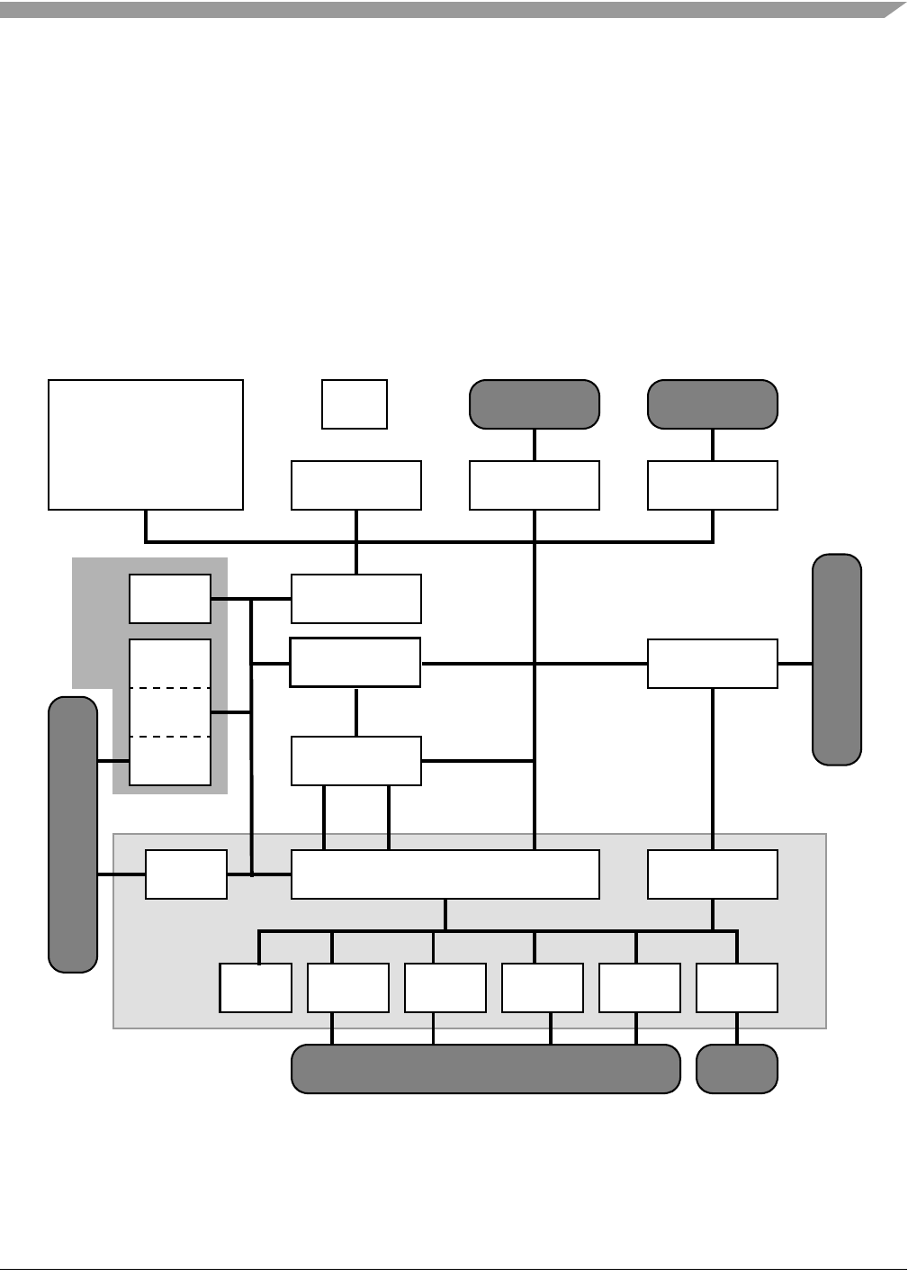
MCF548x Reference Manual, Rev. 3
Freescale Semiconductor 10-1
Chapter 10
Internal Clocks and Bus Architecture
10.1 Introduction
This chapter describes the clocking and internal buses of the MCF548x and discusses the main functional
blocks controlling the XL bus and the XL bus arbiter.
10.1.1 Block Diagram
Figure 10-1 shows a top-level block diagram of the MCF548x products.
*Available in MCF5485, MCF5484, MCF5483, and MCF5482 devices.
**Available in MCF5485, MCF5484, MCF5481, and MCF5480 devices.
***Available in MCF5485, MCF5483, and MCF5481 devices.
Figure 10-1. MCF548x Internal Bus Architecture
PLL DDR SDRAM
Memory
Controller
PCI I/O Interface and Ports
CommBus
USB 2.0
PHY*
Perpheral Communications I/O Interface & Ports
FEC1**PSC x 4I2CFEC0 USB 2.0
DEVICE*
Interface
FlexBus
Controller
FlexBus
Interface
PCI Interface
& FIFOs
Master/Slave
Interface
ColdFire V4e Core
FPU, MMU
EMAC
32K D-cache
32K I-cache
FlexCAN
x 2
Slave
Bus
DSPI
Perpheral I/O Interface & Ports
Communications
I/O Subsystem
Interrupt
Controller
XL Bus
Arbiter
System
Integration Unit
DMA
Read
DMA
Write
Multichannel DMA
Master Bus Interface and FIFOs
Slice
Timers x 2
GP
Timers x 4
Watchdog
Timer
PCI 2.2
Controller
Cryptography
32K System
SRAM
Crypto
R/W
XL Bus
Read/Write
XL Bus
Accelerator***
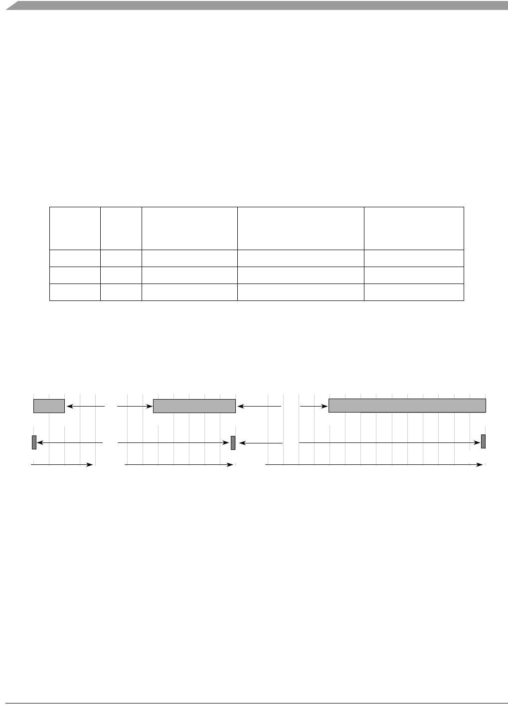
MCF548x Reference Manual, Rev. 3
10-2 Freescale Semiconductor
10.1.2 Clocking Overview
The MCF548x requires a clock generated externally to be input to the CLKIN signal. The MCF548x uses
this clock as the reference clock for the internal PLL. The internal PLL then generates the clocks needed
by the CPU core and integrated peripherals.
The external PCI and FlexBus signals are always clocked at the same frequency as the CLKIN signal. A
programmable clock multiplier (determined by the AD[12:8] signals at reset) is used to determine the XL
bus frequency. All integrated peripherals and the 32KB system SRAM are clocked at the same frequency
as the XLB. The ColdFire V4e core complex (core, MMU, FPU, SRAMs, etc.) is always clocked at twice
the XLB frequency.
Table 10-1 shows the supported PLL encodings and the corresponding clock frequency ranges.
Figure 10-2 correlates CLKIN, internal bus, and core clock frequencies for the 1x–4x multipliers.
Figure 10-2. CLKIN, Internal Bus, and Core Clock Ratios
10.1.3 Internal Bus Overview
There are three main internal buses in the MCF548x—the extended local bus (XL bus), the internal
peripheral bus (slave bus), and the communication subsystem bus (CommBus). See Figure 10-1.
• XL bus — Interface between the ColdFire core, memory controller, communication subsystem,
FlexBus controller, and PCI controller.
• Internal peripheral bus (slave bus) — The control/data interface from the core to the
communication subsystem or peripheral programming registers and FIFOs. The base address of
this memory-mapped bus will be stored in the internal peripheral bus base address register
(MBAR).
Table 10-1. MCF548x Divide Ratio Encodings
AD[12:8]1
1All other values of AD[12:8] are reserved.
Clock
Ratio
CLKIN–PCI and
FlexBus Frequency
Range (MHz)
Internal XLB, SDRAM bus,
and PSTCLK Frequency
Range (MHz)
Core Frequency
Range (MHz)
00011 1:2 41.6–50.0 83.33–100 166.66–200
00101 1:2 25.0–41.5 50.0–83.02
2Note that DDR memories typically have a minimum speed of 83 MHz. Some vendors specifiy down to
75 MHz. Check with the memory component specifications to verify.
100.0–166.66
01111 1:4 25.0 100 200
25 40 50 60 70 70 80 90 100 110 120 130 140 150 160 170 180 190 20060
25.0 50.0 100.0
CLKIN (MHz) Core Clock (MHz)
Core Clock
CLKIN
200.0
40 50 60 70 80 90 10030
50.0 100.0
Internal Clock
Internal Clock (MHz)
2x
2x
25.0 200.0
2x
4x
100.0

Introduction
MCF548x Reference Manual, Rev. 3
Freescale Semiconductor 10-3
• CommBus — The data transfer interface between the multichannel DMA and each peripheral
function.
10.1.4 XL Bus Features
Features of the XL bus and its integration modules include the following:
• 32-bit physical address
• 64-bit data bus width
• Split-transaction bus; address and data tenures occur independently.
• One-level address pipeline; supports up to two complete address tenures before the first data tenure
completes.
• Strict, in-order, address and data tenures are enforced.
• Address and data bus “parking” may be used to remove arbitration phase from the address and data
tenures—most recent master, programmed master, or no parking methods supported.
• Access can occur in single (1-8 bytes) beat, or four-beat (32 bytes) burst transfers.
• Eight-level arbitration priority that is hardware selectable for each master with a least recently used
(LRU) protocol for masters of equal priority. Priority may change dynamically based on specific
system requirements.
• Fully static, multiplexed bus architecture.
10.1.5 Internal Bus Transaction Summaries
The XL bus can be mastered by the ColdFire core, multichannel DMA controller, and the PCI controller
(external PCI master). Any of these masters can access all resources available to the XL bus.
Bus masters can access any on-chip or off-chip resources via the XL bus. The sequence is as follows:
• Bus masters gains mastership of the XL bus from the XL bus arbiter.
• The bus master’s address is asserted during the address tenure. XL bus slave devices (SDRAM,
PCI, etc.) decode the address. If the address falls within a slave’s space, it returns an address
acknowledge.
• The bus master initiates the data tenure and transfers the data to the appropriate slave device.
10.1.6 XL Bus Interface Operations
This section describes how the XLB interface operates.
10.1.6.1 Basic Transfer Protocol
An XLB interface memory transaction is illustrated in Figure 10-3. It shows that the transaction consists
of distinct address and data tenures, each having three phases: arbitration, transfer, and termination. The
separation of these operations allows address pipelines and split transactions to be implemented.
Split-bus transaction capability allows one master to have mastership of the address bus, while another
master has mastership of the data bus. Pipelines allows the address tenure of a bus transaction to begin
before the data tenure of the previous transaction finishes.
The data transfer phase can either be one beat or four, depending on whether or not the transaction is a
burst.

MCF548x Reference Manual, Rev. 3
10-4 Freescale Semiconductor
Figure 10-3. Address and Data Tenures
The following outlines the basic functions of each of the phases:
• Address tenure:
— Arbitration: During arbitration, address bus arbitration signals are used to gain mastership of
the address bus.
— Transfer: After mastership is obtained, the address bus master transfers the address and transfer
attributes on the address bus. Address signals and transfer attribute signals control the address
transfer.
— Termination: After the address transfer, the system signals that the address tenure is complete
or that it must be repeated.
• Data tenure:
— Arbitration: To begin a data tenure, the master arbitrates for data bus mastership.
— Transfer: After mastership is obtained, the data bus master samples the data bus for read
operations or drives the data bus for write operations.
— Termination: Data termination signals are required after each data beat in a data transfer. In a
single-beat transaction, data termination signals also indicate the end of the tenure; in burst
accesses, data termination signals apply to individual beats and indicate the end of the tenure
only after the final data beat.
10.1.6.2 Address Pipelines
The XLB protocol provides independent address and data bus capability to support pipeline and split-bus
transaction system organizations.
The XLB arbiter allows for one level of pipeline. This feature can be enabled and disabled in the Arbiter
Configuration Register (XARB_CFG). While this feature does not improve latency, it can significantly
improve bus/memory throughput, so it should be considered for systems that expect to stress bus
throughput capacity.
The XLB arbiter effects pipelines by regulating address bus grant, data bus grants, and address
acknowledge signals. For example, a one-level pipeline is enabled by asserting the address acknowledge
signal to the current address bus master, as well as granting the address bus to the next requesting master
before the current data bus tenure completes.
Arbitration Transfer Termination
Address Tenure
Arbitration Transfer Termination
Data Tenure

PLL
MCF548x Reference Manual, Rev. 3
Freescale Semiconductor 10-5
10.2 PLL
10.2.1 PLL Memory Map/Register Descriptions
10.2.2 System PLL Control Register (SPCR)
The system PLL control register (SPCR) defines the clock enables used to control clocks to a set of
peripherals. Unused peripherals can have their clock stopped, reducing power consumption. In addition,
the SPCR contains a read-only bit for the system PLL lock status. At reset, the clock enables are set,
enabling all system PLL gated output clocks.
Table 10-2. System PLL Memory Map
MBAR
Offset Name Byte0 Byte1 Byte2 Byte3 Access
0x300 System PLL Control Register SPCR R/W
31 30 29 28 27 26 25 24 23 22 21 20 19 18 17 16
RPLLK000000000000000
W
Reset1000000000000000
1514131211109876543210
R0
COR
EN
CRY
ENB
CRY
ENA
CAN1
EN
0PSC
EN
0USB
EN
FEC1
EN
FEC0
EN
DMA
EN
CAN0
EN
FB
EN
PCI
EN
MEM
EN
W
Reset 0111111111111111
Reg
Addr MBAR + 0x300
Figure 10-4. System PLL Control Register (SPCR)
Table 10-3. SPCR Field Descriptions
Bits Name Description
31 PLLK System PLL Lock Status - Read-only lock status of the system PLL.
1 PLL has obtained frequency lock
0 PLL has not locked
30-15 — Reserved, should be cleared.
14 COREN Core & Communications Sub-System Clock Enable - Controls clocks for the CF4 Core, System
SRAM, CommBus Arbiter, I2C, Comm Timers, and External DMA modules
13 CRYENB Crypto Clock Enable B - Controls the fast clock to the SEC
12 CRYENA Crypto Clock Enable A - Controls the slow clock to the SEC
11 CAN1EN CAN1 Clock Enable
10 — Reserved, should be cleared.

MCF548x Reference Manual, Rev. 3
10-6 Freescale Semiconductor
10.3 XL Bus Arbiter
The XL bus arbiter handles bus arbitration between XL bus masters.
10.3.1 Features
The arbiter features are as follows:
• Eight priority levels
• Priority levels may be changed dynamically by XL bus masters
• XL bus arbitration support for eight masters
• Least recently used (LRU) priority scheme for masters of equal priority
• Multiple masters at each priority level supported
• One level of address pipelines is enforced by the arbiter
• Bus grant parking modes:
— No parking
— Park on last master
— Park on programmed master
• Watchdog timers for various XL bus time-out conditions
10.3.2 Arbiter Functional Description
10.3.2.1 Prioritization
The prioritization function will indicate that a master is requesting the bus and indicate which master has
priority.
Priority is determined first by using the hardcoded master priority or the master n priority bits in the arbiter
master priority register (XARB_PRIEN), depending on the arbiter master priority enable bit for each
master. Secondly, masters at the same level of priority will be further sorted by a least recently used
9 PSCEN PSC Clock Enable - Controls clock for all PSC modules.
8 — Reserved, should be cleared.
7 USBEN USB Clock Enable
6 FEC1EN FEC1 Clock Enable
5 FEC0EN FEC0 Clock Enable
4 DMAEN Multi-channel DMA Clock Enable
3 CAN0EN CAN0 Clock Enable
2 FBEN FlexBus Clock Enable
1 PCIEN PCI Bus Clock Enable
0 MEMEN Memory Clock Enable - Controls clocks of the SDRAM controller module
Table 10-3. SPCR Field Descriptions (Continued)
Bits Name Description

XL Bus Arbiter
MCF548x Reference Manual, Rev. 3
Freescale Semiconductor 10-7
algorithm (LRU). Once a requesting master is identified as having priority and is granted the bus, that
master will be continue to be granted the bus if:
1. It is requesting the bus. The request must occur immediately after the required 1 clock de-assertion
after a qualified bus grant.
and
2. It is the highest priority device.
and
3. There is no address retry.
Multiple masters at level 0 will only be able to perform one tenure before the bus is passed to the next
master at level 0 using the LRU algorithm.
The priority level of each master may be changed while the arbiter is running. This allows dynamic
changes in priority such as an aging scheme. The arbiter recognizes changes after one clock.
It is possible to control priority by enabling the master priority enable bits for a master (XARB_PRIEN).
This causes the priority to be determined from the master n priority bits in the arbiter master priority
register (XARB_PRI). Once again a system dependent dynamic scheme may be employed.
10.3.2.2 Bus Grant Mechanism
10.3.2.2.1 Bus Grant
The bus grant mechanism generates the address bus grant signals to the masters using the signals from the
prioritization function. It will also generate required indicators of state to the prioritization and watchdog
functions.
The bus grant mechanism will enforce the one level address pipeline. The critical condition is that before
a third address tenure is granted, the first tenure (address and, if needed, data) must be completed. The
arbiter will assert a bus grant to a master when there are masters requesting, or if parking is enabled and
the one level pipeline condition is met.
10.3.2.2.2 Parking Modes
The bus grant mechanism will support the no parking, park on programmed master, and park on last master
bus parking modes.
• When in no parking mode, the arbiter will not assert a bus grant when there are no masters asserting
a bus request.
• In park on programmed master mode, the arbiter will assert a bus grant to the master indicated in
the select parked master field (ACFG[SP]) when no masters are asserting a bus request and the one
level pipeline will not be violated.
• In park on last master mode, the arbiter will assert a bus grant to the last master granted the bus
when no masters are asserting a bus request and the one level pipeline will not be violated.

MCF548x Reference Manual, Rev. 3
10-8 Freescale Semiconductor
10.3.2.3 Watchdog Functions
10.3.2.3.1 Timer Functions
There are three watchdog timers: address tenure time out, data tenure time out, and bus activity time out.
Each has a programmable timer count and can be disabled. A timer time-out will set a status bit and trigger
an interrupt if that interrupt is enabled.
• The address tenure watchdog is a 32-bit timer. If an acknowledge is not detected by the
programmed number of clocks after bus grant is accepted, the address watchdog timer will expire
and the arbiter will issue an acknowledge. The related data tenure will be terminated with a transfer
error acknowledge. The arbiter will set the Address Tenure Time-out Status bit in the arbiter status
register and issue an interrupt if that interrupt is enabled.
The upper 28 bits of address tenure time-out are programmed via the address tenure time-out
register. The lower 4 bits are always 0xF.
• The data tenure watchdog is a 32-bit timer. If a data tenure is not terminated, the data watchdog
timer will expire and the arbiter will issue a transfer error acknowledge. The arbiter will set the
Data Tenure Time-out Status bit in the arbiter status register and issue an interrupt if that interrupt
is enabled.
Address Time-out (32 bits) = {address tenure time-out register (28bits), 0xF}
Data Time-out (32 bits) = {data tenure time-out register (28 bits), 0xF}
• The bus activity watchdog is a 32-bit timer. If no bus activity is detected by the programmed
number of clocks, the bus activity watchdog timer will expire and the arbiter will set the Bus
Activity Time-out Status bit in the arbiter status register and issue an interrupt if that interrupt is
enabled.
NOTE
Enabling the data time-out will also enable the address time-out. It is
recommended that the data watchdog timer should always be programmed
to a value that is larger than the address watchdog timer. This prevents the
XL bus arbiter from generating a transfer error acknowledge due to
expiration of the data watchdog timer while the address tenure has not
completed.
10.3.3 XLB Arbiter Register Descriptions
The XLB Arbiter registers and their locations are defined in Table 10-4.
Table 10-4. XL Bus Arbiter Memory Map
MBAR
Offset Name Byte0 Byte1 Byte2 Byte3 Access
0x240 Arbiter Configuration Register XARB_CFG R/W
0x244 Arbiter Version Register XARB_VER R
0x248 Arbiter Status Register XARB_SR R/W
0x24C Arbiter Interrupt Mask Register XARB_IMR R/W
0x250 Arbiter Address Capture XARB_ADRCAP R/W
0x254 Arbiter Signal Capture XARB_SIGCAP R/W

XL Bus Arbiter
MCF548x Reference Manual, Rev. 3
Freescale Semiconductor 10-9
10.3.3.1 Arbiter Configuration Register (XARB_CFG)
The arbiter configuration register is used to enable watchdog functions and arbiter protocol functions.
0x258 Arbiter Address Timeout XARB_ADRTO R/W
0x25C Arbiter Data Timeout XARB_DATTO R/W
0x260 Arbiter Bus Timeout XARB_BUSTO R/W
0x264 Arbiter Master Priority Enable XARB_PRIEN R/W
0x268 Arbiter Master Priority XARB_PRI R/W
31 30 29 28 27 26 25 24 23 22 21 20 19 18 17 16
RPLDIS000000000000000
W
Reset1 000000000000000
1514131211109876543210
R0 0 000SP 0 PM 0 BA DT AT 0
W
Reset0 000000000000110
Reg
Addr
MBAR + 0x0240
Figure 10-5. Arbiter Configuration Register (XARB_CFG)
Table 10-5. XARB_CFG Bit Descriptions
Bit Name Description
31 PLDIS Pipeline Disable. This bit is used to control the pipeline functionality
0 Enable pipeline
1 Disable pipeline
30–11 — Reserved, should be cleared.
10–8 SP Select Parked Master. These bits set the master that is used in Park on Programmed Master mode.
000 Master 0
001 Master 1
...
111 Master 7).
7 — Reserved, should be cleared.
6–5 PM[1:0] Parking Mode. Parking modes are detailed in Section 10.3.2.2.2, “Parking Modes.”
00 No parking (default)
01 Reserved
10 Park on most recently used master
11 Park on programmed master as specified by the Select Parked Master bits 21:23 above.
Table 10-4. XL Bus Arbiter Memory Map (Continued)
MBAR
Offset Name Byte0 Byte1 Byte2 Byte3 Access

MCF548x Reference Manual, Rev. 3
10-10 Freescale Semiconductor
10.3.3.2 Arbiter Version Register (XARB_VER)
4 — Reserved, should be cleared.
3 BA Bus Activity Time-out Enable. If enabled, the arbiter will set the Bus Activity Time-out Status bit
(XARB_SR[BA]) when the Bus Activity Time-out is reached. Bus Activity Time-out is derived from
the arbiter bus activity time out count register.
0 Disable bus activity time-out
1 Enable bus activity time-out
2 DT Data Tenure Time-out Enable. If enabled, the arbiter will transfer error acknowledge when the Data
Tenure Time-out is reached. Data Tenure Time-out is derived from the arbiter data tenure time out
count register. Also, the arbiter will set the Data Tenure Time-out Status bit (Arbiter Status Register
Bit 30). Setting this bit will also enable the Address Tenure Time-out. This is required to ensure that
a data time-out will not occur before an address acknowledge.
0 Disable data tenure time-out
1 Enable data tenure time-out
1 AT Address Tenure Time-out Enable. If enabled, the arbiter will AACK and TEA (if required) when the
Address Tenure Time-out is reached. Address Tenure Time-out is derived from the Arbiter Address
Tenure Time Out Count register. Also, the arbiter will set the Address Tenure Time-out Status bit
(Arbiter Status Register Bit 31). Address Tenure Time-out is also enabled by the DT bit above.
0 Disable address tenure time-out
1 Enable address tenure time-out
0 — Reserved, should be cleared.
31 30 29 28 27 26 25 24 23 22 21 20 19 18 17 16
R VER
W
Reset0000000000000000
1514131211109876543210
R VER
W
Reset0000000000000001
Reg
Addr
MBAR + 0x0244
Figure 10-6. Arbiter Version Register (XARB_VER)
Table 10-6. VER Field Descriptions
Bit Name Description
31–0 VER Hardware Version ID. The current version number is 0x0001.
Table 10-5. XARB_CFG Bit Descriptions (Continued)
Bit Name Description

XL Bus Arbiter
MCF548x Reference Manual, Rev. 3
Freescale Semiconductor 10-11
10.3.3.3 Arbiter Status Register (XARB_SR)
The arbiter status register indicates the state of watchdog functions. When a monitored condition occurs,
the respective bit is set to 1. The bit will stay set until the bit is cleared by writing a 1 into that bit. Even if
the causal condition is removed, the bit will remain set until cleared.
10.3.3.4 Arbiter Interrupt Mask Register (XARB_IMR)
The arbiter interrupt mask register is used to enable a status bit to cause an interrupt. If the interrupt mask
and corresponding status bits are set in the arbiter status register and arbiter interrupt mask register, the
arbiter will assert the interrupt signal. Normally, an interrupt service routine would read the status register
31 30 29 28 27 26 25 24 23 22 21 20 19 18 17 16
R0000000000000000
W
Reset0000000000000000
1514131211109876543210
R0000000SEAMMTTATTRECWTTMBADTAT
W
Reset0000000000000000
Reg
Addr
MBAR + 0x0248
Figure 10-7. Arbiter Status Register (XARB_SR)
Table 10-7. XARB_SR Field Descriptions
Bits Name Description
31–9 — Reserved, should be cleared.
8 SEA Slave Error Acknowledge. This bit is set when an error is detected by any slave devices during the
transfer.
7 MM Multiple Masters at priority 0. If more than 1 master is recognized at priority 0, this bit is set. Once this
occurs this bit will remain set until cleared. This bit is intended to help in tuning dynamic priority
algorithm development.
6 TTA TT Address Only. The arbiter automatically AACKs for address only TT codes. This bit is set when this
occurs.
5 TTR TT Reserved. The arbiter automatically AACKs for reserved TT codes. This bit is set when this occurs.
4 ECW External Control Word Read/Write. External Control Word Read/Write operations are not supported
on the XL bus. If either occur, the arbiter AACKs and TEAs and sets this bit.
3 TTM TBST/TSIZ mismatch. Set when an illegal/reserved TBST and TSIZ[0:2] combination occurs. These
combinations are TBST asserted and TSIZ[0:2] = 000, 001, 011, or 1xx (x is 0 or 1).
2 BA Bus Activity Tenure Time-out. Set when the bus activity time-out counter expires.
1 DT Data Tenure Time-out. Set when the data tenure time-out counter expires.
0 AT Address Tenure Time-out. Set when the address tenure time-out counter expires.

MCF548x Reference Manual, Rev. 3
10-12 Freescale Semiconductor
to determine the state of the arbiter. It is possible that multiple conditions exist that would cause an
interrupt. Disabling an interrupt by writing a 0 to a bit in this register will not clear the status bit in the
arbiter status register.
31 30 29 28 27 26 25 24 23 22 21 20 19 18 17 16
R00000000000 0 0000
W
Reset00000000000 0 0000
15 14 13 12 11 10 9 8 7 6 5 4 3 2 1 0
R0000000SEAE MME TTAE TTRE ECWE TTME BAE DTE ATE
W
Reset00000000000 0 0000
Reg
Addr
MBAR + 0x024C
Figure 10-8. Arbiter Interrupt Mask Register (XARB_IMR)
Table 10-8. XARB_IMR Field Descriptions
Bits Name Description
31–9 — Reserved, should be cleared.
8 SEAE Slave Error Acknowledge interrupt enable.
0 The corresponding interrupt source is masked.
1 The corresponding interrupt source is enabled.
7 MME Multiple Masters at priority 0 interrupt enable.
0 The corresponding interrupt source is masked.
1 The corresponding interrupt source is enabled.
6 TTAE TT Address Only interrupt enable.
0 The corresponding interrupt source is masked.
1 The corresponding interrupt source is enabled.
5 TTRE TT Reserved interrupt enable.
0 The corresponding interrupt source is masked.
1 The corresponding interrupt source is enabled.
4 ECWE External Control Word Read/Write interrupt enable.
0 The corresponding interrupt source is masked.
1 The corresponding interrupt source is enabled.
3 TTME TBST/TSIZ mismatch interrupt enable.
0 The corresponding interrupt source is masked.
1 The corresponding interrupt source is enabled.
2 BAE Bus Activity Tenure Time-out interrupt enable.
0 The corresponding interrupt source is masked.
1 The corresponding interrupt source is enabled.

XL Bus Arbiter
MCF548x Reference Manual, Rev. 3
Freescale Semiconductor 10-13
10.3.3.5 Arbiter Address Capture Register (XARB_ADRCAP)
The arbiter address capture register will capture the address for a tenure that has an address time-out, data
time-out, or there is a transfer error acknowledge from another source. This value is held until unlocked
by writing any value to the arbiter address capture register or arbiter bus signal capture register. This value
is also unlocked by writing a 1 to either XARB_SR[DT] or XARB_SR[AT]. Unlocking the register does
not clear its contents.
10.3.3.6 Arbiter Bus Signal Capture Register (XARB_SIGCAP)
Important bus signals are captured when a bus error occurs. This happens on an address time-out, data
time-out, or any transfer error acknowledge.
The arbiter bus signal capture register will capture TT, TBST, and TSIZ for a tenure that has an address
time-out or data time-out, or there is a transfer error acknowledge from another source. These values are
held until unlocked by writing any value to the arbiter address capture register (XARB_ADRCAP) or
arbiter bus signal capture register (XARB_SIGCAP). These values are also unlocked by writing a 1 to
either XARB_SR[DT] or XARB_SR[AT]. Unlocking the register does not clear its contents.
1 DTE Data Tenure Time-out interrupt enable.
0 The corresponding interrupt source is masked.
1 The corresponding interrupt source is enabled.
0 ATE Address Tenure Time-out interrupt enable.
0 The corresponding interrupt source is masked.
1 The corresponding interrupt source is enabled.
31 30 29 28 27 26 25 24 23 22 21 20 19 18 17 16
RADRCAP
W
Reset0000000000000000
1514131211109876543210
RADRCAP
W
Reset0000000000000000
Reg
Addr
MBAR + 0x0250
Figure 10-9. Arbiter Address Capture Register (XARB_ADRCAP)
Table 10-9. XARB_ADRCAP Field Descriptions
Bits Name Description
31–0 ADRCAP Address that is captured when a bus error occurs. This happens on an address time-out,
data time-out, or any transfer error acknowledge.
Table 10-8. XARB_IMR Field Descriptions (Continued)
Bits Name Description

MCF548x Reference Manual, Rev. 3
10-14 Freescale Semiconductor
10.3.3.7 Arbiter Address Tenure Time Out Register (XARB_ADRTO)
31 30 29 28 27 26 25 24 23 22 21 20 19 18 17 16
R0000000000000000
W
Reset0000000000000000
1514131211109876543210
R000000 TSIZ[0:2] —TBST TT[0:4]
W
Reset0000000000000000
Reg
Addr
MBAR + 0x0254
Figure 10-10. Arbiter Bus Signal Capture Register (XARB_SIGCAP)
Table 10-10. XARB_SIGCAP Field Descriptions
Bits Name Description
31–10 — Reserved, should be cleared.
9–7 TSIZ[0:2] TSIZ[0:2]
6 — Reserved, should be cleared
5 TBST TBST
4–0 TT TT[0:4]
31 30 29 28 27 26 25 24 23 22 21 20 19 18 17 16
R0000 ADRTO
W
Reset0000111111111111
1514131211109876543210
RADRTO
W
Reset1111111111111111
Reg
Addr
MBAR + 0x0258
Figure 10-11. Arbiter Address Tenure Time Out Register (XARB_ADRTO)

XL Bus Arbiter
MCF548x Reference Manual, Rev. 3
Freescale Semiconductor 10-15
10.3.3.8 Arbiter Data Tenure Time Out Register (XARB_DATTO)
Table 10-11. XARB_ADRTO Field Descriptions
Bits Name Description
31–28 — Reserved, should be cleared.
27–0 ADRTO Upper 28-bits of the Address time-out counter value. This field is prepended to 0xF to
generate the full 32-bit time-out counter value.
31 30 29 28 27 26 25 24 23 22 21 20 19 18 17 16
R0000 DATTO
W
Reset0000111111111111
1514131211109876543210
RDATTO
W
Reset1111111111111111
Reg
Addr
MBAR + 0x025C
Figure 10-12. Arbiter Data Tenure Time Out Register (XARB_DATTO)
Table 10-12. XARB_DATTO Field Descriptions
Bits Name Description
31–28 — Reserved, should be cleared.
27–0 DATTO Upper 28-bits fo the Data time-out counter value. This field is prepended to 0xF to generate
the full 32-bit time-out counter value.

MCF548x Reference Manual, Rev. 3
10-16 Freescale Semiconductor
10.3.3.9 Arbiter Bus Activity Time Out Register (XARB_BUSTO)
10.3.3.10 Arbiter Master Priority Enable Register (XARB_PRIEN)
The arbiter master priority enable register determines whether the arbiter uses the hardwired or software
programmable priority for a master. The default is enabled for all masters. Both methods may be used at
the same time for different masters. This register may be written at any time. The change will become
effective 1 clock after the register is written.
31 30 29 28 27 26 25 24 23 22 21 20 19 18 17 16
RBUSTO
W
Reset 1 1 1 1 1 1 1 1 1 1 1 1 1 1 1 1
15 14 13 12 11 10 9 8 7 6 5 4 3 2 1 0
RBUSTO
W
Reset 1 1 1 1 1 1 1 1 1 1 1 1 1 1 1 1
Reg
Addr
MBAR + 0x0260
Figure 10-13. Arbiter Bus Activity Time Out Register (XARB_BUSTO)
Table 10-13. XARB_BUSTO Field Descriptions
Bits Name Description
31–0 BUSTO Bus activity time-out counter value in XLB clocks.
31 30 29 28 27 26 25 24 23 22 21 20 19 18 17 16
R0000000000000000
W
Reset0000000000000000
1514131211109876543210
R00000000————M3M2—M0
W
Reset0000000011111111
Reg
Addr
MBAR + 0x0264
Figure 10-14. Arbiter Master Priority Enable Register (XARB_PRIEN)

XL Bus Arbiter
MCF548x Reference Manual, Rev. 3
Freescale Semiconductor 10-17
When enabled, the software programmable value in the arbiter master priority register (XARB_PRI) is
used as the priority for the master. When disabled, the master’s priority is determined as follows:
10.3.3.11 Arbiter Master Priority Register (XARB_PRI)
The master n priority bits of the arbiter master priority register are used to set the priority of each master
if the corresponding arbiter master priority enable register bit is enabled. This XARB_PRI register, in
conjunction with the arbiter master priority enable (XARB_PRIEN) register, allows master priorities to be
set, ignoring the hardcoded priority. This register may be written at anytime. The change will become
effective 1 clock after the register is written. Valid values are from 0 to 7, with 0 being the highest priority.
Table 10-14. XARB_PRIEN Field Descriptions
Bits Name Description
31–4 — Reserved, should be cleared.
3 M3 Master 3 Priority Register Enable
2 M2 Master 2 Priority Register Enable
1 — Reserved, should be cleared.
0 M0 Master 0 Priority Register Enable
Table 10-15. Hardcoded Master Priority
Master Priority Description
M7–M4 — Unused
M3 7 PCI Target Interface
M2 7 Multichannel DMA
M1 — Unused
M0 7 ColdFire core
31 30 29 28 27 26 25 24 23 22 21 20 19 18 17 16
R0 Reserved 0 Reserved 0 Reserved 0 Reserved
W
Reset0111011101110111
1514131211109876543210
R0 M3 Priority 0 M2 Priority 0 Reserved 0 M0 Priority
W
Reset0111011101110111
Reg
Addr
MBAR + 0x0268
Figure 10-15. Arbiter Master Priority Register (XARB_PRI)

MCF548x Reference Manual, Rev. 3
10-18 Freescale Semiconductor
Table 10-16. XARB_PRI Field Descriptions
Bits Name Description
31–15 — Reserved, should be cleared.
14–12 M3P Master 3 Priority
11 — Reserved, should be cleared.
10–8 M2P Master 2 Priority
7–3 — Reserved, should be cleared.
2–0 M0P Master 0 Priority

MCF548x Reference Manual, Rev. 3
Freescale Semiconductor 11-1
Chapter 11
General Purpose Timers (GPT)
11.1 Introduction
This chapter describes the operation of the MCF548x general purpose timers.
11.1.1 Overview
The MCF548x has four general-purpose timers (GPT[0:3]) that are configurable for the following
functions:
• Input capture
• Output capture
• Pulse width modulation (PWM) output
•Simple GPIO
• Internal CPU timer
• Watchdog timer (on GPT0 only)
Timer modules run off the internal peripheral bus clock. Each timer is associated to a single I/O signal.
Each timer has a 16-bit prescaler and 16-bit counter, thus achieving a 32-bit range (but only 16-bit
resolution).
11.1.2 Modes of Operation
The following gives a brief description of the available GPT modes:
1. Input Capture—When enabled in this mode, the counters run until the specified capture event
occurs (rise, fall, or pulse) on TIN[3:0]. At the capture event, the counter value is latched in the
status register. When this occurs, a CPU interrupt is generated.
2. Output Capture—When enabled in this mode, the counters run until they reach the programmed
terminal count value. At this point, the specified output event is generated (toggle, pulse high, or
pulse low) on TOUT[3:0]. When this occurs, a CPU interrupt is generated.
3. PWM (pulse width modulation)—In this mode the user can program period and width values to
create an adjustable, repeating output waveform on TOUT[3:0]. A CPU interrupt can be
generated at the beginning of each PWM period, at which time a new width value can be loaded.
The new width value, which represents “ON time,” is automatically applied at the beginning of
the next period. This mode is suitable for PWM audio encoding.
4. Simple GPIO—In this mode TOUT[3:0] and TIN[3:0] operate as a GPIO. Either TOUT[3:0] or
TIN[3:0] are specified, according to the programmable GPIO field. GPIO mode is mutually
exclusive of modes 1 through 3 (listed above). In GPIO mode, modes 5 through 6 (listed below)
remain available.
5. CPU Timer—The I/O signal is not used in this mode. Once enabled, the counters run until they
reach a programmed terminal count. When this occurs, an interrupt can be generated to the CPU.
This timer mode can be used simultaneously with the simple GPIO mode.

MCF548x Reference Manual, Rev. 3
11-2 Freescale Semiconductor
6. Watchdog Timer—This is a special CPU timer mode, available only on GPT0. The user must
enable the watchdog timer mode, which is not active upon reset. The terminal count value is
programmable. If the counter is allowed to expire, a full reset occurs. To prevent the watchdog
timer from expiring, software must periodically write 0xA5 to the GMS0[OCPW] field. This
causes the counter to reset.
11.2 External Signals
The GPT signals are the following:
• TIN[3:0]—External timer input
• TOUT[3:0]—External timer output
11.3 Memory Map/Register Definition
Each GPT uses four 32-bit registers. These registers are located at MBAR + the GPT offset 0x800.
Table 11-1 summarizes the GPT control registers.
Table 11-1. General Purpose Timer Memory Map
Address
(MBAR +) Name Byte 0 Byte 1 Byte 2 Byte 3 Access
0x800 GPT Enable and Mode Select Register 0 GMS0 R/W
0x804 GPT Counter Input Register 0 GCIR0 R/W
0x808 GPT PWM Configuration Register 0 GPWM0 R/W
0x80C GPT Status Register 0 GSR0 R
0x810 GPT Enable and Mode Select Register 1 GMS1 R/W
0x814 GPT Counter Input Register 1 GCIR1 R/W
0x818 GPT PWM Configuration Register 1 GPWM1 R/W
0x81C GPT Status Register 1 GSR1 R
0x820 GPT Enable and Mode Select Register 2 GMS2 R/W
0x824 GPT Counter Input Register 2 GCIR2 R/W
0x828 GPT PWM Configuration Register 2 GPWM2 R/W
0x82C GPT Status Register 2 GSR2 R
0x830 GPT Enable and Mode Select Register 3 GMS3 R/W
0x834 GPT Counter Input Register 3 GCIR3 R/W
0x838 GPT PWM Configuration Register 3 GPWM3 R/W
0x83C GPT Status Register 3 GSR3 R

Memory Map/Register Definition
MCF548x Reference Manual, Rev. 3
Freescale Semiconductor 11-3
11.3.1 GPT Enable and Mode Select Register (GMSn)
31 30 29 28 27 26 25 24 23 22 21 20 19 18 17 16
R OCPW 0 0 OCT 0 0 ICT
W
Reset0000000000000000
1514131211109876543210
RWDE
N
00CE 0 SC OD IEN 0 0 GPIO 0 TMS
W
Reset0000000000000000
Reg
Addr
MBAR + 0x800 (GMS0), 0x810 (GMS1), 0x820 (GMS2), 0x830 (GSM3)
Figure 11-1. GPT Enable and Mode Select Register (GMSn)
Table 11-2. GMSn Field Descriptions
Bits Name Description
31–24 OCPW Output capture pulse width. Applies to OC pulse types only. This field specifies the number of clocks
(non-prescaled) to create a short output pulse at each output event. This pulse is generated at the
end of the output capture period and overlays the next OC period (rather than adding to the period).
This field is alternately used as the watchdog reset field if watchdog timer mode is enabled.
23–22 — Reserved, should be cleared.
21–20 OCT Output capture type. Describes action to occur at each output capture event, as follows:
00 Special case, output is immediately forced low without respect to each output capture event.
01 Output pulses highs, initial value is low (OCPW field applies).
10 Output pulses low, initial value is high (OCPW field applies).
11 Output toggles.
GPIO modalities can be used to achieve an initial output state prior to enabling OC mode. It is
important to move directly from GPIO output mode to OC mode and not to pass through the
TMS=000 state.
To prevent the internal timer mode from engaging during the GPIO state, CE bit should be cleared
during the configuration steps.
GPIO initialization is needed when presetting the I/O to 1 in conjunction with a simple toggle OCT
setting.
19–18 — Reserved, should be cleared.
17–16 ICT Input capture type. Describes the input transition type required to trigger an input capture event, as
follows:
00 Any input transition causes an IC event.
01 IC event occurs at input rising edge.
10 IC event occurs at input falling edge.
11 IC event occurs at any input pulse (i.e., at the second input edge).

MCF548x Reference Manual, Rev. 3
11-4 Freescale Semiconductor
15 WDEN Watchdog enable. Enables watchdog operation. A timer expiration causes an internal MCF548x
reset. Watchdog operation requires the TMS field be set for internal timer mode and the CE bit to be
set.
In this mode the OCPW byte field operates as a watchdog reset field. Writing A5 to the OCPW field
resets the watchdog timer, preventing it from expiring. As long as the timer is properly configured, the
watchdog operation continues.
This bit (and functionality) is implemented only for GPT0.
0 Watchdog not enabled
1 Watchdog enabled
14–13 — Reserved, should be cleared.
12 CE Counter enable. Enables or resets the internal counter during internal timer modes only. CE must be
set to enable these modes. If cleared, counter is held in reset.
0 Timer counter held in reset
1 Timer counter enabled
This bit is secondary to the timer mode select bits (TMS). If TMS is1XX, internal timer modes are
enabled. CE can then enable or reset the internal counter without changing the TMS field.
GPIO operation is also available in this mode.
11 — Reserved, should be cleared.
10 SC Stop/continuous mode.
0 Stops the operation
1 Continues the operation
The SC bit applies to multiple modes, as follows:
IC mode (input capture mode)
Stop operation—At each IC event, counter is reset.
Continuous operation—counter is not reset at each IC event.
Effect is to create status count values that are cumulative between capture events. If the special pulse
mode capture type is specified, the SC bit is not used, operation fixed as if it were stop.
OC mode (output capture mode)
Stop operation—Counter resets and stops at the first output capture event. Software needs to pass
through TMS=000 state to restart timer.
Continuous operation—counter resets and continues at each OC event. The effect to is create
back-to-back periodic OC events.
PWM mode (pulse width modulation mode)
The SC bit is not used; operation is always continuous.
CPU Timer mode
Stop operation—On counter expiration, timer waits until status bit is cleared by passing through
TMS=000 state before beginning a new cycle.
Continuous operation—On counter expiration, timer resets and immediately begin a new cycle. The
effect is to generate fixed periodic timeouts.
WatchDog Timer and GPIO modes
The SC bit is not used.
9 OD Open drain.
0Normal I/O
1 Open Drain emulation—affects all modes that drive the I/O pin (GPIO, OC, and PWM). Any output
“1” is converted to a tri-state at the I/O pin.
Table 11-2. GMSn Field Descriptions (Continued)
Bits Name Description

Memory Map/Register Definition
MCF548x Reference Manual, Rev. 3
Freescale Semiconductor 11-5
11.3.2 GPT Counter Input Register (GCIRn)
8 IEN Interrupt enable. Enables interrupt generation to the CPU for all modes (IC, OC, PWM, and Internal
Timer). IEN is not required for watchdog expiration to create a reset.
0 Interrupt disabled
1 Interrupt enabled
7–6 — Reserved, should be cleared.
5–4 GPIO GPIO mode type. Simple GPIO functionality that can be used simultaneously with the internal timer
mode. It is not compatible with IC, OC, or PWM modes, because these modes dictate the usage of
the I/O signals.
0X Timer enabled as simple GPIO input on TINn
10 Timer enabled as simple GPIO output, TOUTn=0
11 Timer enabled as simple GPIO output, TOUTn=1 (tri-state if OD=1)
While in GPIO modes, internal timer mode is also available. To prevent undesired timer expiration,
keep the CE bit cleared.
3 — Reserved, should be cleared.
2–0 TMS Timer mode select (and module enable).
000 Timer module not enabled. All timer operation is completely disabled. Control and status
registers are still accessible. This mode should be entered when the timer is to be re-configured,.
001 Timer enabled for input capture.
010 Timer enabled for output capture.
011 Timer enabled for PWM.
1XX Timer enabled for simple GPIO. Internal timer modes available. CE bit controls timer counter.
31 30 29 28 27 26 25 24 23 22 21 20 19 18 17 16
RPRE
W
Reset0000000000000000
1514131211109876543210
RCNT
W
Reset0000000000000000
Reg
Addr
MBAR + 0x804 (GCIR0), 0x814 (GCIR1), 0x824 (GCIR2), 0x834 (GCIR3)
Figure 11-2. GPT Counter Input Register (GCIRn)
Table 11-2. GMSn Field Descriptions (Continued)
Bits Name Description

MCF548x Reference Manual, Rev. 3
11-6 Freescale Semiconductor
11.3.3 GPT PWM Configuration Register (GPWMn)
Table 11-3. GCIRn Field Descriptions
Bits Name Description
31–16 PRE Prescaler. Prescale amount applied to internal counter (in clocks).
Note that in addition to other enable bits and field settings, the PRE field must be written as
non-zero to enable counter operation for all modes except the simple GPIO mode. A prescale of
0x0001 means one clock per count increment.
15–0 CNT Count value. Sets number of prescaled counts applied to reference events, as follows:
IC—Field has no effect, internal counter starts at 0.
OC—Number of prescaled counts counted before creating output event.
PWM—Number of prescaled counts defining the PWM output period.
Internal Timer—Number of prescaled counts counted before timer (or watchdog) expires.
Reading this register only returns the programmed value, intermediate values of the internal
counter are not available to software.
31 30 29 28 27 26 25 24 23 22 21 20 19 18 17 16
RWIDTH
W
Reset0000000000000000
1514131211109876543210
R0000000PWM
OP
0000000LOAD
W
Reset0000000000000000
Reg
Addr
MBAR + 0x808 (GPWM0), 0x818 (GPWM1), 0x828 (GPWM2), 0x838 (GPWM3)
Figure 11-3. GPT PWM Configuration Register (GPWMn)
Table 11-4. GPWMn Field Descriptions
Bits Name Description
31–16 WIDTH PWM width. Used in PWM mode only. Defines ON time for output in prescaled counts. Similar to
count value, which defines the period. ON time overlays the period time.
If WIDTH = 0, output is always OFF.
If WIDTH exceeds count value, output is always ON.
ON and OFF polarity is set by the PWMOP bit.
15–9 — Reserved. Should be cleared.
8 PWMOP PWM output polarity. Defines PWM output polarity for OFF time. Opposite state is ON time. PWM
cycles begin with ON time.
0 PWM output is low during OFF time
1 PWM output is high during OFF time

Memory Map/Register Definition
MCF548x Reference Manual, Rev. 3
Freescale Semiconductor 11-7
11.3.4 GPT Status Register (GSRn)
7–1 — Reserved. Should be cleared.
0 LOAD Bit forces immediate period update. Bit auto clears itself. A new period begins immediately with the
current count and width settings.
If LOAD = 0, new count or width settings are not updated until end of current period.
Prescale setting is not part of this process. Changing prescale value while PWM is active causes
unpredictable results for the period in which it was changed. The same is true for PWMOP bit.
31 30 29 28 27 26 25 24 23 22 21 20 19 18 17 16
R CAPTURE
W
Reset0000000000000 0 00
1514131211109876543 2 10
R0 OVF 000PIN0000TEXP PWMP COMP CAPT
W
Reset0000000000000 0 00
Reg
Addr
MBAR + 0x80C (GSR0), 0x81C (GSR1), 0x82C (GSR2), 0x83C (GSR3)
Figure 11-4. GPT Status Register (GSRn)
Table 11-5. GSRn Field Descriptions
Bits Name Description
31–16 CAPTURE Read of internal counter, latch at reference event. This is pertinent only in IC mode, in which case
it represents the count value at the time the input event occurred. Capture status does not shadow
the internal counter while an event is pending, it is updated only at the time the input event occurs.
If ICT is set to 11, which is Pulse Capture Mode, the Capture value records the width of the pulse.
Also, the SC bit is irrelevant in Pulse Capture Mode, operation is as if SC were 0.
15 — Reserved. Should be cleared.
14–12 OVF Overflow counter. Represents how many times internal counter has rolled over. This is pertinent
only during IC mode and would represent an extremely long period of time between input events.
However, if SC = 1 (indicating cumulative reporting of input events), this field could come into play.
This field is cleared by any “sticky bit” status write in the TEXP, PWMP, COMP, or CAPT bit fields.
11–9 — Reserved
8 PIN GPIO input value. This bit reflects the registered state of the TINn pin (all modes). The clock
registers the state of the input. Valid, even if timer is not enabled.
7–4 — Reserved. Should be cleared.
3 TEXP Timer expired in internal timer mode. Cleared by writing 1 to this bit position. Also cleared if TMS
is 000 (i.e., timer not enabled).
Table 11-4. GPWMn Field Descriptions (Continued)
Bits Name Description

MCF548x Reference Manual, Rev. 3
11-8 Freescale Semiconductor
11.4 Functional Description
11.4.1 Timer Configuration Method
Use the following method to configure each timer:
1. Determine the mode select field (GMSn[TMS]) value for the desired operation.
2. Program any other registers associated with this mode.
3. Program interrupt enable as desired.
4. Enable the timer by writing the mode select value into the TMS field.
11.4.2 Programming Notes
Programmers should observe the following notes:
1. Intermediate values of the timer internal counters are not readable by software.
2. In PWM mode, an interrupt occurs at the beginning of a pulse. An interrupt service routine
prepares the new pulse width of the next pulse while the current pulse is running.
3. The stop/continuous mode bit (GMSn[SC] ) operates differently for different modes. In general,
this bit controls whether the timer halts at the end of a current mode, or resets and continues with
a repetition of the mode. See Table 11-2 for precise operation.
4. The GMSn[TMS] field operates somewhat as a global enable. If it is zero, then all timer modes
are disabled and internal counters are reset. See Table 11-2 for more detail.
5. There is a counter enable bit (GMSn[CE]) that operates somewhat independently of the TMS
field. This bit controls the counter for CPU timer or watchdog timer modes only. See Table 11-2
to understand the operation of these bits across the various modes.
2 PWMP PWM end of period occurred. Cleared by writing 1 to this bit position. Also cleared if TMS is 000
(i.e., timer not enabled).
1 COMP OC reference event occurred. Cleared by writing 1 to this bit position. Also cleared if TMS is 000
(i.e., timer not enabled).
0 CAPT IC reference event occurred. Cleared by writing 1 to this bit position. Also cleared if TMS is 000
(i.e., timer not enabled).
Table 11-5. GSRn Field Descriptions (Continued)
Bits Name Description

MCF548x Reference Manual, Rev. 3
Freescale Semiconductor 12-1
Chapter 12
Slice Timers (SLT)
12.1 Introduction
This chapter explains the operation of the MCF548x slice timers.
12.1.1 Overview
Two slice timers are included to provide shorter term periodic interrupts—SLT0 and SLT1. Each timer
consists of a 32-bit counter with no prescale. The counters count down from a prescribed value and
expire/interrupt when they reach zero. They can be configured to automatically preset to the prescribed
value and resume counting or wait until the status/interrupt is serviced before beginning a new cycle.
The current count value can be read without disturbing the count operation. Each SLT has a status bit to
indicate the timer has expired. If enabled, a CPU interrupt is generated at count expiration. Each timer has
a separate interrupt. Clearing the status and/or interrupt is accomplished by writing 1 to the status bit, or
disabling the timer entirely with the timer enable (SCR[TEN]) bit.
Software should write a terminal count value of greater than 255.
12.2 Memory Map/Register Definition
There are two slice timers. Each one uses four 32-bit registers. These registers are located at an offset from
MBAR of 0x900.
Table 12-1 summarizes the SLT control registers.
Table 12-1. Slice Timer Memory Map
Address
(MBAR +) Name Byte 0 Byte 1 Byte 2 Byte 3 Access
0x900 SLT Terminal Count Register 0 STCNT0 R/W
0x904 SLT Control Register 0 SCR0 R/W
0x908 SLT Count Value Register 0 SCNT0 R
0x90C SLT Status Register 0 SSR0 R
0x910 SLT Terminal Count Register 1 STCNT1 R/W
0x914 SLT Control Register 1 SCR1 R/W
0x918 SLT Count Value Register 1 SCNT1 R
0x91C SLT Status Register 1 SSR1 R

MCF548x Reference Manual, Rev. 3
12-2 Freescale Semiconductor
12.2.1 SLT Terminal Count Register (STCNTn)
12.2.2 SLT Control Register (SCRn)
31 30 29 28 27 26 25 24 23 22 21 20 19 18 17 16
RTC
W
Reset0000000000000000
15 14 13 12 11 10 9 8 7 6 5 4 3 2 1 0
RTC
W
Reset0000000000000000
Reg
Addr
MBAR + 0x900 (STCNT0), + 0x910 (STCNT1)
Figure 12-1. SLT Terminal Count Register (STCNTn)
Table 12-2. STCNTn Field Descriptions
Bits Name Description
31–0 TC Terminal count. GPIO output bit set. The user programs this register to set the terminal count value
to be used by the SLT. This register can be updated even if the timer is running; the new value takes
effect immediately. The new value also clears any existing interrupt.
Note: Software should not write a value less than 255 to the timer.
31 30 29 28 27 26 25 24 23 22 21 20 19 18 17 16
R00000RUNIENTEN00000000
W
Reset0000000000000000
1514131211109876543210
R0 0 00000000000000
W
Reset0000000000000000
Reg
Addr
MBAR + 0x904 (SCR0), + 0x914 (SCR1)
Figure 12-2. SLT Control Register (SCRn)

Memory Map/Register Definition
MCF548x Reference Manual, Rev. 3
Freescale Semiconductor 12-3
12.2.3 SLT Timer Count Register (SCNTn)
Table 12-3. SCRn Field Descriptions
Bits Name Description
31–27 — Reserved, should be cleared.
26 RUN Run or wait mode
0 Timer counter expires, but then waits until the timer is cleared (either by writing 1 to the status
bit or by disabling and re-enabling the timer), before resuming operation.
1 Timer is enabled, and runs continuously. When the timer counter expires the terminal count
value immediately is reloaded and resumes counting down.
25 IEN Interrupt enable. A CPU interrupt is generated only if this bit is set.
0 Interrupt is not generated
1 Interrupt is generated
This bit does not affect operation of the timer counter or status bit registers.
24 TEN Timer enable
0 Timer is reset, then remains idle
1 Normal timer operation
23–0 — Reserved, should be cleared.
31 30 29 28 27 26 25 24 23 22 21 20 19 18 17 16
RCNT
W
Reset0000000000000000
1514131211109876543210
RCNT
W
Reset0000000000000000
Reg
Addr
MBAR + 0x908 (SCNT0), + 0x918 (SCNT1)
Figure 12-3. SLT Count Register (SCNTn)
Table 12-4. SCNTn Field Descriptions
Bits Name Description
31–0 CNT Timer count. GPIO output bit set. Provides the current state of the timer counter. This
register does not change while a read is in progress, but the actual timer counter continues
unaffected.

MCF548x Reference Manual, Rev. 3
12-4 Freescale Semiconductor
12.2.4 SLT Status Register (SSRn)
31 30 29 28 27 26 25 24 23 22 21 20 19 18 17 16
R000000BEST00000000
W
Reset0000000000000000
1514131211109876543210
R0000000000000000
W
Reset0000000000000000
Reg
Addr
MBAR + 0x90C (SSR0), + 0x91C (SSR1)
Figure 12-4. SLT Status Register (SSRn)
Table 12-5. SSRn Field Descriptions
Bits Name Description
31–26 — Reserved, should be cleared
25 BE Bus Error Status. Provides information on attempted write to read-only register. The bit is
cleared by writing 1 to its bit position.
24 ST SLT timeout. This status bit is set whenever the timer has expired. The bit is cleared by
writing 1 to its bit position. If interrupts are enabled, clearing this status bit also clears the
interrupt.
23–0 — Reserved, should be cleared.

MCF548x Reference Manual, Rev. 3
Freescale Semiconductor 13-1
Chapter 13
Interrupt Controller
13.1 Introduction
This section details the functionality for the MCF548x interrupt controller. The general features of the
interrupt controller include:
• 63 interrupt sources, organized as:
— 56 fully-programmable interrupt sources
— 7 fixed-level interrupt sources
• Each of the 63 sources has a unique interrupt control register (ICRn) to define the
software-assigned levels and priorities within the level
• Unique vector number for each interrupt source
• Ability to mask any individual interrupt source, plus global mask-all capability
• Support for both hardware and software interrupt acknowledge cycles
• “Wake-up” signal from stop mode
The 56 fully-programmable and seven fixed-level interrupt sources for each of the two interrupt controllers
on the MCF548x handle the complete set of interrupt sources from all of the modules on the device. This
section describes how the interrupt sources are mapped to the interrupt controller logic, and how interrupts
are serviced.
13.1.1 68K/ColdFire Interrupt Architecture Overview
Before continuing with the specifics of the MCF548x interrupt controller, a brief review of the interrupt
architecture of the 68K/ColdFire family is appropriate.
The interrupt architecture of ColdFire is exactly the same as the M68000 family, where there is a 3-bit
encoded interrupt priority level sent from the interrupt controller to the core, providing 7 levels of interrupt
requests. Level 7 represents the highest priority interrupt level, while level 1 is the lowest priority. The
processor samples for active interrupt requests once per instruction by comparing the encoded priority
level against a 3-bit interrupt mask value (I) contained in bits 10:8 of the machine’s status register (SR). If
the priority level is greater than the SR[I] field at the sample point, the processor suspends normal
instruction execution and initiates interrupt exception processing. Level 7 interrupts are treated as
non-maskable and edge-sensitive within the processor, while levels 1-6 are treated as level-sensitive and
may be masked depending on the value of the SR[I] field. For correct operation, the ColdFire requires that,
once asserted, the interrupt source remain asserted until explicitly disabled by the interrupt service routine.
During the interrupt exception processing, the CPU enters supervisor mode, disables trace mode, and then
fetches an 8-bit vector from the interrupt controller. This byte-sized operand fetch is known as the interrupt
acknowledge (IACK) cycle, with the ColdFire implementation using a special encoding of the transfer
type and transfer modifier attributes to distinguish this data fetch from a “normal” memory access. The
fetched data provides an index into the exception vector table that contains 256 addresses, each pointing
to the beginning of a specific exception service routine. In particular, vectors 64–255 of the exception
vector table are reserved for user interrupt service routines. The first 64 exception vectors are reserved for
the processor to handle reset, error conditions (access, address), arithmetic faults, system calls, etc.
Once the interrupt vector number has been retrieved, the processor continues by creating a stack frame in
memory. For ColdFire, all exception stack frames are 2 longwords in length and contain 32 bits of vector

MCF548x Reference Manual, Rev. 3
13-2 Freescale Semiconductor
and status register data, along with the 32-bit program counter value of the instruction that was interrupted
(see Section 3.8.1, “Exception Stack Frame Definition,” for more information on the stack frame format).
After the exception stack frame is stored in memory, the processor accesses the 32-bit pointer from the
exception vector table using the vector number as the offset, and then jumps to that address to begin
execution of the service routine.
After the status register is stored in the exception stack frame, the SR[I] mask field is set to the level of the
interrupt being acknowledged, effectively masking that level and all lower values while in the service
routine. For many peripheral devices, the processing of the IACK cycle directly negates the interrupt
request, while other devices require that request to be explicitly negated during the processing of the
service routine.
For the MCF548x, the processing of the interrupt acknowledge cycle is fundamentally different than
previous 68K/ColdFire cores. In the new approach, all IACK cycles are directly handled by the interrupt
controller, so the requesting peripheral device is not accessed during the IACK. As a result, the interrupt
request must be explicitly cleared in the peripheral during the interrupt service routine. For more
information, see Section 13.1.1.1.3, “Interrupt Vector Determination.”
Unlike the M68000 family, all ColdFire processors guarantee that the first instruction of the service routine
is executed before sampling for interrupts is resumed. By making this initial instruction a load of the SR,
interrupts can be safely disabled, if required.
During the execution of the service routine, the appropriate actions must be performed on the peripheral
to negate the interrupt request.
For more information on exception processing, see the ColdFire Programmer’s Reference Manual at
http://www.freescale.com/coldfire
13.1.1.1 Interrupt Controller Theory of Operation
To support the interrupt architecture of the 68K/ColdFire programming model, the combined 63 interrupt
sources are organized as 7 levels, with each level supporting up to nine prioritized requests. Consider the
priority structure within a single interrupt level (from highest to lowest priority) as shown in Table 13-1.
The level and priority is fully programmable for all sources except interrupt sources 1–7. Interrupt source
1–7 (the external interrupts) are fixed at the corresponding level’s midpoint priority. Thus, a maximum of
Table 13-1. Interrupt Priority Within a Level
ICR[2:0] Priority Interrupt
Sources
111 7 (Highest) 8-63
110 6 8-63
101 5 8-63
100 4 8-63
— Fixed Midpoint Priority 1-7
011 3 8-63
010 2 8-63
001 1 8-63
000 0 (Lowest) 8-63

Introduction
MCF548x Reference Manual, Rev. 3
Freescale Semiconductor 13-3
8 fully-programmable interrupt sources are mapped into a single interrupt level. The “fixed” interrupt
source is hardwired to the given level and represents the mid-point of the priority within the level. For the
fully-programmable interrupt sources, the 3-bit level and the 3-bit priority within the level are defined in
the 8-bit interrupt control register (ICRn).
The operation of the interrupt controller can be broadly partitioned into three activities:
• Recognition
• Prioritization
• Vector determination during IACK
13.1.1.1.1 Interrupt Recognition
The interrupt controller continuously examines the request sources and the interrupt mask register to
determine if there are active requests. This is the recognition phase.
13.1.1.1.2 Interrupt Prioritization
As an active request is detected, it is translated into the programmed interrupt level, and the resulting 7-bit
decoded priority level (IRQ[7:1]) is driven out of the interrupt controller.
13.1.1.1.3 Interrupt Vector Determination
Once the core has sampled for pending interrupts and begun interrupt exception processing, it generates
an interrupt acknowledge cycle (IACK). The IACK transfer is treated as a memory-mapped byte read by
the processor and routed to the interrupt controller. Next, the interrupt controller extracts the level being
acknowledged from address bits[4:2], determines the highest priority interrupt request active for that level,
and returns the 8-bit interrupt vector for that request to complete the cycle. The 8-bit interrupt vector is
formed using the following algorithm:
vector_number = 64 + interrupt source number
Recall vector numbers 0—63 are reserved for the ColdFire processor and its internal exceptions. Thus, the
mapping of bit positions to vector numbers that apply are the following:
if interrupt source 1 is active and acknowledged, then vector_number = 65
if interrupt source 2 is active and acknowledged, then vector_number = 66
...
if interrupt source 8 is active and acknowledged, then vector_number = 72
if interrupt source 9 is active and acknowledged, then vector_number = 73
...
if interrupt source 63 is active and acknowledged, then vector_number = 127
The net effect is a fixed mapping between the bit position within the source to the actual interrupt vector
number.
If there is no active interrupt source for the given level, a special “spurious interrupt” vector
(vector_number = 24) is returned, and it is the responsibility of the service routine to handle this error
situation.
Note this protocol implies the interrupting peripheral is not accessed during the acknowledge cycle since
the interrupt controller completely services the acknowledge. This means the interrupt source must be

MCF548x Reference Manual, Rev. 3
13-4 Freescale Semiconductor
explicitly cleared in the interrupt service routine. This design provides unique vector capability for all
interrupt requests, regardless of the “complexity” of the peripheral device.
Vector number 64 is unused.
13.2 Memory Map/Register Descriptions
The register programming model for the interrupt controllers is memory-mapped to a 256-byte space. In
the following discussion, there are a number of program-visible registers greater than 32 bits in size. For
these control fields, the physical register is partitioned into two 32-bit values: a register “High” (the upper
longword) and a register “Low” (the lower longword). The nomenclature <reg_name>H and
<reg_name>L is used to reference these values.
The registers and their locations are defined in Table 13-2.
Table 13-2. Interrupt Controller Memory Map
Address
Offset Name Byte0 Byte1 Byte2 Byte3 Access
0x700 Interrupt Pending Register High
[63:32]
IPRH R
0x704 Interrupt Pending Register Low
[31:0]
IPRL R
0x708 Interrupt Mask Register High
[63:32]
IMRH R/W
0x70c Interrupt Mask Register Low
[31:0]
IMRL R/W
0x710 Interrupt Force Register High
[63:32]
INTFRCH R/W
0x714 Interrupt Force Register Low
[31:0]
INTFRCL R
0x718 Interrupt Request Level Register
and Interrupt Acknowledge Level
and Priority Register
IRLR[7:1] IACKLPR Reserved R
0x71C–
0x73C
— Reserved —

Memory Map/Register Descriptions
MCF548x Reference Manual, Rev. 3
Freescale Semiconductor 13-5
13.2.1 Register Descriptions
13.2.1.1 Interrupt Pending Registers (IPRH, IPRL)
The IPRH and IPRL registers, Figure 13-1 and Figure 13-2, are each 32 bits in size and provide a bit map
for each interrupt request to indicate if there is an active request for the given source (1 = active request,
0 = no request). The state of the interrupt mask register does not affect the IPR. The IPR is cleared by reset.
0x740 Interrupt Control Registers Reserved ICR01 ICR02 ICR03 R
0x744 ICR04 ICR05 ICR06 ICR07 R
0x748 ICR08 ICR09 ICR10 ICR11 R/W
0x74c ICR12 ICR13 ICR14 ICR15 R/W
0x750 ICR16 ICR17 ICR18 ICR19 R/W
0x754 ICR20 ICR21 ICR22 ICR23 R/W
0x758 ICR24 ICR25 ICR26 ICR27 R/W
0x75C ICR28 ICR29 ICR30 ICR31 R/W
0x760 ICR32 ICR33 ICR34 ICR35 R/W
0x764 ICR36 ICR37 ICR38 ICR39 R/W
0x768 ICR40 ICR41 ICR42 ICR43 R/W
0x76C ICR44 ICR45 ICR46 ICR47 R/W
0x770 ICR48 ICR49 ICR50 ICR51 R/W
0x774 ICR52 ICR53 ICR54 ICR55 R/W
0x778 ICR56 ICR57 ICR58 ICR59 R/W
0x77C ICR60 ICR61 ICR62 ICR63 R/W
0x780-0x7D
C
— Reserved —
0x7E0 Software IACK Register SWIACK Reserved R
0x7E4 Level N IACK Registers L1IACK Reserved R
0x7E8 L2IACK Reserved R
0x7EC L3IACK Reserved R
0x7F0 L4IACK Reserved R
0x7F4 L5IACK Reserved R
0x7F8 L6IACK Reserved R
0x7FC L7IACK Reserved R
Table 13-2. Interrupt Controller Memory Map (Continued)
Address
Offset Name Byte0 Byte1 Byte2 Byte3 Access

MCF548x Reference Manual, Rev. 3
13-6 Freescale Semiconductor
The IPR is a read-only register, so any attempted write to this register is ignored. Bit 0 is not implemented
and reads as a zero.
31 30 29 28 27 26 25 24 23 22 21 20 19 18 17 16
R INT[63:48]
W
Reset0000000000000000
1514131211109876543210
R INT[47:32]
W
Reset0000000000000000
Reg
Addr
MBAR + 0x700
Figure 13-1. Interrupt Pending Register High (IPRH)
Table 13-3. IPRH Field Descriptions
Bits Name Description
31–0 INT[63:32] Interrupt pending. Each bit corresponds to an interrupt source. The corresponding IMRH bit
determines whether an interrupt condition can generate an interrupt. At every system clock, the
IPRH samples the signal generated by the interrupting source. The corresponding IPRH bit
reflects the state of the interrupt signal even if the corresponding IMRH bit is set.
0 The corresponding interrupt source does not have an interrupt pending
1 The corresponding interrupt source has an interrupt pending
31 30 29 28 27 26 25 24 23 22 21 20 19 18 17 16
R INT[31:16]
W
Reset0000000000000000
1514131211109876543210
R INT[15:1] 0
W
Reset0000000000000000
Reg
Addr
MBAR + 0x704
Figure 13-2. Interrupt Pending Register Low (IPRL)

Memory Map/Register Descriptions
MCF548x Reference Manual, Rev. 3
Freescale Semiconductor 13-7
13.2.1.2 Interrupt Mask Register (IMRH, IMRL)
The IMRH and IMRL registers are each 32 bits in size and provide a bit map for each interrupt to allow
the request to be disabled (1 = disable the request, 0 = enable the request). The IMR is set to all ones by
reset, disabling all interrupt requests. The IMR can be read and written. A write that sets bit 0 of the IMR
forces the other 63 bits to be set, disabling all interrupt sources and providing a global mask-all capability.
NOTE
If an interrupt source is masked in the interrupt controller mask register
(IMR) or a module’s interrupt mask register while the interrupt mask in the
status register (SR[I]) is set to a value lower than the interrupt’s level, a
spurious interrupt may occur. This situation occurs because by the time the
status register acknowledges the interrupt, it has been masked and the CPU
cannot determine the interrupt source. To avoid this situation for interrupt
sources with levels 1–6, first write a higher level interrupt mask to the status
register before setting the mask in the IMR or the module’s interrupt mask
register. After the mask is set, return the interrupt mask in the status register
to its previous value. Since level 7 interrupts cannot be disabled in the status
register prior to masking, use of the IMR or module interrupt mask registers
to disable level 7 interrupts is not recommended.
Table 13-4. IPRL Field Descriptions
Bits Name Description
31–1 INT[31:1] Interrupt Pending. Each bit corresponds to an interrupt source. The corresponding IMRL bit
determines whether an interrupt condition can generate an interrupt. At every system clock, the
IPRL samples the signal generated by the interrupting source. The corresponding IPRL bit reflects
the state of the interrupt signal even if the corresponding IMRL bit is set.
0 The corresponding interrupt source does not have an interrupt pending
1 The corresponding interrupt source has an interrupt pending
0 — Reserved, should be cleared.
31 30 29 28 27 26 25 24 23 22 21 20 19 18 17 16
R INT_MASK[63:48]
W
Reset1111111111111111
1514131211109876543210
R INT_MASK[47:32]
W
Reset1111111111111111
Reg
Addr
MBAR + 0x708
Figure 13-3. Interrupt Mask Register High (IMRH)

MCF548x Reference Manual, Rev. 3
13-8 Freescale Semiconductor
13.2.1.3 Interrupt Force Registers (INTFRCH, INTFRCL)
The INTFRCH and INTFRCL registers are each 32 bits in size and provide a mechanism to allow software
generation of interrupts for each possible source for functional or debug purposes. The system design may
reserve one or more sources to allow software to self-schedule interrupts by forcing one or more of these
bits in the appropriate INTFRC register (1 = force request, 0 = negate request). The assertion of an interrupt
request via the INTFRC register is not affected by the interrupt mask register. The INTFRC register is
cleared by reset.
Table 13-5. IMRH Field Descriptions
Bits Name Description
31–0 INT_MASK Interrupt mask. Each bit corresponds to an interrupt source. The corresponding IMRH bit
determines whether an interrupt condition can generate an interrupt. The corresponding
IPRH bit reflects the state of the interrupt signal even if the corresponding IMRH bit is set.
0 The corresponding interrupt source is not masked
1 The corresponding interrupt source is masked
31 30 29 28 27 26 25 24 23 22 21 20 19 18 17 16
R INT_MASK[31:16]
W
Reset1111111111111111
1514131211109876543210
R INT_MASK[15:1] MASK
ALL
W
Reset1111111111111111
Reg
Addr
MBAR + 0x70C
Figure 13-4. Interrupt Mask Register Low (IMRL)
Table 13-6. IMRL Field Descriptions
Bits Name Description
31–1 INT_MASK Interrupt mask. Each bit corresponds to an interrupt source. The corresponding IMRL bit
determines whether an interrupt condition can generate an interrupt. The corresponding
IPRL bit reflects the state of the interrupt signal even if the corresponding IMRL bit is set.
0 The corresponding interrupt source is not masked
1 The corresponding interrupt source is masked
0 MASKALL Mask all interrupts. Setting this bit will force the other 63 bits of the IMRH and IMRL to ones,
disabling all interrupt sources, and providing a global mask-all capability.

Memory Map/Register Descriptions
MCF548x Reference Manual, Rev. 3
Freescale Semiconductor 13-9
.
31 30 29 28 27 26 25 24 23 22 21 20 19 18 17 16
R INTFRC[63:48]
W
Reset0000000000000000
15 14 13 12 11 10 9 8 7 6 5 4 3 2 1 0
R INTFRC[47:32]
W
Reset0000000000000000
Reg
Addr
MBAR + 0x710
Figure 13-5. Interrupt Force Register High (INTFRCH)
Table 13-7. INTFRCH Field Descriptions
Bits Name Description
31–0 INTFRC Interrupt force. Allows software generation of interrupts for each possible source for functional or
debug purposes.
0 No interrupt forced on corresponding interrupt source
1 Force an interrupt on the corresponding source
31 30 29 28 27 26 25 24 23 22 21 20 19 18 17 16
R INTFRC[31:16]
W
Reset0000000000000000
15 14 13 12 11 10 9 8 7 6 5 4 3 2 1 0
R INTFRC[16:1] —
W
Reset0000000000000000
Reg
Addr
MBAR + 0x714
Figure 13-6. Interrupt Force Register Low (INTFRCL)
Table 13-8. INTFRCL Field Descriptions
Bits Name Description
31–1 INTFRC Interrupt force. Allows software generation of interrupts for each possible source for functional or
debug purposes.
0 No interrupt forced on corresponding interrupt source
1 Force an interrupt on the corresponding source
0 — Reserved, should be cleared.

MCF548x Reference Manual, Rev. 3
13-10 Freescale Semiconductor
13.2.1.4 Interrupt Request Level Register (IRLR)
This 7-bit register is updated each machine cycle and represents the current interrupt requests for each
interrupt level, where bit 7 corresponds to level 7, bit 6 to level 6, etc.
13.2.1.5 Interrupt Acknowledge Level and Priority Register (IACKLPR)
Each time an IACK is performed, the interrupt controller responds with the vector number of the highest
priority source within the level being acknowledged. In addition to providing the vector number directly
for the byte-sized IACK read, this 8-bit register is also loaded with information about the interrupt level
and priority being acknowledged. This register provides the association between the acknowledged
“physical” interrupt request number and the programmed interrupt level/priority. The contents of this
read-only register are described in Figure 13-8 and Table 13-10.
76543210
RIRQ 0
W
Reset00000000
Reg
Addr
MBAR + 0x718
Figure 13-7. Interrupt Request Level Register (IRLR)
Table 13-9. IRQn Field Descriptions
Bits Name Description
7–1 IRQ Interrupt requests. Represents the prioritized active interrupts for each level.
0 There are no active interrupts at this level
1 There is an active interrupt at this level
0—Reserved
76543210
R — LEVEL PRI
W
Reset00000000
Reg
Addr
MBAR + 0x719
Figure 13-8. IACK Level and Priority Register (IACKLPR)
Table 13-10. IACKLPR Field Descriptions
Bits Name Description
7—Reserved

Memory Map/Register Descriptions
MCF548x Reference Manual, Rev. 3
Freescale Semiconductor 13-11
13.2.1.6 Interrupt Control Registers 1–63 (ICRn)
Each ICRn specifies the interrupt level (1–7) and the priority within the level (0–7). All ICRn registers can
be read, but only ICR8 to ICR63 can be written. It is software’s responsibility to program the ICRn
registers with unique and non-overlapping level and priority definitions. Failure to program the ICRn
registers in this matter can result in undefined behavior. If a specific interrupt request is completely unused,
the ICRn value can remain in its reset (and disabled) state.
6–4 LEVEL Interrupt level. Represents the interrupt level currently being acknowledged.
3–0 PRI Interrupt Priority. Represents the priority within the interrupt level of the interrupt currently
being acknowledged.
0 Priority 0
1 Priority 1
2 Priority 2
3 Priority 3
4 Priority 4
5 Priority 5
6 Priority 6
7 Priority 7
8 Mid-Point Priority associated with the fixed level interrupts only
76543210
R0 0 IL IP
W
Reset00000000
Reg
Addr
See Table 13-2 for register offsets
Figure 13-9. Interrupt Control Registers 1–63 (ICRn)
Table 13-11. ICRn Field Descriptions
Bits Name Description
7–6 — Reserved, should be cleared.
5–3 IL Interrupt level. Indicates the interrupt level assigned to each interrupt input.
2–0 IP Interrupt priority. Indicates the interrupt priority for internal modules within the
interrupt-level assignment. 000b represents the lowest priority and 111b represents the
highest. For the fixed level interrupt sources, the priority is fixed at the midpoint for the level,
and the IP field will always read as 000b.
Table 13-10. IACKLPR Field Descriptions (Continued)
Bits Name Description

MCF548x Reference Manual, Rev. 3
13-12 Freescale Semiconductor
13.2.1.6.1 Interrupt Sources
Table 13-12 lists the interrupt sources for each interrupt request line
Table 13-12. Interrupt Source Assignments
Sourc
eModule Flag Source Description Flag Clearing Mechanism
1 EPORT EPF1 Edge port flag 1 Write ‘1’ to EPFR[EPF1]
2 EPF2 Edge port flag 2 Write ‘1’ to EPFR[EPF2]
3 EPF3 Edge port flag 3 Write ‘1’ to EPFR[EPF3]
4 EPF4 Edge port flag 4 Write ‘1’ to EPFR[EPF4]
5 EPF5 Edge port flag 5 Write ‘1’ to EPFR[EPF5]
6 EPF6 Edge port flag 6 Write ‘1’ to EPFR[EPF6]
7 EPF7 Edge port flag 7 Write ‘1’ to EPFR[EPF7]
8–14 Not used
15 USB 2.0 EP0ISR Endpoint 0 interrupt Write ‘1’ to appropriate bit in EP0ISR
16 EP1ISR Endpoint 1 interrupt Write ‘1’ to appropriate bit in EP1ISR
17 EP2ISR Endpoint 2 interrupt Write ‘1’ to appropriate bit in EP2ISR
18 EP3ISR Endpoint 3 interrupt Write ‘1’ to appropriate bit in EP3ISR
19 EP4ISR Endpoint 4 interrupt Write ‘1’ to appropriate bit in EP4ISR
20 EP5ISR Endpoint 5 interrupt Write ‘1’ to appropriate bit in EP5ISR
21 EP6ISR Endpoint 6 interrupt Write ‘1’ to appropriate bit in EP6ISR
22 USBISR USB 2.0 general interrupt Write ‘1’ to appropriate bit in USBISR
23 USBAISR USB 2.0 core interrupt Write ‘0’ to appropriate bit in USBAISR
24 — OR of all USB interrupts Clear appropriate USB interrupt(s)
25 DSPI RFOF |
TFUF
DSPI overflow or underflow Write ‘1’ to DSR[RFDF] and/or DSR[TFUF]
26 RFOF Receive FIFO overflow interrupt Write ‘1’ to DSR[RFOF]
27 RFDF Receive FIFO drain interrupt Write ‘1’ to DSR[RFDF] or DMA acknowledge
28 TFUF Transmit FIFO underflow interrupt Write ‘1’ to DSR[TFUF]
29 TCF Transfer complete interrupt Write ‘1’ to DSR[TCF]
30 TFFF Transfer FIFO fill interrupt Write ‘1’ to DSR[TFFF] or DMA acknowledge
31 EOQF End of queue interrupt Write ‘1’ to DSR[EOQF]
32 PSC3 — PSC3 interrupt Cleared when service complete
33 PSC2 — PSC2 interrupt Cleared when service complete
34 PSC1 — PSC1 interrupt Cleared when service complete
35 PSC0 — PSC0 interrupt Cleared when service complete

Memory Map/Register Descriptions
MCF548x Reference Manual, Rev. 3
Freescale Semiconductor 13-13
13.2.1.7 Software and Level n IACK Registers (SWIACKR, L1IACK–L7IACK)
The eight IACK registers can be explicitly addressed via the CPU, or implicitly addressed via a
processor-generated interrupt acknowledge cycle during exception processing. In either case, the interrupt
controller’s actions are very similar.
First, consider an IACK cycle to a specific level: that is, a level-n IACK. When this type of IACK arrives
in the interrupt controller, the controller examines all the currently-active level-n interrupt requests,
36 CommTim TC Combined interrupts from comm
timers
Write ‘1’ to CTCRn[I]
37 SEC — SEC interrupt Service interrupt and write ‘1’ to SICR
38 FEC1 — FEC1 interrupt Write appropriate interrupt condition bit = 1
39 FEC0 — FEC0 interrupt Write appropriate interrupt condition bit = 1
40 I2C — I2C interrupt Write IIF = 0
41 PCIARB — PCI arbiter interrupt Write ‘1’ to PASR[EXTMBK] or PASR[ITLMBK]
42 CBPCI — Comm bus PCI interrupt Clear FIFO alarm condition
43 XLBPCI — XLB PCI interrupt Write ‘1’ to appropriate PCIISR bit(s)
44–46 Not used
47 XLBARB — XLBARB to CPU interrupt Write ‘1’ to appropriate ARB_SR bit(s)
48 DMA — Multichannel DMA interrupt Write ‘1’ to DIPR[TASKn]
49 CAN0 ERROR FlexCAN error interrupt Read error bits in ESR or write ERR_INT = 0
50 BUSOFF FlexCAN bus off interrupt Write BOFF_INT = 0
51 MBOR Message buffer ORed interrupt Write BUFnI = 1 after reading BUFnI = 1
52 Not used
53 Slice
Timer
SLT1 Slice timer 1 interrupt Write ST = 1
54 SLT0 Slice timer 0 interrupt Write ST = 1
55 CAN1 ERROR FlexCAN error interrupt Read error bits in ESR or write ERR_INT = 0
56 BUSOFF FlexCAN bus off interrupt Write BOFF_INT = 0
57 MBOR Message buffer ORed interrupt Write BUFnI = 1 after reading BUFnI = 1
58 Not used
59 GPTs GPT3 GPT3 interrupt Write ‘1’ to appropriate GSR bit
60 GPT2 GPT2 interrupt Write ‘1’ to appropriate GSR bit
61 GPT1 GPT1 interrupt Write ‘1’ to appropriate GSR bit
62 GPT0 GPT0 interrupt Write ‘1’ to appropriate GSR bit
63 Not used
Table 13-12. Interrupt Source Assignments (Continued)
Sourc
eModule Flag Source Description Flag Clearing Mechanism

MCF548x Reference Manual, Rev. 3
13-14 Freescale Semiconductor
determines the highest priority within the level, and then responds with the unique vector number
corresponding to that specific interrupt source. The vector number is supplied as the data for the byte-sized
IACK read cycle. In addition to providing the vector number, the interrupt controller also loads the level
and priority number for the level into the IACKLPR, where it may be retrieved later.
This interrupt controller design also supports the concept of a software IACK. A software IACK is a useful
concept that allows an interrupt service routine to determine if there are other pending interrupts, so that
the overhead associated with interrupt exception processing (including machine state save/restore
functions) can be minimized. In general, the software IACK is performed near the end of an interrupt
service routine, and if there are additional active interrupt sources, the current interrupt service routine
(ISR) passes control to the appropriate service routine, but without taking another interrupt exception.
When the interrupt controller receives a software IACK read, it returns the vector number associated with
the highest level, highest priority unmasked interrupt source for that interrupt controller. The IACKLPR
is also loaded as the software IACK is performed. If there are no active sources, the interrupt controller
returns an all-zero vector as the operand. For this situation, the IACKLPR is also cleared.
In addition to the software IACK registers within each interrupt controller, there are global software IACK
registers. A read from the global SWIACK will return the vector number for the highest level and priority
unmasked interrupt source from all interrupt controllers. A read from one of the LnIACK registers will
return the vector for the highest priority unmasked interrupt within a level for all interrupt controllers.
76543210
R VECTOR
W
Reset00000000
Reg
Addr
See Table 13-2 for register offsets
Figure 13-10. Software and Level n IACK Registers (SWIACKR, L1IACK–L7IACK)
Table 13-13. SWIACK and L1IACK–L7IACK Field Descriptions
Bits Name Description
7–0 VECTOR Vector number. A read from the SWIACK register returns the vector number associated
with the highest level, highest priority unmasked interrupt source. A read from one of the
LnACK registers returns the highest priority unmasked interrupt source within the level.
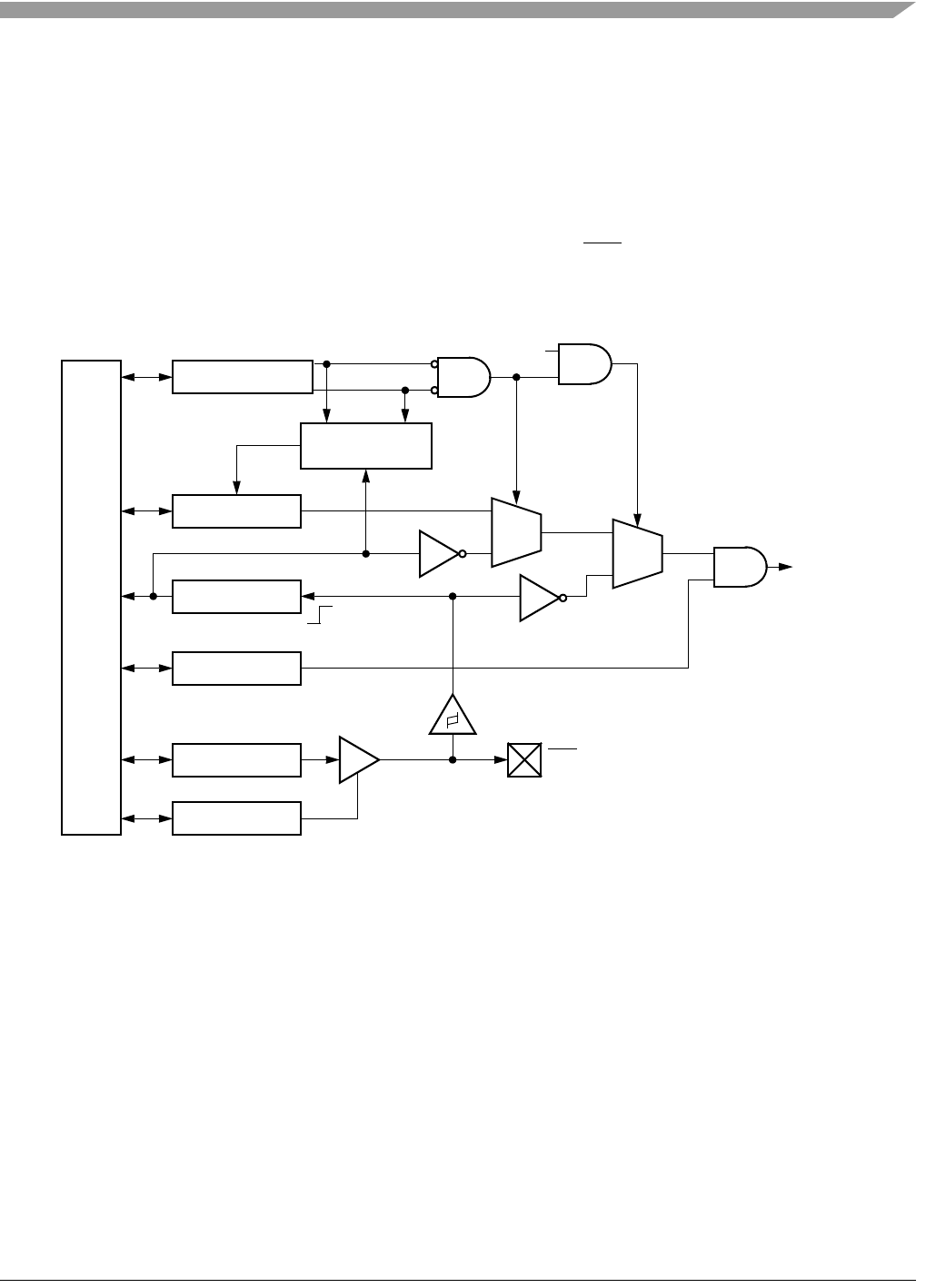
MCF548x Reference Manual, Rev. 3
Freescale Semiconductor 14-1
Chapter 14
Edge Port Module (EPORT)
14.1 Introduction
The edge port module (EPORT) has seven external interrupt pins, IRQ[7:1]. Each pin can be configured
individually as a level-sensitive interrupt pin, an edge-detecting interrupt pin (rising edge, falling edge, or
both), or a general-purpose input/output (I/O) pin. See Figure 14-1.
Figure 14-1. EPORT Block Diagram
14.2 Interrupt/General-Purpose I/O Pin Descriptions
All interrupt pins default to general-purpose input pins at reset. The pin value is synchronized to the rising
edge of the internal clock when read from the EPORT pin data register (EPPDR). The values used in the
edge/level detect logic are also synchronized to the rising edge of the internal clock. These pins use
Schmitt-triggered input buffers which have built-in hysteresis that decrease the probability of generating
false edge-triggered interrupts for slow rising and falling input signals.
When a pin is configured as an output, it is driven to a state whose level is determined by the corresponding
bit in the EPORT data register (EPDR). All bits in the EPDR are high at reset.
Internal Bus
Synchronizer
EPDRn
EPFRn
EPPAR[2n, 2n + 1]
EPIERn
Edge Detect
D0
Stop
Logic
EPPDRn
D1 QD0
D1 Q
Mode
EPDDRn
To Interrupt
Controller
IRQn PIN
Rising Edge
of System Clock

MCF548x Reference Manual, Rev. 3
14-2 Freescale Semiconductor
NOTE
The GPIO functionality of the external interrupt pins is controlled by the
EPORT module. However, some external interrupt signals are muxed with
other functions. In this case, the pin’s IRQ functionality must be enabled in
the GPIO module’s pin assignment register in order to use the pin’s GPIO
function via the EPORT registers. For more information, refer to
Chapter 15, “GPIO.”
14.3 Memory Map/Register Definition
This subsection describes the memory map and register structure.
14.3.1 Memory Map
Refer to Table 14-1 for a description of the EPORT memory map. The EPORT has an MBAR offset for
base address of 0xF00.
14.3.2 Register Descriptions
The EPORT programming model consists of these registers:
• The EPORT pin assignment register (EPPAR) controls the function of each pin individually.
• The EPORT data direction register (EPDDR) controls the direction of each pin individually.
• The EPORT interrupt enable register (EPIER) enables interrupt requests for each pin individually.
• The EPORT data register (EPDR) holds the data to be driven to the pins.
• The EPORT pin data register (EPPDR) reflects the current state of the pins.
• The EPORT flag register (EPFR) individually latches EPORT edge events.
Table 14-1. Edge Port Module Memory Map
MBAR
Offset Name Byte0 Byte1 Byte2 Byte3 Access1
1S = CPU supervisor mode access only. S/U = CPU supervisor or user mode access. User mode accesses to
supervisor only addresses have no effect and result in a cycle termination transfer error.
0xF00 EPORT pin assignment register EPPAR —2S
0xF04 EPORT data direction register
EPORT interrupt enable register
EPDDR EPIER —2
2Writing to reserved address locations has no effect, and reading returns 0s.
S/U
0xF08 EPORT data register
EPORT pin data register
EPDR EPPDR —2
0xF0C EPORT flag register EPFR —2
Memory Map/Register Definition
MCF548x Reference Manual, Rev. 3
Freescale Semiconductor 14-3
14.3.2.1 EPORT Pin Assignment Register (EPPAR)
14.3.2.2 EPORT Data Direction Register (EPDDR)
1514131211109876543210
R EPPA7 EPPA6 EPPA5 EPPA4 EPPA3 EPPA2 EPPA1 0 0
W
Reset0000000000000000
Reg
Addr
MBAR + 0xF00
Figure 14-2. EPORT Pin Assignment Register (EPPAR)
Table 14-2. EPPAR Field Descriptions
Bits Name Description
15–2 EPPAnEPORT pin assignment select fields. The read/write EPPAn fields configure EPORT pins for level
detection and rising and/or falling edge detection.
Pins configured as level-sensitive are inverted so that a logic 0 on the external pin represents a valid
interrupt request. Level-sensitive interrupt inputs are not latched. To guarantee that a level-sensitive
interrupt request is acknowledged, the interrupt source must keep the signal asserted until
acknowledged by software. Level sensitivity must be selected to bring the device out of stop mode
with an IRQn interrupt.
Pins configured as edge-triggered are latched and need not remain asserted for interrupt
generation. A pin configured for edge detection can trigger an interrupt regardless of its
configuration as input or output.
Interrupt requests generated in the EPORT module can be masked by the interrupt controller
module. EPPAR functionality is independent of the selected pin direction.
Reset clears the EPPAn fields.
00 Pin IRQn level-sensitive
01 Pin IRQn rising edge triggered
10 Pin IRQn falling edge triggered
11 Pin IRQn both falling edge and rising edge triggered
1–0 — Reserved, should be cleared.
76543210
R EPDD7 EPDD6 EPDD5 EPDD4 EPDD3 EPDD2 EPDD1 0
W
Reset00000000
Reg
Addr
MBAR + 0xF04
Figure 14-3. EPORT Data Direction Register (EPDDR)

MCF548x Reference Manual, Rev. 3
14-4 Freescale Semiconductor
14.3.2.3 Edge Port Interrupt Enable Register (EPIER)
14.3.2.4 Edge Port Data Register (EPDR)
Table 14-3. EPDDR Field Descriptions
Bits Name Description
7–1 EPDDnSetting any bit in the EPDDR configures the corresponding pin as an output. Clearing any bit in
EPDDR configures the corresponding pin as an input. Pin direction is independent of the level/edge
detection configuration. Reset clears EPDD7–EPDD1.
To use an EPORT pin as an external interrupt request source, its corresponding bit in EPDDR must
be clear. Software can generate interrupt requests by programming the EPORT data register when
the EPDDR selects output.
0 Corresponding EPORT pin configured as input
1 Corresponding EPORT pin configured as output
0 — Reserved, should be cleared.
76543210
R EPIE7 EPIE6 EPIE5 EPIE4 EPIE3 EPIE2 EPIE1 0
W
Reset00000000
Reg
Addr
MBAR + 0xF05
Figure 14-4. EPORT Port Interrupt Enable Register (EPIER)
Table 14-4. EPIER Field Descriptions
Bits Name Description
7–1 EPIEnEdge port interrupt enable bits enable EPORT interrupt requests. If a bit in EPIER is set, EPORT
generates an interrupt request when:
• The corresponding bit in the EPORT flag register (EPFR) is set or later becomes set.
• The corresponding pin level is low and the pin is configured for level-sensitive operation.
Clearing a bit in EPIER negates any interrupt request from the corresponding EPORT pin. Reset
clears EPIE7–EPIE1.
0 Interrupt requests from corresponding EPORT pin disabled
1 Interrupt requests from corresponding EPORT pin enabled
0 — Reserved, should be cleared.
76543210
R EPD7 EPD6 EPD5 EPD4 EPD3 EPD2 EPD1 0
W
Reset11111111
Reg
Addr
MBAR + 0xF08
Figure 14-5. EPORT Port Data Register (EPDR)

Memory Map/Register Definition
MCF548x Reference Manual, Rev. 3
Freescale Semiconductor 14-5
14.3.2.5 Edge Port Pin Data Register (EPPDR)
14.3.2.6 Edge Port Flag Register (EPFR)
Table 14-5. EPDR Field Descriptions
Bits Name Description
7–1 EPDx Edge port data bits. Data written to EPDR is stored in an internal register; if any pin of the port is
configured as an output, the bit stored for that pin is driven onto the pin. Reading EDPR returns
the data stored in the register. Reset sets EPD7-EPD1.
0 — Reserved, should be cleared.
76543210
R EPPD7 EPPD6 EPPD5 EPPD4 EPPD3 EPPD2 EPPD1 0
W
Reset Current pin state 0
Reg
Addr
MBAR + 0xF09
Figure 14-6. EPORT Port Pin Data Register (EPPDR)
Table 14-6. EPPDR Field Descriptions
Bits Name Description
7–1 EPPDx Edge port pin data bits. The read-only EPPDR reflects the current state of the EPORT pins
IRQ7–IRQ1. Writing to EPPDR has no effect, and the write cycle terminates normally. Reset does
not affect EPPDR.
0 — Reserved, should be cleared.
76543210
R EPF7 EPF6 EPF5 EPF4 EPF3 EPF2 EPF1 0
W
Reset00000000
Reg
Addr
MBAR + 0xF0C
Figure 14-7. EPORT Port Flag Register (EPFR)

MCF548x Reference Manual, Rev. 3
14-6 Freescale Semiconductor
Table 14-7. EPFR Field Descriptions
Bits Name Description
7–1 EPFnEdge port flag bits. When an EPORT pin is configured for edge triggering, its corresponding
read/write bit in EPFR indicates that the selected edge has been detected. Reset clears
EPF7–EPF1.
Bits in this register are set when the selected edge is detected on the corresponding pin. A bit
remains set until cleared by writing a 1 to it. Writing 0 has no effect. If a pin is configured as
level-sensitive (EPPARn= 00), pin transitions do not affect this register.
0 Selected edge for IRQx pin has not been detected.
1 Selected edge for IRQx pin has been detected.
0 — Reserved, should be cleared.

MCF548x Reference Manual, Rev. 3
Freescale Semiconductor 15-1
Chapter 15
GPIO
15.1 Introduction
Many of the MCF548x pins whose primary function is to serve as the external interface to off-chip
resources may also be used for general-purpose digital I/O (GPIO) access and for one or two secondary
functions. When used for GPIO purposes, the port x pins (PXXX) indicate which port is being accessed. In
some cases, the pin function is set by the operating mode, and the alternate pin functions are not supported.
The MCF548x GPIO signals are grouped into 8-bit ports; however, some ports do not use all eight bits.
Each GPIO port has registers that configure, monitor, and control the port signals.
Figure 15-1 is a block diagram of the MCF548x GPIO module.
NOTE
The actual signals and functions available vary for different members of the
MCF548x family. See Chapter 2, “Signal Descriptions,” for more details.
MCF548x Reference Manual, Rev. 3
15-2 Freescale Semiconductor
Figure 15-1. MCF548x GPIO Module Block Diagram
15.1.1 Overview
The MCF548x GPIO module controls the configuration and use for the following external GPIO ports
(register types in parentheses):
• ColdFire bus (FlexBus) accesses (FBCTL, FBCS)
DACK[1:0] / PDMA[3:2]
FBCS[5:1] / PFBCS[5:1]
BWE[3:0] / PFBCTL[7:4]
PORT
PORT
PORT
PORT
PORT
PORT
PORT
PORT
PORT
PORT
PORT
PSC3CTS / PPSC3PSC27
DSPISCK / PDSPI2
PORT
FBCTL
FBCS
DMA
FEC0H
FEC0L
FEC1H
FEC1L
PCIBG
PCIBR
PSC3PSC2
PSC1PSC0
DSPI
OE / PFBCTL3
TA / PFBCTL1
R/W / PFBCTL2
ALE / PFBCTL0
DREQ[1:0] / PDMA[1:0]
FEC0TXCLK / PFEC0H7
FEC0TXEN / PFEC0H6
FEC0TXD0 / PFEC0H5
FEC0COL / PFEC0H4
FEC0RXCLK / PFEC0H3
FEC0RXDV / PFEC0H2
FEC0RXD0 / PFEC0H1
FEC0CRS / PFEC0H0
FEC0TXD3 / PFEC0L7
FEC0TXD2 / PFEC0L6
FEC0TXD1 / PFEC0L5
FEC0TXER / PFEC0L4
FEC0RXD3 / PFEC0L3
FEC0RXD2 / PFEC0L2
FEC0RXD1 / PFEC0L1
FEC0RXER / PFEC0L0
FEC1TXCLK / PFEC1H7
FEC1TXEN / PFEC1H6
FEC1TXD0 / PFEC1H5
FEC1COL / PFEC1H4
FEC1RXCLK / PFEC1H3
FEC1RXDV / PFEC1H2
FEC1RXD0 / PFEC1H1
FEC1CRS / PFEC1H0
FEC1TXD3 / PFEC1L7
FEC1TXD2 / PFEC1L6
FEC1TXD1 / PFEC1L5
FEC1TXER / PFEC1L4
FEC1RXD3 / PFEC1L3
FEC1RXD2 / PFEC1L2
FEC1RXD1 / PFEC1L1
FEC1RXER / PFEC1L0
PCIBG[4:0] / PPCIBG[4:0]
PCIBR[4:0] / PPCIBR[4:0]
PSC3RTS / PPSC3PSC26
PSC3RXD / PPSC3PSC25
PSC3TXD / PPSC3PSC24
PSC2CTS / PPSC3PSC23
PSC2RTS / PPSC3PSC22
PSC2RXD / PPSC3PSC21
PSC2TXD / PPSC3PSC20
PSC1CTS / PPSC1PSC07
PSC1RTS / PPSC1PSC06
PSC1RXD / PPSC1PSC05
PSC1TXD / PPSC1PSC04
PSC0CTS / PPSC1PSC03
PSC0RTS / PPSC1PSC02
PSC0RXD / PPSC1PSC01
PSC0TXD / PPSC1PSC00
DSPISIN / PDSPI1
DSPISOUT / PDSPI1
DSPIPCS5 / PCSS / PDSPI6
DSPIPCS3 / PDSPI5
DSPIPCS2 / PDSPI4
DSPIPCS0 / SS / PDSPI3
PORT
FECI2C
FEC0EMDIO / PFECI2C3
FEC0EMDC / PFECI2C2
SCL / PFECI2C1
SDA / PFECI2C0
PORT
IRQ
1
PORT
TIM
2
IRQ[7:1] / PIRQ[5:1]
TOUT[3:0] / PTIM[7:4]
TIN[3:0] / PTIM[3:0]
1
The port IRQ GPIO functionality is provided through the EPORT module.
2
The port TIM GPIO funtionality is provided through the GPT module.

External Pin Description
MCF548x Reference Manual, Rev. 3
Freescale Semiconductor 15-3
• External DMA request and acknowledge (DMA)
• PCI bus access (PCIGNT, PCIREQ)
• Ethernet data and control (FEC0H, FEC0L, FEC1H, FEC1L, FECI2C)
•I
2C serial control (FECI2C)
• DMA serial peripheral interface (DSPI)
• Programmable serial control (PSC1PSC0 and PSC3PSC2)
15.1.2 Features
The MCF548x GPIO module includes these distinctive features:
• Control of primary function use of the supported GPIO ports indicated in Section 15.1.1,
“Overview”
• General purpose I/O support for all ports:
— Registers for storing output pin data
— Registers for controlling pin data direction
— Registers for reading current pin state
— Registers for setting and clearing output pin data registers
15.2 External Pin Description
The MCF548x GPIO module controls the functionality of several external pins. These pins are listed in
Table 15-1.
Table 15-1. MCF548x GPIO Module External Pins
Primary
Function
(Pin Name)1GPIO Alternate
Function 1
Alternate
Function 2 Description
Flexbus Control
BWE[3:2] PFBCTL[7:6] BE / BWE[3:2] TSIZ[1:0] Byte write strobes for external data transfer / Port
FBCTL[7:4] / Byte enables for external data transfer /
FlexBus transfer size
BWE[1:0] PFBCTL[5:4] BE / BWE[1:0] FBADDR[1:0] Byte write strobes for external data transfer / Port
FBCTL[7:4] / Byte enables for external data transfer /
FlexBus address[1:0]
OE PFBCTL3 — — Output enable for external reads / Port FBCTL3
R/W PFBCTL2 TBST — Read/write indication for external data transfer / Port
FBCTL2 / FlexBus transfer burst
TA PFBCTL1 — — Transfer acknowledge for external data transfer / Port
FBCTL1
ALE PFBCTL0 TBST — Address latch enable indication for external data transfer
/ Port FBCTL0 / FlexBus transfer burst
Flexbus Chip Selects
FBCS[5:1] PFBCS[5:1] — — Flexbus chip selects 5 – 1 / Port FBCS[5:4]
DMA Controller
DACK1 PDMA3 TOUT1 — DMA acknowledge 1 / Port DMA3 / GP timer output 1

MCF548x Reference Manual, Rev. 3
15-4 Freescale Semiconductor
DACK0 PDMA2 TOUT0 — DMA acknowledge 0 / Port DMA2 / GP timer output 0
DREQ1 PDMA1 TIN1 IRQ1 DMA request 1 / Port DMA1 / GP timer input 1 / Interrupt 1
DREQ0 PDMA0 TIN0 — DMA request 0 / Port DMA0 / GP timer input 0
Fast Ethernet Controller 0
FEC0TXCLK PFEC0H7 — — Ethernet Controller 0 transmit clock / Port FEC0H7
FEC0TXEN PFEC0H6 — — Ethernet Controller 0 transmit enable / PFEC0H6
FEC0TXD0 PFEC0H5 — — Ethernet Controller 0 transmit data 0 / Port FEC0H5
FEC0COL PFEC0H4 — — Ethernet Controller 0 collision / Port FEC0H4
FEC0RXCLK PFEC0H3 — — Ethernet Controller 0 receive clock / Port FEC0H3
FEC0RXDV PFEC0H2 — — Ethernet Controller 0 receive data valid / Port FEC0H2
FEC0RXD0 PFEC0H1 — — Ethernet Controller 0 receive data 0 / Port FEC0H1
FEC0CRS PFEC0H0 — — Ethernet Controller 0 carrier receive sense / Port FEC0H0
FEC0TXD[3:1] PFEC0L[7:5] — — Ethernet Controller 0 transmit data / Port FEC0L[7:5]
FEC0TXER PFEC0L4 — — Ethernet Controller 0 transmit error / Port FEC0L4
FEC0RXD[3:1] PFEC0L[3:1] — — Ethernet Controller 0 receive data [3:1] / Port FEC0L[3:1]
FEC0RXER PFEC0L0 — — Ethernet Controller 0 receive error / Port FEC0L0
FEC0MDIO PFECI2C3 — — Ethernet Controller 0 management data control / Port
FECI2C3
FEC0MDC PFECI2C2 — — Ethernet Controller 0 management data clock / Port
FECI2C2
Fast Ethernet Controller 1
FEC1TXCLK PFEC1H7 — — Ethernet Controller 1 transmit clock / Port FEC1H7
FEC1TXEN PFEC1H6 — — Ethernet Controller 1 transmit enable / Port FEC1H6
FEC1TXD0 PFEC1H5 — — Ethernet Controller 1 transmit data 0 / Port FEC1H5
FEC1COL PFEC1H4 — — Ethernet Controller 1 collision / Port FEC1H4
FEC1RXCLK PFEC1H3 — — Ethernet Controller 1 receive clock / Port FEC1H3
FEC1RXDV PFEC1H2 — — Ethernet Controller 1 receive data valid / Port FEC1H2
FEC1RXD0 PFEC1H1 — — Ethernet Controller 1 receive data 0 / Port FEC1H1
FEC1CRS PFEC1H0 — — Ethernet Controller 1 carrier receive sense / Port FEC1H0
FEC1TXD[3:1] PFEC1L[7:5] — — Ethernet Controller 1 transmit data / Port FEC1L[7:5]
FEC1TXER PFEC1L4 — — Ethernet Controller 1 transmit error / Port FEC1L4
FEC1RXD[3:1] PFEC1L[3:1] — — Ethernet Controller 1 receive data [3:1] / Port FEC1L[3:1]
FEC1RXER PFEC1L0 — — Ethernet Controller 1 receive error / Port FEC1L0
FEC1MDIO — SDA CANRX0 Ethernet Controller 1 management data control / I2C
serial data / FlexCAN 0 receive data
Table 15-1. MCF548x GPIO Module External Pins (Continued)
Primary
Function
(Pin Name)1GPIO Alternate
Function 1
Alternate
Function 2 Description

External Pin Description
MCF548x Reference Manual, Rev. 3
Freescale Semiconductor 15-5
FEC1MDC — SCL CANTX0 Ethernet Controller 1 management data clock / I2C serial
clock / FlexCAN 0 transmit data
I2C Serial Control
SDA PFECI2C1 ——I2C serial data / Port FECI2C1
SCL PFECI2C0 ——I2C serial clock / Port FECI2C0
External Interrupts
IRQ6 PIRQ62CANRX1 — Interrupt 6 / Port IRQ6 / FlexCAN 1 receive data
IRQ5 PIRQ52CANRX1 — Interrupt 5 / Port IRQ5 / FlexCAN 1 receive data
DMA Serial Peripheral Interface
DSPICS5/PCSS PDSPI6 — — DSPI synchronous peripheral chip select 3 / Port DSPI6
DSPICS3 PDSPI5 TOUT3 CANTX1 DSPI synchronous peripheral chip select 3 / Port DSPI5 /
GP timer out 3 / FlexCAN 1 transmit data
DSPICS2 PDSPI4 TOUT2 CANTX1 DSPI synchronous peripheral chip select 3 / Port DSPI4 /
GP timer out 2 / FlexCAN 1 transmit data
DSPICS0/SS PDSPI3 PSC3RTS PSC3FSYNC DSPI synchronous peripheral chip select 3 / Port DSPI3 /
PSC3 request-to-send / PSC3 frame sync
DSPISCK PDSPI2 PSC3CTS PSC3BCLK DSPI serial clock / Port DSPI2 / PSC3 clear-to-send /
PSC3 modem clock
DSPISIN PDSPI1 PSC3RXD — DSPI serial data input / Port DSPI1 / PSC3 receive data
DSPISOUT PDSPI0 PSC3TXD — DSPI serial data output / Port DSPI 0 / PSC3 transmit data
Programmable Serial Control Module 3
PSC3CTS PPSC3PSC27 PSC3BCLK — PSC3 clear-to-send indication / Port PSC3PSC27 / PSC3
modem clock
PSC3RTS PPSC3PSC26 PSC3FSYNC — PSC3 request-to-send indication / Port PSC3PSC26 /
PSC3 frame sync
PSC3RXD PPSC3PSC25 — — PSC3 receive data / Port PSC3PSC25
PSC3TXD PPSC3PSC24 — — PSC3 transmit data / Port PSC3PSC24
Programmable Serial Control Module 2
PSC2CTS PPSC3PSC23 PSC2BCLK CANRX0 PSC2 clear-to-send indication / Port PSC3PSC23 / PSC2
modem clock
PSC2RTS PPSC3PSC22 PSC2FSYNC CANTX0 PSC2 request-to-send indication / Port PSC3PSC22 /
PSC2 frame sync
PSC2RXD PPSC3PSC21 — — PSC2 receive data / Port PSC3PSC21
PSC2TXD PPSC3PSC20 — — PSC2 transmit data / Port PSC3PSC20
Programmable Serial Control Module 1
PSC1CTS PPSC1PSC07 PSC1BCLK — PSC1 clear-to-send indication / Port PSC1PSC07 / PSC1
modem clock
Table 15-1. MCF548x GPIO Module External Pins (Continued)
Primary
Function
(Pin Name)1GPIO Alternate
Function 1
Alternate
Function 2 Description

MCF548x Reference Manual, Rev. 3
15-6 Freescale Semiconductor
Refer to the signals chapter of the MCF548x chip specification for more detailed descriptions of these
signals. The function of most of the pins (primary function, GPIO, etc.) is determined by the GPIO module
pin assignment registers.
PSC1RTS PPSC1PSC06 PSC1FSYNC — PSC1 request-to-send indication / Port PSC1PSC06 /
PSC1 frame sync
PSC1RXD PPSC1PSC05 — — PSC1 receive data / Port PSC1PSC05
PSC1TXD PPSC1PSC04 — — PSC1 transmit data / Port PSC1PSC04
Programmable Serial Control Module 0
PSC0CTS PPSC1PSC03 PSC0BCLK — PSC0 clear-to-send indication / Port PSC1PSC03 / PSC0
modem clock
PSC0RTS PPSC1PSC02 PSC0FSYNC — PSC0 request-to-send indication / Port PSC1PSC02 /
PSC0 frame sync
PSC0RXD PPSC1PSC01 — — PSC0 receive data / Port PSC1PSC01
PSC0TXD PPSC1PSC00 — — PSC0 transmit data / Port PSC1PSC00
Peripheral Component Interface
PCIBG4 PPCIGNT4 TBST — PCI bus grant 4 / Port PCIGNT4 / Flexbus transfer burst
PCIBG3 PPCIGNT3 TOUT3 — PCI bus grant 3 / Port PCIGNT3 / GP timer out 3
PCIBG2 PPCIGNT2 TOUT2 — PCI bus grant 2 / Port PCIGNT2 / GP timer out 2
PCIBG1 PPCIGNT1 TOUT1 — PCI bus grant 1 / Port PCIGNT1 / GP timer out 1
PCIBG0 PPCIGNT0 TOUT0 — PCI bus grant 0 / Port PCIGNT0 / GP timer out 0
PCIBR4 PPCIREQ4 IRQ4 — PCI bus request 4 / Port PCIREQ4 / Interrupt 4
PCIBR3 PPCIREQ3 TIN2 — PCI bus request 3 / Port PCIREQ3 / GP timer in 3
PCIBR2 PPCIREQ2 TIN2 — PCI bus request 2 / Port PCIREQ2 / GP timer in 2
PCIBR1 PPCIREQ1 TIN1 — PCI bus request 1 / Port PCIREQ1 / GP timer in 1
PCIBR0 PPCIREQ0 TIN0 — PCI bus request 0 / Port PCIREQ0 / GP timer in 0
General Purpose Timer
TIN3 PTIM32IRQ3 CANRX1 GP timer in 3 / Port TIM7 / Interrupt 3 / FlexCAN 1 receive
data
TOUT3 PTIM72CANTX1 — GP timer out 3 / Port TIM6 / FlexCAN 1 transmit data
TIN2 PTIM22IRQ2 CANRX1 GP timer in 2 / Port TIM5 / Interrupt 1 / FlexCAN 2 receive
data
TOUT2 PTIM62CANTX1 — GP timer out 2 / Port TIM4 / FlexCAN 1 transmit data
1The primary functionality of a pin is not necessarily the default function of the pin after reset. Most pins that have muxed GPIO
functionality will default to GPIO inputs. See the reset value of the associated pin assignment register. See Section 15.3.2.5, “Port
x Pin Assignment Registers (PAR_x)”) for more information on default pin functionality.
2GPIO is supported, but the GPIO functionality is controlled by the timer or EPORT module instead of the GPIO module. Signals
are listed because there are pin assignment registers in the GPIO module for controlling the signal functions.
Table 15-1. MCF548x GPIO Module External Pins (Continued)
Primary
Function
(Pin Name)1GPIO Alternate
Function 1
Alternate
Function 2 Description

Memory Map/Register Definition
MCF548x Reference Manual, Rev. 3
Freescale Semiconductor 15-7
It should be noted from Table 15-1 that there are several cases where a function is mapped to more than
one pin. While it is possible to enable the function on more than one pin simultaneously, this type of
programming should be avoided for input functions to prevent unexpected behavior. All multiple-pin
functions are listed in Table 15-2.
15.3 Memory Map/Register Definition
15.3.1 Register Overview
Table 15-3 summarizes all the registers in the MCF548x GPIO module address space.
Table 15-2. MCF548x Multiple-Pin Functions
Function Direction Associated Pins
GP timer in 3 (TIN3) I TIN3, PCIBR3
GP timer in 2 (TIN2) I TIN2, PCIBR2
GP timer in 1 (TIN1) I TIN1, PCIBR1, DREQ1
GP timer in 0 (TIN0) I TIN0, PCIBR0, DMA_REQ0
GP timer out 3 (TOUT3) O TOUT3, PCIBG3, DSPI_PSC3
GP timer out 2 (T2OUT) O TOUT2, PCIBG2, DSPI_PSC2
GP timer out 1 (T1OUT) O TOUT1, PCIBG1, DACK1
GP timer out 0 (T0OUT) O TOUT0, PCIBG0, DACK0
FlexCAN 0 transmit data (CANTX0) O PSC2RTS, FEC1MDC
FlexCAN 0 receive data (CANRX0) I PSC2CTS, FEC1MDIO
FlexCAN 1 transmit data (CANTX1) O T3OUT, T2OUT, DSPI_PCS3, DSPI_PCS2
FlexCAN 1 receive data (CANRX1) I T3IN, T2IN, IRQ6, IRQ5
I2C serial data (SDA) I/O SDA, FEC1MDC
I2C serial clock (SCL) I/O SDA, FEC1MDIO
PSC3 request-to-send (PSC3RTS) O PSC3RTS, DSPIPCS0/SS
PSC3 clear-to-send (PSC3CTS) I PSC3CTS, DSPISCK
PSC3 modem clock (PSC3BCLK) I PSC3CTS, DSPISCK
PSC3 frame sync (PSC3FSYNC) I PSC3CTS, DSPIPCS0/SS
PSC3 uart receive data (PSC3RXD) I PSC3RXD, DSPISIN
PSC3 uart transmit data (PSC3TXD) O PSC3TXD, DSPISOUT
Table 15-3. MCF548x GPIO Module Memory Map
MBAR
Offset 31–24 23–16 15–8 7–0 Access1
Port Output Data Registers
0xA00 PODR_FBCTL PODR_FBCS PODR_DMA Reserved3S/U
0xA04 PODR_FEC0H PODR_FEC0L PODR_FEC1H PODR_FEC1L S/U

MCF548x Reference Manual, Rev. 3
15-8 Freescale Semiconductor
15.3.2 Register Descriptions
15.3.2.1 Port x Output Data Registers (PODR_x)
The PODR registers store the data to be driven on the corresponding port x pins when the pins are
configured for general purpose output.
0xA08 PODR_FECI2C PODR_PCIBG PODR_PCIBR Reserved3S/U
0xA0C PODR_PSC3PSC2 PODR_PSC1PSC0 PODR_DSPI Reserved3S/U
Port Data Direction Registers
0xA10 PDDR_FBCTL PDDR_FBCS PDDR_DMA Reserved2S/U
0xA14 PDDR_FEC0H PDDR_FEC0L PDDR_FEC1H PDDR_FEC1L S/U
0xA18 PDDR_FECI2C PDDR_PCIBG PDDR_PCIBR Reserved3S/U
0xA1C PDDR_PSC3PSC2 PDDR_PSC1PSC0 PDDR_DSPI Reserved3S/U
Port Pin Data/Set Data Registers
0xA20 PPDSDR_FBCTL PPDSDR_FBCS PPDSDR_DMA Reserved3S/U
0xA24 PPDSDR_FEC0H PPDSDR_FEC0L PPDSDR_FEC1H PPDSDR_FEC1L S/U
0xA28 PPDSDR_FECI2C PPDSDR_PCIBG PPDSDR_PCIBR Reserved3S/U
0xA2C PPDSDR_PSC3PSC2 PPDSDR_PSC1PSC0 PPDSDR_DSPI Reserved3S/U
Port Clear Output Data Registers
0xA30 PCLRR_FBCTL PCLRR_FBCS PCLRR_DMA Reserved3S/U
0xA34 PCLRR_FEC0H PCLRR_FEC0L PCLRR_FEC1H PCLRR_FEC1L S/U
0xA38 PCLRR_FECI2C PCLRR_PCIBG PCLRR_PCIBR Reserved3S/U
0xA3C PCLRR_PSC3PSC2 PCLRR_PSC1PSC0 PCLRR_DSPI Reserved3S/U
Pin Assignment Registers
0xA40 PAR_FBCTL PAR_FBCS PAR_DMA S/U
0xA44 PAR_FECI2CIRQ Reserved3S/U
0xA48 PAR_PCIBG PAR_PCIBR S/U
0xA4C PAR_PSC3 PAR_PSC2 PAR_PSC1 PAR_PSC0 S/U
0xA50 PAR_DSPI PAR_TIMER Reserved3S/U
0xA54–
0xA7F
Reserved3
1S/U = supervisor or user mode access.
2Reads to reserved locations return 0s. Writes have no effect.
Table 15-3. MCF548x GPIO Module Memory Map (Continued)
MBAR
Offset 31–24 23–16 15–8 7–0 Access1

Memory Map/Register Definition
MCF548x Reference Manual, Rev. 3
Freescale Semiconductor 15-9
Most PODR_x registers have full 8-bit implementations, as shown in Figure 15-2. The remaining PODR_x
registers use fewer than eight bits. These registers are shown in Figure 15-3, Figure 15-4, Figure 15-5, and
Figure 15-6.
The PODR_x registers are read/write. At reset, all implemented bits in the PODR_x registers are set.
Unimplemented bits always remain cleared.
Reading a PODR_x register returns the current values in the register, not the port x pin values.
To set bits in a PODR_x register, write 1s to the PODR_x bits, or write 1s to the corresponding bits in the
PORTP_x/SET_x register. To clear bits in a PODR_x register, write 0s to the PODR_x bits, or write 0s to
the corresponding bits in the PCLRR_x register.
15.3.2.1.1 8-Bit PODR_x Registers
The 8-bit PODR_x registers include the following:
• PODR_FBCTL
•PODR_FEC0H
•PODR_FEC0L
•PODR_FEC1H
•PODR_FEC1L
• PODR_PSC3PSC2
• PODR_PSC1PSC0
Figure 15-2 displays the 8-bit PODR_x registers.
15.3.2.1.2 7-Bit PODR_x Register
The 7-bit PODR_DSPI register is the output data register for the PDSPIn port. Figure 15-3 displays the
7-bit PODR_x register.
76543210
R PODRx7 PODRx6 PODRx5 PODRx4 PODRx3 PODRx2 PODRx1 PODRx0
W
Reset 1 1 1 1 1 1 1 1
Reg
Addr
MBAR + 0xA00 (PODR_FBCTL), 0xA04 (PODR_FEC0H), 0xA05 (PODR_FEC0L), 0xA06 (PODR_FEC1H),
0xA07 (PODR_FEC1L), 0xA0C (PODR_PSC3PSC2), 0xA0D (PODR_PSC1PSC0)
Figure 15-2. 8-Bit Port Output Data Registers (PODR_x)
Table 15-4. 8-Bit PODR_x Field Descriptions
Bits Name Description
7–0 PODRxnPODRx Output Data Bits
0 Drive 0 when PORT x pin is general purpose output
1 Drive 1 when PORT x pin is general purpose output

MCF548x Reference Manual, Rev. 3
15-10 Freescale Semiconductor
15.3.2.1.3 5-Bit PODR_x Registers
The 5-bit PODR_x registers are the output data registers for PPCIBGn (PODR_PCIBG) and PPCIBRn
(PODR_PCIBR). Figure 15-4 displays the 5-bit PODR_x registers.
15.3.2.1.4 4-Bit PODR_x Registers
The 4-bit PODR_x registers are the output data registers for PDMAn (PODR_DMA) and PFECI2Cn
(PODR_FECI2C). Figure 15-3 displays the 4-bit PODR_x registers.
76543210
R 0 PODRDSPI6 PODRDSPI5 PODRDSPI4 PODRDSPI3 PODRDSPI2 PODRDSPI1 PODRDSPI0
W
Reset01111111
Reg
Addr
MBAR + 0xA0E (PODR_DSPI)
Figure 15-3. 7-Bit PODR_DSPI Register (PODR_x)
Table 15-5. 7-Bit PODR_DSPI Field Descriptions
Bits Name Description
7 — Reserved, should be cleared
6–0 PODRDSPInPODR DSPI output data bits
0 Drive 0 when PDSPIn pin is general purpose output
1 Drive 1 when PDSPIn pin is general purpose output
76543210
R 0 0 0 PODRx4 PODRx3 PODRx2 PODRx1 PODRx0
W
Reset 00011111
Reg
Addr
MBAR + 0xA09 (PODR_PCIBG), 0xA0A (PODR_PCIBR)
Figure 15-4. 5-Bit PODR_PCIBG and PODR_PCIBR Registers
Table 15-6. 5-Bit PODR_PCIBG and PODR_PCIBR Field Descriptions
Bits Name Description
7–5 — Reserved, should be cleared
4–0 PODRxnPODR_PCIBG and PODR_PCIBR output data bits
0 Drive 0 when PPCIBGn or PPCIBRn pin is general purpose output
1 Drive 1 when PPCIBGn or PPCIBRn pin is general purpose output

Memory Map/Register Definition
MCF548x Reference Manual, Rev. 3
Freescale Semiconductor 15-11
15.3.2.1.5 FBCS Register (PODR_FBCS)
The 5-bit PODR_FBCS register is the output data register for PFBCSn (PODR_FBCS). Figure 15-6
displays the 5-bit PODR_FBCS register.
15.3.2.2 Port x Data Direction Registers (PDDR_x)
The PDDR registers control the direction of the port x pin drivers when the pins are configured for general
purpose I/O.
76543210
R 0 0 0 0 PODRx3 PODRx2 PODRx1 PODRx0
W
Reset00001111
Reg
Addr
MBAR + 0xA02 (PORT_DMA), 0xA08 (PORT_FECI2C)
Figure 15-5. 4-Bit PODR_DMA and PODR_FECI2C Registers
Table 15-7. 4-Bit PODR_DMA and PODR_FECI2C Field Descriptions
Bits Name Description
7–4 — Reserved, should be cleared
3–0 PODRxnPORT_DMA and PORT_FECI2C output data bits
0 Drive 0 when PDMAn or PFECI2Cn pin is general purpose output
1 Drive 1 when PDMAn or PFECI2Cn pin is general purpose output
76543210
R 0 0 PODRFB5 PODRFB4 PODRFB3 PODRFB2 PODRFB1 0
W
Reset00000000
Reg
Addr
MBAR + 0xA01 (PODR_FBCS)
Figure 15-6. 5-Bit PODR_FBCS Register
Table 15-8. 5-Bit PODR_FBCS Field Descriptions
Bits Name Description
7–6 — Reserved, should be cleared
5–1 PODRFBn PORT_FBCS output data
0 Drive 0 when PFBCSn pin is general purpose output
1 Drive 1 when PFBCSn pin is general purpose output
0 — Reserved, should be cleared

MCF548x Reference Manual, Rev. 3
15-12 Freescale Semiconductor
Most PDDR_x registers have a full 8-bit implementation, as shown in Figure 15-7. The remaining
PDDR_x registers use fewer than eight bits. Their bit definitions are shown in Figure 15-8, Figure 15-9,
Figure 15-10, and Figure 15-11.
The PDDR_x registers are read/write. At reset, all bits in the PDDR_x registers are cleared. Setting any bit
in a PDDR_x register configures the corresponding port x pin as an output. Clearing any bit in a PDDR_x
register configures the corresponding pin as an input.
15.3.2.2.1 8-Bit PDDR_x Registers
The 8-bit PDDR_x registers include the following:
• PDDR_FBCTL
•PDDR_FEC0H
•PDDR_FEC0L
•PDDR_FEC1H
•PDDR_FEC1L
• PDDR_PSC3PSC2
• PDDR_PSC1PSC0
Figure 15-7 displays the 8-bit PDDR_x registers.
15.3.2.2.2 7-Bit PDDR_x Register
The 7-bit PDDR_DSPI register sets the data direction for the PDSPIn port. Figure 15-8 displays the 7-bit
PDDR_DSPI register.
76543210
RDDx7DDx6DDx5DDx4DDx3DDx2DDx1DDx0
W
Reset00000000
Reg
Addr
MBAR + 0xA10 (PDDR_FBCTL), 0xA14 (PDDR_FEC0H), 0xA15 (PDDR_FEC0L), 0xA16 (PDDR_FEC1H), 0xA17
(PDDR_FEC1L), 0xA1C (PDDR_PSC3PSC2), 0xA1D (PDDR_PSC1PSC0)
Figure 15-7. 8-Bit Port Data Direction Registers
Table 15-9. 8-Bit PDDR_x Field Descriptions
Bits Name Description
7–0 DDxn PDDR_x Data Direction Bits
0PORT x pin is configured as input
1PORT x pin is configured as output

Memory Map/Register Definition
MCF548x Reference Manual, Rev. 3
Freescale Semiconductor 15-13
15.3.2.2.3 5-Bit PDDR_x Registers
The 5-bit PDDR_x registers are the data direction registers for PPCIBGn (PDDR_PCIBG) and PPCIBRn
(PDDR_PCIBR). Figure 15-9 displays the 5-bit PDDR_x registers.
15.3.2.2.4 4-Bit PDDR_x Registers
The 4-bit PDDR_x registers are for data direction of PDMAn (PDDR_DMA) and PFECI2Cn
(PDDR_FECI2C). Figure 15-10 displays the 4-bit PDDR_x registers.
76543210
R 0 DDDSP
6
DDDSP5 DDDSP4 DDDSPI3 DDDSPI2 DDDSP1 DDDSP0
W
Reset00000000
Reg
Addr
MBAR + 0xA1E (PDDR_DSPI)
Figure 15-8. 7-Bit PDDR_DSPI Data Direction Register
Table 15-10. 7-Bit PDDR_DSPI Field Descriptions
Bits Name Description
7 — Reserved, should be cleared
6–0 DDDSPnPODR_DSPI data direction
0 PDSPIn pin configured as input
1 PDSPIn pin configured as output
76543210
R0 0 0 DDx4DDx3DDx2DDx1DDx0
W
Reset00000000
Reg
Addr
MBAR + 0xA11 (PDDR_FBCS), 0xA19 (PDDR_PCIBG), 0xA1A (PDDR_PCIBR)
Figure 15-9. 5-Bit PDDR_PCIBG and PDDR_PCIBR Registers
Table 15-11. 5-Bit PDDR_PCIBG and PDDR_PCIBR Field Descriptions
Bits Name Description
7–5 — Reserved, should be cleared
4–0 DDxn PDDR_PCIBG and PDDR_PCIBR Data Direction
0 PPCIBGn or PPCIBRn pin is configured as input
1 PPCIBGn or PPCIBRn pin is configured as output

MCF548x Reference Manual, Rev. 3
15-14 Freescale Semiconductor
15.3.2.2.5 FBCS Register (PDDR_FBCS)
The 5-bit PDDR_FBCS register is for data direction of PFBCSn. Figure 15-11 displays the 5-bit
PDDR_FBCS register.
15.3.2.3 Port x Pin Data/Set Data Registers (PPDSDR_x)
The PPDSDR registers reflect the current pin states and control the setting of output pins when the pin is
configured for general purpose I/O.
76543210
R0 0 0 0 DDx3DDx2DDx1DDx0
W
Reset00000000
Reg
Addr
MBAR + 0xA12 (PDDR_DMA), 0xA18 (PDDR_FECI2C)
Figure 15-10. 4-Bit PDDR_DMA and PDDR_FECI2C Registers
Table 15-12. 4-Bit PDDR_DMA and PDDR_FECI2C Field Descriptions
Bits Name Description
7–4 — Reserved, should be cleared
3–0 DDxn PDDR_DMA and PDDR_FECI2C Data Direction
0PDMAn or PFECI2Cn pin is configured as input
1PDMAn or PFECI2Cn pin is configured as output
76543210
R 0 0 DDFB5 DDFB4 DDFB3 DDFB2 DDFB1 0
W
Reset00000000
Reg
Addr
MBAR + 0xA11 (PDDR_FBCS)
Figure 15-11. 5-Bit PDDR_FBCS Register
Table 15-13. 5-Bit PDDR_FBCS Field Descriptions
Bits Name Description
7–6 — Reserved, should be cleared
5–1 DDFBnPDDR_FBCS data direction
0PFBCSn pin is configured as input
1PFBCSn pin is configured as output
0 — Reserved, should be cleared

Memory Map/Register Definition
MCF548x Reference Manual, Rev. 3
Freescale Semiconductor 15-15
Most PPDSDR_x registers have a full 8-bit implementation, as shown in Figure 15-12. The remaining
PPDSDR_x registers use fewer than eight bits. Their bit definitions are shown in Figure 15-13,
Figure 15-14, Figure 15-15, and Figure 15-16.
The PPDSDR_x registers are read/write. At reset, the bits in the PPDSDR_x registers are set to the current
pin states. Reading a PPDSDR_x register returns the current state of the port x pins. Writing 1s to a
PPDSDR_x register sets the corresponding bits in the PODR_x register. Writing 0s has no effect.
15.3.2.3.1 8-Bit PPDSDR_x Registers
The 8-bit PPDSDR_x registers include the following:
• PPDSDR_FBCTL
• PPDSDR_FEC0H
• PPDSDR_FEC0L
• PPDSDR_FEC1H
• PPDSDR_FEC1L
• PPDSDR_PSC3PSC2
• PPDSDR_PSC1PSC0
• PPDSDR_PSC3PSC2
Figure 15-12 displays the 8-bit PPDSDR_x registers.
15.3.2.3.2 7-Bit PPDSDR_x Register
The 7-bit PPDSDR_x register is for pin data and set data for PDSPIn. Figure 15-13 displays the 7-bit
PPDSDR_DSPI register.
76543210
R PPDx7 PPDx6 PPDx5 PPDx4 PPDx3 PPDx2 PPDx1 PPDx0
W PSDx7 PSDx6 PSDx5 PSDx4 PSDx3 PSDx2 PSDx1 PSDx0
Reset P1P1P1P1P1P1P1P1
Reg
Addr
MBAR + 0xA20 (PPDSDR_FBCTL), 0xA24 (PPDSDR_FEC0H), 0xA25 (PPDSDR_FEC0L), 0xA26
(PPDSDR_FEC1H), 0xA27 (PPDSDR_FEC1L), 0xA2C (PPDSDR_PSC3PSC2), 0xA2D (PPDSDR_PSC1PSC0)
1P = the current pin state. The exception is that PPDSDR_FBCTL is always reset to 0.
Figure 15-12. 8-Bit Port Pin Data / Set Data Registers
Table 15-14. 8-Bit PPDSDR_x Field Descriptions
Bits Name Description
7–0 PPDxnPort pin data. This is read-only.
0Port x pin state is low
1Port x pin state is high
PSDxnPort set data.
0 No effect
1 Corresponding PODR_x bit is set

MCF548x Reference Manual, Rev. 3
15-16 Freescale Semiconductor
15.3.2.3.3 5-Bit PPDSDR_x Registers
The 5-bit PPDSDR_x registers are the pin data and set data registers for PPCIBGn (PPDSDR_PCIBG) and
PPCIBRn (PPDSDR_PCIBR). Figure 15-14 displays the 5-bit PPDSDR_x registers.
76543210
R 0 PPDx6 PPDx5 PPDx4 PPDx3 PPDx2 PPDx1 PPDx0
WPSDx6 PSDx5 PSDx4 PSDx3 PSDx2 PSDx1 PSDx0
Reset 0 P1P1P1P1P1P1P1
Reg
Addr
MBAR + 0xA2E (PPDSDR_DSPI)
1P = the current pin state.
Figure 15-13. 7-Bit Port Pin Data / Set Data Registers
Table 15-15. 7-Bit PPDSDR_DSPI Field Descriptions
Bits Name Description
7 — Reserved, should be cleared.
6–0 PPDxnPPDSDR_DSPI pin data. This is Read-only.
0 PDSPIn pin state is low
1 PDSPIn pin state is high
PSDxnPPDSDR_DSPI set data.
0 No effect
1 Corresponding PODR_DSPI bit is set
76543210
R 0 0 0 PPDx4 PPDx3 PPDx2 PPDx1 PPDx0
W PSDx4 PSDx3 PSDx2 PSDx1 PSDx0
Reset000P
1P1P1P1P1
Reg
Addr
MBAR + 0xA29 (PPDSDR_PCIBG) and 0xA2A (PPDSDR_PCIBR)
1P = the current pin state.
Figure 15-14. 5-Bit PPDSDR_PCIBG and PPDSDR_PCIBR Registers
Table 15-16. 5-Bit PPDSDR_PCIBG and PPDSDR_PCIBR Field Descriptions
Bits Name Description
7–5 — Reserved, should be cleared.

Memory Map/Register Definition
MCF548x Reference Manual, Rev. 3
Freescale Semiconductor 15-17
15.3.2.3.4 4-Bit PPDSDR_x Registers
The 4-bit PPDSDR_x registers are the pin data and set data registers for PDMAn (PPDSDR_DMA) and
PFECI2Cn (PPDSDR_FECI2C). Figure 15-15 displays the 4-bit PPDSDR_DMA and PPDSDR_FECI2C
registers.
15.3.2.3.5 FBCS Register (PPDSDR_FBCS)
The 5-bit PPDSDR_FBCS register is for pin data and set data for PFBCSn. Figure 15-16 displays the 5-bit
PPDSDR_FBCS register.
4–0 PPDxnPPDSDR_PCIBG and PPDSDR_PCIBR pin data. This is Read-only.
0 PPCIBGn or PPCIBRn pin state is low
1 PPCIBGn or PPCIBRn pin state is high
PSDxnPPDSDR_PCIBG and PPDSDR_PCIBR set data.
0 No effect
1 Corresponding PODR_PCIBGn or PODR_PCIBRn bit is set
76543210
R 0 0 0 0 PPDx3 PPDx2 PPDx1 PPDx0
WPSDx3 PSDx2 PSDx1 PSDx0
Reset 0 0 0 0 P1P1P1P1
Reg
Addr
MBAR + 0xA22 (PPDSDR_DMA) and 0xA28 (PPDSDR_FECI2C)
1P = the current pin state.
Figure 15-15. 4-Bit PPDSDR_DMA and PPDSDR_FECI2C Registers
Table 15-17. 4-Bit PPDSDR_DMA and PPDSDR_FECI2C Field Descriptions
Bits Name Description
7–4 — Reserved, should be cleared.
4–0 PPDxnPPDSDR_DMA and PPDSDR_FECI2C pin data. This is Read-only.
0PDMAn or PFECI2Cn pin state is low
1PDMAn or PFECI2Cn pin state is high
PSDXnPPDSDR_DMA and PPDSDR_FECI2C set data.
0 No effect
1 Corresponding PODR_DMA or PODR_FECI2C bit is set
Table 15-16. 5-Bit PPDSDR_PCIBG and PPDSDR_PCIBR Field Descriptions (Continued)
Bits Name Description

MCF548x Reference Manual, Rev. 3
15-18 Freescale Semiconductor
15.3.2.4 Port x Clear Output Data Registers (PCLRR_x)
Writing 0s to a PCLRR_x register clears the corresponding bits in the PODR_x register. Writing 1s has no
effect. Reading the PCLRR_x register returns 0s.
Most PCLRR_x registers have a full 8-bit implementation, as shown in Figure 15-17. The remaining
PCLRR_x registers use fewer than eight bits. Their bit definitions are shown in Figure 15-18,
Figure 15-19, Figure 15-20, and Figure 15-21.
The PCLRR_x registers are read/write. The 8-bit PCLRR_x registers include the following:
• PCLRR_FBCTL
• PCLRR_FEC0H
• PCLRR_FEC0L
• PCLRR_FEC1H
• PCLRR_FEC1L
• PCLRR_PSC3PSC2
• PCLRR_PSC1PSC0
Figure 15-17 displays the 8-bit PCLRR_x registers.
76543210
R 0 0 PPDx5 PPDx4 PPDx3 PPDx2 PPDx1 0
WPSDx5 PSDx4 PSDx3 PSDx2 PSDx1
Reset 0 0 P1P1P1P1P10
Reg
Addr
MBAR + 0xA21 (PDDSDR_FBCS)
1P = the current pin state.
Figure 15-16. 5-Bit PDDSDR_FBCS Register
Table 15-18. 5-Bit PDDSDR_FBCS Field Descriptions
Bits Name Description
7–6 — Reserved, should be cleared.
5–1 PPDxnPDDSDR_FBCS pin data. This is Read-only.
0PFBCSn pin state is low
1PFBCSn pin state is high
PSDxnPDDSDR_FBCS set data.
0 No effect
1 Corresponding PODR_FBCS bit is set
0 — Reserved, should be cleared.

Memory Map/Register Definition
MCF548x Reference Manual, Rev. 3
Freescale Semiconductor 15-19
15.3.2.4.1 7-Bit PCLRR_x Register
The 7-bit PCLRR_DSPI register is the clear output data register for PDSPIn. Figure 15-18 displays the
7-bit PCLRR_DSPI register.
15.3.2.4.2 5-Bit PCLRR_x Registers
The 5-bit PCLRR_x registers are the pin data and set data registers for PPCIBGn (PCLRR_PCIBG) and
PPCIBRn (PCLRR_PCIBR). Figure 15-19 displays the 5-bit PCLRR_x registers.
76543210
R00000000
WCLRx7CLRx6CLRx5CLRx4CLRx3CLRx2CLRx1CLRx0
Reset 00000000
Reg
Addr
MBAR + 0xA30 (PCLRR_FBCTL), 0xA34 (PCLRR_FEC0H), 0xA35 (PCLRR_FEC0L), 0xA36 (PCLRR_FEC1H),
0xA37 (PCLRR_FEC1L), 0xA3C (PCLRR_PSC3PSC2), 0xA3D (PCLRR_PSC1PSC0)
Figure 15-17. 8-Bit Port Clear Output Data Registers
Table 15-19. 8-Bit PCLRR_x Field Descriptions
Bits Name Description
7–0 CLRxn Clear output data registers
0 Corresponding PODR_x bit is cleared
1 No effect
76543210
R00000000
WCLRDSP6 CLRDSP5 CLRDSP4 CLRDSP3 CLRDSP2 CLRDSP1 CLRDSP0
Reset00000000
Reg
Addr
MBAR + 0xA3E (PCLRR_DSPI)
Figure 15-18. 7-Bit Port Clear Output Data DSPI Register
Table 15-20. 7-Bit PCLRR_DSPI Field Descriptions
Bits Name Description
7 — Reserved, should be cleared
6–0 CLRDSPnPCLRR_DSPI Clear output data register
0 Corresponding PODR_DSPI bit is cleared
1 No effect

MCF548x Reference Manual, Rev. 3
15-20 Freescale Semiconductor
15.3.2.4.3 4-Bit PCLRR_x Registers
The 4-bit PCLRR_x registers are the clear output data registers for PDMAn (PCLRR_DMA) and
PFECI2Cn (PCLRR_FECI2C). Figure 15-20 displays the 4-bit PCLRR_x registers.
15.3.2.4.4 5-Bit PCLRR_FBCS Registers
The 5-bit PCLRR_FBCS register is the clear output data register for PFBCSn. Figure 15-21 displays the
5-bit PCLRR_FBCS register.
76543210
R00000000
WPCLRRx4 PCLRRx3PCLRRx2 PCLRRx1 PCLRRx0
Reset00000000
Reg
Addr
MBAR + 0xA39 (PCLRR_PCIBG) and 0xA3A (PCLRR_PCIBR)
Figure 15-19. 5-Bit PCIBG and PCIBR Clear Output Data Register
Table 15-21. 5-Bit PCLRR_PCIBG and PCLRR_PCIBR Field Descriptions
Bits Name Description
7–5 — Reserved, should be cleared
4–0 PCLRRxn PCLRR_PCIBG and PCLRR_PCIBR clear output data registers
0 Corresponding PODR_PCIGNT or PODR_PCIBR bit is cleared
1 No effect
76543210
R00000000
WPCLRRx3 PCLRRx2 PCLRRx1 PCLRRx0
Reset00000000
Reg
Addr
MBAR + 0xA32 (PCLRR_DMA) and 0xA38 (PCLRR_FECI2C)
Figure 15-20. 4-Bit DMA and FECI2C Clear Output Data Registers
Table 15-22. 4-Bit PCLRR_DMA and PCLRR_FECI2C Field Descriptions
Bits Name Description
7–4 — Reserved, should be cleared
3–0 PCLRRxnPCLRR_DMA and PCLRR_FECI2C clear output data registers
0 Corresponding PODR_DMA or PODR_FECI2C bit is cleared
1 No effect

Memory Map/Register Definition
MCF548x Reference Manual, Rev. 3
Freescale Semiconductor 15-21
15.3.2.5 Port x Pin Assignment Registers (PAR_x)
The PAR_x registers select the signal function that will be driven on the physical pin.
15.3.2.5.1 FlexBus Control Pin Assignment Register (PAR_FBCTL)
The FlexBus control pin assignment (PAR_FBCTL) register controls the function of the FlexBus control
signal pins. The PAR_FBCTL register is read/write.
76543210
R00000000
WCLRFB5 CLRFB4 CLRFB3 CLRFB2 CLRFB1
Reset00000000
Reg
Addr
MBAR + 0xA31 (PCLRR_FBCS)
Figure 15-21. 5-Bit FlexBus Clear Output Data Register
Table 15-23. 5-Bit PCLRR_FBCS Field Descriptions
Bits Name Description
7–6 — Reserved, should be cleared
5–1 CLRFBnPCLRR_FBCS clear output data register
0 Corresponding PODR_FBCS bit is cleared
1 No effect
0 — Reserved, should be cleared
1514131211109876543210
R0 PAR_
BWE3
0PAR_
BWE2
0PAR_
BWE1
0PAR_
BWE0
0PAR_
OE
PAR_ RWB 0 PAR_
TA
PAR_ALE
W
Reset0101010101110111
Reg
Addr
MBAR + 0xA40 (PAR_FBCTL)
Figure 15-22. FlexBus Control Pin Assignment Register (PAR_FBCTL)
Table 15-24. PAR_FBCTL Field Descriptions
Bits Name Description
15 — Reserved, should be cleared.
14 PAR_BWE3 The PAR_BWE bit configures the BE3/BWE3 pin for its primary function or general purpose I/O.
0 BE3/BWE3 pin configured for general purpose I/O (PFBCTL7)
1 BE3/BWE3 pin configured for FlexBus BE3/BWE3 or TSIZ1 function.
The function chosen depends on the reset configuration.
13 — Reserved, should be cleared.
MCF548x Reference Manual, Rev. 3
15-22 Freescale Semiconductor
15.3.2.6 FlexBus Chip Select Pin Assignment Register (PAR_FBCS)
The PAR_FBCS register controls the function of the FlexBus chip select signal pins. The PAR_FBCS
register is read/write.
12 PAR_BWE2 The PAR_BWE bit configures the BE2/BWE2 pin for its primary function or general purpose I/O.
0 BE2/BWE2 pin configured for general purpose I/O (PFBCTL6)
1 BE2/BWE2 pin configured for FlexBus BE2/BWE2 or TSIZ0 function.
The function chosen depends on the reset configuration.
11 — Reserved, should be cleared. Writes have no effect and terminate without transfer error exception
10 PAR_BWE1 The PAR_BWE bit configures the BE1/BWE1 pin for its primary function or general purpose I/O.
0 BE1/BWE1 pin configured for general purpose I/O (PFBCTL5)
1 BE1/BWE1 pin configured for FlexBus BE1/BWE1 or FBADDR1 function.
The function chosen depends on the reset configuration.
9 — Reserved, should be cleared.
8 PAR_BWE0 The PAR_BWE bit configures the BE0/BWE0 pin for its primary function or general purpose I/O.
0 BE0/BWE0 pin configured for general purpose I/O (PFBCTL4)
1 BE0/BWE0 pin configured for FlexBus BE0/BWE0 or FBADDR0 function.
The function chosen depends on the reset configuration.
7 — Reserved, should be cleared.
6 PAR_OE The PAR_OE bit configures the OE pin for its primary function or general purpose I/O.
0OE pin configured for general purpose I/O (PFBCTL3)
1OE pin configured for Flexbus OE function.
5–4 PAR_RWB The PAR_RWB bit configures the R/W pin for its primary function or general purpose I/O
0xR/W pin configured for general purpose I/O (PFBCTL2)
10R/W pin configured for Flexbus TBST function
11R/W pin configured for Flexbus R/W function
3 — Reserved, should be cleared.
2 PAR_TA The PAR_TA bit configures the TA pin for its primary function or general purpose I/O
0TA
pin configured for general purpose I/O (PFBCTL1)
1TA pin configured for Flexbus TA function
1–0 PAR_ALE The PAR_ALE bit configures the ALE pin for one of its primary functions or general purpose I/O.
0X ALE pin configured for general purpose I/O (PFBCTL0)
10 ALE pin configured for Flexbus TBST function
11 ALE pin configured for Flexbus ALE function
76543210
R 0 0 PAR_CS5 PAR_CS4 PAR_CS3 PAR_CS2 PAR_CS1 0
W
Reset00111110
Reg
Addr
MBAR + 0xA42 (PAR_FBCS)
Figure 15-23. Flexbus Chip Select Pin Assignment Register (PAR_FBCS)
Table 15-24. PAR_FBCTL Field Descriptions (Continued)
Bits Name Description

Memory Map/Register Definition
MCF548x Reference Manual, Rev. 3
Freescale Semiconductor 15-23
15.3.2.7 DMA Pin Assignment Register (PAR_DMA)
The PAR_DMA register controls the function of the four MCF548x DMA pins.
The PAR_DMA register is read/write
15.3.2.8 FEC/I2C/IRQ Pin Assignment Register (PAR_FECI2CIRQ)
The PAR_FECI2CIRQ register controls the functions of the FEC0, FEC1, I2C, and IRQ pins. The
PAR_FECI2CIRQ register is read/write
Table 15-25. PAR_FBCS Field Descriptions
Bits Name Description
7–6 — Reserved, should be cleared.
5–1 PAR_CSnThe PAR_CSn bit configures the FBCSn pin for its primary function or general purpose I/O.
0FBCSn pin configured for general purpose I/O (PFBCS[5:1])
1FBCS
n pin configured for FlexBus FBCSn function
0 — Reserved, should be cleared.
76543210
R PAR_DACK1 PAR_DACK0 PAR_DREQ1 PAR_DREQ0
W
Reset00000000
Reg
Addr
MBAR + 0xA43 (PAR_DMA)
Figure 15-24. DMA Pin Assignment Register (PAR_DMA)
Table 15-26. PAR_DMA Field Descriptions
Bits Name Description
7–6 PAR_DACK1 The PAR_DACK1 field configures the DACK1 pin for its primary functions or general purpose I/O.
0X DACK1 pin configured for general purpose I/O (PDMA3)
10 DACK1 pin configured for GP Timer TOUT1 function
11 DACK1 pin configured for DACK1 function
5–4 PAR_DACK0 The PAR_DACK0 field configures the DACK0 pin for its primary functions or general purpose I/O.
0X DACK0 pin configured for general purpose I/O (PDMA2)
10 DACK0 pin configured for GP Timer TOUT0 function
11 DACK0 pin configured for DACK0 function
3–2 PAR_DREQ1 The PAR_DREQ1 field configures the DREQ1 pin for its primary functions or general purpose I/O.
00 = DREQ1 pin configured for general purpose I/O (PDMA1)
01 = DREQ1 pin configured for IRQ1 function
10 = DREQ1 pin configured for GP Timer TIN1 function
11 = DREQ1 pin configured for DREQ1 function
1–0 PAR_DREQ0 The PAR_DREQ0 field configures the DREQ0 pin for its primary functions or general purpose I/O.
0X = DREQ0 pin configured for general purpose I/O (PDMA0)
10 = DREQ0 pin configured for GP Timer TIN0 function
11 = DREQ0 pin configured for DREQ0 function

MCF548x Reference Manual, Rev. 3
15-24 Freescale Semiconductor
151413 1211109876543210
RPAR_
E07
PAR_
E0MII
PAR_
E0MDIO
PAR_
E0MDC
PAR_
E17
PAR_
E1MII
PAR_E1MDIO PAR_E1MDC 0 0 PAR_
SDA
PAR_
SCL
PAR_
IRQ6
PAR_
IRQ5
W
Reset00 0 0 001111000011
Reg
Addr
MBAR + 0xA44 (PAR_FECI2CIRQ)
Figure 15-25. FEC/I2C/IRQ Pin Assignment Register (PAR_FECI2CIRQ)
Table 15-27. PAR_FEC/I2C/IRQ Field Descriptions
Bits Name Description
15 PAR_E07 FEC0 7-wire mode pin assignment. Configures all the FEC0 7-wire mode pins (port FEC0H pins,
except for E0CRS) for their primary functions or general purpose I/O.
0 All FEC1 7-wire mode pins configured for GPIO (PFEC0H[7:1])
1 All FEC1 7-wire mode pins configured for their primary functions
14 PAR_E0MII FEC1 MII mode-only pin assignment. Configures all the FEC0 MII mode-only pins (port FEC0L
pins, plus FEC0_CRS) for their primary functions or general purpose I/O.
0 All FEC0 MII mode-only pins configured for GPIO (PFEC0H0 and PFEC0L[7:0]
1 All FEC0 MII mode-only pins configured for their primary functions
13 PAR_E0MDIO FEC0 MDIO pin assignment. Configures the E0MDIO pin for its primary function or general
purpose I/O.
0 E0MDIO pin configured for GPIO (PFECI2C3)
1 E0MDIO pin configured for E0MDIO function
12 PAR_E0MDC FEC0 MDC pin assignment. Configures the E0MDC pin for its primary function or general
purpose I/O.
0 E0MDC pin configured for GPIO (PFECI2C2)
1 E0MDC pin configured for E0MDC function
11 PAR_E17 FEC1 7-wire mode pin assignment. Configures all the FEC1 7-wire mode pins (port FEC1H pins,
except for E1CRS) for their primary functions or general purpose I/O.
0 All FEC1 7-wire mode pins configured for GPIO (PFEC1H[7:1])
1 All FEC1 7-wire mode pins configured for their primary functions
10 PAR_E1MII FEC1 MII mode-only pin assignment. Configures all the FEC1 MII mode-only pins (port FEC1L
pins, plus E1CRS) for their primary functions or general purpose I/O.
0 All FEC1 MII mode-only pins configured for GPIO (PFEC1H0 and PFEC1L[7:0])
1 All FEC1 MII mode-only pins configured for their primary functions
9–8 PAR_
E1MDIO
FEC1 MDIO pin assignment. Configures the E1MDIO pin for one of its primary functions. There
is no GPIO capability on this pin.
0X E1MDIO pin configured for FlexCAN CANRX0
10 E1MDIO pin configured for I2C SDA function
11 E1MDIO pin configured for FEC1 E1MDIO function
7–6 PAR_
E1MDC
FEC1 MDC pin assignment. Configures the E1MDC pin for one of its primary functions. There is
no GPIO capability on this pin.
0X E1MDC pin configured for FlexCAN CANTX0
10 E1MDC pin configured for I2C SCL function
11 E1MDC pin configured for FEC1 E1MDC function
5–4 — Reserved, should be cleared.
Memory Map/Register Definition
MCF548x Reference Manual, Rev. 3
Freescale Semiconductor 15-25
15.3.2.9 PCI Grant Pin Assignment Register (PAR_PCIBG)
The PAR_PCIBG register controls the functions of the PCI grant pins. The PAR_PCIBG register is
read/write.
3 PAR_SDA SDA Pin Assignment. Configures the SDA pin for its primary function or general purpose I/O.
0 SDA pin configured for general purpose input (PFECI2C1)
1 SDA pin configured for SDA function
2 PAR_SCL SCL Pin Assignment. Configures the SCL pin for its primary function or general purpose I/O.
0 SCL pin configured for GPIO (PFECI2C0)
1 SCL pin configured for SCL function
1PAR_
IRQ6
IRQ6 Pin Assignment. Configures the IRQ6 pin for one of its primary functions.
0IRQ6 pin configured for FlexCAN CANRX1
1IRQ6
pin configured for IRQ6 function
Note that GPIO is obtained on the IRQ6 pin by (1) writing a 1 to PAR_IRQ6 and (2) disabling the
IRQ6 function in the EPORT module.
0PAR_
IRQ5
IRQ5 Pin Assignment. Configures the IRQ5 pin for one of its primary functions.
0IRQ5
pin configured for FlexCAN CANRX1
1IRQ5 pin configured for IRQ5 function
Note that GPIO is obtained on the IRQ5 pin by (1) writing a 1 to PAR_IRQ5 and (2) disabling the
IRQ5 function in the EPORT module.
15 14 13 12 11 10 9 8 7 6 5 4 3 2 1 0
R000000 PAR_
PCIBG4
PAR_
PCIBG3
PAR_
PCIBG2
PAR_
PCIBG1
PAR_
PCIBG0
W
Reset0000000000000000
Reg
Addr
MBAR + 0xA48 (PAR_PCIBG)
Figure 15-26. PCI Grant Pin Assignment Register (PAR_PCIBG)
Table 15-28. PAR_PCIBG Field Descriptions
Bits Name Description
15–10 — Reserved, should be cleared.
9–8 PAR_
PCIBG4
PCIBG4 pin assignment. Configures the PCIBG4 pin for one of its primary functions or GPIO.
0X PCIBG4 pin configured for general purpose I/O (PPCIGNT4)
10 PCIBG4 pin configured for FlexBus TBST function
11 PCIBG4 pin configured for PCIBG4 function
7–6 PAR_
PCIBG3
PCIBG3 pin assignment. Configures the PCIBG3 pin for one of its primary functions or GPIO.
0X PCIBG3 pin configured for general purpose I/O (PPCIGNT3)
10 PCIBG3 pin configured for GP timer TOUT3 function
11 PCIBG3 pin configured for PCIBG3 function
Table 15-27. PAR_FEC/I2C/IRQ Field Descriptions (Continued)
Bits Name Description
MCF548x Reference Manual, Rev. 3
15-26 Freescale Semiconductor
15.3.2.10 PCI Request Pin Assignment Register (PAR_PCIBR)
The PAR_PCIBR controls the functions of the PCI request pins. The PAR_PCIBR is read/write.
5–4 PAR_
PCIBG2
PCIBG2 pin assignment. Configures the PCIBG2 pin for one of its primary functions or GPIO.
0X PCIBG2 pin configured for general purpose I/O (PPCIGNT2)
10 PCIBG2 pin configured for GP timer TOUT2 function
11 PCIBG2 pin configured for PCIBG2 function
3–2 PAR_
PCIBG1
PCIBG1 pin assignment. Configures the PCIBG1 pin for one of its primary functions or GPIO.
0X PCIBG1 pin configured for general purpose I/O (PPCIGNT1)
10 PCIBG1 pin configured for GP timer TOUT1 function
11 PCIBG1 pin configured for PCIBG1 function
1–0 PAR_
PCIBG0
PCIBG0 pin assignment. Configures the PCIBG0 pin for one of its primary functions or GPIO.
0X PCIBG0 pin configured for general purpose I/O (PPCIGNT0)
10 PCIBG0 pin configured for GP timer TOUT0 function
11 PCIBG0 pin configured for PCIBG0 function
1514131211109876543210
R 0 0 0 0 0 0 PAR_PCIBR4 PAR_PCIBR3 PAR_PCIBR2 PAR_PCIBR1 PAR_PCIBR0
W
Reset0000000000000000
Reg
Addr
MBAR + 0xA4A (PAR_PCIBR)
Figure 15-27. PCI Request Pin Assignment Register (PAR_PCIBR)
Table 15-29. PAR_PCIBR Field Descriptions
Bits Name Description
15–10 — Reserved, should be cleared. Writes have no effect and terminate without transfer error
exception
9–8 PAR_PCIBR4 PCIBR4 Pin Assignment. Configures the PCIBR4 pin for one of its primary functions or GPIO.
0X PCIBR4 pin configured for general purpose I/O (PPCIREQ4)
10 PCIBR4 pin configured for IRQ4 function
11 PCIBR4 pin configured for PCIBR4 function
7–6 PAR_PCIBR3 PCIBR3 Pin Assignment. Configures the PCIBR3 pin for one of its primary functions or GPIO.
0X PCIBR3 pin configured for general purpose I/O (PPCIREQ3)
10 PCIBR3 pin configured for GP timer TIN3 function
11 PCIBR3 pin configured for PCIBR3 function
5–4 PAR_PCIBR2 PCIBR2 Pin Assignment. Configures the PCIBR2 pin for one of its primary functions or GPIO.
0X PCIBR2 pin configured for general purpose I/O (PPCIREQ2)
10 PCIBR2 pin configured for GP timer TIN2 function
11 PCIBR2 pin configured for PCIBR2 function
Table 15-28. PAR_PCIBG Field Descriptions (Continued)
Bits Name Description

Memory Map/Register Definition
MCF548x Reference Manual, Rev. 3
Freescale Semiconductor 15-27
15.3.2.11 PSC3 Pin Assignment Register (PAR_PSC3)
The PAR_PSC3 register controls the functions of the PSC3 pins. The PAR_PSC3 register is read/write.
3–2 PAR_PCIBR1 PCIBR1 Pin Assignment. Configures the PCIBR1 pin for one of its primary functions or GPIO.
0X PCIBR1 pin configured for general purpose I/O (PPCIREQ1)
10 PCIBR1 pin configured for GP timer TIN1 function
11 PCIBR1 pin configured for PCIBR1 function
1–0 PAR_PCIBR0 PCIBR0 Pin Assignment. Configures the PCIBR0 pin for one of its primary functions or GPIO.
0X PCIBR0 pin configured for general purpose I/O (PPCIREQ0)
10 PCIBR0 pin configured for GP timer TIN0 function
11 PCIBR0 pin configured for PCIBR0 function
76543210
R PAR_CTS3 PAR_RTS3 PAR_RXD3 PAR_TXD3 0 0
W
Reset00000000
Reg
Addr
MBAR + 0xA4C (PAR_PSC3)
Figure 15-28. PSC3 Pin Assignment Register (PAR_PCS3)
Table 15-30. PAR_PSC3 Descriptions
Bits Name Description
7–6 PAR_CTS3 PSC3CTS pin assignment. Configures the PSC3CTS pin for one of its primary functions or general
purpose I/O.
0X PSC3CTS pin configured for general purpose I/O (PPSC3PSC27)
10 PSC3CTS pin configured for PSC3BCLK function
11 PSC3CTS pin configured for PSC3CTS function
5–4 PAR_RTS3 PSC3RTS pin assignment. Configures the PSC3RTS pin for one of its primary functions or general
purpose I/O.
0X PSC3RTS pin configured for general purpose I/O (PPSC3PSC26)
10 PSC3RTS pin configured for PSC3FSYNC function
11 PSC3RTS pin configured for PSC3RTS function
3 PAR_RXD3 PSC3RXD pin assignment. Configures the PSC3RXD pin for its primary function or general purpose
I/O.
0 PSC3RXD pin configured for general purpose I/O (PPSC3PSC25)
1 PSC3RXD pin configured for PSC3RXD function
2 PAR_TXD3 PSC3TXD pin assignment. Configures the PSC3TXD pin for its primary function or general purpose
I/O.
0 PSC3TXD pin configured for general purpose I/O (PPSC3PSC24)
1 PSC3TXD pin configured for PSC3TXD function
1–0 — Reserved, should be cleared.
Table 15-29. PAR_PCIBR Field Descriptions (Continued)
Bits Name Description

MCF548x Reference Manual, Rev. 3
15-28 Freescale Semiconductor
15.3.2.12 PSC2 Pin Assignment Register (PAR_PSC2)
The PAR_PSC2 register controls the functions of the PSC2 pins. The PAR_PSC2 register is read/write.
15.3.2.13 PSC1 Pin Assignment Register (PAR_PSC1)
The PAR_PSC1 register controls the functions of the PSC1 pins. The PAR_PSC1 register is read/write.
76543210
R PAR_CTS2 PAR_RTS2 PAR_RXD2 PAR_TXD2 0 0
W
Reset 00000000
Reg
Addr
MBAR + 0xA4D (PAR_PSC2)
Figure 15-29. PSC2 Pin Assignment Register (PAR_PSC2)
Table 15-31. PAR_PSC2 Descriptions
Bits Name Description
7–6 PAR_CTS2 PSC2CTS pin assignment. Configures the PSC2CTS pin for one of its primary functions or general
purpose I/O.
00 PSC2CTS pin configured for general purpose I/O (PPSC3PSC23)
01 PSC2CTS pin configured for FlexCAN CANRX0
10 PSC2CTS pin configured for PSC2BCLK function
11 PSC2CTS pin configured for PSC2CTS function
5–4 PAR_RTS2 PSC2RTS pin assignment. Configures the PSC2RTS pin for one of its primary functions or general
purpose I/O.
00 PSC2RTS pin configured for general purpose I/O (PPSC3PSC22)
01 PSC2RTS pin configured for FlexCAN CANTX0
10 PSC2RTS pin configured for PSC2FSYNC function
11 PSC2RTS pin configured for PSC2RTS function
3 PAR_RXD2 PSC2RXD pin assignment. Configures the PSC2RXD pin for its primary function or general
purpose I/O.
0 PSC2RXD pin configured for general purpose I/O (PPSC3PSC21)
1 PSC2RXD pin configured for PSC2RXD function
2 PAR_TXD2 PSC2TXD pin assignment. Configures the PSC2TXD pin for its primary function or general
purpose I/O.
0 PSC2TXD pin configured for general purpose I/O (PPSC3PSC20)
1 PSC2TXD pin configured for PSC2TXD function
1–0 — Reserved, should be cleared.

Memory Map/Register Definition
MCF548x Reference Manual, Rev. 3
Freescale Semiconductor 15-29
15.3.2.14 PSC0 Pin Assignment Register (PAR_PSC0)
The PAR_PSC0 register controls the functions of the PSC0 pins. The PAR_PSC0 register is read/write.
76543210
R PAR_CTS1 PAR_RTS1 PAR_RXD1 PAR_TXD1 0 0
W
Reset00000000
Reg
Addr
MBAR + 0xA4E (PAR_PSC1)
Figure 15-30. PSC1 Pin Assignment Register (PAR_PSC1)
Table 15-32. PAR_PCS1 Descriptions
Bits Name Description
7–6 PAR_CTS1 PSC1CTS pin assignment. Configures the PSC1CTS pin for one of its primary functions or general
purpose I/O.
0X PSC1CTS pin configured for general purpose I/O (PPSC1PSC07)
10 PSC1CTS pin configured for PSC1BCLK function
11 PSC1CTS pin configured for PSC1CTS function
5–4 PAR_RTS1 PSC1RTS pin assignment. Configures the PSC1RTS pin for one of its primary functions or general
purpose I/O.
0X PSC1RTS pin configured for general purpose I/O (PPSC1PSC06)
10 PSC1RTS pin configured for PSC1FSYNC function
11 PSC1RTS pin configured for PSC1RTS function
3 PAR_RXD1 PSC1RXD Pin Assignment. Configures the PSC1RXD pin for its primary function or general purpose
I/O.
0 PSC1RXD pin configured for general purpose I/O (PPSC1PSC05)
1 PSC1RXD pin configured for PSC1RXD function
2 PAR_TXD1 PSC1TXD Pin Assignment. Configures the PSC1TXD pin for its primary function or general purpose
I/O.
0 PSC1TXD pin configured for general purpose I/O (PPSC1PSC04)
1 PSC1TXD pin configured for PSC1TXD function
1–0 — Reserved, should be cleared.
76543210
R PAR_CTS0 PAR_RTS0 PAR_RXD0 PAR_TXD0 0 0
W
Reset00000000
Reg
Addr
MBAR + 0xA4F (PAR_PSC0)
Figure 15-31. PSC0 Pin Assignment Register (PAR_PSC0)

MCF548x Reference Manual, Rev. 3
15-30 Freescale Semiconductor
15.3.2.15 DSPI Pin Assignment Register (PAR_DSPI)
The PAR_DSPI register controls the functions of MCF548x DSPI pins. The PAR_DSPI register is
read/write.
Table 15-33. PAR_PCS0 Descriptions
Bits Name Description
7–6 PAR_CTS0 PSC0CTS pin assignment. Configures the PSC0CTS pin for one of its primary functions or general
purpose I/O.
0X PSC0CTS pin configured for general purpose I/O (PPSC1PSC03)
10 PSC0CTS pin configured for PSC0BCLK function
11 PSC0CTS pin configured for PSC0CTS function
5–4 PAR_RTS0 PSC0RTS pin assignment. Configures the PSC0RTS pin for one of its primary functions or general
purpose I/O.
0X PSC0RTS pin configured for general purpose I/O (PPSC1PSC02)
10 PSC0RTS pin configured for PSC0FSYNC function
11 PSC0RTS pin configured for PSC0RTS function
3 PAR_RXD0 PSC0RXD Pin Assignment. Configures the PSC0RXD pin for its primary function or general
purpose I/O.
0 PSC0RXD pin configured for general purpose I/O (PPSC1PSC01)
1 PSC0RXD pin configured for PSC0RXD function
2 PAR_TXD0 PSC0TXD Pin Assignment. Configures the PSC0TXD pin for its primary function or general
purpose I/O.
0 PSC0TXD pin configured for general purpose I/O (PPSC1PSC00)
1 PSC0TXD pin configured for PSC0TXD function
1–0 — Reserved, should be cleared.
15 14 13 12 11 10 9 8 7 6 5 4 3 2 1 0
R0 0 0 PAR_
CS5
PAR_CS3 PAR_CS2 PAR_CS0 PAR_SCK PAR_SIN PAR_SOUT
W
Reset0000000000000000
Reg
Addr
MBAR + 0xA50 (PAR_DSPI)
Figure 15-32. DSPI Pin Assignment Register (PAR_DSPI)
Table 15-34. PAR_DSPI Descriptions
Bits Name Description
15–13 — Reserved, should be cleared.
12 PAR_CS5 DSPICS5/PCSS pin assignment. Configures the DSPICS5/PCSS pin for its primary function or
general purpose I/O.
0 DSPICS5/PCSS pin configured for general purpose I/O (PDSPI6)
1 DSPICS5/PCSS pin configured for DSPICS5/PCSS function

Memory Map/Register Definition
MCF548x Reference Manual, Rev. 3
Freescale Semiconductor 15-31
15.3.2.16 General Purpose Timer Pin Assignment Register (PAR_TIMER)
The PAR_TIMER register controls the functions of MCF548x general purpose timer pins. The
PAR_TIMER register is read/write.
11–10 PAR_CS3 DSPICS3 pin assignment. Configures the DSPICS3 pin for its primary function or general purpose I/O.
00 DSPICS3 pin configured for general purpose I/O (PDSPI5)
01 DSPICS3 pin configured for FlexCAN CANTX1
10 DSPICS3 pin configured for GP timer TOUT3 function
11 DSPICS3 pin configured for DSPICS3 function
9–8 PAR_CS2 DSPICS2 pin assignment. Configures the DSPICS2 pin for its primary function or general purpose I/O.
00 DSPICS2 pin configured for general purpose I/O (PDSPI4)
01 DSPICS2 pin configured for FlexCAN CANTX1
10 DSPICS2 pin configured for GP timer TOUT2 function
11 DSPICS2 pin configured for DSPICS2 function
7–6 PAR_CS0 DSPICS0/SS pin assignment. Configures the DSPICS0/SS pin for its primary function or general
purpose I/O.
00 DSPICS0/SS pin configured for general purpose I/O (PDSPI3)
01 DSPICS0/SS pin configured for PSC3FSYNC data
10 DSPICS0/SS pin configured for PSC3RTS function
11 DSPICS0/SS pin configured for DSPICS0/SS function
5–4 PAR_SCK DSPISCK pin assignment. Configures the DSPISCK pin for its primary function or general purpose
I/O.
00 DSPISCK pin configured for general purpose I/O (PDSPI2)
01 DSPISCK pin configured for PSC3BCLK data
10 DSPISCK pin configured for PSC3CTS function
11 DSPISCK pin configured for DSPISCK function
3–2 PAR_SIN DSPISIN pin assignment. Configures the DSPISIN pin for its primary function or general purpose I/O.
0X DSPISIN pin configured for general purpose I/O (PDSPI1)
10 DSPISIN pin configured for PSC3RXD function
11 DSPISIN pin configured for DSPISIN function
1–0 PAR_SOUT DSPISOUT pin assignment. Configures the DSPISOUT pin for its primary function or general purpose
I/O.
0X DSPISOUT pin configured for general purpose I/O (PDSPI0)
10 DSPISOUT pin configured for PSC3TXD function
11 DSPISOUT pin configured for DSPISOUT function
76543210
R 0 0 PAR_TIN3 PAR_TOUT3 PAR_TIN2 PAR_TOUT2
W
Reset00111111
Reg
Addr
MBAR + 0xA52 (PAR_TIMER)
Figure 15-33. General Purpose Timer Pin Assignment Register (PAR_TIMER)
Table 15-34. PAR_DSPI Descriptions (Continued)
Bits Name Description

MCF548x Reference Manual, Rev. 3
15-32 Freescale Semiconductor
NOTE
Explicit pin function assignment capability for the TIN1, TOUT1, TIN0,
and TOUT0 pins is not needed in the GPIO module since these pins only
have the primary timer functions and general purpose I/O. Switching
between the primary timer functions and GPIO is handled by the general
purpose timer module.
15.4 Functional Description
15.4.1 Overview
Initial pin function is determined during reset configuration. See Chapter 2, “Signal Descriptions,” for
more details. Most pins are configured as general purpose I/O by default. The notable exceptions to this
are FlexBus control pins. These pins are configured for their primary functions after reset. The pin
assignment registers allow the user to select among various primary functions and general purpose I/O
after reset.
Every general purpose I/O pin is individually configurable as an input or an output via a data direction
register (PDDR_x). Every GPIO port has an output data register (PODR_x) and a pin data register
Table 15-35. PAR_TIMER Descriptions
Bits Name Description
7–6 — Reserved, should be cleared.
5–4 PAR_TIN3 TIN3 pin assignment. Configures the TIN3 pin for its primary function
0X TIN3 pin configured for FlexCAN CANRX1
10 TIN3 pin configured for IRQ3 function
11 TIN3 pin configured for GP timer TIN3 function or general purpose input
Note: General purpose input is obtained on the TIN3 pin by (1) writing 3 to the PAR_TIN3 field
and (2) disabling the timer function in the general purpose timer module. General purpose output
is not possible on the TIN3 pin.
3 PAR_TOUT
3
TOUT3 pin assignment. Configures the TOUT3 pin for its primary function
0 TOUT3 pin configured for FlexCAN CANTX1
1 TOUT3 pin configured for GP timer TOUT3 function or general purpose output
Note: General purpose output is obtained on the TOUT3 pin by (1) writing 1 to the PAR_TOUT3
field and (2) disabling the timer function in the general purpose timer module. General purpose
input is not possible on the TOUT3 pin.
2–1 PAR_TIN2 TIN2 pin assignment. Configures the TIN2 pin for its primary function
0X TIN2 pin configured for FlexCAN CANRX1
10 TIN2 pin configured for IRQ2 function
11 TIN2 pin configured for GP timer TIN2 function or general purpose input
Note: General purpose input is obtained on the TIN2 pin by (1) writing 3 to the PAR_TIN2 field
and (2) disabling the timer function in the general purpose timer module. General purpose output
is not possible on the TIN2 pin.
0 PAR_TOUT
2
TOUT2 pin assignment. Configures the TOUT2 pin for its primary function
0 TOUT2 pin configured for FlexCAN CANTX1
1 TOUT2 pin configured for GP timer TOUT2 function or general purpose output
Note: General purpose output is obtained on the TOUT2 pin by (1) writing 1 to the PAR_TOUT2
field and (2) disabling the timer function in the general purpose timer module. General purpose
input is not possible on the TOUT2 pin.

Functional Description
MCF548x Reference Manual, Rev. 3
Freescale Semiconductor 15-33
(PPDSDR_x) to monitor and control the state of its pins. Data written to a PODR_x register is stored and
then driven to the corresponding port x pins configured as outputs.
Reading a PODR_x register returns the current state of the register regardless of the state of the
corresponding pins. Reading a PPDSDR_x register returns the current state of the corresponding pins
when configured as general purpose I/O, regardless of whether the pins are inputs or outputs.
Every GPIO port has a PPDSDR_x register and a clear register (PCLRR_x) for setting or clearing
individual bits in the PODR_x register.
The MCF548x GPIO module does not generate interrupt requests.

MCF548x Reference Manual, Rev. 3
15-34 Freescale Semiconductor

MCF548x Reference Manual, Rev. 3
Freescale Semiconductor i
Part III
On-Chip Integration
Part III describes on-chip integration for the MCF548x device. It includes descriptions of the system
SRAM, SDRAM controller, PCI, FlexBus interface, FlexCAN, SEC cryptography accelerator, and JTAG.
Contents
Part III contains the following chapters:
•Chapter 16, “32-Kbyte System SRAM,” describes the MCF548x on-chip system SRAM
implementation. It covers general operations, configuration, and initialization.
•Chapter 17, “FlexBus,” describes data transfer operations, error conditions, and reset operations.
It describes transfers initiated by the MCF548x and by an external master, and includes detailed
timing diagrams showing the interaction of signals in supported bus operations.
•Chapter 18, “SDRAM Controller (SDRAMC),” describes configuration and operation of the
synchronous DRAM controller component of the SIU. It includes a description of signals involved
in DRAM operations, including chip select signals and their address, mask, and control registers.
•Chapter 19, “PCI Bus Controller,” details the operation of the PCI bus controller for the MCF548x.
•Chapter 20, “PCI Bus Arbiter Module,” describes the MCF548x PCI bus arbiter module, including
timing for request and grant handshaking, the arbitration process, and the register in the PCI bus
arbiter programing model.
•Chapter 21, “FlexCAN,” describes the MCF548x implementation of the controller area network
(CAN) protocol. This chapter describes FlexCAN module operation and provides a programming
model.
•Chapter 22, “Integrated Security Engine (SEC),” provides an overview of the MCF548x security
encryption controller.
•Chapter 23, “IEEE 1149.1 Test Access Port (JTAG),” describes configuration and operation of the
MCF548x JTAG test implementation. It describes the use of JTAG instructions and provides
information on how to disable JTAG functionality.

MCF548x Reference Manual, Rev. 3
ii Freescale Semiconductor

MCF548x Reference Manual, Rev. 3
Freescale Semiconductor 16-1
Chapter 16
32-Kbyte System SRAM
16.1 Introduction
This chapter explains the operation of the MCF548x 32-Kbyte system SRAM.
16.1.1 Block Diagram
The system SRAM is organized as four 8-Kbyte banks, each organized as 2048 × 32-bits. The four banks
occupy a contiguous block of memory but can be optionally interleaved on long-word boundaries. When
configured for interleaved access, each bank contains the data for long word address modulo {bank #} (e.g.
bank 2 contains data for all long word address modulo 2 locations). Figure 16-1 shows the SRAM
organization in both linear and interleaved modes.
Figure 16-1. SRAM Organization
Linear Organization
Bank 0
Bank 1
Bank 2
Bank 3
0x1_0000 Long Word 0
0x1_0004 Long Word 1
Long Word 2
Long Word 2047
0x1_0008
0x1_1FFC
.
.
.
0x1_2000 Long Word 2048
0x1_2004 Long Word 2049
Long Word 2050
Long Word 4095
0x1_2008
0x1_3FFC
.
.
.
0x1_4000 Long Word 4096
0x1_4004 Long Word 4097
Long Word 4098
Long Word 6143
0x1_4008
0x1_5FFC
.
.
.
0x1_6000 Long Word 6144
0x1_6004 Long Word 6145
Long Word 6146
Long Word 8191
0x1_6008
0x1_7FFC
.
.
.
.
.
.
.
.
.
.
.
.
.
.
.
Interleaved Organization
0x1_0000 Long Word 0
0x1_0010 Long Word 4
Long Word 8
Long Word 8188
0x1_0020
0x1_7FF0
.
.
.
0x1_0004 Long Word 1
0x1_0014 Long Word 5
Long Word 9
Long Word 8189
0x1_0024
0x1_7FF4
.
.
.
0x1_0008 Long Word 2
0x1_0018 Long Word 6
Long Word 10
Long Word 8190
0x1_0028
0x1_7FF8
.
.
.
0x1_000C Long Word 3
0x1_001C Long Word 7
Long Word 11
Long Word 8191
0x1_002C
0x1_7FFC
.
.
.
.
.
.
.
.
.
.
.
.
.
.
.
Bank 0
Bank 1
Bank 2
Bank 3
Byte Address Byte Address

MCF548x Reference Manual, Rev. 3
16-2 Freescale Semiconductor
The system SRAM contents always reside at MBAR + 0x0001 0000; therefore, it can be relocated by
changing the MBAR contents.
16.1.2 Features
The 32-Kbyte system SRAM is intended primarily as a fast scratch memory and data buffer for DMA and
SEC processing, and as memory accessed through the shared bus by all system masters. The module
features are the following:
• Four 8-Kbyte banks, each organized as 2048 × 32-bits
• Dedicated 32-bit data bus per bank
• Optionally interleaved along long-word boundaries under software control
• Single cycle access when accessed by the DMA
• Byte, word, and longword addressing capabilities
• Independent arbitration mechanism per bank
16.1.3 Overview
This module provides a general-purpose memory block that can be accessed by the masters in the system
(ColdFire core, SEC, DMA, and PCI) via the shared internal system bus. The SRAM is also accessed
directly (without going through the system bus) by the SEC and DMA. This allows a mechanism for the
sharing of parameter data among the various masters as well as a dedicated fast scratch memory and data
buffer for DMA and SEC processing tasks.
In order to maximize concurrent utilization, the system SRAM is organized as four banks. Each master is
allocated a maximum transfer count and must give up access to the bank when its transfer count has been
depleted. In this fashion, each master is given the opportunity to access each bank to prevent starvation of
any given master. The transfer counts are configurable under software control for each master and each
bank, so it can be optimized to maximize the SRAM utilization for specific tasks. Optionally, a master can
be set to “own” a bank, whereby all other masters can access the bank only when the “own” master is not
making accesses to the bank.
16.2 Memory Map/Register Definition
Table 16-1 shows the memory map of the system SRAM module. For more information about a particular
register, refer to the description of the register in the following sections.
Table 16-1. System SRAM Memory Map
Address
(MBAR + ) Name Byte 0 Byte 1 Byte 2 Byte 3 Access
0x1_0000–
0x1_7FFC
SRAM Contents R/W
0x1_FFC0 System SRAM Configuration Register SSCR R/W
0x1_FFC4 Transfer Count Configuration Register TCCR R/W
0x1_FFC8 Transfer Count Configuration Register - DMA
Read Channel
TCCRDR R/W

Memory Map/Register Definition
MCF548x Reference Manual, Rev. 3
Freescale Semiconductor 16-3
16.2.1 System SRAM Configuration Register (SSCR)
This register is used to define the base address of the system SRAM and whether to interleave the banks.
Each field is described in Table 16-2.
0x1_FFCC Transfer Count Configuration Register - DMA
Write Channel
TCCRDW R/W
0x1_FFD0 Transfer Count Configuration Register - SEC TCCRSEC R/W
31 30 29 28 27 26 25 24 23 22 21 20 19 18 17 16
R000000000000000INLV
W
Reset0000000000000000
1514131211109876543210
R0000000000000000
W
Reset0000000000000000
Reg
Addr
MBAR + 0x1_FFC0
Figure 16-2. System SRAM Configuration Register (SSCR)
Table 16-2. SSCR Register Field Descriptions
Bits Name Description
31–17 — Reserved, should be cleared.
16 INLV Interleave enable. Controls whether the banks are interleaved along longword boundaries or linear.
0 The four SRAM banks are not interleaved (linear).
1 The four SRAM banks are interleaved. SRAM bank # contains data for long word address modulo
{bank #}
15–0 — Reserved. Should be cleared.
Table 16-1. System SRAM Memory Map (Continued)
Address
(MBAR + ) Name Byte 0 Byte 1 Byte 2 Byte 3 Access
0x1_0000–
0x1_7FFC
SRAM Contents R/W

MCF548x Reference Manual, Rev. 3
16-4 Freescale Semiconductor
16.2.2 Transfer Count Configuration Register (TCCR)
This register is used to configure the allocated maximum transfer count for each bank for the following
masters: the ColdFire core, DMA, SEC, or PCI. This occurs as they access memory through the shared
system bus. The DMA and the SEC can access the system SRAM either via the system bus or via their
dedicated ports. Refer to sections 16.2.3 through 16.2.5.
Each field is described in the Table 16-3.
31 30 29 28 27 26 25 24 23 22 21 20 19 18 17 16
R0000 BANK3_TC 0 0 0 0 BANK2_TC
W
Reset0000111100001111
1514131211109876543210
R0000 BANK1_TC 0 0 0 0 BANK0_TC
W
Reset0000111100001111
Reg
Addr
MBAR + 0x1_FFC4
Figure 16-3. Transfer Count Configuration Register (TCCR)
Table 16-3. TCCR Register Field Descriptions
Bits Name Description
31–28 — Reserved, should be cleared.
27–24 BANK3_TC Bank three transfer count. This field indicates the maximum transfer count for bank 3. The master
can make at most 4 * {field value} 32-bit transfers to/from bank 3 before it must wait for other
masters to complete their transfers. If this field is programmed to “0” the master can “own” bank 3
for arbitrarily long transfers.
23–20 — Reserved, should be cleared.
19–16 BANK2_TC Bank two transfer count. This field indicates the maximum transfer count for bank 2. The master
can make at most 4 * {field value} 32-bit transfers to/from bank 2 before it must wait for other
masters to complete their transfers. If this field is programmed to “0” the master can “own” bank 2
for arbitrarily long transfers.
15–12 — Reserved. Should be cleared.
11–8 BANK1_TC Bank one transfer count. This field indicates the maximum transfer count for bank 1. The master
can make at most 4 * {field value} 32-bit transfers to/from bank 1 before it must wait for other
masters to complete their transfers. If this field is programmed to “0” the master can “own” bank 1
for arbitrarily long transfers.
7–4 — Reserved. Should be cleared.
3–0 BANK0_TC Bank zero transfer count. This field indicates the maximum transfer count for bank 0. The master
can make at most 4 * {field value} 32-bit transfers to/from bank 0 before it must wait for other
masters to complete their transfers. If this field is programmed to “0” the master can “own” bank 0
for arbitrarily long transfers.

Memory Map/Register Definition
MCF548x Reference Manual, Rev. 3
Freescale Semiconductor 16-5
16.2.3 Transfer Count Configuration Register—DMA Read Channel
(TCCRDR)
This register is used to configure the allocated maximum transfer count for each bank for the DMA read
channel as it accesses SRAM directly, without going through the system bus.
Each field is described in the table below.
31 30 29 28 27 26 25 24 23 22 21 20 19 18 17 16
R0000 BANK3_TC 0 0 0 0 BANK2_TC
W
Reset0000111100001111
1514131211109876543210
R0000 BANK1_TC 0 0 0 0 BANK0_TC
W
Reset0000111100001111
Reg
Addr
MBAR + 0x1_FFC8
Figure 16-4. Transfer Count Configuration Register—DMA Read Channel (TCCRDR)
Table 16-4. TCCRDR Register Field Descriptions
Bits Name Description
31–28 — Reserved, should be cleared.
27–24 BANK3_TC Bank three transfer count. This field indicates the maximum transfer count for bank 3. The DMA
read channel can make at most 4 * {field value} 32-bit transfers from bank 3 before it must wait for
other masters to complete their transfers. If this field is programmed to “0” the DMA read channel
can “own” bank 3 for arbitrarily long transfers.
23–20 — Reserved, should be cleared.
19–16 BANK2_TC Bank two transfer count. This field indicates the maximum transfer count for bank 2. The DMA read
channel can make at most 4 * {field value} 32-bit transfers from bank 2 before it must wait for other
masters to complete their transfers. If this field is programmed to “0” the DMA read channel can
“own” bank 2 for arbitrarily long transfers.
15–12 — Reserved, should be cleared.
11–8 BANK1_TC Bank one transfer count. This field indicates the maximum transfer count for bank 1. The DMA read
channel can make at most 4 * {field value} 32-bit transfers from bank 1 before it must wait for other
masters to complete their transfers. If this field is programmed to “0” the DMA read channel can
“own” bank 1 for arbitrarily long transfers.
7–4 — Reserved, should be cleared.
3–0 BANK0_TC Bank zero transfer count. This field indicates the maximum transfer count for bank 0. The DMA read
channel can make at most 4 * {field value} 32-bit transfers from bank 0 before it must wait for other
masters to complete their transfers. If this field is programmed to “0” the DMA read channel can
“own” bank 0 for arbitrarily long transfers.

MCF548x Reference Manual, Rev. 3
16-6 Freescale Semiconductor
16.2.4 Transfer Count Configuration Register—DMA Write Channel
(TCCRDW)
This register is used to configure the allocated maximum transfer count for each bank of the DMA write
channel as it accesses SRAM directly, without going through the system bus.
Each field is described in the table below.
31 30 29 28 27 26 25 24 23 22 21 20 19 18 17 16
R0 0 0 0 BANK3_TC 0 0 0 0BANK2_TC
W
Reset000011110000111 1
15 14 13 12 11 10 9 8 7 6 5 4 3 2 1 0
R0 0 0 0 BANK1_TC 0 0 0 0BANK0_TC
W
Reset000011110000111 1
Reg
Addr
MBAR + 0x1_FFCC
Figure 16-5. Transfer Count Configuration Register—DMA Write Channel (TCCRDW)
Table 16-5. TCCRDW Register Field Descriptions
Bits Name Description
31–28 — Reserved, should be cleared.
27–24 BANK3_TC Bank three transfer count. This field indicates the maximum transfer count for bank 3. The
DMA write channel can make at most 4 * {field value} 32-bit transfers to bank 3 before it
must wait for other masters to complete their transfers. If this field is programmed to “0” the
DMA write channel can “own” bank 3 for arbitrarily long transfers.
23–20 — Reserved, should be cleared.
19–16 BANK2_TC Bank two transfer count. This field indicates the maximum transfer count for bank 2. The
DMA write channel can make at most 4 * {field value} 32-bit transfers to bank 2 before it
must wait for other masters to complete their transfers. If this field is programmed to “0” the
DMA write channel can “own” bank 2 for arbitrarily long transfers.
15–12 — Reserved, should be cleared.
11–8 BANK1_TC Bank one transfer count. This field indicates the maximum transfer count for bank 1. The
DMA write channel can make at most 4 * {field value} 32-bit transfers to bank 1 before it
must wait for other masters to complete their transfers. If this field is programmed to “0” the
DMA write channel can “own” bank 1 for arbitrarily long transfers.
7–4 — Reserved, should be cleared.
3–0 BANK0_TC Bank zero transfer count. This field indicates the maximum transfer count for bank 0. The
DMA write channel can make at most 4 * {field value} 32-bit transfers to bank 0 before it
must wait for other masters to complete their transfers. If this field is programmed to “0” the
DMA write channel can “own” bank 0 for arbitrarily long transfers.

Memory Map/Register Definition
MCF548x Reference Manual, Rev. 3
Freescale Semiconductor 16-7
16.2.5 Transfer Count Configuration Register—SEC (TCCRSEC)
This register is used to configure the allocated maximum transfer count for each bank for the SEC as it
accesses SRAM directly, without going through the system bus.
Each field is described in the table below.
31 30 29 28 27 26 25 24 23 22 21 20 19 18 17 16
R0000 BANK3_TC 0 0 0 0 BANK2_TC
W
Reset0000111100001111
1514131211109876543210
R0000 BANK1_TC 0 0 0 0 BANK0_TC
W
Reset0000111100001111
Reg
Addr
MBAR + 0x1_FFD0
Figure 16-6. Transfer Count Configuration Register—SEC (TCCRSEC))
Table 16-6. TCCRSEC Register Field Descriptions
Bits Name Description
31–28 — Reserved, should be cleared.
27–24 BANK3_TC Bank three transfer count. This field indicates the maximum transfer count for bank 3. The
SEC can make at most 4 * {field value} 32-bit transfers to/from bank 3 before it must wait
for other masters to complete their transfers. If this field is programmed to “0” the SEC can
“own” bank 3 for arbitrarily long transfers.
23–20 — Reserved, should be cleared.
19–16 BANK2_TC Bank two transfer count. This field indicates the maximum transfer count for bank 2. The
SEC can make at most 4 * {field value} 32-bit transfers to/from bank 2 before it must wait
for other masters to complete their transfers. If this field is programmed to “0” the SEC can
“own” bank 2 for arbitrarily long transfers.
15–12 — Reserved, should be cleared.
11–8 BANK1_TC Bank one transfer count. This field indicates the maximum transfer count for bank 1. The
SEC can make at most 4 * {field value} 32-bit transfers to/from bank 1 before it must wait
for other masters to complete their transfers. If this field is programmed to “0” the SEC can
“own” bank 1 for arbitrarily long transfers.
7–4 — Reserved, should be cleared.
3–0 BANK0_TC Bank zero transfer count. This field indicates the maximum transfer count for bank 0. The
SEC can make at most 4 * {field value} 32-bit transfers to/from bank 0 before it must wait
for other masters to complete their transfers. If this field is programmed to “0” the SEC can
“own” bank 0 for arbitrarily long transfers.
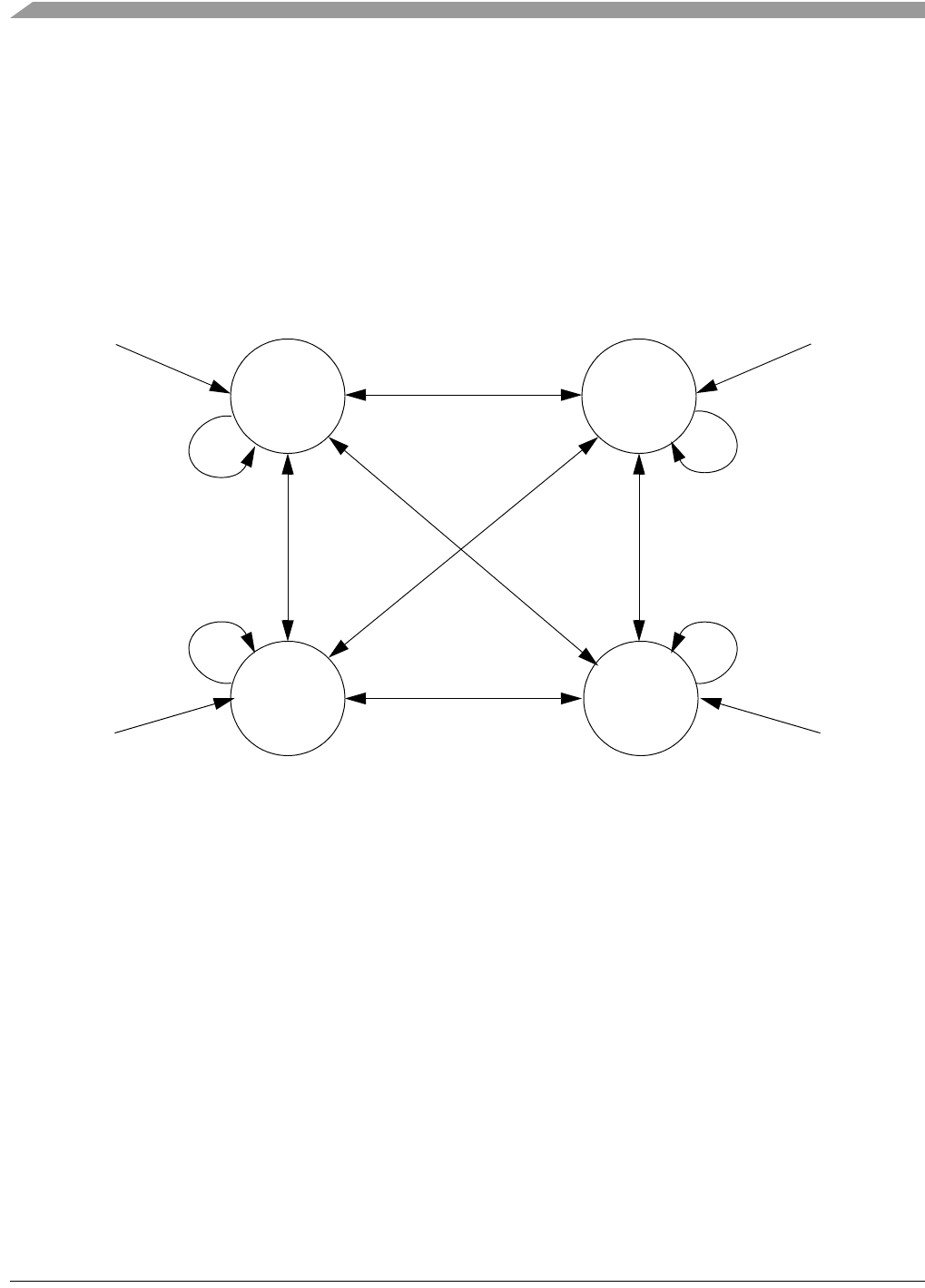
MCF548x Reference Manual, Rev. 3
16-8 Freescale Semiconductor
16.3 Functional Description
The system SRAM decodes the addresses for all four banks to determine which master is trying to access
which bank. The system SRAM module provides a bus arbitration mechanism for granting access of each
bank to each master. All masters simply request a data transfer and the SRAM grants a specified cycle
count to the appropriate master. The arbitration is overlapped with the address phase of SRAM transfers
and therefore imposes no performance penalty or overhead.
The current master pointer for each bank is determined as shown in Figure 16-7. The current master
pointer transitions to another master when the current master’s maximum transfer count is exceeded, or
the current master is idle and another master requests access to the bank. Otherwise, the current master
pointer remains unchanged.
Figure 16-7. SRAM Arbitration
Master
SEC
DMA-R
RESET
(Bank 0)
RESET
(Bank 1)
RESET
(Bank 2)
RESET
(Bank 3)
DMA-W

MCF548x Reference Manual, Rev. 3
Freescale Semiconductor 17-1
Chapter 17
FlexBus
17.1 Introduction
This chapter describes data transfer operations, error conditions, and reset operations. It describes transfers
initiated by the MCF548x and includes detailed timing diagrams showing the interaction of signals in
supported bus operations.
NOTE
Unless otherwise noted, in this chapter the term ‘clock’ refers to the CLKIN
used for the bus.
17.1.1 Overview
A multi-function external bus interface called the FlexBus interface controller is provided on the
MCF548x with basic functionality of interfacing to slave-only devices up to a maximum bus frequency of
66 MHz. It can be directly connected to asynchronous or synchronous devices such as external boot
ROMs, flash memories, gate-array logic, or other simple target (slave) devices with little or no additional
circuitry. For asynchronous devices a simple chip-select based interface can be used.
The FlexBus interface has six general purpose chip-selects (FBCS[5:0]). Chip-select FBCS0 can be
dedicated to boot ROM access and can be programmed to be byte (8 bits), word (16 bits), or longword (32
bits) wide. Control signal timing is compatible with common ROM / flash memories.
17.1.2 Features
The following list summarizes the key FlexBus features:
• Six independent, user-programmable chip-select signals (FBCS[5:0]) that can interface with
SRAM, PROM, EPROM, EEPROM, Flash, and other peripherals
• 8-, 16-, and 32-bit port sizes with configuration for multiplexed or non-multiplexed address and
data buses
• Byte, word, and longword, and line sized transfers
• Programmable burst and burst-inhibited transfers selectable for each chip select and transfer
direction
• Programmable address setup time with respect to the assertion of chip select
• Programmable address hold time with respect to the negation of chip select and transfer direction
17.1.3 Modes of Operation
The FlexBus interface is a configurable multiplexed bus that is set to one of four modes:
• Multiplexed 32-bit address and 32-bit data
• Multiplexed 32-bit address and 16-bit data (non-multiplexed 16-bit address and 16-bit data)
• Multiplexed 32-bit address and 8-bit data (non-multiplexed 24-bit address and 8-bit data)
• Non-multiplexed 32-bit address with 32-bit data
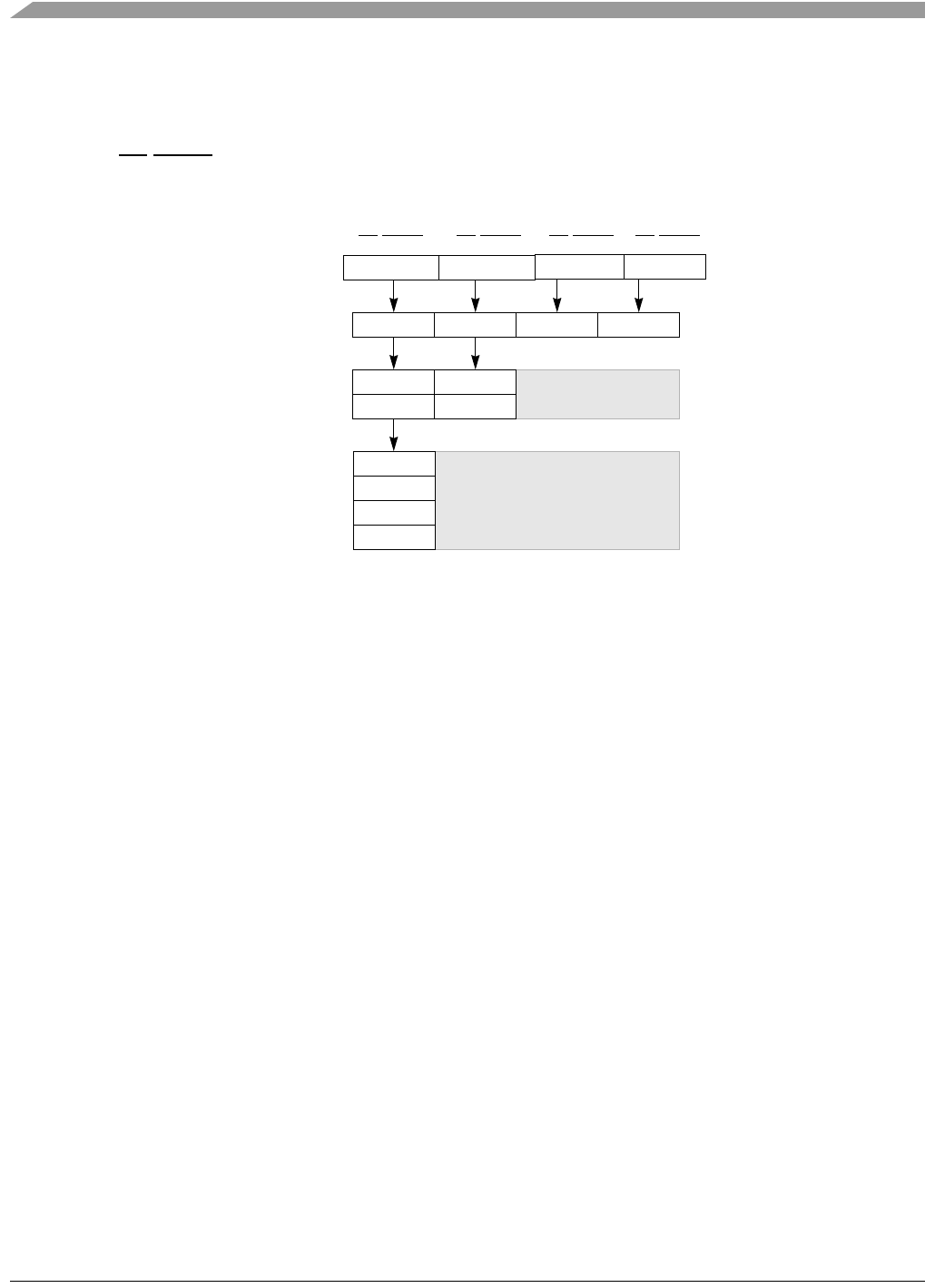
MCF548x Reference Manual, Rev. 3
17-2 Freescale Semiconductor
17.2 Byte Lanes
Figure 17-1 shows the byte lanes that external memory should be connected to and the sequential transfers
if a longword is transferred for three port sizes. For example, an 8-bit memory should be connected to
AD[31:24] (BE/BWE0). A longword transfer takes four transfers on AD[31:24], starting with the MSB
and going to the LSB.
Figure 17-1. Connections for External Memory Port Sizes
17.3 Address Latch
Because the FlexBus uses a multiplexed address and data bus, external logic might be needed in some
cases to capture the address phase as shown in Figure 17-2.
Processor
Data Bus
Byte 0
8-Bit Port
16-Bit Port
32-Bit Port
Byte 1
Byte 2
Byte 3
Byte 0 Byte 1
Byte 2 Byte 3
Byte 0 Byte 1 Byte 2 Byte 3
AD[31:24] AD[23:16] AD[15:8] AD[7:0]
External
Memory
Memory
Memory
Byte Select
Driven with
address values
Driven with
address values
BE/BWE0 BE/BWE1 BE/BWE2 BE/BWE3
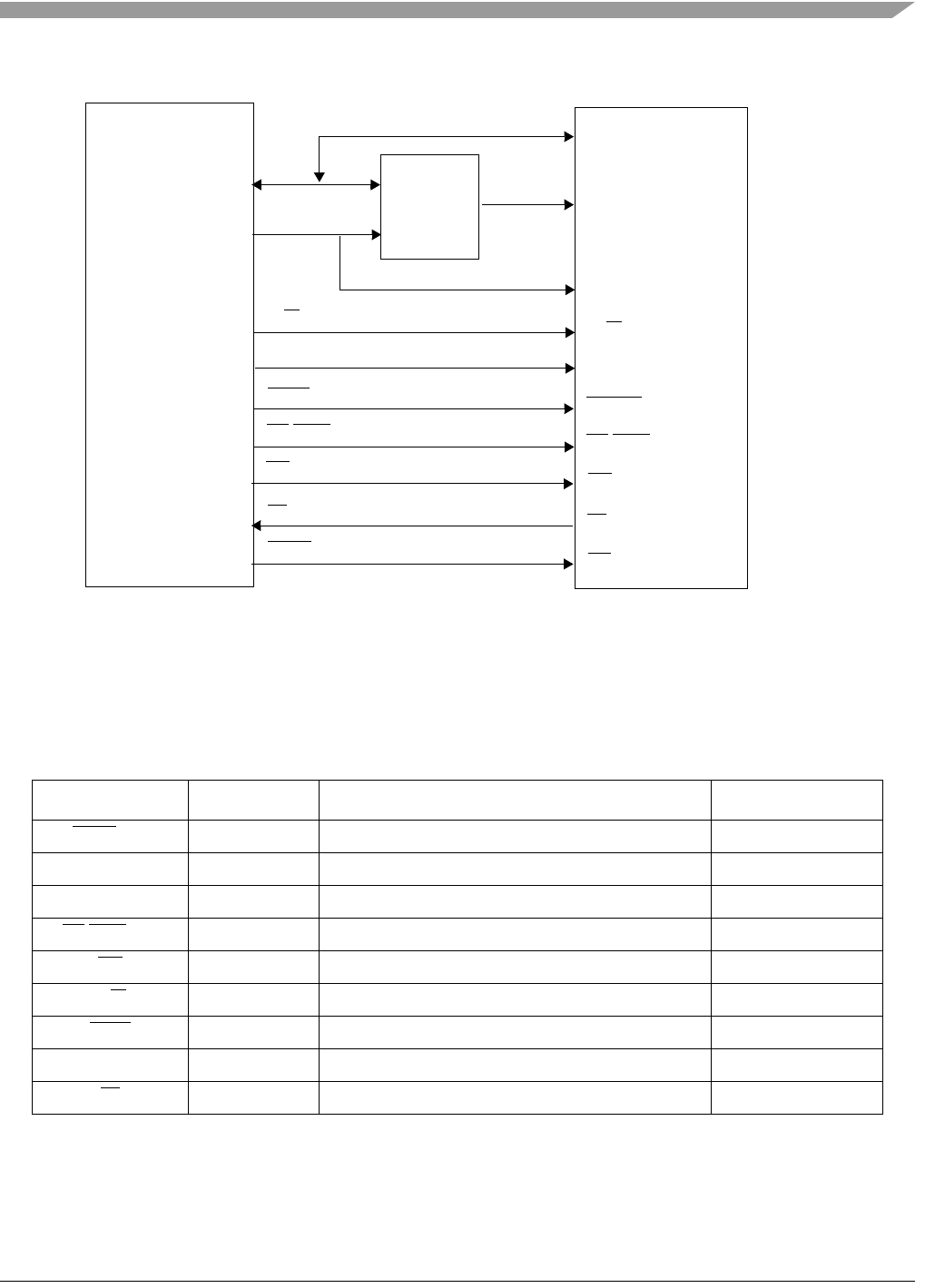
External Signals
MCF548x Reference Manual, Rev. 3
Freescale Semiconductor 17-3
Figure 17-2. Multiplexed FlexBus Implementation
17.4 External Signals
This section describes the external signals that are involved in data transfer operations. Table 17-1
summarizes the MCF548x FlexBus signals.
Table 17-1. FlexBus Signal Summary
Signal Name Direction Description Reset State
FBCS[5:0] O General purpose chip-selects Hi-Z
AD[31:0] I/O Address / Data bus Hi-Z
ALE O Address Latch Enable Hi-Z
BE/BWE[3:0] O Byte Selects Hi-Z
OE O Output Enable Hi-Z
R/W O Read/Write. 1 = Read, 0 = Write Hi-Z
TBST O Burst Transfer indicator Hi-Z
TSIZ[1:0] O Transfer Size Hi-Z
TA I Transfer Acknowledge —
AD[31:0]
FlexBus
Interface
Controller
DATA[31:Y]
ADDR[X:0]
Address
Latch
Logic
External Device / Peripheral
ALE
R/W
TA
FBCSx
ALE
R/W
TA
CS
BE/BWE[3:0]
BE/BWE[3:0]
OE OE
SIZ[1:0]
TSIZ[1:0]
TBST BURST

MCF548x Reference Manual, Rev. 3
17-4 Freescale Semiconductor
17.4.1 Chip-Select (FBCS[5:0])
The chip-select signal indicates which device is being selected. A particular chip-select asserts when the
transfer address is within the device’s address space as defined in the base and mask address registers, see
Section 17.5.2, “Chip-Select Registers.”
17.4.2 Address/Data Bus (AD[31:0])
The AD[31:0] bus carries address and data. The full 32-bit address is always driven on the first clock of a
bus cycle (address phase). The number of byte lanes used to carry the data during the data phase is
determined by the port size associated with the matching chip select.
In non-multiplexed mode, it is divided into sub-buses: address (output) and data (input/output). In
multiplexed mode, it carries the address during the address phase and the data during the data phase. Note
that in multiplexed mode and during the data phase, the address continues driving on the lower byte lanes
if these lanes are not used to carry the data.
17.4.3 Address Latch Enable (ALE)
The assertion of ALE indicates that the MCF548x has begun a bus transaction and that the address and
attributes are valid. ALE is asserted for one bus clock cycle. In multiplexed bus mode, ALE is used
externally as an address latch enable to capture the address phase of the bus transfer, as shown in
Figure 17-2.
17.4.4 Read/Write (R/W)
MCF548x drives the R/W signal to indicate the direction of the current bus operation. It is driven high
during read bus cycles and driven low during write bus cycles.
17.4.5 Transfer Burst (TBST)
Transfer Burst indicates that a burst transfer is in progress as driven by the MCF548x. A burst transfer can
be 2 to 16 beats depending on TSIZ[1:0] and the port size.
NOTE
When burst (TBST = 0) and transfer size is 16 bytes (TSIZ = 2’b11) and the
address is misaligned within the 16-byte boundary, the external device must
be able to wrap around the address.
17.4.6 Transfer Size (TSIZ[1:0])
For memory accesses, these signals, along with TBST, indicate the data transfer size of the current bus
operation. The FlexBus interface supports byte, word, and longword operand transfers and allows accesses
to 8-, 16-, and 32-bit data ports.
For misaligned transfers, TSIZ[1:0] indicate the size of each transfer. For example, if a longword access
through a 32-bit port device occurs at a misaligned offset of 0x1, a byte is transferred first
(TSIZ[1:0] = 01), a word is next transferred at offset 0x2 (TSIZ[1:0] = 10), then the final byte is
transferred at offset 0x4 (TSIZ[1:0] = 01).

External Signals
MCF548x Reference Manual, Rev. 3
Freescale Semiconductor 17-5
For aligned transfers larger than the port size, TSIZ[1:0] behaves as follows:
• If bursting is used, TSIZ[1:0] is driven to the size of transfer.
• If bursting is inhibited, TSIZ[1:0] first shows the size of the entire transfer and then shows the port
size.
For burst-inhibited transfers, TSIZ[1:0] changes with each ALE assertion to reflect the next transfer size.
For transfers to port sizes smaller than the transfer size, TSIZ[1:0] indicates the size of the entire transfer
on the first access and the size of the current port transfer on subsequent transfers. For example, for a
longword write to an 8-bit port, TSIZ[1:0] = 2’b00 for the first transaction and 2’b01 for the next three
transactions. If bursting is used and in the case of longword write to an 8-bit port, TSIZ[1:0] is driven to
2’b00 for the entire transfer.
17.4.7 Byte Selects (BE/BWE[3:0])
The byte strobe (BE/BWE[3:0]) outputs indicate that data is to be latched or driven onto a byte of the data
when driven low as shown in Table 17-1. BE/BWEn signals are asserted only to the memory bytes used
during a read or write access.
17.4.8 Output Enable (OE)
The output enable signal (OE) is sent to the interfacing memory and/or peripheral to enable a read transfer.
OE is asserted only when a chip select matches the current address decode.
17.4.9 Transfer Acknowledge (TA)
This signal indicates that the external data transfer is complete. During a read cycle, when the processor
recognizes TA, it latches the data and then terminates the bus cycle. During a write cycle, when the
processor recognizes TA, the bus cycle is terminated.
If auto-acknowledge is disabled, the external device drives TA to terminate the bus transfer; if
auto-acknowledge is enabled, the TA is generated internally after a specified wait states or the external
device may assert external TA before the wait-state countdown, terminating the cycle early. The MCF548x
negates FBCSn a cycle after the last TA asserts. During read cycles, the peripheral must continue to drive
data until TA is recognized. For write cycles, the processor continues to drive data one clock after FBCSn
is negated.
The number of wait states is determined either by internally programmed auto acknowledgement or by the
external TA input. If the external TA is used, the peripheral has total control on the number of wait states.
NOTE
External devices should only assert TA while the FBCSn signal to the
external device is asserted.
Table 17-2. Data Transfer Size
TSIZ[1:0] Transfer Size
00 4 bytes (longword)
01 1 byte
10 2 bytes (word)
11 16 bytes (line)

MCF548x Reference Manual, Rev. 3
17-6 Freescale Semiconductor
17.5 Chip-Select Operation
Each chip-select has a dedicated set of the following registers for configuration and control:
• Chip-select address registers (CSARn) control the base address space of the chip-select. See
Section 17.5.2.1, “Chip-Select Address Registers (CSAR0–CSAR5).”
• Chip-select mask registers (CSMRn) provide 16-bit address masking and access control. See
Section 17.5.2.2, “Chip-Select Mask Registers (CSMR0–CSMR5).”
• Chip-select control registers (CSCRn) provide port size and burst capability indication, wait-state
generation, address setup and hold times, and automatic acknowledge generation features. See
Section 17.5.2.3, “Chip-Select Control Registers (CSCR0–CSCR5).”
FBCS0 is a global chip-select after reset and provides re-locatable boot ROM capability.
17.5.1 General Chip-Select Operation
When a bus cycle is initiated, the MCF548x first compares its address with the base address and mask
configurations programmed for chip-selects 0–5 (configured in CSCR0–CSCR5). If the driven address
matches a programmed chip-select, the appropriate chip-select is asserted fulfilling the requirements as
programmed in the respective configuration register.
17.5.1.1 8-, 16-, and 32-Bit Port Sizing
Static bus sizing is programmable through the port size bits, CSCR[PS]. See Section 17.5.2.3,
“Chip-Select Control Registers (CSCR0–CSCR5).” Note that the MCF548x always drives 32-bit address
on the AD bus in the first cycle regardless of the external device’s address size. The external device must
connect its address lines to the appropriate AD bits starting from AD0 and upward. It must also connect
its data lines to the AD bus starting from the AD31 and downward. No bit ordering is required when
connecting address and data lines to the AD bus. For example, a 16-bit address/16-bit data device would
connect its addr[15:0] to AD[15:0] and data[15:0] to AD[31:16]. See Figure 17-6 for graphical connection.
17.5.1.2 Global Chip-Select Operation
FBCS0, the global (boot) chip-select, allows address decoding for boot ROM before system initialization.
Its operation differs from other external chip-select outputs after system reset.
After system reset, FBCS0 is asserted for every external access. No other chip-select can be used until the
valid bit, CSMR0[V], is set, at which point FBCS0 functions as configured. After this, FBCS[5:1] can be
used as well. At reset, the port size, and automatic acknowledge functions of the global chip-select are
determined by the logic levels on the AD[2:0] signals. Table 17-3, Table 17-4, and Table 17-5 list the
various reset encodings for the configuration signals.
Table 17-3. AD4/FB_CONFIG Selection of Non-Multiplexed
32-bit Address/32-bit Data Mode
AD4 FlexBus Operating Mode
0 AD[31:0] used for data.
PCIAD[31:0] used for address1
1If the non-multiplexed 32-bit address/32-bit data mode is selected the PCI bus
cannot be used.
1 PCIAD[31:0] used for PCI bus.
AD[31:0] used for both address and data.

Chip-Select Operation
MCF548x Reference Manual, Rev. 3
Freescale Semiconductor 17-7
17.5.2 Chip-Select Registers
The following tables describe in detail the registers and bit meanings for configuring chip-select operation.
The chip-select controller register map is accessed relative to the memory base address register (MBAR).
Table 17-6 shows the chip-select register memory map. Reading unused or reserved locations terminates
normally and returns zeros.
Table 17-4. AD[2]/AA Automatic Acknowledge of Boot FBCS0
AD[2]/AA Boot FBCS0 AA Configuration at Reset
0 Disabled
1 Enabled with 63 wait states
Table 17-5. AD[1:0]/PS[1:0], Port Size of Boot FBCS0
AD[1:0]/PS[1:0] Boot FBCS0 Port Size at Reset
00 32-bit port
01 8-bit port
1x 16-bit port
Table 17-6. Chip-Select Registers
Register
Offset [31:24] [23:16] [15:8] [7:0] ResetValue Access 1
0x0500 Chip-select address register—bank 0 (CSAR0) 0x0000_0000 R/W
0x0504 Chip-select mask register—bank 0 (CSMR0) 0x0000_0000 R/W
0x0508 Chip-select control register—bank 0 (CSCR0) BSTW = 0
BSTR = 0
PS = AD[1:0]
AA = AD[2]
WS = 111111
WRAH = 11
RDAH = 11
ASET = 11
SWSEN = 0
SWS = 000000
R/W
0x050C Chip-select address register—bank 1 (CSAR1) 0x0000_0000 R/W
0x0510 Chip-select mask register—bank 1 (CSMR1) 0x0000_0000 R/W
0x054 Chip-select control register—bank 1 (CSCR1) 0x0000_0000 R/W
0x0518 Chip-select address register—bank 2 (CSAR2) 0x0000_0000 R/W
0x051C Chip-select mask register—bank 2 (CSMR2) 0x0000_0000 R/W
0x0520 Chip-select control register—bank 2 (CSCR2) 0x0000_0000 R/W
0x0524 Chip-select address register—bank 3 (CSAR3) 0x0000_0000 R/W
0x0528 Chip-select mask register—bank 3 (CSMR3) 0x0000_0000 R/W

MCF548x Reference Manual, Rev. 3
17-8 Freescale Semiconductor
1 The access column indicates whether the corresponding register allows both read/write functionality (R/W), read-only
functionality (R), or write-only functionality (W). A read access to a write-only register returns zeros. A write access to a
read-only register has no effect.
2 Addresses not assigned to a register and undefined register bits are reserved for expansion. Write accesses to these reserved
address spaces and reserved register bits have no effect.
17.5.2.1 Chip-Select Address Registers (CSAR0–CSAR5)
CSARn, Figure 17-3, specify the chip-select base addresses.
0x052C Chip-select control register—bank 3 (CSCR3) 0x0000_0000 R/W
0x0530 Chip-select address register—bank 4 (CSAR4) 0x0000_0000 R/W
0x0534 Chip-select mask register—bank 4 (CSMR4) 0x0000_0000 R/W
0x0538 Chip-select control register—bank 4 (CSCR4) 0x0000_0000 R/W
0x053C Chip-select address register—bank 5 (CSAR5) 0x0000_0000 R/W
0x0540 Chip-select mask register—bank 5 (CSMR5) 0x0000_0000 R/W
0x0544 Chip-select control register—bank 5 (CSCR5) 0x0000_0000 R/W
31 30 29 28 27 26 25 24 23 22 21 20 19 18 17 16
RBA
W
Reset0000000000000000
1514131211109876543210
R0000000000000000
W
Reset0000000000000000
Reg
Addr
MBAR + 0x500 (CSAR0); 0x50C (CSAR1); 0x518 (CSAR2);
0x524 (CSAR3); 0x530 (CSAR4); 0x53C (CSAR5)
Figure 17-3. Chip-Select Address Registers (CSARn)
Table 17-7. CSARn Field Descriptions
Bits Name Description
31–16 BA Base address. Defines the base address for memory dedicated to chip-select FBCSn. BA is
compared to bits 31–16 on the internal address bus to determine if chip-select memory is being
accessed.
15–0 — Reserved, should be cleared
Table 17-6. Chip-Select Registers (Continued)
Register
Offset [31:24] [23:16] [15:8] [7:0] ResetValue Access 1

Chip-Select Operation
MCF548x Reference Manual, Rev. 3
Freescale Semiconductor 17-9
17.5.2.2 Chip-Select Mask Registers (CSMR0–CSMR5)
CSMRn, Figure 17-4, are used to specify the address mask and allowable access types for the respective
chip-selects.
Table 17-8 describes CSMR fields.
31 30 29 28 27 26 25 24 23 22 21 20 19 18 17 16
R BAM
W
Reset0000000000000000
1514131211109876543210
R0000000WP0000000V
W
Reset0000000000000000
Reg
Addr
MBAR + 0x504 (CSMR0); 0x510 (CSMR1); 0x51C (CSMR2);
0x528 (CSMR3); 0x534 (CSMR4); 0xr540 (CSMR5)
Figure 17-4. Chip-Select Mask Registers (CSMRn)
Table 17-8. CSMRn Field Descriptions
Bits Name Description
31–16 BAM Base address mask. Defines the chip-select block size by masking address bits. Setting a BAM bit
causes the corresponding CSAR bit to be a “don’t care” in the decode.
0 Corresponding address bit is used in chip-select decode.
1 Corresponding address bit is a don’t care in chip-select decode.
The block size for FBCSn is 2n; n = (number of bits set in respective CSMR[BAM]) + 16.
For example, if CSAR0 = 0x0000 and CSMR0[BAM] = 0x0008, FBCS0 would address two
discontinuous 64-Kbyte memory blocks: one from 0x0000–0xFFFF and one from
0x8_0000–0x8_FFFF.
Likewise, for FBCS0 to access 32 Mbytes of address space starting at location 0x0, FBCS1 must
begin at the next byte after FBCS0 for a 16-Mbyte address space. Then CSAR0 = 0x0000,
CSMR0[BAM] = 0x01FF, CSAR1 = 0x0200, and CSMR1[BAM] = 0x00FF.
15–9 — Reserved, should be cleared
8 WP Write protect. Controls write accesses to the address range in the corresponding CSAR. Attempting
to write to the range of addresses for which CSARn[WP] = 1 results in the appropriate chip-select not
being selected. No exception occurs.
0 Both read and write accesses are allowed
1 Only read accesses are allowed
7–1 — Reserved, should be cleared
0 V Valid bit. Indicates whether the corresponding CSAR, CSMR, and CSCR contents are valid.
Programmed chip-selects do not assert until V bit is set (except for FBCS0, which acts as the global
chip-select). Reset clears each CSMRn[V]. At reset, no chip-select other than FBCS0 can be used
until the CSMR0[V] is set. At which point FBCS[5:0] functions as configured.
0 chip-select invalid
1 chip-select valid

MCF548x Reference Manual, Rev. 3
17-10 Freescale Semiconductor
17.5.2.3 Chip-Select Control Registers (CSCR0–CSCR5)
Each CSCRn, Figure 17-5, controls the auto acknowledge, address setup and hold times, port size, burst
capability, and activation of each chip-select. Note that to support the global chip-select, FBCS0, the
CSCR0 reset values differ from the other CSCRs. FBCS0 allows address decoding for boot ROM before
system initialization.
Table 17-9 describes CSCRn fields.
31 30 29 28 27 26 25 24 23 22 21 20 19 18 17 16
RSWS 00SWS
EN
— ASET RDAH WRAH
W
Reset: CSCR0000000000011 1 111
Reset: CSCRs000000000000 0 000
151413121110987654 3 210
RWS 0AA PS BEM BSTR BSTW000
W
Reset: CSCR01111110AD2AD[1:0]AD30 0 000
Reset: CSCRs000000000000 0 000
Reg
Addr
MBAR + 0x508 (CSCR0); 0x514 (CSCR1); 0x520 (CSCR2);
0x52C (CSCR3); 0x538 (CSCR4); 0x544 (CSCR5)
Figure 17-5. Chip-Select Control Registers (CSCRn)
Table 17-9. CSCRn Field Descriptions
Bits Name Description
31–26 SWS Secondary wait states. The number of wait states inserted before an internal transfer acknowledge
is generated for burst transfer except for the first termination, which is controlled by the wait state
count. The secondary wait state is only used if the secondary wait state enable is set, otherwise the
wait state value is used for all burst transfers.
25–24 — Reserved, should be cleared
23 SWSEN Secondary wait state enable. If set (SWSEN = 1), then the secondary wait state value is used to
insert wait states before an internal transfer acknowledge is generated for burst transfer secondary
terminations. If cleared (SWSEN = 0), then the wait state value is used to insert wait states before
an internal transfer acknowledge is generated for all transfers.
22 — Reserved, should be cleared
21–20 ASET Address setup. This field controls the asserting of chip-select with respect to assertion of a valid
address and attributes. Note that the address and attributes are considered valid at the same time
ALE asserts.
00 Assert chip-select on rising clock edge after address is asserted. (Default FBCSn)
01 Assert chip-select on second rising clock edge after address is asserted.
10 Assert chip-select on third rising clock edge after address is asserted.
11 Assert chip-select on fourth rising clock edge after address is asserted.(Reset FBCS0)

Chip-Select Operation
MCF548x Reference Manual, Rev. 3
Freescale Semiconductor 17-11
19–18 RDAH Read Address Hold or (Deselect). This field controls the address and attribute hold time after the
termination during a read cycle that hits in the chip-select address space. The hold time only applies
at the end of a transfer. Therefore, a burst transfer only has a hold time added after the last bus
cycle.
RDAH = 00; Hold address and attributes one cycle after FBCSn negates on reads. (Default FBCSn)
01 Hold address and attributes two cycles after FBCSn negates on reads.
10 Hold address and attributes three cycles after FBCSn negates on reads.
11 Hold address and attributes four cycles after FBCSn negates on reads. (Reset FBCS0)
17–16 WRAH Write Address Hold or (Deselect). This field controls the address, data and attribute hold time after
the termination of a write cycle that hits in the chip-select address space.The hold time only applies
at the end of a transfer. Therefore, a burst transfer only has a hold time added after the last bus
cycle.
WRAH = 00; Hold address and attributes one cycle after FBCSn negates on writes. (Default
FBCSn)
01 Hold address and attributes two cycles after FBCSn negates on writes.
10 Hold address and attributes three cycles after FBCSn negates on writes.
11 Hold address and attributes four cycles after FBCSn negates on writes. (Reset FBCS0)
15–10 WS Wait states. The number of wait states inserted after FBCSn asserts and before an internal transfer
acknowledge is generated (WS = 0 inserts zero wait states, WS = 0x3F inserts 63 wait states). If
AA = 0, TA must be asserted by the external system regardless of the number of wait states
generated. In that case, the external transfer acknowledge ends the cycle. An external TA
supersedes the generation of an internal TA.
9 — Reserved, should be cleared.
8 AA Auto-acknowledge enable. Determines the assertion of the internal transfer acknowledge for
accesses specified by the chip-select address.
0 No internal TA is asserted. Cycle is terminated externally.
1 Internal TA is asserted as specified by WS. Note that if AA = 1 for a corresponding FBCSn and
the external system asserts an external TA before the wait-state countdown asserts the internal TA,
the cycle is terminated. Burst cycles increment the address bus between each internal termination.
7–6 PS Port size. Specifies the width of the data port associated with each chip-select. It determines where
data is driven during write cycles and where data is sampled during read cycles.
00 32-bit port size. Valid data sampled and driven on D[31:0]
01 8-bit port size. Valid data sampled and driven on D[31:24]
1x 16-bit port size. Valid data sampled and driven on D[31:16]
5 BEM Byte enable mode. Specifies the byte enable operation. Certain SRAMs have byte enables that
must be asserted during reads as well as writes. BEM can be set in the relevant CSCR to provide
the appropriate mode of byte enable support in support of these SRAMs.
0 Neither BE or BWE is asserted for reads. BWE is generated for data write only.
1BE
is asserted for reads; BWE is asserted for writes.
4 BSTR Burst read enable. Specifies whether burst reads are used for memory associated with each
FBCSn.
0 Data exceeding the specified port size is broken into individual, port-sized non-burst reads. For
example, a longword read from an 8-bit port is broken into four 8-bit reads.
1 Enables data burst reads larger than the specified port size, including longword reads from 8-
and 16-bit ports and word reads from 8-bit ports.
Table 17-9. CSCRn Field Descriptions (Continued)
Bits Name Description

MCF548x Reference Manual, Rev. 3
17-12 Freescale Semiconductor
17.6 Functional Description
17.6.1 Data Transfer Operation
Data transfers between the MCF548x and other devices involve the following signals:
• Address/data bus (AD[31:0])
• Control signals (ALE and TA)
•FBCSn
•OE
•BE/BWE[3:0]
• Attribute signals (R/W, TBST, TSIZ[1:0])
The address and write data (AD[31:0]), R/W, ALE, FBCSn, and all attribute signals change on the rising
edge of the clock. Read data is registered in the MCF548x on the rising edge of the clock.
The MCF548x FlexBus supports byte, word, and longword operand transfers and allows accesses to 8-,
16-, and 32-bit data ports.Transfer parameters such as address setup and hold, port size, the number of wait
states for the external device being accessed, automatic internal transfer termination enable or disable, and
burst enable or disable are programmed in the chip-select control registers (CSCRs), Section 17.5.2.3,
“Chip-Select Control Registers (CSCR0–CSCR5).”
17.6.2 Data Byte Alignment and Physical Connections
The MCF548x aligns data transfers in FlexBus byte lanes, the number of lanes depending on the width of
the data port. Figure 17-6 shows the byte lanes that external memory should be connected to and the
sequential transfers if a longword is transferred for three port sizes. For example, an 8-bit memory should
be connected to the single lane AD[31:24]. A longword transfer through this 8-bit port takes four transfers
on AD[31:24], starting with the MSB and going to the LSB. A longword transfer through a 32-bit port
requires one transfer on each of the four byte lanes of the FlexBus.
3 BSTW Burst write enable. Specifies whether burst writes are used for memory associated with each
FBCSn.
0 Break data larger than the specified port size into individual port-sized, non-burst writes. For
example, a longword write to an 8-bit port takes four byte writes.
1 Enables burst write of data larger than the specified port size, including longword writes to 8 and
16-bit ports and word writes to 8-bit ports.
2–0 — Reserved, should be cleared.
Table 17-9. CSCRn Field Descriptions (Continued)
Bits Name Description
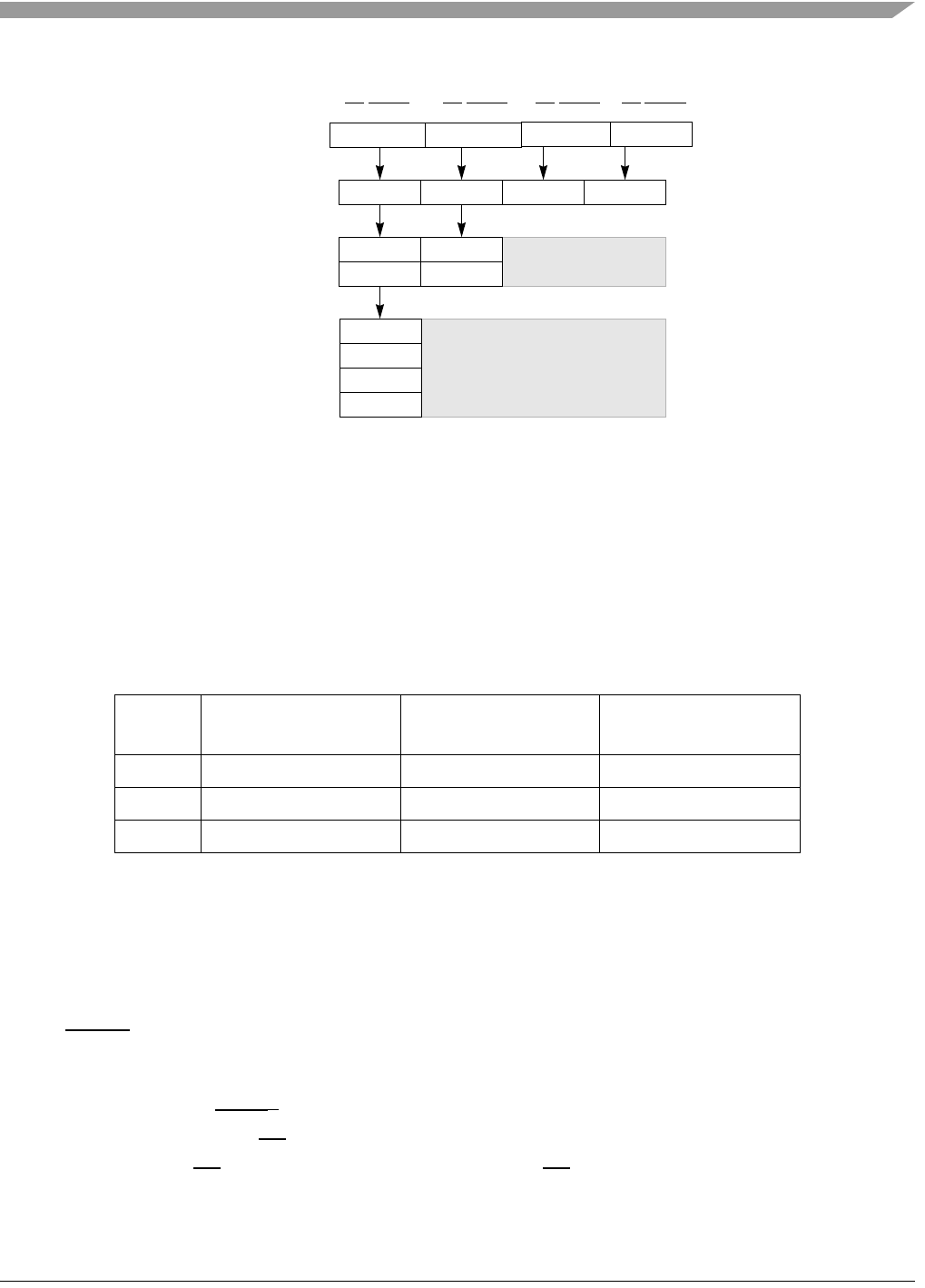
Functional Description
MCF548x Reference Manual, Rev. 3
Freescale Semiconductor 17-13
Figure 17-6. Connections for External Memory Port Sizes
17.6.3 Address/Data Bus Multiplexing
The MCF548x FlexBus uses a 32-bit wide multiplexed address and data bus (AD[31:0]). The full 32-bit
address will always be driven on the first clock of a bus cycle. During the data phase, which AD[31:0] lines
are used for data is determined by the programmed port size for the corresponding chip select. The
MCF548x continues to drive the address on any AD[31:0] lines that are not used for data.
Table 17-10 lists the supported combinations of address and data bus widths.
17.6.4 Bus Cycle Execution
As shown in Figure 17-9 and Figure 17-11, basic bus operations occur in four clocks, as follows:
1. At the first clock edge, the address, attributes, and ALE are driven.
2. FBCSn is asserted at the second rising clock edge to indicate which device has been selected and
by that time the address and attributes are valid and stable. ALE is negated at this edge.
For a write transfer, data is driven on the bus at this clock edge and continues to be driven until one
clock cycle after FBCSn negates. For a read transfer, data is also returned at this cycle.
External slave asserts TA at this clock edge.
3. Read data and TA are sampled on the third clock edge. TA can be negated after this edge and read
data can then be tristated.
Table 17-10. FlexBus Operating Modes
Port Size Address Signals During
Address Phase
Data Signals During
Data Phase
Address Signals During
Data Phase
32-bit1AD[31:0] AD[31:0] --
16-bit AD[31:0] AD[31:16] AD[15:0]
8-bit AD[31:0] AD[31:24] AD[23:0]
1The 32-bit Address/32-bit Data non-multiplexed mode uses the PCI address/data bus to
provide a second 32-bit bus for the address. PCI cannot be used if this mode is selected.
Processor
Data Bus
Byte 0
8-Bit Port
16-Bit Port
32-Bit Port
Byte 1
Byte 2
Byte 3
Byte 0 Byte 1
Byte 2 Byte 3
Byte 0 Byte 1 Byte 2 Byte 3
AD[31:24] AD[23:16] AD[15:8] AD[7:0]
External
Memory
Memory
Memory
Byte Select
Driven with
address values
Driven with
address values
BE/BWE0 BE/BWE1 BE/BWE2 BE/BWE3
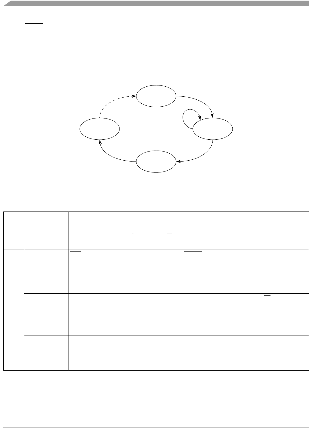
MCF548x Reference Manual, Rev. 3
17-14 Freescale Semiconductor
4. FBCSn is negated at the fourth rising clock edge. This last clock of the bus cycle uses what would
be an idle clock between cycles to provide hold time for address, attributes, and write data.
17.6.4.1 Data Transfer Cycle States
The data transfer operation in the MCF548x is controlled by an on-chip state machine. The state transition
diagram for basic read and write cycles is shown in Figure 17-7.
Figure 17-7. Data Transfer State Transition Diagram
Table 17-11 describes the states as they appear in subsequent timing diagrams.
Table 17-11. Bus Cycle States
State Cycle Description
S0 All The read or write cycle is initiated. On the rising clock edge, the MCF548x places a valid address
on AD[31:0], asserts ALE, and drives R/W high for a read and low for a write, if these signals are
not already in the appropriate state.
S1 All ALE is negated on the rising edge of CLK, and FBCSn is asserted. Data is driven on AD[31:Y] for
writes, and AD[31:Y] is three-stated for reads. Address continues to be driven on AD[X:0] pins that
are unused for data.
If TA is recognized asserted, then the cycle moves on to S2. If TA is not asserted either internally
or externally, then the S1 state continues to repeat.
Read Data is made available by the external device before the rising edge of CLK with TA asserted. The
the MCF548x will latch data on this rising clock edge.
S2 All For internal termination, both the FBCSn and internal TA will be negated. For external termination,
the external device should negate TA, and FBCSn select is negated after the rising edge of CLK at
the end of S2.
Read The external device can stop driving data after the rising edge of CLK at the beginning of S2.
However, data can be driven until the end of S3 or any additional address hold cycles.
S3 All Address, data, and R/W go invalid off the rising edge of CLK at the end of S3, terminating the read
or write cycle.
S0
S1
S2
Wait States
S3
Next Cycle
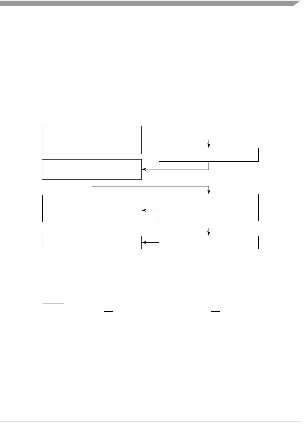
Functional Description
MCF548x Reference Manual, Rev. 3
Freescale Semiconductor 17-15
17.6.5 FlexBus Timing Examples
17.6.5.1 Basic Read Bus Cycle
During a read cycle, the MCF548x receives data from memory or from a peripheral device. Figure 17-8 is
a read cycle flowchart.
NOTE
Throughout this chapter AD[X:0] is used to indicate an address bus that can
be 32-, 24-, or 16-bits in width. AD[31:Y] is a data bus that can be 32-, 16-,
or 8-bits wide.
Figure 17-8. Read Cycle Flowchart
The read cycle timing diagram is shown in Figure 17-9.
NOTE
In the following timing diagrams, the dotted lines indicate TA, OE, and
FBCSn timing when internal termination is used (CSCR[AA] = 1). The
external and internal TA assert at the same time; however, TA is not driven
externally for internally terminated bus cycles.
1. Select the appropriate slave device.
Drive data on AD[31:Y].
Assert TA (external termination).
2.
3.
1. Negate TA (external termination).
1. Decode address.
1. Set R/W to read.
Place address on AD[31:0].
Assert ALE.
2.
3.
1. Negate ALE.
Assert FBCSn.2.
1. CS unit asserts internal TA (auto
acknowledge/internal termination).
Sample TA low and latch data.2.
1. Start next cycle.
MCF548X System
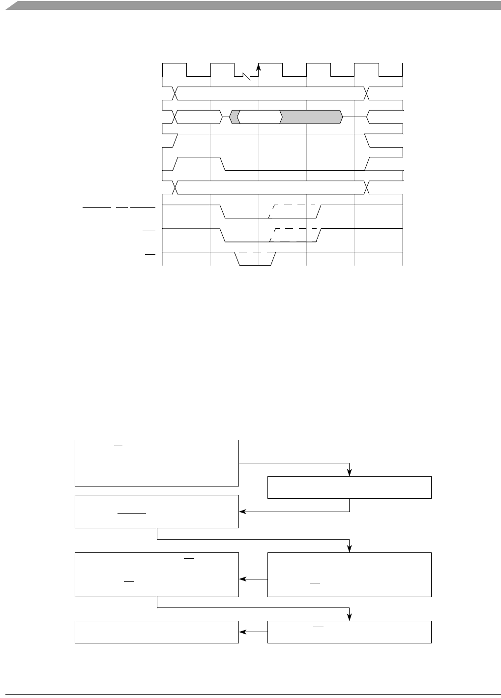
MCF548x Reference Manual, Rev. 3
17-16 Freescale Semiconductor
Figure 17-9. Basic Read Bus Cycle
17.6.5.2 Basic Write Bus Cycle
During a write cycle, the MCF548x sends data to memory or to a peripheral device. The write cycle
flowchart is shown in Figure 17-10.
NOTE
Throughout this chapter AD[X:0] is used to indicate an address bus that can
be 32-, 24-, or 16-bits in width. AD[31:Y] is a data bus that can be 32-, 16-,
or 8-bits wide.
Figure 17-10. Write Cycle Flowchart
CLK
AD[X:0]
AD[31:Y]
R/W
ALE
FBCSn, BE/BWEn
TA
OE
S0 S1 S2 S3
ADDR[X:0]
A[31:Y]DATA
TSIZ[1:0] TSIZ[1:0]
1. Select the appropriate slave device.
Drive data on AD[31:Y].
Assert TA (external termination).
2.
3.
1. Negate TA (external termination).
1. Decode address.
1. Set R/W to write.
Place address on AD[31:0].
Assert ALE.
2.
3.
1. Negate ALE.
Assert FBCSn.2.
1. CS unit asserts internal TA (auto
acknowledge/internal termination).
Sample TA low.2.
1. Start next cycle.
MCF548X System
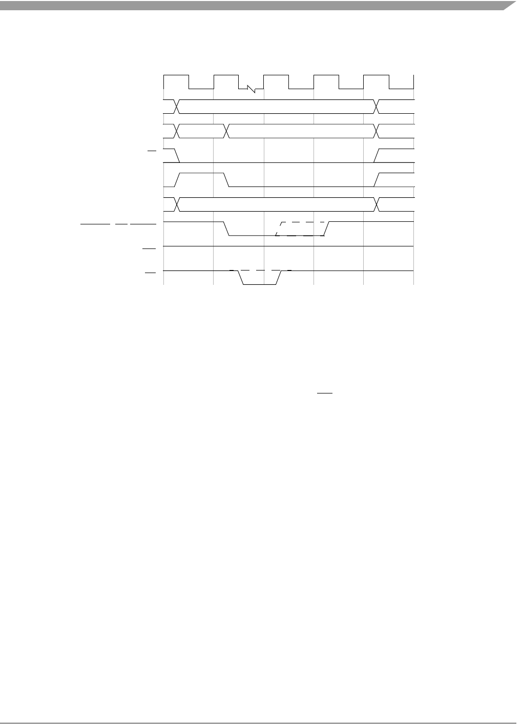
Functional Description
MCF548x Reference Manual, Rev. 3
Freescale Semiconductor 17-17
The write cycle timing diagram is shown in Figure 17-11.
Figure 17-11. Basic Write Bus Cycle
17.6.5.3 Bus Cycle Multiplexing
This section shows timing diagrams for various port size scenarios. Figure 17-12 illustrates the basic word
read transfer to a 16-bit device with no wait states. The address is driven on the full AD[31:0] bus in the
first clock. The MCF548x tristates AD[31:16] on the second clock and continues to drive address on
AD[15:0] throughout the bus cycle. The external device returns the read data on AD[31:16] and may
tristate the data line or continue to drive the data one clock after TA is sampled asserted.
CLK
AD[X:0]
AD[31:Y]
R/W
ALE
FBCSn, BE/BWEn
TA
OE
S0 S1 S2 S3
ADDR[X:0]
A[31:Y]DATA
TSIZ[1:0] TSIZ[1:0]
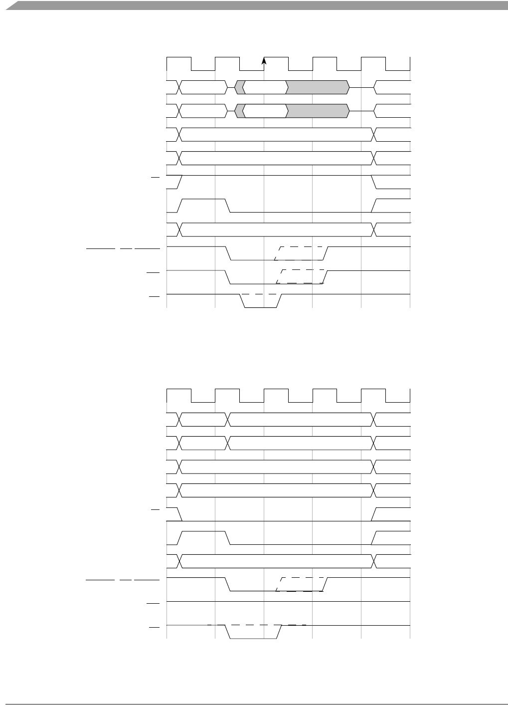
MCF548x Reference Manual, Rev. 3
17-18 Freescale Semiconductor
Figure 17-12. Single Word Read Transfer with Muxed 32-A / 16-D
or Non-Muxed 16-A / 16-D
Figure 17-13 shows the similar configuration for a write transfer. The data is driven from the second clock
on AD[31:16].
Figure 17-13. Single Word Write Transfer with Muxed 32-A / 16-D
or Non-Muxed 16-A / 16-D
CLK
S0 S1 S2 S3
AD[31:24]
R/W
ALE
FBCSn, BE/BWEn
TA
OE
AD[15:8]
AD[7:0]
AD[23:16]
A[31:24] D[15:8]
ADDR[15:8]
A[23:16] D[7:0]
ADDR[7:0]
TSIZ[1:0] 10
CLK
S0 S1 S2 S3
AD[31:24]
R/W
ALE
TA
OE
FBCSn, BE/BWEn
A[31:24] DATA[15:8]
AD[15:8]
AD[7:0]
AD[23:16] A[23:16] DATA[7:0]
ADDR[15:8]
ADDR[7:0]
TSIZ[1:0] 10
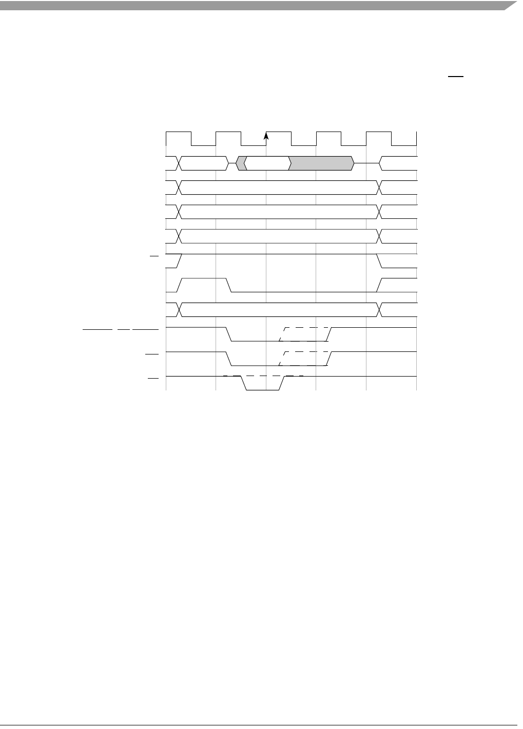
Functional Description
MCF548x Reference Manual, Rev. 3
Freescale Semiconductor 17-19
Figure 17-14 illustrates the basic byte read transfer to an 8-bit device with no wait states. The address is
driven on the full AD[31:0] bus in the first clock. The MCF548x tristates AD[31:24] on the second clock
and continues to drive address on AD[23:0] throughout the bus cycle. The external device returns the read
data on AD[31:24], and may tristate the data line or continue to drive the data one clock after TA is sampled
asserted.
Figure 17-14. Single Byte Read Transfer with Muxed 32-A / 8-D
or Non-Muxed 24-A / 8-D
Figure 17-15 shows the similar configuration for a write transfer. The data is driven from the second clock
on AD[31:24].
CLK
S0 S1 S2 S3
AD[31:24]
R/W
ALE
TA
OE
FBCSn, BE/BWEn
AD[15:8]
AD[7:0]
AD[23:16] ADDR[23:16]
A[31:24] D[7:0]
ADDR[15:8]
ADDR[7:0]
TSIZ[1:0] 01
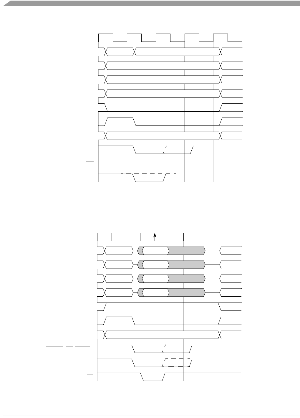
MCF548x Reference Manual, Rev. 3
17-20 Freescale Semiconductor
Figure 17-15. Single Byte Write Transfer with Muxed 32-A / 8-D
or Non-Muxed 24-A / 8-D
Figure 17-16 depicts a longword read through a 32-bit device. Notice that when the device port size is 32
bits, the only mode the bus supports is multiplexing address and data lines.
Figure 17-16. Longword Read Transfer with Muxed 32-A / 32-D
CLK
S0 S1 S2 S3
AD[31:24]
R/W
ALE
TA
OE
FBCSn, BE/BWEn
A[31:24] DATA[7:0]
AD[15:8]
AD[7:0]
AD[23:16] ADDR[23:16]
ADDR[15:8]
ADDR[7:0]
TSIZ[1:0] 01
CLK
S0 S1 S2 S3
AD[31:24]
R/W
ALE
TA
OE
FBCSn, BE/BWEn
AD[15:8]
AD[7:0]
AD[23:16] A[23:16] D[23:16]
A[31:24] D[31:24]
A[15:8] D[15:8]
A[7:0] D[7:0]
TSIZ[1:0] 00
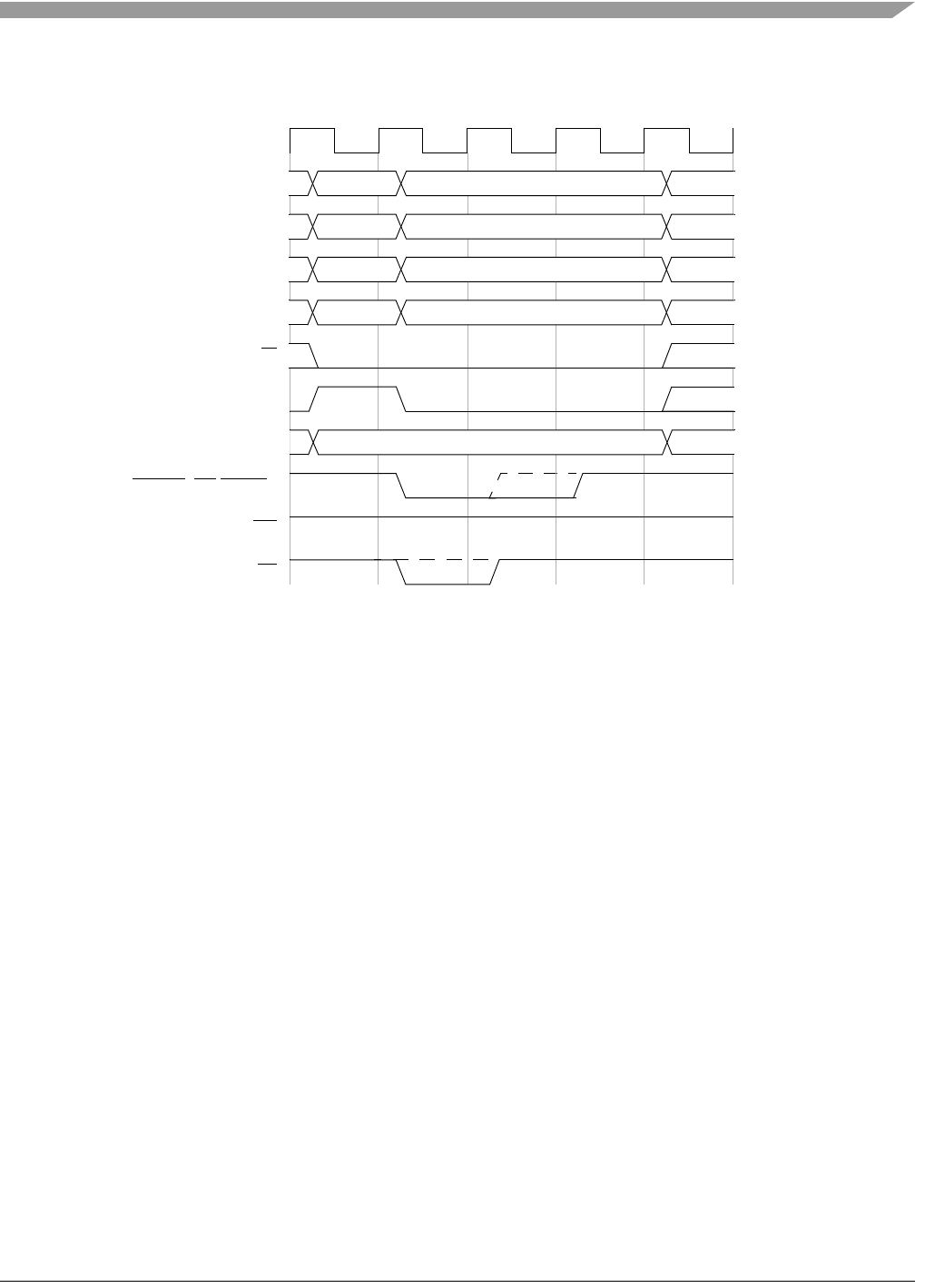
Functional Description
MCF548x Reference Manual, Rev. 3
Freescale Semiconductor 17-21
Figure 17-17 illustrates the longword write to a 32-bit device.
Figure 17-17. Longword Write Transfer with Muxed 32-A / 32-D
17.6.5.4 Timing Variations
The MCF548x has several features that can be used to change the timing characteristics of a basic read or
write bus cycle to provide additional address setup, address hold, and time for a device to provide or latch
data.
17.6.5.4.1 Wait States
Wait states can be inserted before each beat of a transfer by programming the CSCRn registers. Wait states
can be used to give the peripheral or memory more time to return read data or sample write data.
Figure 17-18 and Figure 17-19 show the basic read and write bus cycles (also shown in Figure 17-9 and
Figure 17-11). This is the default case with no wait states.
CLK
S0 S1 S2 S3
AD[31:24]
R/W
ALE
TA
OE
FBCSn, BE/BWEn
A[31:24] DATA[31:24]
AD[15:8] A[15:8] DATA[15:8]
AD[7:0] A[7:0] DATA[7:0]
AD[23:16] A[23:16] DATA[23:16]
TSIZ[1:0] 00
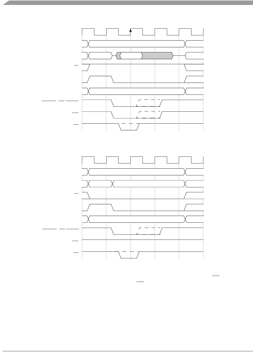
MCF548x Reference Manual, Rev. 3
17-22 Freescale Semiconductor
Figure 17-18. Basic Read Bus Cycle (No Wait States)
Figure 17-19. Basic Write Bus Cycle (No Wait States)
If wait states are used, then the S1 state will repeat continuously until either the internal TA is asserted by
the chip select auto-acknowledge unit or the external TA is recognized as asserted. Figure 17-20 and
Figure 17-21 show a read and write cycle with one wait state.
CLK
AD[X:0]
AD[31:Y]
R/W
ALE
TA
OE
S0 S1 S2 S3
FBCSn, BE/BWEn
ADDR[X:0]
A[31:Y]DATA
TSIZ[1:0] TSIZ[1:0]
CLK
AD[X:0]
AD[31:Y]
R/W
ALE
TA
OE
S0 S1 S2 S3
FBCSn, BE/BWEn
ADDR[X:0]
A[31:Y]DATA
TSIZ[1:0] TSIZ[1:0]
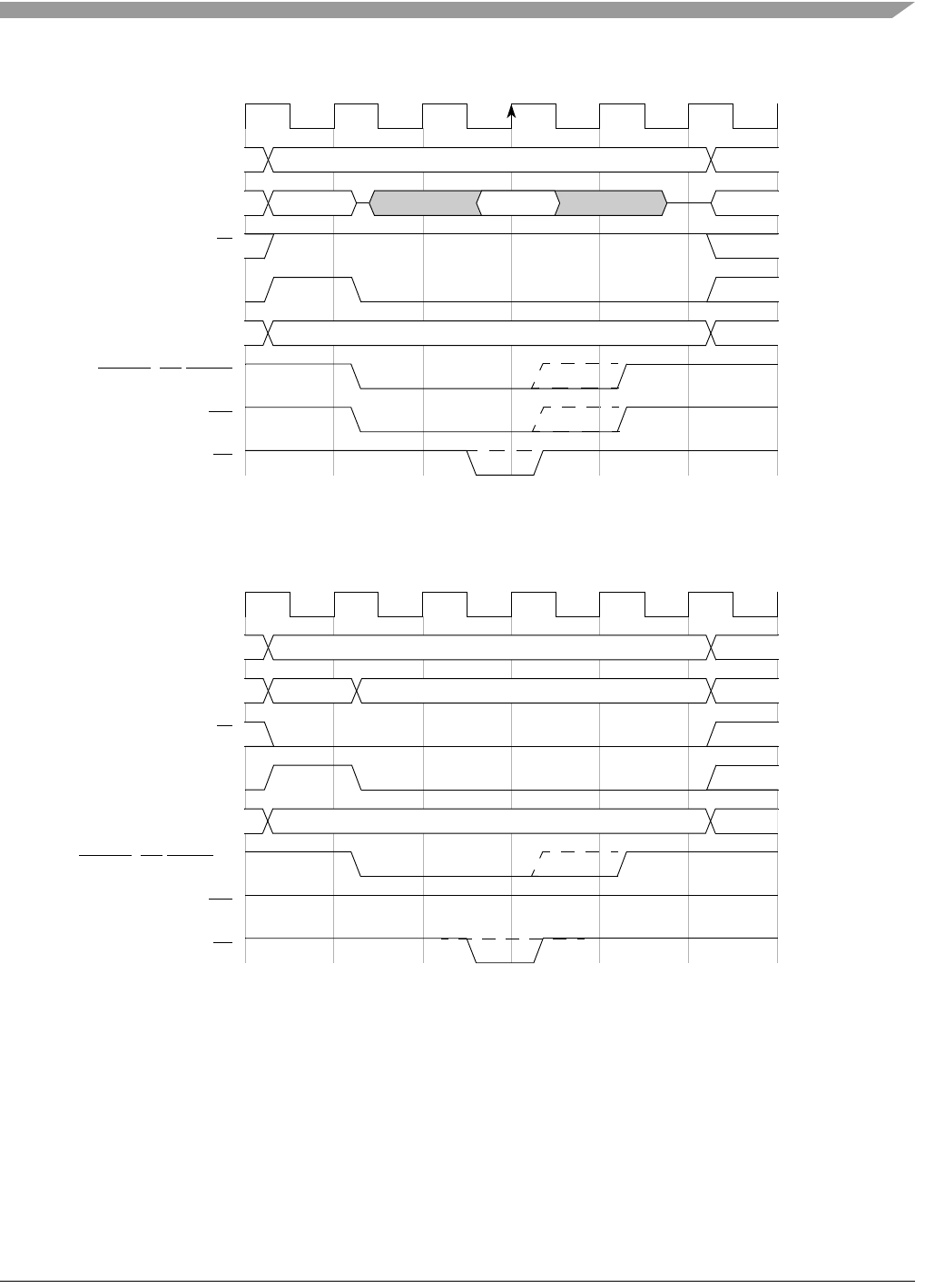
Functional Description
MCF548x Reference Manual, Rev. 3
Freescale Semiconductor 17-23
Figure 17-20. Read Bus Cycle (One Wait State)
Figure 17-21. Write Bus Cycle (One Wait State)
17.6.5.4.2 Address Setup and Hold
The timing of the assertion and negation of the chip selects, byte selects, and output enable can be
programmed on a chip select basis. Each chip select can be programmed to assert one to four clocks after
address latch enable (ALE) is asserted. Figure 17-22 and Figure 17-23 show read and write bus cycles with
two clocks of address setup.
CLK
AD[X:0]
AD[31:Y]
R/W
ALE
TA
OE
S0 S1 WS S2 S3
FBCSn, BE/BWEn
ADDR[X:0]
A[31:Y]DATA
TSIZ[1:0] TSIZ[1:0]
CLK
AD[X:0]
AD[31:Y]
R/W
ALE
TA
OE
S0 S1 WS S2 S3
FBCSn, BE/BWEn
ADDR[X:0]
A[31:Y]DATA
TSIZ[1:0] TSIZ[1:0]
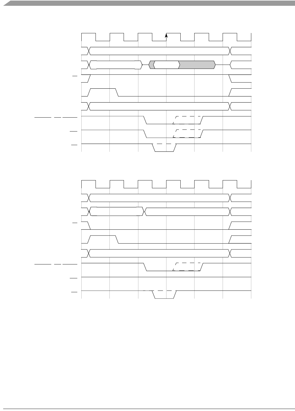
MCF548x Reference Manual, Rev. 3
17-24 Freescale Semiconductor
Figure 17-22. Read Bus Cycle with Two Clock Address Setup (No Wait States)
Figure 17-23. Write Bus Cycle with Two Clock Address Setup (No Wait States)
In addition to address setup, there is also a programmable address hold option for each chip select. Address
and attributes can be held one to four clocks after chip select, byte selects, and output enable negate.
Figure 17-24 and Figure 17-25 show read and write bus cycles with two clocks of address hold.
CLK
AD[X:0]
AD[31:Y]
R/W
ALE
TA
OE
S0 AS S1 S2 S3
FBCSn, BE/BWEn
ADDR[X:0]
A[31:Y]
TSIZ[1:0] TSIZ[1:0]
DATA
CLK
AD[X:0]
AD[31:Y]
R/W
ALE
TA
OE
S0 AS S1 S2 S3
FBCSn, BE/BWEn
ADDR[X:0]
DATA
TSIZ[1:0] TSIZ[1:0]
A[31:Y]
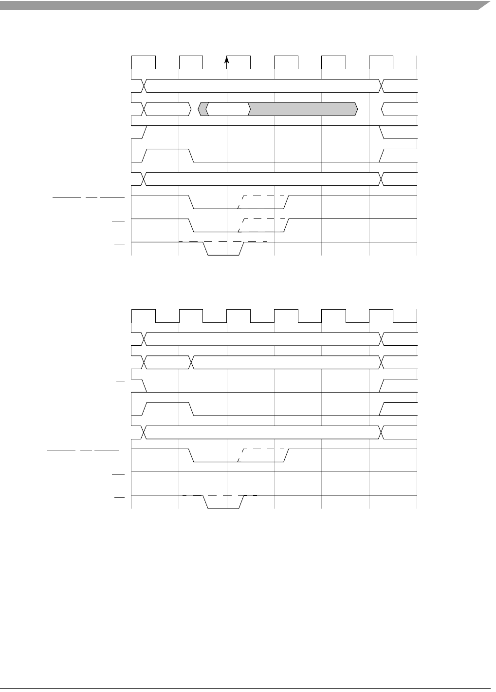
Functional Description
MCF548x Reference Manual, Rev. 3
Freescale Semiconductor 17-25
Figure 17-24. Read Cycle with Two Clock Address Hold (No Wait States)
Figure 17-25. Write Cycle with Two Clock Address Hold (No Wait States)
Figure 17-26 shows a bus cycle that uses address setup, wait states, and address hold.
CLK
AD[X:0]
AD[31:Y]
R/W
ALE
TA
OE
S0 S1 S2 S3 AH
FBCSn, BE/BWEn
ADDR[X:0]
A[31:Y]DATA
TSIZ[1:0] TSIZ[1:0]
CLK
AD[X:0]
AD[31:Y]
R/W
ALE
TA
OE
S0 S1 S2 S3 AH
FBCSn, BE/BWEn
ADDR[X:0]
A[31:Y]DATA
TSIZ[1:0] TSIZ[1:0]
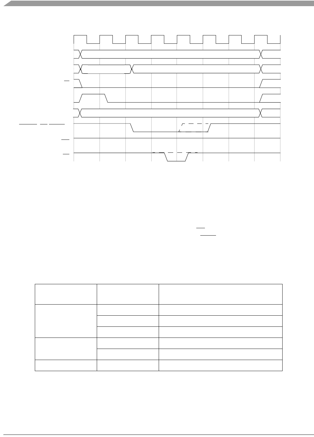
MCF548x Reference Manual, Rev. 3
17-26 Freescale Semiconductor
Figure 17-26. Write Cycle with Two Clock Address Setup and
Two Clock Hold (One Wait State)
17.6.6 Burst Cycles
The MCF548x can be programmed to initiate burst cycles if its transfer size exceeds the size of the port it
is transferring to. The initiation of a burst cycle is encoded on the size pins. For burst transfers to smaller
port sizes, TSIZ[1:0] indicate the size of the entire transfer. For example, with bursting enabled, a word
transfer to an 8-bit port would take a 2-byte burst cycle, for which TSIZ[1:0] = 10 throughout. A longword
transfer to an 8-bit port would take a 4-byte burst cycle, for which TSIZ[1:0] = 00 throughout.
With bursting disabled, any transfer is larger than port size is broken into multiple individual transfers.
With bursting enabled, an access is larger than port size would result a burst cycle of multiple beats.
Table 17-12 shows the result of such transfer translations.
The MCF548x bus can support 3-1-1-1 burst cycles and optimize DMA transfers. A user can add wait
states by delaying termination of the cycle. If internal termination is used, different wait state counters can
be used for the first access and the following beats.
Table 17-12. Transfer Size and Port Size Translation
Port Size PS[1:0] Transfer Size
TSIZ[1:0]
Burst-inhibited: number of transfers
Burst enabled: number of beats
01 (8-bit)
10 (word) 2
00 (longword) 4
11 (line) 16
1- (16-bit) 00 (longword) 2
11 (line) 8
00 (32-bit) 11 (line) 4
CLK
AD[X:0]
AD[31:Y]
R/W
ALE
TA
OE
S0 AS S1 WS S2 S3 AH
FBCSn, BE/BWEn
ADDR[X:0]
DATA
TSIZ[1:0] TSIZ[1:0]
A[31:Y]
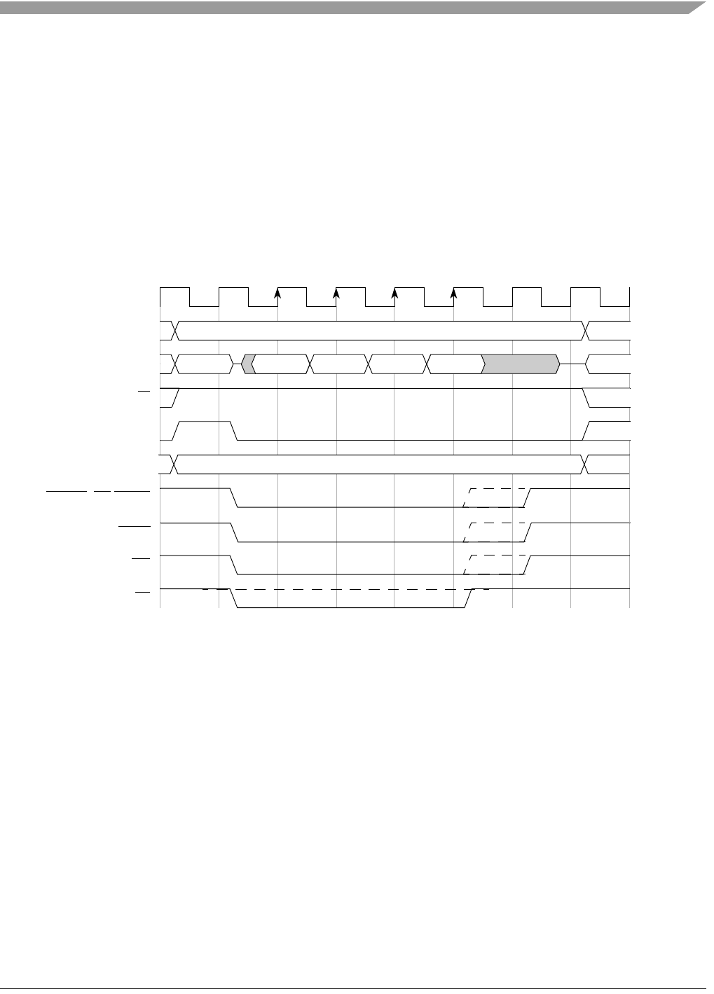
Functional Description
MCF548x Reference Manual, Rev. 3
Freescale Semiconductor 17-27
NOTE
Line-sized transfers requested by the core or cache are broken up into four
individual longword transfers, but the DMA can request line-sized transfers
when the read line or combine write flags are set. See Section 24.4.9, “Line
Buffers,” for more information.
CSCRs are used to enable bursting for reads, writes, or both. Memory spaces can be declared
burst-inhibited for reads and writes by clearing the appropriate CSCRn[BSTR,BSTW].
Figure 17-27 shows a longword read through an 8-bit device programmed for burst enable. The transfer
results in a 4-beat burst and the data is driven on AD[31:24]. Notice that the transfer size is driven at
longword (2’b00) throughout the bus cycle.
Figure 17-27. Longword Read Burst from 8-Bit Port 3-1-1-1 (No Wait States)
Figure 17-28 shows a longword write through an 8-bit device programmed for burst enable. The transfer
results in a 4-beat burst and the data is driven on AD[31:24]. Notice that the transfer size is driven at
longword (2’b00) throughout the bus cycle.
CLK
AD[23:0]
AD[31:24]
R/W
ALE
TA
OE
S0 S1 S2 S2 S2 S2 S3
FBCSn, BE/BWEn
ADDR[23:0]
A[31:24] DATA DATA DATA DATA
TSIZ[1:0] 00
TBST
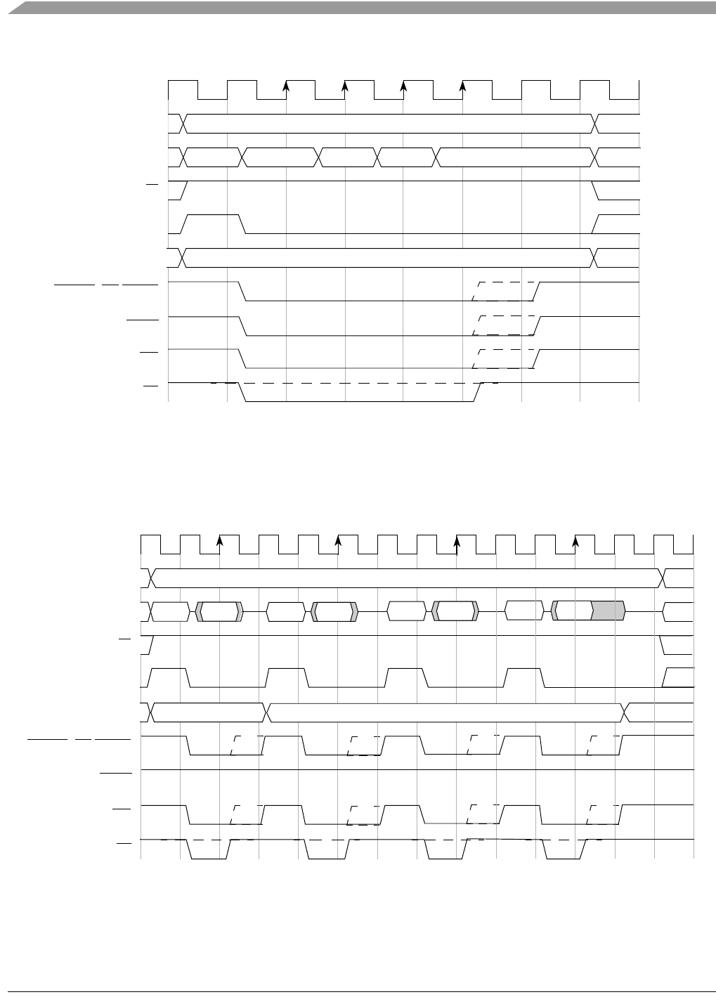
MCF548x Reference Manual, Rev. 3
17-28 Freescale Semiconductor
Figure 17-28. Longword Write Burst to 8-Bit Port 3-1-1-1 (No Wait States)
Figure 17-29 shows a longword read through an 8-bit device with burst inhibited. The transfer results in
four individual transfers. Notice that the transfer size is driven at longword (2’b00) during the first transfer
and at byte (2’b01) during the next three transfers.
Figure 17-29. Longword Read Burst-Inhibited from 8-Bit Port (No Wait States)
CLK
AD[23:0]
AD[31:24]
R/W
ALE
TA
OE
S0 S1 S2 S2 S2 S2 S3
FBCSn, BE/BWEn
ADDR[23:0]
TSIZ[1:0] 00
TBST
A[31:24] DATA DATA DATA DATA
CLK
AD[23:0]
AD[31:24]
R/W
ALE
TBST
S0 S1 S2 S2 S2
S2 S3
FBCSn, BE/BWEn
DATA
TSIZ[1:0]
TA
S0 S0
S1 S1 S1
S0
A[31:24] DATA A[31:24] A[31:24] A[31:24]
DATA DATA DATA
ADDR[23:0]
00
0101
OE
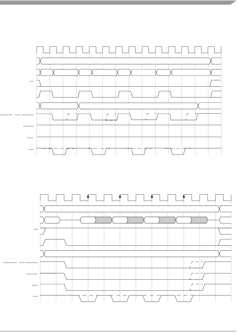
Functional Description
MCF548x Reference Manual, Rev. 3
Freescale Semiconductor 17-29
Figure 17-30 shows a longword write through an 8-bit device with burst inhibited. The transfer results in
four individual transfers. Notice that the transfer size is driven at longword (2’b00) during the first transfer
and at byte (2’b01) during the next three transfers.
Figure 17-30. Longword Write Burst-Inhibited to 8-Bit Port (No Wait States)
Figure 17-31 illustrates another read burst transfer, but in this case a wait state is added between individual
beats.
Figure 17-31. Longword Read Burst from 8-Bit Port 4-2-2-2 (One Wait State)
CLK
AD[23:0]
AD[31:24]
R/W
ALE
TBST
S0 S1 S2 S2 S2
S2 S3
F
BCSn, BE/BWEn
TSIZ[1:0]
TA
S0 S0
S1 S1 S1
S0
ADDR[23:0]
00
01
01
OE
A[31:24] A[31:24]
DATA A[31:24]
DATA A[31:24]
DATA
DATA
CLK
AD[23:0]
AD[31:24]
R/W
ALE
TA
OE
S0 S1 WS S2 WS/SWS S2 WS/SWS S2 WS/SWS S2 S3
FBCSn, BE/BWEn
ADDR[23:0]
A[31:24]
DATA DATA DATA DATA
TSIZ[1:0] 00
TBST
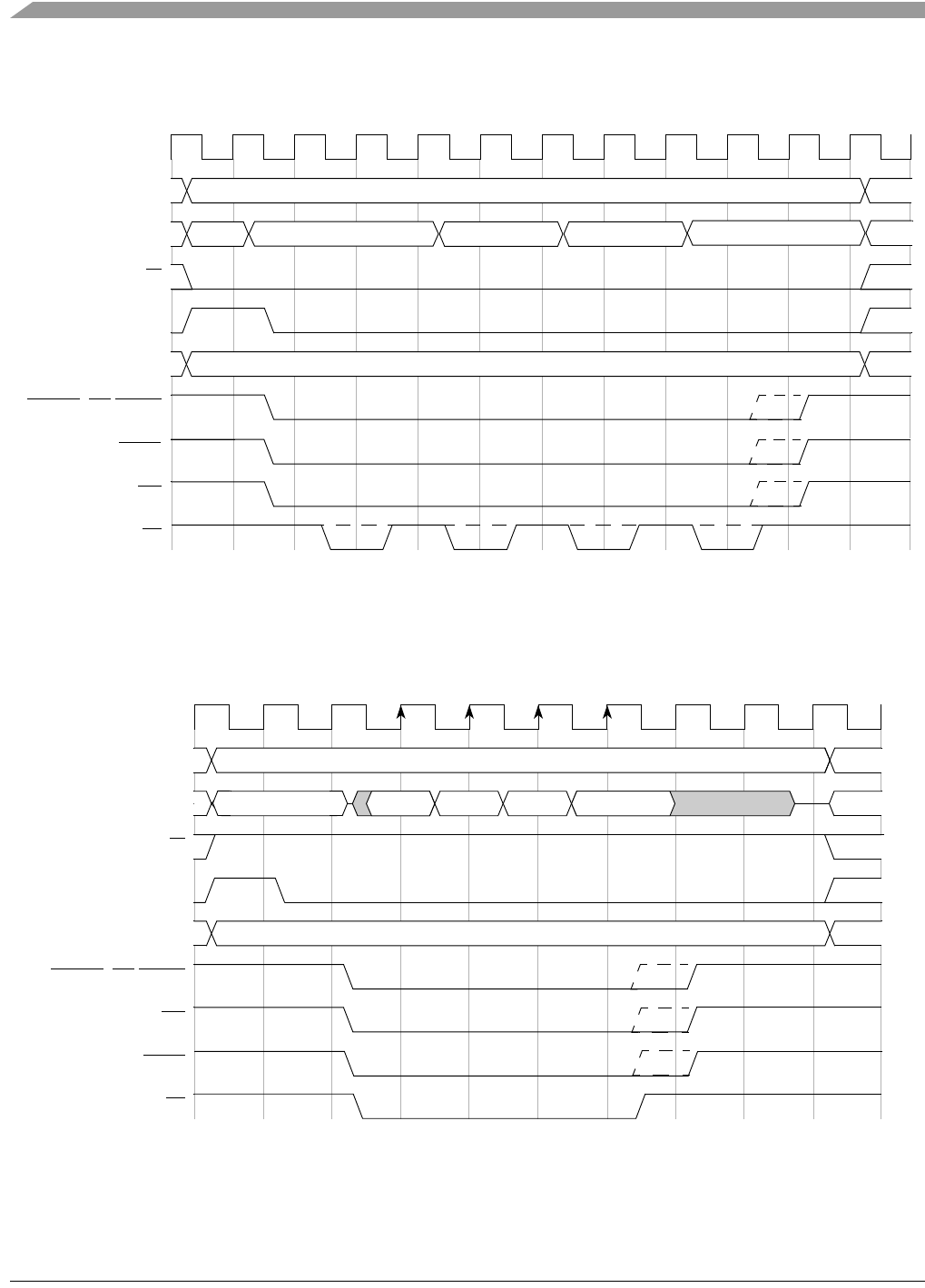
MCF548x Reference Manual, Rev. 3
17-30 Freescale Semiconductor
Figure 17-31 illustrates a write burst transfer with one wait state.
Figure 17-32. Longword Write Burst to 8-Bit Port 4-2-2-2 (One Wait State)
If address setup and hold are used, only the first and last beat of the burst cycle will be affected as shown
in Figure 17-33.
Figure 17-33. Longword Read Burst from 8-Bit Port 4-1-1-1 (Address Setup and Hold)
Figure 17-34 shows a write cycle with one clock of address setup and address hold.
CLK
AD[23:0]
AD[31:24]
R/W
ALE
TA
OE
S0 S1 WS S2 WS/SWS S2 WS/SWS S2 WS/SWS S2 S3
FBCSn, BE/BWEn
ADDR[23:0]
A[31:24]
DATA
TSIZ[1:0] 00
TBST
DATA DATA
DATA
CLK
AD[23:0]
AD[31:24]
R/W
ALE
TSIZ[1:0]
TA
TBST
S0 AS S1 S2 S2 S2 S2 S3 AH
OE
ADDR[23:0]
A[31:24] DATA DATA DATA DATA
FBCSn, BE/BWEn
11
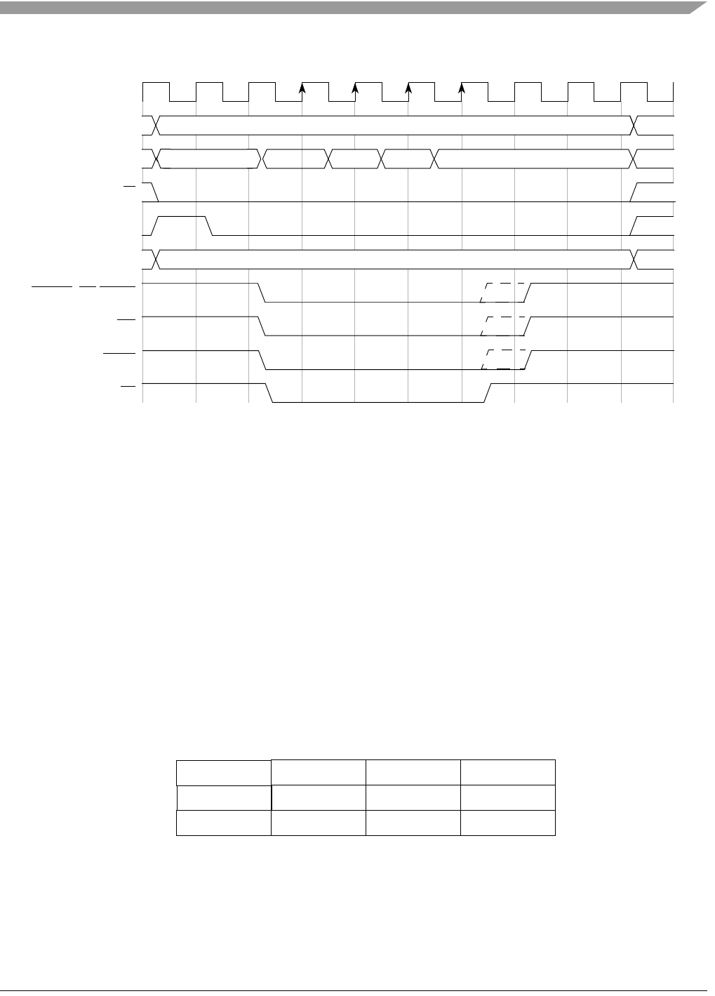
Functional Description
MCF548x Reference Manual, Rev. 3
Freescale Semiconductor 17-31
Figure 17-34. Longword Write Burst to 8-Bit Port 4-1-1-1 (Address Setup and Hold)
17.6.7 Misaligned Operands
Because operands, unlike opcodes, can reside at any byte boundary, they are allowed to be misaligned. A
byte operand is properly aligned at any address, a word operand is misaligned at an odd address, and a
longword is misaligned at an address not a multiple of four. Although the MCF548x enforces no alignment
restrictions for data operands (including program counter (PC) relative data addressing), additional bus
cycles are required for misaligned operands.
Instruction words and extension words (opcodes) must reside on word boundaries. Attempting to prefetch
a misaligned instruction word causes an address error exception.
The MCF548x converts misaligned, cache-inhibited operand accesses to multiple aligned accesses.
Figure 17-35 shows the transfer of a longword operand from a byte address to a 32-bit port. First a byte is
transferred at an offset of 0x1. The slave device supplies the byte and acknowledges the data transfer.
When the MCF548x starts the second cycle, a word is transferred with a byte offset of 0x2. The next two
bytes are transferred in this cycle. In the third cycle, byte 3 is transferred. The byte offset is now 0x0, the
port supplies the final byte, and the operation is complete.
Figure 17-35. Example of a Misaligned Longword Transfer (32-Bit Port)
If an operand is cacheable and is misaligned across a cache-line boundary, both lines are loaded into the
cache. The example in Figure 17-36 differs from the one in Figure 17-35 because the operand is
word-sized and the transfer takes only two bus cycles.
CLK
AD[23:0]
AD[31:24]
R/W
ALE
TSIZ[1:0]
TA
TBST
S0 AS S1 S2 S2 S2 S2 S3 AH
OE
ADDR[23:0]
A[31:24] DATA DATA DATA
FBCSn, BE/BWEn
11
DATA
–– Byte 0 –– ––
Transfer 1
–– –– Byte 1 Byte 2
Byte 3 –– –– ––
Transfer 2
Transfer 3
001
010
100
16 1531 024 23 78 A[2:0]

MCF548x Reference Manual, Rev. 3
17-32 Freescale Semiconductor
Figure 17-36. Example of a Misaligned Word Transfer (32-Bit Port)
17.6.8 Bus Errors
The MCF548x has no bus monitor. If the auto-acknowledge feature is not enabled for the address that
generates the error, the bus cycle can be terminated by asserting TA or by using the software watchdog
timer. If it is required that the MCF548x handle a bus error differently, an interrupt handler can be invoked
by asserting an interrupt to the core along with TA when the bus error occurs.
–– –– –– Byte 0Transfer 1
Byte 0 –– –– —Transfer 2
001
100
16 1531 024 23 78 A[2:0]

MCF548x Reference Manual, Rev. 3
Freescale Semiconductor 18-1
Chapter 18
SDRAM Controller (SDRAMC)
18.1 Introduction
This chapter describes configuration and operation of the synchronous DRAM (SDRAM) controller. It
begins with a general overview and includes a description of signals involved in SDRAM operations. The
remainder of the chapter describes the programming model and signal timing, as well as the command set
required for synchronous DRAM operations. It also includes examples that the designer can follow to
better understand how to configure the SDRAM controller for synchronous operations.
18.2 Overview
18.2.1 Features
The MCF548x SDRAM controller contains the following features:
• Supports a glueless interface to SDR and DDR SDRAMs
• 32-bit fixed memory port width
• 64-bit data bus interface to internal XLB 64-bit bus
• 32 bytes critical word first burst transfer
• Up to 13 row address lines, up to 12 column address lines, 2 bits of bank address, and a maximum
of four chip selects. The maximum row bits plus column bits can be less than or equal to 24.
• Supports up to 1 Gbyte of memory—13+11 or 12+12 bit RA+CA, 2 bit BA, four chip selects
• Minimum memory configuration of 8 Mbyte—11 bit row address (RA), 8 bit column address
(CA), 2 bit bank address (BA) and one chip select
• Supports page mode to maximize the data rate
• Supports sleep mode and self-refresh mode
• Error detect and parity check are not supported
18.2.2 Terminology
The following terminology is used in this chapter:
• SDRAM block: Any group of DRAM memories selected by one of the MCF548x SDCS[3:0]
signals. Thus, the MCF548x can support up to four independent memory blocks. The base address
of each block is programmed in the DRAM address and control registers (DACR0 and DACR1).
• SDRAM bank: An internal partition in an SDRAM device. For example, a 64-Mbit SDRAM
component might be configured as four 512K x 32 banks. Banks are selected through the
SD_BA[1:0] signals.
• SDRAM: These are RAMs that operate like asynchronous DRAMs but with a synchronous clock,
a pipelined, multiple-bank architecture, and a faster speed.
• Single data rate (SDR) SDRAM: This is SDRAM that drives/latches data and command
information on the rising edge of the clock.
• Double data rate (DDR) SDRAM: This is SDRAM that latches command information on the rising
edge of the clock, but data is driven/latched on both the rising and falling edges of the clock rather
than on just the rising edge. This doubles data throughput rate without an increase in frequency.
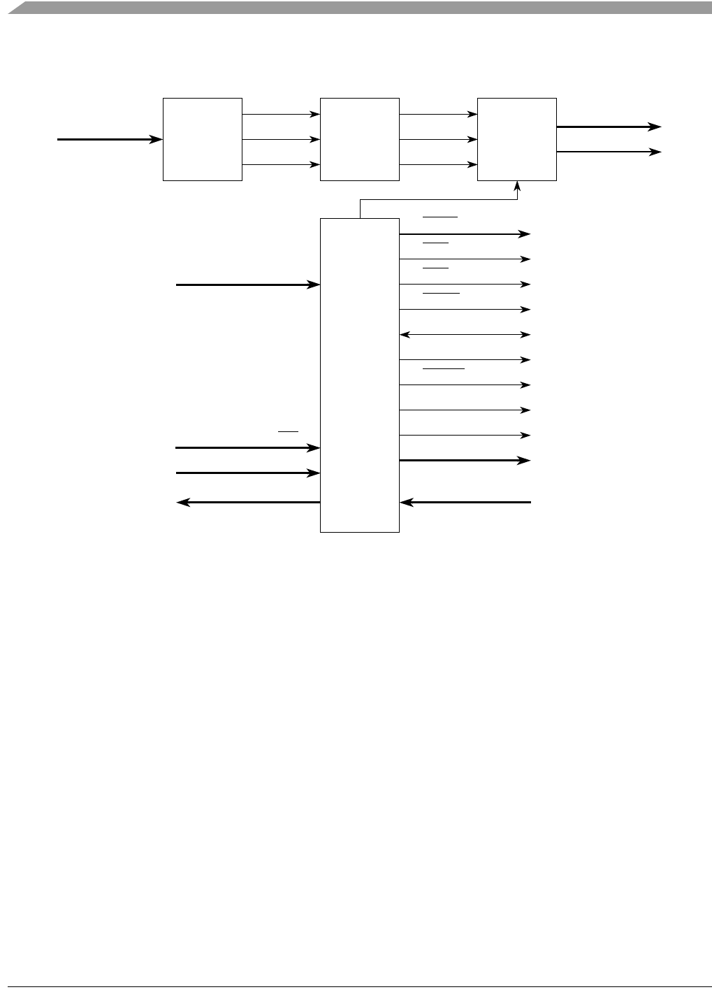
MCF548x Reference Manual, Rev. 3
18-2 Freescale Semiconductor
18.2.3 Block Diagram
Figure 18-1. SDRAM Controller Block Diagram
18.3 External Signal Description
18.3.1 SDRAM Data Bus (SDDATA[31:0])
SDDATA[31:0] is the bidirectional, non-multiplexed data bus used for SDRAM accesses. Data is sampled
by the MCF548x on the rising edge of SDCLK when in SDR mode, and on both the rising and falling edge
of SDCLK when in DDR mode.
18.3.2 SDRAM Address Bus (SDADDR[12:0])
The SDADDR[12:0] signals are the 13-bit, uni-directional address bus used for multiplexed row and
column addresses during SDRAM bus cycles. The address multiplexing supports up to 256 Mbytes of
SDRAM per chip select.
18.3.3 SDRAM Bank Addresses (SDBA[1:0])
Each SDRAM module has four internal row banks. The SDBA[1:0] signals are used to select the row bank.
It is also used to select the SDRAM internal mode register during power-up initialization.
addr[1:3] CAS
SDWE
SDDQS
SDCLK[1:0]
SDCLK[1:0]
SDCKE
RAS
SDCS[3:0]
dataout[63:0]
SDDM
SDDATA[31:0]
SDDATA[31:0]
Row
Bank
Column
addr[29:4]
Row
Bank
Column
SDBA[1:0]
SDADDR[12:0]
Select
datain[63:0]
SDRAM
Controller
State
Machine
Read Data
Buffer
Write Data
Buffer
Address
Output
MUX
Address
Pipeline
Latches
Address
Input
MUX
tsiz[1:0], tbst

External Signal Description
MCF548x Reference Manual, Rev. 3
Freescale Semiconductor 18-3
18.3.4 SDRAM Row Address Strobe (RAS)
This output is the SDRAM synchronous row address strobe.
18.3.5 SDRAM Column Address Strobe (CAS)
This output is the SDRAM synchronous column address strobe.
18.3.6 SDRAM Chip Selects (SDCS[3:0])
These signals interface to the chip select lines of the SDRAMs within a memory block. Thus, there is one
SDCS line for each memory block (the MCF548x supports up to four SDRAM memory blocks).
18.3.7 SDRAM Write Data Byte Mask (SDDM[3:0])
These output signals are sampled by the SDRAM on both edges of SDDQS to determine which byte lanes
of the SDRAM data bus should be latched during a write cycle. In DDR mode, these bits are ignored during
read operations.
18.3.8 SDRAM Data Strobe (SDDQS[3:0])
These bidirectional signals indicate when valid data is on the SDRAM data bus. Table 18-1 shows the
correspondence between SDDATA byte lanes and the SDDQS and SDDM signals.
18.3.9 SDRAM Clock (SDCLK[1:0])
This is the output clock for SDRAM accesses.
18.3.10 Inverted SDRAM Clock (SDCLK[1:0])
This is the inverted version of the SDRAM clock. It is used with SDCLK to provide the differential clocks
for DDR SDRAM.
18.3.11 SDRAM Write Enable (SDWE)
The SDRAM write enable (SDWE) is asserted to signify that a DRAM write cycle is underway. A read
cycle is indicated by the negation of SDWE.
Table 18-1. SDDQS and SDDM to Byte Lane Mapping
Byte Lane SDDQS SDDM
SDDATA[31:24] (MSB) SDDQS3 SDDM3
SDDATA[23:16] SDDQS2 SDDM2
SDDATA[15:8] SDDQS1 SDDM1
SDDATA[7:0] (LSB) SDDQS0 SDDM0

MCF548x Reference Manual, Rev. 3
18-4 Freescale Semiconductor
18.3.12 SDRAM Clock Enable (SDCKE)
This output is the SDRAM clock enable. SDCKE negates to put the SDRAM into low-power, self-refresh
mode.
18.3.13 SDR SDRAM Data Strobe (SDRDQS)
This is connected to SDDQS inputs. It is used in SDR mode only.
18.3.14 SDRAM Memory Supply (SDVDD)
These pins supply positive power to the SDRAM module. SDVDD should be connected to +2.5V for DDR
operation and +3.3V for SDR.
18.3.15 SDRAM Reference Voltage (VREF)
This is the input reference voltage for differential SSTL_2 inputs. It is used in both DDR and SDR modes.
For DDR VREF should be connected to 1.25V, and for SDR VREF should be connected to 1.5V.
18.4 Interface Recommendations
18.4.1 Supported Memory Configurations
The SDRAM controller supports up to 13 row addresses and up to 12 column addresses. However, the
maximum row and column addresses are not supported at the same time. The number of row and column
addresses must be less than or equal to 24. In addition to row/column address lines, there are always two
row bank address bits. Therefore, the greatest possible address space which can be accessed using a single
chip select is (226) x 32 bits, or 256 Mbytes.
Table 18-2 shows the address multiplexing used by the MCF548x for different configurations. When the
SDRAM controller receives the internal module enable, it latches the internal bus address lines addr[27:2]
and multiplexes them into row, column and row bank addresses. addr[9:2] are always used for CA[7:0],
addr[11:10] are always used for BA[1:0], and addr[23:12] are always used for RA[11:0]. addr[27:24] can
be used for additional row or column address bits, as needed.
NOTE
The SDRAMC only supports an external 32-bit data bus. It is not possible
to connect a smaller device(s) to only part of the SDRAM’s data bus. For
example, if 16-bit wide devices are used, then you must use two 16-bit
devices connected as a 32-bit port.

Interface Recommendations
MCF548x Reference Manual, Rev. 3
Freescale Semiconductor 18-5
All memory devices of a single chip select block must have the same configuration and row/col address
width; however, this is not necessary between different blocks. If mixing different memory organizations
in different blocks, the following guidelines will ensure that every block is fully contiguous.
• If all devices’ row address width is 12 bits, the column address can be ≥ 8 bits.
• If all devices’ row address width is 13 bits, the column address can be ≥ 8 bits.
• If all devices’ column address width is 8 bits, the row address can be ≥ 11 bits.
• x8 and x16 data width memory devices can be mixed (but not in the same space).
• x32 data width memory devices cannot be mixed with any other width.
Table 18-2. SDRAM Address Multiplexing
Device Configur
ation
Row bit x
Col bit x
Bank bit
Number
of
Devices
Total
Block
Size
SDCR
[MUX]
Setting
Internal Address
27 26 25 24 23–12 11–10 9–2
64 Mbits
512K x 32 bit 11 x 8 x 2 1 8 MB 00 — — — —
RA11-0 BA1-0 CA7-0
4M x 16 bit 12 x 8 x 2 2 16 MB 00 — — — —
8M x 8bit
12 x 9 x 2
432 MB
00 — — — CA8
13 x 8 x 2 01 — — — RA12
16M x 4 bit
12 x 10 x 2
864 MB
00 — — CA9 CA8
13 x 9 x 2 01 — — CA8 RA12
128
Mbits
4M x 32 bit 12 x 8 x 2 1 16 MB 00 — — — —
RA11-0 BA1-0 CA7-0
8M x 16 bit
12 x 9 x 2 232 MB
00 — — — CA8
13 x 8 x 2 01 — — — RA12
16M x 8 bit
12 x 10 x 2
464 MB
00 — — CA9 CA8
13 x 9 x 2 01 — — CA8 RA12
32M x 4 bit
12 x 11 x 2
8128
MB
00 — CA11 CA9 CA8
13 x 10 x 2 01 — CA9 CA8 RA12
256
Mbits
16M x 16 bit
12 x 10 x 2
264 MB
00 — — CA9 CA8
RA11-0 BA1-0 CA7-0
13 x 9 x 2 01 — — CA8 RA12
32M x 8 bit
12 x 11 x 2
4128
MB
00 — CA11 CA9 CA8
13 x 10 x 2 01 — CA9 CA8 RA12
64M x 4 bit
12 x 12 x 2
8256
MB
00 CA12 CA11 CA9 CA8
13 x 11 x 2 01 CA11 CA9 CA8 RA12
512
Mbits
32M x 16 bit
12 x 11 x 2
2128
MB
00 — CA11 CA9 CA8
RA11-0 BA1-0 CA7-0
13 x 10x 2 01 — CA9 CA8 RA12
64M x 8bit
12 x 12 x 2
4256
MB
00 CA12 CA11 CA9 CA8
13 x 11 x 2 01 CA11 CA9 CA8 RA12
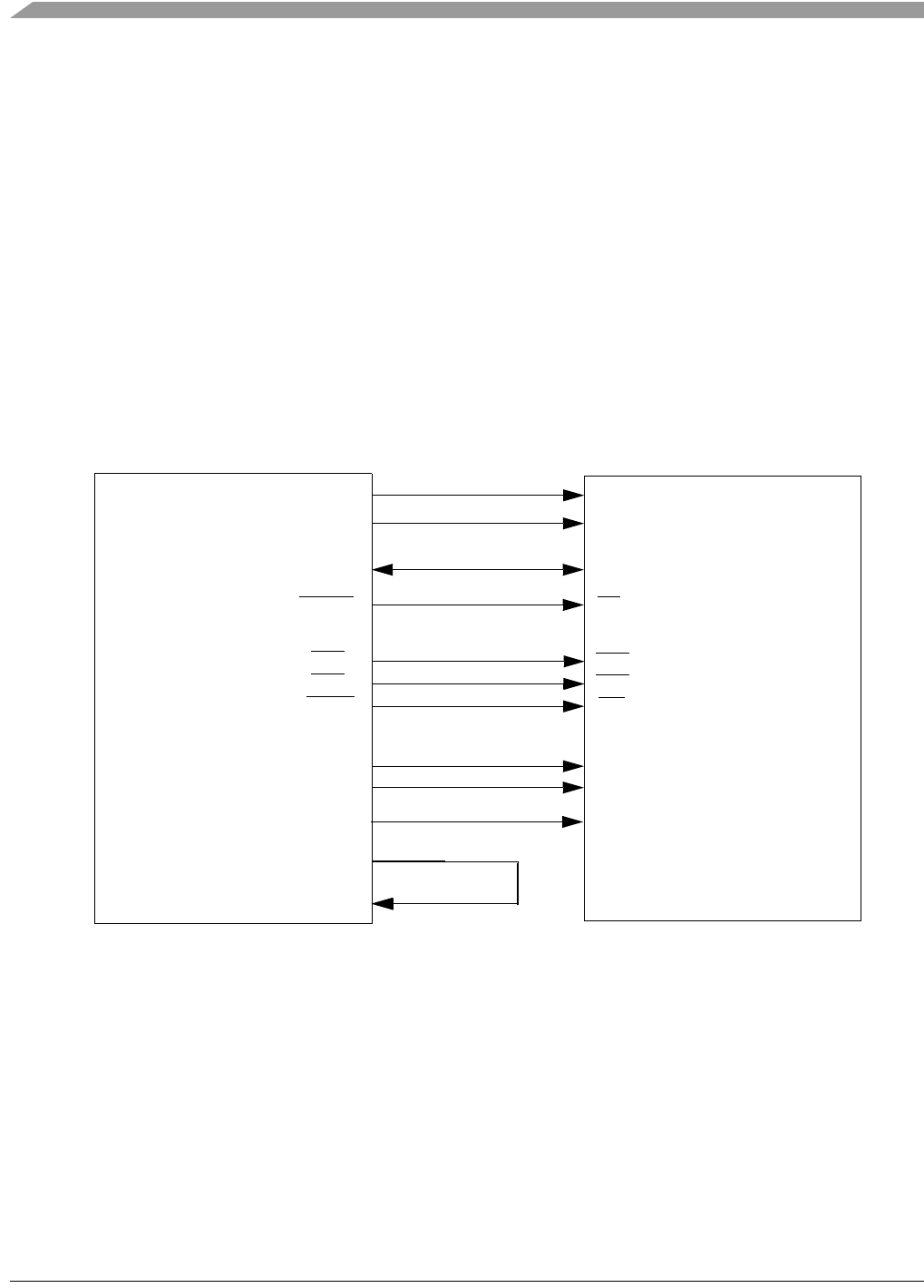
MCF548x Reference Manual, Rev. 3
18-6 Freescale Semiconductor
18.4.2 SDRAM SDR Connections
Figure 18-2 shows a block diagram of the connections between the MCF548x and SDR SDRAM
components. SDR design requires special timing consideration for the SDDQS[3:0] signals. For reads
from DDR SDRAMs, the memory will drive the DQS pins so that the data lines and DQS signals have
concurrent edges. The MCF548x SDRAMC is designed to latch data 1/4 clock after the SDDQS[3:0] edge.
For DDR SDRAM, this ensures that the latch time is in the middle of the data valid window.
The SDRAMC also uses the SDDQS[3:0] signals to determine when read data can be latched for SDR
SDRAM; however, SDR memories do not provide DQS outputs. Instead the SDRAMC provides an
SDRDQS output that is routed back into the controller as SDDQS[3:0]. The SDRDQS signal should be
routed such that the valid data from the SDRAM reaches the MCF548x at the same time or just before the
SDRDQS reaches the SDDQS[3:0] inputs. When routing SDRDQS the outbound trace length should be
matched to the SDCLK trace length. This will align SDRDQS to the SDCLK as if the memory had
generated the DQS pulse. The inbound trace should be routed along the data path. This should synchronize
the SDDQS so that the data is latched in the middle of the data valid window.
Figure 18-2. MCF548x Connections to SDR SDRAM
18.4.3 SDRAM DDR Component Connections
Figure 18-3 shows a block diagram of the connections between the MCF548x and DDR SDRAM
components.
MCF548X SDR SDRAM
SDADDR[12:0]
SDDATA[31:0]
SDBA[1:0]
SDCSn
RAS
CAS
SDWE
SDCKE
SDCLK[1:0] CLK
CKE
CS
RAS
CAS
WE
DQM[3:0]
BA[1:0]
A[12:0]
DQ[31:0]
SDDM[3:0]
SDRDQS
SDDQS[3:0]
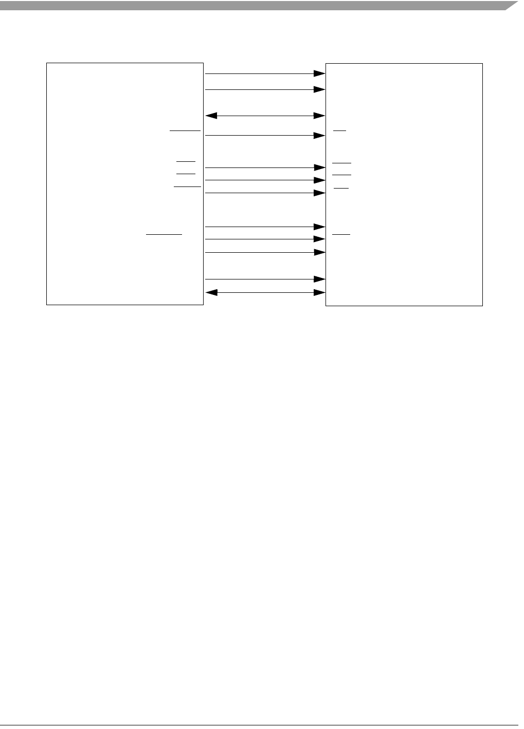
Interface Recommendations
MCF548x Reference Manual, Rev. 3
Freescale Semiconductor 18-7
Figure 18-3. MCF548x Connections to DDR SDRAM
18.4.4 SDRAM DDR DIMM Connections
There is a JEDEC standard for a 100-pin DDR DIMM with a 32-bit wide data bus. This DIMM standard
was designed specifically to support 32-bit processors. The MCF548x can support current DIMM
configurations up to 512 Mbytes.
Figure shows a block diagram of the connections between the MCF548x and DDR SDRAM DIMMs.
MCF548X DDR SDRAM
SD_CKE
SD_CLK[1:0]
SD_CLK[1:0]
SDDM[3:0]
SDDQS[3:0]
CLK
CLK
CKE
CS
RAS
CAS
WE
DM[3:0]
BA[1:0]
A[12:0]
DQ[31:0]
DQS[3:0]
SDADDR[12:0]
SDDATA[31:0]
SDBA[1:0]
SDCSn
RAS
CAS
SDWE
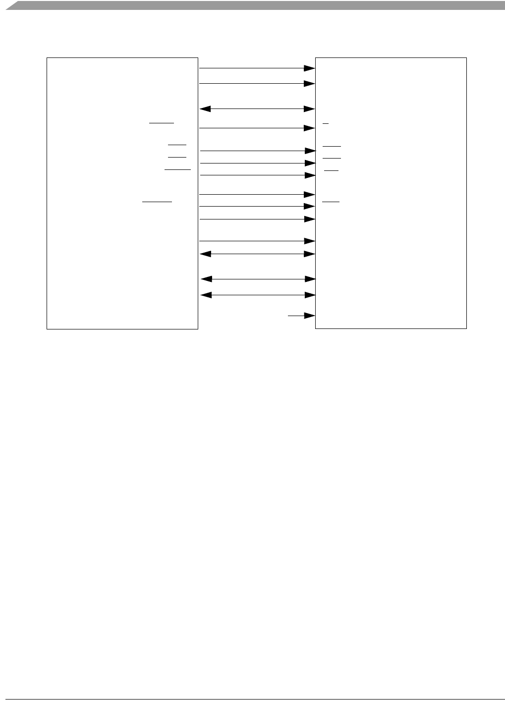
MCF548x Reference Manual, Rev. 3
18-8 Freescale Semiconductor
Figure 18-4. MCF548x Connections to 100-pin DDR SDRAM DIMM
18.4.5 DDR SDRAM Layout Considerations
Due to the critical timing for DDR SDRAM, there are a number of considerations that should be taken into
account during PCB layout:
• Minimize overall trace lengths.
• Each DQS, DM, and DQ group must have identical loading and similar routing to maintain timing
integrity.
• Control and clock signals are routed point-to-point.
• Trace length for clock, address, and command signals should match.
• Route DDR signals on layers adjacent to the ground plane.
• Use a VREF plane under the SDRAM.
• VREF is decoupled from both SDVDD and VSS.
• To avoid crosstalk, keep address and command signals separate from data and data strobes.
• Use different resistor packs for command/address and data/data strobes.
• Use single series, single parallel termination (25 Ω series, 50 Ω parallel values are recommended,
but standard resistor packs with similar values can be substituted).
• Series termination should be between the MCF548x and memory, but closest to the processor.
• The parallel termination at end of the signal line (close to the SDRAM).
• 0.1 uF decoupling for every termination resistor pack.
MCF548X DDR SDRAM
SDADDR[12:0]
SDDATA[31:0]
SDBA[1:0]
SDCS[1:0]
RAS
CAS
SDWE
SDCKE
SDCLK[1:0]
SDCLK[1:0]
SDDM[3:0]
SDDQS[3:0]
CLK[1:0]
CLK[1:0]
CKE
S[1:0]
RAS
CAS
WE
DM[3:0]
BA[1:0]
A[12:0]
DQ[31:0]
DQS[3:0]
SCL
SDA
SCL
SDA
SA0
SDVDD
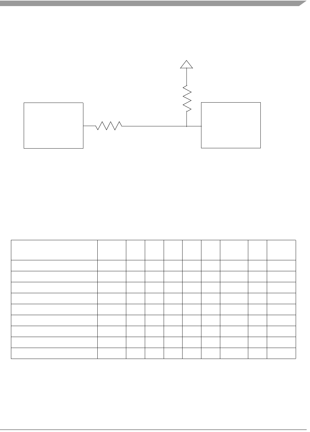
SDRAM Overview
MCF548x Reference Manual, Rev. 3
Freescale Semiconductor 18-9
18.4.5.1 Termination Example
Figure 18-5 shows the recommended termination circuitry for DDR SDRAM signals.
Figure 18-5. MCF548x DDR SDRAM Termination Circuit
18.5 SDRAM Overview
18.5.1 SDRAM Commands
When an internal bus master accesses SDRAM address space, the memory controller generates the
corresponding SDRAM command. Table 18-3 lists SDRAM commands supported by the memory
controller.
Table 18-3. SDRAM Commands
Function Symbol CKE CS RAS CAS WE BA[1:0] AP/C
MD Other A
Command Inhibit INH H H X X X X X X
No Operation NOP H L H H H X X X
Row and Bank Active ACTV H L L H H V V V
Read READ H L H L H V L V
Write WRITE H L H L L V L V
Precharge All Banks PALL H L L H L X H X
Load Mode Register LMRHLLLL LL V V
Load Extended Mode RegisterLEMRHLLLL LH V V
CBR Auto Refresh REF H L L L H X X X
MCF548X DDR SDRAM
VREF
25 Ω
50 Ω

MCF548x Reference Manual, Rev. 3
18-10 Freescale Semiconductor
Many commands require a delay before the next command may be issued; sometimes the delay depends
on the type of the next command. These delay requirements are managed by the values programmed in the
memory controller configuration registers (SDCFG1, SDCFG2).
18.5.1.1 Row and Bank Active Command (ACTV)
The ACTV command is responsible for latching the row and bank address and activating the specified row
in the memory array. Once the row is activated, it can be accessed using subsequent READ and WRITE
commands.
NOTE
The SDRAMC will support one active row for each chip select block. See
Section 18.6.1, “Page Management” for more information.
18.5.1.2 Read Command (READ)
When the SDRAMC receives a read request, it first checks the row and bank of the new access. If the
address falls within the active row of an active bank, it is a page hit, and the READ is issued as soon as
possible (pending any delays required by previous commands). If the address is within the active row, but
the needed bank is inactive, or if there is no active row, the memory controller will issue an ACTV
followed by the READ command. If the address is not within the active row, the memory controller will
issue a PALL command to close the active row. Then the SDRAMC issues ACTV to activate the necessary
bank and row for the new access, followed finally by the READ to the SDRAM.
The PALL and ACTV commands (if necessary) can sometimes be issued in parallel with an on-going data
movement.
All reads, whether burst or single, must be allowed to complete the entire burst length on the memory bus.
With SDR memory, the data masks are negated throughout the entire read burst length. With DDR
memory, the data masks are asserted throughout the entire read burst length; but DDR memory ignores the
data masks during reads.
18.5.1.3 Write Command (WRITE)
When the memory controller receives a write request, it first checks the row and bank of the new access.
If the address falls within the active row of an active bank, it is a page hit, and the WRITE is issued as soon
as possible (pending any delays required by previous commands). If the address is within the active row
but the needed bank is inactive, or if there is no active row, the memory controller will issue an ACTV
followed by the WRITE command. If the address is not within the active row, the memory controller will
Self-Refresh SREF H→LLLLH X X X
Power-Down PDWN H→LHXXX X X X
H = High
L = Low
V = Valid
X = Don’t care
Table 18-3. SDRAM Commands (Continued)
Function Symbol CKE CS RAS CAS WE BA[1:0] AP/C
MD Other A

SDRAM Overview
MCF548x Reference Manual, Rev. 3
Freescale Semiconductor 18-11
issue a PALL command to close the active row. Then the SDRAMC issues ACTV to activate the necessary
row and bank for the new access, followed finally by the WRITE command.
The PALL and ACTV commands (if necessary) can sometimes be issued in parallel with an on-going data
movement.
With both SDR and DDR memory, a read command can be issued overlapping the masked beats at the end
of a previous single write of the same SDCS; the read command aborts the remaining (unnecessary) write
beats. This is not possible with SDR memory, because SDR memory cannot be read with the masks
asserted.
18.5.1.4 Precharge All Banks Command (PALL)
The precharge command puts SDRAM into an idle state. The SDRAM must be in this idle state before a
REF, LMR, LEMR, or ACTV command to open a new row within a particular bank can be issued.
The memory controller issues the PALL command only when necessary for one of the following
conditions:
• Access to a new row
• Refresh interval elapsed
• Software commanded precharge
NOTE
The SDRAMC does not support the precharge selected bank memory
command.
18.5.1.5 Load Mode/Extended Mode Register Command (LMR, LEMR)
All SDRAM devices contain mode registers that are used to configure the timing and burst mode for the
SDRAM. These commands are used to access the mode registers that physically reside within the SDRAM
devices. During the LMR or LEMR command the SDRAM will latch the address bus and load the value
into the selected mode register.
NOTE
The LMR and LEMR commands are only used during SDRAM
initialization.
The following steps should be used to write the mode register and extended mode register:
1. Set the SDCR[MODE_EN] bit.
2. Write the SDMR[BA] bits to select the mode register.
3. Write the desired mode register value to the SDMR[ADDR]. Don’t overwrite the SDMR[BA]
values.
4. Set the SDMR[CMD] bit.
5. For DDR, repeat from step 2 for the extended mode register.
6. Clear the SDCR[MODE_EN] bit.

MCF548x Reference Manual, Rev. 3
18-12 Freescale Semiconductor
18.5.1.5.1 Mode Register Definition
Figure 18-6 shows the mode register definition. Note that this is the SDRAM’s mode register not the
SDRAMC’s mode/extended mode register (SDMR) defined in Section 18.7.3, “SDRAM Mode/Extended
Mode Register (SDMR).”
18.5.1.5.2 Extended Mode Register Definition
Figure 18-7 shows the extended mode register used by DDR SDRAMs. Note that this is the SDRAM’s
extended mode register, not the SDRAMC’s mode/extended mode register (SDMR) defined in
Section 18.7.3, “SDRAM Mode/Extended Mode Register (SDMR).”
BA1 BA0 A11 A10 A9 A8 A7 A6 A5 A4 A3 A2 A1 A0
Field 0 0 OP_MODE CASL BT BLEN
Figure 18-6. Mode Register
Table 18-4. Mode Register Field Descriptions
Address
Line Description
BA[1:0] Bank Address. These must both be zero to select the mode register.
A11–A7 Operating Mode.
00000 Normal Operation
00010 Reset DLL
Other values should not be used.
A6–A4 CAS latency. Delay in clocks from issuing a READ to valid data out. Check the SDRAM
manufacturer’s spec as the CASL settings supported can vary from memory to memory.
A3 Burst Type.
0 Sequential
1 Interleaved. This setting should not be used since the SDRAMC does not support interleaved
bursts.
A2–A0 Burst length. Determines the number of locations that are accessed for a single READ or
WRITE.
000 One. This is only a valid setting for SDR.
001 Two
010 Four
011 Eight (This value should be used for the MCF548x SDRAMC)
100–110 Reserved
111 Full page. This setting should not be used since full page bursting is not supported by the
SDRAMC.
BA1 BA0 A11 A10 A9 A8 A7 A6 A5 A4 A3 A2 A1 A0
Field 0 1 OPTION DLL
Figure 18-7. Extended Mode Register

SDRAM Overview
MCF548x Reference Manual, Rev. 3
Freescale Semiconductor 18-13
18.5.1.6 Auto Refresh Command (REF)
The memory controller issues auto refresh commands according to the SDCR[RC] value. Each time the
programmed refresh interval elapses, the memory controller issues a PALL command followed by a REF
command.
If a memory access is in progress at the time the refresh interval elapses, the memory controller schedules
the refresh after the transfer is finished; but the interval timer continues counting so that the average refresh
rate is constant.
After REF, the SDRAM is in an idle state and waits for an ACTV command.
18.5.1.7 Self-Refresh (SREF) and Power-Down (PDWN) Commands
The memory controller issues either a PDWN or a SREF command if the SDCR[CKE] bit is cleared. If
the SDCR[REF] bit is set when CKE is negated, the controller issues a SREF command; if the REF bit is
cleared, the controller issues a PDWN command. The REF bit may be changed in the same register write
that changes the CKE bit; the controller will act upon the new value of the REF bit.
Just like a REF, the controller automatically issues a PALL command before the self-refresh command.
The memory is reactivated from power-down or self-refresh mode by setting the CKE bit.
If a normal refresh interval elapses while the memory is in self-refresh mode, a PALL and REF will be
performed as soon as the memory is reactivated. If the memory is put into and brought out of self-refresh
all within a single refresh interval, the next automatic refresh will occur on schedule.
In self-refresh mode, the memory does not require an external clock. To restart periodic refresh when the
memory is reactivated, the REF bit must be reasserted. This can be done before the memory is reactivated,
or in the same control register write that sets CKE to exit self-refresh mode.
18.5.2 Power-Up Initialization
SDRAMs have a prescribed initialization sequence. The following sections detail the memory
initialization steps for both SDR and DDR SDRAM. The sequence might change slightly from
device-to-device. Refer to the device datasheet as the most relevant reference.
Table 18-5. Extended Mode Register Field Descriptions
Address
Line Description
BA[1:0] Bank Address.
00 Does not select the extended mode register
01 Selects the extended mode register
1x Reserved
A11–A1 Option. These bits are not defined by the DDR specification. Each DDR SDRAM manufacturer can use these
bits to implement optional features. Check with SDRAM manufacturer to determine if any optional features have
been implemented. For normal operation all bits should be cleared.
A0 Delay locked loop. Controls enabling of the delay locked loop circuitry used for DDR timing.
0 Enabled
1 Disabled.

MCF548x Reference Manual, Rev. 3
18-14 Freescale Semiconductor
18.5.2.1 SDR Initialization
SDR initialization requires the following steps:
1. After reset is deactivated, pause for the amount of time indicated in the SDRAM specification.
Usually 100µs or 200µs.
2. Initialize the SDRAM drive strength (SDRAMDS) and SDRAM chip select configuration
(CSnCFG) registers.
3. Program the SDRAM configuration registers (SDCFG1 and SDCFG2) with the correct delay and
timing values.
4. Issue a PALL command. Initialize the SDRAM control register (SDCR) with SDCR[IPALL] set.
The SDCR[MODE_EN, REF, and IREF] bits should all remain cleared for this step.
5. Refresh the SDRAM. The SDRAM spec should indicate a number of refresh cycles to be
performed before issuing an LMR command. Write to the SDCR with the IREF bit set
(SDCR[MODE_EN, REF, and IPALL] should be cleared). This will force a refresh of the
SDRAM each time the IREF bit is set. Repeat this step until the specified number of refresh
cycles have completed.
6. Set SDCR[REF] to enable automatic refreshing for the rest of the initialization and regular
operation. SDCR[MODE_EN, REF, and IPALL] remain cleared.
7. Initialize the SDRAM’s mode register using the LMR command. See Section 18.5.1.5, “Load
Mode/Extended Mode Register Command (LMR, LEMR)” for more instruction on issuing an
LMR command.
18.5.2.2 DDR Initialization
The steps for DDR initialization are similar to the SDR initialization sequence; however, there are some
additional steps required for DDR:
1. After reset is deactivated, pause for the amount of time indicated in the SDRAM specification.
Usually 100µs or 200µs.
2. Initialize the SDRAM drive strength (SDRAMDS) and SDRAM chip select configuration
(CSnCFG) registers.
3. Program the SDRAM configuration registers (SDCFG1 and SDCFG2) with the correct delay and
timing values.
4. Issue a PALL command. Initialize the SDRAM control register (SDCR) with SDCR[IPALL] set.
The SDCR[REF, and IREF] bits should remain cleared for this step.
5. Initialize the SDRAM’s extended mode register to enable the DLL. See Section 18.5.1.5, “Load
Mode/Extended Mode Register Command (LMR, LEMR)” for instructions on issuing an LEMR
command.
6. Initialize the SDRAM’s mode register and reset the DLL using the LMR command. See
Section 18.5.1.5, “Load Mode/Extended Mode Register Command (LMR, LEMR)” for more
instruction on issuing an LMR command. During this step the OP_MODE field of the mode
register should be set to “normal operation/reset DLL.”
7. Pause for the DLL lock time specified by the memory.

Functional Overview
MCF548x Reference Manual, Rev. 3
Freescale Semiconductor 18-15
8. Issue a second PALL command. Initialize the SDRAM control register (SDCR) with
SDCR[IPALL] set. The SDCR[REF, and IREF] bits should remain cleared for this step.
9. Refresh the SDRAM. The SDRAM spec should indicate a number of refresh cycles to be
performed before issuing an LMR command. Write to the SDCR with the IREF bit set
(SDCR[MODE_EN, REF, and IPALL] should be cleared). This will force a refresh of the
SDRAM each time the IREF bit is set. Repeat this step until the specified number of refresh
cycles have been completed.
10. Initialize the SDRAM’s mode register using the LMR command. See Section 18.5.1.5, “Load
Mode/Extended Mode Register Command (LMR, LEMR)” for more instruction on issuing an
LMR command. During this step the OP_MODE field of the mode register should be set to
“normal operation.”
11. Set SDCR[REF] to enable automatic refreshing, and clear SDCR[MODE_EN] to lock the SDMR.
SDCR[MODE_EN, IREF, and IPALL] remain cleared.
18.6 Functional Overview
18.6.1 Page Management
SDRAM devices have four internal banks. A particular row and bank of memory must be activated to
allow read and write accesses. The SDRAM controller supports paging mode to maximize the memory
access throughput. During operation, the SDRAM controller maintains an open page address for each
SDCS block. An open page is composed of the active rows in the internal banks.
SDRAMs can have a different row address open in each bank, but the SDRAMC does not support this.
The page size of a SDCS block is equal to the space size divided by the number of rows; but the page may
not be contiguous in the XLB address space because the internal address bits used for memory column
address [11:8] and column address [7:0] are not consecutive.
Because the column address may be split across two portions of the XLB address, the contiguous page size
is (number of banks) × (256 columns) × (number of bits). This gives a contiguous page size of 4 Kbytes.
However, the total (possibly fragmented) page size is (number of banks) × (number of columns) × (number
of bits).
If a new access does not fall in the open page of a SDCS block, the open page must be closed (PALL) and
the new page must be opened (ACTV), then the READ or WRITE command can proceed. An ACTV
command only activates one bank of a page. If another read or write falls in an inactive bank of the open
page, another ACTV is needed but no precharge is needed. If a read or write falls in any of the active banks
of the open page, no PALL or ACTV is needed; the read or write command can be issued immediately.
A page is kept open until one of the following conditions occurs:
• an access outside the open page
• a refresh cycle is started.
All SDCS blocks are refreshed at the same time; the refresh closes all banks of every SDRAM block.
18.6.2 Transfer Size
In the MCF548x, the internal data bus is 64 bits wide, while the SDRAM external interface bus is 32 bits
wide. Therefore, each XLB data beat requires two memory data beats. The SDRAM controller manages
the size translation (packing/unpacking) between 64- and 32-bit buses.

MCF548x Reference Manual, Rev. 3
18-16 Freescale Semiconductor
The SDRAM controller supports all possible XLB transfer sizes. SDRAMs are “burst only” devices;
unnecessary beats on the memory bus are masked (write) or discarded (read).
The SDRAMC will perform line bursts (32 byte) for all SDRAM access. This requires two beats of 16
bytes on the XLB, or eight beats of 4 bytes (one longword) on the memory bus. The SDRAM controller
transfers the critical longword first, followed by the next three sequential longwords.
The burst size and transfer order must be programmed in the SDRAM mode registers during initialization
(SDMR); the burst size also must be programmed in the memory controller (SDCFG2).
In a write operation, the data masks, SDDM[3:0], are used to inhibit writing unused bytes of each beat. In
a read operation, the excess read data is discarded.
18.7 Memory Map/Register Definition
The SDRAM controller contains four programming registers.
Table 18-6. SDRAMC Memory Map
Address
(MBAR +) Name Byte0 Byte1 Byte2 Byte3 Access
SDRAM Chip Select and Drive Strength Registers
0x04 SDRAM Drive Strength Register SDRAMDS R/W
0x20 SDRAM Chip Select 0 Configuration CS0CFG R/W
0x24 SDRAM Chip Select 1 Configuration CS1CFG R/W
0x28 SDRAM Chip Select 2 Configuration CS2CFG R/W
0x2C SDRAM Chip Select 3 Configuration CS3CFG R/W
SDRAMC Configuration Registers
0x0100 SDRAM Mode/Extended Mode Register SDMR R/W
0x0104 SDRAM Control Register SDCR R/W
0x0108 SDRAM Configuration Register 1 SDCFG1 R/W
0x010C SDRAM Configuration Register 2 SDCFG2 R/W

Memory Map/Register Definition
MCF548x Reference Manual, Rev. 3
Freescale Semiconductor 18-17
18.7.1 SDRAM Drive Strength Register (SDRAMDS)
31 30 29 28 27 26 25 24 23 22 21 20 19 18 17 16
R0 0 0000000000 0 0 0 0
W
Reset0 0 0000000000 0 0 0 0
15 14 13 1211 10 9 8 7654 3 2 1 0
R0 0 0 0 0 0 SB_E SB_C SB_A SB_S SB_D
W
Reset0 0 0000111111 1 1 1 1
Reg
Addr
MBAR + 0x04
Figure 18-8. SDRAM Drive Strength Register (SDRAMDS)
Table 18-7. SDRAMDS Field Descriptions
Bits Name Description
31–10 — Reserved. Should be cleared
9–8 SB_E Controls the drive strength of SDCKE. See Table 18-8 for encodings.
7–6 SB_C Controls the drive strength of SDRAM clocks. See Table 18-8 for encodings.
5–4 SB_A Controls the drive strength of SDCS[3:0], RAS, CAS, SDWE, SDADDR[12:0], and
SDBA[1:0]. See Table 18-8 for encodings.
3–2 SB_S Controls the drive strength of SDRDQS. See Table 18-8 for encodings.
1–0 SB_D Controls the drive strength of SDDATA[31:0], SDDM[3:0], and SDQS[3:0]. See
Table 18-8 for encodings.
Table 18-8. SDRAM Drive Strength Bit Encodings
SB_x[1:0] SD_VDD1
13.3V is for SDR mode, 2.5V is for DDR mode
Drive
10 3.3 8mA; SSTL_3 Class I
01 3.3 16mA; SSTL_3 Class II
00 3.3 24mA; SSTL_3
10 2.5 7.6mA; SSTL_2 Class I
01 2.5 13mA
00 2.5 15mA; SSTL_2 Class II
11 X No Drive;Hi-Z

MCF548x Reference Manual, Rev. 3
18-18 Freescale Semiconductor
18.7.2 SDRAM Chip Select Configuration Registers (CSnCFG)
Any chip select can be enabled or disabled, independent of others. Any chip select can be allocated any
size of address space from 1 Mbyte to 4 Gbyte, independent of others. Any chip select address space can
begin at any size-aligned base address, independent of others.
For contiguous memory with different sizes of mem banks, place largest bank at lowest address, then place
smaller banks in descending size order at ascending base address.
For example, assume CS0 = 16M, CS1 = empty, CS2 = 64M, CS3 = 64M, CS4 = 256M, CS5 = empty:
CS0CFG = 98000017 = enable 16M @ 0x9800 0000-0x98FF FFFF
CS1CFG = 00000000 = disable
CS2CFG = 90000019 = 64M @ 0x9000 0000-0x93FF FFFF
31 30 29 28 27 26 25 24 23 22 21 20 19 18 17 16
R CSBA 0 0 0 0
W
Reset0 00000000000 0 0 0 0
151413121110987654 3 2 1 0
R00 000000000 CSSZ
W
Reset0 00000000000 0 0 0 0
Reg
Addr
MBAR + 0x20 (CS0CFG), 0x24 (CS1CFG), 0x28 (CS2CFG), 0x2C (CS3CFG)
Figure 18-9. SRAM Chip Select Configuration Register (CSnCFG)
Table 18-9. CFnCFG Field Descriptions
Bits Name Description
31–20 CSBA Chip select base address.
19–5 — Reserved. Should be cleared.
4–0 CSSZ Chip select size.
00000 Disabled
00001–10010 Reserved
10011 1 Mbyte, compare A[31:20]
10100 2 Mbyte, compare A[31:21]
10101 4 Mbyte, compare A[31:22]
10110 8 Mbyte, compare A[31:23]
10111 16 Mbyte, compare A[31:24]
11000 32 Mbyte, compare A[31:25]
11001 64 Mbyte, compare A[31:26]
11010 128 Mbyte, compare A[31:27]
11011 256 Mbyte, compare A[31:28]
11100 512 Mbyte, compare A[31:29]
11101 1 Gbyte, compare A[31:30]
11110 2 Gbyte, compare A31
11111 4 Gbyte, ignore A[31:20]

Memory Map/Register Definition
MCF548x Reference Manual, Rev. 3
Freescale Semiconductor 18-19
CS3CFG = 94000019 = 64M @ 0x9400 0000-0x97FF FFFF
CS4CFG = 8000001b = 256M @ 0x8000 0000-0x8FFF FFFF
CS5CFG = 00000000 = disable
This gives 400 Mbyte total memory, at 0x8000 0000-0x98FF FFFF
18.7.3 SDRAM Mode/Extended Mode Register (SDMR)
The SDMR, shown in Figure 18-10, is used to write to the mode and extended mode registers that
physically reside within in the SDRAM chips. These registers must be programmed during SDRAM
initialization. See Section 18.5.2, “Power-Up Initialization” for more information on the initialization
sequence.
31 30 29 28 27 26 25 24 23 22 21 20 19 18 17 16
R BNKAD AD 0 CMD
W
Reset Uninitialized
1514131211109876543210
R0000000000000000
W
Reset0000000000000000
Reg
Addr
MBAR +0x0100
Figure 18-10. SDRAM Mode/Extended Mode Register (SDMR)
Table 18-10. SDMR Field Descriptions
Bits Name Description
31–30 BNKAD Bank address. Driven onto SDBA[1:0] along with a LMR/LEMR command. All SDRAM chip
selects are asserted simultaneously. SDCR[CKE] must be set before attempting to
generate an LMR/LEMR command. The SDBA[1:0] value is used to select between LMR
and LEMR commands.
00 Load mode register command (LMR)
01 Load extended mode register command (LEMR)
10–11 Reserved
29–18 AD Address. Driven onto SDADDR[11:0] along with an LMR/LEMR command. The AD value
is stored as the mode (or extended mode) register data.
17 — Reserved. Should be cleared.
16 CMD Command.
1 Generate an LMR/LEMR command
0 Do not generate any command
15–0 — Reserved. Should be cleared.

MCF548x Reference Manual, Rev. 3
18-20 Freescale Semiconductor
18.7.4 SDRAM Control Register (SDCR)
The SDCR, shown in Figure 18-11, controls SDRAMC operating modes including the refresh count and
address line muxing.
31 30 29 28 27 26 25 24 23 22 21 20 19 18 17 16
RMODE
_EN
CKE DDR REF 0 0 MUX AP DRIV
E
RCNT
W
Reset Uninitialized
1514131211109876543210
R 0 0 0 0 DQS_OE 0 0 0 BUFF 0 IREF IPALL 0
W
Reset Uninitialized
Reg
Addr
MBAR + 0x0104
Figure 18-11. SDRAM Control Register (SDCR)
Table 18-11. SDCR Field Descriptions
Bits Name Description
31 MODE_EN Mode enable.
0 Mode register locked, cannot be written
1 Mode register enabled, can be written
30 CKE Clock enable.
0 SDCKE is negated (low)
1 SDCKE is asserted (high)
29 DDR DDR mode select.
0 SDR mode
1 DDR mode
28 REF Refresh enable.
0 Automatic refresh disabled
1 Automatic refresh enabled
27–26 — Reserved. Should be cleared.
25–24 MUX Muxing control. Selects routing of addr[7:4] as row or column address bits as shown in Table 18-2.
23 AP Auto precharge control bit.
0 CA10 is the auto precharge control bit
1 Reserved

Memory Map/Register Definition
MCF548x Reference Manual, Rev. 3
Freescale Semiconductor 18-21
18.7.5 SDRAM Configuration Register 1 (SDCFG1)
The 32-bit read/write SDRAM configuration register 1 (SDCFG1) stores delay values necessary between
specific SDRAM commands. During initialization, software loads values to the register according to the
selected SDCLK frequency and SDRAM specifications. This register is reset only by a power-up reset
signal.
The read and write latency fields govern the relative timing of commands and data, and must be exact
values. All other fields govern the relative timing from one command to another, they have minimum
values but any larger value is also legal (but with decreased performance).
22 DRIVE Drive rule selection.
0 Tri-state except to write. SDDATA and SDDQS are only driven when necessary to perform a
write.
1 Drive except to read. SDDATA and SDDQS are only tristated when necessary to perform a
read. When not being driven for a write cycle, SDDATA hold the most recent value and SDDQS
are driven low.
This mode is intended for minimal applications only, to prevent floating signals and allow
unterminated board traces. However, terminated wiring is always recommended over
unterminated.
21–16 RCNT Refresh Count. Controls automatic refresh frequency. The number of bus clocks between refresh
cycles is (RC + 1) x 64.
RCNT = (tREFI/ (SDCLK x 64)) - 1, rounded down to the next integer value.
15–12 — Reserved. Should be cleared.
11–8 DQS_OE DQS output enable. Each DQS_OE bit is a master enable for the corresponding SDDQSn signal.
1 SDDQSn can drive as necessary, depending on commands and SDCR[DRIVE] setting.
0 SDDQSn can never drive. Use this value in SDR mode or in DDR mode with a “single DQS”
memory. Some 32-bit DDR devices only have a single DQS pin. Enable one of the SDDQSn
signals and disable the other three. Then short all 4 pins external to the part.
7–5 — Reserved. Should be cleared.
4 BUFF Buffering mode. Selects between buffered and unbuffered memory timing. Buffered and
unbuffered memory cannot be mixed.
1 System uses “buffered” memory modules.
0 System does not use “buffered” memory modules.
3 — Reserved. Should be cleared.
2 IREF Initiate Refresh (REF) command. Used to force a software initiated Refresh command.
1 Generate a Refresh command. All SDCSn signals are asserted simultaneously.
SDCR[CLK_EN] must be set before attempting to generate a software refresh command.
0 Do not generate a Refresh command.
1 IPALL Initiate Precharge All command. Used to force a software initiated PALL command.
1 Generate a PALL command. All SDCSn signals are asserted simultaneously. SDCR[CKE] must
be set before attempting to generate a software PALL command.
0 Do not generate a PALL command.
0 — Reserved. Should be cleared.
Table 18-11. SDCR Field Descriptions (Continued)
Bits Name Description

MCF548x Reference Manual, Rev. 3
18-22 Freescale Semiconductor
The minimum values of certain fields can be different for SDR and DDR SDRAM, even if the data sheet
timing is the same, because:
• In SDR mode, the memory controller counts the delay in SDCLK
• In DDR mode, the memory controller counts the delay in SDCLK × 2
SDCLK—memory controller clock—is the speed of the SDRAM interface and is equal to the internal bus
clock.
SDCLK × 2—double frequency of SDCLK—DDR uses both edges of the bus-frequency clock (SDCLK)
to read/write data
31 30 29 28 27 26 25 24 23 22 21 20 19 18 17 16
R SRD2RW 0 SWT2RD RDLAT 0 ACT2RW
W
Reset Uninitialized
15 14 13 12 11 10 9 8 7 6 5 4 3 2 1 0
R 0 PRE2ACT REF2ACT 0 WTLAT 0 0 0 0
W
Reset Uninitialized
Reg
Addr
MBAR + 0x0108
Figure 18-12. SDRAM Configuration Register 1 (SDCFG1)
Table 18-12. SDCFG1 Field Descriptions
Bits Name Description
31–28 SRD2RW Single Read to Read/Write/Precharge delay. Limiting case is usually Write to Precharge.
DDR mode:
SRD2RW = CASL + (BL/2) + 1
For DDR, suggested value = 0x7
SDR mode:
SRD2RW = CASL + BL + 1
If CASL=2, suggested value = 0xB
If CASL=3, suggested value = 0xC
27 — Reserved. should be cleared
26–24 SWT2RD Single Write to Read/Write/Precharge delay. Limiting case is Write to Precharge.
DDR mode:
SWT2RD = tWR/SDCLK + 1, suggested value = 0x3
SDR mode:
SWT2RD = tWR, suggested value = 0x2
23–20 RDLAT Read CAS Latency. Read latency. Read command to read data available delay counter.
DDR mode:
If CASL = 2, write 0x6
If CASL = 2.5, write 0x7
SDR mode:
If CASL = 2, write 0x2
If CASL = 3, write 0x3
Note: CASL=2.5 is not supported for SDR.

Memory Map/Register Definition
MCF548x Reference Manual, Rev. 3
Freescale Semiconductor 18-23
18.7.6 SDRAM Configuration Register 2 (SDCFG2)
The 32-bit read/write configuration register 2 stores delay values necessary between specific SDRAM
commands. During initialization, software loads values to the register according to the SDRAM
information obtained from the data sheet. This register is reset only by a power-up reset signal.
The burst length (BL) field must be exact. All other fields govern the relative timing from one command
to another, they have minimum values, but any larger value is also legal (but with decreased performance).
All delays in this register are expressed in SDCLK.
19 — Reserved. Should be cleared.
18–16 ACT2RW Active to Read/Write delay. Active command to any following read or write delay counter.
Suggested value = tRCD/SDCLK - 1 (Round up to nearest integer)
EXAMPLE: If tRCD = 20ns and SDCLK = 99 MHz
20ns / 10.1 ns = 1.98; round to 2; write 0x1.
Note: Count value is in SDCLK periods for both SDR and DDR mode.
15 — Reserved. Should be cleared.
14–12 PRE2ACT Precharge to Active delay. Precharge command to following Active command delay counter.
Suggested value = tRP/SDCLK - 1 (Round up to nearest integer)
EXAMPLE: If tRP = 20ns and SDCLK = 99MHz
20ns / 10.1ns = 1.98; round to 2; write 0x1.
Note: Count value is in SDCLK periods for both SDR and DDR mode.
11–8 REF2ACT Refresh to Active delay. Refresh command to following Active or Refresh command delay counter.
Suggested value = tRFC/SDCLK - 1 (Round up to nearest integer)
EXAMPLE: If tRFC = 75ns and SDCLK = 99MHz
75ns / 10.1ns = 7.425; round to 8; write 0x7.
Note: Count value is in SDCLK periods for both SDR and DDR mode.
7 — Reserved. Should be cleared.
6–4 WTLAT Write latency. Write command to write data delay counter.
For DDR, write 0x3
For SDR, write 0x0
3–0 — Reserved. Should be cleared.
Table 18-12. SDCFG1 Field Descriptions (Continued)
Bits Name Description

MCF548x Reference Manual, Rev. 3
18-24 Freescale Semiconductor
18.8 SDRAM Example
This example interfaces two 16M × 16-bit × 4 bank DDR SDRAM components to an MCF548x operating
at a 120 MHz SDCLK frequency. Table 18-14 lists design specifications for this example.
31 30 29 28 27 26 25 24 23 22 21 20 19 18 17 16
R BRD2PRE BWT2RW BRD2WT BL
W
Reset Uninitialized
1514131211109876543210
R0000000000000000
W
Reset0000000000000000
Reg
Addr
MBAR + 0x010C
Figure 18-13. SDRAM Configuration Register 2 (SDCFG2)
Table 18-13. SDCFG2 Field Descriptions
Bits Name Description
31–28 BRD2PRE Burst Read to Read/Precharge delay. Limiting case is Read to Read.
For DDR, suggested value = 0x4 (BurstLength/2)
For SDR, suggested value = 0x8 (BurstLength)
27–24 BWT2RW Burst Write to Read/Write/Precharge delay. Limiting case is Write to Precharge.
For DDR, suggested value = 0x6 (BurstLength/2 + tWR)
For SDR, suggested value = 0x8 (BurstLength + tWR - 2 Clocks)
23–20 BRD2WT Burst Read to Write delay.
For DDR, suggested value = 0x7
For SDR:
If CASL = 2, suggested value = 0xB
If CASL = 3, suggested value = 0xC
19–16 BL Burst Length. Write 0x7 (Burst Length - 1)
15–0 — Reserved. Should be cleared.
Table 18-14. SDRAM Example Specifications
Parameter Specification
13 row and 9 column addresses
Two bank-select lines to access four internal banks
Allowable burst lengths 2, 4, or 8
CAS latency 2
Clock cycle time (tCK) 7.5ns (min)
ACTV-to-read/write delay (tRCD) 15 ns (min) 18ns (max)

SDRAM Example
MCF548x Reference Manual, Rev. 3
Freescale Semiconductor 18-25
18.8.1 SDRAM Signal Drive Strength Settings
The SDRAMDS should be programmed as shown in Figure 18-14. The settings assume the normal drive
strength for 2.5V drive, 7.6mA, is sufficient for the loading in the system.
This configuration results in a value of SDRAMDS = 0x0000_02AA, as described in Table 18-15.
18.8.2 SDRAM Chip Select Settings
For this example, the SDRAM will be connected to SDCS0 with a base address of 0x0. All other chip
selects are unused and do not need to be initialized. The CS0CFG should be programmed as shown in
Figure 18-15.
Write recovery timer (tWR)15 ns
Precharge command to ACTV command (tRP) 15 ns (min) 18ns (max)
Auto refresh command period (tRFC) 72ns (min) 75ns (max)
Average periodic refresh interval (tREFI)7.8 µs
31 30 29 28 27 26 25 24 23 22 21 20 19 18 17 16
Field —
Setting 0000_0000_0000_0000
(hex) 0 0 0 0
1514131211109876543210
Field — SB_E SB_C SB_A SB_S SB_D
Setting 0000_0010_1010_1010
(hex) 0 2 A A
Figure 18-14. SDRAM Example Drive Strength Settings (SDRAMDS)
Table 18-15. SDRAMDS Field Descriptions
Bits Name Setting Description
31–10 — 0 Reserved. Should be cleared
9–8 SB_E 10 2.5V, 7.6mA SSTL_2 Class I drive
7–6 SB_C 10 2.5V, 7.6mA SSTL_2 Class I drive
5–4 SB_A 10 2.5V, 7.6mA SSTL_2 Class I drive
3–2 SB_S 10 2.5V, 7.6mA SSTL_2 Class I drive
1–0 SB_D 10 2.5V, 7.6mA SSTL_2 Class I drive
Table 18-14. SDRAM Example Specifications (Continued)
Parameter Specification

MCF548x Reference Manual, Rev. 3
18-26 Freescale Semiconductor
This configuration results in a value of SDRAMDS = 0x0000_0019, as described in Table 18-16.
18.8.3 SDRAM Configuration 1 Register Settings
The SDCFG1 register should be programmed as shown in Figure 18-16.
This configuration results in a value of SDCFG1 = 0x7362_2830, as described in Table 18-17.
31 30 29 28 27 26 25 24 23 22 21 20 19 18 17 16
Field BA —
Setting 0000_0000_0000_0000
(hex) 0 0 0 0
1514131211109876543210
Field — CSSZ
Setting 0000_0000_0001_1001
(hex) 0 0 1 9
Figure 18-15. SDRAM Example Chip Select 0 Configuration Settings (CS0CFG)
Table 18-16. CS0CFG Field Descriptions
Bits Name Setting Description
31–20 BA 0 Base address is set to 0x0
19–5 — 0 Reserved. Should be cleared.
4–0 CSSZ 1101 Total size is 64 Mbytes. 2 x 256Mbit = 64Mbytes
31 30 29 28 27 26 25 24 23 22 21 20 19 18 17 16
Field SRD2RW — SWT2RD RDLAT — ACT2RW
Setting 0111_0011_0110_0010
(hex) 7 3 6 2
1514131211109876543210
Field — PRE2ACT REF2ACT WTLAT —
Setting 0010_1000_0011_0000
(hex) 2 8 3 0
Figure 18-16. SDRAM Example Configuration Register 1 Settings (SDCFG1)
Table 18-17. SDCFG1 Field Descriptions
Bits Name Setting Description
31–28 SRD2RW 111 SRD2RW = CASL + (burst length/2) + 1 = 2 + 4+ 1 = 7
27 — 0 Reserved. Should be cleared.
26–24 SWT2RD 011 SWT2RD = tWR/SDCLK + 1 = 15ns/8.3ns + 1 = 2.8 clocks, rounded up to 3

SDRAM Example
MCF548x Reference Manual, Rev. 3
Freescale Semiconductor 18-27
18.8.4 SDRAM Configuration 2 Register Settings
The SDCFG2 register should be programmed as shown in Figure 18-17.
This configuration results in a value of SDCFG2 = 0x4677_0000, as described in Table 18-18.
18.8.5 SDRAM Control Register Settings and PALL command
The SDCR should be programmed as shown in Figure 18-18. Along with the base settings for the SDCR
the MODE_EN and IPALL bits are set to issue a PALL command to the SDRAM and enable writing of
the mode register.
23–20 RDLAT 0110 0x6 is the recommended value for DDR memory with a CASL of 2
19 — 0 Reserved. Should be cleared.
18–16 ACT2RW 010 ACT2RW = tRCD/SDCLK - 1 = 18ns/8.3ns - 1 = 2.16 - 1 = 1.16, rounded up to 2
15 — 0 Reserved. Should be cleared.
14–12 PRE2ACT 010 PRE2ACT = tRP/SDCLK - 1 = 18ns/8.3ns - 1 = 2.16 - 1 = 1.16, rounded up to 2
11–8 REF2ACT 1000 REF2ACT = tRFC/SDCLK - 1 = 75ns/8.3ns - 1 = 9 - 1 = 8
7 — 0 Reserved. Should be cleared.
6–4 WTLAT 011 0x3 is the recommended value for DDR
3–0 CSSZ 1101 Total size is 64 Mbytes. 2 x 256Mbit = 64Mbytes
31 30 29 28 27 26 25 24 23 22 21 20 19 18 17 16
Field BRD2PRE BWT2RW BRD2WT BL
Setting 0100_0110_0111_0111
(hex) 4 6 7 7
1514131211109876543210
Field —
Setting 0000_0000_0000_0000
(hex) 0 0 0 0
Figure 18-17. SDRAM Example Configuration Register 2 Settings (SDCFG2)
Table 18-18. SDCFG2 Field Descriptions
Bits Name Setting Description
31–28 BRD2PRE 0100 BRD2PRE = burst length/2 = 8/2 = 4
27–24 BWT2RW 0110 BWT2RW = burst length/2 + tWR = 8/2 + 2 = 4 + 2 = 6
23–20 BRD2WT 0111 0x7 is the recommended value for DDR
19–16 BL 0111 BL = burst length - 1 = 8 - 1 = 7
15–0 — 0 Reserved. Should be cleared.
Table 18-17. SDCFG1 Field Descriptions (Continued)
Bits Name Setting Description

MCF548x Reference Manual, Rev. 3
18-28 Freescale Semiconductor
This configuration results in a value of SDCR = 0xE10D_0002, as described in Table 18-19.
31 30 29 28 27 26 25 24 23 22 21 20 19 18 17 16
Field MODE
_EN
CKE DDR REF — MUX AP DRIVE RCNT
Setting 1110_0001_0000_1101
(hex) E 1 0 D
151413121110987 6 543210
Field — DQS_OE —BUFF —IREF IPALL —
Setting 0000_0000_0000_0010
(hex)0002
Figure 18-18. SDRAM Control Register Settings + MODE_EN and IPALL
Table 18-19. SDCR + MODE_EN and IPALL Field Descriptions
Bits Name Setting Description
31 MODE_EN 1 Mode register is writable.
30 CKE 1 SDCKE is asserted
29 DDR 1 DDR mode is enabled
28 REF 0 Automatic refresh is disabled
27–26 — 00 Reserved. Should be cleared.
25–24 MUX 01 01 is the MUX setting for a 13 x 9 x 4 memory. See Table 18-2.
23 AP 0 0 sets the auto precharge control bit to A10.
22 DRIVE 0 Data and DQS lines are only driven for a write cycle.
21–16 RCNT 001101 RCNT = (tREFI/ (SDCLK x 64)) - 1 = (7800ns/(8.3ns x 64)) - 1 = 13.62, round down to
13 (0xD)
15–12 — 0000 Reserved. Should be cleared.
11–8 DQS_OE 0000 0x0 disables drive for all SDDQS pins for now.
7–5 — 000 Reserved. Should be cleared.
4 BUFF 0 0 indicates that a buffered memory module is not being used.
3 — 0 Reserved. Should be cleared.
2 IREF 0 Do not initiate a REF command.
1 IPALL 1 Initiate a PALL command.
0 — 0 Reserved. Should be cleared.

SDRAM Example
MCF548x Reference Manual, Rev. 3
Freescale Semiconductor 18-29
18.8.6 Set the Extended Mode Register
The SDMR should be programmed as shown in Figure 18-19. This step enables the DDR memory’s DLL.
This configuration results in a value of SDMR = 0x4001_0000, as described in Table 18-20.
18.8.7 Set the Mode Register and Reset DLL
The SDMR should be programmed as shown in Figure 18-20. This step programs the mode register and
resets the DLL.
This configuration results in a value of SDMR = 0x048D_0000, as described in Table 18-21.
31 30 29 28 27 26 25 24 23 22 21 20 19 18 17 16
Field BNKAD OPTION DLL — CMD
Setting 0100_0000_0000_0001
(hex) 4 0 0 1
1514131211109876543210
Field —
Setting 0000_0000_0000_0000
(hex) 0 0 0 0
Figure 18-19. SDRAM Mode/Extended Mode Register Settings (SDMR)
Table 18-20. SDMR Field Descriptions
Bits Name Setting Description
31–30 BNKAD 01 01 selects the extended mode register.
29–18 OPTION 0 Optional operating modes for the DDR. 0 selects normal operation.
18 DLL 0 Enable the DLL.
17 — 0 Reserved. Should be cleared.
16 CMD 1 Initiate the LEMR command.
15–0 — 0 Reserved. Should be cleared.
31 30 29 28 27 26 25 24 23 22 21 20 19 18 17 16
Field BNKAD OP_MODE CASL BT BLEN — CMD
Setting 0000_0100_1000_1101
(hex) 0 4 8 D
1514131211109876543210
Field —
Setting 0000_0000_0000_0000
(hex) 0 0 0 0
Figure 18-20. SDRAM Mode/Extended Mode Register Settings (SDMR)

MCF548x Reference Manual, Rev. 3
18-30 Freescale Semiconductor
18.8.8 Issue a PALL command
The SDCR should be programmed as shown in Figure 18-21. This will issue a second PALL command to
the memory. The same SDCR value calculated in Section 18.8.5, “SDRAM Control Register Settings and
PALL command” is used (0xE10D_0002).
This configuration results in a value of SDCR = 0xE10D_0002, as described in Table 18-22.
Table 18-21. SDMR Field Descriptions
Bits Name Setting Description
31–30 BNKAD 00 00 selects the mode register.
29–25 OP_MODE 0010 Selects normal operating mode and resets the DLL.
24–22 CASL 010 CAS latency of two clocks.
21 BT 0 Sequential burst type.
20–18 BLEN 011 Burst length of eight
17 — 0 Reserved. Should be cleared.
16 CMD 1 Initiate the LMR command.
15–0 — 0 Reserved. Should be cleared.
31 30 29 28 27 26 25 24 23 22 21 20 19 18 17 16
Field MODE
_EN
CKE DDR REF — MUX AP DRIV
E
RCNT
Setting 1110_0001_0000_1101
(hex) E 1 0 D
1514131211109876543210
Field — DQS_OE —BUFF —IREF IPALL —
Setting 0000_0000_0000_0010
(hex) 0 0 0 2
Figure 18-21. SDRAM Control Register Settings + MODE_EN and IPALL
Table 18-22. SDCR + MODE_EN and IPALL Field Descriptions
Bits Name Setting Description
31 MODE_EN 1 Mode register is writable.
30 CKE 1 SDCKE is asserted
29 DDR 1 DDR mode is enabled
28 REF 0 Automatic refresh is disabled
27–26 — 00 Reserved. Should be cleared.
25–24 MUX 01 01 is the MUX setting for a 13 x 9 x 4 memory. See Table 18-2.
23 AP 0 0 sets the auto precharge control bit to A10.

SDRAM Example
MCF548x Reference Manual, Rev. 3
Freescale Semiconductor 18-31
18.8.9 Perform Two Refresh Cycles
The SDCR should be programmed as shown in Figure 18-22. Along with the base settings for the SDCR
the MODE_EN and IREF bits are set to issue an REF command to the SDRAM and enable writing of the
mode register. The memory used in this example requires two refresh cycles, so this step is repeated twice.
This configuration results in a value of SDCR = 0xE10D_0004, as described in Table 18-19.
22 DRIVE 0 Data and DQS lines are only driven for a write cycle.
21–16 RCNT 001101 RCNT = (tREFI/ (SDCLK x 64)) - 1 = (7800ns/(8.3ns x 64)) - 1 = 13.62,
round down to 13 (0xD)
15–12 — 0000 Reserved. Should be cleared.
11–8 DQS_OE 0000 0x0 disables drive for all SDDQS pins for now.
7–5 — 000 Reserved. Should be cleared.
4 BUFF 0 0 indicates that a buffered memory module is not being used.
3 — 0 Reserved. Should be cleared.
2 IREF 0 Do not initiate a REF command.
1 IPALL 1 Initiate a PALL command.
0 — 0 Reserved. Should be cleared.
31 30 29 28 27 26 25 24 23 22 21 20 19 18 17 16
Field MODE
_EN
CKE DDR REF — MUX AP DRIVE RCNT
Setting 1110_0001_0000_1101
(hex) E 1 0 D
15 14 13 12 11 10 9 8 7 6 5 4 3 2 1 0
Field — DQS_OE —BUFF —IREF IPALL —
Setting 0000_0000_0000_0100
(hex) 0 0 0 4
Figure 18-22. SDRAM Control Register Settings + MODE_EN and IREF
Table 18-23. SDCR + MODE_EN and IREF Field Descriptions
Bits Name Setting Description
31 MODE_EN 1 Mode register is writable.
30 CKE 1 SDCKE is asserted
29 DDR 1 DDR mode is enabled
28 REF 0 Automatic refresh is disabled
Table 18-22. SDCR + MODE_EN and IPALL Field Descriptions (Continued)
Bits Name Setting Description

MCF548x Reference Manual, Rev. 3
18-32 Freescale Semiconductor
18.8.10 Clear the Reset DLL Bit in the Mode Register
The SDMR should be programmed as shown in Figure 18-20. This step programs the mode register and
enables normal operation of the DLL by clearing the “reset DLL” option.
This configuration results in a value of SDMR = 0x008D_0000, as described in Table 18-21.
27–26 — 00 Reserved. Should be cleared.
25–24 MUX 01 01 is the MUX setting for a 13 x 9 x 4 memory. See Table 18-2.
23 AP 0 0 sets the auto precharge control bit to A10.
22 DRIVE 0 Data and DQS lines are only driven for a write cycle.
21–16 RCNT 001101 RCNT = (tREFI/ (SDCLK x 64)) - 1 = (7800ns/(8.3ns x 64)) - 1 = 13.62, round
down to 13 (0xD)
15–12 — 0000 Reserved. Should be cleared.
11–8 DQS_OE 0000 0x0 disables drive for all SDDQS pins for now.
7–5 — 000 Reserved. Should be cleared.
4 BUFF 0 0 indicates that a buffered memory module is not being used.
3 — 0 Reserved. Should be cleared.
2 IREF 1 Initiate a REF command.
1 IPALL 0 Do not initiate a PALL command.
0 — 0 Reserved. Should be cleared.
31 30 29 28 27 26 25 24 23 22 21 20 19 18 17 16
Field BNKAD OP_MODE CASL BT BLEN — CMD
Setting 0000_0000_1000_1101
(hex) 0 0 8 D
1514131211109876543210
Field —
Setting 0000_0000_0000_0000
(hex) 0 0 0 0
Figure 18-23. SDRAM Mode/Extended Mode Register Settings
Table 18-24. SDMR Field Descriptions
Bits Name Setting Description
31–30 BNKAD 00 00 selects the mode register.
29–25 OP_MODE 0000 Selects normal operating mode.
24–22 CASL 010 CAS latency of two clocks.
Table 18-23. SDCR + MODE_EN and IREF Field Descriptions (Continued)
Bits Name Setting Description

SDRAM Example
MCF548x Reference Manual, Rev. 3
Freescale Semiconductor 18-33
18.8.11 Enable Automatic Refresh and Lock Mode Register
The SDCR should be programmed as shown in Figure 18-24. Along with the base settings for the SDCR
the REF bit is set to enable automatic refreshing of the memory. In addition, the MODE_EN bit is cleared
to disable write to the SDMR.
This configuration results in a value of SDCR = 0x710D_0F00, as described in Table 18-25.
21 BT 0 Sequential burst type.
20–18 BLEN 011 Burst length of eight.
17 — 0 Reserved. Should be cleared.
16 CMD 1 Initiate the LMR command.
15–0 — 0 Reserved. Should be cleared.
31 30 29 28 27 26 25 24 23 22 21 20 19 18 17 16
Field MODE
_EN
CKE DDR REF — MUX AP DRIV
E
RCNT
Setting 0111_0001_0000_1101
(hex) 7 1 0 D
1514131211109876543210
Field — DQS_OE —BUFF —IREF IPALL —
Setting 0000_1111_0000_0000
(hex) 0 F 0 0
Figure 18-24. SDRAM Control Register Settings + REF
Table 18-25. SDCR + REF Field Descriptions
Bits Name Setting Description
31 MODE_EN 0 Mode register is not writable.
30 CKE 1 SDCKE is asserted
29 DDR 1 DDR mode is enabled
28 REF 1 Automatic refresh is enabled.
27–26 — 00 Reserved. Should be cleared.
25–24 MUX 01 01 is the MUX setting for a 13 x 9 x 4 memory. See Table 18-2.
23 AP 0 0 sets the auto precharge control bit to A10.
22 DRIVE 0 Data and DQS lines are only driven for a write cycle.
21–16 RCNT 001101 RCNT = (tREFI/ (SDCLK x 64)) - 1 = (7800ns/(8.3ns x 64)) - 1 = 13.62, round
down to 13 (0xD)
Table 18-24. SDMR Field Descriptions (Continued)
Bits Name Setting Description

MCF548x Reference Manual, Rev. 3
18-34 Freescale Semiconductor
18.8.12 Initialization Code
The following assembly code initializes the DDR SDRAM using the register values determined above.
Basic Configuration and Initialization:
move.l #0x000002AA, d0//Initialize SDRAMDS
move.l d0, SDRAMDS
move.l #0x00000019, d0//Initialize SDCS0
move.l d0, CS0CFG
move.l #0x73622830, d0//Initialize SDCFG1
move.l d0, SDCFG1
move.l #0x46770000, d0//Initialize SDCFG2
move.l d0, SDCFG2
Precharge Sequence and enable write to SDMR:
move.l #0xE10D0002, d0//Initialize SDCR, send PALL, enable SDMR
move.l d0, SDCR
Write Extended Mode Register:
move.l #0x40010000, d0//Write LEMR to enable DLL
move.l d0, SDMR
Write Mode Register and Reset DLL:
move.l #0x048D0000, d0//Write LMR and reset DLL
move.l d0, SDMR
Precharge Sequence:
move.l #0xE10D0002, d0//Send PALL
move.l d0, SDCR
Refresh Sequence:
move.l #0xE10D0004, d0//Send first REF command
move.l d0, SDCR
move.l #0xE10D0004, d0//Send second REF command
move.l d0, SDCR
Write Mode Register and Clear Reset DLL:
15–12 — 0000 Reserved. Should be cleared.
11–8 DQS_OE 1111 0xF enables drive for all SDDQS pins.
7–5 — 000 Reserved. Should be cleared.
4 BUFF 0 0 indicates that a buffered memory module is not being used.
3 — 0 Reserved. Should be cleared.
2 IREF 0 Initiate a REF command.
1 IPALL 0 Do not initiate a PALL command.
0 — 0 Reserved. Should be cleared.
Table 18-25. SDCR + REF Field Descriptions (Continued)
Bits Name Setting Description

SDRAM Example
MCF548x Reference Manual, Rev. 3
Freescale Semiconductor 18-35
move.l #0x008D0000, d0//Write LMR and clear reset DLL
move.l d0, SDMR
Enable Auto Refresh and Lock SDMR:
move.l #0x710D0F00, d0//Enable auto refresh and clear MODE_EN
move.l d0, SDCR

MCF548x Reference Manual, Rev. 3
18-36 Freescale Semiconductor
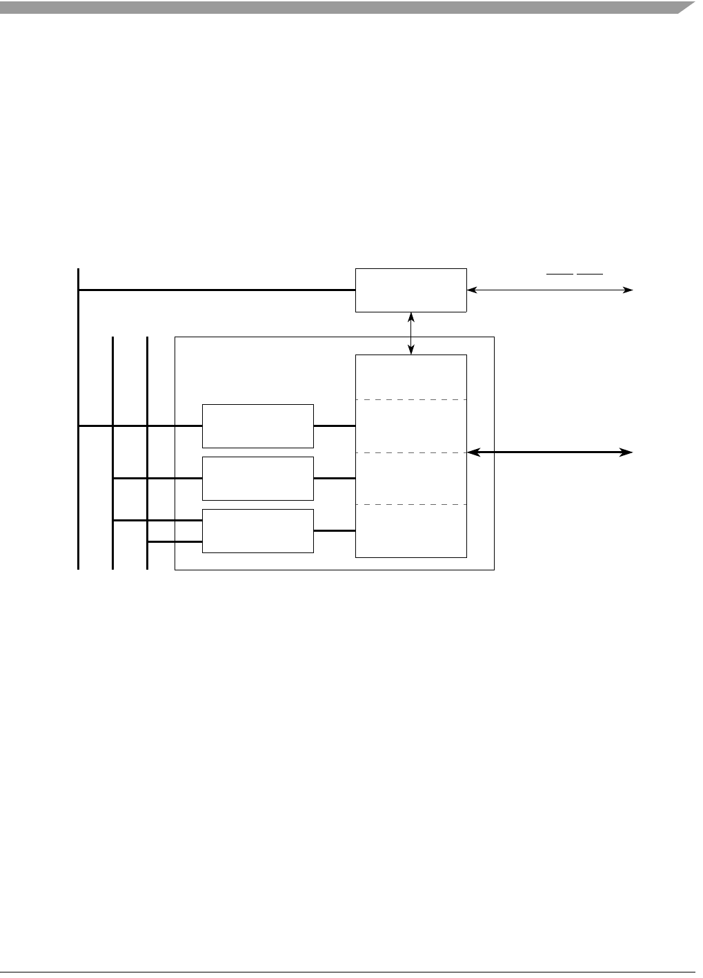
MCF548x Reference Manual, Rev. 3
Freescale Semiconductor 19-1
Chapter 19
PCI Bus Controller
19.1 Introduction
This chapter details the operation of the PCI bus controller for the MCF548x device. The PCI Bus Arbiter
is detailed in Chapter 20, “PCI Bus Arbiter Module.”
19.1.1 Block Diagram
Figure 19-1. PCI Block Diagram
19.1.2 Overview
The peripheral component interface (PCI) bus is a high-performance bus with multiplexed address and
data lines. It is especially suitable for high data-rate applications.
The PCI controller module supports a 32-bit PCI initiator (master) and target interface. As a target, access
to the internal XL bus is supported. As an initiator, the PCI controller is coupled directly to the XL bus (as
a slave) and available on the communication subsystem as a multichannel DMA peripheral.
The MCF548x contains PCI central resource functions such as the PCI Arbiter (Chapter 20, “PCI Bus
Arbiter Module”) and PCI reset control. The PCI bus clock must be provided by an external source. It must
be phase aligned and either equal to 1, 1/2, or 1/4 the frequency of the system clock.
19.1.3 Features
The following PCI features are supported in the MCF548x:
• Supports system clock: PCI clock frequency ratios 1:1, 2:1, and 4:1
• Uses external CLKIN as clock reference
PCI
Controller
Configuration
Interface
Targe t
Interface
Initiator
Interface
External PCI Bus
Req/Gnt
External REQ/GNT
Master Bus
Target
Configuration
PCI
Arbiter
Comm Bus
XL Bus
Slave Bus (IP Bus)
Master Bus/
Comm Bus Initiator
PCI Controller Block

MCF548x Reference Manual, Rev. 3
19-2 Freescale Semiconductor
• Compatible with PCI 2.2 specification
• PCI initiator and target operation
• Fully synchronous design
• 32-bit PCI address bus
• PCI 2.2 Type 0 configuration space header
• Supports the PCI 16/8 clock rule
• PCI master multichannel DMA or CPU access to PCI bus
• Ideal transfer rates up to 266 Mbytes/sec. (66 MHz clock, 128 byte buffer)
• PCI to system bus address translation
• Target response is medium DEVSEL generation
• Initiator latency time-outs
• Automatic retry of target disconnects
19.2 External Signal Description
For detailed description of the PCI bus signals, see the PCI Local Bus Specification, Revision 2.2.
19.2.1 Address/Data Bus (PCIAD[31:0])
The PCIAD[31:0] lines are a time multiplexed address data bus. The address is presented on the bus during
the address phase while the data is presented on the bus during one or more data phases.
19.2.2 Command/Byte Enables (PCICXBE[3:0])
The PCICXBE[3:0] lines are time multiplexed. The PCI command is presented during the address phase
and the byte enables are presented during the data phase. Byte enables are active low.
Table 19-1. PCI Module External Signals
Name Type Function MCF548x Reset
PCIAD[31:0] I/O PCI Address Data Bus Tristate
PCICXBE[3:0] I/O PCI Command/Bytes Enables Tristate
PCIDEVSEL I/O PCI Device Select Tristate
PCIFRAME I/O PCI Frame Tristate
PCIIDSEL IPCI Initialization Device Select Tristate
PCIIRDY I/O PCI Initiator Ready Tristate
PCIPAR I/O PCI Parity Tristate
CLKIN IPCI Clock Toggling
PCIPERR I/O PCI Parity Error Tristate
PCIRESET OPCI Reset 0
PCISERR I/O PCI System Error Tristate
PCISTOP I/O PCI Stop Tristate
PCITRDY I/O PCI Target Ready Tristate

External Signal Description
MCF548x Reference Manual, Rev. 3
Freescale Semiconductor 19-3
19.2.3 Device Select (PCIDEVSEL)
The PCIDEVSEL signal is asserted active low when the PCI controller decodes that it is the target of a
PCI transaction from the address presented on the PCI bus during the address phase.
19.2.4 Frame (PCIFRAME)
The PCIFRAME signal is asserted active low by a PCI initiator to indicate the beginning of a transaction.
It is deasserted when the initiator is ready to complete the final data phase.
19.2.5 Initialization Device Select (PCIIDSEL)
The PCIIDSEL signal is asserted active high during a PCI Type 0 Configuration Cycle to address the PCI
Configuration header.
19.2.6 Initiator Ready (PCIIRDY)
The PCIIRDY signal is asserted active low to indicate that the PCI initiator is ready to transfer data. During
a write operation, assertion indicates that the master is driving valid data on the bus. During a read
operation, assertion indicates that the master is ready to accept data.
19.2.7 Parity (PCIPAR)
The PCIPAR signal indicates the parity on the PCIAD[31:0] and PCICXBE[3:0] lines.
19.2.8 PCI Clock (CLKIN)
The CLKIN signal serves as a reference clock for generation of the internal PCI clock. For more
information, see Section 19.4.7, “PCI Clock Scheme.”
19.2.9 Parity Error (PCIPERR)
The PCIPERR signal is asserted active low when a data phase parity error is detected if enabled.
19.2.10 Reset (PCIRESET)
The PCIRESET signal is asserted active low by the PCI controller to reset the PCI bus. This signal is
asserted after MCF548x reset and must be negated to enable usage of the PCI bus.
19.2.11 System Error (PCISERR)
The PCISERR signal, if enabled, is asserted active low when an address phase parity error is detected.
19.2.12 Stop (PCISTOP)
The PCISTOP signal is asserted active low by the currently addressed target to indicate that it wishes to
stop the current transaction.

MCF548x Reference Manual, Rev. 3
19-4 Freescale Semiconductor
19.2.13 Target Ready (PCITRDY)
The PCITRDY signal is asserted active low by the currently addressed target to indicate that it is ready to
complete the current data phase.
19.3 Memory Map/Register Definition
The MCF548x has several sets of registers that control and report status for the different interfaces to the
PCI controller: PCI Type 0 configuration space registers, general status/control registers, and
communication subsystem interface registers. All of these registers are accessible as offsets of MBAR. As
an XL bus master, an external PCI bus master can access MBAR space for register updates.
PCIRESET is controlled by a bit in the register space, PCIGSCR[PR], and must first be cleared before
external PCI devices wake-up. In other words, an external PCI master cannot load configuration software
across the PCI bus until this bit is cleared by software. Access to all internal registers is supported
regardless of the value held in PCIGSCR[PR].
All registers are accessible at an offset of MBAR in the memory space. There are two module offsets for
PCI configuration space. One is allocated to the communication subsystem interface registers and the other
to all other PCI controller registers including the standard Type 0 PCI configuration space. Software reads
from unimplemented registers return 0x00000000 and writes have no effect.
Table 19-2. PCI Memory Map
Address Name Size Description Access
PCI Type 0 Configuration Registers
MBAR + 0xB00 PCIIDR 32 PCI Device ID/Vendor ID R
MBAR + 0xB04 PCISCR 32 PCI Status/Command R/W
MBAR + 0xB08 PCICCRIR 32 PCI Class Code/Revision ID R
MBAR + 0xB0C PCICR1 32 PCI Configuration 1 Register R/W
MBAR + 0xB10 PCIBAR0 32 PCI Base Address Register 0 R/W
MBAR + 0xB14 PCIBAR1 32 PCI Base Address Register 1 R/W
MBAR + 0xB18–0xB24 — — Reserved —
MBAR + 0xB28 PCICCPR 32 PCI Cardbus CIS Pointer R/W
MBAR + 0xB2C PCISID 32 Subsystem ID/Subsystem Vendor ID R/W
MBAR + 0xB30 PCIERBAR 32 PCI Expansion ROM R/W
MBAR + 0xB34 PCICPR 32 PCI Capabilities Pointer R/W
MBAR + 0xB38 — — Reserved —
MBAR + 0xB3C PCICR2 32 PCI Configuration Register 2 R/W
MBAR + 0xB40–0xB5C — — Reserved —
General Control/Status Registers
MBAR + 0xB60 PCIGSCR 32 Global Status/Control Register R/W
MBAR + 0xB64 PCITBATR0 32 Target Base Address Translation Register
0
R/W

Memory Map/Register Definition
MCF548x Reference Manual, Rev. 3
Freescale Semiconductor 19-5
MBAR + 0xB68 PCITBATR1 32 Target Base Address Translation Register
1
R/W
MBAR + 0xB6C PCITCR 32 Target Control Register R/W
MBAR + 0xB70 PCIIW0BTAR 32 Initiator Window 0 Base/Translation
Address Register
R/W
MBAR + 0xB74 PCIIW1BTAR 32 Initiator Window 1 Base/Translation
Address Register
R/W
MBAR + 0xB78 PCIIW2BTAR 32 Initiator Window 2 Base/Translation
Address Register
R/W
MBAR + 0xB7C — — Reserved —
MBAR + 0xB80 PCIIWCR 32 Initiator Window Configuration Register R/W
MBAR + 0xB84 PCIICR 32 Initiator Control Register R/W
MBAR + 0xB88 PCIISR 32 Initiator Status Register R/W
MBAR + 0xB8C–0xBF4 — — Reserved —
MBAR + 0xBF8 PCICAR 32 Configuration Address Register R/W
MBAR + 0xBFC — — Reserved —
CommBus FIFO Transmit Interface Registers1
MBAR + 0x8400 PCITPSR 32 Tx Packet Size Register R/W
MBAR + 0x8404 PCITSAR 32 Tx Start Address Register R/W
MBAR + 0x8408 PCITTCR 32 Tx Transaction Control Register R/W
MBAR + 0x840C PCITER 32 Tx Enables Register R/W
MBAR + 0x8410 PCITNAR 32 Tx Next Address Register R
MBAR + 0x8414 PCITLWR 32 Tx Last Word Register R
MBAR + 0x8418 PCITDCR 32 Tx Done Counts Register R
MBAR + 0x841C PCITSR 32 Tx Status Register R/WC
MBAR + 0x8420–0x843C — — Reserved —
MBAR + 0x8440 PCITFDR 32 Tx FIFO Data Register R/W
MBAR + 0x8444 PCITFSR 32 Tx FIFO Status Register R/WC
MBAR + 0x8448 PCITFCR 32 Tx FIFO Control Register R/W
MBAR + 0x844C PCITFAR 32 Tx FIFO Alarm Register R/W
MBAR + 0x8450 PCITFRPR 32 Tx FIFO Read Pointer Register R/W
MBAR + 0x8454 PCITFWPR 32 Tx FIFO Write Pointer Register R/W
MBAR + 0x8458–0x847C — — Reserved —
Table 19-2. PCI Memory Map (Continued)
Address Name Size Description Access

MCF548x Reference Manual, Rev. 3
19-6 Freescale Semiconductor
19.3.1 PCI Type 0 Configuration Registers
The PCI controller supplies a type 0 PCI configuration space header. These registers are accessible as an
offset from MBAR or through externally mastered PCI configuration cycles. PCI Dword Reserved space
(0x10–0x3F) can be accessed only from external PCI configuration accesses.
CommBus FIFO Receive Interface Registers1
MBAR + 0x8480 PCIRPSR 32 Rx Packet Size Register R/W
MBAR + 0x8484 PCIRSAR 32 Rx Start Address Register R/W
MBAR + 0x8488 PCIRTCR 32 Rx Transaction Control Register R/W
MBAR + 0x848C PCIRER 32 Rx Enables Register R/W
MBAR + 0x8490 PCIRNAR 32 Rx Next Address Register R
MBAR + 0x8494 — — Reserved —
MBAR + 0x8498 PCIRDCR 32 Rx Done Counts Register R
MBAR + 0x849C PCIRSR 32 Rx Status Register R/WC
MBAR + 0x84A0–0x84BC — — Reserved —
MBAR + 0x84C0 PCIRFDR 32 Rx FIFO Data Register R/W
MBAR + 0x84C4 PCIRFSR 32 Rx FIFO Status Register R/WC
MBAR + 0x84C8 PCIRFCR 32 Rx FIFO Control Register R/W
MBAR + 0x84CC PCIRFAR 32 Rx FIFO Alarm Register R/W
MBAR + 0x84D0 PCIRFRPR 32 Rx FIFO Read Pointer Register R/W
MBAR + 0x84D4 PCIRFWPR 32 Rx FIFO Write Pointer Register R/W
MBAR + 0x84D8–0x84FC — — Reserved —
1The PCI controller has separate control registers for transmit and receive operations via the communication subsystem
DMA. See Section 19.3.3, “Communication Subsystem Interface Registers” for more information on these registers.
Table 19-2. PCI Memory Map (Continued)
Address Name Size Description Access

Memory Map/Register Definition
MCF548x Reference Manual, Rev. 3
Freescale Semiconductor 19-7
19.3.1.1 Device ID/Vendor ID Register (PCIIDR)—PCI Dword Addr 0
19.3.1.2 PCI Status/Command Register (PCISCR)—PCI Dword Addr 1
31 30 29 28 27 26 25 24 23 22 21 20 19 18 17 16
RDevice ID
W
Reset0101100000000110
1514131211109876543210
R Vendor ID
W
Reset0001000001010111
Reg
Addr
MBAR + 0xB00
Figure 19-2. Device ID/Vendor ID Register (PCIIDR)
Table 19-3. PCIIDR Field Descriptions
Bits Name Description
31–16 Device ID This field is read-only and represents the PCI Device Id assigned to the MCF548x. Its
value is: 0x5806.
15–0 Vendor ID This field is read-only and represents the PCI Vendor Id assigned to the MCF548x. Its
value is: 0x1057.
31 30 29 28 27 26 25 24 23 22 21 20 19 18 17 16
RPESEMATRTS DT DPFC R66MC 0 0 0 0
Wrwc
1rwc1rwc1rwc1rwc1rwc1
Reset0000001010100000
15 14 13 12 11 10 9 8 7 6 5 4 3 2 1 0
R000000F S ST PER VMW SP BMIO
W
Reset0000000000000000
Reg
Addr
MBAR + 0xB04
1Bits 31-27 and 24 are read-write-clear (rwc).
—Hardware can set rwc bits, but cannot clear them.
—Only PCI configuration cycles can clear rwc bits that are currently set by writing a 1 to the bit location.
Writing a 1 to a rwc bit that is currently a 0 or writing a 0 to any rwc bit has no effect.
Figure 19-3. PCI Status/Command Register (PCISCR)

MCF548x Reference Manual, Rev. 3
19-8 Freescale Semiconductor
Table 19-4. PCISCR Field Descriptions
Bits Name Description
31 PE Parity error detected. This bit is set when a parity error is detected, even if the PCISCR[PER] is cleared.
This bit is cleared by a PCI configuration cycle writing a ‘1’ to the bit. Writing ‘0’ has no effect.
30 SE System error signalled. This bit is set whenever the PCI controller generates a PCI system error on the
PCISERR line. This bit is cleared by a PCI configuration cycle writing a ‘1’ to the bit. Writing ‘0’ has no
effect.
29 MA Master abort received. This bit is set whenever the PCI controller is the PCI master and terminates a
transaction (except for a special cycle) with a master-abort. This bit is cleared by a PCI configuration
cycle writing a ‘1’ to the bit. Writing ‘0’ has no effect.
28 TR Target abort received. This bit is set whenever the PCI controller is the PCI master and a transaction
is terminated by a target-abort from the currently addressed target. This bit is cleared by a PCI
configuration cycle writing a ‘1’ to the bit. Writing ‘0’ has no effect.
27 TS Target abort signalled. This bit is set whenever the PCI controller is the target and it terminates a
transaction with a target-abort. This bit is cleared by a PCI configuration cycle writing a ‘1’ to the bit.
Writing ‘0’ has no effect.
26–25 DT DEVSEL timing. Fixed to ‘01’. These bits encode a medium DEVSEL timing. This defines the slowest
DEVSEL timing as meduim timing when the PCI controller is the target (except configuration
accesses).
24 DP Master data parity error. This bit applies only when the PCI controller is the master and is set only if the
following conditions are met:
• The PCI controller-as-master sets PERR itself during a read or the PCI controller-as-master
detected it asserted by the target during a write
• The PCISCR[PER] bit is set
This bit is cleared by a PCI configuration cycle writing a ‘1’ to the bit. Writing ‘0’ has no effect.
23 FC Fast back-to-back capable. Fixed to 1. This read-only bit indicates that the PCI controller as target is
capable of accepting fast back-to-back transactions with other targets.
22 R Reserved. Fixed to 0. Prior to the 2.2 PCI Spec, this was the UDF (user defined features) supported bit.
0 Does not support UDF
1 Supported user defined features
21 66M 66 MHz capable. Fixed to 1. This bit indicates that the PCI controller is 66 MHz capable.
20 C Capabilities list. Fixed to 0. This bit indicates that the PCI controller does not implement the New
Capabilities List Pointer Configuration Register in DWORD 13 of the configuration space.
19–10 — Reserved, should be cleared.
9 F Fast back-to-back transfer enable. This bit controls whether or not the PCI controller as master can do
fast back-to-back transactions to different devices. Initialization software should set this bit if all targets
are fast back-to-back capable.
0 Fast back-to-back transactions are only allowed to the same device
1 The master is allowed to generate fast back-to-back transactions to different devices.
8 S SERR enable. This bit is an enable bit for the PCISERR driver.
0 PCISERR driver disabled
1 PCISERR driver enabled
Note: Address parity errors are reported only if this bit and bit 6 are set.
7 ST Address and data stepping. Fixed to 0. This bit indicates that the PCI controller never uses
address/data stepping. Initialization software should write a 0 to this bit location.

Memory Map/Register Definition
MCF548x Reference Manual, Rev. 3
Freescale Semiconductor 19-9
19.3.1.3 Revision ID/Class Code Register (PCICCRIR)—PCI Dword 3
6 PER Parity error response. This bit controls the device’s response to parity errors.
0 The device sets its Parity Error status bit (bit 31) in the event of a parity error, but does not assert
PERR.
1 When a parity error is detected, the PCI controller asserts PERR
5 V VGA palette snoop enable. Fixed to 0. This bit indicates that the PCI controller is not VGA compatible.
Initialization software should write a 0 to this bit location.
4 MW Memory write and invalidate enable. This bit is an enable for using the memory write and invalidate
command.
0 Only memory write command can be used
1 PCI controller-as-master may generate the memory write and invalidate command.
3 SP Special cycle monitor or ignore. This bit is to determine whether or not to ignore PCI Special Cycles.
Since PCI controller-as-target does not recognize messages delivered via the Special Cycle operation,
a value of 1 should never be programmed to this register. This bit, however, is programmable
(read/write from both the IP bus and PCI bus Configuration cycles).
2 B Bus master enable. This bit indicates whether or not the PCI controller has the ability to serve as a
master on the PCI bus. A value of 1 indicates this ability is enabled. If the PCI controller is used as a
master on the PCI bus (via the XL bus or comm bus), a 1 should be written to this bit during initialization.
If the value of the register is 0, it will not inhibit mastered transactions. This bit is meant to be read by
configuration software.
1 M Memory access control. This bit controls the PCI controller’s response to memory space accesses.
0 The PCI controller does not recognize memory accesses
1 The PCI controller recognizes memory accesses.
0 IO I/O access control. Fixed to 0. This bit is not implemented because there is no PCI controller I/O type
space accessible from the PCI bus. The PCI base address registers are memory address ranges only.
Initialization software should write a 0 to this bit location.
31 30 29 28 27 26 25 24 23 22 21 20 19 18 17 16
R Class Code
W
Reset0000011010000000
1514131211109876543210
R Class Code Revision ID
W
Reset0000000000000000
Reg
Addr
MBAR + 0xB08
Figure 19-4. Revision ID/Class Code Register (PCICCRIR)
Table 19-4. PCISCR Field Descriptions (Continued)
Bits Name Description

MCF548x Reference Manual, Rev. 3
19-10 Freescale Semiconductor
19.3.1.4 Configuration 1 Register (PCICR1)—PCI Dword 3
Table 19-5. PCICCRIR Field Descriptions
Bits Name Description
31–8 Class Code This field is read-only and represents the PCI Class Code assigned to processor. Its value
is: 0x06 8000. (Other bridge device).
7–0 Revision ID This field is read-only and represents the PCI Revision ID for this version of the processor.
Its value is: 0x00.
31 30 29 28 27 26 25 24 23 22 21 20 19 18 17 16
RBIST Header Type
W
Reset0000000000000000
1514131211109876543210
R Lat Timer [7:3] Lat Timer [2:0] Cache Line Size [7:4] Cache Line Size [3:0]
W
Reset0000000000000000
Reg
Addr
MBAR + 0xB0C
Figure 19-5. Configuration 1 Register (PCICR1)
Table 19-6. PCICR1 Field Descriptions
Bits Name Description
31–24 BIST Built in self test. Fixed to 0x00. The PCI controller does not implement the Built-In Self Test
register. Initialization software should write a 0x00 to this register location.
23–16 Header
Type
Header type. Fixed to 0x00. The PCI controller implements a Type 0 PCI configuration
space Header. Initialization software should write a 0x00 to this register location.
15–11 Lat Timer Latency timer [7:3]. This register contains the latency timer value, in PCI clocks, used when
the PCI controller is the PCI master. The upper five bits are programmable.
Latency timer must be programmed to a non-zero value before the PCI Controller will
operate as master of the PCI bus.
10-8 Latency timer [2:0] The lower three bits of the register are hardwired low
7–4 Cache Line
Size
Cache line size[7:4] Specifies the cache line size in units of DWORDs. The higher four bits
of the register are hardwired low
3–0 Cache line size [3:0] Specifies the cache line size in units of DWORDs.

Memory Map/Register Definition
MCF548x Reference Manual, Rev. 3
Freescale Semiconductor 19-11
19.3.1.5 Base Address Register 0 (PCIBAR0)—PCI Dword 4
31 30 29 28 27 26 25 24 23 22 21 20 19 18 17 16
RBAR 0 0 0
W
Reset0000000000000000
1514131211109876543210
R000000000000PREFRANGEIO/M#
W
Reset0000000000000000
Reg
Addr
MBAR + 0xB10
Figure 19-6. Base Address Register 0 (PCIBAR0)
Table 19-7. PCIBAR0 Field Descriptions
Bits Name Description
31–18 BAR0 Base address register 0. PCI base address register 0 (256 Kbyte). Applies only when
processor is target. These bits are programmable (read/write from both the IP bus and PCI
bus Configuration cycles).
17–4 — Reserved, should be cleared.
3 PREF Prefetchable access. Fixed to 0. This bit indicates that the memory space defined by BAR0
is not prefetchable. Configuration software should write a 0 to this bit location.
2–1 RANGE Fixed to 00. This register indicates that base address 0 is 32 bits wide and can be mapped
anywhere in 32-bit address space. Configuration software should write 00 to these bit
locations.
0 IO/M# IO or memory space. Fixed to 0. This bit indicates that BAR0 is for memory space.
Configuration software should write a 0 to this bit location.
0 Memory
1I/O

MCF548x Reference Manual, Rev. 3
19-12 Freescale Semiconductor
19.3.1.6 Base Address Register 1 (PCIBAR1)—PCI Dword 5
19.3.1.7 CardBus CIS Pointer Register PCICCPR—PCI Dword A
This optional register contains the pointer to the Card Information Structure (CIS) for the CardBus card.
All 32 bits of the register are programmable by the slave bus. From the PCI bus, this register can only be
read, not written. Its reset value is 0x0000 0000 and is accessible at address MBAR + 0xB28.
19.3.1.8 Subsystem ID/Subsystem Vendor ID Registers PCISID—PCI Dword B
The Subsystem Vendor ID register contains the 16-bit manufacturer identification number of the add-in
board or subsystem that contains this PCI device. The Subsystem ID register contains the 16-bit subsystem
identification number of the add-in board or subsystem that contains this PCI device. A value of zero in
these registers indicates there isn’t a Subsystem Vendor and Subsystem ID associated with the device. If
used, software must write to these registers before any PCI bus master reads them.
31 30 29 28 27 26 25 24 23 22 21 20 19 18 17 16
RBAR1 00000000000000
W
Reset0000000000000000
1514131211109876543210
R000000000000PREFRANGEIO/M#
W
Reset0000000000001000
Reg
Addr
MBAR + 0xB14
Figure 19-7. Base Address Register 1 (PCIBAR1)
Table 19-8. PCIBAR1 Field Descriptions
Bits Name Description
31–30 BAR1 Base address register 1. Processo PCI base address register 1 (1 Gbyte). Applies only
when the processor is target. These bits are programmable (read/write from both the IP
bus and PCI bus Configuration cycles).
29–4 — Reserved, should be cleared.
3 PREF Prefetchable access. Fixed to 1. This bit indicates that the memory space defined by BAR1
is prefetchable. Configuration software should write a 1 to this bit location.
2–1 RANGE Fixed to 00. This register indicates that base address 1 is 32 bits wide and can be mapped
anywhere in 32-bit address space. Configuration software should write 00 to these bit
locations.
0 IO/M# IO or memory space. Fixed to 0. This bit indicates that BAR1 is for memory space.
Configuration software should write a 0 to this bit location.
0 Memory
1I/O

Memory Map/Register Definition
MCF548x Reference Manual, Rev. 3
Freescale Semiconductor 19-13
All 32 bits of the register are programmable by the slave bus. From the PCI bus, this register can only be
read, not written. The reset value is 0x0000_0000 and is accessible at address MBAR + 0xB2C.
19.3.1.9 Expansion ROM Base Address PCIERBAR—PCI Dword C
Not implemented. Fixed to 0x0000_0000 at address MBAR + 0xB30.
19.3.1.10 Capabilities Pointer (Cap_Ptr) PCICPR—PCI Dword D
Not implemented. Fixed to 0x00 at address MBAR + 0xB34.
19.3.1.11 Configuration 2 Register (PCICR2)—PCI Dword F
19.3.2 General Control/Status Registers
The general control/status registers primarily address the configurability of the XL bus initiator and target
interfaces, though some also address global options which affect the multichannel DMA interface. These
31 30 29 28 27 26 25 24 23 22 21 20 19 18 17 16
RMax_Lat Min_Gnt
W
Reset0000000000000000
1514131211109876543210
R Interrupt Pin Interrupt Line
W
Reset0000000000000000
Reg
Addr
MBAR + 0xB3C
Figure 19-8. Configuration 2 Register (PCICR2)
Table 19-9. PCICR2 Field Descriptions
Bits Name Description
31–24 Max_Lat Maximum latency. Specifies how often, in units of 1/4 microseconds, the PCI controller would
like to have access to the PCI bus as master. A value of zero indicates the device has no
stringent requirement in this area. The register is read/write to/from the slave bus, but read only
from the PCI bus.
23–16 Min_Gnt Minimum grant. The value programmed to this register indicates how long the PCI controller as
master would like to retain PCI bus ownership whenever it initiates a transaction. The register is
programmable from the slave bus, but read only from the PCI bus.
15–8 Interrupt
Pin
Fixed to 0x00. Indicates that this device does not use an interrupt request pin.
7–0 Interrupt
Line
Fixed to 0x00. The Interrupt Line register stores a value that identifies which input on a PCI
interrupt controller the function’s PCI interrupt request pin. Since no interrupt request pin is used,
as specified in the Interrupt Pin register, this register has no function.
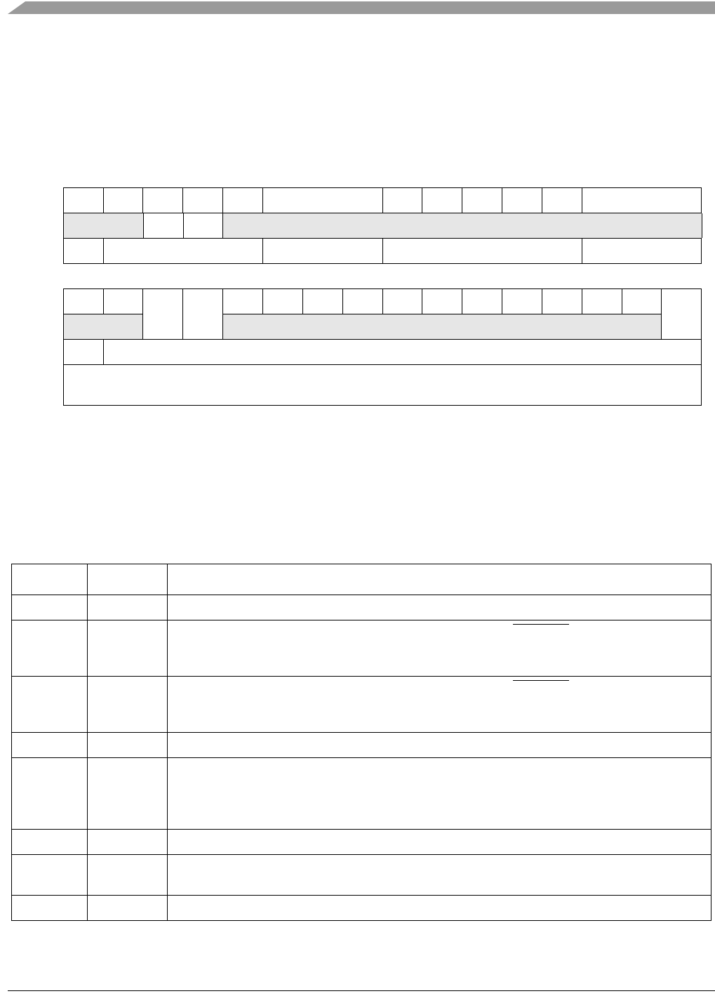
MCF548x Reference Manual, Rev. 3
19-14 Freescale Semiconductor
registers are accessed primarily internally as offsets of MBAR, but can also be accessed by an external PCI
master if PCI base and target base address registers are configured to access the space. See Section 19.5.2,
“Address Maps,” on configuring address windows.
19.3.2.1 Global Status/Control Register (PCIGSCR)
31 30 29 28 27 26 25 24 23 22 21 20 19 18 17 16
R0 0PE SE 0 XLB2CLKIN 0 0000 Reserved
Wrwc1rwc1
Reset00000 —
20 0 0 0 0 Uninitialized
1514131211109876543210
R0 0PEE SEE 0 0000000000PR
W
Reset0000000000000001
Reg
Addr
MBAR + 0xB60
1Bits 29 and 28 are read-write-clear (rwc).
—Hardware can set rwc bits, but cannot clear them.
—Software can clear rwc bits that are currently set by writing a 1 to the bit location. Writing a 1 to a rwc bit that is
currently a 0 or writing a 0 to any rwc bit has no effect.
2The reset value of bits 26-24 and 18-16 is determined by the PLL multiplier.
Figure 19-9. Global Status/Control Register (PCIGSCR)
Table 19-10. PCIGSCR Field Descriptions
Bits Name Description
31–30 — Reserved, should be cleared.
29 PE PERR detected. This bit is set when the PCI Parity Error line, PCIPERR, asserts (any device). A
CPU interrupt will be generated if the PCIGSCR[PEE] bit is set. It is up to application software to
clear this bit by writing ‘1’ to it.
28 SE SERR detected. This bit is set when a PCI System Error line, PCISERR, asserts (any device). A
CPU interrupt will be generated if the PCIGSCR[SEE] bit is set. It is up to application software to
clear this bit by writing ‘1’ to it.
27 — Reserved, should be cleared.
26–24 XLB2CLKIN This bit field stores the XL bus clock to external PCI clock (CLKIN)divide ratio. This field is
read-only and the reset value is determined by the PLL multiplier (either 1, 2, or 4). Software can
read these bits to determine a valid ratio. If the register contains a differential value that does not
reflect the PLL settings, the PCI controller could malfunction.
23–19 — Reserved, should be cleared.
18–16 CLKINReser
ved
This field is reserved.
15–14 — Reserved, should be cleared.

Memory Map/Register Definition
MCF548x Reference Manual, Rev. 3
Freescale Semiconductor 19-15
19.3.2.2 Target Base Address Translation Register 0 (PCITBATR0)
13 PEE Parity error interrupt enable. This bit enables CPU Interrupt generation when the PCI Parity Error
signal, PCIPERR, is sampled asserted. When enabled and PCIPERR asserts, software must
clear the PE status bit to clear the interrupt condition.
12 SEE System error interrupt enable. This bit enables CPU Interrupt generation when a PCI system error
is detected on the PCISERR line. When enabled and PCISERR asserts, software must clear the
SE status bit to clear the interrupt condition.
11–1 — Reserved, should be cleared.
0 PR PCI reset. This bit controls the external PCIRESET. When this bit is cleared, the external
PCIRESET deasserts. Setting this bit does not reset the internal PCI controller. The application
software must not initiate PCI transactions while this bit is set. It is recommended that this bit be
programmed last during initialization.
The reset value of the bit is 1 (PCIRESET asserted).
31 30 29 28 27 26 25 24 23 22 21 20 19 18 17 16
RBase Address Translation 0 0 0
W
Reset0000000000000000
1514131211109876543210
R000000000000000EN
W
Reset0000000000000000
Reg
Addr
MBAR + 0xB64
Figure 19-10. Target Base Address Translation Register 0 (PCITBATR0)
Table 19-11. PCITBATR0 Field Descriptions
Bits Name Description
31–18 Base
Address
Translation 0
This base address register corresponds to a hit on the BAR0 in MCF548x PCI Type 0 Configuration
space register from PCI space. When there is a hit on MCF548x PCI BAR0 (MCF548x as Target),
the upper 14 bits of the address (256-Kbyte boundary) are written over by this register value to
address some space in MCF548x. In normal operation, this value should be written during the
initialization sequence only.
17–1 — Reserved, should be cleared.
0 Enable 0 This bit enables a transaction in BAR0 space. If this bit is zero and a hit on MCF548 PCIBAR0
occurs, the target interface gasket will abort the PCI transaction.
Table 19-10. PCIGSCR Field Descriptions (Continued)
Bits Name Description

MCF548x Reference Manual, Rev. 3
19-16 Freescale Semiconductor
19.3.2.3 Target Base Address Translation Register 1 (PCITBATR1)
19.3.2.4 Target Control Register (PCITCR)
31 30 29 28 27 26 25 24 23 22 21 20 19 18 17 16
RBase Address
Translation 1
00000000000000
W
Reset0000000000000000
1514131211109876543210
R000000000000000EN
W
Reset0000000000000000
Reg
Addr
MBAR + 0xB68
Figure 19-11. Target Base Address Translation Register 1 (PCITBATR1)
Table 19-12. PCITBATR1 Field Descriptions
Bits Name Description
31–30 Base
Address
Translation
1
This base address register corresponds to a hit on the BAR1 in MCF548 PCI Type 0 Configuration
space register (PCI space). When there is a hit on MCF548 PCI BAR1 (MCF548 as Target), the
upper 2 bits of the address (1-Gbyte boundary) are written over by this register value to address
some 1-Gbyte space in MCF548. This register can be reprogrammed to move the window of
MCF548 address space accessed during a hit in PCIBAR1.
29–1 — Reserved, should be cleared.
0 EN This bit enables a transaction in BAR1 space. If this bit is zero and a hit on MCF548 PCI BAR1
occurs, the target interface gasket will abort the PCI transaction.
31 30 29 28 27 26 25 24 23 22 21 20 19 18 17 16
R0000000LD0000 0 0 0 P
W
Reset0000000000000000
1514131211109876543210
R0000000000000000
W
Reset0000000000000000
Reg
Addr
MBAR + 0xB6C
Figure 19-12. Target Control Register (PCITCR)

Memory Map/Register Definition
MCF548x Reference Manual, Rev. 3
Freescale Semiconductor 19-17
19.3.2.5 Initiator Window 0 Base/Translation Address Register (PCIIW0BTAR)
Table 19-13. PCITCR Field Descriptions
Bits Name Description
31–25 — Reserved, should be cleared.
24 LD Latency rule disable. This control bit applies only when MCF548 is Target. When set, it prevents the
PCI Controller from automatically issuing a retry disconnect due to the PCI 16/8 clock rule.
This bit should only be set when the XL<->PCI path is not in use. The only transactions that are retried
on the XL bus by the PCI are reads. Writes are held on the XL bus until either all data is posted (PCI
memory writes) and the XL bus data tenure is normally terminated or, in the case of I/O writes to PCI,
access is granted to the PCI bus and the connected write completes. When the LD bit is set, there is
never a timeout on the PCI bus because the PCI 16/8 clock rule is not obeyed. If there is inbound PCI
traffic (PCI->MCF548) and an XL bus write is held open by the PCI Controller, the PCI traffic will not
be granted access to XL bus. This is true for reads that have not been prefetched and when the
inbound write buffer is full. Both buses hang. Normal operation relies on the LD bit being cleared.
If used, the bit must be set before the 15th PCI clock for the first transfer and before the 7th clock for
other transfers.
23–17 — Reserved, should be cleared.
16 P Prefetch reads. This bit controls fetching a line from memory in anticipation of a request from the
external master. The target interface will continue to prefetch lines from memory as long as
PCIFRAME is asserted and there is space to store the data in the target read buffer.
Note: This bit only applies to PCI reads in the address range for BAR 1 (prefetchable memory).
Note: Prefetching is performed in response to a PCI memory-read-multiple command even if this bit
is cleared.
15–0 — Reserved, should be cleared.
31 30 29 28 27 26 25 24 23 22 21 20 19 18 17 16
R Window 0 Base Address Window 0 Address Mask
W
Reset0000000000000000
1514131211109876543210
R Window 0 Translation Address 00000000
W
Reset0000000000000000
Reg
Addr
MBAR + 0xB70
Figure 19-13. Initiator Window 0 Base/Translation Address Register (PCIIW0BTAR)

MCF548x Reference Manual, Rev. 3
19-18 Freescale Semiconductor
19.3.2.6 Initiator Window 1 Base/Translation Address Register (PCIIW1BTAR)
The field descriptions for this register are the same as for PCIIW0BTAR, except that they apply to Window
1.
Table 19-14. PCIIW0BTAR Field Descriptions
Bits Name Description
31–24 Window 0
Base
Address
One of three base address registers to determine an XL bus hit on PCI. At most, the upper byte of
the address is decoded. The Window 0 Address Mask register determines what bits of this register
to compare the XL bus address against to generate the hit.
The smallest possible Window is a 16-Mbyte block.
23–16 Window 0
Address
Mask
The Window 0 Address Mask Register masks the corresponding XL bus base address bit of the
base address for Window 0 (Window 0 Base Address) to instruct the address decode logic to
ignore or “don’t care” the bit. If the base address mask bit is set, the associated base address bit
of Window 0 is ignored when generating the PCI hit. Bit 16 masks bit 24, bit 17 masks bit 25, and
so on.
0 Corresponding address bit is used in address decode.
1 Corresponding address bit is ignored in address decode.
For XL bus accesses to Window 0 address range, this byte also determines which upper 8 bits of
the XL bus address to pass on for presentation as a PCI address. Any address bit used to decode
the XL bus address, indicated by a “0”, will be translated. This provides a way to overlay a PCI page
address onto the XL bus address. A “1” in the Address Mask byte indicates that the XL bus address
bit will be passed to PCI unaltered.
15–8 Window 0
Translation
Address
For any translated bit (described above), the corresponding value here will be driven onto the PCI
address bus for the XL bus Window 0 address hit.
The Window Translation operation can not be turned off. If a direct mapping from XL bus to PCI
space is desired, program the same value to both the Window Base Address Register and Window
Translation Address Register.
7–0 — Reserved, should be cleared.
31 30 29 28 27 26 25 24 23 22 21 20 19 18 17 16
R Window 1 Base Address Window 1 Address Mask
W
Reset0000000000000000
1514131211109876543210
R Window 1 Translation Address 00000000
W
Reset0000000000000000
Reg
Addr
MBAR + 0xB74
Figure 19-14. Initiator Window 1 Base/Translation Address Register (PCIIW1BTAR)

Memory Map/Register Definition
MCF548x Reference Manual, Rev. 3
Freescale Semiconductor 19-19
19.3.2.7 Initiator Window 2 Base/Translation Address Register (PCIIW2BTAR)
The field descriptions for this register are the same as for PCIIW0BTAR, except that they apply to Window
2.
19.3.2.8 Initiator Window Configuration Register (PCIIWCR)
31 30 29 28 27 26 25 24 23 22 21 20 19 18 17 16
R Window 2 Base Address Window 2 Address Mask
W
Reset0000000000000000
1514131211109876543210
R Window 2 Translation Address 00000000
W
Reset0000000000000000
Reg
Addr
MBAR + 0xB78
Figure 19-15. Initiator Window 2 Base/Translation Address Register (PCIIW2BTAR)
31 30 29 28 27 26 25 24 23 22 21 20 19 18 17 16
R0000 Window 0 Control 0000 Window 1 Control
W
Reset0000000000000000
1514131211109876543210
R0000 Window 2 Control 00000000
W
Reset0000000000000000
Reg
Addr
MBAR + 0xB80
Figure 19-16. Initiator Window Configuration Register (PCIIWCR)

MCF548x Reference Manual, Rev. 3
19-20 Freescale Semiconductor
19.3.2.9 Initiator Control Register (PCIICR)
Table 19-15. PCIIWCR Field Descriptions
Bits Name Description
31–28 — Reserved, should be cleared.
27–24 Window 0
Control[3:0]
Bit[3]—IO/M#.
0 Window is mapped to PCI memory.
1 Window is mapped to PCI I/O.
Bit[2:1]—PCI read command (PRC).
If bit[3] is programmed memory, “0”, then these bits are used to determine the type of PCI memory
command to issue. See Table 19-57. If bit[3] is set to “1”, the value of these bits is meaningless.
00 PCI Memory Read.
01 PCI Memory Read Line.
10 PCI Memory Read Multiple.
11 Reserved.
Bit[0]—Enable.
This bit is set to indicate the address registers that control the XL bus initiator interface access to
PCI initialized and will be used. The PCI Controller can begin to decode XL bus PCI accesses.
0 Do not decode XL bus PCI accesses to Window.
1 Registers initialized—decode accesses to Window.
23–20 — Reserved, should be cleared.
19–16 Window 1
Control[3:0]
Bit[3]—IO/M#.
Bit[2:1]—PRC.
Bit[0]—Enable.
15–12 Reserved Reserved register. Write a zero to this register.
11–8 Window 2
Control[3:0]
Bit[3]—IO/M#.
Bit[2:1]—PRC.
Bit[0]—Enable.
7–0 — Reserved, should be cleared.
31 30 29 28 27 26 25 24 23 22 21 20 19 18 17 16
R00000REEIAETAE00000000
W
Reset0000000000000000
1514131211109876543210
R00000000 Maximum Retries
W
Reset0000000011111111
Reg
Addr
MBAR + 0xB84
Figure 19-17. Initiator Control Register (PCIICR)

Memory Map/Register Definition
MCF548x Reference Manual, Rev. 3
Freescale Semiconductor 19-21
19.3.2.10 Initiator Status Register (PCIISR)
Table 19-16. PCIICR Field Descriptions
Bits Name Description
31–27 — Reserved, should be cleared.
26 REE Retry error enable. This bit enables CPU Interrupt generation in the case of Retry Error termination
of a transaction. It may be desirable to mask CPU interrupts, but in such a case, software should
poll the status bits to prevent a possible lock-up condition.
25 IAE Initiator abort enable. This bit enables CPU Interrupt generation in the case of Initiator Abort
termination of a transaction. It may be desirable to mask CPU interrupts, but in such a case,
software should poll the status bits to prevent a possible lock-up condition.
24 TAE Target abort enable. This bit enables CPU Interrupt generation in the case of Target Abort
termination of a transaction. It may be desirable to mask CPU interrupts, but in such a case,
software should poll the status bits to prevent a possible lock-up condition.
23–8 — Reserved, should be cleared.
7–0 Maximum
Retries
This bit field controls the maximum number of automatic PCI retries or master latency time-outs to
permit per write transaction. The retry counter is reset at the beginning of each write transaction
(i.e. it is not cumulative). Setting the Maximum Retries to 0x00 allows infinite automatic retry cycles
and latency time-outs before the write transaction will abort and, if open, send back an error on XL
bus. A slow or malfunctioning Target might issue infinite retry disconnects or hold the data tenure
open indefinitely, and therefore, permanently tie up the PCI bus if no Target Abort occurs.
The Maximum Retries register does not apply to reads because reads are always ARTRY’d on XL
bus when retry-terminated by the PCI target. This is done to avoid livelock scenarios where the
device we are requesting read data from needs to flush itself of posted writes going to MCF548
before it can return the read data. The incoming writes cannot be blocked in this case.
31 30 29 28 27 26 25 24 23 22 21 20 19 18 17 16
R00000REIATA00000000
Wrwc1rwc1rwc1
Reset0000000000000000
1514131211109876543210
R0000000000000000
W
Reset0000000000000000
Reg
Addr
MBAR + 0xB88
1Bits 26-24 are read-write-clear (rwc).
—Hardware can set rwc bits, but cannot clear them.
—Software can clear rwc bits that are currently set by writing a 1 to the bit location. Writing a 1 to a rwc bit that is
currently a 0 or writing a 0 to any rwc bit has no effect.
Figure 19-18. Initiator Status Register (PCIISR)

MCF548x Reference Manual, Rev. 3
19-22 Freescale Semiconductor
19.3.2.11 Configuration Address Register (PCICAR)
Table 19-17. PCIISR Field Descriptions
Bits Name Description
31–27 — Reserved, should be cleared.
26 RE Retry error. This flag is set when the controller ARTRY’s a read on XL bus when retry-terminated
by the PCI target or when the Max_Retries limit is reached for a single XL bus write transaction.
A CPU interrupt will be generated if PCIICR[RE] bit is set. It is up to application software to clear
this bit by writing ‘1’ to it.
25 IA Initiator abort. This flag bit is set if the PCI controller issues an Initiator Abort flag. This indicates
that no Target responded by asserting DEVSEL within the time allowed for subtractive decoding.
A CPU interrupt will be generated if the PCIICR[IAE] bit is set. It is up to application software to
clear this bit by writing ‘1’ to it.
24 TA Target abort. This flag bit is set if the addressed PCI Target has signalled an Abort. A CPU
interrupt will be generated if the PCIICR[TAE] bit is set. It is up to application software to query
the Target’s status register and determine the source of the error. It is up to application software
to clear this bit by writing ‘1’ to it.
23–0 — Reserved, should be cleared.
31 30 29 28 27 26 25 24 23 22 21 20 19 18 17 16
R E 0 0 0 0 0 0 0 Bus Number
W
Reset0000000000000000
1514131211109876543210
R Device Number Function Number DWORD 0 0
W
Reset0000000000000000
Reg
Addr
MBAR + 0xBF8
Figure 19-19. Configuration Address Register (PCICAR)
Table 19-18. PCICAR Field Descriptions
Bits Name Description
31 E Enable. The enable flag that controls configuration space mapping. When enabled, subsequent
access to initiator window space defined as I/O in the PCIIWCR is translated into a PCI
configuration, special cycle, or interrupt acknowledge access using the configuration address
register information (Section 19.4.4.2, “Configuration Mechanism”). When disabled, a read or write
to the window is passed through to the PCI bus as an I/O transaction.
0 Disabled
1 Enabled
30–24 — Reserved, should be cleared.

Memory Map/Register Definition
MCF548x Reference Manual, Rev. 3
Freescale Semiconductor 19-23
19.3.3 Communication Subsystem Interface Registers
The communication subsystem/multichannel DMA interface has separate control registers for transmit
and receive operations.
19.3.3.1 Comm Bus FIFO Transmit Interface
PCI Tx is controlled by 14 32-bit registers. These registers are located at an offset from MBAR of 0x8400.
Register addresses are relative to this offset.
19.3.3.1.1 Tx Packet Size Register (PCITPSR)
23–16 Bus
Number
This register field is an encoded value used to select the target bus of the configuration access. For
target devices on the PCI bus connected to MCF548, this field should be set to 0x00.
15–11 Device
Number
This field is used to select a specific device on the target bus.Section 19.4.4.2, “Configuration
Mechanism,” for more information.
10–8 Function
Number
This field is used to select a specific function in the requested device. Single-function devices
should respond to function number ‘000’.
7–2 DWORD This field is used to select the Dword address offset in the configuration space of the target device.
1–0 — Reserved, should be cleared.
31 30 29 28 27 26 25 24 23 22 21 20 19 18 17 16
R Packet_Size[15:2] Packet_Size
[1:0]
W
Reset0000000000000000
1514131211109876543210
R0000000000000000
W
Reset0000000000000000
Reg
Addr
MBAR + 0x8400
Figure 19-20. Tx Packet Size Register (PCITPSR)
Table 19-18. PCICAR Field Descriptions (Continued)
Bits Name Description

MCF548x Reference Manual, Rev. 3
19-24 Freescale Semiconductor
19.3.3.1.2 Tx Start Address Register (PCITSAR)
Table 19-19. PCITPSR Field Descriptions
Bits Name Description
31–18 Packet_Size Packet_Size [15:2]. The Packet_Size field indicates the number of bytes for the transmit controller
to send over PCI. Only bits [15:2] are writable. Only 32-bit data transfers to the FIFO are allowed.
Writing to this register also completes a Restart Sequence as long as the Master Enable bit,
PCITER[ME], is high and Reset Controller bit, PCITER[RC], is low.
17–16 Packet_Size [1:0] The two low bits are hardwired low.
15–0 — Reserved, should be cleared.
31 30 29 28 27 26 25 24 23 22 21 20 19 18 17 16
RStart_Add
W
Reset0000000000000000
1514131211109876543210
RStart_Add
W
Reset0000000000000000
Reg
Addr
MBAR + 0x8404
Figure 19-21. Tx Start Address Register (PCITSAR)
Table 19-20. PCITSAR Field Descriptions
Bits Name Description
31–0 Start_Add User writes the PCI address to be presented for the first DWORD of a PCI packet. The PCI Tx
controller will track and calculate the necessary address for subsequent transactions. Addressing
is assumed to be sequential from the start address unless the PCITTCR[DI] bit is set. This register
will not increment as the PCI packet proceeds.

Memory Map/Register Definition
MCF548x Reference Manual, Rev. 3
Freescale Semiconductor 19-25
19.3.3.1.3 Tx Transaction Control Register (PCITTCR)
31 30 29 28 27 26 25 24 23 22 21 20 19 18 17 16
R0000 PCI_cmd Max_Retries
W
Reset0000011100000000
1514131211109876543210
R00000 Max_Beats 000W000DI
W
Reset0000000000000000
Reg
Addr
MBAR + 0x8408
Figure 19-22. Tx Transaction Control Register (PCITTCR)
Table 19-21. PCITTCR Field Descriptions
Bits Name Description
31–28 — Reserved, should be cleared.
27–24 PCI_cmd The user writes this field with the desired PCI command to present during the address phase of
each PCI transaction. The default is Memory Write. This field is not checked for consistency and
if written to an illegal value, unpredictable results will occur. If not using the default value, the user
should write this register only once prior to any packet Restart.
23–16 Max_Retries The user writes this field with the maximum number of retries to permit “per packet”. The retry
counter is reset when the packet completes normally or is terminated by a master abort, target
abort, or an abort due to exceeding the retry limit. A slow or malfunctioning Target might issue
infinite disconnects and therefore permanently tie up the PCI bus. A finite (0x01 to 0xf)
Max_Retries value will detect this condition and generate an interrupt. Setting Max_Retries to
0x00 will not generate an interrupt but will permit re-arbitration of the PCI bus between each
disconnect.
15–11 — Reserved, should be cleared.
10–8 Max_Beats The user writes this register with the desired number of PCI data beats to attempt on each PCI
transaction. The default setting of 0 represents the maximum of eight beats per transaction. The
transmit controller will wait until sufficient bytes are in the Transmit FIFO to support the indicated
number of beats (NOTE: Each beat is four bytes). In the case that a packet is nearly complete and
less than the Max_Beats number of bytes remain to complete the packet, the Transmit Controller
will issue single-beat transactions automatically until the packet is finished.
7–5 — Reserved, should be cleared.
4 W Word transfer. The user writes this register to disable the two high byte enables of the PCI bus
during write transactions initiated by this interface. The default setting is 0, enable all 4 byte
enables.
3–1 — Reserved, should be cleared.
0 DI Disable address incrementing. The user writes this register to disable PCI address incrementing
between transactions. The default setting is 0, increment address by 4 (4 byte data bus).

MCF548x Reference Manual, Rev. 3
19-26 Freescale Semiconductor
19.3.3.1.4 Tx Enables Register (PCITER)
31 30 29 28 27 26 25 24 23 22 21 20 19 18 17 16
R RC RF 0 CM BE 0 0 ME 0 0 FEE SE RE TAE IAE NE
W
Reset0000000000000000
1514131211109876543210
R0000000000000000
W
Reset0000000000000000
Reg
Addr
MBAR + 0x840C
Figure 19-23. Tx Enables Register (PCITER)
Table 19-22. PCITER Field Descriptions
Bits Name Description
31 RC Reset controller. User writes this bit high to put Transmit Controller in a reset state. Other register
bits are not affected. This Reset is intended for recovery from an error condition or to reload the
Start Address when Continuous mode is selected. This Reset bit does not prohibit register access
but it must be negated in order to initiate a Restart sequence (i.e. writing the Packet_Size register).
If it is used to reload a Start Address then the Start_Add register must be written prior to
deasserting this Reset bit.
30 RF Reset FIFO. The FIFO will be reset and flushed of any existing data when set high. The Reset
Controller bit and the Reset FIFO bit operate independently but clearly both must be low for normal
operation.
29 — Reserved, should be cleared.
28 CM Continuous mode. User writes this bit high to activate Continuous mode. In Continuous mode the
Start_Add value is ignored at each packet restart and the PCI address is auto-incremented from
one packet to the next. Also, the Packets_Done status byte will become active, indicating how
many packets have been transmitted since the last Reset Controller condition. If the Continuous
bit is low, software is responsible for updating the Start_Add value at each packet Restart.
27 BE Bus error enable. User writes this bit high to enable bus error indications. Setting this bit allows the
errors indicated by BE1, BE2, and BE3 in PCITSR to generate a bus error, which can result in a
TEA on the XL bus. See Section 19.3.3.1.8, “Tx Status Register (PCITSR),” for bus error
descriptions. Normally this bit will be low (negated) since illegal slave bus accesses are not
destructive to register contents (although it may indicate broken software). This bit does not affect
interrupt generation.
26–25 — Reserved, should be cleared.
24 ME Master enable. This is the Transmit Controller master enable signal. User must write it high to
enable operation. It can be toggled low to permit out-of-order register updates prior to generating
a Restart sequence (in which case transmission will begin when Master Enable is written back
high), but it should not be used as such in Continuous mode because it can have the side effect of
resetting the Packets_Done status counter.
23–22 — Reserved, should be cleared.

Memory Map/Register Definition
MCF548x Reference Manual, Rev. 3
Freescale Semiconductor 19-27
19.3.3.1.5 Tx Next Address Register (PCITNAR)
21 FEE FIFO error enable. User writes this bit high to enable CPU Interrupt generation in the case of FIFO
error termination of a packet transmission. It may be desirable to mask CPU interrupts in the case
that multichannel DMA is controlling operation, but in such a case software should poll the status
bits to prevent a possible lock-up condition.
20 SE System error enable. User writes this bit high to enable CPU Interrupt generation in the case of
system error termination of a packet transmission.. It may be desirable to mask CPU interrupts in
the case that multichannel DMA is controlling operation, but in such a case software should be
polling the status bits to prevent a possible lock-up condition.
19 RE Retry abort enable. User writes this bit high to enable CPU Interrupt generation in the case of retry
abort termination of a packet transmission. It may be desirable to mask CPU interrupts in the case
that multichannel DMA is controlling operation, but in such a case software should poll the status
bits to prevent a possible lock-up condition.
18 TAE Target abort enable. User writes this bit high to enable CPU Interrupt generation in the case of
target abort termination of a packet transmission. It may be desirable to mask CPU interrupts in
the case that multichannel DMA is controlling operation, but in such a case software should poll
the status bits to prevent a possible lock-up condition.
17 IAE Initiator abort enable. User writes this bit high to enable CPU Interrupt generation in the case of
initiator abort termination of a packet transmission. It may be desirable to mask CPU interrupts in
the case that multichannel DMA is controlling operation, but in such a case software should poll
the status bits to prevent a possible lock-up condition.
16 NE Normal termination enable. User writes this bit high to enable CPU Interrupt generation at the
conclusion of a normally terminated packet transmission. This may or may not be desirable
depending on the nature of program control by multichannel DMA or the processor core.
15–0 — Reserved, should be cleared.
31 30 29 28 27 26 25 24 23 22 21 20 19 18 17 16
R Next_Address
W
Reset0000000000000000
1514131211109876543210
R Next_Address
W
Reset0000000000000000
Reg
Addr
MBAR + 0x8410
Figure 19-24. Tx Next Address Register (PCITNAR)
Table 19-22. PCITER Field Descriptions (Continued)
Bits Name Description

MCF548x Reference Manual, Rev. 3
19-28 Freescale Semiconductor
19.3.3.1.6 Tx Last Word Register (PCITLWR)
19.3.3.1.7 Tx Done Counts Register (PCITDCR)
Table 19-23. PCITNAR Field Descriptions
Bits Name Description
31–0 Next_Address This status register contains the next (unwritten) PCI address and is updated at the
successful completion of each PCI data beat. It represents a byte address and is updated
with the user-written Start_Add value whenever the Start_Add is reloaded. It is intended to
be accurate even in the case of abnormal terminations on the PCI bus.
31 30 29 28 27 26 25 24 23 22 21 20 19 18 17 16
RLast_Word
W
Reset0000000000000000
1514131211109876543210
RLast_Word
W
Reset0000000000000000
Reg
Addr
MBAR + 0x8414
Figure 19-25. Tx Last Word Register (PCITLWR)
Table 19-24. PCITLWR Field Descriptions
Bits Name Description
31–0 Last_Word This status register indicates the last 32-bit data fetched from the FIFO and is designed for
the case in which an abnormal PCI termination has corrupted the integrity of the FIFO data
(for that word).
31 30 29 28 27 26 25 24 23 22 21 20 19 18 17 16
R Bytes_Done
W
Reset0000000000000000
1514131211109876543210
R Packets_Done
W
Reset0000000000000000
Reg
Addr
MBAR + 0x8418
Figure 19-26. Tx Done Counts Register (PCITDCR)

Memory Map/Register Definition
MCF548x Reference Manual, Rev. 3
Freescale Semiconductor 19-29
19.3.3.1.8 Tx Status Register (PCITSR)
Table 19-25. PCITDCR Field Descriptions
Bits Name Description
31–16 Bytes_Done This status register indicates the number of bytes transmitted since the start of a packet. It is
updated at the end of each successful PCI data beat. For normally terminated packets the
Bytes_Done value and the Packet_Size values will be equal. If Continuous Mode is active, the
Bytes_Done value operates the same way. When the restart occurs for a continuous packet,
however, Bytes_Done will read 0 and the Packets_Done field will increment.
15–0 Packets_Done This status register indicates the number of previous packets transmitted and is active only if
continuous mode is in effect. The counter is reset if the following occurs:
• Reset Controller bit, PCITER[RC], is asserted (normal way to restart continuous mode)
• Master Enable bit, PCITER[ME], is negated during the current PCI data transmission and left
negated until the NT status bit asserts
The Master Enable bit, if negated as described, resets the Packets_Done status without
disturbing continuous mode addressing..
At any point in time, the total number of Bytes transmitted can be calculated as:
assuming Packet_Size is the same for all restart sequences and the Packets_Done register has
not been cleared.
31 30 29 28 27 26 25 24 23 22 21 20 19 18 17 16
R 0 0 0 0 0 0 0 NT BE3 BE2 BE1 FE SE RE TA IA
Wrwc1rwc1rwc1rwc1rwc1rwc1rwc1rwc1rwc1
Reset0000000000000000
1514131211109876543210
R0000000000000000
W
Reset0000000000000000
Reg
Addr
MBAR + 0x841C
1Bits 24-16 are read-write-clear (rwc).
—Hardware can set rwc bits, but cannot clear them.
—Software can clear rwc bits that are currently set by writing a 1 to the bit location. Writing a 1 to a rwc bit that is
currently a 0 or writing a 0 to any rwc bit has no effect.
Figure 19-27. Tx Status Register (PCITSR)
Table 19-26. PCITSR Field Descriptions
Bits Name Description
31–25 — Reserved, should be cleared.
24 NT Normal termination. This bit is set when any packet terminates normally. It is not set for abnormally
terminated packets. An interrupt will be generated by this condition if the PCITER[NE] bit is set.
This bit is cleared by writing ‘1’ to it.
Packets_Done Packet_Size×()Bytes_Done+

MCF548x Reference Manual, Rev. 3
19-30 Freescale Semiconductor
NOTE
Registers MBAR + 0x8420 through MBAR + 0x843C are reserved for
future use. Accesses to these registers will result in undefined behavior.
23 BE3 Bus error type 3. This bit is set whenever a slave bus transaction attempts to write to a Read-Only
register. This flag bit is set regardless of the bus error enable bit (BE). If software is polling and
wishes to disregard this error it must mask this bit out. No register bit corruption occurs for this (or
any other) bus error case. This bit is cleared by writing ‘1’ to it.
22 BE2 Bus error type 2. This bit is set whenever a slave bus transaction attempts to write to a Reserved
register (an entire 32-bit register, not just a Reserved bit or byte). This flag bit is set regardless of
the bus error enable bit (BE). If software is polling and wishes to disregard this error it must mask
this bit out. This bit is cleared by writing ‘1’ to it.
21 BE1 Bus error type 1. This bit is set whenever a slave bus transaction attempts to read a Reserved
register (an entire 32-bit register, not just a Reserved bit or byte). This flag bit is set regardless of
the bus error enable bit (BE). If software is polling and wishes to disregard this error it must mask
this bit out. This bit is cleared by writing ‘1’ to it.
20 FE FIFO error. This bit is set whenever the Transmit FIFO asserts an unmasked error bit. An interrupt
will be generated by this condition if the PCITER[FEE] bit is set. The source of the error must be
determined by reading the FIFO status register PCITFSR. Also, the error condition must be cleared
at the FIFO prior to clearing this Sticky bit or this flag will continue to assert. This bit is cleared by
writing ‘1’ to it.
19 SE System error. This bit is set in response to the Transmit Controller entering an illegal state. System
error indicates a malfunction of the block and should not occur in normal operation. An interrupt
can be generated by this condition if the PCITER[SE] bit is set. In normal operation this should
never occur. The only recovery is to assert the reset controller bit, PCITER[RC], and clear this flag
by writing ‘1’ to it.
18 RE Retry error. This bit is set if Max_Retries is set to a finite value (0x01 to 0xff) and the PCI transaction
has performed retries in excess of the setting. An interrupt will be generated by this condition if the
PCITER[RE] bit is set. This retry counter is reset at the beginning of each packet, not at the
beginning of each transaction.This bit is cleared by writing ‘1’ to it.
17 TA Target abort. This bit is set if the PCI controller has issued a Target Abort (which means the
addressed PCI Target has signalled an Abort). An interrupt will be generated by this condition if the
PCITER[TAE] bit is set. It is up to application software to query the Target’s status register and
determine the source of the error. The coherency of the Transmit FIFO data and the Transmit
Controller’s status registers (Next_Address, Bytes_Done, etc.) should remain valid. This bit is
cleared by writing ‘1’ to it.
16 IA Initiator abort. This bit is set if the PCI controller issues an Initiator Abort. This indicates that no
Target responded but further status information can be read from the PCI Configuration interface.
An interrupt will be generated by this condition if the PCITER[IAE] bit is set. The coherency of the
Transmit FIFO data and the Transmit Controller’s status registers (Next_Address, Bytes_Done,
etc.) should remain valid.This bit is cleared by writing ‘1’ to it.
15–0 — Reserved, should be cleared.
Table 19-26. PCITSR Field Descriptions (Continued)
Bits Name Description

Memory Map/Register Definition
MCF548x Reference Manual, Rev. 3
Freescale Semiconductor 19-31
19.3.3.1.9 Tx FIFO Data Register (PCITFDR)
+
19.3.3.1.10 Tx FIFO Status Register (PCITFSR)
31 30 29 28 27 26 25 24 23 22 21 20 19 18 17 16
R FIFO_Data_Word
W
Reset0000000000000000
1514131211109876543210
R FIFO_Data_Word
W
Reset0000000000000000
Reg
Addr
MBAR + 0x8440
Figure 19-28. Tx FIFO Data Register (PCITFDR)
Table 19-27. PCITFDR Field Descriptions
Bits Name Description
31–0 FIFO_Data
_Word
This is the data port to the FIFO. Reading from this location will “pop” data from the FIFO, writing
data will “push” data into the FIFO. During normal operation the multichannel DMA controller will
be pushing data here. The PCI controller will pop data for transmission from a dedicated peripheral
port, so the user program should not be reading here.
Note: Only full 32-bit accesses are allowed. If all FIFO byte enables are not asserted when
accessing this location, FIFO data will be corrupted.
31 30 29 28 27 26 25 24 23 22 21 20 19 18 17 16
RIPTXW000000FAERXWUFOFFRFullAlarmEmpt
y
Wrwc
1rwc1rwc1rwc1rwc1rwc1
Reset0000000000000011
1514131211109876543210
R0000000000000000
W
Reset0000000000000000
Reg
Addr
MBAR + 0x8444
1Bits 31, 30 and 23-20 are read-write-clear (rwc).
—Hardware can set rwc bits, but cannot clear them.
—Software can clear rwc bits that are currently set by writing a 1 to the bit location. Writing a 1 to a rwc bit that is
currently a 0 or writing a 0 to any rwc bit has no effect.
Figure 19-29. Tx FIFO Status Register (PCITFSR)

MCF548x Reference Manual, Rev. 3
19-32 Freescale Semiconductor
19.3.3.1.11 Tx FIFO Control Register (PCITFCR)
Table 19-28. PCITFSR Field Descriptions
Bits Name Description
31 IP Illegal Pointer. An address outside the FIFO controller’s memory range has been written to one of
the user visible pointers. This bit will cause the FIFO error output to assert unless the IP_MASK bit
in the FIFO Controller register is set. Resetting the FIFO will clear this condition and the bit is
cleared by writing a one to it.
30 TXW Transmit Wait Condition. Since the Transmit Controller waits for enough data in the FIFO to satisfy
each PCI transaction before the transfer initiates, this bit will not assert.
29–24 — Reserved, should be cleared.
23 FAE Frame accept error. This module does not support data framing functionality, so this bit should be
ignored.
22 RXW Receive wait condition. Since this FIFO is configured as a Transmit FIFO (i.e. the PCI controller
only reads from this FIFO), this bit will not assert.
21 UF Underflow. This bit indicates that the read pointer has surpassed the write pointer. In other words
the FIFO has been read beyond Empty. Resetting the FIFO will clear this condition and the bit is
cleared by writing a one to it.
20 OF Overflow. This bit indicates that the write pointer has surpassed the read pointer. In other words
the FIFO has been written beyond Full. Resetting the FIFO will clear this condition and the bit is
cleared by writing a one to it.
19 FR Frame ready. The FIFO has a complete Frame of data ready for transmission. This module does
not provide support for data framing functionality, so this bit should be ignored.
18 Full The FIFO is Full. This is not a sticky bit or error condition. The Full indication tracks with the state
of the FIFO.
17 Alarm The FIFO is at or above the Alarm “watermark”, as set by the user according to the Alarm and
Control registers settings. This is not a sticky bit or error indication.
16 Empty The FIFO is empty. This is not a sticky bit or error condition.
15–0 — Reserved, should be cleared.
31 30 29 28 27 26 25 24 23 22 21 20 19 18 17 16
R 0 0 WFR 0 0 GR IP_
MASK
FAE_
MASK
RXW_
MASK
UF_
MASK
OF_
MASK
TXW_
MASK
00
W
Reset0000000100100000
15 14 13 12 11 10 9 8 7 6 5 4 3 2 1 0
R0000000000000000
W
Reset0000000000000000
Reg
Addr
MBAR + 0x8448
Figure 19-30. Tx FIFO Control Register (PCITFCR)

Memory Map/Register Definition
MCF548x Reference Manual, Rev. 3
Freescale Semiconductor 19-33
19.3.3.1.12 Tx FIFO Alarm Register (PCITFAR)
Table 19-29. PCITFCR Field Descriptions
Bits Name Description
31–30 — Reserved, should be cleared.
29 WFR Write frame. When this bit is set, the FIFO controller assumes next data transmitted is End of
Frame (EOF).
Note: This module does not support Framing. This bit should remain low.
28-27 — Reserved, should be cleared.
26–24 GR[2:0] Granularity. Control high “watermark” point at which FIFO negates Alarm condition (i.e., request
for data). It represents the number of free bytes times 4.
A granularity setting of zero should be avoided because it means the Alarm bit (and the
Requestor signal) will not negate until the FIFO is completely full. The multichannel DMA module
may perform up to 2 additional data writes after the negation of a Requestor due to its internal
pipelining.
23 IP_MASK Illegal pointer mask. When this bit is set, the FIFO controller masks the Status register’s IP bit
from generating an error.
22 FAE_MASK Frame accept error mask. When this bit is set, the FIFO controller masks the Status Register’s
FAE bit from generating an error.
21 RXW_MASK Receive wait condition mask. When this bit is set, the FIFO controller masks the Status
Register’s RXW bit from generating an error. (To help with backward compatibility, this bit is
asserted at reset.)
20 UF_MASK Underflow mask. When this bit is set, the FIFO controller masks the Status Register’s UF bit from
generating an error.
19 OF_MASK Overflow mask. When this bit is set, the FIFO controller masks the Status Register’s OF bit from
generating an error.
18 TXW_MASK Transmit wait condition mask. When this bit is set, the FIFO controller masks the Status
Register’s TXW bit from generating an error. (To help with backward compatibility, this bit is
asserted at reset.)
17–0 — Reserved, should be cleared.
31 30 29 28 27 26 25 24 23 22 21 20 19 18 17 16
R0000000000000000
W
Reset0000000000000000
1514131211109876543210
R0000 Alarm Alarm
W
Reset0000000000011111
Reg
Addr
MBAR + 0x844C
Figure 19-31. Tx FIFO Alarm Register (PCITFAR)

MCF548x Reference Manual, Rev. 3
19-34 Freescale Semiconductor
19.3.3.1.13 Tx FIFO Read Pointer Register (PCITFRPR)
Table 19-30. PCITFAR Field Descriptions
Bits Name Description
31–12 — Reserved, should be cleared.
11–7 Alarm Bits 11-7 are hardwired low.
6–0 Bits 6-0 are programmable to control a 128-byte FIFO. User writes these bits to set low level
“watermark”, which is the point where FIFO asserts request for multichannel DMA controller data
filling. Value is in bytes. For example, with Alarm = 32 (0x20), an alarm condition occurs when the
FIFO contains less than 32bytes. Once asserted, alarm does not negate until high level mark is
reached, as specified by FIFO control register granularity (GR[2:0]) bits.
Note: The Alarm setting should be programmed to a value greater than or equal to Max_Beats * 4
or else data transfer may stall. The Tx controller waits for enough data to form a burst of Max_Beats
to be in the FIFO before it will transmit data. For a Max_Beats value of 0(8 beats), Alarm should be
programmed to 32 or greater.
31 30 29 28 27 26 25 24 23 22 21 20 19 18 17 16
R0000000000000000
W
Reset0000000000000000
1514131211109876543210
R000000000 ReadPtr
W
Reset0000000000000000
Reg
Addr
MBAR + 0x8450
Figure 19-32. Tx FIFO Read Pointer Register (PCITFRPR)
Table 19-31. PCITFRPR Field Descriptions
Bits Name Description
31–7 — Reserved, should be cleared.
6–0 ReadPtr This value is maintained by FIFO hardware and is not normally written by the user. It can be adjusted
in special cases, but this disrupts data flow integrity. The value represents the Read address
presented to the FIFO RAM.

Memory Map/Register Definition
MCF548x Reference Manual, Rev. 3
Freescale Semiconductor 19-35
19.3.3.1.14 Tx FIFO Write Pointer Register (PCITFWPR)
This marks the end of the PCI Comm Bus FIFO Transmit Interface description.
19.3.3.2 Comm Bus FIFO Receive Interface
PCI Rx is controlled by 13 32-bit registers. These registers are located at an offset from MBAR. Register
addresses are relative to this offset.
31 30 29 28 27 26 25 24 23 22 21 20 19 18 17 16
R0000000000000000
W
Reset0000000000000000
1514131211109876543210
R000000000 WritePtr
W
Reset0000000000000000
Reg
Addr
MBAR + 0x8454
Figure 19-33. Tx FIFO Write Pointer Register (PCITFWPR)
Table 19-32. PCITFWPR Field Descriptions
Bits Name Description
31–7 — Reserved, should be cleared.
6–0 WritePtr Value is maintained by FIFO hardware and is not normally written by user. It can be adjusted in
special cases, but this disrupts data flow integrity. Value represents the Write address presented
to the FIFO RAM.

MCF548x Reference Manual, Rev. 3
19-36 Freescale Semiconductor
19.3.3.2.1 Rx Packet Size Register (PCIRPSR)
19.3.3.2.2 Rx Start Address Register (PCIRSAR)
31 30 29 28 27 26 25 24 23 22 21 20 19 18 17 16
R Packet_Size[15:2] Packet_Size
[1:0]
W
Reset0000000000000000
1514131211109876543210
R0000000000000000
W
Reset0000000000000000
Reg
Addr
MBAR + 0x8480
Figure 19-34. Rx Packet Size Register (PCIRPSR)
Table 19-33. PCIRPSR Field Descriptions
Bits Name Description
31–18 Packet_Size Packet_Size [15:2]. The Packet_Size field indicates the number of bytes for the receive controller
to read over PCI. Only bits [15:2] are writable. Only 32-bit data transfers to the FIFO are allowed.
Writing to this register also completes a Restart Sequence as long as the Master Enable bit,
PCIRER[ME], is high and Reset Controller bit, PCIRER[RC], is low.
17-16 Packet_Size [1:0] The two low bits are hardwired low.
15–0 — Reserved, should be cleared. No Bus Error is generated.
31 30 29 28 27 26 25 24 23 22 21 20 19 18 17 16
RStart_Add
W
Reset0000000000000000
1514131211109876543210
RStart_Add
W
Reset0000000000000000
Reg
Addr
MBAR + 0x8484
Figure 19-35. Rx Start Address Register (PCIRSAR)

Memory Map/Register Definition
MCF548x Reference Manual, Rev. 3
Freescale Semiconductor 19-37
19.3.3.2.3 Rx Transaction Control Register (PCIRTCR)
Table 19-34. PCIRSAR Field Descriptions
Bits Name Description
31–0 Start_Add The user writes this register with the desired starting address for the current packet. This is the
address which will be first presented on the external PCI bus and then auto-incremented as
necessary. Addressing is assumed to be sequential from the start address unless the PCIRTCR[DI]
bit is set. This register will not increment as the PCI packet proceeds.
31 30 29 28 27 26 25 24 23 22 21 20 19 18 17 16
R 0 0 0 0 PCI_cmd Max_Retries
W
Reset0000110000000000
1514131211109876543210
R 0 0 0 FB 0 Max_Beats 0 0 0 W 0 0 0 DI
W
Reset0000000000000000
Reg
Addr
MBAR + 0x8488
Figure 19-36. Rx Transaction Control Register (PCIRTCR)
Table 19-35. PCIRTCR Field Descriptions
Bits Name Description
31–28 — Reserved, should be cleared.
27–24 PCI_cmd The user writes this field with the desired PCI command to present during the address phase of
each PCI transaction. The default is Memory Read Multiple. This field is not checked for consis-
tency and if written to an illegal value, unpredictable results will occur. If not using the default
value, the user should write this register only once prior to any packet Restart.
23–16 Max_Retries The user writes this field with the maximum number of retries to permit “per packet”. The retry
counter is reset when the packet completes normally or is terminated by a master abort, target
abort, or an abort due to exceeding the retry limit. A slow or malfunctioning Target might issue infi-
nite disconnects and therefore permanently tie up the PCI bus. A finite (0x01 to 0xf) Max_Retries
value will detect this condition and generate an interrupt. Setting Max_Retries to 0x00 will not
generate an interrupt but will permit re-arbitration of the PCI bus between each disconnect.
15–13 — Reserved, should be cleared.

MCF548x Reference Manual, Rev. 3
19-38 Freescale Semiconductor
19.3.3.2.4 Rx Enables Register (PCIRER)
12 FB Full burst. This is the full burst bit and it supersedes the Max_Beats setting. Since Max_Beats
provides support for up to 8-beat bursts, the Full burst bit should not be set for packets sizes of
8-beats or less. In Full burst mode, the user must program Packets_Size to at least 40 bytes.
If full burst is set, no check of the Receive FIFO fullness is done and the PCI transaction is
immediately started when Packet_Size register is written and the Rx controller gains the PCI bus.
The PCI transaction will continue with multiple data beats until the full packet is transferred (up to
65,532 bytes). The full burst operation will not relinquish the PCI bus to any other internal PCI
initiator, Tx controller or the XL bus initiator, until all packet bytes are received.
All FIFO checks Rx Controller are disabled in this mode. It is up to the Multi-Channel DMA to keep
the Rx FIFO from being overrun by the continuous incoming PCI burst data.
11 Reserved Reserved, should be cleared.
10–8 Max_Beats The user writes this register with the desired number of PCI data beats to attempt on each PCI
transaction. The default setting of 0 represents the maximum of eight beats per transaction. The
receive controller will wait until sufficient space is in the Receive FIFO to support the indicated
number of beats (Note: Each beat is four bytes). In the case that a packet is nearly complete and
less than the Max_Beats number of bytes remain to complete the packet, the Receive Controller
will issue single-beat transactions automatically until the packet is finished.
7–5 — Reserved, should be cleared.
4 W The user writes this register to disable the two high byte enables of the PCI bus during scpci
initiated read transactions. The default setting is 0, enable all 4 byte enables.
3–1 — Reserved, should be cleared.
0 DI The user writes this register to disable PCI address incrementing between transactions. The
default setting is 0, increment address by 4 (4 byte data bus).
31 30 29 28 27 26 25 24 23 22 21 20 19 18 17 16
R RC RF FE CM BE 0 0 ME 0 0 FEE SE RE TAE IAE NE
W
Reset0000000000000000
1514131211109876543210
R0000000000000000
W
Reset0000000000000000
Reg
Addr
MBAR + 0x848C
Figure 19-37. Rx Enables Register (PCIRER)
Table 19-35. PCIRTCR Field Descriptions (Continued)
Bits Name Description

Memory Map/Register Definition
MCF548x Reference Manual, Rev. 3
Freescale Semiconductor 19-39
Table 19-36. PCIRER Field Descriptions
Bits Name Description
31 RC Reset controller. User writes this bit high to put Receive Controller in a reset state. Note that other
register bits are not affected. This Reset is intended for recovery from an error condition or to reload
the Start Address when Continuous mode is selected. This Reset bit does not prohibit register
access but it must be negated in order to initiate a Restart sequence (ie writing the Packet_Size
register). If it is used to reload a Start Address then the Start_Add register must be written prior to
deasserting this Reset bit.
30 RF Reset FIFO. The FIFO will be reset and flushed of any existing data when set high. The Reset
Controller bit and the Reset FIFO bit operate independently, but clearly both must be low for normal
operation.
29 FE Flush enable. This is an important bit which causes a flush signal to be generated to the Receive
FIFO Controller when the end of the current packet occurs. This Flush is necessary to insure that
the Multi-Channel DMA will get all data left in the Receive FIFO. FE is active high.
28 CM Continuous mode. User writes this bit high to activate Continuous mode. In Continuous mode the
Start_Add value is ignored at each packet restart and the PCI address is auto-incremented from one
packet to the next. Also, the Packets_Done status byte will become active, indicating how many
packets have been received since the last Reset Controller condition. If the Continuous bit is low,
software is responsible for updating the Start_Add value at each packet Restart.
27 BE Bus error enable. User writes this bit high to enable Bus Error indications. Setting this bit allows the
errors indicated by BE1, BE2, and BE3 in PCIRSR to generate a bus error, which can result in a
TEA on the XL bus.. See Section 19.3.3.2.7, “Rx Status Register (PCIRSR),” for Bus Error
descriptions. Normally this bit will be 0 since illegal Slave bus accesses are not destructive to
register contents, although it may indicate broken software. Note that this bit does not affect
interrupt generation.
26–25 — Reserved, should be cleared.
24 ME Master enable. This is the Receive Controller master enable signal. User must write it high to
enable operation. It can be toggled low to permit out-of-order register updates prior to generating a
Restart sequence (in which case transmission will begin when Master Enable is written back high),
but it should not be used as such in Continuous mode because it can have the side effect of reset-
ting the Packets_Done status counter.
23–22 — Reserved, should be cleared.
21 FEE FIFO error enable. User writes this bit high to enable CPU Interrupt generation in the case of FIFO
error termination of a packet transmission. It may be desirable to mask CPU interrupts in the case
that Multi-Channel DMA is controlling operation, but in such a case software should poll the status
bits to prevent a possible lock-up condition.
20 SE System error enable. User writes this bit high to enable CPU Interrupt generation in the case of
system error termination of a packet transmission. It may be desirable to mask CPU interrupts in
the case that Multi-Channel DMA is controlling operation, but in such a case someone should be
polling the status bits to prevent a possible lock-up condition.
19 RE Retry abort enable. User writes this bit high to enable CPU Interrupt generation in the case of retry
abort termination of a packet transmission. It may be desirable to mask CPU interrupts in the case
that Multi-Channel DMA is controlling operation, but in such a case, software should poll the status
bits to prevent a possible lock-up condition.
18 TAE Target abort enable. User writes this bit high to enable CPU Interrupt generation in the case of tar-
get abort termination of a packet transmission. It may be desirable to mask CPU interrupts in the
case that Multi-Channel DMA is controlling operation, but in such a case software should poll the
status bits to prevent a possible lock-up condition.

MCF548x Reference Manual, Rev. 3
19-40 Freescale Semiconductor
19.3.3.2.5 Rx Next Address Register (PCIRNAR)
17 IAE Initiator abort enable. User writes this bit high to enable CPU Interrupt generation in the case of ini-
tiator abort error termination of a packet transmission. It may be desirable to mask CPU interrupts
in the case that Multi-Channel DMA is controlling operation, but in such a case software should poll
the status bits to prevent a possible lock-up condition.
16 NE Normal termination enable. User writes this bit high to enable CPU Interrupt generation at the con-
clusion of a normally terminated packet transmission. This may or may not be desirable depending
on the nature of program control by Multi-Channel DMA or the processor core.
15–0 — Reserved, should be cleared.
31 30 29 28 27 26 25 24 23 22 21 20 19 18 17 16
R Next_Address
W
Reset0000000000000000
1514131211109876543210
R Next_Address
W
Reset0000000000000000
Reg
Addr
MBAR + 0x8490
Figure 19-38. Rx Next Address Register (PCIRNAR)
Table 19-37. PCIRNAR Field Descriptions
Bits Name Description
31–0 Next_Address This status register contains the next (unread) PCI address and is updated at the successful
completion of each PCI data beat. It represents a byte address and is updated with a user-written
Start_Add value when Start_Add is reloaded. This register is intended to be accurate even if an
abnormal PCI bus termination occurs.
Table 19-36. PCIRER Field Descriptions (Continued)
Bits Name Description

Memory Map/Register Definition
MCF548x Reference Manual, Rev. 3
Freescale Semiconductor 19-41
19.3.3.2.6 Rx Done Counts Register (PCIRDCR)
31 30 29 28 27 26 25 24 23 22 21 20 19 18 17 16
R Bytes_Done
W
Reset0 00000000 0 0 0 00 0 0
15 14 13 12 11 10 9 8 7 6 5 4 3 2 1 0
R Packets_Done
W
Reset0 00000000 0 0 0 00 0 0
Reg
Addr
MBAR + 0x8498
Figure 19-39. Rx Done Counts Register (PCIRDCR)
Table 19-38. PCIRDCR Field Descriptions
Bits Name Description
31–16 Bytes_Done This status register indicates the number of bytes received since the start of a packet. It is
updated at the end of each successful PCI data beat. For normally terminated packets, the
Bytes_Done value and the Packet_Size values are equal. If Continuous Mode is active, the
Bytes_Done value operates the same way. When the restart occurs for a continuous packet,
however, Bytes_Done will read 0 and the Packets_Done field will increment.
15–0 Packets_Done This status register indicates the number of previous packets received. It is active only if
continuous mode is in effect. If the either of the following occurs, the counter is reset:
• Reset Controller bit, PCIRER[RC], is asserted (normal way to restart continuous mode)
• Master Enable bit, PCIRER[ME], is negated during the current PCI data transmission and left
negated until the NT status bit asserts
The Master Enable bit, if negated as described, resets the Packets_Done status without
disturbing continuous mode addressing..
At any point in time the total number of bytes received can be calculated as:
(Packets_Done × Packet_Size) + Bytes_Done
This assumes Packet_Size is the same for all restart sequences and the Packets_Done register
has not been cleared.

MCF548x Reference Manual, Rev. 3
19-42 Freescale Semiconductor
19.3.3.2.7 Rx Status Register (PCIRSR)
31 30 29 28 27 26 25 24 23 22 21 20 19 18 17 16
R 0 0 0 0 0 0 0 NT BE3 BE2 BE1 FE SE RE TA IA
Wrwc1rwc1rwc1rwc1rwc1rwc1rwc1rwc1rwc1
Reset0000000000000000
1514131211109876543210
R0000000000000000
W
Reset0000000000000000
Reg
Addr
MBAR + 0x849C
1Bits 24-16 are read-write-clear (rwc).
—Hardware can set rwc bits, but cannot clear them.
—Software can clear rwc bits that are currently set by writing a 1 to the bit location. Writing a 1 to a rwc bit that is
currently a 0 or writing a 0 to any rwc bit has no effect.
Figure 19-40. Rx Status Register (PCIRSR)
Table 19-39. PCIRSR Field Descriptions
Bits Name Description
31–25 — Reserved, should be cleared.
24 NT Normal Termination. This bit is set when any packet terminates normally. It is not set for abnormally
terminated packets. An interrupt will be generated by this condition if the PCIRER[NE] bit is set.
This bit is cleared by writing ‘1’ to it.
23 BE3 Bus Error type 3. This bit is set whenever a Slave bus transaction attempts to write to a Read-Only
register. This flag bit is set regardless of the Bus error Enable bit (BE). If software is polling and
wishes to disregard this error it must mask this bit out. No corruption of the register bits occur for
this (or any other) Bus Error case. This bit is cleared by writing ‘1’ to it.
22 BE2 Bus Error type 2.This bit is set whenever a Slave bus transaction attempts to write to a Reserved
register (an entire 32-bit register, not just a Reserved bit or byte). This bit is set regardless of the
Bus error Enable bit (BE). If software is polling and wishes to disregard this error it must mask this
bit out.This bit is cleared by writing ‘1’ to it.
21 BE1 Bus Error type 1. This bit is set whenever a Slave bus transaction attempts to read a Reserved
register (an entire 32-bit register, not just a Reserved bit or byte). This bit is set regardless of the
Bus error Enable bit (BE). If software is polling and wishes to disregard this error it must mask this
bit out.This bit is cleared by writing ‘1’ to it.
20 FE FIFO Error. This bit is set whenever the Receive FIFO asserts an unmasked error bit. An interrupt
will be generated by this condition if the PCIRER[FEE] bit is set.The source of the error must be
determined by reading the FIFO status register PCIRFSR. Also, the error condition must be cleared
at the FIFO prior to clearing this Sticky bit or this flag will continue to assert. This bit is cleared by
writing ‘1’ to it.
19 SE System error. This bit is set in response to the Receive Controller entering an illegal state. System
error indicates a malfunction of the block and should not occur in normal operation. An interrupt can
be generated by this condition if the PCIRER[SE] bit is set. In normal operation this should never
occur. The only recovery is to assert the reset controller bit, PCIRER[RC], and clear this flag by
writing ‘1’ to it.

Memory Map/Register Definition
MCF548x Reference Manual, Rev. 3
Freescale Semiconductor 19-43
NOTE
Registers 0x84A0 through 0x84BC are reserved for future use. Accesses to
these registers will result in undefined behavior.
19.3.3.2.8 Rx FIFO Data Register (PCIRFDR)
18 RE Retry Error.This bit is set if Max_Retries is set to a finite value (0x01 to 0xff) and the PCI transaction
has performed retries in excess of the setting. An interrupt will be generated by this condition if the
PCITER[RE] bit is set. This retry counter is reset at the beginning of each packet, not at the
beginning of each transaction.This bit is cleared by writing ‘1’ to it.
17 TA Target Abort.This bit is set if the PCI controller has issued a Target Abort (which means the
addressed PCI Target has signalled an Abort).An interrupt will be generated by this condition if the
PCIRER[TAE] bit is set. It is up to application software to query the Target’s status register and
determine the source of the error. The coherency of the Receive FIFO data and the Receive
Controller’s status registers (Next_Address, Bytes_Done, etc.) should remain valid. This bit is
cleared by writing ‘1’ to it.
16 IA Initiator abort. This bit is set if the PCI controller issues an Initiator Abort. This indicates that no
Target responded but further status information can be read from the PCI Configuration interface.
An interrupt will be generated by this condition if the PCIRER[IAE] bit is set. The coherency of the
Receive FIFO data and the Receive Controller’s status registers (Next_Address, Bytes_Done, etc.)
should remain valid.This bit is cleared by writing ‘1’ to it.
15–0 — Reserved, should be cleared.
31 30 29 28 27 26 25 24 23 22 21 20 19 18 17 16
R FIFO_Data_Word
W
Reset0000000000000000
1514131211109876543210
R FIFO_Data_Word
W
Reset0000000000000000
Reg
Addr
MBAR + 0x84C0
Figure 19-41. Rx FIFO Data Register (PCIRFDR)
Table 19-40. PCIRFDR Field Description
Bits Name Description
31–0 FIFO_Data
_Word
FIFO data port. —Reading from this location “pops” data from the FIFO; writing “pushes” data into
the FIFO. During normal operation the Multi-Channel DMA controller pops data here. The receive
controller pushes data. Therefore, user programs should not write here.
Only full 32-bit accesses are allowed. If all FIFO byte enables are not asserted when accessing this
location, FIFO data will be corrupted.
Table 19-39. PCIRSR Field Descriptions (Continued)
Bits Name Description

MCF548x Reference Manual, Rev. 3
19-44 Freescale Semiconductor
19.3.3.2.9 Rx FIFO Status Register (PCIRFSR)
31 30 29 28 27 26 25 24 23 22 21 20 19 18 17 16
RIPTXW000000FAERXWUFOFFRFullAlarmEmpty
Wrwc
1rwc1rwc1rwc1rwc1rwc1
Reset0000000000000001
1514131211109876543210
R0000000000000000
W
Reset0000000000000000
Reg
Addr
MBAR + 0x84C4
1Bits 31, 30 and 23-20 are read-write-clear (rwc).
—Hardware can set rwc bits, but cannot clear them.
—Software can clear rwc bits that are currently set by writing a 1 to the bit location. Writing a 1 to a rwc bit that is currently
a 0 or writing a 0 to any rwc bit has no effect.
Figure 19-42. Rx FIFO Status Register (PCIRFSR)
Table 19-41. PCIRFSR Field Descriptions
Bits Name Description
31 IP Illegal Pointer. An address outside the FIFO controller’s memory range has been written to one of
the user visible pointers. This bit will cause the FIFO error output to assert unless the IP_MASK bit
in the FIFO Controller register is set. Resetting the FIFO will clear this condition and the bit is cleared
by writing a one to it.
30 TXW Transmit Wait Condition. Since the FIFO is configured as a Receive FIFO(ie. the PCI controller only
writes to this FIFO), this bit will not assert.
29–24 — Reserved, should be cleared.
23 FAE Frame accept error. This module does not support data framing functionality, so this bit should be
ignored.
22 RXW Receive Wait Condition. This bit indicates that the FIFO is refusing to receive data from PCI because
there is not enough room in the FIFO to accept the data without causing overflow. This bit will cause
the error output to assert unless the RXW_MASK bit in the FIFO Control register is set. Resetting
the FIFO will clear this condition and the bit is cleared by writing a one to it.
21 UF UnderFlow. This bit indicates that the read pointer has surpassed the write pointer. In other words
the FIFO has been read beyond Empty. Resetting the FIFO will clear this condition and the flag bit
is cleared by writing a one to it.
20 OF OverFlow. This bit indicates that the write pointer has surpassed the read pointer. In other words
the FIFO has been written beyond Full. Resetting the FIFO will clear this condition and the flag bit
is cleared by writing a one to it.
19 FR Frame Ready. The FIFO has a complete Frame of data ready for transmission. This module
does not provide support for data framing functionality, so this bit should be ignored.
18 Full The FIFO is Full. This is not a sticky bit or error condition. The Full indication tracks with the state
of the FIFO.

Memory Map/Register Definition
MCF548x Reference Manual, Rev. 3
Freescale Semiconductor 19-45
19.3.3.2.10 Rx FIFO Control Register (PCIRFCR)
17 Alarm The FIFO is at or above the Alarm “watermark”, as set by the user according to the Alarm and
Control registers settings. This is not a sticky bit or error indication.
16 Empty The FIFO is empty. This is not a sticky bit or error condition.
15–0 — Reserved, should be cleared.
31 30 29 28 27 26 25 24 23 22 21 20 19 18 17 16
R0 0 WFR 0 0 GR IP_
MASK
FAE_
MASK
RXW_
MASK
UF_
MASK
OF_
MASK
TXW_
MASK
00
W
Reset0000000100100100
1514131211109876543210
R0000000000000000
W
Reset0000000000000000
Reg
Addr
MBAR + 0x84C8
Figure 19-43. Rx FIFO Control Register (PCIRFCR)
Table 19-42. PCIRFCR Field Descriptions
Bits Name Description
31–30 — Reserved, should be cleared.
29 WFR Write frame. When this bit is set, the FIFO controller assumes next data transmitted is End of
Frame (EOF).
This module does not support Framing. This bit should remain low.
28–27 — Reserved, should be cleared.
26–24 GR[2:0] Granularity. Granularity bits control high “watermark” point at which FIFO negates Alarm
condition (i.e., request for data). It represents the number of bytes remaining in the FIFO.
A granularity setting of higher than (128 minus Alarm[11:0]) should be avoided because it means
the Alarm bit (and the Requestor signal) will negate as soon as it asserts.
23 IP_MASK Illegal Pointer Mask. When this bit is set, the FIFO controller masks the Status register’s IP bit
from generating an error.
22 FAE_MASK Frame accept error mask. When this bit is set, the FIFO controller masks the Status Register’s
FAE bit from generating an error.
21 RXW_MASK Receive wait condition mask. When this bit is set, the FIFO controller masks the Status Register’s
RXW bit from generating an error. (To help with backward compatibility, this bit is asserted at
reset.)
20 UF_MASK Underflow mask. When this bit is set, the FIFO controller masks the Status Register’s UF bit from
generating an error.
Table 19-41. PCIRFSR Field Descriptions (Continued)
Bits Name Description

MCF548x Reference Manual, Rev. 3
19-46 Freescale Semiconductor
19.3.3.2.11 Rx FIFO Alarm Register (PCIRFAR)
19 OF_MASK Overflow mask. When this bit is set, the FIFO controller masks the Status Register’s OF bit from
generating an error.
18 TXW_MASK Transmit wait condition mask. When this bit is set, the FIFO controller masks the Status
Register’s TXW bit from generating an error. (To help with backward compatibility, this bit is
asserted at reset.)
17–0 — Reserved, should be cleared.
31 30 29 28 27 26 25 24 23 22 21 20 19 18 17 16
R0000000000000000
W
Reset0000000000000000
1514131211109876543210
R000000000 Alarm
W
Reset0000000000000000
Reg
Addr
MBAR + 0x84CC
Figure 19-44. Rx FIFO Alarm Register (PCIRFAR)
Table 19-43. PCIRFAR Field Descriptions
Bits Name Description
31–7 — Reserved, should be cleared.
6–0 Alarm Bits 6-0 are programmable to control a 128-byte FIFO. User writes these bits to set the low level
watermark, which is the point at which the FIFO asserts its request for data emptying to the
Multi-Channel DMA controller. This value is in free bytes. For example, with Alarm = 32 (0x20), the
alarm condition will occur when the FIFO has 32 or less free bytes in it. The alarm, once asserted,
will not negate until the high level mark is reached, when there is GR[2:0] or less bytes remaining
in the FIFO.
Note: The Alarm setting should be programmed to a value greater than or equal to Max_Beats *
4 or else data transfer may stall. The Rx controller waits for enough space to be available in the
FIFO for it to write a burst of Max_Beats * 4 bytes before it will request data from the PCI bus. For
a Max_Beats value of 0(8 beats), Alarm should be programmed to 32 or greater.
Table 19-42. PCIRFCR Field Descriptions (Continued)
Bits Name Description

Memory Map/Register Definition
MCF548x Reference Manual, Rev. 3
Freescale Semiconductor 19-47
19.3.3.2.12 Rx FIFO Read Pointer Register (PCIRFRPR)
19.3.3.2.13 Rx FIFO Write Pointer Register (PCIRFWPR)
31 30 29 28 27 26 25 24 23 22 21 20 19 18 17 16
R0000000000000000
W
Reset0000000000000000
1514131211109876543210
R000000000 ReadPtr
W
Reset0000000000000000
Reg
Addr
MBAR + 0x84D0
Figure 19-45. Rx FIFO Read Pointer Register (PCIRFRPR)
Table 19-44. PCIRFRPR Field Descriptions
Bits Name Description
31–7 — Reserverd, should be cleared.
6–0 ReadPtr This value is maintained by the FIFO hardware and is not normally written by the user. It can be
adjusted in special cases but will disrupt the integrity of the data flow. This value represents the
Read address being presented to the FIFO RAM.
31 30 29 28 27 26 25 24 23 22 21 20 19 18 17 16
R0000000000000000
W
Reset0000000000000000
15 14 13 12 11 10 9 8 7 6 5 4 3 2 1 0
R000000000 WritePtr
W
Reset0000000000000000
Reg
Addr
MBAR + 0x84D4
Figure 19-46. Rx FIFO Write Pointer Register (PCIRFWPR)

MCF548x Reference Manual, Rev. 3
19-48 Freescale Semiconductor
19.4 Functional Description
The MCF548x PCI module provides both master and target PCI bus interfaces as shown in Figure 19-1.
The internal master, or initiator, interface is accessible by any XL bus master, such as the processor core,
and also provides a DMA interface through the communication subsystem that can be accessed by the
multichannel DMA engine. The target interface provides external PCI masters access into two memory
windows of MCF548x address space. PCI arbitration is handled external to this module, by either the
MCF548x internal PCI arbiter or arbitration off-chip (Chapter 20, “PCI Bus Arbiter Module”).
The registers, described in Section 19.3, “Memory Map/Register Definition,” control and provide
information about multiple interfaces. An additional configuration interface allows internal access through
the slave bus to the PCI Type 0 Configuration registers, which are accessible to both the MCF548x and to
external masters through the PCI bus.
The following sections describe the operation of the PCI module.
19.4.1 PCI Bus Protocol
This section will provide a simple overview of the PCI bus protocol, including some details of MCF548x
implementation. For details regarding PCI bus operation, refer to the PCI Local Bus Specification,
Revision 2.2.
19.4.1.1 PCI Bus Background
The PCI interface is synchronous and is best used for bursting data in large chunks. Its maximum
bandwidth approaches 266 Megabytes per second for the 32-bit implementation running at 66 MHz. A
system will contain one device that is responsible for configuring all other devices on the bus upon reset.
Each device has 256 bytes of configuration space that define individual requirements to the system
controller. These registers are read and written through a “configuration access” command. A PCI transfer
is started by the master and is directed toward a specific target. A provision is made for broadcasting to
several targets through the “special command”. Data is transferred through the use of memory and I/O read
and write commands.
Table 19-45. PCIRFWPR Field Descriptions
Bits Name Description
31–7 — Reserverd, should be cleared.
6–0 WritePtr This value is maintained by the FIFO hardware and is not normally written by the user. It can be
adjusted in special cases but will of course disrupt the integrity of the data flow. This value
represents the Write address being presented to the FIFO RAM.
Table 19-46. PCI Command Encodings
PCICXBE[3:0] Command Type
0000 Interrupt Acknowledge
0001 Special Cycle
0010 I/O Read
0011 I/O Write
0100 Reserved

Functional Description
MCF548x Reference Manual, Rev. 3
Freescale Semiconductor 19-49
19.4.1.2 Basic Transfer Control
The basic PCI bus transfer mechanism is a burst. A burst is composed of an address phase followed by one
or more data phases. Fundamentally, all PCI data transfers are controlled by three signals PCIFRAME,
PCIIRDY, and PCITRDY. An initiator asserts PCIFRAME to indicate the beginning of a PCI bus
transaction and negates PCIFRAME to indicate the end of a PCI bus transaction. An initiator negates
PCIIRDY to force wait cycles. A target negates PCITRDY to force wait cycles.
The PCI bus is considered idle when both PCIFRAME and PCIIRDY are negated. The first clock cycle in
which PCIFRAME is asserted indicates the beginning of the address phase. The address and bus command
code are transferred in that first cycle. The next cycle begins the first of one or more data phases. Data is
transferred between initiator and target in each cycle that both PCIIRDY and PCITRDY are asserted. Wait
cycles may be inserted in a data phase by the initiator (by negating PCIIRDY) or by the target (by negating
PCITRDY).
Once an initiator has asserted PCIIRDY, it cannot change PCIIRDY or PCIFRAME until the current data
phase completes regardless of the state of PCITRDY. Once a target has asserted PCITRDY or PCISTOP,
it cannot change DEVSEL, PCITRDY, or PCISTOP until the current data phase completes. In simpler
terms, once an initiator or target has committed to the data transfer, it cannot back out.
When the initiator intends to complete only one more data transfer (which could be immediately after the
address phase), PCIFRAME is negated and PCIIRDY is asserted (or kept asserted) indicating the initiator
is ready. After the target indicates the final data transfer (by asserting PCITRDY), the PCI bus may return
to the idle state (both PCIFRAME and PCIIRDY are negated) unless a fast back-to-back transaction is in
progress. In the case of a fast back-to-back transaction, an address phase immediately follows the last
phase.
19.4.1.3 PCI Transactions
The figures in this section show the basic “memory read” and “memory write” command transactions.
Figure 19-47 shows a PCI burst read transaction (2-beat). The signal PCIFRAME is driven low to initiate
the transfer. Cycle 1 is the address phase with valid address information driven on the AD bus and a PCI
0101 Reserved
0110 Memory Read
0111 Memory Write
1000 Reserved
1001 Reserved
1010 Configuration Read
1011 Configuration Write
1100 Memory Read Multiple
1101 Dual Address Cycle
1110 Memory Read Line
1111 Memory Write and Invalidate
Table 19-46. PCI Command Encodings (Continued)
PCICXBE[3:0] Command Type
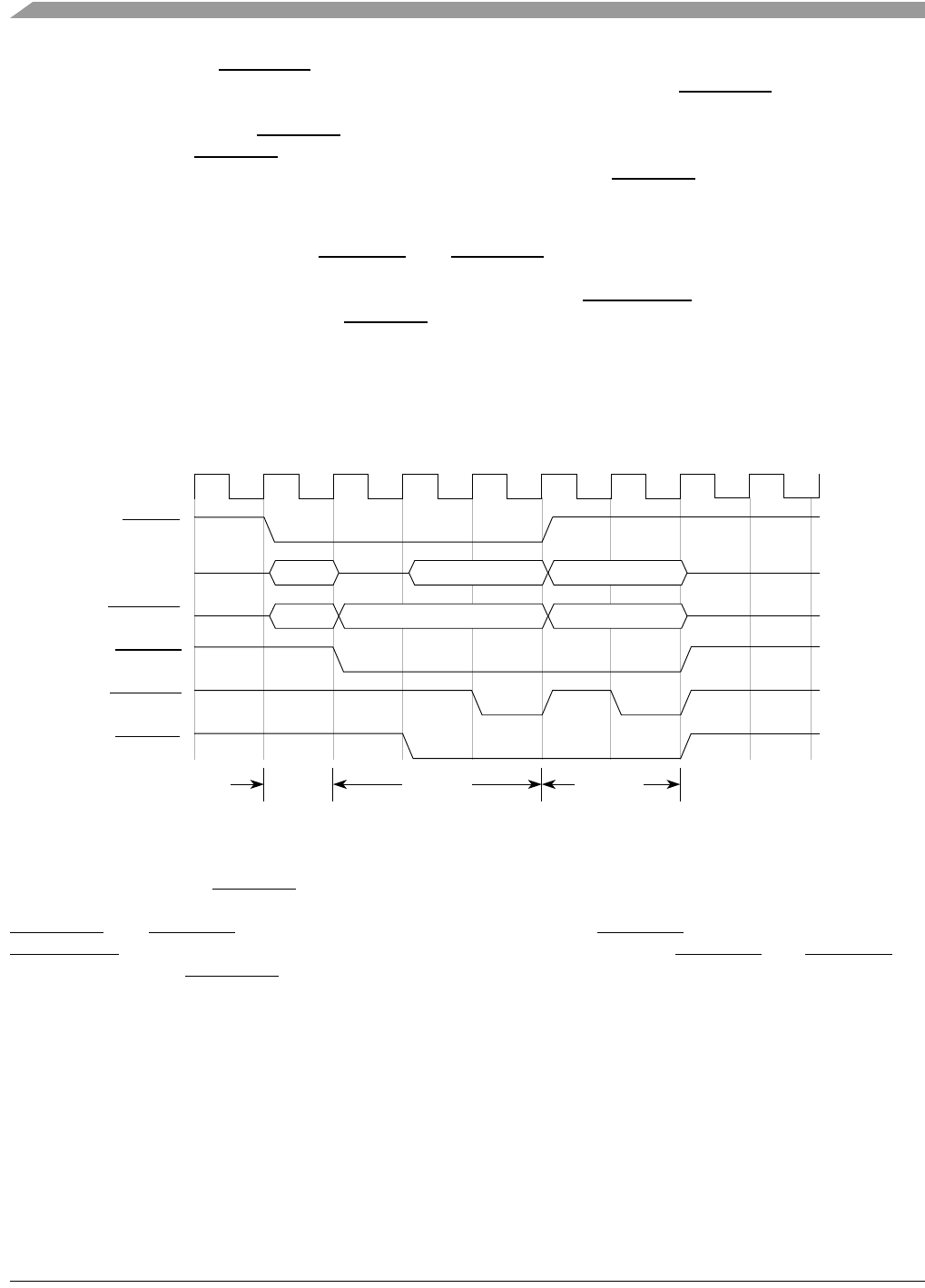
MCF548x Reference Manual, Rev. 3
19-50 Freescale Semiconductor
command driven on the PCICXBE bus. In cycle 2, the AD bus is in a turnaround cycle because of the read
on a muxed bus. The byte enables, which are active low, are driven onto the PCICXBE bus in this clock.
Any combination of byte enables can be asserted (none may be asserted). A target will respond to an
address phase by driving the DEVSEL signal. The specification allows for four types of decode operations.
The target can drive DEVSEL in 1, 2, or 3 clocks depending on whether the target is a fast, medium or
slow decode device, respectively. A single device is allowed to drive DEVSEL if no other agent responds
by the fourth clock. This is called “subtractive decoding” in PCI terminology. Note that the MCF548x is
a medium target decode device.
A valid transfer occurs when both PCIIRDY and PCITRDY are asserted. If either are negated during a
data phase, it is considered a wait state. The target asserts a wait state in cycles 3 and 5 of Figure 19-47. A
master indicates that the final data phase is to occur by negating PCIFRAME. In this diagram the target
responds as a medium device, driving DEVSEL in cycle 3.
The final data phase occurs in cycle 6. Another agent cannot start an access until cycle 8. A provision in
the specification allows the current master to start another transfer in cycle 7 when certain conditions
apply. Refer to “fast back-to-back transfers” in the PCI specification for more details.
Figure 19-47. PCI Read Terminated by Master
Figure 19-48 shows a write cycle which is terminated by the target. In this diagram the target responds as
a slow device, driving DEVSEL in cycle 4. The first data is transferred in cycle 4. The master inserts a
wait state at cycle 5. The target indicates that it can accept only one more transfer by asserting both
PCITRDY and PCISTOP at the same time in cycle 5. The signal PCISTOP must remain asserted until
PCIFRAME negates. The final data phase does not have to transfer data. If PCISTOP and PCIIRDY are
both asserted while PCITRDY is negated, it is considered a target disconnect without a transfer. See the
PCI specification for more details.
Address
Phase
PCI_CLK
FRAME
PCIAD
PCICXBE
PCIIRDY
PCITRDY
012345678
DEVSEL
Data
A1 D1 D2
CMD BYTE ENABLES
9
Phase 2
Data
Phase 1
(Wait) (Wait)
BYTE ENABLES
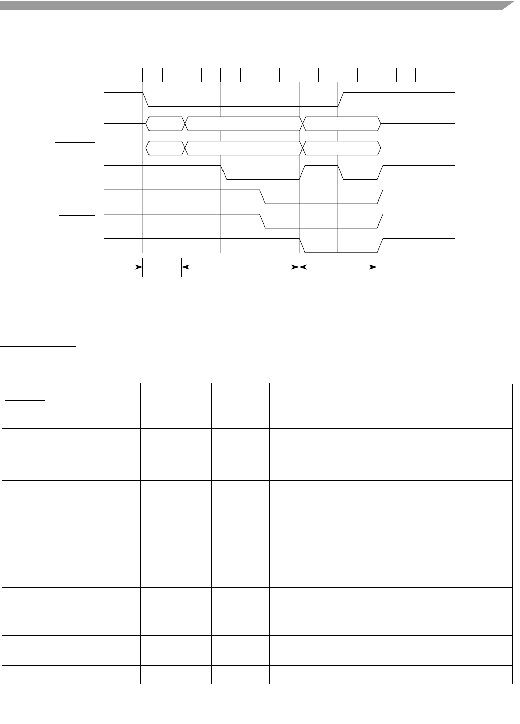
Functional Description
MCF548x Reference Manual, Rev. 3
Freescale Semiconductor 19-51
Figure 19-48. PCI Write Terminated by Target
19.4.1.4 PCI Bus Commands
PCI supports a number of different commands. These commands are presented by the initiator on the
PCICXBE[3:0] lines during the address phase of a PCI transaction.
Table 19-47. PCI Bus Commands
PCICXBE[3:0] PCI Bus
Command
MCF548x
Supports as
Initiator
MCF548x
Supports
as Target
Definition
0000 Interrupt
Acknowledge
Yes No The interrupt acknowledge command is a read (implicitly
addressing an external interrupt controller). Only one
device on the PCI bus should respond to the interrupt
acknowledge command.
0001 Special Cycle Yes No The Special Cycle command provides a mechanism to
broadcast select messages to all devices on the PCI bus.
0010 I/O read Yes No The I/O read command accesses agents mapped into the
PCI I/O space.
0011 I/O write Yes No The I/O write command accesses agents mapped into the
PCI I/O space.
0100 Reserved No No —
0101 Reserved No No —
0110 Memory-read Yes Yes The memory read command accesses agents mapped into
PCI memory space.
0111 Memory-write Yes Yes The memory write command accesses agents mapped into
PCI memory space.
1000 Reserved No No —
Address
Phase
PCISTOP
Data
Phase 2
Data
Phase 1
PCI_CLK
FRAME
PCIAD
PCICXBE
PCIIRDY
PCITRDY
012345678
DEVSEL
A1 D1 D2
CMD BYTE ENABLES
9
(Wait)
BYTE ENABLES

MCF548x Reference Manual, Rev. 3
19-52 Freescale Semiconductor
Though MCF548x supports many PCI commands as an initiator, the communication subsystem initiator
interface is intended to use PCI memory read and memory write commands.
19.4.1.5 Addressing
PCI defines three physical address spaces: PCI memory space, PCI I/O space, and PCI configuration
space. Address decoding on the PCI bus is performed by every device for every PCI transaction. Each
agent is responsible for decoding its own address. The PCI specification supports two types of address
decoding: positive decoding and subtractive decoding (refer to Section 19.4.1.5.4, “Address Decoding).
The address space that is accessed depends primarily on the type of PCI command that is used.
19.4.1.5.1 Memory Space Addressing
For memory accesses, PCI defines two types of burst ordering controlled by the two low-order bits of the
address: linear incrementing(AD[1:0] = 0b00) and cache wrap mode (AD[1:0] = 0b10). The other two
AD[1:0] encodings (0b01 and 0b11) are reserved.
For linear incrementing mode, the memory address is encoded/decoded using PCIAD[31:2]. Thereafter,
the address is incremented by 4 bytes after each data phase completes until the transaction is terminated
or completed (a 4 byte data width per data phase is implied). Note, the two low-order bits of the address
are still included in all the parity calculations.
1001 Reserved No No —
1010 Configuration
read
Yes Yes The configuration read command accesses the 256 byte
configuration space of a PCI agent.
1011 Configuration
write
Yes Yes The configuration read command accesses the 256 byte
configuration space of a PCI agent.
1100 Memory read
multiple
Yes Yes For MCF548, as master the memory read multiple
command functions the same as the memory read
command. . Cache line wrap is implemented if XL bus is the
transaction initiator and also wraps.
1101 Dual address
cycle
No No The dual address cycle command is used to transfer a
64-bit address (in two 32-bit address cycles) to 64-bit
addressable devices. MCF548 device does not respond to
this command.
1110 Memory read
line
Yes Yes The memory read line command indicates that an initiator
is requesting the transfer of an entire cache line. For
MCF548, the memory read line functions the same as the
memory read command. Cache line wrap is not
implemented.
1111 Memory write
and invalidate
Yes (DMA
access only)
Yes The memory write and invalidate command indicates that
an initiator is transferring an entire cache line, and, if this
data is in any cacheable memory, that cache line needs to
be invalidated. The memory write and invalidate functions
the same as the memory write command. Cache line wrap
is not implemented.
Table 19-47. PCI Bus Commands (Continued)
PCICXBE[3:0] PCI Bus
Command
MCF548x
Supports as
Initiator
MCF548x
Supports
as Target
Definition

Functional Description
MCF548x Reference Manual, Rev. 3
Freescale Semiconductor 19-53
As an initiator, the MCF548x supports both linear incrementing and cache wrap mode. For memory
transactions, when an XL bus burst transaction is wrapped, the cache wrap mode is automatically
generated. For zero-word-aligned bursts and single-beat transactions, the MCF548x drives AD[1:0] to
0b00.
As a target, the MCF548x treats cache wrap mode as a reserved memory mode when the cache line size
register is programmed zero. The MCF548x will return the first beat of data and then signal a disconnect
without data on the second data phase.
19.4.1.5.2 I/O Space Addressing
For PCI I/O accesses, all 32 address signals are used to provide an address with granularity of a single byte.
Once a target has claimed an I/O access, it must determine if it can complete the entire access as indicated
by the byte enable signals. If all the selected bytes are not in the address range of the target, the entire
access cannot complete. In this case, the target does not transfer any data, and terminates the transaction
with a target-abort.
19.4.1.5.3 Configuration Space Addressing and Transactions
PCI supports two types of configuration accesses. Their primary difference is the format of the address on
the PCIAD[31:0] signals during the address phase.
The two low-order bits of the address indicate the format used for the configuration address phase: type 0
(AD[1:0] = 0b00) or type 1 (AD[1:0] = 0b01). Both address formats identify a specific device and a
specific configuration register for that device:
• Type 0 configuration accesses are used to select a device on the local PCI bus. They do not
propagate beyond the local PCI bus and are either claimed by a local device or terminated with a
master-abort.
• Type 1 configuration accesses are used to target a device on a subordinate bus through a PCI-to-PCI
bridge, see Figure 19-51. Type 1 accesses are ignored by all targets except PCI-to-PCI bridges that
pass the configuration request to another PCI bus.
When the controller initiates a configuration access on the PCI bus, it places the configuration address
information on the AD bus and the configuration command on the PCICXBE[3:0] bus. A Type 0
configuration transaction is indicated by setting AD[1:0] to 0b00 during the address phase. The bit pattern
Table 19-48. PCI I/O Space Byte Decoding
Access Size PCIAD[1:0] PCICXBE[3:0] Data
8-bit 00 xxx0 AD[7:0]
01 xx01 AD[15:8]
10 x011 AD[23:16]
11 0111 AD[31:24]
16-bit 00 xxx0 AD[15:0]
01 xx01 AD[23:8]
10 x011 AD[31:16]
24-bit 00 xxx0 AD[23:0]
01 xx01 AD[31:8]
32-bit 00 xxx0 AD[31:0]

MCF548x Reference Manual, Rev. 3
19-54 Freescale Semiconductor
tells the community of devices on the PCI bus that the bridge that “owns” the PCI bus has already
performed the bus number comparison and verified that the request targets a device on its bus.
Figure 19-49 shows the contents of the AD bus during the address phase of the Type 0 configuration
access.
Figure 19-49. Type 0 Configuration Transaction:
Contents of the AD Bus During Address Phase
Address bits [10:8] identify the target function and bits AD[7:2] select one of the 64 configuration Dwords
within the target function’s configuration space. For Type 0 configuration transactions, the target device’s
IDSEL pin must be asserted. The upper 21 address lines are commonly used as IDSELs since they are not
used during the address phase of a type 0 configuration transaction.
For a Type 1 access where the target bus is a bus that is subordinate to the local PCI bus (bus 0), the
configuration transaction is still initiated on bus 0, but the bit pattern AD[1:0] indicates that none of the
devices on this bus are the target of the transaction. Rather, only PCI-to-PCI bridges residing on the local
bus should pay attention to the transaction because it targets a device on a bus further out in the hierarchy
beyond a PCI-to-PCI bridge that is attached to the local PCI bus (bus 0). This is accomplished by initiating
a Type 1 configuration transaction (setting AD[1:0] to 0b01 during the address phase). This pattern
instructs all functions other than PCI-to-PCI bridges that the transaction is not for any of them.
Figure 19-50 illustrates the contents of the AD bus during the address phase of the Type 1 configuration
access.
Figure 19-50. Type 1 Configuration Transaction:
Contents of the AD Bus During Address Phase
During the address phase of a Type 1 configuration access, the information on the AD bus is formatted as
follows:
• PCIAD[1:0] contains 0b01, identifying this as a Type 1 configuration access.
• PCIAD[7:2] identifies one of 64 configuration Dwords within the target devices’s configuration
space.
• PCIAD[10:8] identifies one of the eight functions within the target physical device.
• PCIAD[15:11] identifies one of 32 physical devices. This field is used by the bridge to select which
device’s IDSEL line to assert.
• PCIAD[23:16] identifies one of 256 PCI buses in the system.
• PCIAD[31:24] are reserved and are cleared to zero.
During a Type 1 configuration access, PCI devices ignore the state of their IDSEL inputs; PCI devices only
respond to Type 0 accesses. When any PCI-to-PCI bridge latches a Type 1 configuration access (command
= configuration read or write and AD[1:0] = 0b01) on its primary side, it must determine whether the bus
number field on the AD bus matches the number of its secondary bus or if the field is within the range of
its subordinate buses. If the bus number matches, it should claim and pass the configuration access onto
31 11 10 8 7 2 1 0
Reserved Function Number Dword Number 0 0
Target Configuration Doubleword Number
31 24 23 16 15 11 10 8 7 2 1 0
Reserved Bus Number Device Number Function Number Dword Number 0 1
Doubleword Number in the Device’s Configuration Space
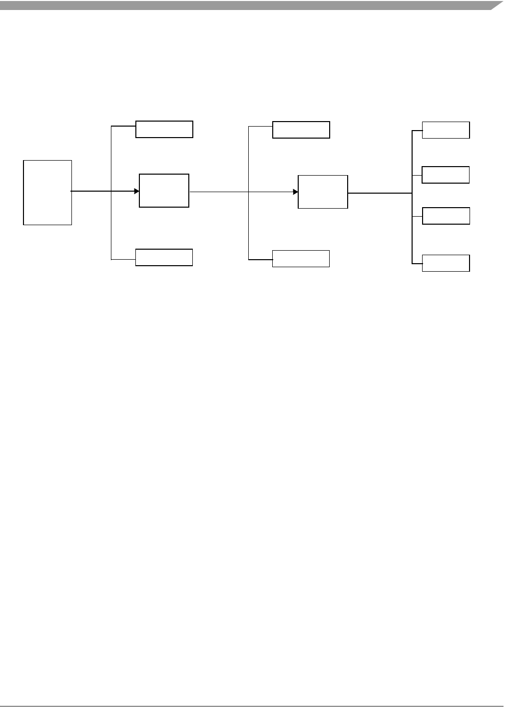
Functional Description
MCF548x Reference Manual, Rev. 3
Freescale Semiconductor 19-55
its secondary bus as a Type 0 configuration access, decoding the device number to select one of the IDSEL
lines. If the bus number is not equal to its secondary bus, but is within the range of buses that are
subordinate to the bridge, the bridge claims and passes that access through as a Type 1 access.
Figure 19-51. PCI-to-PCI Bridge Determining Match to Secondary or Subordinate Bus
19.4.1.5.4 Address Decoding
For positive address decoding, an address hits when the address on the address bus matches an assigned
address range. Multiple devices on the same PCI bus may use positive address decoding, though there
cannot be any overlap in the assigned address ranges. The MCF548x only implements positive address
decoding.
For subtractive address decoding, an address hits when the address on the address bus does not match any
address range for any of the PCI devices on the bus. Only one device on a PCI bus may use subtractive
address decoding, and its use is optional.
19.4.2 Initiator Arbitration
There are three possible internal initiator sources: comm bus transmit, comm bus receive, or the XL bus
(from the internal system arbiter). Custom interface logic arbitrates and provides multiplex selection
control for these sources to the PCI controller. Figure 19-52 illustrates the arbitration block connection.
PCI
Bridge
PCI
Bridge
Secondary
Bus Subordinate
Bus
Primary
Bus
MCF548x .
Device 0.0
.
Device 1.0
Device 0.1
Device 1.1
Device 0.2
Device 1.2
Device 2.2
Device 3.2
Responds
to Type 0
Responds
to Type 0
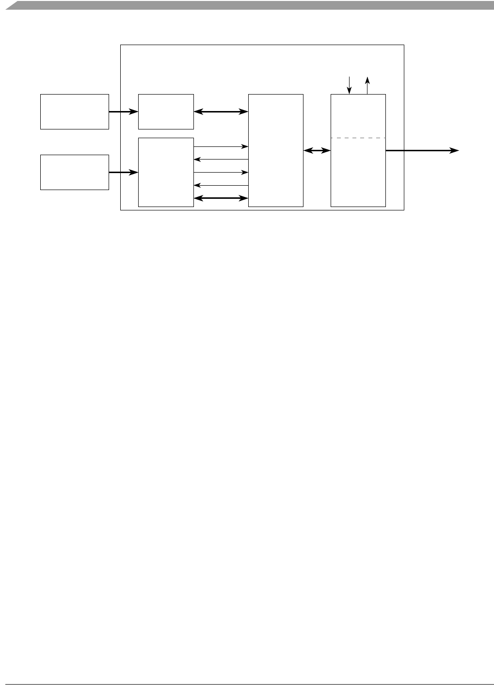
MCF548x Reference Manual, Rev. 3
19-56 Freescale Semiconductor
Figure 19-52. Initiator Arbitration Block Diagram
19.4.2.1 Priority Scheme
The PCI initiator arbiter uses the following fixed priority scheme:
1. XL bus initiator
2. Comm bus transmit (Tx)
3. Comm bus receive (Rx) (lowest)
19.4.3 Configuration Interface
The PCI bus protocol requires the implementation of a standardized set of registers for most devices on
the PCI bus. The MCF548x implements a Type 0 Configuration register set or header. These registers,
discussed in Section 19.3.1, “PCI Type 0 Configuration Registers,” are primarily intended to be read or
written by the PCI configuring master at initialization time through the PCI bus. The MCF548x provides
internal access to these registers through a slave bus interface. As with most MCF548x registers, they are
accessible by software in the address space at offsets of MBAR. Internal accesses to the Type 0
Configuration header do not require PCI arbitration when they are accessed as offsets of MBAR and are
allowed to execute regardless of whether any write data is posted in the PCI Controller.
If the MCF548x is the configuring master, the slave bus interface should be used to configure the PCI
Controller. An external master would configure the PCI controller through the external PCI bus.
More information on the standard PCI Configuration register can be found in the PCI 2.2 specification.
19.4.4 XL Bus Initiator Interface
The processor core or internal masters may access the PCI bus via the XL bus initiator interface. This
internal interface is accessed through three windows in MCF548x address space set up by base address and
base address mask registers (Section 19.3.2.5, “Initiator Window 0 Base/Translation Address Register
(PCIIW0BTAR)”). The base address registers must be enabled by setting their respective enable bits in
the Section 19.3.2.8, “Initiator Window Configuration Register (PCIIWCR).” Accesses to this area are
translated into PCI transactions on the PCI bus. See Section 19.5.2, “Address Maps,” for examples on
setting up address windows.
rx_req
rx_gnt
tx_gnt
tx_req
PCI
Request/Grant
(to PCI Arbiter)
External
PCI Bus
PCI
Initiator
Arbiter
Comm Bus
Initiator
XL Bus
Initiator
XL Bus
Arbiter
Multichannel
DMA
Controller
PCI
Controller
Initiator
Interface

Functional Description
MCF548x Reference Manual, Rev. 3
Freescale Semiconductor 19-57
The particular type of PCI transaction generated is determined by the PCI configuration bits associated
with the address window (PCIIWCR). For example, the user might set one window to do PCI memory read
multiple accesses, one window for PCI I/O accesses, and the other window to do non-prefetchable
(memory-mapped I/O) PCI memory accesses. See Table 19-57 for command translations.
In addition to the configurable address window mapping logic, the register interface provides a
configuration address register, which provides the ability to generate configuration, interrupt
acknowledge, and special cycles. External PCI devices should be configured through this interface. See
Section 19.4.4.2, “Configuration Mechanism” for configuration, interrupt acknowledge, and special cycle
command support.
The PCI XL bus initiator interface supports all XL bus transactions, including single-beat transfers and
bursts (32 bytes). Single-beat 64-bit data transactions are automatically translated into 2-beat burst
transfers on the PCI bus.
Standard XL bus burst transactions are supported as well, however, buffering is implemented to boost
performance during writes and avoid deadlock scenario for all reads and memory writes. If the target for
an XL bus read from PCI disconnects part way through the burst, the MCF548may have to handle a local
memory access from an alternate PCI master before the disconnected transfer can continue.
XL bus initiator read requests are decoded into four types: PCI Memory, I/O, Configuration, and Interrupt
Acknowledge. The PCI Controller must first gain access to the PCI bus before acknowledging the XL bus
read request. The specific timing of the address acknowledge is dependent upon the type of transfer.
When the XL bus requests burst data from PCI space, the data received from PCI is stored in a 32-byte
read buffer. The PCI Controller does not terminate the address tenure of the XL bus transaction until all
requested data is latched. This is because PCI targets are allowed to disconnect in the middle of a transfer,
and the XL bus requires burst transfers to be atomic. If the PCI target disconnects in the middle of the data
transfer and an alternate PCI master acquires the bus and initiates a local memory access, the Controller
retries the internal read transaction on the XL bus. The PCI Controller continues to request mastership of
the PCI bus until the original request is completed.
For example, if the XL bus initiates a burst read, and the PCI target disconnects after transferring the first
half of the burst, the MCF548x re-arbitrates for the PCI bus, and when granted, initiates a new transaction
with the address of the third beat of the burst (4-beat XL bus bursts). If an alternate PCI master requests
data from local memory while the PCI Controller is waiting for the PCI bus grant, the PCI controller retries
the XL bus transaction to allow the PCI-initiated transaction to complete and the read buffer will be
emptied. Transactions are not reordered, but taken first come, first served.
When the MCF548x is acting as in initiator/master, PCI critical-word-first (CWF) burst operation (i.e.
cache line wrap burst) is supported, and the 2-bit cache line wrap address mode is driven on the address
bus when the XL bus starts the burst at a non-zero-word-first address. Note that this option is only provided
as a means for the initiator to support memory targets that support cache-line wrap. The processor is not
permitted to cache from memory targets residing on the PCI bus in the 2.2 spec.
XL bus writes are decoded into PCI memory, PCI I/O, PCI configuration, or special cycles. If the
transaction decodes into an I/O, configuration, or special cycle, the write is connected. The PCI controller
gains access to the PCI bus and successfully transfers the data before it asserts address acknowledge to the
XL bus. If the address maps to PCI memory space, the XL bus address tenure is immediately
acknowledged and write data is posted.
A 32-byte write buffer is used to post memory writes from XL bus to PCI. Buffering minimizes the effect
of the slower PCI bus on the higher-speed XL bus. It may contain single-beat XL bus write transactions or
a single burst. After the XL bus write data is latched internally, the bus is available for subsequent
transactions without having to wait for the write to the PCI target to complete. If a subsequent XL bus write

MCF548x Reference Manual, Rev. 3
19-58 Freescale Semiconductor
request to the PCI bus comes in, the data transfer is delayed until all previous writes to the PCI bus are
completed. Only when the write buffer is empty can burst data from the XL bus be posted.
19.4.4.1 Endian Translation
The PCI bus is inherently little endian in its byte ordering. The internal XL bus, however, is big endian.
XL bus transactions are limited to 1, 2, 3, 4, 5, 6, 7, 8, or 32 byte (burst) transactions within the data bus
byte lanes on any 32-bit address boundary for burst transfers. Table 19-49 shows the byte lane mapping
between the two buses.
Table 19-49. XL Bus to PCI Byte Lanes for Memory1 Transactions
XL Bus PCI Bus
A[29:31
]
TSIZ
[0:2]
Data Bus Byte Lanes AD
[2:0]
BE[3:
0]
31:2
4
23:1
615:8 7:0
0123456 7
000 001 OP7 —————— — 000 1110 ———OP7
001 001 —OP7 — — — — — — 000 1101 — — OP7 —
010 001 — — OP7 — — — — — 000 1011 —OP7 — —
011 001 — — — OP7 — — — — 000 0111 OP7 — — —
100 001 — — — — OP7 — — — 100 1110 ———OP7
101 001 —————OP7 — — 100 1101 — — OP7 —
110 001 — — — — — — OP7 —100 1011 —OP7 — —
111 001 ———————OP7 100 0111 OP7 — — —
000 010 OP6 OP7 — — — — — — 000 1100 — — OP7 OP6
001 010 —OP6 OP7 — — — — — 000 1001 —OP7 OP6 —
010 010 — — OP6 OP7 — — — — 000 0011 OP7 OP6 — —
011 010 — — — OP6 OP7 — — — 000 0111 OP6 — — —
100 1110 ———OP7
100 010 — — — — OP6 OP7 — — 100 1100 — — OP7 OP6
101 010 —————OP6 OP7 —100 1001 —OP7 OP6 —
110 010 — — — — — — OP6 OP7 100 0011 OP7 OP6 — —
000 011 OP5 OP6 OP7 — — — — — 000 1000 —OP7 OP6 OP5
001 011 —OP5 OP6 OP7 — — — — 000 0001 OP7 OP6 OP5 —
010 011 — — OP5 OP6 OP7 — — — 000 0011 OP6 OP5 — —
100 1110 ———OP7
011 011 — — — OP5 OP6 OP7 — — 000 0111 OP5 — — —
100 1100 — — OP7 OP6
100 011 — — — — OP5 OP6 OP7 —100 1000 —OP7 OP6 OP5
101 011 —————OP5 OP6 OP7 00 0001 OP7 OP6 OP5 —

Functional Description
MCF548x Reference Manual, Rev. 3
Freescale Semiconductor 19-59
000 100 OP4 OP5 OP6 OP7 — — — — 00 0000 OP7 OP6 OP5 OP4
001 100 —OP4 OP5 OP6 OP7 — — — 000 0001 OP6 OP5 OP4 —
100 1110 ———OP7
010 100 — — OP4 OP5 OP6 OP7 — — 000 0011 OP5 OP4 — —
100 1100 — — OP7 OP6
011 100 — — — OP4 OP5 OP6 OP7 —000 0111 OP4 — — —
100 1000 —OP7 OP6 OP5
100 100 — — — — OP4 OP5 OP6 OP7 100 0000 OP7 OP6 OP5 OP4
000 101 OP3 OP4 OP5 OP6 OP7 — — — 000 0000 OP6 OP5 OP4 OP3
100 1110 ———OP7
001 101 —OP3 OP4 OP5 OP6 OP7 — — 000 0001 OP5 OP4 OP3 —
100 1100 — — OP7 OP6
010 101 — — OP3 OP4 OP5 OP6 OP7 —000 0011 OP4 OP3 — —
100 1000 —OP7 OP6 OP5
011 101 — — — OP3 OP4 OP5 OP6 OP7 000 0111 OP3 — — —
100 0000 OP7 OP6 OP5 OP4
000 110 OP2 OP3 OP4 OP5 OP6 OP7 — — 000 0000 OP5 OP4 OP3 OP2
100 1100 — — OP7 OP6
001 110 —OP2 OP3 OP4 OP5 OP6 OP7 —000 0001 OP4 OP3 OP2 —
100 1000 —OP7 OP6 OP5
010 110 — — OP2 OP3 OP4 OP5 OP6 OP7 000 0011 OP3 OP2 — —
100 0000 OP7 OP6 OP5 OP4
000 111 OP1 OP2 OP3 OP4 OP5 OP6 OP7 —000 0000 OP4 OP3 OP2 OP1
100 1000 —OP7 OP6 OP5
001 111 —OP1 OP2 OP3 OP4 OP5 OP6 OP7 000 0001 OP3 OP2 OP1 —
100 0000 OP7 OP6 OP5 OP4
000 000 OP0 OP1 OP2 OP3 OP4 OP5 OP6 OP7 000 0000 OP3 OP2 OP1 OP0
100 0000 OP7 OP6 OP5 OP4
1The byte lane translation will be similar for other types of transactions. However, the PCI address may be different
as explained in Section 19.4.1.5, “Addressing.”
Table 19-49. XL Bus to PCI Byte Lanes for Memory1 Transactions (Continued)
XL Bus PCI Bus
A[29:31
]
TSIZ
[0:2]
Data Bus Byte Lanes AD
[2:0]
BE[3:
0]
31:2
4
23:1
615:8 7:0
0123456 7

MCF548x Reference Manual, Rev. 3
19-60 Freescale Semiconductor
19.4.4.2 Configuration Mechanism
In order to support both Type 0 and Type 1 configuration transactions, the MCF548x provides the 32 bit
configuration address register (PCICAR). The register specifies the target PCI bus, device, function, and
configuration register to be accessed. A read or a write to the MCF548x window defined as PCI I/O space,
in PCIIWCR, causes the host bridge to translate the access into a PCI configuration cycle if the enable bit
in the configuration address register is set and the device number does not equal 0b1_1111. For space to
be defined as I/O space, the accessed space (one of the initiator windows) must be programmed as I/O, not
memory. See Section 19.3.2.8, “Initiator Window Configuration Register (PCIIWCR)”.
The format of the configuration address register is shown in Section 19.3.2.11, “Configuration Address
Register (PCICAR)”.When the MCF548x detects an access to an I/O window, it checks the enable flag and
the device number in the configuration address register. If the enable bit is set, and the device number is
not 0b1_1111, the MCF548x performs a configuration cycle translation function and runs a configuration
read or configuration write transaction on the PCI bus. The device number 0b1_1111 is used for
performing interrupt acknowledge and special cycle transactions. See Section 19.4.4.3, “Interrupt
Acknowledge Transactions,” and Section 19.4.4.4, “Special Cycle Transactions,” for more information. If
the bus number corresponds to the local PCI bus (bus number = 0x00), a Type 0 configuration cycle
transaction is performed. If the bus number indicates a remote PCI bus, the MCF548x performs a Type 1
configuration cycle translation. If the enable bit is not set, the access to the configuration window is passed
through to the PCI bus as an I/O transfer (window translation applies).
Note that the PCI data byte enables (PCICXBE[3:0]) are determined by the size access to the window.
19.4.4.2.1 Type 0 Configuration Translation
Figure 19-53 shows the Type 0 translation function performed on the contents of the configuration address
register to the AD[31:0] signals on the PCI bus during the address phase of the configuration cycle (this
only applies when the enable bit in the configuration address register is set).
Figure 19-53. Type 0 Configuration Translation
For Type 0 configuration cycles, the MCF548x translates the device number field of the configuration
address register into a unique IDSEL line shown in Table 19-50. It allows for 21 different devices.
Table 19-50. Type 0 Configuration Device Number to IDSEL Translation
Device Number
IDSEL
Binary Decimal
0b0_0000-0b0_100110–9 -
0b0_1010 10 AD31
31 30 24 23 16 15 11 10 8 7 2 1 0
E Reserved Bus Number Device Number Function Number Dword Rsvd
Contents of Configuration Address Register:
31 11 10 2 1 0
IDSEL (Only One Signal High) Function Number/Dword 0 0
PCIAD[31:0] Signals During Address Phase:
See Table 19-50

Functional Description
MCF548x Reference Manual, Rev. 3
Freescale Semiconductor 19-61
The MCF548x can issue PCI configuration transactions to itself. A Type 0 configuration initiated by the
MCF548x can access its own configuration space by asserting its IDSEL input signal.
NOTE
Asserting IDSEL is the only way the MCF548x can clear its own status
register (PCISCR) bits (read-write-clear).
For Type 0 translations, the function number and Dword fields are copied without modification onto the
AD[10:2] signals, and AD[1:0] are driven low during the address phase.
0b0_1011 11 AD11
0b0_1100 12 AD12
0b0_1101 13 AD13
0b0_1110 14 AD14
0b0_1111 15 AD15
0b1_0000 16 AD16
0b1_0001 17 AD17
0b1_0010 18 AD18
0b1_0011 19 AD19
0b1_0100 20 AD20
0b1_0101 21 AD21
0b1_0110 22 AD22
0b1_0111 23 AD23
0b1_1000 24 AD24
0b1_1001 25 AD25
0b1_1010 26 AD26
0b1_1011 27 AD27
0b1_1100 28 AD28
0b1_1101 29 AD29
0b1_1110 30 AD30
0b1_1111 31 -
1Device numbers 0b0_0000 to 0b0_1001 are reserved. Programming to
these values and issuing a configuration transaction will result in a PCI
configuration cycle with AD31-AD11 driven low.
Table 19-50. Type 0 Configuration Device Number to IDSEL Translation (Continued)
Device Number
IDSEL
Binary Decimal

MCF548x Reference Manual, Rev. 3
19-62 Freescale Semiconductor
19.4.4.2.2 Type 1 Configuration Translation
For Type 1 translations, the 30 high-order bits of the configuration address register are copied without
modification onto the AD[31:2] signals during the address phase. The AD[1:0] signals are driven to 0b01
during the address phase to indicate a Type 1 configuration cycle.
19.4.4.3 Interrupt Acknowledge Transactions
When the MCF548x detects a read from an I/O defined window (Section 19.3.2.8, “Initiator Window
Configuration Register (PCIIWCR)”), it checks the enable flag, bus number, and the device number in the
configuration address register (Section 19.3.2.11, “Configuration Address Register (PCICAR)”). If the
enable bit is set, the bus number corresponds to the local PCI bus (bus number = 0x00), and the device
number is all 1’s (device number = 0b1_1111), then an interrupt acknowledge transaction is initiated. If
the bus number indicates a subordinate PCI bus (bus number != 0x00), a Type 1 configuration cycle is
initiated, similar to any other configuration cycle for which the bus number does not match. The function
number and Dword values are ignored.
The interrupt acknowledge command (0b0000) is driven on the PCICXBE[3:0] signals and the address bus
is driven with a stable pattern during the address phase, but a valid address is not driven. The address of
the target device during an interrupt acknowledge is implicit in the command type. Only the system
interrupt controller on the PCI bus should respond to the interrupt acknowledge and return the interrupt
vector on the data bus during the data phase. The size of the interrupt vector returned is indicated by the
value driven on the PCICXBE[3:0] signals.
19.4.4.4 Special Cycle Transactions
When the MCF548x detects a write to an I/O defined window (Section 19.3.2.8, “Initiator Window
Configuration Register (PCIIWCR)”), it checks the enable flag, bus number, and the device number in the
configuration address register (Section 19.3.2.11, “Configuration Address Register (PCICAR)”). If the
enable bit is set, the bus number corresponds to the local PCI bus (bus number = 0x00), and the device
number is all 1’s (device number = 0b1_1111), then a Special Cycle transaction is initiated. If the bus
number indicates a subordinate PCI bus (where the bus number field is not 0x00), a Type 1 configuration
cycle is initiated, similar to any other configuration cycle for which the bus number does not match. The
function number and Dword values are ignored.
The Special Cycle command (0b0001) is driven on the PCICXBE[3:0] signals and the address bus is
driven with a stable pattern during the address phase, but contains no valid address information. The
Special Cycle command contains no explicit destination address, but broadcast to all agents on the same
bus segment. Each receiving agent must determine whether the message is applicable to it. PCI agent will
never assert DEVSEL in response to a Special Cycle command. Master Abort is the normal termination
for a Special Cycle and no errors are reported for this case of Master Abort termination. This command is
basically a broadcast to all agents, and interested agents accept the command and process the request.
Note, Special Cycle commands do not cross PCI-to-PCI bridges. If a master wants to generate a Special
Cycle command on a specific bus in the hierarchy that is not its local bus, it must use a Type 1
configuration write command to do so. Type 1 configuration write commands can traverse PCI-to-PCI
bridges in both directions for the purpose of generating Special Cycle commands on any bus in the
hierarchy and are restricted to a single data phase in length. However, the master must know the specific
bus on which it desires to generate the Special Cycle command and cannot simply do a broadcast to one
bus and expect it to propagate to all buses.
During the data phase, PCIAD[31:0] contain the Special Cycle message and an optional data field. The
Special Cycle message is encoded on the 16 least significant bits (PCIAD[15:0]) and the optional data field
is encoded on the most significant bits (PCIAD[31:16]). The Special Cycle message encodings are

Functional Description
MCF548x Reference Manual, Rev. 3
Freescale Semiconductor 19-63
assigned by the PCI SIG Steering Committee. The current list of defined encodings are provided in
Table 19-51.
19.4.4.5 Transaction Termination
If the PCI cycle Master Aborts, the interface will return 0xFFFF FFFF as read data, but complete without
error. It will issue an interrupt to the internal interrupt controller if enabled.
For abnormal transaction termination during an XL bus-initiated transaction ( retry limit reached or target
abort), an error (TEA on XL bus) is generated. It will issue an interrupt to the MCF548x interrupt controller
if such interrupts are enabled.
Transfers that cross the 32-bit boundary (greater than 4 bytes) to a PCI nonmemory address range result
in a transfer error (TEA on XL bus).. The space is defined as nonmemory if the IO/M# configuration bit
associated with that window is programmed “0”.This type of unsupported transfer does not cause an
interrupt.
19.4.5 XL Bus Target Interface
This section discusses the MCF548x as a PCI target, and as such, the following apply:
• The target interface can issue target abort, target retry, and target disconnect terminations.
• The target interface supports fast back-to-back cycles.
• No support of dual address cycles as a PCI target.
• Target transactions are not snooped by the processor.
• Medium device selection timing only.
• Three 32-byte buffers enhance data throughput.
The XL bus Target Interface provides access for external PCI masters to two windows of MCF548x
address space. Target Base Address Translation Registers 0 and 1 allow the user to map PCI address hits
on MCF548x PCI Base Address Registers to areas in the internal address space. All of these registers must
be enabled for this interface to operate.
Table 19-51. Special Cycle Message Encodings
PCIAD[15:0] Message
0x0000 SHUTDOWN
0x0001 HALT
0x0002 x86 architecture-specific
0x0003–0xFFFF —
Table 19-52. Unsupported XL Bus Transfers
XL Bus Transaction PCI Address Space
Burst (32-byte) Nonmemory
> 4 byte Single Beat Nonmemory
4 byte Single Beat at a[29:31] 001, 010, or 011 Nonmemory
3 byte Single Beat at a[29:31] 010 or 011 Nonmemory
2 byte Single Beat at a[29:31] 011 Nonmemory

MCF548x Reference Manual, Rev. 3
19-64 Freescale Semiconductor
Upon detection of a PCI address phase, the PCI controller decodes the address and bus command to
determine if the transaction is for local memory (BAR0 or BAR1 hit). If the transaction falls within
MCF548x PCI space (memory only), the PCI Controller target interface asserts DEVSEL, latches the
address, decodes the PCI bus command, and forwards them to the internal control unit. On writes, data is
forwarded along with the byte enables to the internal gasket. On reads, four bytes of data are provided to
the PCI bus and the byte enables determine which byte lanes contain meaningful data. If no byte enables
are asserted, MCF548x completes a read access with valid data and completes a write access by discarding
the data internally. All target transactions will be translated into XL bus master transactions.
There are two address translation registers that must be initialized before data transfer can begin. These
address registers correspond to BAR0 and BAR1 in MCF548x PCI Type 00h Configuration space register
(PCI space). When there is a hit on MCF548x PCI base address ranges (0 or 1), the upper bits of the address
are written over by this register value to address some space in MCF548x. One 256-Kbyte base address
range (BAR0) maps to non-prefetchable local memory and one 1-Gbyte range (BAR1) targeted to
prefetchable memory.
19.4.5.1 Reads from Local Memory
MCF548x can provide continuous data to a PCI master using two 32-byte buffers. The PCI controller
bursts reads internally at each 32-byte PCI address boundary. The data is stored in the first 32-byte buffer
until either the PCI master flushes the data or the transaction terminates (PCIFRAME deasserts). For
prefetchable memory (BAR1 space), the next line can be fetched from memory in anticipation of the next
PCI request and stored in the second buffer. Prefetching is performed for BAR1 addressed transactions if
the PCI command is a Memory Read Multiple or the prefetch bit is set in the Target Control Register
(PCITCR).
19.4.5.2 Local Memory Writes
The target interface always posts writes. This allows for data to be latched while waiting for internal access
to local memory.While PCI burst transactions are accepted, writes are sent out on the internal bus as
single-beat. A 32-byte posted write buffer is implemented to improve data throughput.
If the PCI controller aborts the transaction in the middle of PCI burst due to internal conflicts, the external
master recognizes some of the data as transferred. (Subsequent transfers of a burst will be aborted on PCI
bus). The external PCI master must query the “Target abort signalled” bit in the PCI Type 00h
configuration status register to determine if a target abort occurred.
19.4.5.3 Data Translation
The XL bus supports misaligned operations, however, it is strongly recommended that software attempt to
transfer contiguous code and data where possible. Non-contiguous transfers degrade performance.
PCI-to-XL bus transaction data translation is shown in Table 19-53 and Table 19-54.

Functional Description
MCF548x Reference Manual, Rev. 3
Freescale Semiconductor 19-65
Table 19-53. Aligned PCI to XL Bus Transfers
PCI Bus XL Bus
BE[3:
0] AD[2:0] 31:24 23:16 15:8 7:0 A[29:31]
Data Bus Byte Lanes
01234567
1110 000 OP3 000 OP3
1101 000 OP3 001 OP3
1011 000 OP3 010 OP3
0111 000 OP3 011 OP3
1110 100 OP3 100 OP3
1101 100 OP3 101 OP3
1011 100 OP3 110 OP3
0111 100 OP3 111 OP3
1100 000 OP3 OP2 000 OP2 OP3
1001 000 OP3 OP2 001 OP2 OP3
0011 000 OP3 OP2 010 OP2 OP3
1100 100 OP3 OP2 100 OP2 OP3
1001 100 OP3 OP2 101 OP2 OP3
0011 100 OP3 OP2 110 OP2 OP3
1000 000 OP3 OP2 OP1 000 OP1 OP2 OP3
0001 000 OP3 OP2 OP1 001 OP1 OP2 OP3
1000 100 OP3 OP2 OP1 100 OP1 OP2 OP3
0001 100 OP3 OP2 OP1 101 OP1 OP2 OP3
0000 000 OP3 OP2 OP1 OP0 000 OP0 OP1 OP2 OP3
0000 100 OP3 OP2 OP1 OP0 100 OP0 OP1 OP2 OP3
Table 19-54. Non-Contiguous PCI to XL Bus Transfers (Requires Two XL Bus Accesses)
PCI Bus XL Bus
BE[3:
0] AD[2:0] 31:24 23:16 15:8 7:0 A[29:31]
Data Bus Byte Lanes
01234567
1010 000 OP3 OP2 000 OP2
010 OP3
1010 100 OP3 OP2 100 OP2
110 OP3

MCF548x Reference Manual, Rev. 3
19-66 Freescale Semiconductor
19.4.5.4 Target Abort
A target abort will occur if the PCI address falls within a base address window (BAR0 or BAR1) that has
not been enabled. See Section 19.3.2.2, “Target Base Address Translation Register 0 (PCITBATR0),” and
Section 19.3.2.3, “Target Base Address Translation Register 1 (PCITBATR1).”
19.4.5.5 Latrule Disable
The latrule disable bit in the interface control register, Section 19.3.2.4, “Target Control Register
(PCITCR),” prevents the PCI controller from automatically disconnecting a target transaction due to the
PCI 16/8 clock rule. With this bit set, it is possible to hang the PCI bus if the internal bus does not complete
the data transfer.
19.4.6 Communication Subsystem Initiator Interface
This interface provides for high-speed, autonomous DMA transactions to PCI with the PCI controller
operating as a standard communication subsystem peripheral. Full duplex operation is supported and direct
XL bus transactions can also be interleaved while comm bus transactions are in progress. Internal
arbitration will occur continuously to support transaction interleaving. (Section 19.4.2, “Initiator
Arbitration”) Multichannel DMA operation operates independently of the XL bus. Non-PCI transactions
0110 000 OP3 OP2 000 OP2
011 OP3
0110 100 OP3 OP2 100 OP2
111 OP3
0101 000 OP3 OP2 001 OP2
011 OP3
0101 100 OP3 OP2 101 OP2
111 OP3
0010 000 OP3 OP2 OP1 000 OP1
010 OP2 OP3
0010 100 OP3 OP2 OP1 100 OP1
110 OP2 OP3
0100 000 OP3 OP2 OP1 000 OP1 OP2
011 OP3
0100 100 OP3 OP2 OP1 100 OP1 OP2
111 OP3
Table 19-54. Non-Contiguous PCI to XL Bus Transfers (Requires Two XL Bus Accesses) (Continued)
PCI Bus XL Bus
BE[3:
0] AD[2:0] 31:24 23:16 15:8 7:0 A[29:31]
Data Bus Byte Lanes
01234567

Functional Description
MCF548x Reference Manual, Rev. 3
Freescale Semiconductor 19-67
on the XL bus will have 100% bandwidth available to them during PCI multichannel DMA activities. In
general, this block will be used by functions in the multichannel DMA API.
The communication subsystem initiator interface consists of Receive and Transmit FIFOs, integrated as
separate multichannel DMA peripherals. Therefore, it is generally controlled by the multichannel DMA
controller through a pre-described program loop. As with all communication subsystem peripherals, it can
be accessed and controlled directly through the slave bus interface if desired, but this path does not
generally lend itself to high throughput.
The Transmit and Receive FIFOs are 32 × 36 bits and support PCI bursts up to 8 beats. This burst size is
programmable. The general approach is to write a PCI command and address to the control register along
with the number of bytes to be transmitted (Packet_Size).
When transmitting data, the module will wait for the Transmit FIFO to fill and then begin transmitting the
data onto the PCI bus. Multichannel DMA must handle filling the Transmit FIFO to support the specified
number of bytes. Transmission will continue until the specified number of bytes have been sent.
When reading data, the module will check that enough space is available in the Receive FIFO and
immediately begin PCI read transactions. Multichannel DMA must handle emptying the Receive FIFO to
support the specified number of bytes. Transmission will continue until the specified number of bytes have
been received.
At this point, software must restart the procedure by at least re-writing the Packet_Size register. Each
transmission of the specified number of bytes is considered a “packet”. A new packet can be instructed to
continue at the last valid PCI address or software may choose to write a new starting address. The largest
burst size is 8 and the largest Packet_Size is 65,532, so a packet will typically consist of many PCI data
bursts.
The Transmit Controller will wait until sufficient bytes are in the Transmit FIFO to support a full burst and
will continue in this mode until the entire packet is transmitted. Similarly, the Receive Controller will stall
until sufficient space is available in the Receive FIFO to support a full burst. If the packet is nearly done
and the number of bytes remaining to complete the packet is less than Max_beats, the remaining data will
be performed as single-beat PCI transactions.
19.4.6.1 Access Width
This multichannel DMA module primarily performs 32-bit data accesses to and from PCI, even though
some signals are referred to in bytes. The two least significant bits of the PCITPSR and PCIRPSR value
are ignored. All PCI byte enables are enabled during these types of accesses. Additionally, the FIFOs
should only be accessed using 32-bit accesses.
The communication subsystem interface optionally supports 16 bit accesses on the PCI bus. Because reads
and writes to and from the FIFO require 32-bit accesses, using this option requires padding the remaining
16 bits of data.
19.4.6.2 Addressing
The communication subsystem initiator interface does not use the addressing windows that are set up for
the XL bus initiator interface. Instead, the Tx Start Address register and Rx Start Address register are used.
Software programs these registers with the initial starting address for the packet. The module contains an
internal counter which will present the incremented PCI address at the beginning of each successive burst
for packet transfers.
If the Disable Increment bit is set, the PCI controller will present the same address during the address phase
of each PCI transaction throughout the entire packet transmission.

MCF548x Reference Manual, Rev. 3
19-68 Freescale Semiconductor
19.4.6.3 Data Translation
The PCI bus is inherently little endian in its byte ordering. The comm bus however is big endian.
Table 19-55 shows the byte lane mapping between the two buses. Because this interface only allows 32-bit
accesses, there is only one entry.
19.4.6.4 Initialization
The following list is the recommended procedure for setting up either the Transmit or Receive controller.
1. Set the Start Address
2. Set the PCI command, Max_Retries, and Max_Beats
3. Set mode, Continuous or Non-continuous
4. Reset the FIFO
5. Set the FIFO Alarm and Granularity fields
6. Set the Master Enable bit
7. Set the Reset Controller bit low
8. Write the Packet Size value to begin the transfer
19.4.6.5 Restart and Reset
This section describes Restart and Reset operation for both the Transmit and Receive controllers of the
communications subsystem interface.
A Restart sequence is required whenever the controller ends a packet transmission, either normally or
abnormally. In non-continuous mode, a new Start_Add value is generally required since this value is
re-used as the start of the next packet once it is Restarted. In Continuous mode, the Start_Add value is not
reused. Instead, the next packet begins where the last one left off, but a Restart sequence is still required
to get this next packet started.
Writing a non-zero value to the Packet_Size register generates a Restart pulse to the controller. If the
Master Enable bit is low when the Packet_Size register is written, the Restart pulse will occur when the
Master Enable bit is programmed high. Depending on the desired mode of operation other register accesses
may be required, as described in the following paragraphs.
If Continuous mode is not selected, operation is fairly straight forward. Upon packet termination, Restart
will not occur until Packet_Size is written with a non-zero value, even if the packet size is the same it must
be re-written. The Master Enable bit was previously high and can remain so. The Reset Controller bit was
previously low and can remain so. Toggling the Master Enable or Reset bit is unnecessary but would not
disrupt the transmit controller. If any other Control values, e.g. Start_Add, are to be changed they should
be written either prior to writing the Packet_Size value or written while the Master Enable bit is negated
and the Reset Controller bit is negated. The recommended approach is to write the control values in order
(Packet_Size must be last) and not toggle the Master Enable bit. The Reset bit should remain negated.
Table 19-55. Comm Bus to PCI Byte Lanes for Memory Transactions
Transfer
Comm Bus PCI Data Bus
cAddress
[1:0]
cByte
Enable
[3:0]
Data Bus PCIAD
[1:0]
BE
[3:0]
Data Bus
31:24 23:16 15:8 7:0 31:24 23:16 15:8 7:0
long 00 1111 OP0 OP1 OP2 OP3 00 0000 OP3 OP2 OP1 OP0

Functional Description
MCF548x Reference Manual, Rev. 3
Freescale Semiconductor 19-69
If Continuous mode is active, basic operation is still straight forward. A Restart is achieved by writing the
Packet_Size register to a non-zero value (just as before). When a Restart occurs, the Bytes_Done counter
is cleared to begin counting for the current packet and the Packets_Done counter increments. The
Packets_Done counter indicates the total number of previously completed packets. However, the Master
Enable and Reset bits must not toggle in this case. If the Master Enable bit goes low the Packets_Done
counter can be reset. If the Reset bit goes high the Start_Add value will be re-loaded and subsequent
transactions will begin at this address. The Reset Controller bit will reset the counter and reload the
Start_Add value into the transmit controller, thus achieving a total reset of a continuous mode sequence.
In any case, it is still required that the Packet_Size register be written to complete a Restart sequence.
The Master Enable bit, if negated, will block a Restart sequence until asserted, but allows Control values
to be updated without order dependency. A side effect is it can reset the Packets_Done counter, which is
a concern in continuous mode only.
The Reset bit, if asserted, will force a Reset of the controller. All continuous mode effects will be reset and
the Start_Add value is re-loaded. The Reset bit provides the only means to re-load the Start_Add value into
the controller while Continuous mode is active. In either mode it provides a means to clear the controller
in cases of abnormal termination. Note, a new Start_Add value must be written prior to clearing the Reset
bit.
The Reset bit must be negated while the required write to the Packet_Size register is accomplished to
facilitate a Restart.
19.4.6.6 PCI Commands
The expected PCI commands are memory write for transmit and memory read for receive. These are
independent of cache or line size. This permits the number of data beats per transaction to be flexible. If
any requirements exist on number of data beats, then the software must carefully consider the possibilities.
If the Max_Beats setting does not divide properly into the Packet_Size setting then the packet will end up
with one or more single-beat transactions. Setting Max_Beats to 1 will force all transactions to be
single-beat but will affect throughput.
In normal operation, all PCI byte enables will be asserted for PCI transactions through this interface,
except if the 16-bit Word register bit is set in the Tx Transaction Control Register (PCITTCR) or Rx
Transaction Control Register (PCIRTCR), in which case BE[3:0] = 1100.
Configuration accesses to an external target should be handled exclusively by using the XL bus interface
in conjunction with the PCI Configuration Address Register.
19.4.6.7 FIFO Considerations
Careful consideration must also be given to filling and counting bytes of the Transmit FIFO and emptying
and counting bytes of the Receive FIFO. This operation is expected to be accomplished through by the
multichannel DMA.
19.4.6.8 Alarms
The FIFO alarm registers allow software to control when the DMA fills or empties the appropriate FIFO.
The alarm field of the controller’s FIFO control register should be programmed to a value greater than or
equal to the maximum number of beats multiplied by four in order to avoid data transfer stalls. The alarm
and granularity fields should be programmed so that the sum of the values they represent is not greater than
or equal to the FIFO size(128 bytes) or else the controller’s request to the DMA may immediately deassert.

MCF548x Reference Manual, Rev. 3
19-70 Freescale Semiconductor
19.4.6.9 Bus Errors
Because bus errors are particular to the module register set and that register set includes both transmit and
receive controller and FIFO settings, the bus error status bits and Bus error Enable bit(s) are duplicated in
the Transmit and Receive register groupings. Clearing or setting one will clear or set the other. From a
software point of view, then, they can be treated separately or together, as desired.
19.4.7 PCI Clock Scheme
The MCF548x requires a clock generated by an external PLL to be input to the CLKIN signal in order to
generate an internal PCI clock. The MCF548x uses this clock as its reference clock. The internal PLL
generates the internal PCI clock and all other clocks for the system. The PCI Global Status/Control
Register on page 14 reflects the PLL programmed ratios.
The PCI bus clock to external PCI devices is generated from an external PLL, while the internal PCI clock
is generated from the MCF548x internal PLL. The XL bus is always faster than the PCI clock.
19.4.8 Interrupts
19.4.8.1 PCI Bus Interrupts
MCF548x does not generate interrupts on the PCI bus interrupt lines INTA - INTD.
19.4.8.2 Internal Interrupt
The PCI module is capable of generating three interrupts to MCF548x interrupt controller in MCF548x
SIU. Each interrupt can be enabled for a variety of conditions, mostly error conditions. For the XL bus
Initiator interface, the internal interrupt can be enabled for Retry errors, Target Aborts and Initiator
(Master) Aborts. See Section 19.3.2.9, “Initiator Control Register (PCIICR),” and Section 19.3.2.10,
“Initiator Status Register (PCIISR),” for more information. For the comm bus Initiator interface, an
internal interrupt can be enabled for FIFO errors and Normal Termination of a packet transfer for either
the Receive (Rx) or Transmit (Tx) interface. For more information, see the enable and status registers for
the comm bus transmit and receive interfaces, Section 19.3.3.1, “Comm Bus FIFO Transmit Interface,”
and Section 19.4, “Functional Description.”
19.5 Application Information
This section provides example usage of some of the features of the PCI module.
19.5.1 XL Bus-Initiated Transaction Mapping
The use of the PCI configuration address register along with the initiator window registers provide many
possibilities for PCI command and address generation. Table 19-57 shows how the PCI Controller accepts
Table 19-56. PCI and System Clock Frequencies
CLKIN PCI CLK XL Bus CLK CPU Core CLK XL Bus
Multiplier
25 MHz 25 MHz 100 MHz 200 MHz 4
25-50 MHz 25-50 MHz 50-100 MHz 100-200 MHz 2

Application Information
MCF548x Reference Manual, Rev. 3
Freescale Semiconductor 19-71
read and write requests from an XL bus master and decodes them to different address ranges resulting in
the generation of memory, I/O, configuration, interrupt acknowledge and special cycles on the PCI bus.
The window registers are defined in Section 19.3.2.6, “Initiator Window 1 Base/Translation Address
Register (PCIIW1BTAR),” through Section 19.3.2.8, “Initiator Window Configuration Register
(PCIIWCR).”
19.5.2 Address Maps
The address mapping in MCF548x system is setup by software through a number of base address registers.
. The internal CPU writes the base address value to module base address register MBAR. MBAR holds the
base address for the 256-Kbyte space allocated to internal registers.
Table 19-57. Transaction Mapping: XL Bus → PCI
XL Bus Transaction
(XL Bus Slave Interface)
Cache Line
Size
Register= 8
Initiator Register Settings
PCI Transaction
Controller
(XL Bus Initiator
Interface) → PCI Target
Initiator Window
Configuration bits
Configuration
Address
Register
IO/M# PRC En
Device
number ==
b1_1111
Single-Beat 1 → 8 byte Read x 0 b00 x x Memory Read
Burst Read (32 bytes) x 0 b00 x x Memory Read
Single-Beat 1 → 8 byte Read x 0 b01 x x Memory Read
Burst Read false 0 b01 x x Memory Read
Burst Read true 0 b01 x x Memory Read Line
Single-Beat 1 → 8 byte Read x 0 b10 x x Memory Read Multiple
Burst Read x 0 b10 x x Memory Read Multiple
Single-Beat 1 → 8 byte, or Burst
Write
x 0 x x x Memory Write
Single-Beat 1 → 4 byte Read x 1 x 0 x I/O Read
Single-Beat 1 → 4 byte Write x 1 x 0 x I/O Write
Single-Beat 1 → 4 byte Read x 1 x 1 false Configuration Read
Single-Beat 1 → 4 byte Write x 1 x 1 false Configuration Write
Single-Beat 1 → 4 byte Read x 1 x 1 true Interrupt acknowledge
Single-Beat 1 → 4 byte Write x 1 x 1 true Special Cycle
—Dual Address Cycles and Memory Write and Invalidate Commands are not supported
—x means “don’t care”

MCF548x Reference Manual, Rev. 3
19-72 Freescale Semiconductor
19.5.2.1 Address Translation
19.5.2.1.1 Inbound Address Translation
The MCF548x-as-target occupies two memory target address windows on the PCI bus. The location is
determined by the values programmed to BAR0 and BAR1 of the PCI Type 00h configuration space.
These inbound memory window sizes are fixed to one 256-Kbyte window (BAR0) and one 1-Gbyte
window (BAR1).
PCI inbound address translation allows address translation to any space in MCF548x space (4 Gbytes of
address space). The target base address translation registers TBATR0 and TBATR1 specify the location of
the inbound memory window. These registers are described in Section 19.4.3, “Configuration Interface”.
Address translation occurs for all enabled inbound transactions. If the enable bit of the target base address
translation registers is cleared, MCF548x aborts all PCI memory transactions to that base address window.
Note, the PCI configuring master can program BAR0 to overlap BAR1. The default address translation
value is TBATR1 in that case. It is not recommended to program overlapping BAR0 and BAR1 or
overlapping TBATR0 and TBATR1. An overlap of TBATRs can cause data write-over of BAR0 data.
The Initiator Window Base Address Registers are used to decode XL bus addresses for PCI bus
transactions. The base address and base address mask values define the upper byte of address to decode.
The XL bus address space in MCF548x dedicated to PCI transactions can be mapped to three 16-Mbyte
or larger address spaces in the MCF548x. Initiator Windows can be programmed to overlap, though not
recommended. Priority for the windows is 0, 1, 2. That is, initiator window 0 has priority over all others
and window 1 has priority over window 2.
In normal operation, software should not program either Target Address Window Translation Register to
address Initiator Window space. In that event, a MCF548x-as-Target transaction would propagate through
the MCF548x’s internal bus and request PCI bus access as the PCI Initiator. The PCI arbiter could see the
PCI bus as busy (target read transaction in progress) and only a time-out would free the PCI bus.
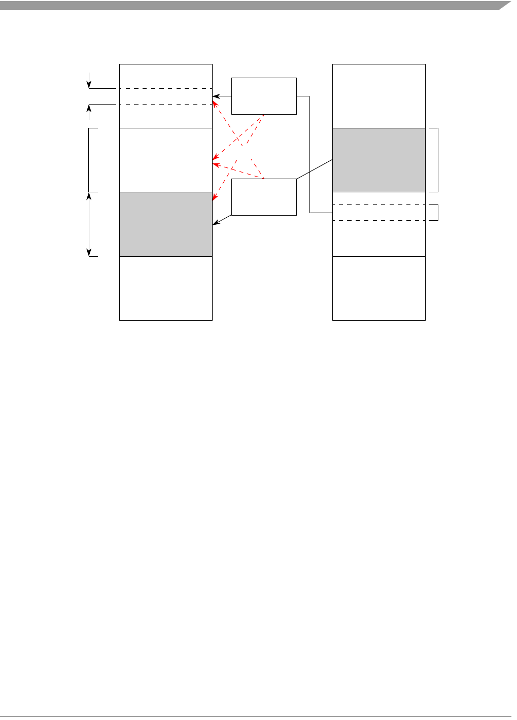
Application Information
MCF548x Reference Manual, Rev. 3
Freescale Semiconductor 19-73
Figure 19-54. Inbound Address Map
19.5.2.1.2 Outbound Address Translation
Figure 19-55 shows an example of XL Bus Initiator Window configurations. Overlapping the inbound
memory window (MCF548x Memory) and the outbound translation window is not supported and can
cause unpredictable behavior.
Figure 19-55 does not show the configuration mechanism.
0
4G
Register Space
PCI Space
3G
2G
1G
PCI Space (Memory View)MCF548x Space
0
4G
System Memory
MCF548x Memory
TBATR0
Address
Inbound
Translation
Base Address 0
MCF548X
BAR0
3G
2G
1G
Translation
SDRAM Space
TBATR1
Address
Translation MCF548x Memory
MCF548X
BAR1
Initiator
Windows
Inbound
Translation
Base Address 1
Not
Recommended
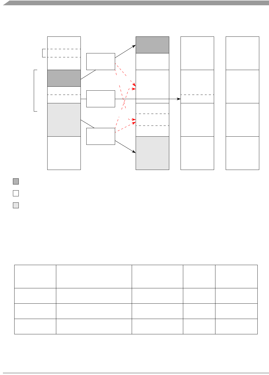
MCF548x Reference Manual, Rev. 3
19-74 Freescale Semiconductor
Figure 19-55. Outbound Address Map
19.5.2.1.3 Base Address Register Overview
Table 19-58 shows the available accessibility for all PCI associated base address and translation address
registers in the MCF548x.
Table 19-58. Address Register Accessibility
Base Address
Register Register Function
PCI Bus
Configuration
Access
Processor
Access
Any XL Bus
Master Access
BAR0 PCI Base Address Register 0
(256 Kbyte)
X X X
BAR1 PCI Base Address Register 1
(1 Gbyte)
X X X
TBATR0 Target Base Address Translation
Register 0 (256 Kbyte)
X X
0
4G
Register Space
3G
2G
1G
PCI Space
Window 2
XLB
Initiator
Windows
0
4G
3G
2G
1G
0
4G
3G
2G
1G
0
4G
3G
2G
1G
MCF548X
Window 2
Window 0
Window 0
Window 0
Translation
Window 1
MBAR
Window 1
Translation Window 1
Not Recommended
Window 2
Translation
Not Recommended
Window 2 Base Address = 0x80
Window 2 Address Mask = 0x3F
Window 2 Translation Address = 0xC0
Window 0 Base Address = 0x40
Window 0 Address Mask = 0x1F
Window 0 Translation Address = 0x00
Associated with PCI
Prefetchable Memory
Window 1 Base Address = 0x70
Window 1 Address Mask = 0x0F
Window 1 Translation Address = 0x70
Associated with PCI
Non-Prefetchable Memory
Associated with PCI I/O
(Memory View)
PCI Space
(I/O View)
(Configuration
View)
MCF548X
Memory
Memory
MCF548x Space

XL Bus Arbitration Priority
MCF548x Reference Manual, Rev. 3
Freescale Semiconductor 19-75
19.6 XL Bus Arbitration Priority
To prevent XL bus arbitration livelock, the PCI controller should have the same or higher XL bus
arbitration priority as other XL bus masters that access PCI space. If the XL bus arbiter master priority
register (PRI) is used, it should be programmed so that the PCI priority value has higher XL bus priority
than all other XL bus masters that address the PCI space through the XL bus slave interface of the PCI
Controller. XL bus masters that do not perform transactions to PCI across the XL internal bus can have
higher priority.
Note that the default priority setting uses the programmed priority settings where the G2 Core is set to
highest. If the Priority Register Enable is disabled for PCI (Master 3), the arbiter uses the hardware priority
values. The PCI hardwired priority is 0, highest. See Section 20.3, “Register Definition,” for more details.
TBATR1 Target Base Address Translation
Register 0 (1 Gbyte)
X X
IMWBAR Initiator Window Base/Translation
Address Registers
X X
Table 19-58. Address Register Accessibility (Continued)
Base Address
Register Register Function
PCI Bus
Configuration
Access
Processor
Access
Any XL Bus
Master Access

MCF548x Reference Manual, Rev. 3
19-76 Freescale Semiconductor
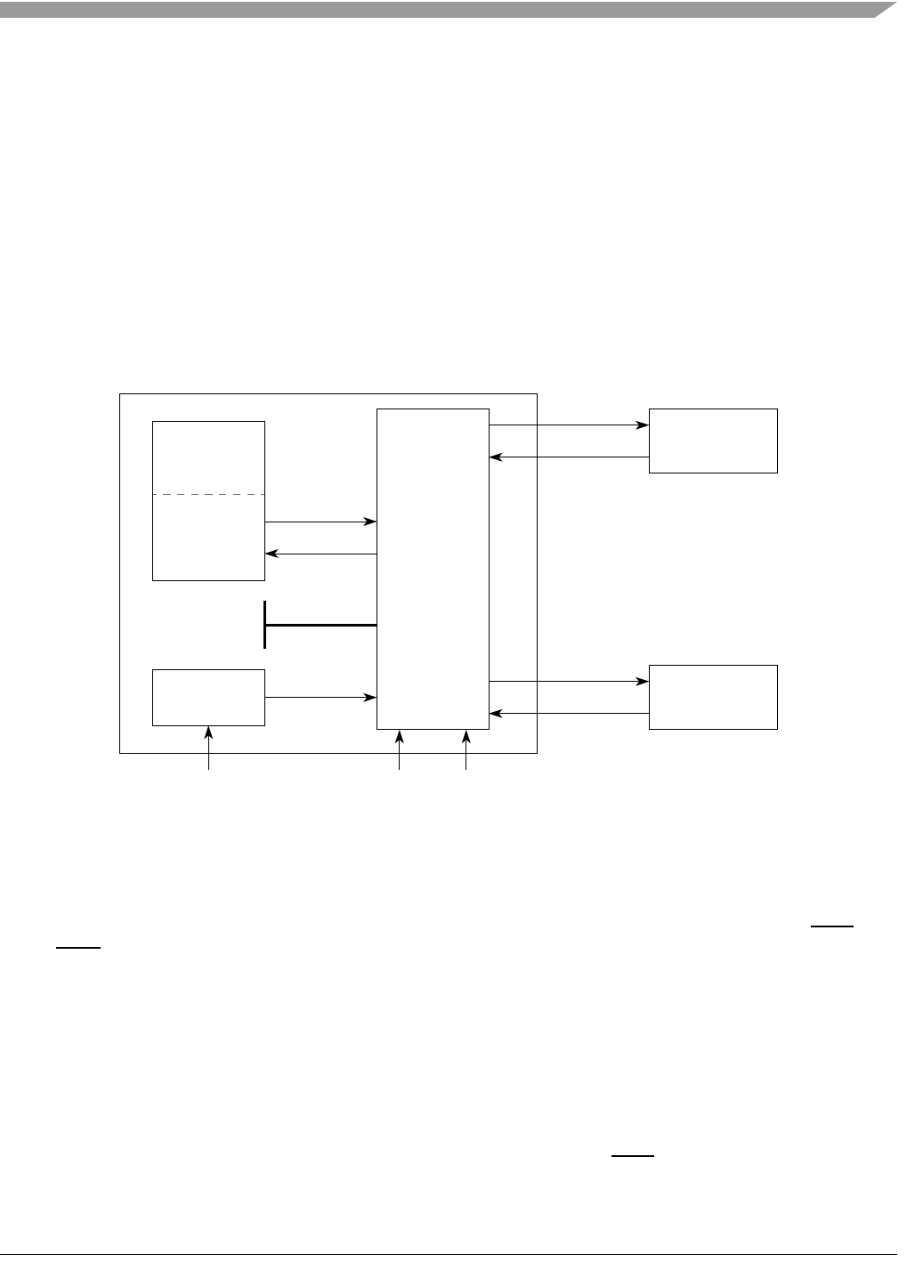
MCF548x Reference Manual, Rev. 3
Freescale Semiconductor 20-1
Chapter 20
PCI Bus Arbiter Module
20.1 Introduction
This chapter describes the MCF548x PCI bus arbiter module, including timing for request and grant
handshaking, the arbitration process, and the registers in the PCI bus arbiter programing model. It also
provides arbitration examples. For information on the PCI Controller, see Chapter 19, “PCI Bus
Controller.”
20.1.1 Block Diagram
Figure 20-1. PCI Arbiter Interface Diagram
20.1.2 Overview
PCI bus arbitration is access-based. Bus masters must arbitrate for each access performed on the bus. The
PCI bus uses a central arbitration scheme where each PCI master has its own unique request (REQ) and
grant (GNT) signal. A simple request-grant handshake is used to gain access to the bus.
The MCF548x contains an internal PCI bus arbiter that supports up to five external masters in addition to
the MCF548x. It can be disabled to allow for an external PCI arbiter.
The arbiter makes use of overlapped or “hidden” arbitration to reduce arbitration overhead and improve
bus utilization. Only during idle states of the PCI bus are cycles consumed due to arbitration.
When no device is using or requesting the PCI bus, the PCI arbiter parks the bus with the last master that
acquired the bus. The bus is then immediately available to the selected bus master if it should require the
use of the bus (and no other higher-priority request is pending). The selected master can immediately
initiate a transaction as long as the PCI bus is idle. It need not assert its REQ.
PCI Device 0
MCF548X PCI
Controller
Initiator
Interface
INT REQ
INT GNT
PCI Device 4
Clock Enable/
PLL
PCIBG4
PCIBR4
PCIBR0
PCIBG0
CLKIN
Slave
Bus
PCIIRDYPCIFRM
PCI
Arbiter
CLKIN
•
•
•
•
•
•
•
•
•
•
•
•
•
•
•
•
•
•
•
•
•
•
•
•
•
•
•
•
•
•
•
•
•
•
•
•

MCF548x Reference Manual, Rev. 3
20-2 Freescale Semiconductor
20.1.3 Features
• Direct support for up to five external PCI bus masters
• Fair arbitration scheme
• Hidden bus arbitration
• Bus parking
• Master time-out
• Interface with 33 MHz and 66 MHz PCI
20.2 External Signal Description
This section defines the PCI arbiter and corresponding external I/O signals. Table 20-1 summarizes this
information.
20.2.1 Frame (PCIFRM)
The PCIFRM signal is asserted by a PCI initiator to indicate the beginning of a transaction. It is deasserted
when the initiator is ready to complete the final data phase.
20.2.2 Initiator Ready (PCIIRDY)
The PCIIRDY signal is asserted to indicate that the PCI initiator is ready to transfer data. During a write
operation, assertion indicates that the master is driving valid data on the bus. During a read operation,
assertion indicates that the master is ready to accept data.
20.2.3 PCI Clock (CLKIN)
The CLKIN signal serves as a reference clock for generation of the internal PCI clock.
20.2.4 External Bus Grant (PCIBG[4:1])
The PCIBG signal is asserted to an external master to give it control of the PCI bus. If the internal PCI
arbiter is enabled, it asserts one of the PCIBG[4:1] lines to grant ownership of the PCI bus to an external
master. When the PCI arbiter module is disabled, PCIBG[4:1] are driven high and should be ignored.
Table 20-1. PCI Arbiter External Signals
Name Type Function MCF548x Reset
PCIFRM I/O Frame Tristate
PCIIRDY I/O Initiator Ready Tristate
CLKIN IClock Toggling
PCIBG0 / PCIREQOUT OExternal Bus Grant / Request Output Tristate
PCIBG[4:1] OExternal Bus Grant Tristate
PCIBR0 / PCIGNTIN IExternal Request / Grant Input Tristate
PCIBR[4:0] I External Bus Request Tristate

Register Definition
MCF548x Reference Manual, Rev. 3
Freescale Semiconductor 20-3
20.2.5 External Bus Grant/Request Output (PCIBG0/PCIREQOUT)
The PCIBG0 signal is asserted to external master device 0 to give it control of the PCI bus. When the PCI
arbiter module is disabled, the signal operates as the PCIREQOUT output. It is asserted when the
MCF548x needs to initiate a PCI transaction.
20.2.6 External Bus Request (PCIBR[4:1])
The PCIBR signal is asserted by an external PCI master when it requires access to the PCI bus.
20.2.7 External Request/Grant Input (PCIBR0/PCIGNTIN)
The PCIBR0 signal is asserted by external PCI master device 0 when it requires access to the PCI bus.
When the internal PCI arbiter module is disabled, this signal is used as a grant input for the PCI bus,
PCIGNTIN. It is driven by an external PCI arbiter.For detailed description of the PCI bus signals, see the
PCI Local Bus Specification, Revision 2.2.
20.3 Register Definition
The PCI arbiter provides decode logic for up to sixty-four 32-bit registers, but makes use of just two.
Accesses via the slave interface to and from the registers can be 8-bit, 16-bit, or 32-bit accesses. Reads to
unimplemented registers return 0x0000_0000 and writes have no effect.
All registers are accessible at an offset of MBAR in the memory space. There is one module offset for PCI
arbiter space at 0x0C00. Refer to for module offsets.
20.3.1 PCI Arbiter Control Register (PACR)
31 30 29 28 27 26 25 24 23 22 21 20 19 18 17 16
RDS000000000 EXTMINTEN INTMINTEN
W
Reset000000000000000 0
151413121110987654321 0
R0000000000 EXTMPRI INTMPRI
W
Reset000000000000000 0
Reg
Addr
MBAR + 0xC00
Figure 20-2. PCI Arbiter Control Register (PACR)

MCF548x Reference Manual, Rev. 3
20-4 Freescale Semiconductor
Table 20-2. PACR Field Descriptions
Bits Name Description
31 DS Disable bit for the internal PCI arbiter.
0 Enable the PCI arbiter.
1 Disable the on-chip arbiter and use GNT0 for the MCF548x PCI request output and REQ0 for
its grant input.
30–22 — Reserved, should be cleared.
21–17 EXTMINTEN External master broken interrupt enables. If an external master time-out occurs and the
corresponding interrupt enable bit is set, a CPU interrupt will be generated. Bit 21 is the enable
for PASR bit 21, bit 20 for PASR bit 20, and so on.
0 Disable interrupt
1 Enable interrupt
Software must write 1 to the asserted external master broken bit(s) in PASR to clear the
interrupt condition.
16 INTMINTEN Internal master broken interrupt enable for the MCF548x master time-out status bit internal
master broken (bit 16 of the PASR). If an MCF548x master time-out occurs and this bit is set,
a CPU interrupt will be generated.
0 Disable interrupt
1 Enable interrupt
Software must write 1 to the asserted internal master broken bit in PASR to clear the interrupt
condition.
15–6 — Reserved. Software should write zero to this register.
5–1 EXTMPRI External master priority levels. Bit 1 controls the priority for the device using REQ[0] and GNT0
pins, bit 2 for REQ1 and GNT1, etc.
0Low
1High
0 INTMPRI Internal master priority level.
0Low
1High

Functional Description
MCF548x Reference Manual, Rev. 3
Freescale Semiconductor 20-5
20.3.2 PCI Arbiter Status Register (PASR)
20.4 Functional Description
20.4.1 External PCI Requests
An external PCI master may target the MCF548x or external slaves. The request/grant handshake always
precedes any PCI bus operation. The PCI arbiter must service access requests for an external
master-to-external target transactions as well as external master-to-MCF548x transactions.
31 30 29 28 27 26 25 24 23 22 21 20 19 18 17 16
R0000000000 EXTMBK ITLMBK
Wrwc1rwc1
Reset000000000000000 0
151413121110987654321 0
R000000000000000 0
W
Reset000000000000000 0
Reg
Addr
MBAR + 0xC04
1Bits 21-16 are read-write-clear (rwc).
—Hardware can set rwc bits, but cannot clear them.
—Software can clear rwc bits that are currently set by writing a 1 to the bit location. Writing a 1 to a rwc bit
that is currently a 0 or writing a 0 to any rwc bit has no effect.
Figure 20-3. PCI Arbiter Status Register (PASR)
Table 20-3. PASR Field Descriptions
Bits Name Description
31–22 — Reserved. Software should write zero to this register.
21–17 EXTMBK External master broken: External master time-out. Bit 17 reports the time-out status for the device
using REQ0 and GNT0 pins, bit 18 for REQ1 and GNT1, etc. A CPU interrupt will be generated if
the corresponding external master interrupt enable bit is set. Software must write a 1 to each bit
location to clear.
16 ITLMBK Internal master broken: An MCF548xmaster time-out occurred. A CPU interrupt will be generated
if the internal master interrupt enable bit is set. Software must write a 1 to this bit location to clear.
15–0 — Reserved. Software should write zero to this register.

MCF548x Reference Manual, Rev. 3
20-6 Freescale Semiconductor
20.4.2 Arbitration
20.4.2.1 Hidden Bus Arbitration
PCI bus arbitration can take place while the currently granted device is performing a bus transaction if
another master is requesting access to the bus. As long as the bus is active, the arbiter can deassert GNT
to one master and assert GNT to the next in the same cycle and no PCI bus cycles are consumed due to
arbitration. The newly granted device must wait until the bus is relinquished by the current master before
initiating a transaction.
20.4.2.2 Arbitration Scheme
The MCF548x PCI bus master logic provides a programmable two-level least recently used (LRU) priority
algorithm. Two groups of masters are assigned, a high-priority group and a low-priority group. The
low-priority group as a whole represents one entry in the high-priority group. If the high-priority group
consists of n masters, then in at least every n+1 transactions, the highest priority is assigned to the
low-priority group. Low-priority masters have equal access to the bus with respect to other low-priority
masters. If there are masters programmed into both groups, masters in the high-priority group can be
serviced n transactions out of n+1, while one master in the low-priority group is serviced once every n+1
transactions. If all masters are programmed to the same group, or if there is only one master assigned to
the low-priority group, then there is no priority distinction among masters.
A LRU priority scheme allows for “fairness” in priority resolution because no one master can prevent other
masters from gaining access to the bus. The priority level, high or low, provides a simple weighting
mechanism for master access to the bus.
Priority in a LRU scheme adjusts so that the last master serviced is assigned the lowest priority in its level.
Masters with lower priority shift to the next higher priority position. The MCF548x is positioned before
all external devices in priority. If a master is not requesting the bus, its transaction slot is given to the next
requesting device within its priority group.
During hidden arbitration, GNT given to a requesting master while the PCI bus is active may be removed
and awarded to a higher priority device if a higher priority device asserts its request. If the bus is idle when
a device requests the bus, the arbiter deasserts the currently asserted GNT for one PCI clock cycle. The
arbiter evaluates the priorities of all requesting devices and grants the bus to the highest priority device in
the next cycle.
Figure 20-4 shows the initial state of the arbitration algorithm. Two devices are assigned high-priority (the
MCF548x and one external master) and four low-priority. If all masters request the use of the PCI bus
continuously, the GNT sequence is the MCF548x, device 1, device 0, the MCF548x, device 1, device 2,
the MCF548x, device 1, device 3, the MCF548x, device 1, device 4 repeating.
If device 1 is not requesting the bus, the GNT sequence is the MCF548x, device 0, the MCF548x, device
2, the MCF548x, device 3, the MCF548x, device 4 repeating. If, after this sequence completes, all devices
request the bus (including now device 1), the arbiter will assign GNT to device 1 since it has been the
longest since device 1 has used the bus. (It has highest priority.) Once all requests are serviced, the priority
resets to the initial state.

Functional Description
MCF548x Reference Manual, Rev. 3
Freescale Semiconductor 20-7
Figure 20-4. PCI Arbitration Initial State
20.4.2.3 Arbitration Latency
Worst case arbitration latency: arbitration latency is the number of clock cycles from a master’s REQ
assertion to PCI bus idle state AND its GNT assertion. In a lightly loaded system, arbitration latency would
be the time it takes for the bus arbiter to assert the master’s GNT (zero cycles if the arbiter is parked with
the requesting master and two if parked with another master). If a transaction is in progress when the
master’s GNT is asserted, the master must wait for the current transaction to complete and any subsequent
transactions from higher priority requesting masters. In a situation where there are multiple requesting
masters, each master’s tenure on the bus is limited by its master latency timer.
20.4.2.4 Arbitration Examples
Figure 20-5 shows basic arbitration. Three master devices are used to illustrate how an arbiter may
alternate bus accesses. (Assume device 0, device 1, and device 2 are assigned the same priority group and
no other masters are requesting use of the bus.)
High-Priority Group
MCF548X
(1/3)
Device 1
(1/3)
Low-Priority Group
Device 2
(1/12)
Low-Priority
Group Slot
(1/3) Device 4
(1/12)
Device 0
(1/12) Device 3
(1/12)
3a
1a2a
1b3b
4b
2b
PCI Arbiter Control Register PACR[26:31] = 000101b

MCF548x Reference Manual, Rev. 3
20-8 Freescale Semiconductor
Figure 20-5. Alternating Priority
Device 0 and device 1 assert REQ while the bus is parked with device 2. Because the PCI bus is idle, the
arbiter deasserts GNT to the parked master (device 2) and a cycle later, grants access to device 0. Device
0’s transaction begins when PCIFRAME is asserted on clock 4. (The earliest device 0 can initiate a
transaction on the PCI bus is the cycle following GNT assertion.) It leaves its REQ asserted to indicate it
wants to perform another transaction. When PCIFRAME is asserted (PCI bus is active), hidden arbitration
occurs and GNT to device 0 deasserts on the same cycle the arbiter asserts GNT to device 1. (Device 1 has
priority because, of the two requesting masters, device 0 and device 1, device 1 is the least recently used.)
Device 0 completes its transaction on clock 5 and relinquishes the PCI bus. On clock 6, device 1 detects
the PCI bus is idle (PCIFRAME and PCIIRDY deasserted) and because its GNT is still asserted, initiates
the next transaction in the next cycle. To indicate it only requires this single transaction on the PCI bus,
device 1 deasserts REQ on the same cycle it asserts PCIFRAME.
Because device 0 is the only other requesting device, the arbiter asserts its GNT and will leave its GNT
asserted until another request is detected.
Figure 20-6 starts out just like Figure 20-5 with the bus parked with device 2 and both device 0 and device
1 requesting use of the PCI bus. (Assume device 0, device 1, and device 2 are assigned the same priority
group and no other masters are requesting use of the bus.)
PCI_CLK
REQ[0]
REQ[1]
REQ[2]
GNT[0]
GNT[1]
PCIIRDY
PCIFRAME
PCIAD
0123456789101112
GNT[2]
DRIVEN LOW ADDR DATA ADDR DATA ADDR DATA
Access 0 Access 1 Access 0
STATE IDLE GRANT ACTIVE GRANT ACTIVE GRANT ACTIVETURN
(Parked)

Functional Description
MCF548x Reference Manual, Rev. 3
Freescale Semiconductor 20-9
Figure 20-6. Higher Priority Override
The arbiter again deasserts device 2’s GNT on clock 2, but device 2 initiates a transaction in the same
cycle. As long as the PCI bus is idle and GNT is asserted, a master can begin a transaction on the next
cycle. (Assertion of REQ is not required.)
Next access is again awarded to device 0 and upon detection of an idle PCI state, it performs its transaction
(clocks 5 and 6). Because it has subsequent transactions to perform, device 0 leaves its REQ asserted. Like
the previous timing diagram, PCI bus ownership switches to device 1.
While device 1 is performing a transaction on the PCI bus on clock 8, device 0 is the only device still
requesting subsequent use of the bus. In the next cycle, the arbiter asserts GNT to device 0 in response to
the request. Device 2, during that same cycle, asserts its REQ. The arbiter, because access 1 is still in
progress, determines that device 2 is higher priority than device 0 (after device 1 access), rearbitrates and
deasserts GNT to device 0 and asserts GNT to device 2 in the next cycle (clock 10).
20.4.3 Master Time-Out
A master is considered “broken” if it has not initiated an access (dropped PCIFRAME) after its GNT has
been asserted (its REQ is also asserted) and the bus is in the idle state for 16 clocks. A 16 clock (PCI clock)
timer is instituted to prevent arbitration lock-up for this case. When the timer expires, the arbiter removes
the GNT from the device and gives the bus to the master with the next highest priority. Subsequent requests
from the timed-out master will be ignored until its REQ is negated for at least one clock cycle.
A status bit is set when any master times out. If the corresponding interrupt enable bit is set, a CPU
interrupt will assert. Software can query the status bits to detect a “broken” master in the PCI system. (See
Section 20.3.2, “PCI Arbiter Status Register (PASR)”)
If a master does not initiate a transaction after its GNT has been asserted, but deasserts REQ before the 16
clock timer expires, the arbiter deasserts GNT and rearbitrates for the next transaction. The master is not
PCI_CLK
REQ[0]
REQ[1]
REQ[2]
GNT[0]
GNT[1]
PCIIRDY
PCIFRAME
PCIAD
0123456789101112
GNT[2]
LOW DATA ADDR DATA ADDR DATA
Access 2 Access 0
STATE IDLE ACTIVE GRANT ACTIVE GRANTTURN
(Parked)
ADDR
Access 1
ADDR DATA
Access 2
GRANTACTIVE ACTIVE

MCF548x Reference Manual, Rev. 3
20-10 Freescale Semiconductor
considered “broken” and subsequent requests are acknowledged. This “never-mind” scenario is
detrimental to system performance, however, and is not a recommended implementation.
20.5 Reset
Reset capability is provided by the MCF548x system reset. This signal resets both hardware and software
registers in the internal PCI arbiter.
An MCF548x software bit external to the arbiter controls the external PCIRESET signal (See
Section 19.3.2.1, “Global Status/Control Register (PCIGSCR)”). During the MCF548x system reset, this
bit is set and PCIRESET is asserted. No PCI traffic is allowed during this time. Only a software write of
zero brings the PCI bus out of reset.
Because the external PCI GNT signals must tristate during PCI reset, the PCIRESET output signal is used
as an output enable (active high) for all PCIGNT outputs.
20.6 Interrupts
Only a detection of a malfunctioning master can generate a CPU interrupt from the PCI arbiter module.
(see Section 20.4.3, “Master Time-Out”). If a master time-out occurs and its interrupt enable bit is set, a
level high will be driven onto the interrupt signal output of the arbiter. The interrupt will deassert when
either PASR[EXTMBK], the time-out status bit, or PASR[ITLMBK], the interrupt enable control bit, is
cleared.
When a master time-out occurs and the corresponding status bit is set, software must write a 1 to the bit
location to clear it. If the status bit generated an interrupt because the corresponding interrupt enable bit
was set, clearing the status bit is one way to deassert the interrupt output. An alternate way to force the
interrupt to a level low is to disable the interrupt enable that corresponds to the asserted status bit. The
status bit, however, remains set.
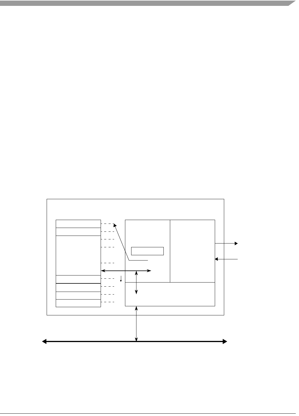
MCF548x Reference Manual, Rev. 3
Freescale Semiconductor 21-1
Chapter 21
FlexCAN
21.1 Introduction
The FlexCAN module is a communication controller implementing the controller area network (CAN)
protocol, an asynchronous communications protocol used in automotive and industrial control systems. It
is a high speed (1 Mbps), short distance, priority-based protocol that can communicate using a variety of
mediums (for example, fiber optic cable or an unshielded twisted pair of wires). The FlexCAN supports
both the standard and extended identifier (ID) message formats specified in the CAN protocol
specification, revision 2.0, part B.
The CAN protocol was primarily, but not only, designed to be used as a vehicle serial data bus, meeting
the specific requirements of this field: real-time processing, reliable operation in the EMI environment of
a vehicle, cost-effectiveness, and required bandwidth. A general working knowledge of the CAN protocol
revision 2.0 is assumed in this document. For details, refer to the CAN protocol revision 2.0 specification.
21.1.1 Block Diagram
A block diagram describing the various submodules of the FlexCAN module is shown in Figure 21-1.
Each submodule is described in detail in subsequent sections. The message buffer architecture is shown in
Figure 21-2.
Figure 21-1. FlexCAN Block Diagram and Pinout
MB15
MB14
•
•
MB3
MB2
MB1
MB0
Clocks, Address and Data Buses,
CAN
Protocol
Interface
Message
Buffer
Management CANTx
CANRx
Bus Interface Unit
Max MB #
[0:15]
IP-Bus Interface
Interrupt and Test Signals
FlexCAN
•
•
•
•
•
•
•
•
•
•
•
•
•
•
•
•
•
•
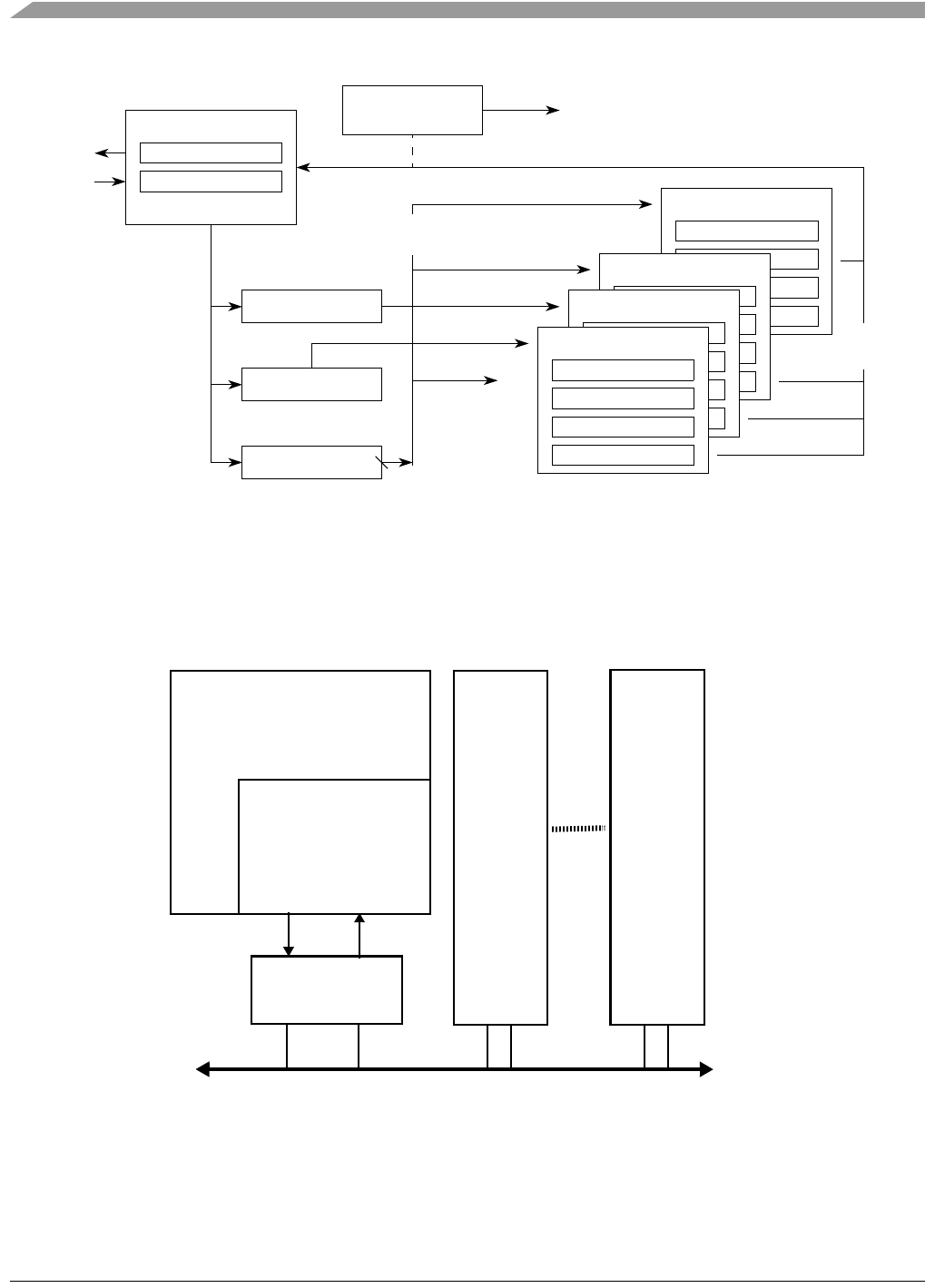
MCF548x Reference Manual, Rev. 3
21-2 Freescale Semiconductor
Figure 21-2. FlexCAN Message Buffer Architecture
21.1.2 The CAN System
A typical CAN system is shown below in Figure 21-3.
Figure 21-3. Typical CAN System
Each CAN station is connected physically to the CAN bus through a transceiver. The transceiver provides
the transmit drive, waveshaping, and receive/compare functions required for communicating on the CAN
ID
Data
Buffer 0
ID
Time Stamp
Data Length
Data
Buffer 13
ID
Time Stamp
Data Length
Data
Buffer 14
ID
Time Stamp
Data Length
Data
Buffer 15
•
•
•
•
•
•
•
•
Mask 15
Mask 14
Transparent to User
Rx Shifter
Tx Shifter
Serial Buffers
Tx
Rx
Control
Global Mask
IRQ or DMA Request
Data
•
•
•
•
•
•
16 Transmit/Receive
Message Buffers
CAN Bus
FlexCAN
CANRXn
Transceiver
CAN Station 1 CAN Station 2 CAN Station n
CANTXn
MCF548x

Introduction
MCF548x Reference Manual, Rev. 3
Freescale Semiconductor 21-3
bus. It can also provide protection against damage to the FlexCAN caused by a defective CAN bus or
defective stations.
21.1.3 Features
Following are the main features of the FlexCAN module:
• Full implementation of the CAN protocol specification version 2.0B
— Standard data and remote frames (up to 109 bits long)
— Extended data and remote frames (up to 127 bits long)
— 0–8 bytes data length
— Programmable bit rate up to 1 Mbps
— Content-related addressing
• Up to 16 flexible message buffers of 0–8 bytes data length, each configurable as Rx or Tx, all
supporting standard and extended messages
• Listen-only mode capability
• Three programmable mask registers: global (for MBs 0–13), special for MB14, and special for
MB15
• Programmable transmission priority scheme: lowest ID or lowest buffer number
• Time Stamp based on 16-bit free-running timer
• Global network time, synchronized by a specific message
• Programmable I/O modes
• Maskable interrupts
• Independent of the transmission medium (an external transceiver is assumed)
• Open network architecture
• Multimaster bus
• High immunity to EMI
• Short latency time due to an arbitration scheme for high-priority messages
21.1.4 Modes of Operation
21.1.4.1 Normal Mode
In normal mode, the module operates receiving and/or transmitting message frames, errors are handled
normally, and all the CAN protocol functions are enabled. User and supervisor modes differ in the access
to some restricted control registers.
21.1.4.2 Freeze Mode
Freeze mode is entered by:
• Setting CANMCR[FRZ], and
• Setting CANMCR[HALT], or by asserting the BKPT line.
Once entry into freeze mode is requested, the FlexCAN waits until an intermission or idle condition exists
on the CAN bus, or until the FlexCAN enters the error passive or bus off state. Once one of these
conditions exists, the FlexCAN waits for the completion of all internal activity like arbitration, matching,
move-in, and move-out. When this happens, the following events occur:
• The FlexCAN stops transmitting/receiving frames.

MCF548x Reference Manual, Rev. 3
21-4 Freescale Semiconductor
• The prescaler is disabled, thus halting all CAN bus communication.
• The FlexCAN ignores its Rx pins and drives its Tx pins as recessive.
• The FlexCAN loses synchronization with the CAN bus, and the NOTRDY and FRZACK bits in
CANMCR are set.
• The CPU is allowed to read and write the error counter registers (in other modes they are
read-only).
After engaging one of the mechanisms to place the FlexCAN in freeze mode, the user must wait for the
FRZACK bit to be set before accessing any other registers in the FlexCAN, otherwise unpredictable
operation may occur. In freeze mode, all memory mapped registers are accessible.
To exit freeze mode, the BKPT line must be negated or the HALT bit in CANMCR must be cleared. Once
freeze mode is exited, the FlexCAN will resynchronize with the CAN bus by waiting for 11 consecutive
recessive bits before beginning to participate in CAN bus communication.
21.1.4.3 Module Disabled Mode
This mode disables the FlexCAN module; it is entered by setting CANMCR[MDIS]. If the module is
disabled during freeze mode, it shuts down the system clocks, sets the LPMACK bit, and clears the
FRZACK bit.
If the module is disabled during transmission or reception, FlexCAN does the following:
• Waits to be in either idle or bus-off state, or else waits for the third bit of intermission and then
checks it to be recessive
• Waits for all internal activities like arbitration, matching, move-in, and move-out to finish
• Ignores its Rx input pin and drives its Tx pin as recessive
• Shuts down the system clocks
The bus interface unit continues to operate, enabling the CPU to access memory mapped registers, except
the free-running timer, the error counter register and the message buffers, which cannot be accessed when
the module is disabled. Exiting from this mode is done by negating the MDIS bit, which will resume the
clocks and negate the LPMACK bit.
21.1.4.4 Loop-Back Mode
The module enters this mode when the LPB bit in the control register is set. In this mode, FlexCAN
performs an internal loop back that can be used for self test operation. The bit stream output of the
transmitter is internally fed back to the receiver input. The Rx CAN input pin is ignored and the Tx CAN
output goes to the recessive state (logic 1). FlexCAN behaves as it normally does when transmitting and
treats its own transmitted message as a message received from a remote node. In this mode, FlexCAN
ignores the bit sent during the ACK slot in the CAN frame acknowledge field to ensure proper reception
of its own message. Both transmit and receive interrupts are generated.
21.1.4.5 Listen-Only Mode
In listen-only mode, the FlexCAN module is able to receive messages without giving an acknowledgment.
Whenever the module enters this mode, the status of the error counters is frozen and the FlexCAN module
operates like in error passive mode. Because the module does not influence the CAN bus in this mode, the
host device is capable of functioning like a monitor or for automatic bit-rate detection.

External Signals
MCF548x Reference Manual, Rev. 3
Freescale Semiconductor 21-5
21.2 External Signals
The FlexCAN module has two I/O signals connected to the external MPU pins: CANTX and CANRX.
Note that the general purpose I/O (GPIO) must be configured to enable the peripheral function of the
appropriate pins (refer to Chapter 15, “GPIO”) prior to configuring a FlexCAN channel.
21.2.1 CANTX[1:0]
CANTXn transmits serial data to the CAN bus transceiver.
21.2.2 CANRX[1:0]
CANRXn receives serial data from the CAN bus transceiver.
21.3 Memory Map/Register Definition
21.3.1 FlexCAN Memory Map
The FlexCAN module address space is split into 128 bytes starting at the base address, and then an extra
256 bytes starting at the base address +128. The upper 256 are fully used for the message buffer structures,
as described in Section 21.4.2, “Message Buffer Memory Map.” Out of the lower 128 bytes, only part is
occupied by various registers.
Table 21-1. FlexCAN Memory Map
MBAR Offset
Name Byte0 Byte1 Byte2 Byte3 Access
FlexCAN0 FlexCAN1
0xA000 0xA800 FlexCAN module
configuration register
CANMCR S
0xA004 0xA804 FlexCAN control register CANCTRL S/U
0xA008 0xA808 Timer register TIMER S/U
0xA00C 0xA80C Reserved —
0xA010 0xA8010 Rx global mask RXGMASK S/U
0xA014 0xA814 Rx buffer 14 mask RX14MASK S/U
0xA018 0xA818 Rx buffer 15 mask RX15MASK S/U
0xA01C 0xA81C Error counter register ERRCNT S/U
0xA020 0xA820 Error and status register ERRSTAT S/U
0xA024 0xA824 Reserved —
0xA028 0xA828 Interrupt mask register Reserved IMASK S/U
0xA02C 0xA82C Reserved —
0xA030 0xA830 Interrupt flag register Reserved IFLAG S/U

MCF548x Reference Manual, Rev. 3
21-6 Freescale Semiconductor
21.3.2 Register Descriptions
This section describes the registers in the FlexCAN module.
NOTE
The FlexCAN has no hard-wired protection against invalid bit/field
programming within its registers. Specifically, no protection is provided if
the programming does not meet CAN protocol requirements.
Programming the FlexCAN control registers is typically done during system initialization, prior to the
FlexCAN becoming synchronized with the CAN bus. The configuration registers can be changed after
synchronization by halting the FlexCAN module. This is done when the user sets the HALT bit in the
FlexCAN module configuration register (CANMCR). The FlexCAN responds by setting the
CANMCR[NOTRDY] bit. Additionally, the control registers can be modified while the MPU is in
background freeze mode.
21.3.2.1 FlexCAN Module Configuration Register (CANMCR)
CANMCR defines global system configurations, such as the module operation mode and maximum
message buffer configuration. Most of the fields in this register can be accessed at any time, except the
MAXMB field, which should only be changed while the module is in freeze mode.
0xA034–
0xA07F
0xA834–
0xA87F
Reserved —
0xA080–
0xA17F
0xA880–
0xA97F
Message buffers 0–15 MB S/U
31 30 29 28 27 26 25 24 23 22 21 20 19 18 17 16
R MDIS FRZ 0 HALT 0 0 SOFT
RST
FRZ
ACK
SUPV0000000
W
1101100010010000
15 14 13 12 11 10 9 8 7 6 5 4 3 2 1 0
R000000000000 MAXMB
W
Reset0000000000001111
Reg
Addr
MBAR + 0xA000 (CANMCR0); 0xA800 (CANMCR1)
Figure 21-4. FlexCAN Module Configuration Register (CANMCR)
Table 21-1. FlexCAN Memory Map (Continued)
MBAR Offset
Name Byte0 Byte1 Byte2 Byte3 Access
FlexCAN0 FlexCAN1

Memory Map/Register Definition
MCF548x Reference Manual, Rev. 3
Freescale Semiconductor 21-7
Table 21-2. CANMCR Field Descriptions
Bits Name Description
31 MDIS Module disable. This bit controls whether FlexCAN is enabled or not. When disabled, FlexCAN shuts
down the FlexCAN clocks. This is the only bit in CANMCR not affected by soft reset. See
Section 21.1.4.3, “Module Disabled Mode” for more information.
0 Enable the FlexCAN module, clocks enabled
1 Disable the FlexCAN module, clocks disabled
30 FRZ FREEZE assertion response. When FRZ = 1, the FlexCAN can enter debug mode when the BKPT
line is asserted or the HALT bit is set. Clearing this bit field causes the FlexCAN to exit debug mode.
Refer to Section 21.1.4.2, “Freeze Mode” for more information.
0 FlexCAN ignores the BKPT signal and the HALT bit in the module configuration register.
1 FlexCAN module enabled to enter debug mode.
29 — Reserved, should be cleared.
28 HALT Halt FlexCAN S-Clock. Setting the HALT bit has the same effect as assertion of the BKPT signal on
the FlexCAN without requiring that BKPT be asserted, i.e., it puts the FlexCAN module into freeze
mode. This bit is set to one after reset. It should be cleared after initializing the message buffers and
control registers. FlexCAN message buffer receive and transmit functions are inactive until this bit is
cleared. While in debug mode, the CPU has write access to the error counter register, that is
otherwise read-only.
When HALT is set, write access to certain registers and bits that are normally read-only is allowed.
0 The FlexCAN operates normally
1 FlexCAN enters debug mode if FRZ = 1
27–26 — Reserved, should be cleared.
25 SOFTRST Soft reset. When this bit is set, the FlexCAN resets its internal state machines (sequencer, error
counters, error flags, and timer) and the host interface registers (CANMCR [except the MDIS bit],
TIMER, ERRCNT, ERRSTAT, IMASK, and IFLAG).
The configuration registers that control the interface with the CAN bus are not changed (CANCTRL,
RXGMASK, RX14MASK, RX15MASK). Message buffers are also not changed. This allows
SOFTRST to be used as a debug feature while the system is running.
After setting SOFTRST, allow one complete bus cycle to elapse for the internal FlexCAN circuitry to
completely reset before executing another access to CANMCR.
The FlexCAN clears this bit once the internal reset cycle is completed.
0 Soft reset cycle completed
1 Soft reset cycle initiated
24 FRZACK FlexCAN disable. When the FlexCAN enters freeze mode, it sets the FRZACK bit. This bit should be
polled to determine if the FlexCAN has entered freeze mode. When freeze mode is exited, this bit is
negated once the FlexCAN prescaler is enabled. This is a read-only bit.
0 The FlexCAN has exited debug mode and the prescaler is enabled.
1 The FlexCAN has entered debug mode, and the prescaler is disabled.
23 SUPV Supervisor/user data space. The SUPV bit places the FlexCAN registers in either supervisor or user
data space.
0 Registers with access controlled by the SUPV bit are accessible in either user or supervisor
privilege mode.
1 Registers with access controlled by the SUPV bit are restricted to supervisor mode.

MCF548x Reference Manual, Rev. 3
21-8 Freescale Semiconductor
21.3.2.2 FlexCAN Control Register (CANCTRL)
CANCTRL is defined for specific FlexCAN control features related to the CAN bus, such as bit-rate,
programmable sampling point within an Rx bit, loop back mode, listen-only mode, bus off recovery
behavior, and interrupt enabling (for example, bus off, error). It also determines the division factor for the
clock prescaler. Most of the fields in this register should only be changed while the module is disabled or
in freeze mode. Exceptions are the BOFFMSK, ERRMSK, and BOFFREC bits, which can be accessed at
any time.
22–4 — Reserved, should be cleared.
3–0 MAXMB Maximum number of message buffers. This 6-bit field defines the maximum number of message
buffers that will take part in the matching and arbitration process. The reset value (0xF) is equivalent
to 16 message buffer (MB) configuration. This field should be changed only while the module is in
freeze mode.
31 30 29 28 27 26 25 24 23 22 21 20 19 18 17 16
RPRESDIV RJW PSEG1 PSEG2
W
Reset 0000000000 0 00000
15 14 13 12 11 10 9 8 7 6 5 4 3 2 1 0
RBOFF
MSK
ERR
MSK
0LPB0000SAMPBOFF
REC
TSYNC LBUF LOM PROPSEG
W
Reset 0000000000 0 00000
Reg
Addr
MBAR + 0xA004 (CANCTRL0); 0xA804 (CANCTRL1)
Figure 21-5. FlexCAN Control Register (CANCTRL)
Table 21-2. CANMCR Field Descriptions (Continued)
Bits Name Description
Maximum MBs in Use = MAXMB + 1

Memory Map/Register Definition
MCF548x Reference Manual, Rev. 3
Freescale Semiconductor 21-9
Table 21-3. CANCTRL Field Descriptions
Bits Name Description
31–24 PRESDIV Prescaler division factor. This 8-bit field defines the ratio between the system clock
frequency and the serial clock (S clock) frequency. The S clock period defines the time
quantum of the CAN protocol. For the reset value, the S clock frequency is equal to the
system clock frequency. The maximum value of this register is 0xFF, that gives a minimum
S clock frequency equal to the system clock frequency divided by 256. For more
information refer to Section 21.4.9, “Bit Timing.”
23–22 RJW Resyncronization jump width. This 2-bit field defines the maximum number of time quanta
(one time quantum is equal to the S clock period) that a bit time can be changed by one
resynchronization. The valid programmable values are 0–3.
21–19 PSEG1 Phase buffer segment 1. This 3-bit field defines the length of phase buffer segment 1 in the
bit time. The valid programmable values are 0–7.
18–16 PSEG2 Phase buffer segment 2. This 3-bit field defines the length of phase buffer segment 2 in the
bit time. The valid programmable values are 0–7.
15 BOFFMSK Bus off mask. This bit provides a mask for the bus off interrupt.
0 Bus off interrupt disabled
1 Bus off interrupt enabled
14 ERRMSK Error mask. This bit provides a mask for the error interrupt.
0 Error interrupt disabled
1 Error interrupt enabled
13 — Reserved, should be cleared.
12 LPB Loop back. This bit configures FlexCAN to operate in loop-back mode. In this mode,
FlexCAN performs an internal loop back that can be used for self test operation. The bit
stream output of the transmitter is fed back internally to the receiver input. The Rx CAN
input pin is ignored and the Tx CAN output goes to the recessive state (logic 1). FlexCAN
behaves as it normally does when transmitting, and treats its own transmitted message as
a message received from a remote node. In this mode, FlexCAN ignores the bit sent during
the ACK slot in the CAN frame acknowledge field, generating an internal acknowledge bit
to ensure proper reception of its own message. Both transmit and receive interrupts are
generated.
0 Loop back disabled
1 Loop back enabled
11–8 — Reserved, should be cleared.
7 SAMP Sampling mode. The SAMP bit determines whether the FlexCAN module will sample each
received bit one time or three times to determine its value.
0 One sample, taken at the end of phase buffer segment 1, is used to determine the value
of the received bit.
1 Three samples are used to determine the value of the received bit. The samples are
taken at the normal sample point and at the two preceding periods of the S-clock; a
majority rule is used.
S clock frequency f sys
PRESDIV + 1
------------------------------------=
Resync jump width = (RJW + 1) time quanta
Phase buffer segment 1 (PSEG1 + 1) time quanta=
Phase buffer segment 2 (PSEG2 + 1)time quanta =

MCF548x Reference Manual, Rev. 3
21-10 Freescale Semiconductor
21.3.2.3 FlexCAN Timer Register (TIMER)
This register represents a 16-bit free running counter that can be read and written to by the CPU. The timer
starts from 0x0000 after reset, counts linearly to 0xFFFF, and wraps around.
The timer is clocked by the FlexCAN bit-clock (which defines the baud rate on the CAN bus). During a
message transmission/reception, it increments by one for each bit that is received or transmitted. When
there is no message on the bus, it counts using the previously programmed baud rate. During freeze mode,
the timer is not incremented.
6 BOFFREC Bus off recovery mode. This bit defines how FlexCAN recovers from bus off state. If this bit
is cleared, automatic recovering from bus off state occurs according to the CAN
Specification 2.0B. If the bit is set, automatic recovering from bus off is disabled and the
module remains in bus off state until the bit is cleared by the user. If the bit is cleared before
128 sequences of 11 recessive bits are detected on the CAN bus, then bus off recovery
happens as if the BOFFREC bit had never been set. If the bit is cleared after 128
sequences of 11 recessive bits occurred, then FlexCAN will re-synchronize to the bus by
waiting for 11 recessive bits before joining the bus. After negation, the BOFFREC bit can
be set again during bus off, but it will only be effective the next time the module enters bus
off. If BOFFREC was cleared when the module entered bus off, setting it during bus off will
not be effective for the current bus off recovery.
0 Automatic recovering from bus off-state enabled, according to CAN Spec 2.0 part B
1 Automatic recovering from bus off state disabled
5 TSYNC Timer synchronize mode. The TSYNC bit enables the mechanism that resets the
free-running timer each time a message is received in Message Buffer 0. This feature
provides the means to synchronize multiple FlexCAN stations with a special “SYNC”
message (global network time).
0 Timer synchronization disabled.
1 Timer synchronization enabled.
Note: There can be a bit clock skew of four to five counts between different FlexCAN
modules that are using this feature on the same network.
4 LBUF Lowest buffer transmitted first. This bit defines the ordering mechanism for message buffer
transmission.
0 Message buffer with lowest ID is transmitted first
1 Lowest numbered buffer is transmitted first
3 LOM Listen-only mode. This bit configures FlexCAN to operate in listen-only mode. In this mode,
transmission is disabled, all error counters are frozen and the module operates in a CAN
error passive mode [Ref. 1]. Only messages acknowledged by another CAN station will be
received. If FlexCAN detects a message that has not been acknowledged, it will flag a BIT0
error (without changing the REC), as if it was trying to acknowledge the message.
0 FlexCAN module is in normal active operation, listen-only mode is deactivated
1 FlexCAN module is in listen-only mode operation
2–0 PROPSEG Propagation segment. This 3-bit field defines the length of the propagation segment in the
bit time. The valid programmable values are 0–7.
Note: A time-quantum = 1 serial clock S clock period.
Table 21-3. CANCTRL Field Descriptions (Continued)
Bits Name Description
Propagation segment time (PROPSEG + 1) time-quanta=

Memory Map/Register Definition
MCF548x Reference Manual, Rev. 3
Freescale Semiconductor 21-11
The timer value is captured at the beginning of the identifier (ID) field of any frame on the CAN bus. This
captured value is written into the TIMESTAMP entry in a message buffer after a successful reception or
transmission of a message.
Writing to the timer is an indirect operation. The data is first written to an auxiliary register, then an internal
request/acknowledge procedure across clock domains is executed. All this is transparent to the user, except
for the fact that the data will take some time to be actually written to the register. If desired, software can
poll the register to discover when the data was actually written.
Reg
21.3.2.4 Rx Mask Registers
These registers are used as acceptance masks for received frame IDs. Three masks are defined: a global
mask, used for Rx buffers 0–13 and 16–63, and two more separate masks for buffers 14 and 15. The
meaning of each mask is the following:
Mask bit = 0: The corresponding incoming ID bit is “don’t care”.
Mask bit = 1: The corresponding ID bit is checked against the incoming ID bit, to see if a match
exists.
Note that these masks are used both for Standard and Extended ID formats. The value of mask registers
should not be changed while in normal operation, as locked frames that matched a message buffer (MB)
through a mask may be transferred into the MB (upon release) but may no longer match.
31 30 29 28 27 26 25 24 23 22 21 20 19 18 17 16
R0000000000000000
W
Reset0000000000000000
1514131211109876543210
RTIMER
W
Reset0000000000000000
Reg
Addr
MBAR + 0xA008 (TIMER0); 0xA808 (TIMER1)
Figure 21-6. FlexCAN Timer Register (TIMER)
Table 21-4. Mask Examples for Normal/Extended Messages
Base ID
ID28.................ID18 IDE Extended ID
ID17......................................ID0 Match
MB2-ID 1 1 1 1 1 1 1 1 0 0 0 0
MB3-ID 1 1 1 1 1 1 1 1 0 0 0 1 0 1 0 1 0 1 0 1 0 1 0 1 0 1 0 1 0 1
MB4-ID 0 0 0 0 0 0 1 1 1 1 1 0
MB5-ID 0 0 0 0 0 0 1 1 1 0 1 1 0 1 0 1 0 1 0 1 0 1 0 1 0 1 0 1 0 1
MB14-ID 1 1 1 1 1 1 1 1 0 0 0 1 0 1 0 1 0 1 0 1 0 1 0 1 0 1 0 1 0 1
Rx_Global_Mask 1 1 1 1 1 1 1 1 1 1 0 1 1 1 1 1 1 1 0 0 0 0 0 0 0 0 0 0 1
Rx_Msg in11 1 1 1 1 1 1 1 0 0 1 1 0 1 0 1 0 1 0 1 0 1 0 1 0 1 0 1 0 1 31

MCF548x Reference Manual, Rev. 3
21-12 Freescale Semiconductor
21.3.2.4.1 FlexCAN Rx Global Mask Register (RXGMASK)
The Rx global mask bits are applied to all Rx identifiers, excluding Rx buffers 14–15 that have their
specific Rx mask registers. Access to this register is unrestricted.
Rx_Msg in21 1 1 1 1 1 1 1 0 0 1 0 22
Rx_Msg in31 1 1 1 1 1 1 1 0 0 1 1 0 1 0 1 0 1 0 1 0 1 0 1 0 1 0 1 0 0 3
Rx_Msg in40 1 1 1 1 1 1 1 0 0 0 0 4
Rx_Msg in50 1 1 1 1 1 1 1 0 0 0 1 0 1 0 1 0 1 0 1 0 1 0 1 0 1 0 1 0 1 145
RX14MASK 0 1 1 1 1 1 1 1 1 1 1 1 1 1 1 1 1 1 0 0 0 0 0 0 0 0 0 0 0
Rx_Msg in61 0 1 1 1 1 1 1 0 0 0 1 0 1 0 1 0 1 0 1 0 1 0 1 0 1 0 1 0 1 6
Rx_Msg in70 1 1 1 1 1 1 1 0 0 0 1 0 1 0 1 0 1 0 1 0 1 0 1 0 1 0 1 0 1 147
1Match for Extended Format (MB3).
2Match for Normal Format. (MB2).
3Mismatch for MB3 because of ID0.
4Mismatch for MB2 because of ID28.
5Mismatch for MB3 because of ID28, Match for MB14 (Uses RX14MASK).
6Mismatch for MB14 because of ID27 (Uses RX14MASK).
7Match for MB14 (Uses RX14MASK).
31 30 29 28 27 26 25 24 23 22 21 20 19 18 17 16
R 0 0 0 MI28 MI27 MI26 MI25 MI24 MI23 MI22 MI21 MI20 MI19 MI18 MI17 MI16
W
Reset0001111111111111
1514131211109876543210
R MI15 MI14 MI13 MI12 MI11 MI10 MI9 MI8 MI7 MI6 MI5 MI4 MI3 MI2 MI1 MI0
W
Reset1111111111111111
Reg
Addr
MBAR + 0xA010 (RXGMASK0); 0xA810 (RXGMASK1)
Figure 21-7. FlexCAN Rx Global Mask Register (RXGMASK)
Table 21-5. RXGMASK Field Descriptions
Bits Name Description
31–29 — Reserved, should be cleared.
Table 21-4. Mask Examples for Normal/Extended Messages (Continued)
Base ID
ID28.................ID18 IDE Extended ID
ID17......................................ID0 Match

Memory Map/Register Definition
MCF548x Reference Manual, Rev. 3
Freescale Semiconductor 21-13
21.3.2.4.2 FlexCAN Rx 14 Mask Register (RX14MASK)
The RX14MASK register has the same structure as the Rx global mask register and is used to mask
message buffer 14. Access to this register is unrestricted.
21.3.2.4.3 FlexCAN Rx 15 Mask Register (RX15MASK)
The RX15MASK register has the same structure as the Rx global mask register and is used to mask
message buffer 15. Access to this register is unrestricted.
28–18 MI28–MI18 Standard ID mask bits. These bits are the same mask bits for the Standard and Extended
Formats.
17–0 MI17–MI0 Extended ID mask bits. These bits are used to mask comparison only in Extended Format.
31 30 29 28 27 26 25 24 23 22 21 20 19 18 17 16
R 0 0 0 MI28 MI27 MI26 MI25 MI24 MI23 MI22 MI21 MI20 MI19 MI18 MI17 MI16
W
Reset0001111111111111
1514131211109876543210
R MI15 MI14 MI13 MI12 MI11 MI10 MI9 MI8 MI7 MI6 MI5 MI4 MI3 MI2 MI1 MI0
W
Reset1111111111111111
Reg
Addr
MBAR + 0xA014 (RX14MASK0); (0xA814 (RX14MASK1)
Figure 21-8. FlexCAN Rx14 Mask Register
Table 21-6. RX14MASK Field Descriptions
Bits Name Description
31–29 — Reserved, should be cleared.
28–18 MI28–MI18 Standard ID mask bits. These bits are the same mask bits for the Standard and Extended
Formats.
17–0 MI17–MI0 Extended ID mask bits. These bits are used to mask comparison only in Extended Format.
Table 21-5. RXGMASK Field Descriptions (Continued)
Bits Name Description

MCF548x Reference Manual, Rev. 3
21-14 Freescale Semiconductor
21.3.2.5 FlexCAN Error Counter Register (ERRCNT)
This register has two 8-bit fields reflecting the value of two FlexCAN error counters: transmit error counter
(TXECTR) and receive error counter (RXECTR). The rules for increasing and decreasing these counters
are described in the CAN protocol and are completely implemented in the FlexCAN module. Both
counters are read-only except in freeze mode, where they can be written by the CPU.
Writing to the error counter register while in freeze mode is an indirect operation. The data is first written
to an auxiliary register and then an internal request/acknowledge procedure across clock domains is
executed. All this is transparent to the user, except for the fact that the data will take some time to be
actually written to the register. If desired, software can poll the register to discover when the data was
actually written.
FlexCAN responds to any bus state as described in the protocol, e.g. transmit error-active or error-passive
flag, delay its transmission start time (error-passive), and avoid any influence on the bus when in bus off
state. The following are the basic rules for FlexCAN bus state transitions:
• If the value of TXECTR or RXECTR increases to be greater than or equal to 128, the FLTCONF
field in the error and status register is updated to reflect error-passive state.
• If the FlexCAN state is error-passive, and either TXECTR or RXECTR decrements to a value less
than or equal to 127 while the other already satisfies this condition, the FLTCONF field in the error
and status register is updated to reflect error-active state.
• If the value of TXECTR increases to be greater than 255, the FLTCONF field in the error and status
register is updated to reflect bus off state, and an interrupt may be issued. The value of TXECTR
is then reset to zero.
• If FlexCAN is in bus off state, then TXECTR is cascaded together with another internal counter to
count the 128th occurrences of 11 consecutive recessive bits on the bus. Hence, TXECTR is reset
31 30 29 28 27 26 25 24 23 22 21 20 19 18 17 16
R 0 0 0 MI28 MI27 MI26 MI25 MI24 MI23 MI22 MI21 MI20 MI19 MI18 MI17 MI16
W
Reset0001111111111111
1514131211109876543210
R MI15 MI14 MI13 MI12 MI11 MI10 MI9 MI8 MI7 MI6 MI5 MI4 MI3 MI2 MI1 MI0
W
Reset1111111111111111
Reg
Addr
MBAR + 0xA018 (RX15MASK0); 0xA818 (RX15MASK1)
Figure 21-9. FlexCAN Rx15 Mask Register (RX15MASK)
Table 21-7. RX15MASK Field Descriptions
Bits Name Description
31–29 — Reserved, should be cleared.
28–18 MI28–MI18 Standard ID mask bits. These bits are the same mask bits for the Standard and Extended
Formats.
17–0 MI17–MI0 Extended ID mask bits. These bits are used to mask comparison only in Extended Format.

Memory Map/Register Definition
MCF548x Reference Manual, Rev. 3
Freescale Semiconductor 21-15
to zero and counts in a manner where the internal counter counts 11 such bits, then wraps around
while incrementing the TXECTR. When TXECTR reaches the value of 128, the FLTCONF field
in the error and status register is updated to be error-active, and both error counters are reset to zero.
At any instance of dominant bit following a stream of less than 11 consecutive recessive bits, the
internal counter resets itself to zero without affecting the TXECTR value.
• If during system start-up, only one node is operating, then its TXECTR increases in each message
it is trying to transmit, as a result of acknowledge errors (indicated by the ACKERR bit in the error
and status register). After the transition to error-passive state, the TXECTR does not increment
anymore by acknowledge errors. Therefore the device never goes to the bus off state.
• If the RXECTR increases to a value greater than 127, it is not incremented further, even if more
errors are detected while being a receiver. At the next successful message reception, the counter is
set to a value between 119 and 127 to resume to error-active state.
21.3.2.6 FlexCAN Error and Status Register (ERRSTAT)
ERRSTAT reflects various error conditions, some general status of the device, and is the source of three
interrupts to the host. The reported error conditions (bits 15:10) are those occurred since the last time the
host read this register. The read action clears bits 15-10. Bits 9–3 are status bits.
Most bits in this register are read only, except for BOFFINT, WAKINT, and ERRINT, which are interrupt
sources that can be cleared by writing 1 to them. Writing 0 has no effect. Refer to Section 21.5.1,
“Interrupts.”
31 30 29 28 27 26 25 24 23 22 21 20 19 18 17 16
R0000000000000000
W
Reset0000000000000000
1514131211109876543210
R RXECTR TXECTR
W
Reset0000000000000000
Reg
Addr
MBAR + 0xA01C (ERRCNT0); 0xA81C (ERRCNT1)
Figure 21-10. FlexCAN Error Counter Register (ERRCNT)

MCF548x Reference Manual, Rev. 3
21-16 Freescale Semiconductor
Table 21-8 describes the ERRSTAT fields.
31 30 29 28 27 26 25 24 23 22 21 20 19 18 17 16
R0000000000000000
W
Reset0000000000000000
1514131211109876543210
RBITERR ACK
ERR
CRC
ERR
FRM
ERR
STF
ERR
TX
WRN
RX
WRN
IDLE TXRX FLT
CONF
0BOFF
INT
ERR
INT
0
W
Reset0000000000000000
Reg
Addr
MBAR + 0xA020 (ERRSTAT0); 0xA820 (ERRSTAT1)
Figure 21-11. FlexCAN Error and Status Register (ERRSTAT)
Table 21-8. ERRSTAT Field Descriptions
Bits Name Description
31–16 — Reserved, should be cleared.
15–14 BITERR Transmit bit error. The BITERR[1:0] field is used to indicate when a transmit bit error occurs.
00 No transmit bit error
01 At least one bit sent as dominant was received as recessive
10 At least one bit sent as recessive was received as dominant
11 Reserved
Note: The transmit bit error field is not modified during the arbitration field or the ACK slot bit time
of a message, or by a transmitter that detects dominant bits while sending a passive error frame.
13 ACKERR Acknowledge error. The ACKERR bit indicates whether an acknowledgment has been correctly
received for a transmitted message.
0 No ACK error was detected since the last read of this register.
1 An ACK error was detected since the last read of this register.
12 CRCERR Cyclic redundancy check error. The CRCERR bit indicates whether or not the CRC of the last
transmitted or received message was valid.
0 No CRC error was detected since the last read of this register.
1 A CRC error was detected since the last read of this register.
11 FRMERR Message format error. The FORMERR bit indicates whether or not the message format of the last
transmitted or received message was correct.
0 No format error was detected since the last read of this register.
1 A format error was detected since the last read of this register.
10 STFERR Bit stuff error. The STUFFERR bit indicates whether or not the bit stuffing that occurred in the last
transmitted or received message was correct.
0 No bit stuffing error was detected since the last read of this register.
1 A bit stuffing error was detected since the last read of this register.
9 TXWRN Transmit error status flag. The TXWARN status flag reflects the status of the FlexCAN transmit error
counter.
0 Transmit error counter < 96
1 TXErrCounter ≥ 96

Memory Map/Register Definition
MCF548x Reference Manual, Rev. 3
Freescale Semiconductor 21-17
21.3.2.7 Interrupt Mask Register (IMASK)
IMASK contains one interrupt mask bit per buffer. It enables the CPU to determine which buffer will
generate an interrupt after a successful transmission/reception (that is, when the corresponding IFLAG bit
is set).
The interrupt mask register contains two 8-bit fields: bits 15-8 (IMASK_H) and bits 7-0 (IMASK_L). The
register can be accessed by the master as a 16-bit register, or each byte can be accessed individually using
an 8-bit (byte) access cycle.
8 RXWRN Receiver error status flag. The RXWARN status flag reflects the status of the FlexCAN receive error
counter.
0 Receive error counter < 96
1 RxErrCounter ≥ 96
7 IDLE Idle status. The IDLE bit indicates when there is activity on the CAN bus.
0 The CAN bus is not idle.
1 The CAN bus is idle.
6 TXRX Transmit/receive status. The TX/RX bit indicates when the FlexCAN module is transmitting or
receiving a message. TX/RX has no meaning when IDLE = 1.
0 The FlexCAN is receiving a message if IDLE = 0.
1 The FlexCAN is transmitting a message if IDLE = 0.
5–4 FLTCONF Fault confinement state. This 2-bit field indicates the confinement state of the FlexCAN module, as
shown below. If the LOM bit in the control register is asserted, the FLTCONF field will indicate
error-passive. Since the control register is not affected by soft reset, the FLTCONF field will not be
affected by soft reset if the LOM bit is asserted.
00 Error active
01 Error passive
1x Bus off
3 — Reserved, should be cleared.
2 BOFFINT Bus off interrupt. The BOFFINT bit is used to request an interrupt when the FlexCAN enters the bus
off state.
0 No bus off interrupt requested.
1 When the FlexCAN state changes to bus off, this bit is set, and if the BOFFMSK bit in CANCTRL
is set, an interrupt request is generated. This interrupt is not requested after reset.
1 ERRINT Error interrupt. The ERRINT bit is used to request an interrupt when the FlexCAN detects a transmit
or receive error.
0 No error interrupt request.
1 If an event which causes one of the error bits in the error and status register to be set occurs, the
error interrupt bit is set. If the ERRMSK bit in CANCTRL is set, an interrupt request is generated.
To clear this bit, first read it as a one, then write as a zero. Writing a one has no effect.
0—Reserved, should be cleared.
Table 21-8. ERRSTAT Field Descriptions (Continued)
Bits Name Description

MCF548x Reference Manual, Rev. 3
21-18 Freescale Semiconductor
Table 21-10 describes the IMASK fields.
21.3.2.8 Interrupt Flag Register (IFLAG)
IFLAG contains one interrupt flag bit per buffer. Each successful transmission/reception sets the
corresponding IFLAG bit and, if the corresponding IMASK bit is set, will generate an interrupt.
The interrupt flag is cleared by writing a 1. Writing 0 has no effect.
This register contains two 8-bit fields: bits 15–8 (IFLAG_H) and bits 7–0 (IFLAG_L). The register can be
accessed by the master as a 16-bit register, or each byte can be accessed individually using an 8-bit (byte)
access cycle.
Table 21-12 describes the IFLAG fields.
1514131211109876543210
IMASK_H IMASK_L
RBUF
15M
BUF
14M
BUF
13M
BUF
12M
BUF
11M
BUF
10M
BUF
9M
BUF
8M
BUF7
M
BUF
6M
BUF
5M
BUF
4M
BUF
3M
BUF
2M
BUF
1M
BUF
0M
W
Reset0000000000000000
Reg
Addr
MBAR + 0xA02A (IMASK0); 0xA82A (IMASK1)
Table 21-9. FlexCAN Interrupt Mask Register (IMASK)
Table 21-10. IMASK Field Descriptions
Bits Name Description
15–0 BUFnM IMASK contains one interrupt mask bit per buffer. It allows the CPU to designate which buffers will
generate interrupts after successful transmission/reception. Each bit enables or disables the
respective FlexCAN message buffer (MB0 to MB15) interrupt.
0 The interrupt for the corresponding buffer is disabled.
1 The interrupt for the corresponding buffer is enabled.
Note: Setting or clearing an IMASK bit can assert or negate an interrupt request, if the
corresponding IFLAG bit it is set.
151141391211109876543210
IFLAG_H IFLAG_L
RBUF
15I
BUF
14I
BUF
13I
BUF
12I
BUF
11I
BUF
10I
BUF
9I
BUF
8I
BUF7
I
BUF
6I
BUF
5I
BUF
4I
BUF
3I
BUF
2I
BUF
1I
BUF
0I
W
Reset0000000000000000
Reg
Addr
MBAR + 0xA032 (IFLAG0); 0xA832 (IFLAG1)
Table 21-11. FlexCAN Interrupt Flags Register (IFLAG)

Functional Overview
MCF548x Reference Manual, Rev. 3
Freescale Semiconductor 21-19
21.4 Functional Overview
The FlexCAN module is flexible in that each one of its 16 message buffers (MBs) can be assigned either
as a transmit buffer or a receive buffer. Each MB, which is up to 8 bytes long, is also assigned an interrupt
flag bit that indicates successful completion of either transmission or reception.
An arbitration algorithm decides the prioritization of MBs to be transmitted based on either the message
ID or the MB ordering. A matching algorithm makes it possible to store received frames only into MBs
that have the same ID programmed on its ID field. A masking scheme makes it possible to match the ID
programmed on the MB with a range of IDs on received CAN frames. A reception queue can be
implemented by programming the same ID on more than one receiving MB. Data coherency mechanisms
are implemented to guarantee data integrity during MB manipulation by the CPU.
Before proceeding with the functional description, an important concept must be explained. A message
buffer is said to be “active” at a given time if it can participate in the matching and arbitration algorithms
that are happening at that time. An Rx MB with a 0b0000 code is inactive (refer to Table 21-14). Similarly,
a Tx MB with a 0b1000 code is inactive (refer to Table 21-15). A MB not programmed with either 0b0000
or 0b1000 will be temporarily deactivated (will not participate in the current arbitration/matching run)
when the CPU writes to the C/S field of that MB.
NOTE
For both the transmit and the receive processes, the first CPU action in
preparing a MB should be to deactivate it by setting its CODE field to the
proper value. This requirement is mandatory to assure proper operation.
21.4.1 Message Buffer Structure
The message buffer structure used by the FlexCAN module is defined in the CAN Specification Version
2.0, Part B and is represented in Figure 21-12. The specification includes both standard and extended
frames. A standard frame is represented by the 11-bit standard identifier, and an extended frame is
represented by the combined 29-bits of the standard identifier (11 bits) and the extended identifier (18
bits).
Table 21-12. IFLAG Field Descriptions
Bits Name Description
15–0 BUFnI IFLAG contains one interrupt flag bit per buffer. Each successful transmission/reception sets the
corresponding IFLAG bit and, if the corresponding IMASK bit is set, an interrupt request will be
generated.
To clear an interrupt flag, first read the flag as a one, and then write it as a one. Should a new flag
setting event occur between the time that the CPU reads the flag as a one and writes the flag as a
one, the flag is not cleared.
0 No such occurence.
1 The corresponding buffer has successfully completed transmission or reception.

MCF548x Reference Manual, Rev. 3
21-20 Freescale Semiconductor
313029282726252423 22 21 20 191817161514131211109876543210
0x0 CODE SRR IDE RTR LENGTH TIME STAMP
0x4 Standard ID [28:18] Extended ID [17:0]
0x8 Data Byte 0 Data Byte 1 Data Byte 2 Data Byte 3
0xC Data Byte 4 Data Byte 5 Data Byte 6 Data Byte 7
Figure 21-12. Message Buffer Structure for Both Extended and Standard Frames
Table 21-13. Message Buffer Field Descriptions
Bits Name Description
31–28 — Reserved, should be cleared. Should not be accessed by the CPU.
27–24 CODE Message buffer code. This 4-bit field can be accessed (read or write) by the CPU and by the
FlexCAN module itself, as part of the message buffer matching and arbitration process. The
encoding is shown in Table 2 1- 14 and Table 21-15. See Section 21.4, “Functional Overview” for
additional information.
23 — Reserved, should be cleared. Should not be accessed by the CPU.
22 SRR Substitute remote request. Fixed recessive bit, used only in extended format. It must be set to 1 by
the user for transmission (Tx Buffers) and will be stored with the value received on the CAN bus
for Rx receiving buffers. It can be received as either recessive or dominant. If FlexCAN receives
this bit as dominant, then it is interpreted as arbitration loss.
0 Dominant is not a valid value for transmission in Extended Format frames
1 Recessive value is compulsory for transmission in Extended Format frames
21 IDE ID extended bit. This bit identifies whether the frame format is standard or extended.
0 Frame format is standard
1 Frame format is extended
20 RTR Remote transmission request. This bit is used for requesting transmissions of a data frame. If
FlexCAN transmits this bit as 1 (recessive) and receives it as 0 (dominant), it is interpreted as
arbitration loss. If this bit is transmitted as 0 (dominant), then if it is received as 1 (recessive), the
FlexCAN module treats it as bit error. If the value received matches the value transmitted, it is
considered as a successful bit transmission.
0 Indicates the current MB has a data frame to be transmitted
1 Indicates the current MB has a remote frame to be transmitted
19–16 LENGTH Length of data in bytes. This 4-bit field is the length (in bytes) of the Rx or Tx data; data is located
in offset 0x8 through 0xF of the MB space (see Figure 21-12). In reception, this field is written by
the FlexCAN module, copied from the DLC (data length code) field of the received frame. DLC is
defined by the CAN Specification and refers to the data length of the actual frame before it is copied
into the message buffer. In transmission, this field is written by the CPU and is used as the DLC
field value of the frame to be transmitted.
When RTR = 1, the frame to be transmitted is a remote frame and will be transmitted without the
DATA field, regardless of the LENGTH field.
15–0 TIME
STAMP
Free-running counter time stamp. This field stores the 16-bit value of the free-running timer. The
timer value is captured at the beginning of the identifier field of the frame on the CAN bus.

Functional Overview
MCF548x Reference Manual, Rev. 3
Freescale Semiconductor 21-21
28–0 ID [28:18] Standard frame identifier: In standard frame format, only the 11 most significant bits (28 to 18) are
used for frame identification in both receive and transmit cases. The 18 least significant bits are
ignored.
ID [17:0) Extended frame identifier: In extended frame format, all bits (both the 11 bits of the standard frame
identifier and the 18 bits of the extended frame identifier) are used for frame identification in both
receive and transmit cases.
31–24,
23–16,
15–8,
7–0
DATA Data field. Up to eight bytes can be used for a data frame. For Rx frames, the data is stored as it
is received from the CAN bus. For Tx frames, the CPU provides the data to be transmitted within
the frame.
Table 21-14. Message Buffer Codes for Rx Buffers
Rx Code
BEFORE
Rx New Frame
Description
Rx Code
AFTER
Rx New Frame
Comment
0000 INACTIVE: MB is not
active.
— MB does not participate in the matching process.
0100 EMPTY: MB is active
and empty.
0010 MB participates in the matching process. When a frame is
received successfully, the code is automatically updated to
FULL.
0010 FULL: MB is full. 0010 The act of reading the C/S word followed by unlocking the MB
does not make the code return to EMPTY. It remains FULL. If
a new frame is written to the MB after the C/S word was read
and the MB was unlocked, the code still remains FULL.
0110 If the MB is FULL and a new frame should be written into this
MB before the CPU had time to read it, the MB is overwritten,
and the code is automatically updated to OVERRUN.
0110 OVERRUN: A frame
was overwritten into a
full buffer.
0010 If the code indicates OVERRUN but the CPU reads the C/S
word and then unlocks the MB, when a new frame is written
to the MB, the code returns to FULL.
0110 If the code already indicates OVERRUN, and yet another new
frame must be written, the MB will be overwritten again, and
the code will remain OVERRUN.
0XY11
1Note that for transmit message buffers (see Table 21-15), the BUSY bit should be ignored upon read.
BUSY: Flexcan is
updating the contents
of the MB with a new
receive frame.
The CPU should not try
to access the MB.
0010 An EMPTY buffer was written with a new frame (XY was 01).
0110 A FULL/OVERRUN buffer was overwritten (XY was 11).
Table 21-13. Message Buffer Field Descriptions (Continued)
Bits Name Description

MCF548x Reference Manual, Rev. 3
21-22 Freescale Semiconductor
21.4.2 Message Buffer Memory Map
The message buffer memory map starts at an offset of 0x80 from the FlexCAN’s base address (0xA000 or
0xA800). The 256-byte message buffer space is fully used by the 16 message buffer structures.
Table 21-15. Message Buffer Code for Tx Buffers
RTR Initial Tx Code
Code After
Successful
Transmission
Description
X 1000 — INACTIVE: Message buffer not ready for transmit.
0 1100 1000 Data frame to be transmitted once, unconditionally. After transmission,
the MB automatically returns to the INACTIVE state.
1 1100 0100 Remote frame to be transmitted unconditionally once, and message
buffer becomes an Rx message buffer with the same ID for data frames.
0 1010 1010 Transmit a data frame whenever a remote request frame with the same ID
is received. This message buffer participates simultaneously in both the
matching and arbitration processes. The matching process compares the
ID of the incoming remote request frame with the ID of the MB. If a match
occurs, this message buffer is allowed to participate in the current
arbitration process and the CODE field is automatically updated to 1110
to allow the MB to participate in future arbitration runs. When the frame is
eventually transmitted successfully, the code automatically returns to
1010 to restart the process again.
0 1110 1010 This is an intermediate code that is automatically written to the message
buffer as a result of match to a remote request frame. The data frame will
be transmitted unconditionally once, and then the code will automatically
return to 1010. The CPU can also write this code with the same effect.

Functional Overview
MCF548x Reference Manual, Rev. 3
Freescale Semiconductor 21-23
Figure 21-13. FlexCAN Message Buffer Memory Map
21.4.3 Transmit Process
The CPU prepares or changes an MB for transmission by executing the following steps:
1. Writing the control/status word to hold Tx MB inactive (CODE = 0b1000).
2. Writing the ID word.
3. Writing the data bytes.
4. Writing the control/status word (active CODE, LENGTH).
NOTE
The first and last steps are mandatory!
Once the MB is activated in the fourth step, it will participate in the arbitration process which takes place
every time the CAN bus is sensed as free by the receiver or at the inter-frame space, and there is at least
one MB ready for transmission. This internal arbitration process is intended to select the MB from which
the next frame is transmitted.
Control/Status
8 byte Data fields
0x80
0x84
0x88
Message Buffer 0
Message Buffer 1
Message Buffer 2
Message Buffer 15
0x8F
0x90
0xA0
0x170
Message Buffers
0x17F
0x9F
0xAF
0xB0
0x16F
FlexCAN Base
Address Offset
Message Buffer 3
through
Message Buffer 14
Identifier

MCF548x Reference Manual, Rev. 3
21-24 Freescale Semiconductor
Once the arbitration process is complete and there is a “winner” MB for transmission, the frame is
transferred to the serial message buffer (SMB) for transmission (move out).
While transmitting, the FlexCAN transmits up to 8 data bytes, even if the DLC is bigger in value.
At the end of the successful transmission, the value of the free-running timer (which was captured at the
beginning of the ID field on the CAN bus), is written into the TIMESTAMP field in the MB, the CODE
field in the control/status word of the MB is updated, and a status flag is set in the IFLAG register. An
interrupt is generated if allowed by the corresponding interrupt mask register bit.
21.4.4 Arbitration Process
The arbitration process is an algorithm executed by the message buffer management (MBM) that scans the
whole MB memory looking for the highest priority message to be transmitted. All MBs programmed as
transmit buffers will be scanned to find the lowest ID or the lowest MB number, depending on the LBUF
bit on the control register.
NOTE
If LBUF is cleared, the arbitration considers not only the ID, but also the
RTR and IDE bits placed inside the ID at the same positions they are
transmitted in the CAN frame.
The arbitration process is triggered in the following events:
• During the CRC field of the CAN frame
• During the error delimiter field of the CAN frame
• During intermission, if the winner MB defined in a previous arbitration was deactivated, or if there
was no MB to transmit, but the CPU wrote to the C/S word of any MB after the previous arbitration
finished
• When MBM is in idle or bus off state and the CPU writes to the C/S word of any MB
• Upon leaving freeze mode
Once the highest priority MB is selected, it is transferred to a temporary storage space called serial
message buffer (SMB), which has the same structure as a normal MB but is not user accessible. This
operation is called “move-out.” At the first opportunity window on the CAN bus, the message on the SMB
is transmitted according to the CAN protocol rules. FlexCAN transmits up to 8 data bytes, even if the DLC
(data length code) value is bigger. Refer to Section 21.4.6.1, “Serial Message Buffers (SMBs)” for more
information on serial message buffers.
21.4.5 Receive Process
The CPU prepares or changes an MB for frame reception by executing the following steps:
• Writing the control/status word to hold Rx MB inactive (CODE = 0000).
• Writing the ID word.
• Writing the control/status word to mark the Rx MB as active and empty.
NOTE
The first and last steps are mandatory!
Starting from the last step, this MB is an active receive buffer and will participate in the internal matching
process, which takes place every time the receiver receives an error-free frame. In this process, all active
receive buffers compare their ID value to the newly received one, and if a match occurs, the frame is
transferred (move in) to the first (lowest entry) matching MB. The value of the free-running timer (which

Functional Overview
MCF548x Reference Manual, Rev. 3
Freescale Semiconductor 21-25
was captured at the beginning of the ID field on the CAN bus) is written into the TIMESTAMP field in the
MB, the ID field, data field (8 bytes at most) and the LENGTH field are stored, the CODE field is updated
and a status flag is set in the IFLAG register.
The CPU should read a receive frame from its MB in the following way:
1. Read the control/status word (mandatory—activates internal lock for this buffer).
2. Read the ID (optional—needed only if a mask was used).
3. Read the Data field words.
4. Read the free-running timer (releases internal lock —optional).
Upon reading the control and status word, if the BUSY bit is set in the CODE field, then the CPU should
defer the access to the MB until this bit is negated. Reading the free running timer is not mandatory. If not
executed, the MB remains locked, unless the CPU reads the C/S word of another MB. Note that only a
single MB is locked at a time. The only mandatory CPU read operation is the one on the control and status
word to assure data coherency.
The CPU should synchronize to frame reception by the status flag for the specific MB (see
Section 21.3.2.8, “Interrupt Flag Register (IFLAG)”), and not by the control/status word CODE field for
that MB. This is because polling the control/status word may lock the MB (see above), and the CODE field
may change before the full frame is received into the MB. The CPU should synchronize to frame reception
by the status flag bit for the specific MB in one of the IFLAG registers and not by the CODE field of that
MB. Polling the CODE field does not work because once a frame was received and the CPU services the
MB (by reading the C/S word followed by unlocking the MB), the CODE field will not return to EMPTY.
It will remain FULL, as explained in Table 21-14. If the CPU tries to workaround this behavior by writing
to the C/S word to force an EMPTY code after reading the MB, the MB is actually deactivated from any
currently ongoing matching process. As a result, a newly received frame matching the ID of that MB may
be lost. In summary, never do polling by directly reading the C/S word of the MBs. Instead, read the
IFLAG registers.
Note that the received identifier field is always stored in the matching MB, thus the contents of the
identifier field in a MB may change if the match was due to mask.
21.4.5.1 Self-Received Frames
Self-received frames are frames that are sent by the FlexCAN and received by itself. The FlexCAN sends
a frame externally through the physical layer onto the CAN bus, and if the ID of the frame matches the ID
of the FlexCAN MB, then the frame will be received by the FlexCAN. Such a frame is a self-received
frame. Note that FlexCAN does not receive frames transmitted by itself if another device on the CAN bus
has an ID that matches the FlexCAN Rx MB ID.
21.4.6 Message Buffer Handling
In order to maintain data coherency and FlexCAN proper operation, the CPU must obey the rules described
in Section 21.4.3, “Transmit Process” and Section 21.4.5, “Receive Process.” Any form of CPU accessing
a MB structure within FlexCAN other than those specified may cause FlexCAN to behave in an
unpredictable way.
Deactivation of a message buffer (MB) is a host action that causes that message buffer to be excluded from
FlexCAN transmit or receive processes. Any CPU write access to a control/status word of MB structure
deactivates that MB, thus excluding it from Rx/Tx processes.
The match/arbitration processes are performed only during one period by the FlexCAN. Once a winner or
match is determined, there is no re-evaluation whatsoever, in order to ensure that a receive frame is not

MCF548x Reference Manual, Rev. 3
21-26 Freescale Semiconductor
lost. Two or more receive MBs that hold a matching ID to a received frame do not assure reception in the
FlexCAN if the user has deactivated the matching MB after FlexCAN has scanned the second.
21.4.6.1 Serial Message Buffers (SMBs)
To allow double buffering of messages, the FlexCAN has two shadow buffers called serial message
buffers. These two buffers are used by the FlexCAN for buffering both received messages and messages
to be transmitted. Only one SMB is active at a time, and its function depends upon the operation of the
FlexCAN at that time. At no time does the user have access to or visibility of these two buffers.
21.4.6.2 Transmit Message Buffer Deactivation
Any write access to the control/status word of a transmit message buffer during the process of selecting a
message buffer for transmission immediately deactivates that message buffer, removing it from the
transmission process.
If the user deactivates the transmit MB while a message is being transferred from a transmit message buffer
to a SMB, the message will not be transmitted.
If the user deactivates the transmit message buffer after the message is transferred to the SMB, the message
will be transmitted, but no interrupt will be requested and the transmit code will not be updated.
If a message buffer containing the lowest ID is deactivated while that message is undergoing the internal
arbitration process to determine which message should be sent, then that message may not be transmitted.
21.4.6.3 Receive Message Buffer Deactivation
Any write access to the control/status word of a receive message buffer during the process of selecting a
message buffer for reception immediately deactivates that message buffer, removing it from the reception
process.
If a receive message buffer is deactivated while a message is being transferred into it, the transfer is halted
and no interrupt is requested. If this occurs, that receive message buffer may contain mixed data from two
different frames.
Data should never be written into a receive message buffer. If this is done while a message is being
transferred from an SMB, the control/status word will reflect a full or overrun condition, but no interrupt
will be requested.
Even with the coherence mechanism described above, writing to the control and status word of active MBs
when not in freeze mode may produce undesirable results. Examples are the following:
• Matching and arbitration are one-pass processes. If MBs are deactivated after they are scanned, no
re-evaluation is done to determine a new match/winner. If an Rx MB with a matching ID is
deactivated during the matching process after it was scanned, then this MB is marked as invalid to
receive the frame, and FlexCAN will keep looking for another matching MB within the ones it has
not scanned yet. If it can not find one, then the message will be lost. Suppose, for example, that two
MBs have a matching ID to a received frame, and the user deactivated the first matching MB after
FlexCAN has scanned the second. The received frame will be lost even if the second matching MB
was “free to receive”.
• If a Tx MB containing the lowest ID is deactivated after FlexCAN has scanned it, then FlexCAN
will look for another winner within the MBs that it has not scanned yet. Therefore, it may transmit
an MB with ID that may not be the lowest at the time, because a lower ID might be present in one
of the MBs that it had already scanned before the deactivation.

Functional Overview
MCF548x Reference Manual, Rev. 3
Freescale Semiconductor 21-27
• There is a point in time until which the deactivation of a Tx MB causes it not to be transmitted (end
of move-out). After this point, it is transmitted but no interrupt is issued and the CODE field is not
updated.
21.4.6.4 Locking and Releasing Message Buffers
Besides message buffer deactivation, the lock/release/busy mechanism is designed to guarantee data
coherency during the receive process. The following examples demonstrate how the lock/release/busy
mechanism will affect FlexCAN operation:
1. Reading a control/status word of a message buffer triggers a lock for that message buffer. A new
received message frame that matches the message buffer cannot be written into this message buffer
while it is locked.
2. To release a locked message buffer, the CPU either locks another message buffer (by reading its
control/status word) or globally releases any locked message buffer (by reading the free-running
timer).
3. If a receive frame with a matching ID is received during the time the message buffer is locked, the
receive frame will not be immediately transferred into that message buffer, but will remain in the
SMB. There is no indication when this occurs.
4. When a locked message buffer is released, if a frame with a matching identifier exists within the
SMB, then this frame will be transferred to the matching message buffer.
5. If two or more receive frames with matching IDs are received while a message buffer with a
matching ID is locked, the last received frame with that ID is kept within the serial message
buffer, while all preceding ones are lost. There is no indication of lost messages when this occurs.
6. If the user reads the control/status word of a receive message buffer while a frame is being
transferred from a serial message buffer, the BUSY code will be indicated. The user should wait
until this code is cleared before continuing to read from the message buffer to ensure data
coherency. In this situation, the read of the control/status word will not lock the message buffer.
Polling the control/status word of a receive message buffer can lock it, preventing a message from being
transferred into that buffer. If the control/status word of a receive message buffer is read, it should then be
followed by a read of the control/status word of another buffer, or by reading the free-running timer, to
ensure that the locked buffer is unlocked.
NOTE
Deactivation takes precedence over locking. If the CPU deactivates a locked
Rx MB, then its lock status is negated, and the MB is marked as invalid for
the current matching round. Any pending message on the SMB will not be
transferred to the MB anymore.
21.4.7 CAN Protocol Related Frames
21.4.7.1 Remote Frames
The remote frame is a message frame which is transmitted to request a data frame. The FlexCAN can be
configured to transmit a data frame automatically in response to a remote frame, or to transmit a remote
frame and then wait for the responding data frame to be received.

MCF548x Reference Manual, Rev. 3
21-28 Freescale Semiconductor
When transmitting a remote frame, the user initializes a message buffer as a transmit message buffer with
the RTR bit set to one. Once this remote frame is transmitted successfully, the transmit message buffer
automatically becomes a receive message buffer, with the same ID as the remote frame that was
transmitted.
When a remote frame is received by the FlexCAN, the remote frame ID is compared to the IDs of all
transmit message buffers programmed with a CODE of 1010. If there is an exact matching ID, the data
frame in that message buffer is transmitted. If the RTR bit in the matching transmit message buffer is set,
the FlexCAN will transmit a remote frame as a response.
A received remote frame is not stored in a receive message buffer. It is only used to trigger the automatic
transmission of a frame in response. The mask registers are not used in remote frame ID matching. All ID
bits (except RTR) of the incoming received frame must match for the remote frame to trigger a response
transmission. The matching message buffer immediately enters the internal arbitration process, but is
considered as a normal Tx MB, with no higher priority. The data length of this frame is independent of the
data length code (DLC) field in the remote frame that initiated its transmission.
21.4.7.2 Overload Frames
Overload frame transmissions are not initiated by the FlexCAN unless certain conditions are detected on
the CAN bus. These conditions include the following:
• Detection of a dominant bit in the first or second bit of intermission
• Detection of a dominant bit in the seventh (last) bit of the end-of-frame (EOF) field in receive
frames
• Detection of a dominant bit in the eighth (last) bit of the error frame delimiter or overload frame
delimiter
21.4.8 Time Stamp
The value of the free-running 16-bit timer is sampled at the beginning of the identifier field on the CAN
bus. For a message being received, the time stamp will be stored in the TIMESTAMP entry of the receive
message buffer at the time the message is written into that buffer. For a message being transmitted, the
TIMESTAMP entry will be written into the transmit message buffer once the transmission has completed
successfully.
The free-running timer can optionally be reset upon the reception of a frame into message buffer 0. This
feature allows network time synchronization to be performed.
21.4.9 Bit Timing
The FlexCAN module CANCTRL configures the bit timing parameters required by the CAN protocol.
The PRESDIV, RJW, PSEG1, PSEG2, and the PROPSEG fields allow the user to configure the bit timing
parameters.
The prescaler divide field (PRESDIV) allows the user to select the ratio used to derive the S-clock from
the system clock. The time quanta clock operates at the S-clock frequency.
The PRESDIV field controls a prescaler that generates the Serial Clock (Sclock), whose period defines the
“time quantum” used to compose the CAN waveform. A time quantum is the atomic unit of time handled
by the CAN engine.
A bit time is subdivided into three segments1 (reference Figure 21-14 and Table 21-16):
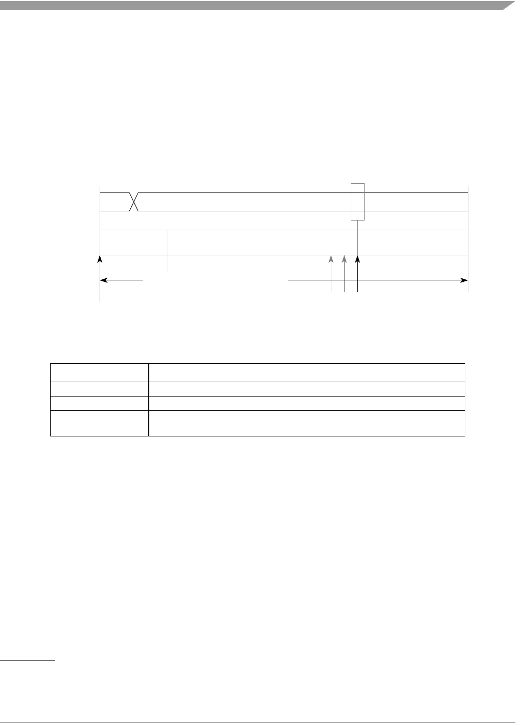
Functional Overview
MCF548x Reference Manual, Rev. 3
Freescale Semiconductor 21-29
• SYNC_SEG: This segment has a fixed length of one time quantum. Signal edges are expected to
happen within this section.
• Time Segment 1: This segment includes the Propagation Segment and the Phase Segment 1 of the
CAN standard. It can be programmed by setting the PROPSEG and the PSEG1 fields of the
CANCTRL register so that their sum (plus 2) is in the range of 4 to 16 time quanta.
• Time Segment 2: This segment represents the Phase Segment 2 of the CAN standard. It can be
programmed by setting the PSEG2 field of the CANCTRL register (plus 1) to be 2 to 8 time quanta
long.
Eqn. 21-1
Figure 21-14. Segments within the Bit Time
Table 21-16 gives an overview of the CAN compliant segment settings and the related parameter values.
NOTE
It is the user’s responsibility to ensure the bit time settings are in compliance
with the CAN standard. For bit time calculations, use an IPT (Information
Processing Time) of 2, which is the value implemented in the FlexCAN
module.
21.4.9.1 Configuring the FlexCAN Bit Timing
The following considerations must be observed when programming bit timing functions:
• If the programmed PRESDIV value results in a single system clock per one time quantum, then the
PSEG2 field in CANCTRL register should not be programmed to zero.
• If the programmed PRESDIV value results in a single system clock per one time quantum, then the
information processing time (IPT) equals three time quanta, otherwise it equals two time quanta.
1. For further explanation of the underlying concepts please refer to ISO/DIS 11519–1, Section 10.3. Reference also the Bosch
CAN 2.0A/B protocol specification dated September 1991 for bit timing.
Table 21-16. Time Segment Syntax
Syntax Description
SYNC_SEG System expects transitions to occur on the bus during this period.
Transmit Point A node in transmit mode transfers a new value to the CAN bus at this point.
Sample Point A node samples the bus at this point. If the three samples per bit option is
selected, then this point marks the position of the third sample.
Bit Rate fTq
(number of Time Quanta)
-------------------------------------------------------------
=
NRZ Signal
Time Segment 1
(PROP_SEG + PSEG1 + 2)
Time Segment 2
(PSEG2 + 1)
SYNC_SEG
1 4 ... 16 2 ... 8
8 ... 25 Time Quanta = 1 Bit Time
Sample Point
(Single or Triple Sampling)
Transmit Point

MCF548x Reference Manual, Rev. 3
21-30 Freescale Semiconductor
If PSEG2 equals two, then the FlexCAN transmits one time quantum late relative to the scheduled
sync segment.
• If the prescaler and bit timing control fields are programmed to values that result in fewer than ten
system clock periods per CAN bit time and the CAN bus loading is 100%, anytime the rising edge
of a start-of-frame (SOF) symbol transmitted by another node occurs during the third bit of the
intermission between messages, the FlexCAN may not be able to prepare a message buffer for
transmission in time to begin its own transmission and arbitrate against the message which
transmitted the early SOF.
• The FlexCAN bit time must be programmed to be greater than or equal to eight system clocks, or
correct operation is not guaranteed. Refer to Application Note AN1798, CAN Bit Timing
Requirements, for more details.
21.4.10 FlexCAN Error Counters
There are two error counters in the FlexCAN: transmit error counter (TXECTR), and receive error counter
(RXECTR). The rules for increasing and decreasing these counters are described in the CAN protocol, and
are fully implemented in the FlexCAN.
Each counter comprises the following:
• 8 bit up/down counter
• Increment by 8 (RXECTR also by 1)
• Decrement by 1
• Avoid decrement when equal to zero
• RXECTR preset to a value 119 ≤ x ≤ 127
• Value after reset = zero
• Detect values for error passive, bus off, and error active transitions and for alerting the host
Both counters are read only (except for freeze and halt modes).
The FlexCAN responds to any bus state as described in the protocol, e.g. transmit error active or error
passive flag, delay its transmission start time (error passive), and avoid any influence on the bus when in
the bus off state. The following are the basic rules for FlexCAN bus state transitions:
• If the value of TXECTR or RXECTR increases to be greater than or equal to 128, the FLTCONF
field in the error status register is updated to reflect it (set error passive state).
• If the FlexCAN state is error passive, and either TXECTR counter or RXECTR then decrements
to a value less than or equal to 127 while the other already satisfies this condition, the
ERRSTAT[FLTCONF] field is updated to reflect it (set error active state).
• If the value of the TXECTR increases to be greater than 255, the ERRSTAT[FLTCONF] field is
updated to reflect it (set bus off state) and an interrupt may be issued. The value of TXECTR is
then reset to zero.
• If the FlexCAN state is bus off, then TXECTR, together with an internal counter are cascaded to
count the 128 occurrences of 11 consecutive recessive bits on the bus. Hence, TXECTR is reset to
zero, and counts in a manner where the internal counter counts 11 such bits and then wraps around
while incrementing the TXECTR. When TXECTR reaches the value of 128,
ERRSTAT[FLTCONF] is updated to be error active, and both error counters are reset to zero. At
any instance of dominant bit following a stream of less than 11 consecutive recessive bits, the
internal counter resets itself to zero, but does not affect the TXECTR value.
• If during system start-up, only one node is operating, then its TXECTR increases with each
message it is trying to transmit as a result of ACKERR. A transition to bus state error passive
should be executed as described, while this device never enters the bus off state.

FlexCAN Initialization Sequence
MCF548x Reference Manual, Rev. 3
Freescale Semiconductor 21-31
• If the RXECTR increases to a value greater than 127, it is no longer incremented, even if more
errors are detected while being a receiver. At the next successful message reception, the counter is
set to a value between 119 and 127, in order to return to error active state.
21.5 FlexCAN Initialization Sequence
Initialization of the FlexCAN includes the initial configuration of the message buffers and configuration
of the CAN communication parameters following a reset, as well as any reconfiguration which may be
required during operation. The following is a generic initialization sequence for the FlexCAN:
1. Initialize all operation modes
a) Initialize the bit timing parameters PROPSEG, PSEGS1, PSEG2, and RJW
in the FlexCAN control register (CANCTRL).
b) Select the S-clock rate by programming the PRESDIV register.
c) Select the internal arbitration mode (CANCTRL[LBUF]).
2. Initialize message buffers
a) The control/status word of all message buffers must be written either as an active or inactive
message buffer.
b) All other entries in each message buffer should be initialized as required.
3. Initialize mask registers for acceptance mask as needed
4. Initialize FlexCAN interrupt handler
a) Initialize the interrupt controller registers for any needed interrupts. See Chapter 13,
“Interrupt Controller,” for more information.
b) Set the required mask bits in the IMASK register (for all message buffer interrupts), in
CANCTRL (for bus off and error interrupts), and in CANMCR for the WAKE interrupt.
5. Clear the HALT bit in the module configuration register
a) At this point, the FlexCAN will attempt to synchronize with the CAN bus.
NOTE
In both the transmit and receive processes, the first action in preparing a
message buffer should be to deactivate the buffer by setting its CODE field
to the proper value. This requirement is mandatory to assure data coherency.
21.5.1 Interrupts
There are four interrupt sources for the FlexCAN module. A combined interrupt for all 16 MBs is
generated by combining all the interrupt sources from MBs. This interrupt gets generated when any of the
16 MB interrupt sources generates a interrupt. In this case, the CPU must read the IFLAG register to
determine which MB caused the interrupt. The other three interrupt sources (bus off, error, and wake-up)
act in the same way, and are located in the error and status register. The bus off and error interrupt mask
bits are located in the CANCTRL register, and the wake-up interrupt mask bit is located in the CANMCR.

MCF548x Reference Manual, Rev. 3
21-32 Freescale Semiconductor

MCF548x Reference Manual, Rev. 3
Freescale Semiconductor 22-1
Chapter 22
Integrated Security Engine (SEC)
This chapter provides an overview of the MCF548x security encryption controller (SEC).
NOTE
Purchasing any of the MCF548x devices with security requires government
export control regulation.
22.1 Features
The SEC is designed to offload computationally intensive security functions, such as authentication bulk
encryption from the MCF548x core. It is optimized to process all the algorithms associated with IPSec,
SSL/TLS, iSCSI, and SRTP.
SEC features include the following:
• DEU—data encryption standard execution unit
— DES, 3DES
— Two key (K1, K2, K1) or three Key (K1, K2, K3)
— ECB and CBC modes for both DES and 3DES
• AESU—advanced encryption standard unit
— Implements the Rinjdael symmetric key cipher
— ECB, CBC, CCM, and counter modes
— 128, 192, 256 bit key lengths
• AFEU—ARC four execution unit
— Implements a stream cipher compatible with the RC4 algorithm
— 40- to 128-bit programmable key
• MDEU—message digest execution unit
— SHA with 160-bit or 256-bit message digest
— MD5 with 128-bit message digest
— HMAC with either algorithm
• RNG—one random number generator
• Master/slave logic, with DMA
— 32-bit address/32 -bit data
— Up to 133 MHz operation
• Two Crypto-channels, each supporting multi-command descriptor chains
— Static and/or dynamic assignment of crypto-execution units via an integrated controller
• Buffer size of 512 bytes for each execution unit, with flow control for large data sizes
22.2 ColdFire Security Architecture
The ability of the SEC to be a master on the internal XLB bus allows the security core to offload the data
movement bottleneck normally associated with slave-only cores.
The ColdFire core accesses the SEC primarily through data packet descriptors using system memory for
data storage. When an application requires cryptographic functions, it simply creates descriptors that
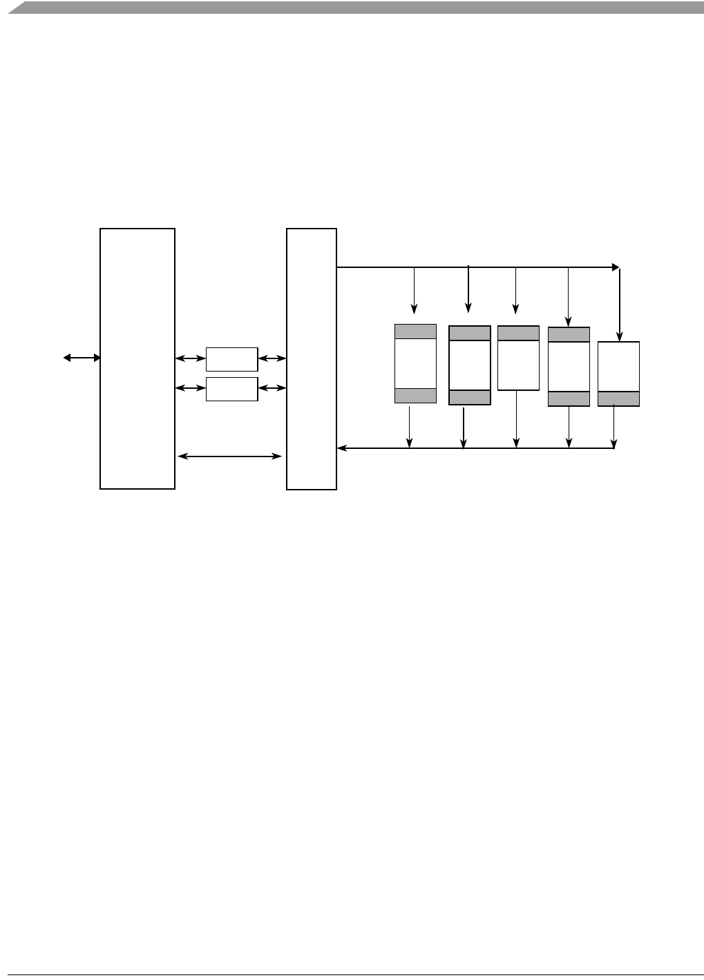
MCF548x Reference Manual, Rev. 3
22-2 Freescale Semiconductor
define the cryptographic function to be performed and the location of the data. The SEC’s bus-mastering
capability permits the host processor to set up a crypto-channel with a few register writes, then the SEC
can perform reads and writes on system memory to fetch data packet descriptors and complete the
specified tasks.
22.3 Block Diagram
Figure 22-1 shows a block diagram of the SEC module. The bus interface module is designed to transfer
32-bit words between the internal bus and any register inside the SEC.
Figure 22-1. SEC Block Diagram
A typical operation consists of the following steps:
• An operation begins with a write of a pointer to a crypto-channel fetch register that points to a data
packet descriptor.
• The channel requests the descriptor and decodes the operation to be performed.
• The channel then requests the controller to assign crypto execution units and fetch the keys,
context/initialization vectors (IVs), and data needed to perform the given operation.
• The controller satisfies the requests by assigning execution units to the channel and by making
requests to the master interface per the programmable priority scheme.
• As data is processed, it is written to the individual execution unit’s output FIFO and then back to
system memory via the bus interface.
22.4 Overview
22.4.1 Bus Interface
The bus interface manages communication between the SEC internal execution units and the internal bus.
The interface uses the bus master/slave protocols. All on-chip resources are memory mapped, and the
target accesses and initiator writes from the SEC must be addressed on longword boundaries. The SEC
will perform initiator reads on byte boundaries and will adjust the data (realign the data) to place on
longword boundaries as appropriate. Access to system memory is a critical factor in co-processor
performance, and the bus interface of the SEC core allows it to achieve performance unattainable on
secondary busses.
FIFO
Crypto-
channel
Crypto-
channel
Control DEU
FIFO
FIFO
FIFO
FIFO
AFEU
Bus
Interface AESU
FIFO
FIFO FIFO
RNG
MDEU

Overview
MCF548x Reference Manual, Rev. 3
Freescale Semiconductor 22-3
22.4.2 SEC Controller Unit
The SEC controller unit manages on-chip resources, including the individual execution units (EUs),
FIFOs, the bus interface, and the internal buses that connect all the various modules. The controller
receives service requests from the bus interface and various crypto-channels, and schedules the required
activities. The controller can configure each of the on-chip resources in two modes:
• Static mode—The user can reserve a specific execution unit to a specific crypto-channel.
• Dynamic mode—A crypto channel can request a particular service from any available execution
unit.
22.4.2.1 Static EU Access
The controller can be configured to assign one or more EUs for a particular crypto-channel. Doing so
permits locking the EU to a particular context. When in this mode, the crypto-channel can be used by
multiple descriptors representing the same context without unloading and reloading the context at the end
of each descriptor. This mode presents considerable performance improvement over dynamic access, but
only when the SEC is supporting few (or one) contexts.
22.4.2.2 Dynamic EU Access
Processing begins when a data packet descriptor pointer is written to the fetch register (FR) of one of the
crypto-channels. First, the controller dynamically reserves usage of an EU to the crypto-channel. If all
appropriate EUs are already dynamically reserved by other crypto-channels, the crypto-channel stalls and
waits to fetch data until an appropriate EU is available. If multiple crypto-channels simultaneously request
the same EU, the EU is assigned on a weighted priority or round-robin basis.
Once the required EU has been reserved, the crypto-channel fetches and loads the appropriate data packets,
operates the EU, unloads data to system memory, and releases the EU for use by another crypto-channel.
If a crypto-channel attempts to reserve a statically-assigned EU (and no appropriate EUs are available for
dynamic assignment), an interrupt is generated and status indicates an illegal access. When dynamic
assignment is used, each encryption/decryption packet descriptor must contain the context and/or keys that
are required for the requested operation.
22.4.3 Crypto-Channels
The SEC includes two crypto-channels that manage data and EU function. Each crypto-channel consists
of the following:
• Control registers containing information about the transaction in process
• A status register containing an indication of the last unfulfilled bus request
• A pointer register indicating the location of a new descriptor to fetch
• Buffer memory used to store the active data packet descriptor
Crypto-channels analyze the data packet descriptor header and requests the first required cryptographic
service from the controller.
After the controller grants access to the required EU, the crypto-channel and the controller perform the
following steps:
1. Set the appropriate mode bits available in the EU for the required service.
2. Fetch context and other parameters as indicated in the data packet descriptor buffer and use these
to program the EU.
3. Fetch data as indicated and place in either the EU input FIFO or the EU itself (as appropriate).

MCF548x Reference Manual, Rev. 3
22-4 Freescale Semiconductor
4. Wait for EU to complete processing.
5. Upon completion, unload results and context and write them to external memory as indicated by
the data packet descriptor.
6. If multiple services requested, go back to step 2.
7. Reset the appropriate EU if it is dynamically assigned. Note that if statically assigned, an EU is
reset only upon direct command written to the SEC.
8. Perform descriptor completion notification as appropriate. This notification comes in one of two
forms—interrupt or header writeback modification—and can occur at the end of every descriptor,
at the end of a descriptor chain, or at the end of specially designated descriptors within a chain.
22.4.4 Execution Units (EUs)
‘Execution unit’ is the generic term for a functional block that performs the mathematical permutations
required by protocols used in cryptographic processing. The EUs are compatible with IPSec, SSL/TLS,
iSCSI, and SRTP processing and can work together to perform high level cryptographic tasks. The SEC
execution units are as follows:
• DEU (data encryption standard execution unit) for performing block cipher, symmetric key
cryptography using DES and 3DES
• AFEU for performing RC-4 compatible stream cipher symmetric key cryptography
• AESU for performing the advanced encryption standard algorithm
• MDEU for performing security hashing using MD-5, SHA-1, or SHA-256
• RNG for random number generation
22.4.4.1 Data Encryption Standard Execution Unit (DEU)
The DES Execution Unit (DEU) performs bulk data encryption/decryption, in compliance with the Data
Encryption Standard algorithm (ANSI x3.92). The DEU can also compute 3DES, an extension of the DES
algorithm in which each 64-bit input block is processed three times. The SEC supports two key (K1=K3)
or three key 3DES.
The DEU operates by permuting 64-bit data blocks with a shared 56-bit key and an initialization vector
(IV). The SEC supports two modes of IV operation: Electronic Code Book (ECB) and Cipher Block
Chaining (CBC).
The DEU module computes the Data Encryption Standard algorithm (ANSI X3.92, FIPS 46-2) for block
type bulk data encryption. It can also execute either the 2-key or the 3-key variants of the Triple-DES
algorithm, which is based on DES. The processor supplies data to the DEU block as input, and the data
will be encrypted and subsequently made available to the processor. The session key is input to the block
prior to encryption.
DES is a block cipher that uses a 56-bit key (64 bits with CRC) to encrypt 64-bit blocks of data, one block
at a time. A conceptual diagram of this process is shown in Figure 22-2. DES is a symmetric algorithm, so
each of the two communicating parties share the same 64-bit key for encryption and decryption. DES
processing begins after this shared session key is agreed upon. The text or binary message to be encrypted
(typically called plaintext) is partitioned into n sets of 64-bit blocks. Each block is processed, in turn, by
the DES engine, producing n sets of encrypted (ciphertext) blocks. These blocks may be transmitted to the
other entity. Decryption is handled in the reverse manner. The ciphertext blocks are processed one at a time
by a DES module in the recipient’s system. The same key is used, and the DES block manages the key
processing internally so that the plaintext blocks are recovered.
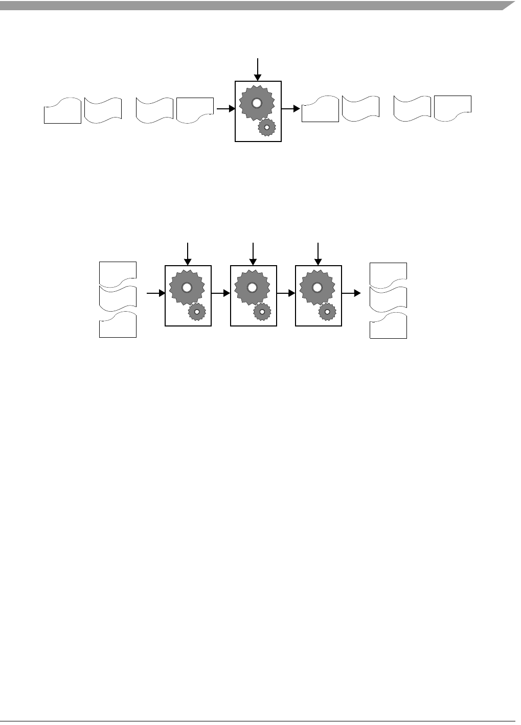
Overview
MCF548x Reference Manual, Rev. 3
Freescale Semiconductor 22-5
Figure 22-2. DES Encryption Process
In addition, the DEU module can compute Triple-DES. Triple-DES is an extension to the DES algorithm
whereby every 64-bit input block is processed three times. A diagram of Triple-DES is shown in
Figure 22-3.
Figure 22-3. Triple-DES Encryption Process (ECB Mode)
22.4.4.2 Arc Four Execution Unit (AFEU)
The AFEU accelerates a bulk encryption algorithm compatible with the RC4 stream cipher from RSA
Security, Inc. The algorithm is byte-oriented, meaning a byte of plaintext is encrypted with a key to
produce a byte of ciphertext. The key is variable length and the AFEU supports key lengths from 40 to 128
bits (in byte increments), providing a wide range of security strengths. ARC4 is a symmetric algorithm,
meaning each of the two communicating parties share the same key.
The AFEU module computes RC4 compatible stream type bulk data encryption. The module processes
eight bytes at a time, producing one byte per three clock cycles; therefore, each 64-bit word requires 24
cycles to process. A symmetric cipher, RC4 relies on a shared key (of variable size) to transform between
plaintext and ciphertext.
Ciphertext/plaintext computation occurs in RC4 by XORing each byte of input text with a
context-dependent output of a substitution box (S-box) to produce output text. The contents of the S-box
are customized based on the input n-bit key, and S-box contents are modified with every byte processed.
The AFEU applies the input stream from and collects the output stream into 8-byte (64-bit) buffers,
providing an interface consistent with other EUs on the SEC.
...
DES
64-bit key
64-bit
block 1
64-bit
block 2
64-bit
block n-1
64-bit
block n
... 64-bit
block 1
64-bit
block 2
64-bit
block n-1
64-bit
block n
Plaintext blocks Ciphertext blocks
DES1
64-bit K1
DES2
64-bit K2
DES3
64-bit K3
64-bit
block 1
64-bit
block n
64-bit
block 1
64-bit
block n
Plaintext blocks
Ciphertext blocks
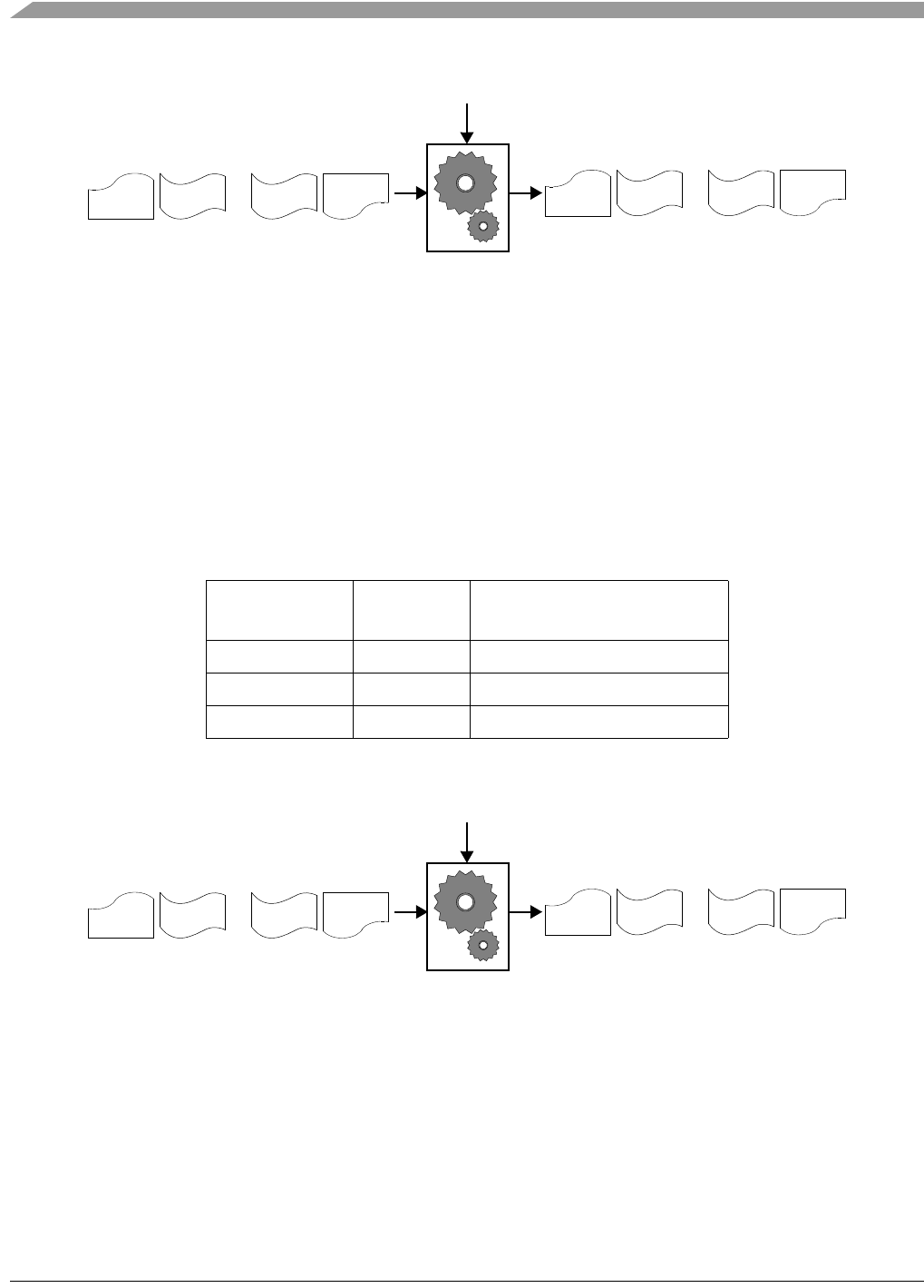
MCF548x Reference Manual, Rev. 3
22-6 Freescale Semiconductor
Figure 22-4. RC4 Encryption Process
22.4.4.3 Advanced Encryption Standard Execution Unit (AESU)
The AESU is used to accelerate bulk data encryption/decryption in compliance with the advanced
encryption standard algorithm (AESA) Rinjdael. The AESU executes on 128 bit blocks with a choice of
key sizes: 128, 192, or 256 bits.
AESU is a symmetric key algorithm, the sender and receiver use the same key for both encryption and
decryption. The session key and initialization vector (CBC mode) are supplied to the AESU module prior
to encryption. The processor supplies data to the module that is processed as 128-bit input. The AESU
engine performs a fixed number of rounds for encryption or decryption depending on the key size.
AESU operates in ECB, CBC, OCB, and CTR modes.
Figure 22-5. AES Encryption Process
22.4.4.4 Message Digest Execution Unit (MDEU)
The MDEU computes a single message digest (or hash or integrity check) value of all the data presented
on the input bus, using either the MD5, SHA-1, or SHA-256 algorithms for bulk data hashing.
• The MD5 generates a 128-bit hash, and the algorithm is specified in RFC 1321.
• SHA-1 is a 160-bit hash function, specified by the ANSI X9.30-2 and FIPS 180-1 standards.
• SHA-256 is a 256-bit hash function that provides 256 bits of security against collision attacks.
Table 22-1. AESA Rounds as a Function of Key Size
Key Size Rounds Cycles
(after initial key expansion)
128 10 11
192 12 13
256 14 15
...
RC4
n-bit key
byte 1byte 2byte n-1byte n ... byte 1byte 2byte n-1byte n
Plaintext stream Ciphertext stream
...
AES
128–256-bit key
128-bit
block 1
128-bit
block 2
128-bit
block n-1
128-bit
block n
... 128-bit
block 1
128-bit
block 2
128-bit
block n-1
128-bit
block n
Plaintext blocks Ciphertext blocks
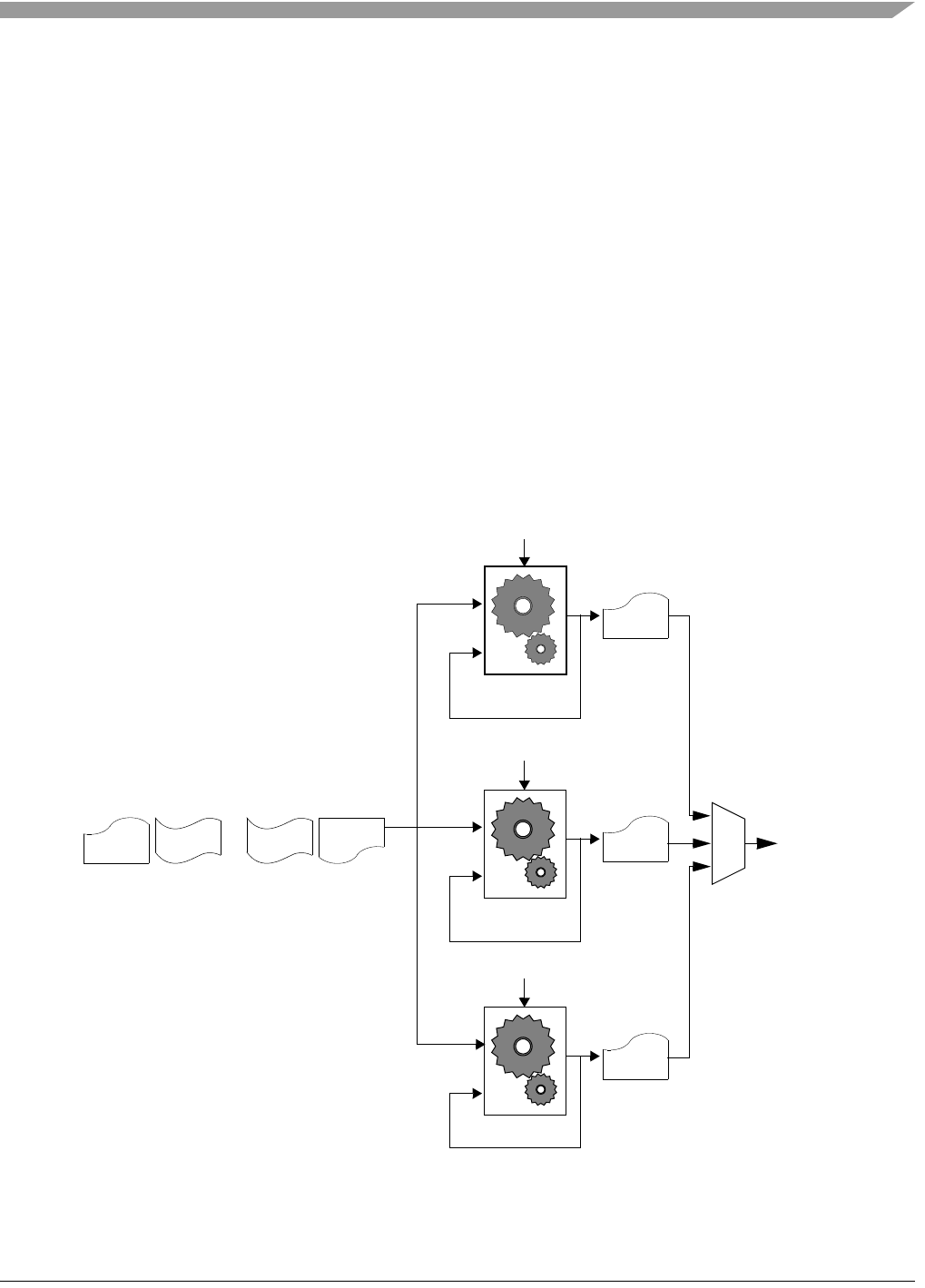
Overview
MCF548x Reference Manual, Rev. 3
Freescale Semiconductor 22-7
• The MDEU also supports HMAC computations, as specified in RFC 2104.
With any hash algorithm, the larger message is mapped onto a smaller output space, therefore collisions
are potential, albeit not probable. The 160-bit hash value is a sufficiently large space such that collisions
are extremely rare. The security of the hash function is based on the difficulty of locating collisions. That
is, it is computationally infeasible to construct two distinct but similar messages that produce the same
hash output.
This block is useful in many applications including hashing messages to generate digital signatures or
computation of a shared secret. The digital signature is typically computed on a small input, however if
the data to be signed is large, it is inefficient to sign the entire data. Instead, the large input data is hashed
to a smaller value which is then signed. If the message is also sent to the verifying authority along with the
signature, the verifying authority can verify the signature by recovering the hash value from the signature
using the public key of the sender, hashing the message itself, and then comparing the computed hash value
with the recovered hash value. If they match, then the verifying authority is confident that the data was
signed by the owner of the private key that matches the public key, where the private key presumably is
only known by the sender. This provides a measure of authentication and non-repudiation.
A conceptual block diagram of the MDEU module is shown in Figure 22-6. Multiple input blocks are
written to the MDEU module, and at the end, the hash value is read as the 160-bit output for SHA-160,
256-bit output for SHA-256, or 128-bit output for MD5.
Figure 22-6. MDEU Hashing Process
...
SHA160
160-bit constant
512-bit
block 1
512-bit
block 2
512-bit
block n-1
512-bit
block n
160-bit
value
Plaintext blocks Hash value
MD5
128-bit constant
128-bit
value
Hash value
Output
Register
SHA256
256-bit constant
256-bit
value
Hash value

MCF548x Reference Manual, Rev. 3
22-8 Freescale Semiconductor
22.4.4.5 Random Number Generator (RNG)
The RNG is a digital integrated circuit capable of generating 32-bit random numbers. It is designed to
comply with FIPS 140-1 standards for randomness and non-determinism.
Because many cryptographic algorithms use random numbers as a source for generating a secret value (a
nonce), it is desirable to have a private RNG for use by the SEC. The anonymity of each random number
must be maintained, as well as the unpredictablility of the next random number. The FIPS-140 ‘common
criteria’ compliant private RNG allows the system to develop random challenges or random secret keys.
The secret key can thus remain hidden from even the high-level application code, providing an added
measure of physical security.
The random number generator is responsible for creating an unpredictable sequence of bits and assembling
a string of those bits into a FIFO.
22.5 Memory Map/Register Definition
This section contains the SEC address map. Many of the registers are defined as 64-bit wide, but can be
addressed as two longword registers. For example, bits 63–32 of the EU assignment control register are
accessed at an MBAR offset of 0x21000. Bits 31–0 are accessed at an MBAR offset of 0x21004.
Table 22-2 shows the base address map for the modules within the SEC.
Table 22-3 provides the precise address map, including all registers in the execution units. The last column
of the table provides a cross reference to the section where the register is described in detail.
Table 22-2. SEC Module Base Address Map
MBAR Offset SEC Module Description Type
0x20000–0x200FF — Reserved —
0x21000–0x21FFF Controller Arbiter/Controller Control register space Resource Control
0x22000–0x22FFF Channel_1 Crypto-channel 1 Data Control
0x23000–0x23FFF Channel_2 Crypto-channel 2 Data Control
0x24000–0x26FFF — Reserved —
0x28000–0x28FFF AFEU ArcFour Execution Unit Crypto EU
0x2A000–0x2AFFF DEU DES Execution Unit Crypto EU
0x2C000–0x2CFFF MDEU Message Digest Execution Unit Crypto EU
0x2E000–0x2EFFF RNG Random Number Generator Crypto EU
0x32000–0x32FFF AESU AES Execution Unit Crypto EU
Table 22-3. SEC Register Map
Register
Offset Mnemonic Name Page
Controller Registers
0x21000 EUACRH EU Assignment Control Register High p. 22-11
0x21004 EUACRL EU Assignment Control Register Low p. 22-11

Memory Map/Register Definition
MCF548x Reference Manual, Rev. 3
Freescale Semiconductor 22-9
0x21008 SIMRH SEC Interrupt Mask Register High p. 22-14
0x2100C SIMRL SEC Interrupt Mask Register Low p. 22-14
0x21010 SISRH SEC Interrupt Status Register High p. 22-14
0x21014 SISRL SEC Interrupt Status Register Low p. 22-14
0x21018 SICRH SEC Interrupt Control Register High p. 22-14
0x2101C SICRL SEC Interrupt Control Register Low p. 22-14
0x21020 SIDR SEC ID Register p. 22-16
0x21028 EUASRH EU Assignment Status Register High p. 22-13
0x2102C EUASRL EU Assignment Status Register Low p. 22-13
0x21030 SMCR SEC Master Control Register p. 22-17
0x21038 MEAR Master Error Address Register p. 22-18
Crypto-Channel 0 (CC0) Registers
0x2200C CCCR0 Crypto-Channel Configuration Register 0 p. 22-19
0x22010 CCPSRH0 Crypto-Channel Pointer Status Register High 0 p. 22-21
0x22014 CCPSRL0 Crypto-Channel Pointer Status Register Low 0 p. 22-21
0x22044 CDPR0 Crypto-Channel Current Descriptor Pointer Register 0 p. 22-27
0x2204C FR0 Fetch Register 0 p. 22-27
0x22080–
0x220BF
CDBUF0 Crypto-Channel Descriptor Buffer 0 p. 22-28
Crypto-Channel 1 (CC1) Registers
0x2200C CCCR1 Crypto-Channel Configuration Register 1 p. 22-19
0x22010 CCPSRH1 Crypto-Channel Pointer Status Register High 1 p. 22-21
0x22014 CCPSRL1 Crypto-Channel Pointer Status Register Low 1 p. 22-21
0x22044 CDPR1 Crypto-Channel Current Descriptor Pointer Register 1 p. 22-27
0x2204C FR1 Fetch Register 1 p. 22-27
0x22080–
0x220BF
CDBUF1 Crypto-Channel Descriptor Buffer 1 p. 22-28
AFEU Registers
0x28018 AFRCR AFEU Reset Control Register p. 22-28
0x28028 AFSR AFEU Status Register p. 22-29
0x28030 AFISR AFEU Interrupt Status Register p. 22-31
0x28038 AFIMR AFEU Interrupt Mask Register p. 22-32
Table 22-3. SEC Register Map (Continued)
Register
Offset Mnemonic Name Page

MCF548x Reference Manual, Rev. 3
22-10 Freescale Semiconductor
22.6 Controller
The controller within the SEC core is responsible for overseeing the operations of the EUs, the interface
to the host processor, and the management of the crypto-channels. The controller interfaces to the host via
the bus interface and to the channels and EUs via internal buses.
All transfers between the host and the EUs are moderated by the controller. Some of the main functions of
the controller are as follows:
• Arbitrate and control accesses to the ColdFire bus
• Control the internal bus accesses to the EUs
• Arbitrate and assign EUs to the crypto-channels
• Monitor interrupts from channels and pass to host
• Realign initiator read data to 64-bit boundary
DEU Registers
0x2A018 DRCR DEU Reset Control Register p. 22-34
0x2A028 DSR DEU Status Register p. 22-35
0x2A030 DISR DEU Interrupt Status Register p. 22-37
0x2A038 DIMR DEU Interrupt Mask Register p. 22-39
MDEU Registers
0x2C018 MDRCR MDEU Reset Control Register p. 22-41
0x2C028 MDSR MDEU Status Register p. 22-41
0x2C030 MDISR MDEU Interrupt Status Register p. 22-43
0x2C038 MDIMR MDEU Interrupt Mask Register p. 22-44
RNG Registers
0x2E018 RRCR RNG Reset Control Register p. 22-46
0x2E028 RSR RNG Status Register p. 22-47
0x2E030 RISR RNG Interrupt Status Register p. 22-48
0x2E038 RIMR RNG Interrupt Mask Register p. 22-49
AESU Registers
0x32018 AESRCR AESU Reset Control Register p. 22-50
0x32028 AESSR AESU Status Register p. 22-51
0x32030 AESISR AESU Interrupt Status Register p. 22-53
0x32038 AESIMR AESU Interrupt Mask Register p. 22-54
Table 22-3. SEC Register Map (Continued)
Register
Offset Mnemonic Name Page

Controller
MCF548x Reference Manual, Rev. 3
Freescale Semiconductor 22-11
22.6.1 EU Access
Assignment of an EU function to a channel is done either statically or dynamically. In the case of static
assignment, an EU is assigned to a channel via the EU Assignment Control Register (EUACR). Once an
EU is statically assigned to a channel, it will remain that way until the EUACR is written and the
assignment is removed.
In the case of dynamic assignment, the channel requests an EU function, the controller checks to see if the
requested EU function is available, and if it is, the controller grants the channel assignment of the EU.
22.6.2 Multiple EU Assignment
In some cases, a channel may request two EUs. The channel will do this by first requesting the primary
EU, then requesting the secondary EU. Once the controller has granted both EUs, this channel is then
capable of requesting that the secondary EU snoop the bus. Snooping is described in Table 22-14.
In all cases, the controller assigns the primary EU to a requesting channel as the EUs become available.
The controller does not wait until both EUs are available before issuing any grants to a channel which is
requesting two EU functions.
22.6.3 Multiple Channels
Since there are multiple channels in the SEC, the controller must arbitrate for access to the execution units.
Because a channel cannot make instantaneous resource requests, the arbiter in the controller will toggle
between channel 1 and channel 2, assuming that both channels are contesting for a given resource, such as
the external bus or a particular EU.
22.6.4 Controller Registers
The controller contains the following registers, which are described in detail in the following sections.
• EU assignment control register (EUACR)
• EU assignment status register (EUASR)
• SEC interrupt mask register (SIMR)
• SEC interrupt status register (SISR)
• SEC interrupt control register (SICR)
• SEC ID register (SIDR)
• SEC master control register (SMCR)
• Master error address register (MEAR)
22.6.4.1 EU Assignment Control Registers (EUACRH and EUACRL)
These registers are used to make a static assignment of a EU to a particular crypto-channel. When assigned
in this fashion, the EU is inaccessible to any other crypto-channel.
NOTE
The EU assignment control registers (EUACRH and EUACRL) are used to
make, and therefore will reflect, only static assignments.

MCF548x Reference Manual, Rev. 3
22-12 Freescale Semiconductor
Table 22-4 describes the EUACRH and EUACRL fields.
31 30 29 28 27 26 25 24 23 22 21 20 19 18 17 16
Field — RNG — —
Reset 1111 0000 1111 0000
R/W R R/W R R
1514131211109876543210
Field — MDEU — AFEU
Reset 1111 0000 1111 0000
R/W R R/W R R/W
Reg
Addr
MBAR + 0x21000
Figure 22-7. EU Assignment Control Register High (EUACRH)
31 30 29 28 27 26 25 24 23 22 21 20 19 18 17 16
Field — DEU — AESU
Reset 1111 0000 1111 0000
R/W R R/W R R/W
1514131211109876543210
Field — — —
Reset 1111 1111 0000
R/W R R R
Reg
Addr
MBAR + 0x21004
Figure 22-8. EU Assignment Control Register Low (EUACRL)
Table 22-4. EUACRH and EUACRL Field Descriptions
Bits Name Description
31–0 See
Figure 22-8
Static Channel Assignment. Each field corresponds to one of the SEC EUs. The field
indicates if the EU is currently assigned to one of the two channels as shown in Table 22- 5.
Writing any of the defined values shown in Table 22-5 to any of the fields in the EUACR
statically assigns the EU to that specific channel. To release, the host must write 0x0 to the
specified EU field of the EUACR.
Table 22-5. Channel Assignment Value
Value Channel
0x0 No channel assigned
0x1 Channel 0
0x2 Channel 1

Controller
MCF548x Reference Manual, Rev. 3
Freescale Semiconductor 22-13
22.6.4.2 EU Assignment Status Registers (EUASRH and EUASRL)
The EUASR registers, shown in Figure 22-9 and Figure 22-10, are used to check the assignment status
(static or dynamic) of an EU to a particular crypto-channel. When an EU is already assigned, it is
inaccessible to any other crypto-channel.
A four-bit field indicates the channel to which an EU is assigned, whether statically or dynamically.
0x3–0xE Reserved
0xF EU is not statically assigned to any channel and is not
allowed to be dynamically assigned to a channel.
31 30 29 28 27 26 25 24 23 22 21 20 19 18 17 16
Field — RNG — —
Reset 1111 0000 1111 0000
R/W R R/W R R
1514131211109876543210
Field — MDEU — AFEU
Reset 1111 0000 1111 0000
R/W R R/W R R/W
Reg
Addr
MBAR + 0x21028
Figure 22-9. EU Assignment Status Register High (EUASRH)
31 30 29 28 27 26 25 24 23 22 21 20 19 18 17 16
Field — DESU — AESU
Reset 1111 0000 1111 0000
R/W R R/W R R/W
1514131211109876543210
Field — — —
Reset 1111 1111 0000
R/W R R R
Reg
Addr
MBAR + 0x2102C
Figure 22-10. EU Assignment Status Register Low (EUASRL)
Table 22-5. Channel Assignment Value (Continued)
Value Channel

MCF548x Reference Manual, Rev. 3
22-14 Freescale Semiconductor
22.6.4.3 SEC Interrupt Mask Registers (SIMRH and SIMRL)
The SEC generates a single interrupt output from all possible interrupt sources. These sources can be
masked by the SIMR registers. If unmasked, the interrupt source value, when active, is captured into the
SEC interrupt status registers (SISRH and SISRL). Figure 22-11 and Figure 22-12 show the bit positions
of each potential interrupt source. Each interrupt source is individually masked by setting it’s
corresponding bit.
22.6.4.4 SEC Interrupt Status Registers (SISRH and SISRL)
The SEC interrupt status registers contain fields representing all possible sources of interrupts. The SISR
is cleared either by a reset, or by writing the appropriate bits active in the SEC interrupt control registers
(SICRH and SICRL). Figure 22-11 and Figure 22-12 shows the bit positions of each potential interrupt
source.
22.6.4.5 SEC Interrupt Control Registers (SICRH and SICRL)
The SEC interrupt control registers (SICRH and SICRL) provide a means of clearing the SISR registers.
When a bit in either SICR is written with a 1, the corresponding bit in the SISR is cleared, clearing the
interrupt output pin IRQ (assuming the cleared bit in the SISR is the only interrupt source). If the input
source to the SISR is a steady-state signal that remains active, the appropriate SISR bit, and subsequently
IRQ, will be reasserted shortly thereafter. The complete bit definitions for the SICR can be found in
Figure 22-11 and Figure 22-12.
When an SICR bit is written, it will automatically clear itself one cycle later. That is, it is not necessary to
write a 0 to a bit position which has been written with a 1.
NOTE
Interrupts are registered and sent based upon the conditions which cause
them. If the cause of an interrupt is not removed, the interrupt will return a
few cycles after it has been cleared using the SICR.
Table 22-6. EUASRH and EUASRL Field Descriptions
Bits Name Description
31–0 See Figure 22-10 Channel Assignment. Each field corresponds to one of the SEC EUs. The field indicates if
the EU is currently assigned to one of the two channels as shown in Table 2 2- 5.

Controller
MCF548x Reference Manual, Rev. 3
Freescale Semiconductor 22-15
I
31 30 29 28 27 26 25 24 23 22 21 20 19 18 17 16
Field CHA_1 CHA_0 AERR —
Definition ERR DN ERR DN
Reset 0x0000
R/W W
1514131211109876543210
Field —
Definition
Reset 0x0000
R/W W
Reg
Addr
MBAR + 0x21008 (SIMRH), 0x 21010 (SISRH), 0x21018 (SICRH)
Figure 22-11. SEC Interrupt Mask, Status, and Control Registers High (SIMRH, SISRH, and SICRH)
Table 22-7. SIMRH, SISRH, and SICRH Field Descriptions
Bits Name Description
31, 29 CH_n_ERR_DN Channel error. Each of the channels has an error bit.
0 No error detected.
1 Error detected. Indicates that execution unit status register must be read to determine
exact cause of the error.
30, 28 CH_n_DN Channel done. Each of the channels has a done bit.
0 Not DONE.
1 DONE bit indicates that the interrupting channel or EU has completed its operation.
27 AERR Assignment Error bit. This bit indicates that a static assignment of a EU was attempted
on a EU which is currently in use.
0 No error detected.
1 EU Assignment Error detected.
26–0 — Reserved, should be cleared.

MCF548x Reference Manual, Rev. 3
22-16 Freescale Semiconductor
22.6.4.6 SEC ID Register (SIDR)
The read-only SEC ID register, displayed in Figure 22-13, contains a 32-bit value that uniquely identifies
the version of the SEC. The value of this register is always 0x0900_0000.
31 30 29 28 27 26 25 24 23 22 21 20 19 18 17 16
Field — RNG — AFEU — MDEU
Definition ERR DN ERR DN ERR DN
Reset 0x0000
R/W R/W
1514131211109876543210
Field — AESU — DEU — TEA —
Definition ERR DN ERR DN
Reset 0x0000
R/W R/W
Reg
Addr
MBAR + 0x2100C (SIMRL), 0x 21014 (SISRL), 0x2101C (SICRL)
Figure 22-12. SEC Interrupt Mask, Status, and Control Registers Low (SIMRL, SISRL, and SICRL)
Table 22-8. SIMRL, SISRL, and SICRL Field Descriptions
Bits Name Description
31–26 — Reserved, should be cleared.
25, 21, 17,
13, 9
EU_x_ERR EU error. Each of the execution units has an error bit.
0 No error detected.
1 Error detected. Indicates that execution unit status register must be read to determine
exact cause of the error.
24, 20, 16,
12, 8
EU_x_DN EU done. Each of the execution units has a done bit.
0 Not DONE.
1 DONE bit indicates that the interrupting channel or EU has completed its operation.
23–22,
19–18,
15–14,
11–10, 7
— Reserved, set to zero.
6 TEA Transfer Error Acknowledge. Set when the SEC as a master receives a Transfer Error
Acknowledge.
0 No error detected.
1 TEA detected on Coldfire bus.
5–0 — Reserved, set to zero.

Controller
MCF548x Reference Manual, Rev. 3
Freescale Semiconductor 22-17
22.6.4.7 SEC Master Control Register (SMCR)
The SEC master control register (SMCR), shown in Figure 22-14, controls certain functions in the
controller and provides a means for software to reset the SEC.
31 30 29 28 27 26 25 24 23 22 21 20 19 18 17 16
RVersion
W
Reset0000100100000000
1514131211109876543210
RVersion
W
Reset0000000000000000
Reg
Addr
MBAR + 0x 21020
Figure 22-13. ID Register (SIDR)
31 30 29 28 27 26 25 24 23 22 21 20 19 18 17 16
R0000000SWR00000000
W
Reset0000000000000000
1514131211109876543210
R00000000 CURR_CHAN 0000
W
Reset0000000000000000
Reg
Addr
MBAR + 0x 21030
Figure 22-14. SEC Master Control Register (SMCR)
Table 22-9. SMCR Field Descriptions
Bits Name Description
31–25 — Reserved
24 SWR Software Reset. Writing 1 to this bit will cause a global software reset. Upon
completion of the reset, this bit will be automatically cleared.
0 Don’t reset
1 Global Reset
23–8 — Reserved

MCF548x Reference Manual, Rev. 3
22-18 Freescale Semiconductor
22.6.4.8 Master Error Address Register (MEAR)
This register saves the address of the transaction whose data phase was terminated with a TEA or Master
Parity Error. A Transfer Error Acknowledge (TEA) signal indicates a fatal error has occurred during the
data phase of a bus transaction. Invalid data may have been received and stored prior to the receipt of the
TEA. The channel that was initiating the transaction will be evident from that channel’s error interrupt.
Software may chose to reset the channel reporting the TEA, reset the whole SEC, or reset the entire system.
In any case, the host may chose to preserve this TEA information prior to reset to assist in debug.
The MEAR only holds the address of the first error reported, in the event multiple errors are received
before the first is cleared.
Table 22-10 defines the MEAR fields.
22.7 Channels
A crypto-channel manages data associated with the one or more execution units (EUs). Control and data
information for a given task is stored in the form of data packet descriptors in system memory. The
descriptor describes how the EU should be initialized, where to fetch the data to be ciphered and where to
7–4 CURR_CHAN Current Channel. These bits are read only. They indicate the channel number that is
currently in use by the controller as a master on the XLB bus. The possible values are:
0000 - No Channel is currently in use.
0001 - Channel 0 is in use.
0010 - Channel 1 is in use.
3–0 — Reserved
31 30 29 28 27 26 25 24 23 22 21 20 19 18 17 16
RAddress
W
Reset0000000000000000
1514131211109876543210
RAddress
W
Reset0000000000000000
Reg
Addr
MBAR + 0x 21038
Figure 22-15. Master Error Address Register (MEAR)
Table 22-10. MEAR Field Descriptions
Bits Name Description
31–0 ADDRESS Target address of the transaction when TEA was received.
Table 22-9. SMCR Field Descriptions (Continued)
Bits Name Description

Channels
MCF548x Reference Manual, Rev. 3
Freescale Semiconductor 22-19
store the ciphered data the EU outputs. Through a series of requests to the controller, the crypto-channel
decodes the contents of the descriptors to perform the following functions:
• Request assignment of one or more of the several EUs for the exclusive use of the channel.
• Request assignment of the MDEU when the descriptor header calls for multi-operation processing.
The MDEU will be configured to snoop input or output data intended for the primary assigned EU.
• Reset assigned EU(s).
• Automatically initialize mode registers in the assigned EU upon notification of completion of the
EU reset sequence.
• Automatically initialize the key and key size in the assigned EU after requesting a write to EU key
address space.
• Automatically initialize data size in the assigned EU before requesting a write to EU FIFO address
space.
• Transfer data packets (up to 32Kbytes) from system memory (master read) into assigned EU input
registers and FIFOs (EU write).
• Transfer data packets (up to 32Kbytes) from assigned EU output registers and FIFOs (EU read) to
system memory space (master write).
• Release assigned EU(s).
• Automatically fetch the next descriptor from system memory and start processing, when chaining
is enabled. Descriptor chains can be of unlimited size.
• Provide feedback to host, via interrupt, when a descriptor, or a chain of descriptors, has been
completely processed.
• Provide feedback to host, via modified descriptor header write back to system memory, when a
descriptor, or a chain of descriptors, has been completely processed.
• Provide feedback to host, via interrupt, when descriptor processing is halted due to an error.
• Detect static assignment of EU(s) by the controller and alter descriptor processing flow to skip EU
request and EU release steps. The channel will also automatically reset the EU_DONE interrupt
after receiving indication that processing of input data has been completed by the EU.
The channel will wait indefinitely for the controller to complete a requested activity before continuing to
process a descriptor.
22.7.1 Crypto-Channel Registers
Each crypto-channel contains the following registers:
• Crypto-channel configuration register (CCCRn)
• Crypto-channel pointer status register (CCPSRn)
• Current descriptor pointer register (CDPRn)
• Fetch register (FRn)
• Data packet descriptor buffer (CFBUFn)
22.7.1.1 Crypto-Channel Configuration Registers (CCCRn)
This register contains five operational bits permitting configuration of the crypto-channel as shown in
Figure 22-16.

MCF548x Reference Manual, Rev. 3
22-20 Freescale Semiconductor
31 30 29 28 27 26 25 24 23 22 21 20 19 18 17 16
R0000000000000000
W
Reset0000000000000000
15 14 13 12 11 10 9 8 7 6 5 4 3 2 1 0
R00000 BURST_SIZE 000WENENTCDIERST
W
Reset0000000000000000
Reg
Addr
MBAR + 0x2200C (CCCR0), 0x2300C (CCCR1)
Figure 22-16. Crypto-Channel Configuration Register (CCCRn)
Table 22-11. CCCRn Field Descriptions
Bits Name Description
31–11 — Reserved, should be cleared.
10–8 BURST SIZE The SEC implements flow control to allow larger than FIFO sized blocks of data to be
processed with a single key/IV. The channel programs the various execution units to advise on
space or data available in the FIFO via this field. The size of the burst is given in Table 22-12
7–5 — Reserved, should be cleared.
4 WE Writeback Enable. This bit determines if the crypto-channel is allowed to notify the host of the
completion of descriptor processing by writing back a value of 0xFF to the first byte of the
descriptor header. This enables the host to poll the memory location of the original descriptor
header to determine if that descriptor has been completed.
0 Descriptor header writeback notification is disabled.
1 Descriptor header writeback notification is enabled.
Note: Header writeback notification will occur at the end of every descriptor if
NOTIFICATION_TYPE is set to end-of-descriptor and Writeback_Enable is set. Writeback will
occur only after the last descriptor in the chain (Next Descriptor Pointer is NULL) if
NOTIFICATION_TYPE is set to end-of-chain.
3 NE Fetch Next Descriptor Enable. This bit determines if the crypto-channel is allowed to request
a transfer of the next descriptor, in a multi-descriptor chain, into its descriptor buffer.
0 Disable fetching of next descriptor when crypto-channel has finished processing the current
one.
1 Enable fetching of next descriptor when crypto-channel has finished processing the current
one.
The address of the next descriptor in a multi-descriptor chain is either the contents of the next
descriptor pointer in the descriptor buffer or the contents of the fetch register. Only if both of
these registers are NULL upon completion of the descriptor currently being processed will that
descriptor be considered the end of the chain.

Channels
MCF548x Reference Manual, Rev. 3
Freescale Semiconductor 22-21
Table 22-12 defines the burst size according to the value displayed in the BURST_SIZE field.
22.7.1.2 Crypto-Channel Pointer Status Registers (CCPSRHn and CCPSRLn)
These registers contain status fields and counters which provide the user with status information regarding
the channel’s actual processing of a given descriptor.
2 NT Channel DONE Notification Type. This bit controls when the crypto-channel will generate
Channel DONE Notification.
0 End-of-chain: The crypto-channel will generate channel done notification (if enabled) when
it completes the processing of the last descriptor in a descriptor chain. The last descriptor
is identified by having NULL loaded into both the next descriptor pointer in the descriptor
buffer and the fetch register.
1 End-of-descriptor: The crypto-channel will generate channel done notification (if enabled) at
the end of every data descriptor it processes
Channel DONE notification can take the form of an interrupt or modified header writeback or
both, depending on the state of the CDIE and WE control bits.
1 CDIE Channel DONE Interrupt Enable. This bit determines whether or not the crypto-channel is
allowed to assert interrupts to notify the host that the channel has completed descriptor
processing.
0 Channel Done interrupt disabled
1 Channel Done interrupt enabled
When CDIE is set, the NT control bit determines when the CHANNEL_DONE interrupt is
asserted. Channel error interrupts are asserted as soon as the error is detected.
0 RST Reset Crypto-Channel. This bit allows for a software reset of the crypto-channel.
0 Automatically cleared by the crypto-channel when reset sequence is complete.
1 Reset the registers and internal state of the crypto-channel, any EU assigned to the
crypto-channel and the controller state associated with the crypto-channel.
Table 22-12. Burst Size Definition
Value Number of Longwords in Burst
000 2
001 8
010 16
011 24
100 32
101 40
110 48
111 56
Table 22-11. CCCRn Field Descriptions (Continued)
Bits Name Description

MCF548x Reference Manual, Rev. 3
22-22 Freescale Semiconductor
31 30 29 28 27 26 25 24 23 22 21 20 19 18 17 16
R0000000000000000
W
Reset0000000000000000
1514131211109876543210
R00000000 STATE
W
Reset0000000000000000
Reg
Addr
MBAR + 0x22010 (CCPSRH0), 0x23010 (CCPSRH1)
Figure 22-17. Crypto-Channel Pointer Status Register High (CCPSRHn)
Table 22-13. CCPSRHn Field Descriptions
Bits Name Description
31–8 — Reserved, set to zero.
7–0 STATE State of the crypto-channel state machine. This field reflects the state of the crypto-channel
control state machine. The value of this field indicates exactly which stage the crypto-channel
is in the sequence of fetching and processing data descriptors. Table 22-15 shows the
meaning of all possible values of the STATE field.
State is documented for information only. The user will not typically care about the
crypto-channel state machine.
31 30 29 28 27 26 25 24 23 22 21 20 19 18 17 16
R0 0 0 0 0STATMI MO PRSRPGSGPRDSRDPDSD
W
Reset0000000 0 00000000
15 14 13 12 11 10 9 8 7 6 5 4 3 2 1 0
R 0 0 TEA PERR 0 DERR SERR EUERR PAIR_PTR
W
Reset0000000 0 00000111
Reg
Addr
MBAR + 0x22014 (CCPSRL0), 0x23014 (CCPSRL1)
Figure 22-18. Crypto-Channel Pointer Status Register Low (CCPSRLn)

Channels
MCF548x Reference Manual, Rev. 3
Freescale Semiconductor 22-23
Table 22-14. CCPSRLn Field Descriptions
Bits Name Description
31–27 — Reserved, set to zero
26 STAT Crypto-Channel Static Mode Enable. The STAT bit is set when descriptor processing is
initiated and the EUs indicated in the descriptor header register are already assigned to the
channel. This bit is cleared when descriptor processing is initiated for the next descriptor and
no EUs are assigned to the channel.
0 Crypto-channel is operating in dynamic mode.
1 Crypto-channel is operating in static mode.
25 Multi_EU_IN Multi_EU_IN. Reflects the type of snooping the channel will perform, as programmed by the
“Snoop Type” bit in the descriptor header.
0 Data input snooping by secondary EU disabled.
1 Data input snooping by secondary EU enabled.
24 Multi_EU_OUT Multi_EU_OUT. Reflects the type of snooping the channel will perform, as programmed by the
“Snoop Type” bit in the descriptor header.
0 Data output snooping by secondary EU disabled.
1 Data output snooping by secondary EU enabled.
23 PR Primary request. Request primary EU assignment.
0 Primary EU Assignment Request is inactive.
1 The crypto-channel is requesting assignment of primary EU to the channel. The channel
will assert the EU request signal indicated by the PEUSEL field in the descriptor header as
long as this bit remains set.
The PR bit is set when descriptor processing is initiated in dynamic mode and the PEUSEL
field in the descriptor header contains a valid EU identifier. This bit is cleared when the request
is granted, which will be reflected in the status register by the setting the PG bit.
22 SR Secondary request. Request secondary EU assignment.
0 Secondary EU Assignment Request is inactive.
1 The crypto-channel is requesting assignment of secondary EU to the channel. The channel
will assert the EU request signal indicated by the SEUSEL field in the descriptor header
register as long as this bit remains set.
The SR bit is set when descriptor processing is initiated in dynamic mode and the SEUSEL
field in the descriptor header contains a valid EU identifier. This bit is cleared when the request
is granted, which will be reflected in the status register by the setting the SG bit.
21 PG Primary EU granted. Reflects the state of the EU grant signal for the requested primary EU
from the controller.
0 The primary EU grant signal is inactive.
1 The EU grant signal is active indicating the controller has assigned the requested primary
EU to the channel.
20 SG Secondary EU granted. Reflects the state of the EU grant signal for the requested secondary
EU from the controller.
0 The secondary EU grant signal is inactive.
1 The EU grant signal is active indicating the controller has assigned the requested
secondary EU to the channel.
19 PRD Primary EU reset done. Reflects the state of the reset done signal from the assigned primary
EU.
0 The assigned primary EU reset done signal is inactive.
1 The assigned primary EU reset done signal is active indicating its reset sequence has
completed and it is ready to accept data.

MCF548x Reference Manual, Rev. 3
22-24 Freescale Semiconductor
18 SRD Secondary EU reset done. Reflects the state of the reset done signal from the assigned
secondary EU.
0 The assigned secondary EU reset done signal is inactive.
1 The assigned secondary EU reset done signal is active indicating its reset sequence has
completed and it is ready to accept data.
17 PD Primary EU done. Reflects the state of the done interrupt from the assigned primary EU.
0 The assigned primary EU done interrupt is inactive.
1 The assigned primary EU done interrupt is active indicating the EU has completed
processing and is ready to provide output data.
16 SD Secondary EU done. Reflects the state of the done interrupt from the assigned secondary EU.
0 The assigned secondary EU done interrupt is inactive.
1 The assigned secondary EU done interrupt is active indicating the EU has completed
processing and is ready to provide output data.
15–14 — Reserved, should be cleared.
13 TEA Transfer error acknowledge. When the SEC is a bus master and detects a TEA, the controller
passes the TEA to the channel in use. The channel halts and outputs an interrupt. The channel
can only be restarted by resetting the channel or the entire SEC.
0 No error.
1 Transfer error acknowledge received from the bus interface.
12 PERR Pointer not complete error. Caused by an invalid write to the next descriptor register in the
descriptor buffer, or to the fetch register.
0 No error.
1 Pointer not complete error.
11 — Reserved, should be cleared.
10 DERR Descriptor error. The channel has detected an illegal descriptor header.
0 No error.
1 Descriptor error.
9 SERR Static assignment error. Either the EU is statically assigned to a different channel or the
dynamic assignment request cannot be filled because all suitable EUs are otherwise statically
assigned.
0 No error.
1 Static assignment error.
Table 22-14. CCPSRLn Field Descriptions (Continued)
Bits Name Description

Channels
MCF548x Reference Manual, Rev. 3
Freescale Semiconductor 22-25
Table 22-15 shows the values of crypto-channel states.
8 EUERR EU error. An EU assigned to this channel has generated an error interrupt. This error may also
be reflected in the controller’s SISR. The EUERR bit can only be cleared by first clearing the
error source in the assigned EU which caused it to be set.
0 No error.
1 EU error.
7–0 PAIR_PTR Descriptor buffer register length/pointer pair. This field indicates which of the length/pointer
pairs are currently being processed by the channel.
0x0 Processing header or length/pointer pair 0.
0x1 Processing length/pointer pair 1.
0x2 Processing length/pointer pair 2.
0x3 Processing length/pointer pair 3.
0x4 Processing length/pointer pair 4.
0x5 Processing length/pointer pair 5.
0x6 Processing length/pointer pair 6.
0x7 Complete (or not yet begun) processing of header and length/pointer pairs
0x8-0xFF Reserved
Table 22-15. STATE Field Values
Value Crypto-Channel State
0x00 Idle
0x01 Processing header
0x02 Fetching descriptor
0x03 Channel done
0x04 Channel done irq
0x05 Channel done writeback
0x06 Channel done notification
0x07 Channel_error
0x08 Request primary EU
0x09 Inc data pair pointer
0x0A Delay data pair update
0x0B Evaluate data pairs
0x0C Write reset primary
0x0D Release primary EU
0x0E Write reset secondary
0x0F Release secondary EU
0x10 Process data pairs
0x11 Write mode primary
Table 22-14. CCPSRLn Field Descriptions (Continued)
Bits Name Description

MCF548x Reference Manual, Rev. 3
22-26 Freescale Semiconductor
0x12 Write mode secondary
0x13 Write datasize primary
0x14 Delay rng done
0x15 Write datasize secondary multi EU in
0x16 Trans request read multi EU in
0x17 Delay primary secondary done
0x18 Trans request read
0x19 Write key size
0x1A Write EU go
0x1B Delay primary done
0x1C Write reset irq primary
0x1D Write reset irq secondary
0x1E Write datasize secondary snoopout
0x1F Trans request write snoopout
0x20 Delay secondary done
0x21 Trans request write
0x22 Evaluate reset
0x23 Reset write reset primary
0x24 Reset release primary EU
0x25 Reset write reset secondary
0x26 Reset release secondary EU
0x27 Reset channel
0x28 Write datasize primary post
0x29 Reset release all
0x2A Reset release all delay
0x2B Request secondary EU
0x2C Write datasize secondary
0x2D Write primary EU go multi EU out
0x2E Write secondary EU go multi EU out
0x2F Write primary EU go multi EU in
0x30 Write secondary EU go multi EU in
0x31 Write datasize primary delay
0x32–0xFF Reserved
Table 22-15. STATE Field Values (Continued)
Value Crypto-Channel State

Channels
MCF548x Reference Manual, Rev. 3
Freescale Semiconductor 22-27
22.7.1.3 Crypto-Channel Current Descriptor Pointer Register (CDPRn)
The CDPR, shown in Figure 22-19, contains the address of the data packet descriptor which the
crypto-channel is currently processing. This register, along with the PAIR_PTR in the CCPSR, can be used
to determine if a new descriptor can be safely inserted into a chain of descriptors.
Table 22-16 describes the CDPRn fields.
22.7.1.4 Fetch Register (FRn)
The FR, displayed in Figure 22-20, contains the address of the first byte of a descriptor to be processed. In
typical operation, the host CPU will create a descriptor in memory containing all relevant mode and
location information for the SEC, and then “launch” by writing the address of the descriptor to the fetch
register.
Writes to the FR, while the channel is already processing a different descriptor, will be registered and held
pending until the channel finishes processing the current descriptor or chain of descriptors. When the end
of the current descriptor or chain of descriptors is reached, the descriptor pointed to by the FR will be
treated as the next descriptor in a multi-descriptor chain. In this case, the FR must be written to before the
channel begins end of descriptor notification. If the register is written after notification has begun, the
descriptor will not be considered part of the current chain and will be fetched as a new stand-alone
descriptor or start of chain after the notification process has completed.
In summary, a channel is initiated by a direct write to the FR, and the channel always checks the FR before
determining if it has truly reached the end of a chain.
31 30 29 28 27 26 25 24 23 22 21 20 19 18 17 16
R Current Descriptor Pointer
W
Reset0000000000000000
15 14 13 12 11 10 9 8 7 6 5 4 3 2 1 0
R Current Descriptor Pointer
W
Reset0000000000000000
Reg
Addr
MBAR + 0x22044 (CDPR0), 0x23044 (CDPR1)
Figure 22-19. Crypto-Channel Current Descriptor Pointer Register (CDPRn)
Table 22-16. CDPRn Field Descriptions
Bits Name Description
31–0 Current
Descriptor
Pointer
Current descriptor pointer address. Pointer to system memory location of the current descriptor. This
field reflects the starting location in system memory of the descriptor currently loaded into the DB.
This value is updated whenever the crypto-channel requests a fetch of a descriptor from the
controller. Either the value of the fetch register or the next descriptor pointer in the current descriptor
is transferred to the current descriptor pointer register immediately after the fetch is completed.
This address will be used as destination of the write back of the modified header, if header writeback
notification is enabled. If a descriptor is written directly into the descriptor buffer, the host is
responsible for writing a meaningful pointer value into the Current Descriptor Pointer field.

MCF548x Reference Manual, Rev. 3
22-28 Freescale Semiconductor
Table 22-17 describes the FRn fields.
22.7.1.5 Data Packet Descriptor Buffer (CDBUFn)
This bank of eight registers stores the header, followed by length/pointer pairs, followed by a next data
packet descriptor pointer. These registers fully describe the service the SEC is to perform. The header
indicates the precise service (Single-DES CBC encryption or generate random numbers are two
examples), and the length/pointer pairs indicate the number and location of data and context information
needed to complete the service.
22.8 ARC Four Execution Unit (AFEU)
This section contains details about the ARC Four Execution Unit (AFEU), including register details.
22.8.1 AFEU Register Map
The registers used in the AFEU are documented primarily for debug and target mode operations. The
AFEU contains the following registers:
• Reset control register
• Status register
• Interrupt status register
• Interrupt mask register
22.8.2 AFEU Reset Control Register (AFRCR)
This register, as shown in Figure 22-21, allows three levels of reset that effect the AFEU only, as defined
by three self-clearing bits. It should be noted that the AFEU executes an internal reset sequence for
31 30 29 28 27 26 25 24 23 22 21 20 19 18 17 16
R FETCH_ADDR
W
Reset0000000000000000
1514131211109876543210
R FETCH_ADDR
W
Reset0000000000000000
Reg
Addr
MBAR + 0x2204C (FR0), 0x2304C (FR1)
Figure 22-20. Fetch Register (FRn)
Table 22-17. FRn Field Descriptions
Bits Name Description
31–0 FETCH
ADDR
Fetch address. Pointer to system memory location of a descriptor the host wants the SEC to fetch.

ARC Four Execution Unit (AFEU)
MCF548x Reference Manual, Rev. 3
Freescale Semiconductor 22-29
hardware reset, software reset, or module initialization, which performs proper initialization of the S-Box.
To determine when this is complete, observe the RD bit in the AFEU status register.
Figure 22-21. AFEU Reset Control Register (AFRCR)
Table 22-18 describes AFEU reset control register fields.
22.8.3 AFEU Status Register (AFSR)
This status register, shown in Figure 22-22, contains 6 bits which reflect the state of the AFEU internal
signals. The AFEU status register is read-only. Writing to this location will result in address error being
reflected in the AFEU interrupt status register.
31 30 29 28 27 26 25 24 23 22 21 20 19 18 17 16
R00000RIMISR00000000
W
Reset0000000000000000
1514131211109876543210
R0000000000000000
W
Reset0000000000000000
Reg
Addr
MBAR + 0x 21018
Table 22-18. AFRCR Field Descriptions
Bits Name Description
31–27 — Reserved, should be cleared.
26 RI Reset interrupt. Writing this bit active high causes AFEU interrupts signalling DONE and
ERROR to be reset. It further resets the state of the AFEU interrupt status register.
0 Do not reset
1 Reset interrupt logic
25 MI Module initialization is nearly the same as software reset, except that the interrupt control
register remains unchanged.
0 Do not reset
1 Reset most of AFEU
24 SR Software reset is functionally equivalent to hardware reset (the RSTI pin), but only for the
AFEU. All registers and internal state are returned to their defined reset state. After the
reset completes, the AFEU will enter a routine to perform proper initialization of the S-Box.
0 Do not reset
1 Full AFEU reset
23-0 — Reserved, should be cleared.

MCF548x Reference Manual, Rev. 3
22-30 Freescale Semiconductor
Figure 22-22. AFEU Status Register (AFSR)
Table 22-19 describes AFEU status register fields.
31 30 29 28 27 26 25 24 23 22 21 20 19 18 17 16
R00HALTIFWOFRIEIDRD00000000
W
Reset0000000000000000
1514131211109876543210
R0000000000000000
W
Reset0000000000000000
Reg
Addr
MBAR + 0x28028
Table 22-19. AFSR Field Descriptions
Bits Name Description
31–30 — Reserved, should be cleared.
29 HALT Halt. Indicates that the AFEU has halted due to an error.
0 AFEU not halted
1 AFEU halted
Note: Because the error causing the AFEU to stop operating may be masked in the interrupt status
register, the status register is used to provide a second source of information regarding errors
preventing normal operation.
28 IFW Input FIFO writable. The controller uses this signal to determine if the AFEU can accept the next
BURST SIZE block of data.
0 AFEU Input FIFO not ready
1 AFEU Input FIFO ready
Note: The SEC implements flow control to allow larger than FIFO sized blocks of data to be
processed with a single key/IV. The AFEU signals to the crypto-channel that a ‘burst size’ amount
of space is available in the FIFO.
27 OFR Output FIFO readable. The controller uses this signal to determine if the AFEU can source the next
burst size block of data.
0 AFEU Output FIFO not ready
1 AFEU Output FIFO ready
Note: The SEC implements flow control to allow larger than FIFO sized blocks of data to be
processed with a single key/IV. The AFEU signals to the crypto-channel that a “Burst Size” amount
of data is available in the FIFO.
26 IE Interrupt error. This status bit reflects the state of the ERROR interrupt signal, as sampled by the
controller interrupt status register (Section 22.6.4.4, “SEC Interrupt Status Registers (SISRH and
SISRL)”).
0 AFEU is not signaling error
1 AFEU is signaling error

ARC Four Execution Unit (AFEU)
MCF548x Reference Manual, Rev. 3
Freescale Semiconductor 22-31
22.8.4 AFEU Interrupt Status Register (AFISR)
The interrupt status register, seen in Figure 22-23, tracks the state of possible errors, if those errors are not
masked via the AFEU interrupt mask register.
Figure 22-23. AFEU Interrupt Status Register (AFISR)
Table 22-20 describes AFEU interrupt status register fields.
25 ID Interrupt done. This status bit reflects the state of the DONE interrupt signal, as sampled by the
controller interrupt status register (Section 22.6.4.4, “SEC Interrupt Status Registers (SISRH and
SISRL)”).
0 AFEU is not signaling done
1 AFEU is signaling done
24 RD Reset done. This status bit, when set, indicates that AFEU has completed its reset sequence, as
reflected in the signal sampled by the appropriate crypto-channel.
0 Reset in progress
1 Reset done
23–0 — Reserved, should be cleared.
31 30 29 28 27 26 25 24 23 22 21 20 19 18 17 16
R ME AE OFE IFE 0 IFO OFU 0 000 IE ERE CE KSE DSE
W
Reset0000000000000000
1514131211109876543210
R0000000000000000
W
Reset0000000000000000
Reg
Addr
MBAR + 0x28030
Table 22-20. AFISR Field Descriptions
Bits Names Description
31 ME Mode error. An illegal value was detected in the mode register. Note: writing to reserved bits in mode
register is likely source of error.
0 No error detected
1 Mode error
30 AE Address error. An illegal read or write address was detected within the AFEU address space.
0 No error detected
1 Address error
Table 22-19. AFSR Field Descriptions (Continued)
Bits Name Description

MCF548x Reference Manual, Rev. 3
22-32 Freescale Semiconductor
22.8.5 AFEU Interrupt Mask Register (AFIMR)
The interrupt mask register, shown in Figure 22-24, controls the result of detected errors. For a given error,
if the corresponding bit in this register is set, the error is disabled; no error interrupt occurs and the interrupt
status register is not updated to reflect the error. If the corresponding bit is not set, then upon detection of
an error, the interrupt status register is updated to reflect the error, causing assertion of the error interrupt
signal, and causing the module to halt processing.
29 OFE Output FIFO error. The AFEU output FIFO was detected non-empty upon write of AFEU data size
register.
0 No error detected
1 Output FIFO non-empty error
28 IFE Input FIFO error. The AFEU Input FIFO was detected non-empty upon generation of done interrupt
0 Input FIFO non-empty error enabled
1 Input FIFO non-empty error disabled
27 — Reserved, should be cleared.
26 IFO Input FIFO overflow. The AFEU input FIFO has been pushed while full.
0 No error detected
1 Input FIFO has overflowed
Note: When operating as a master, the SEC implements flow-control, and FIFO size is not a limit
to data input.
25 OFU Output FIFO underflow. The AFEU output FIFO has been read while empty.
0 No error detected
1 Output FIFO has underflow error
24-21 — Reserved, should be cleared.
20 IE Internal error. An internal processing error was detected while performing encryption.
0 No error detected
1 Internal error
19 ERE Early read error. The AFEU Context Memory or Control was read while the AFEU was performing
encryption.
0 No error detected
1 Early read error
18 CE Context error. The AFEU mode register, key register, key size register, data size register, or context
memory is modified while AFEU processes data.
0 No error detected
1 Context error
17 KSE Key size error. A value outside the bounds 1–16 bytes was written to the AFEU key size register
0 No error detected
1 Key size error
16 DSE Data size error. An inconsistent value (not a multiple of 8 bits, or larger than 64 bits) was written to
the AFEU data size register.
0 No error detected
1 Data size error
15-0 — Reserved, should be cleared.
Table 22-20. AFISR Field Descriptions (Continued)
Bits Names Description

ARC Four Execution Unit (AFEU)
MCF548x Reference Manual, Rev. 3
Freescale Semiconductor 22-33
Figure 22-24. AFEU Interrupt Mask Register (AFIMR)
Table 22-21 describes AFEU interrupt mask register fields.
31 30 29 28 27 26 25 24 23 22 21 20 19 18 17 16
R ME AE OFE IFE 0 IFO OFU 0 0 0 0 IE ERE CE KSE DSE
W
Reset0000000000000000
1514131211109876543210
R0000000000000000
W
Reset0000000000000000
Reg
Addr
MBAR + 0x28038
Table 22-21. AFIMR Field Descriptions
Bits Names Description
31 ME Mode Error. An illegal value was detected in the mode register.
0 Mode error enabled
1 Mode error disabled
30 AE Address Error. An illegal read or write address was detected within the AFEU address
space.
0 Address error enabled
1 Address error disabled
29 OFE Output FIFO Error. The AFEU Output FIFO was detected non-empty upon write of AFEU
data size register
0 Output FIFO non-empty error enabled
1 Output FIFO non-empty error disabled
28 IFE Input FIFO Error. The AFEU Input FIFO was detected non-empty upon generation of done
interrupt.
0 Input FIFO non-empty error enabled
1 Input FIFO non-empty error disabled
27 — Reserved
26 IFO Input FIFO Overflow. The AFEU Input FIFO has been pushed while full.
0 Input FIFO overflow error enabled
1 Input FIFO overflow error disabled
25 OFU Output FIFO Underflow. The AFEU Output FIFO has been read while empty.
0 Output FIFO underflow error enabled
1 Output FIFO underflow error disabled
24–21 — Reserved
20 IE Internal Error. An internal processing error was detected while performing encryption.
0 Internal error enabled
1 Internal error disabled

MCF548x Reference Manual, Rev. 3
22-34 Freescale Semiconductor
22.9 Data Encryption Standard Execution Units (DEU)
This section contains details about the Data Encryption Standard Execution Units (DEU), including
detailed register map, modes of operation, status and control registers, and FIFOs.
22.9.1 DEU Register Map
The registers used in the DEU are documented primarily for debug and target mode operations. If the SEC
requires the use of the DEU when acting as an initiator, accessing these registers directly is unnecessary.
The device drivers and the on-chip controller will abstract register level access from the user. The DEU
contains the following registers:
• Reset control register
• Status register
• Interrupt status register
• Interrupt mask register
22.9.2 DEU Reset Control Register (DRCR)
This register, shown in Figure 22-25, allows 3 levels reset of just DEU, as defined by three self-clearing
bits.
19 ERE Early Read Error. The AFEU register was read while the AFEU was performing encryption.
0 Early read error enabled
1 Early read error disabled
18 CE Context Error. An AFEU key register, the key size register, data size register, mode register,
or context memory was modified while AFEU was performing encryption.
0 Context error enabled
1 Context error disabled
17 KSE Key Size Error. A value outside the bounds 1–16 bytes was written to the AFEU key size
register
0 Key size error enabled
1 Key size error disabled
16 DSE Data Size Error. An inconsistent value was written to the AFEU data size register:
0 Data Size error enabled
1 Data size error disabled
15–0 — Reserved, should be cleared.
Table 22-21. AFIMR Field Descriptions (Continued)
Bits Names Description

Data Encryption Standard Execution Units (DEU)
MCF548x Reference Manual, Rev. 3
Freescale Semiconductor 22-35
Figure 22-25. DEU Reset Control Register (DRCR)
Table 22-22 describes DEU reset control register fields.
22.9.3 DEU Status Register (DSR)
This status register, displayed in Figure 22-26, contains 6 bits which reflect the state of DEU internal
signals.
The DEU status register is read-only. Writing to this location will result in address error being reflected in
the DEU interrupt status register.
31 30 29 28 27 26 25 24 23 22 21 20 19 18 17 16
R00000RIMISR00000000
W
Reset0000000000000000
1514131211109876543210
R0000000000000000
W
Reset0000000000000000
Reg
Addr
MBAR + 0x2A018
Table 22-22. DRCR Field Descriptions
Bits Names Description
31–27 — Reserved
26 RI Reset interrupt. Writing this bit active high causes DEU interrupts signalling DONE and
ERROR to be reset. It further resets the state of the DEU interrupt status register.
0 Don’t reset
1 Reset interrupt logic
25 MI Module initialization is nearly the same as software reset, except that the interrupt control
register remains unchanged. this module initialization includes execution of an initialization
routine, completion of which is indicated by the RD bit in the DEU status register
0 Don’t reset
1 Reset most of DEU
24 SR Software reset is functionally equivalent to hardware reset (the RSTI pin), but only for DEU.
All registers and internal state are returned to their defined reset state. After the reset
completes, the DEU will enter a routine to perform proper initialization of the parameter
memories. The RD bit in the DEU status register will indicate when this initialization routine
is complete
0 Don’t reset
1 Full DEU reset
23-0 — Reserved

MCF548x Reference Manual, Rev. 3
22-36 Freescale Semiconductor
Figure 22-26. DEU Status Register (DSR)
Table 22-23 describes the DEU status register’s bit settings.
31 30 29 28 27 26 25 24 23 22 21 20 19 18 17 16
R00HALTIFWOFRIEIDRD 0000000
W
Reset0000000000000000
1514131211109876543210
R0000000000000000
W
Reset0000000000000000
Reg
Addr
MBAR + 0x2A028
Table 22-23. DSR Field Descriptions
Bits Name Description
31–30 — Reserved
29 HALT Halt. Indicates that the DEU has halted due to an error.
0 DEU not halted
1 DEU halted
Note: Because the error causing the DEU to stop operating may be masked to the interrupt status
register, the status register is used to provide a second source of information regarding errors
preventing normal operation.
28 IFW Input FIFO Writable. The controller uses this signal to determine if the DEU can accept the next
burst size block of data.
0 DEU Input FIFO not ready
1 DEU Input FIFO ready
Note: The SEC implements flow control to allow larger than FIFO sized blocks of data to be
processed with a single key/IV. The DEU signals to the crypto-channel that a “burst size” amount of
space is available in the FIFO.
27 OFR Output FIFO Readable. The controller uses this signal to determine if the DEU can source the next
burst size block of data.
0 DEU Output FIFO not ready
1 DEU Output FIFO ready
Note: The SEC implements flow control to allow larger than FIFO sized blocks of data to be
processed with a single key/IV. The DEU signals to the crypto-channel that a “burst size” amount of
data is available in the FIFO.
26 IE Interrupt error. This status bit reflects the state of the ERROR interrupt signal, as sampled by the
controller interrupt status register (Section 22.6.4.4, “SEC Interrupt Status Registers (SISRH and
SISRL)”).
0 DEU is not signaling error
1 DEU is signaling error

Data Encryption Standard Execution Units (DEU)
MCF548x Reference Manual, Rev. 3
Freescale Semiconductor 22-37
22.9.4 DEU Interrupt Status Register (DISR)
The DEU interrupt status register, shown in Figure 22-27, tracks the state of possible errors, if those errors
are not masked, via the DEU interrupt mask register.
Figure 22-27. DEU Interrupt Status Register (DISR)
Table 22-24 describes DEU interrupt register signals.
25 ID Interrupt done. This status bit reflects the state of the DONE interrupt signal, as sampled by the
controller interrupt status register (Section 22.6.4.4, “SEC Interrupt Status Registers (SISRH and
SISRL)”).
0 DEU is not signaling done
1 DEU is signaling done
24 RD Reset done. This status bit, when high, indicates that DEU has completed its reset sequence, as
reflected in the signal sampled by the appropriate crypto-channel.
0 Reset in progress
1 Reset done
23–0 — Reserved
31 30 29 28 27 26 25 24 23 22 21 20 19 18 17 16
R ME AE OFE IFE 0 IFO OFU 0 0 0 KPE IE ERE CE KSE DSE
W
Reset0000000000000000
1514131211109876543210
R0000000000000000
W
Reset0000000000000000
Reg
Addr
MBAR + 0x2A030
Table 22-24. DISR Field Descriptions
Bits Name Description
31 ME Mode error. An illegal value was detected in the mode register. Note: writing to reserved bits in mode
register is likely source of error.
0 No error detected
1 Mode error
30 AE Address error. An illegal read or write address was detected within the DEU address space.
0 No error detected
1 Address error
Table 22-23. DSR Field Descriptions (Continued)
Bits Name Description

MCF548x Reference Manual, Rev. 3
22-38 Freescale Semiconductor
29 OFE Output FIFO error. The DEU output FIFO was detected non-empty upon write of DEU data size
register.
0 No error detected
1 Output FIFO non-empty error
28 IFE Input FIFO error. The DEU input FIFO was detected non-empty upon generation of DONE interrupt.
0 No error detected
1 Input FIFO non-empty error
27 — Reserved
26 IFO Input FIFO Overflow. The DEU input FIFO has been pushed while full.
0 No error detected
1 Input FIFO has overflowed
Note: When operating as a master, the implements flow-control, and FIFO size is not a limit to data
input. When operated as a target, the cannot accept FIFO inputs larger than 512 bytes without
overflowing.
25 OFU Output FIFO Underflow. The DEU output FIFO has been read while empty.
0 No error detected
1 Output FIFO has underflow error
24-22 — Reserved
21 KPE Key Parity Error. Defined parity bits in the keys written to the key registers did not reflect odd parity
correctly. (Note that key register 2 and key register 3 are checked for parity only if the appropriate
DEU mode register bit indicates triple DES. Also, key register 3 is checked only if key size reg = 24.
Key register 2 is checked only if key size reg = 16 or 24.)
0 No error detected
1 Key parity error
20 IE Internal Error. An internal processing error was detected while performing encryption.
0 No error detected
1 Internal error
Note: This bit will be asserted any time an enabled error condition occurs and can only be cleared
by setting the corresponding bit in the interrupt control register or by resetting the DEU.
19 ERE Early Read Error. The DEU IV register was read while the DEU was performing encryption.
0 No error detected
1 Early read error
18 CE Context Error. A DEU key register, the key size register, data size register, mode register, or IV
register was modified while DEU was performing encryption.
0 No error detected
1 Context error
17 KSE Key Size Error. An inappropriate value (8 being appropriate for single DES, and 16 and 24 being
appropriate for triple DES) was written to the DEU key size register
0 No error detected
1 Key size error
16 DSE Data Size Error (DSE): A value was written to the DEU data size register that is not a multiple of 64
bits.
0 No error detected
1 Data size error
15-0 — Reserved
Table 22-24. DISR Field Descriptions (Continued)
Bits Name Description

Data Encryption Standard Execution Units (DEU)
MCF548x Reference Manual, Rev. 3
Freescale Semiconductor 22-39
22.9.5 DEU Interrupt Mask Register (DIMR)
The interrupt mask register controls the result of detected errors. For a given error (as defined in
Section 22.9.4, “DEU Interrupt Status Register (DISR)”), if the corresponding bit in this register is set,
then the error is ignored; no error interrupt occurs and the interrupt status register is not updated to reflect
the error. If the corresponding bit is not set, then upon detection of an error, the interrupt status register is
updated to reflect the error, causing assertion of the error interrupt signal, and causing the module to halt
processing.
Figure 22-28. DEU Interrupt Mask Register (DIMR)
31 30 29 28 27 26 25 24 23 22 21 20 19 18 17 16
R ME AE OFE IFE 0 IFO OFU 0 0 0 KPE IE ERE CE KSE DSE
W
Reset0000000000000000
1514131211109876543210
R0000000000000000
W
Reset0000000000000000
Reg
Addr
AFEU 0x2A038
Table 22-25. DIMR Field Descriptions
Bits Name Description
31 ME Mode error. An illegal value was detected in the mode register.
0 Mode error enabled
1 Mode error disabled
30 AE Address error. An illegal read or write address was detected within the DEU address space.
0 Address error enabled
1 Address error disabled
29 OFE Output FIFO error. The DEU output FIFO was detected non-empty upon write of DEU data size
register
0 Output FIFO non-empty error enabled
1 Output FIFO non-empty error disabled
28 IFE Input FIFO error. The DEU input FIFO was detected non-empty upon generation of done interrupt
0 Input FIFO non-empty error enabled
1 Input FIFO non-empty error disabled
27 — Reserved
26 IFO Input FIFO overflow. The DEU input FIFO has been pushed while full.
0 Input FIFO overflow error enabled
1 Input FIFO overflow error disabled
Note: When operating as a master, the implements flow-control, and FIFO size is not a limit to data
input. When operated as a target, the cannot accept FIFO inputs larger than 512 bytes without
overflowing.

MCF548x Reference Manual, Rev. 3
22-40 Freescale Semiconductor
22.10 Message Digest Execution Unit (MDEU)
This section contains details about the message digest execution unit (MDEU), including register details.
22.10.1 MDEU Register Map
The registers used in the MDEU are documented primarily for debug and target mode operations. If the
requires the use of the MDEU when acting as an initiator, accessing these registers directly is unnecessary.
The device drivers and the on-chip controller will abstract register level access from the user.
The MDEU contains the following registers:
• Reset control register
• Status register
• Interrupt status register
• Interrupt control register
25 OFU Output FIFO underflow. The DEU output FIFO has been read while empty.
0 Output FIFO underflow error enabled
1 Output FIFO underflow error disabled
24-22 — Reserved
21 KPE Key Parity error. The defined parity bits in the keys written to the key registers did not reflect odd
parity correctly. (Note that key register 2 and key register 3 are only checked for parity if the
appropriate DEU mode register bit indicates triple DES.
0 Key parity enabled
1 Key parity error disabled
20 IE Internal error. An internal processing error was detected while performing encryption.
0 Internal error enabled
1 Internal error disabled
19 ERE Early read error. The DEU IV register was read while the DEU was performing encryption.
0 Early read error enabled
1 Early read error disabled
18 CE Context error. A DEU key register, the key size register, the data size register, the mode register, or
IV register was modified while DEU was performing encryption.
0 Context error enabled
1 Context error disabled
17 KSE Key size error. An inappropriate value (8 being appropriate for single DES, and 16 and 24 being
appropriate for Triple DES) was written to the DEU key size register
0 Key size error enabled
1 Key size error disabled
16 DSE Data size error (DSE): A value was written to the DEU data size register that is not a multiple of 8
bytes.
0 Data size error enabled
1 Data size error disabled
15-0 — Reserved
Table 22-25. DIMR Field Descriptions (Continued)
Bits Name Description

Message Digest Execution Unit (MDEU)
MCF548x Reference Manual, Rev. 3
Freescale Semiconductor 22-41
22.10.2 MDEU Reset Control Register (MDRCR)
This register, shown in Figure 22-29, allows three levels reset of just the MDEU, as defined by the three
self-clearing bits.
Figure 22-29. MDEU Reset Control Register (MDRCR)
Table 22-26 describes MDEU reset control register fields.
22.10.3 MDEU Status Register (MDSR)
This status register, as seen in Figure 22-30, contains 5 bits that reflect the state of the MDEU internal
signals. The MDEU status register is read-only. Writing to this location will result in an address error being
reflected in the MDEU interrupt status register.
31 30 29 28 27 26 25 24 23 22 21 20 19 18 17 16
R00000RIMISR00000000
W
Reset0000000000000000
1514131211109876543210
R0000000000000000
W
Reset0000000000000000
Reg
Addr
MBAR + 0x2C018
Table 22-26. MDEURCR Field Descriptions
Bits Name Description
31-27 — Reserved
26 RI Reset Interrupt. Writing this bit active high causes MDEU interrupts signalling DONE and
ERROR to be reset. It further resets the state of the MDEU interrupt status register.
0 No reset
1 Reset interrupt logic
25 MI Module initialization is nearly the same as software reset, except that the MDEU Interrupt
control register remains unchanged.
0 No reset
1 Reset most of MDEU
24 SR Software reset is functionally equivalent to hardware reset (the RSTI pin), but only for the
MDEU. All registers and internal state are returned to their defined reset state.
0 No reset
1 Full MDEU reset
23-0 — Reserved

MCF548x Reference Manual, Rev. 3
22-42 Freescale Semiconductor
Figure 22-30. MDEU Status Register (MDSR)
Table 22-27 describes MDEU status register fields.
31 30 29 28 27 26 25 24 23 22 21 20 19 18 17 16
R00HALTIFW0IEIDRD00000000
W
Reset0000000000000000
1514131211109876543210
R0000000000000000
W
Reset0000000000000000
Reg
Addr
MBAR + 0x2C028
Table 22-27. MDSR Field Descriptions
Bits Name Description
31-30 — Reserved, should be cleared.
229 HALT Halt. Indicates that the MDEU has halted due to an error.
0 MDEU not halted
1 MDEU halted
Note: Because the error causing the MDEU to stop operating may be masked to the
interrupt status register, the status register is used to provide a second source of
information regarding errors preventing normal operation.
28 IFW Input FIFO Writable. The controller uses this signal to determine if the MDEU can accept
the next BURST SIZE block of data.
0 MDEU Input FIFO not ready
1 MDEU Input FIFO ready
Note: The SEC implements flow control to allow larger than FIFO sized blocks of data to
be processed with a single key/IV. The MDEU signals to the crypto-channel that a ‘burst
size’ amount of space is available in the FIFO. The documentation of this bit in the MDEU
status register is to avoid confusing a user who may read this register in debug mode.
27 — Reserved, should be cleared
26 IE Interrupt Error. This status bit reflects the state of the ERROR interrupt signal, as sampled
by the controller interrupt status register (Section 22.6.4.4, “SEC Interrupt Status Registers
(SISRH and SISRL)”).
0 MDEU is not signaling error
1 MDEU is signaling error
25 ID Interrupt Done. This status bit reflects the state of the DONE interrupt signal, as sampled
by the controller interrupt status register (Section 22.6.4.4, “SEC Interrupt Status Registers
(SISRH and SISRL)”).
0 MDEU is not signaling done
1 MDEU is signaling done

Message Digest Execution Unit (MDEU)
MCF548x Reference Manual, Rev. 3
Freescale Semiconductor 22-43
22.10.4 MDEU Interrupt Status Register (MDISR)
The interrupt status register tracks the state of possible errors, if those errors are not masked, via the
MDEU interrupt mask register. The definition of each bit in the interrupt status register is shown in
Figure 22-31.
Figure 22-31. MDEU Interrupt Status Register (MDISR)
Table 22-28 describes MDEU interrupt status register fields.
24 RD Reset Done. This status bit, when high, indicates that MDEU has completed its reset
sequence, as reflected in the signal sampled by the appropriate crypto-channel.
0 Reset in progress
1 Reset done
23-0 — Reserved, should be cleared.
31 30 29 28 27 26 25 24 23 22 21 20 19 18 17 16
RMEAE000IFO00000IEERECEKSEDSE
W
Reset0000000000000000
1514131211109876543210
R0000000000000000
W
Reset0000000000000000
Reg
Addr
MBAR + 0x 21038
Table 22-28. MDISR Field Descriptions
Bits Name Description
31 ME Mode Error. An illegal value was detected in the mode register. Note: writing to reserved
bits in mode register is likely source of error.
0 No error detected
1 Mode error
30 AE Address Error. An illegal read or write address was detected within the MDEU address
space.
0 No error detected
1 Address Error
29–27 — Reserved, should be cleared.
26 IFO Input FIFO Overflow. The MDEU Input FIFO has been pushed while full.
0 No overflow detected
1 Input FIFO has overflowed
Note: When operating as a master, the implements flow-control, and FIFO size is not a
limit to data input.
Table 22-27. MDSR Field Descriptions (Continued)
Bits Name Description

MCF548x Reference Manual, Rev. 3
22-44 Freescale Semiconductor
22.10.5 MDEU Interrupt Mask Register (MDIMR)
The MDEU interrupt mask register, shown in Figure 22-32, controls the result of detected errors. For a
given error, if the corresponding bit in this register is set, then the error is disabled; no error interrupt occurs
and the interrupt status register is not updated to reflect the error. If the corresponding bit is not set, then
upon detection of an error, the interrupt status register is updated to reflect the error, causing assertion of
the error interrupt signal, and causing the module to halt processing.
25-21 — Reserved, should be cleared.
20 IE Internal Error. Indicates the MDEU has been locked up and requires a reset before use.
0 No internal error detected
1 Internal error detected
Note: This bit will be asserted any time an enabled error condition occurs and can only be
cleared by setting the corresponding bit in the interrupt mask register or by resetting the
MDEU.
19 ERE Early Read Error. The MDEU context was read before the MDEU completed the hashing
operation.
0 No error detected
1 Early read error
18 CE Context Error. The MDEU key register, key size register, or data size register was modified
while MDEU was hashing.
0 No error detected
1 Context error
17 KSE Key Size Error. A value greater than 512 bits was written to the MDEU key size register.
0 No error detected
1 Key size error
16 DSE Data Size Error. A value not a multiple of 512 bits while the MDEU mode register autopad
bit is negated.
0 No error detected
1 Data size error
15-0 — Reserved, should be cleared.
Table 22-28. MDISR Field Descriptions (Continued)
Bits Name Description

Message Digest Execution Unit (MDEU)
MCF548x Reference Manual, Rev. 3
Freescale Semiconductor 22-45
Figure 22-32. MDEU Interrupt Mask Register (MDIMR)
Table 22-28 describes MDEU interrupt mask register fields.
31 30 29 28 27 26 25 24 23 22 21 20 19 18 17 16
RMEAE000IFO00000IEERECEKSEDSE
W
Reset0000000000000000
1514131211109876543210
R0000000000000000
W
Reset0000000000000000
Reg
Addr
MBAR 0x2C038
Table 22-29. MDIMR Field Descriptions
Bits Name Description
31 ME Mode Error. An illegal value was detected in the mode register.
0 Mode error enabled
1 Mode error disabled
30 AE Address Error. An illegal read or write address was detected within the MDEU address
space.
0 Address error enabled
1 Address error disabled
29-27 — Reserved, should be cleared.
26 IFO Input FIFO Overflow. The MDEU input FIFO has been pushed while full.
0 Input FIFO overflow error enabled
1 Input FIFO overflow error disabled
25-21 — Reserved, should be cleared.
20 IE Internal Error. An internal processing error was detected while performing hashing.
0 Internal error enabled
1 Internal error disabled
19 ERE Early Read Error. The MDEU register was read while the MDEU was performing hashing.
0 Early read error enabled
1 Early read error disabled
18 CE Context Error. The MDEU key register, the key size register, the data size register, or the
mode register, was modified while the MDEU was performing hashing.
0 Context error enabled
1 Context error disabled
17 KSE Key Size Error. A value outside the bounds 512 bits was written to the MDEU key size
register
0 Key size error enabled
1 Key size error disabled

MCF548x Reference Manual, Rev. 3
22-46 Freescale Semiconductor
22.11 RNG Execution Unit (RNG)
The RNG is an execution unit capable of generating 32-bit random numbers. It is designed to comply with
the FIPS-140 standard for randomness and non-determinism. A linear feedback shift register (LSFR) and
cellular automata shift register (CASR) are operated in parallel to generate pseudo-random data.
22.11.1 RNG Register Map
The registers used in the RNG are documented primarily for debug and target mode operations. If the
requires the use of the RNG when acting as an initiator, accessing these registers directly is unnecessary.
The device drivers and the on-chip controller will abstract register level access from the user.
The single RNG contains the following registers:
• Reset control register
• Status register
• Interrupt status register
• Interrupt control register
22.11.2 RNG Reset Control Register (RNGRCR)
This register, shown in Figure 22-33, contains three reset options specific to the RNG.
Figure 22-33. RNG Reset Control Register (RNGRCR)
Table 22-30 describes RNG reset control register fields.
16 DSE Data Size Error. An inconsistent value was written to the MDEU data size register:
0 Data size error enabled
1 Data size error disabled
15-0 — Reserved, should be cleared.
31 30 29 28 27 26 25 24 23 22 21 20 19 18 17 16
R00000RIMISR00000000
W
Reset0000000000000000
1514131211109876543210
R0000000000000000
W
Reset0000000000000000
Reg
Addr
MBAR + 0x2E018
Table 22-29. MDIMR Field Descriptions (Continued)
Bits Name Description

RNG Execution Unit (RNG)
MCF548x Reference Manual, Rev. 3
Freescale Semiconductor 22-47
22.11.3 RNG Status Register (RNGSR)
This RNG status register, Figure 22-34, contains 4 bits which reflect the state of the RNG internal signals.
The RNG status register is read-only. Writing to this location will result in an address error being reflected
in the RNG interrupt status register.
Table 22-31 describes RNG status register fields.
Table 22-30. RNGRCR Field Descriptions
Bits Name Description
31-27 — Reserved
26 RI Reset Interrupt. Writing this bit active high causes RNG interrupts signalling DONE and
ERROR to be reset. It further resets the state of the RNG interrupt status register.
0 No reset
1 Reset interrupt logic
25 MI Module Initialization. This reset value performs enough of a reset to prepare the RNG for
another request, without forcing the internal control machines and the output FIFO to be
reset, thereby invalidating stored random numbers or requiring re-invocation of a warm-up
period. Module initialization is nearly the same as software reset, except that the interrupt
control register remains unchanged.
0 No reset
1 Reset most of RNG
24 SR Software reset is functionally equivalent to hardware reset (the RSTI pin), but only for the
RNG. All registers and internal states are returned to their defined reset state.
0 No reset
1 Full RNG reset
23-0 — Reserved
31 30 29 28 27 26 25 24 23 22 21 20 19 18 17 16
R00HALT0OFRIE0RD00000000
W
Reset0000000000000000
1514131211109876543210
R0000000000000000
W
Reset0000000000000000
Reg
Addr
MBAR + 0x2E028
Figure 22-34. RNG Status Register (RNGSR)

MCF548x Reference Manual, Rev. 3
22-48 Freescale Semiconductor
22.11.4 RNG Interrupt Status Register (RNGISR)
The RNG interrupt status register tracks the state of possible errors, if those errors are not masked, via the
RNG interrupt mask register. The definition of each bit in the interrupt status register is shown in
Figure 22-35.
Figure 22-35. RNG Interrupt Status Register (RNGISR)
Table 22-31. RNGSR Field Descriptions
Bits Name Description
31-30 — Reserved
29 HALT Halt. Indicates that the RNG has halted due to an error.
0 RNG not halted
1 RNG halted
Note: Because the error causing the RNG to stop operating may be masked to the interrupt status
register, the status register is used to provide a second source of information regarding errors
preventing normal operation.
28 — Reserved
27 OFR Output FIFO Readable. The controller uses this signal to determine if the RNG can source the next
burst size block of data.
0 RNG output FIFO not ready
1 RNG output FIFO ready
26 IE Interrupt Error. This status bit reflects the state of the ERROR interrupt signal, as sampled by the
controller interrupt status register (Section 22.6.4.4, “SEC Interrupt Status Registers (SISRH and
SISRL)”).
0 RNG is not signaling error
1 RNG is signaling error
25 — Reserved
24 RD Reset Done. This status bit, when high, indicates that the RNG has completed its reset sequence.
0 Reset in progress
1 Reset done
23-0 — Reserved
31 30 29 28 27 26 25 24 23 22 21 20 19 18 17 16
RMEAE0000OFU0000IE0000
W
Reset0000000000000000
1514131211109876543210
R0000000000000000
W
Reset0000000000000000
Reg
Addr
MBAR + 0x2E030
RNG Execution Unit (RNG)
MCF548x Reference Manual, Rev. 3
Freescale Semiconductor 22-49
Table 22-32 describes RNG interrupt status register fields.
22.11.5 RNG Interrupt Mask Register (RNGIMR)
The RNG interrupt mask register controls the result of detected errors. For a given error, if the
corresponding bit in this register is set, then the error is disabled; no error interrupt occurs and the interrupt
status register is not updated to reflect the error. If the corresponding bit is not set, then upon detection of
an error, the interrupt status register is updated to reflect the error, causing assertion of the error interrupt
signal, and causing the module to halt processing.
Table 22-33 describes RNG interrupt status register fields.
Table 22-32. RNGISR Field Descriptions
Bits Name Description
31 ME Mode Error. Indicates that the host has attempted to write an illegal value to the mode register
0 Valid data
1 Invalid data error
30 AE Address Error. An illegal read or write address was detected within the RNG address space.
0 No error detected
1 Address error
29–26 — Reserved
25 OFU Output FIFO Underflow. The RNG Output FIFO has been read while empty.
0 No underflow detected
1 Output FIFO has underflowed
24–21 — Reserved
20 IE Internal Error
0 No internal error detected
1 Internal error
19–0 — Reserved
31 30 29 28 27 26 25 24 23 22 21 20 19 18 17 16
RMEAE0000OFU0000IE0000
W
Reset0000000000000000
1514131211109876543210
R0000000000000000
W
Reset0000000000000000
Reg
Addr
MBAR + 0x2E038

MCF548x Reference Manual, Rev. 3
22-50 Freescale Semiconductor
22.12 Advanced Encryption Standard Execution Units (AESU)
This section contains details about the Advanced Encryption Standard Execution Units (AESU), including
detailed register map, modes of operation, status and control registers.
22.12.1 AESU Register Map
The registers used in the AESU are documented primarily for debug and target mode operations. If the
SEC requires the use of the AESU when acting as an initiator, accessing these registers directly is
unnecessary. The device drivers and the on-chip controller will abstract register level access from the user.
The AESU contains the following registers:
• Reset control register
• Status register
• Interrupt status register
• Interrupt control register
22.12.2 AESU Reset Control Register (AESRCR)
This register allows three levels reset of just AESU, as defined by the three self-clearing bits.
Table 22-33. RNGIMR Field Descriptions
Bits Name Description
31 ME Mode Error. An illegal value was detected in the mode register.
0 Mode error enabled
1 Mode error disabled
30 AE Address Error. An illegal read or write address was detected within the MDEU address
space.
0 Address error enabled
1 Address error disabled
29–26 — Reserved
25 OFU Output FIFO Underflow. RNG Output FIFO has been read while empty.
0 Output FIFO underflow error enabled
1 Output FIFO underflow error disabled
24–21 — Reserved
20 IE Internal Error. An internal processing error was detected while generating random
numbers.
0 Internal error enabled
1 Internal error disabled
19–0 — Reserved

Advanced Encryption Standard Execution Units (AESU)
MCF548x Reference Manual, Rev. 3
Freescale Semiconductor 22-51
Figure 22-36. AESU Reset Control Register (AESRCR)
Table 22-34 describes AESU reset control register fields.
22.12.3 AESU Status Register (AESSR)
The AESU status register is a read-only register that reflects the state of six status outputs. Writing to this
location will result in an address error being reflected in the AESU interrupt status register.
31 30 29 28 27 26 25 24 23 22 21 20 19 18 17 16
R00000RIMISR00000000
W
Reset0000000000000000
1514131211109876543210
R0000000000000000
W
Reset0000000000000000
Reg
Addr
MBAR + 0x32018
Table 22-34. AESRCR Field Descriptions
Bits Names Description
31–27 — Reserved
26 RI Reset Interrupt. Writing this bit active high causes AESU interrupts signalling DONE and
ERROR to be reset. It further resets the state of the AESU interrupt status register.
0 Don’t reset
1 Reset interrupt logic
25 MI Module initialization is nearly the same as software reset, except that the interrupt control
register remains unchanged. This module initialization includes execution of an
initialization routine, completion of which is indicated by the RD bit in the AESU status
register
0 Don’t reset
1 Reset most of AESU
24 SR Software reset is functionally equivalent to hardware reset (the RSTI pin), but only for
AESU. All registers and internal state are returned to their defined reset state. After the
reset completes, the AESU will enter a routine to perform proper initialization of the
parameter memories. The RD bit in the AESU status register will indicate when this
initialization routine is complete
0 Don’t reset
1 Full AESU reset
23–0 — Reserved

MCF548x Reference Manual, Rev. 3
22-52 Freescale Semiconductor
Figure 22-37. AESU Status Register (AESSR)
Table 22-35 describes AESU status register fields.
31 30 29 28 27 26 25 24 23 22 21 20 19 18 17 16
R00HALTIFWOFRIEIDRD00000000
W
Reset0000000000000000
1514131211109876543210
R0000000000000000
W
Reset0000000000000000
Reg
Addr
MBAR + 0x32028
Table 22-35. AESSR Field Descriptions
Bits Name Description
31--30 — Reserved
29 HALT Halt. Indicates that the AESU has halted due to an error.
0 AESU not halted
1 AESU halted
Note: Because the error causing the AESU to stop operating may be masked to the
interrupt status register, the status register is used to provide a second source of
information regarding errors preventing normal operation.
28 IFW Input FIFO Writable. The controller uses this signal to determine if the AESU can accept
the next BURST SIZE block of data.
0 AESU Input FIFO not ready
1 AESU Input FIFO ready
Note: The SEC implements flow control to allow larger than FIFO sized blocks of data to
be processed with a single key/IV. The AESU signals to the crypto-channel that a ‘burst
size’ amount of space is available in the FIFO.
27 OFR Output FIFO Readable. The controller uses this signal to determine if the AESU can source
the next burst size block of data.
0 AESU Output FIFO not ready
1 AESU Output FIFO ready
Note: The SEC implements flow control to allow larger than FIFO sized blocks of data to
be processed with a single key/IV. The AESU signals to the crypto-channel that a “Burst
Size” amount of data is available in the FIFO.
26 IE Interrupt Error.This status bit reflects the state of the ERROR interrupt signal, as sampled
by the controller interrupt status register (Section 22.6.4.4, “SEC Interrupt Status Registers
(SISRH and SISRL)”).
0 AESU is not signaling error
1 AESU is signaling error

Advanced Encryption Standard Execution Units (AESU)
MCF548x Reference Manual, Rev. 3
Freescale Semiconductor 22-53
22.12.4 AESU Interrupt Status Register (AESISR)
The AESU interrupt status register tracks the state of possible errors, if those errors are not masked, via
the AESU interrupt mask register. The definition of each bit in the interrupt status register is shown in
Figure 22-38.
Figure 22-38. AESU Interrupt Status Register (AESISR)
Table 22-36 describes AESU interrupt register fields.
25 ID Interrupt Done. This status bit reflects the state of the DONE interrupt signal, as sampled
by the controller interrupt status register (Section 22.6.4.4, “SEC Interrupt Status Registers
(SISRH and SISRL)”).
0 AESU is not signaling done
1 AESU is signaling done
24 RD Reset Done. This status bit, when high, indicates that AESU has completed its reset
sequence, as reflected in the signal sampled by the appropriate crypto-channel.
0 Reset in progress
1 Reset done
23–0 — Reserved
31 30 29 28 27 26 25 24 23 22 21 20 19 18 17 16
R ME AE OFE IFE 0 IFO OFU 0 0 0 0 IE ERE CE KSE DSE
W
Reset0000000000000000
1514131211109876543210
R0000000000000000
W
Reset0000000000000000
Reg
Addr
MBAR 0x32030
Table 22-36. AESISR Field Descriptions
Bits Name Description
31 ME Mode Error. Indicates that invalid data was written to a register or a reserved mode bit was
set.
0 Valid Data
1 Reserved or invalid mode selected
30 AE Address Error. An illegal read or write address was detected within the AESU address
space.
0 No error detected
1 Address error
Table 22-35. AESSR Field Descriptions (Continued)
Bits Name Description

MCF548x Reference Manual, Rev. 3
22-54 Freescale Semiconductor
22.12.5 AESU Interrupt Mask Register (AESIMR)
The AESU interrupt mask register, shown in Figure 22-39, controls the result of detected errors. For a
given error, if the corresponding bit in this register is set, then the error is ignored; no error interrupt occurs
29 OFE Output FIFO Error. The AESU output FIFO was detected non-empty upon write of AESU
data size register.
0 No error detected
1 Output FIFO non-empty error
28 IFE Input FIFO Error. The AESU input FIFO was detected non-empty upon generation of done
interrupt.
0 No error detected
1 Input FIFO non-empty error
27 — Reserved
26 IFO Input FIFO Overflow. The AESU Input FIFO has been pushed while full.
0 No error detected
1 Input FIFO has overflowed
Note: When operating as a master, the implements flow-control, and FIFO size is not a
limit to data input.
24 OFU Output FIFO Underflow. The AESU Output FIFO has been read while empty.
0 No error detected
1 Output FIFO has underflow error
23-21 — Reserved
20 IE Internal Error. An internal processing error was detected while the AESU was processing.
0 No error detected
1 Internal error
Note: This bit will be asserted any time an enabled error condition occurs and can only be
cleared by setting the corresponding bit in the interrupt mask register or by resetting the
AESU.
19 ERE Early Read Error. The AESU IV register was read while the AESU was processing.
0 No error detected
1 Early read error
18 CE Context Error. An AESU key register, the key size register, data size register, mode register,
or IV register was modified while AESU was processing
0 No error detected
1 Context error
17 KSE Key Size Error. An inappropriate value (not 16, 24 or 32 bytes) was written to the AESU
key size register
0 No error detected
1 Key size error
16 DSE Data Size Error (DSE): A value was written to the AESU data size register that is not a
multiple of 128 bits.
0 No error detected
1 Data size error
15--0 — Reserved
Table 22-36. AESISR Field Descriptions (Continued)
Bits Name Description

Advanced Encryption Standard Execution Units (AESU)
MCF548x Reference Manual, Rev. 3
Freescale Semiconductor 22-55
and the interrupt status register is not updated to reflect the error. If the corresponding bit is not set, then
upon detection of an error, the interrupt status register is updated to reflect the error, causing assertion of
the error interrupt signal, and causing the module to halt processing.
Figure 22-39. AESU Interrupt Mask Register (AESIMR)
Table 22-37 describes the AESU interrupt mask register fields.
31 30 29 28 27 26 25 24 23 22 21 20 19 18 17 16
R ME AE OFE IFE 0 IFO OFU 0 0 0 0 IE ERE CE KSE DSE
W
Reset0000000000000000
1514131211109876543210
R0000000000000000
W
Reset0000000000000000
Reg
Addr
MBAR 0x32038
Table 22-37. AESIMR Field Descriptions
Bits Name Description
31 ME Mode Error. Indicates that invalid data was written to a register or a reserved mode bit was
set.
0 Mode error enabled
1 Mode error disabled
30 AE Address Error. An illegal read or write address was detected within the AESU address
space.
1 Address error disabled
0 Address error enabled
29 OFE Output FIFO Error. The AESU Output FIFO was detected non-empty upon write of AESU
data size register.
0 Output FIFO non-empty error enabled
1 Output FIFO non-empty error disabled
28 IFE Input FIFO Error. The AESU Input FIFO was detected non-empty upon generation of done
interrupt.
0 Input FIFO non-empty error enabled
1 Input FIFO non-empty error disabled
27 — Reserved
26 IFO Input FIFO Overflow. The AESU Input FIFO has been pushed while full.
0 Input FIFO overflow error enabled
1 Input FIFO overflow error disabled
25 IFO Output FIFO Underflow. The AESU Output FIFO has been read while empty.
0 Output FIFO underflow error enabled
1 Output FIFO underflow error disabled
24–21 — Reserved

MCF548x Reference Manual, Rev. 3
22-56 Freescale Semiconductor
22.13 Descriptors
As an IPSec accelerator, the SEC has been targeted for ease of use and integration with existing systems
and software. As such, all cryptographic functions are accessible through data packet descriptors. In
addition, some multi-function descriptors have been defined, with particular IPSec applications in mind.
The SEC has ColdFire bus mastering capability to off-load data movement and encryption operations from
the host CPU. As the system controller, the host processor maintains a record of current secure sessions
and the corresponding keys and contexts of those sessions. Once the host has determined a security
operation is required, it can create a data packet descriptor to guide the SEC through the security operation,
with the SEC acting as a bus master. The descriptor can be created in main memory, any memory local to
the SEC, or written directly to the data packet descriptor buffer in the SEC crypto-channel.
22.13.1 Descriptor Structure
The SEC data packet descriptors are conceptually similar to descriptors used by most devices with DMA
capability. See Figure 22-40 for a conceptual data packet descriptor. The descriptors are fixed length (64
bytes), and consist of sixteen 32-bit fields. The number of fields provided in the descriptor allows for
multi-algorithm operations requiring the fetch (and potentially return) of multiple keys and contexts. Any
field that is not used is NULL, meaning it is filled with all zeroes.
Descriptors begin with a header that describes the security operation to be performed and the mode the
execution unit will be set to while performing the operation. The header is followed by seven data
length/data pointer pairs. Data length indicates the amount of contiguous data to be transferred. This
amount cannot exceed 32 Kbytes. The data pointer refers to the address of the data which the SEC fetches.
Data in this case is broadly interpreted to mean keys, context, additional pointers, or the actual plaintext
to be permuted.
20 IE Internal Error. An internal processing error was detected while the AESU was processing.
0 Internal error enabled
1 Internal error disabled
19 ERE Early Read Error. The AESU IV register was read while the AESU was processing.
0 Early read error enabled
1 Early read error disabled
18 CE Context Error. An AESU key register, the key size register, data size register, mode register,
or IV register was modified while the AESU was processing.
0 Context error enabled
1 Context error disabled
17 KSE Key Size Error. An inappropriate value (not 16, 24 or 32 bytes) was written to the AESU
key size register
0 Key size error enabled
1 Key size error disabled
16 DSE Data Size Error. Indicates that the number of bits to process is out of range.
0 Data size error enabled
1 Data size error disabled
15–0 — Reserved
Table 22-37. AESIMR Field Descriptions (Continued)
Bits Name Description
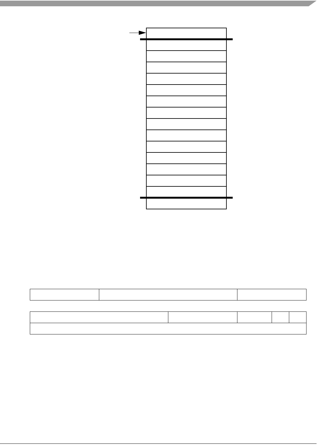
Descriptors
MCF548x Reference Manual, Rev. 3
Freescale Semiconductor 22-57
Figure 22-40. Data Packet Descriptor Format
22.13.1.1 Descriptor Header
Descriptors are created by the host to guide the SEC through required crypto-graphic operations. The
descriptor header defines the operations to be performed, mode for each operation, and internal addressing
used by the controller and channel for internal data movement. Figure 22-41 shows the descriptor header.
.
Table 22-38 defines the header bits.
31 30 29 28 27 26 25 24 23 22 21 20 19 18 17 16
Field PEUSEL PMODE SEUSEL
1514131211109876543210
Field SMODE TYPE — ST DN
Addr Descriptor Pointer + 0x0
Figure 22-41. Descriptor Header
Descriptor Header
Data Field Length 1
Data Field Pointer 1
Data Field Length 2
Data Field Pointer 2
Data Field Length 3
Data Field Pointer 3
Data Field Length 4
Data Field Pointer 4
Data Field Length 5
Data Field Pointer 5
Data Field Length 6
Data Field Pointer 6
Data Field Length 7
Data Field Pointer 7
Next Descriptor Pointer
Descriptor Pointer
+0x04
+0x20
+0x24
+0x28
+0x2C
+0x30
+0x34
+0x38
+0x0C
+0x08
+0x18
+0x1C
+0x14
+0x10
+0x3C

MCF548x Reference Manual, Rev. 3
22-58 Freescale Semiconductor
Table 22-38. Header Bit Definitions
Bits Name Description
31–28 PEUSEL Primary execution unit select. Programs the channel to select a primary EU of a given type. A “No
primary EU selected” or a reserved value in this field will generate an unrecognized header error
condition during processing of the descriptor header.
0x0 No primary EU selected
0x1 AFEU
0x2 DEU
0x3 MDEU
0x4 RNG
0x5 Reserved
0x6 AESU
0x7–0xF Reserved
27–20 PMODE Primary execution unit mode. This data is passed directly to bits 7–0 of the mode register for the
specified EU. See Section 22.14, “ EU Specific Data Packet Descriptors” for descriptions of the
mode registers for each EU.
19–16 SEUSEL Secondary execution unit select. Programs the channel to select a secondary EU of a given type.
The MDEU is the only valid secondary EU. Any value other than ‘MDEU’ or ‘No secondary EU
selected” will generate an unrecognized header error condition during processing of the descriptor
header.
0x0 No secondary EU selected
0x1–0x02 Reserved
0x3 MDEU
0x4-0xF Reserved
Note: If the MDEU is used as a secondary EU, then the primary EU must be DEU, AESU, or AFEU.
All other combinations of primary EU and secondary MDEU processing will generate an
unrecognized header error condition.
15–8 SMODE Secondary execution unit mode. This data is passed directly to bits 7–0 of the mode register for the
specified EU. See Section 22.14, “ EU Specific Data Packet Descriptors” for descriptions of the
mode registers for each EU.
7–4 TYPE Descriptor type. Each type of descriptor determines the following attributes for the corresponding
data length/pointer pairs: the direction of the data flow; which EU is associated with the data; and
which internal EU address is used.
Table 22-39 lists the valid types of descriptors.
3–2 — Reserved. Set to zero

Descriptors
MCF548x Reference Manual, Rev. 3
Freescale Semiconductor 22-59
Table 22-39 shows the permissible values for the descriptor TYPE field in the descriptor header. See
Section 22.13.3, “Descriptor Type Formats” for more information on the data length and pointer pairs
required for each descriptor type.
1 ST Snoop type. Selects which of the two types of available snoop modes applies to the descriptor.
0 Snoop output data mode.
1 Snoop input data mode.
In snoop input data mode, while the bus transaction to write data into the input FIFO of the primary
EU is in progress, the secondary EU (always MDEU) will snoop the same data into its input FIFO.
In snoop output data mode, the secondary EU (always MDEU) will snoop data into its input FIFO
during the bus transaction to read data out of the output FIFO of the primary EU.
When snooping is not performed, this bit is ignored by the SEC crypto-channel.
0 DN Done notification flag. Setting this bit indicates whether to perform notification upon completion of
this descriptor. The notification can take the form of an interrupt or modified header write back or
both depending upon the state of the CCCRn[IE] and CCCRn[WE] control bits.
0 Do not signal DONE upon completion of this descriptor (unless globally programmed to do so via
the master control register).
1 Signal DONE upon completion of this descriptor
The SEC can be programmed to perform DONE notification upon completion of each descriptor,
upon completion of any descriptor, or completion of a chain of descriptors. This bit provides for the
second case.
Table 22-39. Descriptor Types
Value Descriptor Type Notes
0000 aesu_ctr_nonsnoop AESU CTR nonsnoooping
0001 common_nonsnoop_no_afeu Common, nonsnooping,, non-AFEU
0010 hmac_snoop_no_afeu Snooping, HMAC, non-AFEU
0011 non_hmac_snoop_no_afeu Snooping, non-HMAC, non-AFEU
0100 aseu_key expand_output Non-snooping, non HMAC, AESU, expanded key out
0101 common_nonsnoop_afeu Common, nonsnooping, AFEU
0110 hmac_snoop_afeu Snooping, HMAC, AFEU (no context out)
0111 non_hmac_snoop_afeu Snooping, non-HMAC, AFEU
1000 Reserved —
1001 Reserved —
1010 Reserved —
1011 Reserved —
1100 hmac_snoop_aesu_ctr AESU CTR hmac snooping
1101 non_hmac_snoop_aesu_ctr AESU CTR non-hmac snooping
1110 hmac_snoop_afeu_ key_in AFEU Context Out Available
1111 hmac_snoop_afeu_ctx_in AFEU Context Out Available
Table 22-38. Header Bit Definitions (Continued)
Bits Name Description

MCF548x Reference Manual, Rev. 3
22-60 Freescale Semiconductor
22.13.1.2 Descriptor Length and Pointer Fields
The length and pointer fields represent one of seven data length/pointer pairs. Each pair defines a block of
data in system memory. The length field gives the length of the block in bytes. The maximum allowable
number of bytes is 32 Kbytes. A value of zero loaded into the length field indicates that this length/pointer
pair should be skipped and processing should continue with the next pair.
The pointer field contains the address, in ColdFire global memory, of the first byte of the data block.
Transfers from the ColdFire bus with the pointer address set to zero will have the length value written to
the EU, and no data fetched from the memory.
Table 22-40 shows the data packet descriptor length field mapping.
Figure 22-43 shows the descriptor data packet pointer field. The data pointer refers to the address of the
data which the SEC fetches. Data in this case is broadly interpreted to mean keys, context, additional
pointers, or the actual plaintext to be permuted.
Table 22-41 shows the descriptor data packet pointer field mapping.
Table 22-44 shows how the length/pointer pairs should be used with the various descriptor types to load
keys, context, and data into the execution units, and how the required outputs should be unloaded.
31 16 15 0
Field — DATA LENGTH
Addr Descriptor Pointer + 0x4, + 0xC, + 0x14, + 0x1C, + 0x24, + 0x2C, + 0x34
Figure 22-42. Descriptor Data Packet Length Field
Table 22-40. Descriptor Data Packet Length Field Mapping
Bits Name Description
31–16 — Reserved, set to zero.
15–0 DATA
LENGTH
The maximum length this field can be set to 32K bytes. Length fields also indicate the size
of items to be written back to memory upon completion of security processing in the SEC.
31 0
Field DATA FIELD n POINTER
Reset 0
R/W R/W
Figure 22-43. Descriptor Data Packet Pointer Field
Table 22-41. Descriptor Data Packet Pointer Field Mapping
Bits Name Reset Value Description
31–0 DATA FIELD
POINTER
0 The data pointer field contains the address, in global memory, of the first
byte of the data packet for either read or write back. Transfers from the bus
with the pointer address set to zero will be skipped.

Descriptors
MCF548x Reference Manual, Rev. 3
Freescale Semiconductor 22-61
22.13.1.3 Null Fields
On occasion, a descriptor field may not be applicable to the requested service. With seven length/pointer
pairs, it is possible that not all descriptor fields will be required to load the required keys, context, and data.
(Some operations do not require context, others may only need to fetch a small, contiguous block of data.)
Therefore, when processing data packet descriptors, the SEC will skip entirely any pointer that has an
associated length of zero.
22.13.1.4 Next Descriptor Pointer
Following the length/pointer pairs is the ‘Next Descriptor’ field, which contains the pointer to the next
descriptor in memory. Upon completion of processing of the current descriptor, this value, if non-zero, is
used to request a burst read of the next data packet descriptor. This automatic load of the next descriptor
is referred to as descriptor chaining. See Section 22.13.2, “Descriptor Chaining” for more information.
Figure 22-44 displays the next descriptor pointer field.
Table 22-42 describes the descriptor pointer field mapping.
22.13.2 Descriptor Chaining
Descriptor chaining provides a measure of ‘decoupling’ between host CPU activities and the status of the
SEC. Rather than waiting for the SEC to signal DONE, and arbitrating for the bus in order to write directly
to the fetch register in the crypto-channel, the host can simply create new descriptors in memory, and chain
them to descriptors which have not yet been fetched by the SEC by filling the next descriptor pointer field
with the address of the newly created descriptor. Whether or not processing continues automatically
following next-descriptor fetch and whether or not an interrupt is generated depends on the programming
of the Crypto-Channel’s configuration register.
See Section 22.7.1.1, “Crypto-Channel Configuration Registers (CCCRn),” for additional information on
how the SEC can be programmed to signal and act upon completion of a descriptor.
NOTE
It is possible to insert a descriptor into an existing chain; however, great care
must be taken when doing so.
Figure 22-45 shows a conceptual chain, or ‘linked list’ of descriptors.
31 0
Field NDP
Addr Descriptor Pointer + 0x3C
Figure 22-44. Next Descriptor Pointer Field
Table 22-42. Next Descriptor Pointer Field Mapping
Bits Name Description
31–0 NDP Next descriptor pointer. Contains the address, in global memory space, of the next
descriptor to be fetched if descriptor chaining is enabled. This field should be cleared if
chaining is not required.
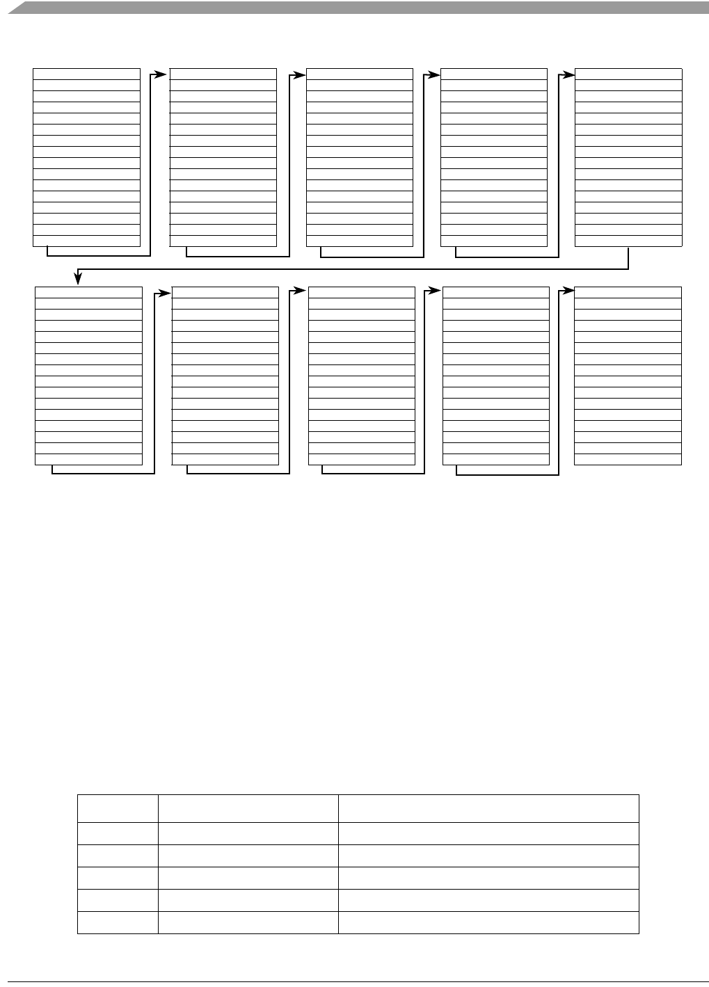
MCF548x Reference Manual, Rev. 3
22-62 Freescale Semiconductor
Figure 22-45. Chain of Descriptors
22.13.3 Descriptor Type Formats
The SEC accepts 12 fixed format descriptors. The descriptor TYPE field in the descriptor header informs
the crypto-channel of the ordering of the inputs and outputs defined by the length/pointer pairs in the
descriptor body. The ordering of inputs and outputs in the length/pointer pairs (as defined by descriptor
type) are shown in Table 22-44.
Table 22-43 shows the permissible values for the TYPE field in the descriptor header.
NOTE
Not all descriptor types are operationally useful. Some exist for test and
debug reasons and to provide flexibility in dealing with evolving security
standards. The cryptographic transforms required by most security
protocols use types 0001 and 0010.
Table 22-43. Descriptor Types
Value Descriptor Type Notes
0000 aesu_ctr_nonsnoop AESU CTR nonsnoooping
0001 common_nonsnoop_no_afeu Common, nonsnooping, non-PKEU, non-AFEU
0010 hmac_snoop_no_afeu Snooping, HMAC, non-AFEU
0011 non_hmac_snoop_no_afeu Snooping, non-HMAC, non-AFEU
0100 aseu_key expand_output Non-snooping, non HMAC, AESU, expanded key out
DPD–DES–CTX_CRYPT
LEN_CTXIN
PTR_CTXIN
LEN_KEY
PTR_KEY
LEN_DATAIN
PTR_DATAIN
LEN_DATAOUT
PTR_DATAOUT
LEN_CTXOUT
PTR_CTXOUT
null length
null pointer
null length
null pointer
PTR_NEXT
DPD–DES–CTX_CRYPT
LEN_CTXIN
PTR_CTXIN
LEN_KEY
PTR_KEY
LEN_DATAIN
PTR_DATAIN
LEN_DATAOUT
PTR_DATAOUT
LEN_CTXOUT
PTR_CTXOUT
null length
null pointer
null length
null pointer
PTR_NEXT
DPD–DES–CTX_CRYPT
LEN_CTXIN
PTR_CTXIN
LEN_KEY
PTR_KEY
LEN_DATAIN
PTR_DATAIN
LEN_DATAOUT
PTR_DATAOUT
LEN_CTXOUT
PTR_CTXOUT
null length
null pointer
null length
null pointer
PTR_NEXT
DPD–DES–CTX_CRYPT
LEN_CTXIN
PTR_CTXIN
LEN_KEY
PTR_KEY
LEN_DATAIN
PTR_DATAIN
LEN_DATAOUT
PTR_DATAOUT
LEN_CTXOUT
PTR_CTXOUT
null length
null pointer
null length
null pointer
PTR_NEXT
DPD–DES–CTX_CRYPT
LEN_CTXIN
PTR_CTXIN
LEN_KEY
PTR_KEY
LEN_DATAIN
PTR_DATAIN
LEN_DATAOUT
PTR_DATAOUT
LEN_CTXOUT
PTR_CTXOUT
null length
null pointer
null length
null pointer
PTR_NEXT
DPD–DES–CTX_CRYPT
LEN_CTXIN
PTR_CTXIN
LEN_KEY
PTR_KEY
LEN_DATAIN
PTR_DATAIN
LEN_DATAOUT
PTR_DATAOUT
LEN_CTXOUT
PTR_CTXOUT
null length
null pointer
null length
null pointer
PTR_NEXT
DPD–DES–CTX_CRYPT
LEN_CTXIN
PTR_CTXIN
LEN_KEY
PTR_KEY
LEN_DATAIN
PTR_DATAIN
LEN_DATAOUT
PTR_DATAOUT
LEN_CTXOUT
PTR_CTXOUT
null length
null pointer
null length
null pointer
PTR_NEXT
DPD–DES–CTX_CRYPT
LEN_CTXIN
PTR_CTXIN
LEN_KEY
PTR_KEY
LEN_DATAIN
PTR_DATAIN
LEN_DATAOUT
PTR_DATAOUT
LEN_CTXOUT
PTR_CTXOUT
null length
null pointer
null length
null pointer
PTR_NEXT
DPD–DES–CTX_CRYPT
LEN_CTXIN
PTR_CTXIN
LEN_KEY
PTR_KEY
LEN_DATAIN
PTR_DATAIN
LEN_DATAOUT
PTR_DATAOUT
LEN_CTXOUT
PTR_CTXOUT
null length
null pointer
null length
null pointer
PTR_NEXT
DPD–DES–CTX_CRYPT
LEN_CTXIN
PTR_CTXIN
LEN_KEY
PTR_KEY
LEN_DATAIN
PTR_DATAIN
LEN_DATAOUT
PTR_DATAOUT
LEN_CTXOUT
PTR_CTXOUT
null length
null pointer
null length
null pointer
PTR_NEXT

Descriptors
MCF548x Reference Manual, Rev. 3
Freescale Semiconductor 22-63
Table 22-44 shows how the length/pointer pairs should be used with the various descriptor types to load
keys, context, and data into the EUs, and how the required outputs should be unloaded.
NOTE
Some of the inputs and outputs will be optional depending on the exact
usage of the descriptor.
0101 common_nonsnoop_afeu Common, nonsnooping, AFEU
0110 hmac_snoop_afeu Snooping, HMAC, AFEU (no context out)
0111 non_hmac_snoop_afeu Snooping, non-HMAC, AFEU
1000 Reserved
1001 Reserved
1010 Reserved
1011 Reserved
1100 hmac_snoop_aesu_ctr AESU CTR hmac snooping
1101 non_hmac_snoop_aesu_ctr AESU CTR non-hmac snooping
1110 hmac_snoop_afeu_ key_in AFEU Context Out Available
1111 hmac_snoop_afeu_ctx_in AFEU Context Out Available
Table 22-44. Descriptor Length/Pointer Mapping
Descriptor
Type L/P 1 L/P 2 L/P 3 L/P 4 L/P 5 L/P 6 L/P 7
0000 Null IV Key Data In Data Out IV Out MAC Out
0001 NULL IV Key Data In Data Out IV Out MAC Out
0010 HMAC Key HMAC Data Key IV Data In Data Out HMAC/Context Out
0011 MD Ctx In IV Key Data In Data Out IV Out MD/Context Out
0100 NULL IV Key Data In Data Out IV Out Key Out via FIFO
0101 NULL IV in via FIFO Key Data In Data Out IV Out via FIFO MD/Context Out
0110 HMAC Key HMAC Data Key IV in via FIFO Data In Data Out HMAC/Context Out
0111 MD Ctx In IV in via FIFO Key Data In Data Out IV Out via FIFO MD/Context Out
1000 —
1001
1010
1011
1100 HMAC Key HMAC Data Key IV Data In Data Out HMAC/Context Out
1101 MD Ctx In IV Key Data In Data Out IV Out MD/Context Out
Table 22-43. Descriptor Types (Continued)
Value Descriptor Type Notes

MCF548x Reference Manual, Rev. 3
22-64 Freescale Semiconductor
22.13.4 Descriptor Classes
The SEC has two general classes of descriptors: dynamic, which refers to a continually changing usage
model, and static, which refers to a relatively unchanging usage of the SEC resources.
22.13.4.1 Dynamic Descriptors
In a typical networking environment, packets from innumerable sessions can arrive randomly. The host
must determine which security association applies to the current packet and encrypt or decrypt without any
knowledge of the security association of the previous or next packet. This situation calls for the use of
dynamic descriptors.
When under dynamic assignment, an EU must be used under the assumption that a different
crypto-channel (with a different context) may have just used the EU and that another crypto-channel (with
yet another context) may use that EU immediately after the current crypto-channel has released the EU.
Therefore, for dynamic-assignment use, there is a set of data packet descriptors defined that sets up the
appropriate context, performs the cipher function, and then saves the context to system memory.
Table 22-45 shows the format for a dynamic descriptor. Since TYPE 0001 and 0010 are the most
commonly used, TYPE 0001 is used for the following examples. The descriptor loads context (IV) and
keys into the EU. Then the input data is read and ciphered and the output is written to system memory.
Finally, the new context is optionally written to system memory so that it can be used as the starting context
for a new descriptor.
1110 HMAC Key HMAC Data Key Data In Data Out IV Out via FIFO HMAC/Context Out
1111 HMAC Key HMAC Data IV Data In Data Out IV Out via FIFO HMAC/Context Out
Table 22-45. Dynamic Descriptor Example
Field Name Value/Type Description
Header 0xXXXX_XX1X TYPE 0001
LEN_1 Length (not used) NULL
PTR_1 Pointer (not used) NULL
LEN_2 IV Length Number of bytes of IV to be written to EU
PTR_2 IV Pointer Address of IV
LEN_3 Key Length Number of bytes of Key to be written to EU
PTR_3 Key Pointer Address of Key
LEN_4 Data In Length Number of bytes to be encrypted/decrypted
PTR_4 Data In Pointer Address of data to be encrypted/decrypted
LEN_5 Data Out Length Bytes to be written (should be equal to length of data in)
PTR_5 Data Out Pointer Address where final data is written
LEN_6 IV Out Length Number of bytes of IV to be written to memory (optional)
Table 22-44. Descriptor Length/Pointer Mapping (Continued)
Descriptor
Type L/P 1 L/P 2 L/P 3 L/P 4 L/P 5 L/P 6 L/P 7

Descriptors
MCF548x Reference Manual, Rev. 3
Freescale Semiconductor 22-65
22.13.4.2 Static Descriptors
Recall that the SEC has five execution units and two crypto-channels. The EUs can be statically assigned
or dedicated to a particular crypto-channel. Certain combinations of EUs can be statically assigned to the
same crypto-channel to facilitate multi-operation security processes, such as IPSec ESP mode. When the
system traffic model permits its use, static assignment can offer significant performance improvements
over dynamic assignment by avoiding key and context switching per packet.
NOTE
There is no mechanism for resetting an EU automatically when statically
assigned, or when assignment is changed from static to dynamic. Therefore,
it is recommended that the drivers always reset an EU prior to removing a
static assignment to prevent the previously used context from polluting
another encryption stream.
Static descriptors split the operations to be performed during a security operation into separate descriptors.
The first descriptor is typically used to set the EU mode, load the key and context, and to optionally
read/permute/write the first block of data. Table 22-46 shows the format for a TYPE 0001 data packet
descriptor that loads a context and key, then encrypts or decrypts the first block of data. The LEN/PTR6
pair is NULL since there is no need to unload the context after the operation completes.
PTR_6 IV Out Pointer Address where IV is to be written (optional)
LEN_7 MAC Out Length NULL
PTR_7 MAC Out Pointer NULL
PTR_NEXT Next Descriptor Pointer Pointer to next data packet descriptor
Table 22-46. First Static Descriptor Example
Field Name Value/Type Description
Header 0xXXXX_XX1X TYPE 0001
LEN_1 Length (not used) NULL
PTR_1 Pointer (not used) NULL
LEN_2 IV Length Number of bytes of IV to be written to EU
PTR_2 IV Pointer Address of IV
LEN_3 Key Length Number of bytes of Key to be written to EU
PTR_3 Key Pointer Address of Key
LEN_4 Data In Length Number of bytes to be encrypted/decrypted
PTR_4 Data In Pointer Address of data to be encrypted/decrypted
LEN_5 Data Out Length Bytes to be written (should be equal to length of data in)
PTR_5 Data Out Pointer Address where final data is written
LEN_6 IV Out Length NULL
Table 22-45. Dynamic Descriptor Example (Continued)
Field Name Value/Type Description

MCF548x Reference Manual, Rev. 3
22-66 Freescale Semiconductor
The middle (and multiple subsequent) descriptors contains length/pointer pairs to the remaining data to be
permuted. Table 22-47 shows the format for a TYPE 0001 data packet descriptor that encrypts or decrypts
a block of data. Since the context and keys were loaded into the EU by a previous data packet descriptor
the LEN/PTR2 and LEN/PTR3 pairs are both NULL.
The final descriptor reads, permutes, and writes the final block of data, and outputs any context that needs
to be preserved for later use. Table 22-48 shows the format for a TYPE 0001 data packet descriptor that
encrypts or decrypts the final block of data and then optionally unloads the context.
PTR_6 IV Out Pointer NULL
LEN_7 MAC Out Length NULL
PTR_7 MAC Out Pointer NULL
PTR_NEXT Next Descriptor Pointer Pointer to next data packet descriptor
Table 22-47. Middle Static Descriptor Example
Field Name Value/Type Description
Header 0xXXXX_XX1X TYPE 0001
LEN_1 Length (not used) NULL
PTR_1 Pointer (not used) NULL
LEN_2 IV Length NULL
PTR_2 IV Pointer NULL
LEN_3 Key Length NULL
PTR_3 Key Pointer NULL
LEN_4 Data In Length Number of bytes to be encrypted/decrypted
PTR_4 Data In Pointer Address of data to be encrypted/decrypted
LEN_5 Data Out Length Bytes to be written (should be equal to length of data in)
PTR_5 Data Out Pointer Address where final data is written
LEN_6 IV Out Length NULL
PTR_6 IV Out Pointer NULL
LEN_7 MAC Out Length NULL
PTR_7 MAC Out Pointer NULL
PTR_NEXT Next Descriptor Pointer Pointer to next data packet descriptor
Table 22-48. Final Static Descriptor Example
Field Name Value/Type Description
Header 0xXXXX_XX1X TYPE 0001
LEN_1 Length (not used) NULL
Table 22-46. First Static Descriptor Example (Continued)
Field Name Value/Type Description

EU Specific Data Packet Descriptors
MCF548x Reference Manual, Rev. 3
Freescale Semiconductor 22-67
Because the key and context are unchanging over multiple packets (or descriptors), the series of short reads
and writes required to set-up and tear down a session are avoided. This savings, along with the
crypto-channel having dedicated execution units, represents a noticeable performance improvement.
22.14 EU Specific Data Packet Descriptors
The following sections describe the data packet descriptor formats used with each of the SEC’s EUs. The
EU mode options (programmable via the PMODE and SMODE fields in the descriptor header) are also
covered.
22.14.1 AFEU Mode Options and Data Packet Descriptors
The AFEU implements an acceleration of a stream cipher compatible with RC4. There are several different
usage modes available.
Table 22-49 describes AFEU mode option fields.
PTR_1 Pointer (not used) NULL
LEN_2 IV Length NULL
PTR_2 IV Pointer NULL
LEN_3 Key Length NULL
PTR_3 Key Pointer NULL
LEN_4 Data In Length Number of bytes to be encrypted/decrypted
PTR_4 Data In Pointer Address of data to be encrypted/decrypted
LEN_5 Data Out Length Bytes to be written (should be equal to length of data in)
PTR_5 Data Out Pointer Address where final data is written
LEN_6 IV Out Length Number of bytes of IV to be written to memory (optional)
PTR_6 IV Out Pointer Address where IV is to be written
LEN_7 MAC Out Length NULL
PTR_7 MAC Out Pointer NULL
PTR_NEXT Next Descriptor Pointer Pointer to next data packet descriptor
76543210
Field —CSDCPP
Reset 0000_0000
Loc PEUMODE/SEUMODE Field in DPD Header
Figure 22-46. AFEU Mode Options
Table 22-48. Final Static Descriptor Example (Continued)
Field Name Value/Type Description

MCF548x Reference Manual, Rev. 3
22-68 Freescale Semiconductor
The AFEU mode bits do not control cryptographic modes, only operational modes. Therefore, the AFEU
only uses actual descriptors, i.e. there is not a representative format that is used with multiple header
values.
22.14.1.1 Dynamically Assigned AFEU
Table 22-50 shows the descriptor format to load a key into the AFEU and perform the initial
context-permutation. Then the input data is ciphered and the context is unloaded.
Table 22-49. AFEU Mode Register Field Descriptions
Bits Name Description
7–3 — Reserved
2 CS Context Source. If set, this causes the context to be moved from the input FIFO into the
S-box prior to starting encryption/decryption. Otherwise, context should be directly written
to the context registers. Context Source is only checked if the prevent permute bit is set.
0 Context not from FIFO
1 Context from input FIFO
1 DC Dump Context. If set, this causes the context to be moved from the S-box to the output
FIFO following assertion AFEU’s done interrupt.
0 Do not dump context
1 After cipher, dump context
0 PP Prevent Permute. Normally, AFEU receives a key and uses that information to randomize
the S-box. If reusing a context from a previous descriptor or if in static assignment mode,
this bit should be set to prevent AFEU from re-performing this permutation step.
0 Perform S-Box permutation
1 Do not permute
Table 22-50. Descriptor for a Dynamically Assigned AFEU Using a Key
Field Name Value/Type Description
Header 0x10200050 Perform permute and dumpt context (TYPE 0101)
LEN_1 Length (not used) NULL
PTR_1 Pointer (not used) NULL
LEN_2 IV Length NULL
PTR_2 IV Pointer NULL
LEN_3 Key Length Number of bytes in key (5–16 bytes)
PTR_3 Key Pointer Address of key to be written into AFEU
LEN_4 Data In Length Number of bytes of data to be ciphered
PTR_4 Data In Pointer Pointer to data to perform cipher upon
LEN_5 Data Out Length Number of bytes of data after ciphering
PTR_5 Data Out Pointer Pointer to location where cipher output is to be written
LEN_6 IV Out Length Number of bytes in context (259 bytes)
PTR_6 IV Out Pointer Location where AFEU context output is to be written

EU Specific Data Packet Descriptors
MCF548x Reference Manual, Rev. 3
Freescale Semiconductor 22-69
Table 22-51 shows the descriptor format to load a previously generated context into the AFEU. Then the
input data is ciphered and the context is unloaded.
22.14.1.2 Statically Assigned AFEU
Statically assigning the AFEU to a particular crypto-channel permits the AFEU to retain state between data
packets. The following descriptors support state-retention. Table 22-52 shows the descriptor format to load
a key into the AFEU and perform the initial context-permutation.
LEN_7 MD Out Length NULL
PTR_7 MD Out Pointer NULL
PTR_NEXT Next Descriptor Pointer Pointer to next data packet descriptor
Table 22-51. Descriptor for a Dynamically Assigned AFEU Using Context
Field Name Value/Type Description
Header 0x1070_0050 Don’t permute, context from FIFO, and dump context
(TYPE 0101)
LEN_1 Length (not used) NULL
PTR_1 Pointer (not used) NULL
LEN_2 IV Length Number of bytes in context (259 bytes)
PTR_2 IV Pointer Address of context to be loaded into AFEU
LEN_3 Key Length NULL
PTR_3 Key Pointer NULL
LEN_4 Data In Length Number of bytes of data to be ciphered.
PTR_4 Data In Pointer Pointer to data to perform cipher upon
LEN_5 Data Out Length Number of bytes of data after ciphering
PTR_5 Data Out Pointer Pointer to location where cipher output is to be written
LEN_6 IV Out Length Number of bytes in context (259 bytes)
PTR_6 IV Out Pointer Address where AFEU context output is to be written
LEN_7 MD Out Length NULL
PTR_7 MD Out Pointer NULL
PTR_NEXT Next Descriptor Pointer Pointer to next data packet descriptor
Table 22-52. First Descriptor for a Statically Assigned AFEU Using a Key
Field Name Value/Type Description
Header 0x1000_0050 Perform permute (TYPE 0101)
LEN_1 Length (not used) NULL
Table 22-50. Descriptor for a Dynamically Assigned AFEU Using a Key (Continued)
Field Name Value/Type Description

MCF548x Reference Manual, Rev. 3
22-70 Freescale Semiconductor
Table 22-53 shows the descriptor format to load a previously generated context into the AFEU.
PTR_1 Pointer (not used) NULL
LEN_2 IV Length NULL
PTR_2 IV Pointer NULL
LEN_3 Key Length Number of bytes in key (5–16 bytes)
PTR_3 Key Pointer Address of key to be written into AFEU
LEN_4 Data In Length NULL
PTR_4 Data In Pointer NULL
LEN_5 Data Out Length NULL
PTR_5 Data Out Pointer NULL
LEN_6 IV Out Length NULL
PTR_6 IV Out Pointer NULL
LEN_7 MAC Out Length NULL
PTR_7 MAC Out Pointer NULL
PTR_NEXT Next Descriptor Pointer Pointer to next data packet descriptor
Table 22-53. First Descriptor for a Statically Assigned AFEU Using a Context
Field Name Value/Type Description
Header 0x1500_0050 Don’t permute; context from FIFO (TYPE 0101)
LEN_1 Length (not used) NULL
PTR_1 Pointer (not used) NULL
LEN_2 IV Length Number of bytes in context (259 bytes)
PTR_2 IV Pointer Address of context to be loaded into AFEU
LEN_3 Key Length NULL
PTR_3 Key Pointer NULL
LEN_4 Data In Length NULL
PTR_4 Data In Pointer NULL
LEN_5 Data Out Length NULL
PTR_5 Data Out Pointer NULL
LEN_6 IV Out Length NULL
PTR_6 IV Out Pointer NULL
LEN_7 MAC Out Length NULL
Table 22-52. First Descriptor for a Statically Assigned AFEU Using a Key (Continued)
Field Name Value/Type Description

EU Specific Data Packet Descriptors
MCF548x Reference Manual, Rev. 3
Freescale Semiconductor 22-71
Table 22-54 shows the descriptor format for the middle descriptor to perform the cipher on a block of data
using a context or key that was loaded into the AFEU using either the first descriptors.
Table 22-55 shows the descriptor format for the final descriptor that unloads the context from the AFEU
into system memory. Architectural implementation details prevent a stand alone unload-context descriptor,
so context unload must always follow ciphering within a single descriptor.
PTR_7 MAC Out Pointer NULL
PTR_NEXT Next Descriptor Pointer Pointer to next data packet descriptor
Table 22-54. Middle Descriptor for a Statically Assigned AFEU
Field Name Value/Type Description
Header 0x1010_0050 Don’t permute, context in AFEU (TYPE 0101)
LEN_1 Length (not used) NULL
PTR_1 Pointer (not used) NULL
LEN_2 IV Length NULL
PTR_2 IV Pointer NULL
LEN_3 Key Length NULL
PTR_3 Key Pointer NULL
LEN_4 Data In Length Number of bytes of data to be ciphered.
PTR_4 Data In Pointer Pointer to data to perform cipher upon
LEN_5 Data Out Length Number of bytes of data after ciphering
PTR_5 Data Out Pointer Pointer to location where cipher output is to be written
LEN_6 IV Out Length NULL
PTR_6 IV Out Pointer NULL
LEN_7 MAC Out Length NULL
PTR_7 MAC Out Pointer NULL
PTR_NEXT Next Descriptor Pointer Pointer to next data packet descriptor
Table 22-55. Final Descriptor for a Statically Assigned AFEU
Field Name Value/Type Description
Header 0x1030_0050 Don’t permute, context in AFEU, and dump context (TYPE 0101)
LEN_1 Length (not used) NULL
PTR_1 Pointer (not used) NULL
LEN_2 IV Length NULL
PTR_2 IV Pointer NULL
Table 22-53. First Descriptor for a Statically Assigned AFEU Using a Context (Continued)
Field Name Value/Type Description

MCF548x Reference Manual, Rev. 3
22-72 Freescale Semiconductor
22.14.2 DEU Mode Options and Data Packet Descriptors
Figure 22-47 shows the DEU options that are programmable via the PMODE field in the descriptor header.
Table 22-56 describes DEU mode register fields.
LEN_3 Key Length NULL
PTR_3 Key Pointer NULL
LEN_4 Data In Length Number of bytes of data to be ciphered.
PTR_4 Data In Pointer Pointer to data to perform cipher upon
LEN_5 Data Out Length Number of bytes of data after ciphering
PTR_5 Data Out Pointer Pointer to location where cipher output is to be written
LEN_6 IV Out Length Number of bytes in context (259 bytes)
PTR_6 IV Out Pointer Address where AFEU context output is to be written
LEN_7 MAC Out Length NULL
PTR_7 MAC Out Pointer NULL
PTR_NEXT Next Descriptor Pointer Pointer to next data packet descriptor
76543210
Field — CETSED
Reset 0000_0000
Loc PMODE Field in DPD Header
Figure 22-47. DEU Mode Options
Table 22-56. DEU Mode Option Field Descriptions
Bits Name Description
0–4 — Reserved
5 CE CBC/ECB. If set, DEU operates in cipher-block-chaining mode. If not set, DEU operates in
electronic codebook mode.
0 ECB mode
1 CBC mode
6 TS Triple/Single DES. If set, DEU operates the Triple DES algorithm; if not set, DEU operates
the single DES algorithm.
0 Single DES (SDES)
1 Triple DES (TDES)
7 ED Encrypt/decrypt. If set, DEU operates the encryption algorithm; if not set, DEU operates
the decryption algorithm.
0 Perform decryption
1 Perform encryption
Table 22-55. Final Descriptor for a Statically Assigned AFEU (Continued)
Field Name Value/Type Description

EU Specific Data Packet Descriptors
MCF548x Reference Manual, Rev. 3
Freescale Semiconductor 22-73
22.14.2.1 Dynamically Assigned DEU
For IPSec processing, it is envisioned that the SEC will need to process small packets of data associated
with many different contexts. This descriptor type is designed to optimize system throughput in a case
where the DEU module is dynamically assigned by the controller to whichever crypto-channel requests it.
Table 22-57 shows a descriptor that loads a key and context (IV) into the DEU, performs the cipher on
data, and writes the result and optional context (IV) to memory.
Table 22-58 lists several different descriptors that use the format shown in Table 22-57.
Table 22-57. Descriptor for a Dynamically Assigned DEU
Field Name Value/Type Description
Header Table 22-58 Header common to several descriptors (TYPE 0001)
LEN_1 Length (not used) NULL
PTR_1 Pointer (not used) NULL
LEN_2 IV Length Number of bytes of IV to be written (always 8) (not used in
ECB mode)
PTR_2 IV Pointer Pointer to context to be written into DEU (not used in ECB
mode)
LEN_3 Key Length Number of bytes in Key (8 for SDES; 16 or 24 or TDES)
PTR_3 Key Pointer Address of Key
LEN_4 Data In Length Number of bytes of data to be ciphered (multiple of 8)
PTR_4 Data In Pointer Address of data to be ciphered
LEN_5 Data Out Length Bytes of output data (should be equal to length of data in)
PTR_5 Data Out Pointer Address to write output data
LEN_6 IV Out Length Number of bytes of output IV to be written (always 8)
(optional)
PTR_6 IV Out Pointer Address where output IV is to be written (optional)
LEN_7 MAC Out Length NULL
PTR_7 MAC Out Pointer NULL
PTR_NEXT Next Descriptor Pointer Pointer to next data packet descriptor
Table 22-58. Typical Header Values for Dynamic DEU Descriptor Format
Header Value E/C S/T E/D
0x20500010 CBC Single DES Encrypt
0x20400010 CBC Single DES Decrypt
0x20700010 CBC Triple DES Encrypt
0x20600010 CBC Triple DES Decrypt
0x20100010 ECB Single DES Encrypt
0x20000010 ECB Single DES Decrypt

MCF548x Reference Manual, Rev. 3
22-74 Freescale Semiconductor
22.14.2.2 Statically Assigned DEU
When statically assigned, it can be assumed that no other crypto-channel will access the DEU in between
descriptors. Therefore, in this usage mode, the context remains within the DEU. The DEU is programmed
with the particular mode of operation at the time of context-load. The following descriptors have been
optimized for encryption/decryption of multiple data packets per context load.
Table 22-59 shows the first descriptor that loads a key and optional context (IV) into the DEU, then
performs the initial cipher.
Table 22-60 lists the specific descriptors that use the format shown in Table 22-59.
0x20300010 ECB Triple DES Encrypt
0x20200010 ECB Triple DES Decrypt
Table 22-59. First Descriptor for a Statically Assigned DEU
Field Name Value/Type Description
Header Table 22-60 Header common to several descriptors (TYPE 0001)
LEN_1 Length (not used) NULL
PTR_1 Pointer (not used) NULL
LEN_2 IV Length Number of bytes of IV to be written (always 8) (optional)
PTR_2 IV Pointer Pointer to context to be written into DEU (optional)
LEN_3 Key Length Number of bytes in Key (8 for SDES; 16 or 24 or TDES)
PTR_3 Key Pointer Address of Key
LEN_4 Data In Length Number of bytes of data to be ciphered (multiple of 8)
PTR_4 Data In Pointer Address of data to be ciphered
LEN_5 Data Out Length Bytes of output data (should be equal to length of data in)
PTR_5 Data Out Pointer Address to write output data
LEN_6 IV Out Length NULL
PTR_6 IV Out Pointer NULL
LEN_7 MAC Out Length NULL
PTR_7 MAC Out Pointer NULL
PTR_NEXT Next Descriptor Pointer Pointer to next data packet descriptor
Table 22-60. Typical Header Values for First Static DEU Descriptor Format
Header Value E/C S/T E/D
0x20500010 CBC Single DES Encrypt
0x20400010 CBC Single DES Decrypt
Table 22-58. Typical Header Values for Dynamic DEU Descriptor Format (Continued)
Header Value E/C S/T E/D

EU Specific Data Packet Descriptors
MCF548x Reference Manual, Rev. 3
Freescale Semiconductor 22-75
Table 22-61 shows the middle descriptor that performs a cipher on data using the key and optional context
(IV) that were loaded into the DEU by the first descriptor.
Table 22-62 lists the specific descriptors that use the format shown in Table 22-61.
0x20700010 CBC Triple DES Encrypt
0x20600010 CBC Triple DES Decrypt
0x20100010 ECB Single DES Encrypt
0x20000010 ECB Single DES Decrypt
0x20300010 ECB Triple DES Encrypt
0x20200010 ECB Triple DES Decrypt
Table 22-61. Middle Descriptor for a Statically Assigned DEU
Field Name Value/Type Description
Header Table 22-62 Header common to several descriptors (TYPE 0001)
LEN_1 Length (not used) NULL
PTR_1 Pointer (not used) NULL
LEN_2 IV Length NULL
PTR_2 IV Pointer NULL
LEN_3 Key Length NULL
PTR_3 Key Pointer NULL
LEN_4 Data In Length Number of bytes of data to be ciphered (multiple of 8)
PTR_4 Data In Pointer Address of data to be ciphered
LEN_5 Data Out Length Bytes of output data (should be equal to length of data in)
PTR_5 Data Out Pointer Address to write output data
LEN_6 IV Out Length NULL
PTR_6 IV Out Pointer NULL
LEN_7 MAC Out Length NULL
PTR_7 MAC Out Pointer NULL
PTR_NEXT Next Descriptor Pointer Pointer to next data packet descriptor
Table 22-62. Typical Header Values for Middle Static DEU Descriptor Format
Header Value E/C S/T E/D
0x20500010 CBC Single DES Encrypt
0x20400010 CBC Single DES Decrypt
0x20700010 CBC Triple DES Encrypt
Table 22-60. Typical Header Values for First Static DEU Descriptor Format (Continued)
Header Value E/C S/T E/D

MCF548x Reference Manual, Rev. 3
22-76 Freescale Semiconductor
Table 22-63 shows the final descriptor that performs a cipher on data using the key and optional context
(IV) that were loaded into the DEU by a previous descriptor, then optionally unloads the context.
Table 22-64 lists the specific descriptors that use the format shown in Table 22-63.
0x20600010 CBC Triple DES Decrypt
0x20100010 ECB Single DES Encrypt
0x20000010 ECB Single DES Decrypt
0x20300010 ECB Triple DES Encrypt
0x20200010 ECB Triple DES Decrypt
Table 22-63. Final Descriptor for a Statically Assigned DEU
Field Name Value/Type Description
Header Table 22-64 Header common to several descriptors (TYPE 0001)
LEN_1 Length (not used) NULL
PTR_1 Pointer (not used) NULL
LEN_2 IV Length NULL
PTR_2 IV Pointer NULL
LEN_3 Key Length NULL
PTR_3 Key Pointer NULL
LEN_4 Data In Length Number of bytes of data to be ciphered (multiple of 8)
PTR_4 Data In Pointer Address of data to be ciphered
LEN_5 Data Out Length Bytes of output data (should be equal to length of data in)
PTR_5 Data Out Pointer Address to write output data
LEN_6 IV Out Length Number of bytes of output IV to be written (always 8)
(optional)
PTR_6 IV Out Pointer Address where output IV is to be written (optional)
LEN_7 MAC Out Length NULL
PTR_7 MAC Out Pointer NULL
PTR_NEXT Next Descriptor Pointer Pointer to next data packet descriptor
Table 22-64. Typical Header Values Final Static DEU Descriptor Format
Header Value E/C S/T E/D
0x20500010 CBC Single DES Encrypt
0x20400010 CBC Single DES Decrypt
0x20700010 CBC Triple DES Encrypt
Table 22-62. Typical Header Values for Middle Static DEU Descriptor Format (Continued)
Header Value E/C S/T E/D

EU Specific Data Packet Descriptors
MCF548x Reference Manual, Rev. 3
Freescale Semiconductor 22-77
22.14.3 MDEU Mode Options and Data Packet Descriptors
The MDEU mode options, shown in Figure 22-48, contains 8 bits which are used to program the MDEU.
The mode options are cleared when the MDEU is reset or re-initialized. Setting a reserved mode bit will
generate a data error. If the mode options are modified during processing, a context error will be generated.
Table 22-65 describes MDEU mode option fields.
0x20600010 CBC Triple DES Decrypt
0x20100010 ECB Single DES Encrypt
0x20000010 ECB Single DES Decrypt
0x20300010 ECB Triple DES Encrypt
0x20200010 ECB Triple DES Decrypt
76543210
Field CONT — INT HMAC PD ALG
Reset 0000_0000
Loc PMODE/SMODE Field in DPD Header
Figure 22-48. MDEU Mode Options
Table 22-65. MDEU Mode Option Field Descriptions
Bits Name Description
7 CONT Continue. Used during HMAC/HASH processing when the data to be hashed is spread
across multiple descriptors.
0 Don’t Continue- operate the MDEU in auto completion mode.
1 Preserve context to operate the MDEU in continuation mode.
6–5 — Reserved
4 INT Initialization. Cause an algorithm-specific initialization of the digest registers. Most
operations will require this bit to be set. Only static operations that are continuing from a
known intermediate hash value would not initialize the registers.
0 Do not initialize
1 Initialize the selected algorithm’s starting registers
3 HMAC HMAC enable. Identifies the hash operation to execute:
0 Perform standard hash
1 Perform HMAC operation. This requires a key and key length information.
Table 22-64. Typical Header Values Final Static DEU Descriptor Format (Continued)
Header Value E/C S/T E/D

MCF548x Reference Manual, Rev. 3
22-78 Freescale Semiconductor
The MDEU implements hardware accelerated hashing of data using MD5, SHA-160, or SHA-256.
Because it supports several different hashing algorithms, there are four representative descriptor formats
supporting more different actual descriptors. The only variation between the actual descriptors are the
values used for the header fields.
22.14.3.1 Recommended Settings for MDEU Mode Register
The most common task that is likely to be executed by means of the MDEU is HMAC generation. HMACs
are used to provide message integrity within a number of security protocols, including IPSec and
SSL/TLS. Table 22-66 shows the recommended MDEU mode register settings for using a single dynamic
descriptor or a chain of descriptors when the MDEU is statically assigned.
22.14.3.2 Dynamically Assigned MDEU
Table 22-67 shows the descriptor format used for a dynamically assigned MDEU. The context is loaded
into the MDEU, input data is fetched and hashed, then the output data and context are written to memory.
Note that the result of a hash is also the context. Because all of the data necessary to calculate the HMAC
in a single dynamic descriptor is available, Initialize and Autopad are set, while Continue is off.
The descriptor header also encodes the descriptor TYPE 0001, which defines the input and output ordering
for “common_nonsnoop_no_afeu.” This is the descriptor type used for most operations which do not
require a secondary EU. Following some null pointers, the context (optional) and the key is loaded (for
HMAC mode), followed by the length and pointer to the data over which the HMAC will be calculated.
The data is brought into the MDEU input FIFO, and when the final byte of data to be hashed has been
processed through the MDEU, the descriptor will cause the MDEU to write the hash to the indicated area
in system memory. The SEC will write the results (16, 20, or 32 bits) to memory. Depending on whether
the packet is inbound or outbound, the host will either insert the most significant bytes (the exact number
of bytes used depends on the security protocol) of the HMAC generated by the SEC into the packet header
2 PD Pad. If set, configures the MDEU to automatically pad partial message blocks.
0 Do not autopad
1 Perform automatic message padding whenever an incomplete message block is
detected.
1–0 ALG Algorithm selection. Determines the algorithm to be used for operations.
00 SHA-160 algorithm (full name for SHA-1)
01 SHA-256 algorithm
10 MD5 algorithm
11 Reserved
Table 22-66. Recommended MDEU Mode Register Settings
Descriptor Type Continue Initialize HMAC Pad
Dynamic Descriptor No Yes Yes Yes
First Static Descriptor Yes Yes Yes No
Middle Static Descriptor Yes No No No
Final Static Descriptor No No Yes Yes
Table 22-65. MDEU Mode Option Field Descriptions (Continued)
Bits Name Description

EU Specific Data Packet Descriptors
MCF548x Reference Manual, Rev. 3
Freescale Semiconductor 22-79
(outbound) or compare the hash generated by the SEC with the hash which was received with the packet
(inbound). If the hashes match, the packet integrity check passes.
Table 22-68 lists several different descriptors that use the format shown in Table 22-67.
22.14.3.3 Statically Assigned MDEU
Table 22-69 shows the first descriptor for a statically assigned MDEU.
Table 22-67. Descriptor for a Dynamically Assigned MDEU
Field Name Value/Type Description
Header see Table 22-68 Header common to several descriptors (TYPE 0001)
LEN_1 Length (not used) NULL
PTR_1 Pointer (not used) NULL
LEN_2 IV Length Number of bytes of IV to be written (optional) (40 bytes)
PTR_2 IV Pointer Pointer to context to be written into MDEU (optional)
LEN_3 Key Length Number of bytes of key (only used for HMAC mode)
PTR_3 Key Pointer Pointer to key (only used for HMAC mode)
LEN_4 Data In Length Number of bytes of data to be hashed
PTR_4 Data In Pointer Pointer to data to perform hash upon
LEN_5 Data Out Length NULL
PTR_5 Data Out Pointer NULL
LEN_6 IV Out Length Number of bytes of data after hashing (16, 20, or 32 for
hash result. 40 bytes for full context including message
length count.)
PTR_6 IV Out Pointer Pointer to location where hash output is to be written
LEN_7 MAC Out Length NULL
PTR_7 MAC Out Pointer NULL
PTR_NEXT Next Descriptor Pointer Pointer to next data packet descriptor
Table 22-68. Typical Header Values for Dynamic MDEU Format
Header Value Algorithm HMAC Pad
0x30500010 SHA256 No Yes
0x30600010 MD5 No Yes
0x30400010 SHA No Yes
0x31D0010 SHA256 Yes Yes
0x31E00010 MD5 Yes Yes
0x31C00010 SHA Yes Yes

MCF548x Reference Manual, Rev. 3
22-80 Freescale Semiconductor
Table 22-70 lists several different descriptors that use the format shown in Table 22-69.
Table 22-71 shows the middle descriptor for a statically assigned MDEU.
Table 22-69. First Descriptor for a Statically Assigned MDEU
Field Name Value/Type Description
Header see Table 22-70 Header common to several descriptors (TYPE 0001)
LEN_1 Length (not used) NULL
PTR_1 Pointer (not used) NULL
LEN_2 IV Length Number of bytes of IV to be written (optional) (40 bytes)
PTR_2 IV Pointer Pointer to context to be written into MDEU (optional)
LEN_3 Key Length Number of bytes of key (only used for HMAC mode)
PTR_3 Key Pointer Pointer to key (only used for HMAC mode)
LEN_4 Data In Length Number of bytes of data to be hashed (64 bytes)
PTR_4 Data In Pointer Pointer to data to perform hash upon
LEN_5 Data Out Length NULL
PTR_5 Data Out Pointer NULL
LEN_6 IV Out Length Number of bytes in intermediate hash output (16, 20, or 32 bytes)
PTR_6 IV Out Pointer Pointer to location where intermediate hash output is to be written
LEN_7 MAC Out Length NULL
PTR_7 MAC Out Pointer NULL
PTR_NEXT Next Descriptor Pointer Pointer to next data packet descriptor
Table 22-70. Typical Header Values for Using First Static MDEU Descriptor Format
Header Value Algorithm HMAC Pad
0x31100010 SHA256 No No
0x31200010 MD5 No No
0x31000010 SHA No No
0x39900010 SHA256 Yes No
0x39A00010 MD5 Yes No
0x39800010 SHA Yes No
Table 22-71. Middle Descriptor for a Statically Assigned MDEU
Field Name Value/Type Description
Header see Table 22-72 Header common to several descriptors (TYPE 0001)
LEN_1 Length (not used) NULL
PTR_1 Pointer (not used) NULL

EU Specific Data Packet Descriptors
MCF548x Reference Manual, Rev. 3
Freescale Semiconductor 22-81
Table 22-72 lists several different descriptors that use the middle descriptor format shown in Table 22-71.
NOTE
For the middle descriptor the HMAC bit should always be cleared, even if
HMAC is the desired final value. Therefor the table below does not include
any HMAC specific settings.
Table 22-73 shows the final descriptor for a statically assigned MDEU.
LEN_2 IV Length Number of bytes in intermediate hash input (16, 20, or 32 bytes)
PTR_2 IV Pointer Pointer to location of intermediate hash input
LEN_3 Key Length Number of bytes of key (only used for HMAC mode)
PTR_3 Key Pointer Pointer to key (only used for HMAC mode)
LEN_4 Data In Length Number of bytes of data to be hashed (64 bytes)
PTR_4 Data In Pointer Pointer to data to perform hash upon
LEN_5 Data Out Length NULL
PTR_5 Data Out Pointer NULL
LEN_6 IV Out Length Number of bytes in intermediate hash output (16, 20, or 32 bytes)
PTR_6 IV Out Pointer Pointer to location where intermediate hash output is to be written
LEN_7 MAC Out Length NULL
PTR_7 MAC Out Pointer NULL
PTR_NEXT Next Descriptor Pointer Pointer to next data packet descriptor
Table 22-72. Typical Header Values for Using Middle Static MDEU Descriptor Format
Header Value Algorithm HMAC Pad
0x38100010 SHA256 No No
0x38200010 MD5 No No
0x38000010 SHA No No
Table 22-73. Final Descriptor for a Statically Assigned MDEU
Field Name Value/Type Description
Header see Table 22-74 Header common to several descriptors (TYPE 0001)
LEN_1 Length (not used) NULL
PTR_1 Pointer (not used) NULL
LEN_2 IV Length Number of bytes in intermediate hash (16, 20, or 32 bytes)
PTR_2 IV Pointer Pointer to location of intermediate hash
LEN_3 Key Length Number of bytes of key (only used for HMAC mode)
Table 22-71. Middle Descriptor for a Statically Assigned MDEU (Continued)
Field Name Value/Type Description

MCF548x Reference Manual, Rev. 3
22-82 Freescale Semiconductor
Table 22-74 lists several different descriptors that use the final MDEU descriptor format shown in
Table 22-73.
22.14.4 RNG Data Packet Descriptors
There is one RNG-specific data packet descriptor. It causes a read of the RNG’s output FIFO and then
writes the specified number of random bytes into external memory.
NOTE
There RNG EU does not contain any user writable mode options, so it is not
defined here. The PMODE field in the header should always be ‘0’ for RNG
data packet descriptors.
PTR_3 Key Pointer Pointer to key (only used for HMAC mode)
LEN_4 Data In Length Number of bytes of data to be hashed
PTR_4 Data In Pointer Pointer to data to perform hash upon
LEN_5 Data Out Length NULL
PTR_5 Data Out Pointer NULL
LEN_6 IV Out Length Number of bytes of data after hashing (16, 20, or 32 bytes)
PTR_6 IV Out Pointer Pointer to location where hash output is to be written
LEN_7 MAC Out Length NULL
PTR_7 MAC Out Pointer NULL
PTR_NEXT Next Descriptor Pointer Pointer to next data packet descriptor
Table 22-74. Typical Header Values for Using Final Static MDEU Descriptor Format
Header Value Algorithm HMAC Pad
0x30500010 SHA256 No Yes
0x30600010 MD5 No Yes
0x30400010 SHA No Yes
0x30D00010 SHA256 Yes Yes
0x30E00010 MD5 Yes Yes
0x30C00010 SHA Yes Yes
Table 22-75. RNG Descriptor Format
Field Name Value/Type Description
Header 0x4000_0010 RNG descriptor (TYPE 0001)
LEN_1 Length (not used) NULL
PTR_1 Pointer (not used) NULL
Table 22-73. Final Descriptor for a Statically Assigned MDEU (Continued)
Field Name Value/Type Description

EU Specific Data Packet Descriptors
MCF548x Reference Manual, Rev. 3
Freescale Semiconductor 22-83
22.14.5 AESU Mode Options and Data Packet Descriptors
The AESU mode register contains three bits which are used to program the AESU. The mode register is
cleared when the AESU is reset or re-initialized. Setting a reserved mode bit will generate a data error. If
the mode register is modified during processing, a context error will be generated.
Figure 22-49 shows the AESU options that are programmable via the PMODE field in the descriptor
header.
Table 22-76 describes AESU mode register fields.
LEN_2 IV Length NULL
PTR_2 IV Pointer NULL
LEN_3 Key Length NULL
PTR_3 Key Pointer NULL
LEN_4 Data In Length NULL
PTR_4 Data In Pointer NULL
LEN_5 Data Out Length Number of random bytes to be written (multiple of 4)
PTR_5 Data Out Pointer Address where random numbers are written
LEN_6 IV Out Length NULL
PTR_6 IV Out Pointer NULL
LEN_7 MAC Out Length NULL
PTR_7 MAC Out Pointer NULL
PTR_NEXT Next Descriptor Pointer Pointer to next data packet descriptor
76543210
Field ECM — FM IM — CM ED
Reset 0000_0000
Loc PMODE Field in DPD Header
Figure 22-49. AESU Mode Options
Table 22-76. AESU Mode Register Field Descriptions
Bits Name Description
7 ECM Extend Cipher Mode. Used in combination with the cipher mode (CM field) to define the mode
of AES operation.
0 No Cipher Mode extension in use, Cipher Mode selected by CM values
1 Extended Cipher Mode. Indicates AES-Counter Mode with CBC-MAC (AES-CCM) is in use.
Note: CM must be set to 00 when Extend Cipher Mode is set, otherwise an error will be
generated.
6 — Reserved, should be cleared.
Table 22-75. RNG Descriptor Format (Continued)
Field Name Value/Type Description

MCF548x Reference Manual, Rev. 3
22-84 Freescale Semiconductor
22.14.5.1 Dynamically Assigned AESU
Table 22-77 shows a descriptor for a dynamically assigned AESU. The descriptor loads a key into the
AESU, performs the cipher on data, and writes the result and optional context (IV) to memory.
5 FM Final MAC. Processes final message block and generates final MAC tag at end of message
processing (OCB and CCM mode only)
0 Do not generate final MAC tag
1 Generate final MAC tag after CCM processing is complete.
4 IM Initialize MAC. Initializes AESU for new message (CCM mode only)
0 Do not initialize (context will be loaded by host)
1 Initialize new message with nonce
3 — Reserved, should be cleared.
2–1 CM Cipher Mode. Controls which cipher mode the AESU will use in processing:
00 ECB -Electronic Codebook mode.
01 CBC- Cipher Block Chaining mode.
10 Reserved
11 CTR- Counter Mode.
Note: CM must be set to 00 when Extend Cipher Mode (Bit 0) is set, otherwise an error will be
generated.
0 ED Encrypt/Decrypt. If set, AESU operates the encryption algorithm; if not set, AESU operates the
decryption algorithm.
Note: This bit is ignored if CM is set to “11” - CTR Mode.
0 Perform decryption
1 Perform encryption
Table 22-77. Descriptor for a Dynamically Assigned AESU
Field Name Value/Type Description
Header Table 22-61 Header common to several descriptors (TYPE 0001)
LEN_1 Length (not used) NULL
PTR_1 Pointer (not used) NULL
LEN_2 IV Length Number of bytes in input IV (56 bytes) (optional)
PTR_2 IV Pointer Address of input IV (optional)
LEN_3 Key Length Number of bytes in Key (16, 24, or 32 bytes)
PTR_3 Key Pointer Address of Key
LEN_4 Data In Length Number of bytes of data to be ciphered (multiple of 16)
PTR_4 Data In Pointer Address of data to be ciphered
LEN_5 Data Out Length Bytes of output data (should be equal to length of data in)
PTR_5 Data Out Pointer Address to write output data
LEN_6 IV Out Length Number of bytes of output IV to be written (56 bytes) (optional)
Table 22-76. AESU Mode Register Field Descriptions (Continued)
Bits Name Description

EU Specific Data Packet Descriptors
MCF548x Reference Manual, Rev. 3
Freescale Semiconductor 22-85
Table 22-78 lists several different descriptors that use the format shown in Table 22-77.
22.14.5.2 Statically Assigned AESU
Table 22-69 shows the first descriptor for a statically assigned AESU.
PTR_6 IV Out Pointer Address where output IV is to be written (optional)
LEN_7 MAC Out Length NULL
PTR_7 MAC Out Pointer NULL
PTR_NEXT Next Descriptor Pointer Pointer to next data packet descriptor
Table 22-78. Typical Header Values for Dynamic AESU Format
Header Value Mode E/D
0x6030010 CBC Encrypt
0x60200010 CBC Decrypt
0x6010010 ECB Encrypt
0x60000010 ECB Decrypt
0x60600010 CTR —
Table 22-79. First Descriptor for a Statically Assigned AESU
Field Name Value/Type Description
Header see Table 22-80 Header common to several descriptors (TYPE 0001)
LEN_1 Length (not used) NULL
PTR_1 Pointer (not used) NULL
LEN_2 IV Length Number of bytes in input IV (56 bytes) (optional)
PTR_2 IV Pointer Address of input IV (optional)
LEN_3 Key Length Number of bytes in Key (16, 24, or 32 bytes)
PTR_3 Key Pointer Address of Key
LEN_4 Data In Length Number of bytes of data to be ciphered (multiple of 16)
PTR_4 Data In Pointer Address of data to be ciphered
LEN_5 Data Out Length Bytes of output data (should be equal to length of data in)
PTR_5 Data Out Pointer Address to write output data
LEN_6 IV Out Length NULL
PTR_6 IV Out Pointer NULL
LEN_7 MAC Out Length NULL
Table 22-77. Descriptor for a Dynamically Assigned AESU (Continued)
Field Name Value/Type Description

MCF548x Reference Manual, Rev. 3
22-86 Freescale Semiconductor
Table 22-80 lists several different descriptors that use the format shown in Table 22-79.
Table 22-81 shows the middle descriptor for a statically assigned AESU.
Table 22-82 lists several different descriptors that use the middle descriptor format shown in Table 22-81.
PTR_7 MAC Out Pointer NULL
PTR_NEXT Next Descriptor Pointer Pointer to next data packet descriptor
Table 22-80. Typical Header Values for Using First Static AESU Descriptor Format
Header Value Mode E/D
0x6030010 CBC Encrypt
0x60200010 CBC Decrypt
0x6010010 ECB Encrypt
0x60000010 ECB Decrypt
0x60600010 CTR —
Table 22-81. Middle Descriptor for a Statically Assigned AESU
Field Name Value/Type Description
Header see Table 22-82 Header common to several descriptors (TYPE 0001)
LEN_1 Length (not used) NULL
PTR_1 Pointer (not used) NULL
LEN_2 IV Length NULL
PTR_2 IV Pointer NULL
LEN_3 Key Length NULL
PTR_3 Key Pointer NULL
LEN_4 Data In Length Number of bytes of data to be ciphered (multiple of 16)
PTR_4 Data In Pointer Address of data to be ciphered
LEN_5 Data Out Length Bytes of output data (should be equal to length of data in)
PTR_5 Data Out Pointer Address to write output data
LEN_6 IV Out Length NULL
PTR_6 IV Out Pointer NULL
LEN_7 MAC Out Length NULL
PTR_7 MAC Out Pointer NULL
PTR_NEXT Next Descriptor Pointer Pointer to next data packet descriptor
Table 22-79. First Descriptor for a Statically Assigned AESU (Continued)
Field Name Value/Type Description

EU Specific Data Packet Descriptors
MCF548x Reference Manual, Rev. 3
Freescale Semiconductor 22-87
Table 22-83 shows the final descriptor for a statically assigned AESU.
Table 22-84 lists several different descriptors that use the middle descriptor format shown in Table 22-83.
Table 22-82. Typical Header Values for Using Middle Static AESU Descriptor Format
Header Value Mode E/D
0x6030010 CBC Encrypt
0x60200010 CBC Decrypt
0x6010010 ECB Encrypt
0x60000010 ECB Decrypt
0x60600010 CTR —
Table 22-83. Final Descriptor for a Statically Assigned AESU
Field Name Value/Type Description
Header see Table 22-84 Header common to several descriptors (TYPE 0001)
LEN_1 Length (not used) NULL
PTR_1 Pointer (not used) NULL
LEN_2 IV Length NULL
PTR_2 IV Pointer NULL
LEN_3 Key Length NULL
PTR_3 Key Pointer NULL
LEN_4 Data In Length Number of bytes of data to be ciphered (multiple of 16)
PTR_4 Data In Pointer Address of data to be ciphered
LEN_5 Data Out Length Bytes of output data (should be equal to length of data in)
PTR_5 Data Out Pointer Address to write output data
LEN_6 IV Out Length Number of bytes of output IV to be written (56 bytes) (optional)
PTR_6 IV Out Pointer Address where output IV is to be written (optional)
LEN_7 MAC Out Length NULL
PTR_7 MAC Out Pointer NULL
PTR_NEXT Next Descriptor Pointer Pointer to next data packet descriptor
Table 22-84. Typical Header Values for Using Final Static AESU Descriptor Format
Header Value Mode E/D
0x6030010 CBC Encrypt
0x60200010 CBC Decrypt
0x6010010 ECB Encrypt

MCF548x Reference Manual, Rev. 3
22-88 Freescale Semiconductor
22.14.5.3 AESU-CCM Mode Descriptor
The SEC supports single pass, single descriptor AES-CCM processing for generic
authenticate-and-encrypt block cipher. Table 22-85 shows a the descriptor format used for AES-CCM in
encryption mode. The descriptor loads a key and context (IV) into the AESU, performs the cipher on data,
and writes the result and context to memory.
In order to use this descriptor format the correct ordering for the context in and context out must be used.
Table 22-86 shows the format used for the context input for AES-CCM.
0x60000010 ECB Decrypt
0x60600010 CTR —
Table 22-85. Descriptor for a AES-CCM Encryption
Field Name Value/Type Description
Header 0x6B100010 Header common to several descriptors (TYPE 0001)
LEN_1 Length (not used) NULL
PTR_1 Pointer (not used) NULL
LEN_2 IV Length Number of bytes in IV (always 56 bytes)
PTR_2 IV Pointer Address of IV
LEN_3 Key Length Number of bytes in Key (16 bytes)
PTR_3 Key Pointer Address of Key
LEN_4 Data In Length Number of bytes of data to be ciphered (39 bytes)
PTR_4 Data In Pointer Address of data to be ciphered
LEN_5 Data Out Length Bytes of output data (24 bytes)
PTR_5 Data Out Pointer Address to write output data
LEN_6 IV Out Length Number of bytes of output IV to be written (24 or 32 bytes)
PTR_6 IV Out Pointer Address where output IV is to be written
LEN_7 MAC Out Length NULL
PTR_7 MAC Out Pointer NULL
PTR_NEXT Next Descriptor Pointer Pointer to next data packet descriptor
Table 22-84. Typical Header Values for Using Final Static AESU Descriptor Format (Continued)
Header Value Mode E/D

EU Specific Data Packet Descriptors
MCF548x Reference Manual, Rev. 3
Freescale Semiconductor 22-89
Table 22-87 shows the format used for the context output for AES-CCM.
Table 22-88 shows a the descriptor format used for AES-CCM in encryption mode. The descriptor loads
a key and context (IV) into the AESU, performs the cipher on data, and writes the result and context to
memory.
Table 22-86. AES-CCM Encryption Context Input Format
Offset from
Input Context
Base Address
Field Length Description
0x0 IV 16 bytes This is the session specific IV parameter
0x10 NULL 16 bytes These 16 bytes are loaded with zeroes to serve as a
placeholder
0x20 Counter 16 bytes The counter is a second session specific parameter
similar to the IV.
0x30 Counter
modulus
8 bytes Always 8 for 802.11, but can very in other protocols.
Table 22-87. AES-CCM Encryption Context Output Format
Offset from
Output Context
Base Address
Field Length Description
0x0 — 16 bytes This can be discarded
0x10 Encrypted MAC 8 bytes This is the encrypted MAC to be appended to the
frame prior to transmission.
0x18 Encrypted MAC
(cont.)
8 bytes If the MAC is larger than 8 bytes, this is the
continuation of the encrypted MAC.
Table 22-88. Descriptor for a AES-CCM Decryption
Field Name Value/Type Description
Header 0x6B000010 Header common to several descriptors (TYPE 0001)
LEN_1 Length (not used) NULL
PTR_1 Pointer (not used) NULL
LEN_2 IV Length Number of bytes in IV (always 56 bytes)
PTR_2 IV Pointer Address of IV
LEN_3 Key Length Number of bytes in Key (16 bytes)
PTR_3 Key Pointer Address of Key
LEN_4 Data In Length Number of bytes of data to be ciphered (39 bytes)
PTR_4 Data In Pointer Address of data to be ciphered
LEN_5 Data Out Length Bytes of output data (24 bytes)
PTR_5 Data Out Pointer Address to write output data

MCF548x Reference Manual, Rev. 3
22-90 Freescale Semiconductor
Table 22-89 shows the format used for the context input for AES-CCM.
Table 22-87 shows the format used for the context output for AES-CCM.
22.14.6 Multi-Function Data Packet Descriptors
The SEC supports a limited subset of multi-function descriptors. In particular, the SEC supports chaining
either DEU, AESU, or AFEU compatible outputs to the MDEU input. Further, the SEC can be configured
LEN_6 IV Out Length Number of bytes of output IV to be written (24 or 32 bytes)
PTR_6 IV Out Pointer Address where output IV is to be written
LEN_7 MAC Out Length NULL
PTR_7 MAC Out Pointer NULL
PTR_NEXT Next Descriptor Pointer Pointer to next data packet descriptor
Table 22-89. AES-CCM Decryption Context Input Format
Offset from
Input Context
Base Address
Field Length Description
0x0 IV 16 bytes This is the session specific IV parameter
0x10 Encrypted MAC 8 bytes These 8 bytes are loaded with the encrypted MAC
from the inbound frame.
0x18 Encrypted MAC
(cont.)
8 bytes These 8 bytes can be used for the continuation of the
encrypted MAC if it is larger than 8 bytes. Otherwise
this field should be filled with zeroes.
0x20 Counter 16 bytes The counter is a second session specific parameter
similar to the IV.
0x30 Counter
modulus
8 bytes Always 8 for 802.11, but can very in other protocols.
Table 22-90. AES-CCM Decryption Context Output Format
Offset from
Output Context
Base Address
Field Length Description
0x0 MAC Tag 8 bytes The MAC Tag is compared to the decrypted MAC
0x8 MAC Tag (cont.) 16 bytes Continuation of the MAC Tag if it is larger than 8 bytes.
Typically this field will be all zeroes.
0x10 Decrypted MAC 8 bytes Compared to the MAC tag to determine if the frame
passes its integrity check.
0x18 Decrypted MAC
(cont.)
8 bytes If the MAC is larger than 16 bytes, this is the
continuation of the decrypted MAC.
Table 22-88. Descriptor for a AES-CCM Decryption (Continued)
Field Name Value/Type Description
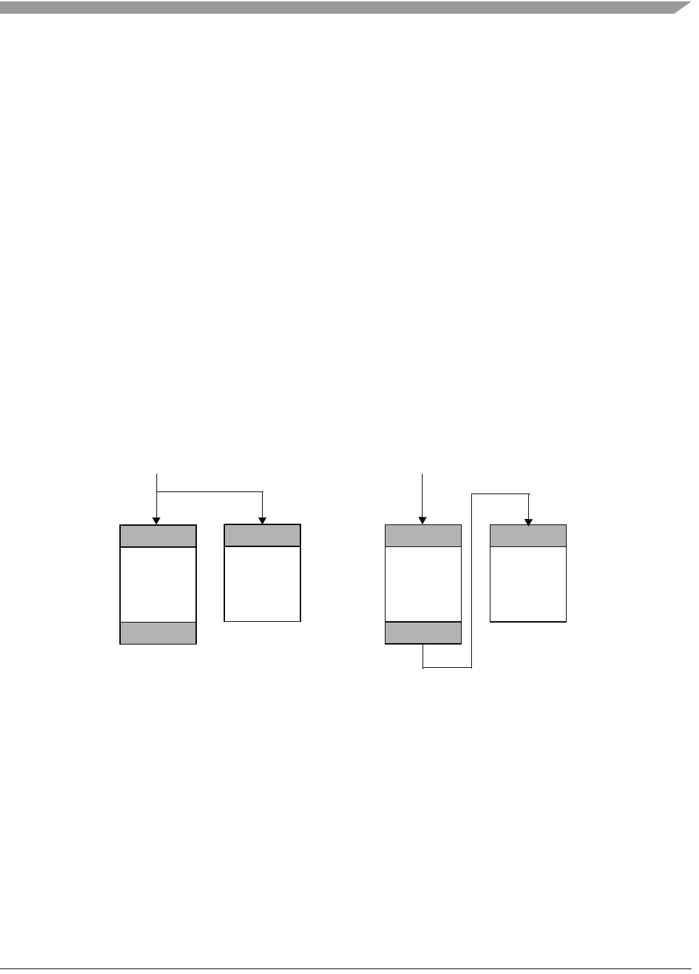
EU Specific Data Packet Descriptors
MCF548x Reference Manual, Rev. 3
Freescale Semiconductor 22-91
such that the same data read into the DEU, AESU, or AFEU modules can be simultaneously directed to
the MDEU module.
22.14.6.1 Snooping
As shown in Figure 22-41, the ST bit in the descriptor header controls the type of snooping which must
occur between the primary and secondary EU. The rationale of in-snooping vs. out-snooping is found in
security protocols which perform both encryption and integrity checking, such as IPSec.
Upon transmission of an IPSec ESP packet, the encapsulator must encrypt the packet payload, then
calculate an HMAC over the header plus encrypted payload. Because the MDEU cannot generate the
HMAC without the output of the primary EU (the one performing the encryption, typically the DEU or
AESU), the MDEU must out-snoop.
Upon receiving an IPSec packet, the decapsulator must calculate the HMAC over the encrypted portion or
the packet prior to decryption. In this case in-snooping would be used. This allows the MEDU to source
its data from the input FIFO of the primary EU without waiting for the primary EU to finish its task.
NOTE
Slightly different portions of an IPSec packet would pass through the
primary and secondary EUs in both the in-snooping and out-snooping cases.
These offsets are dealt with by providing different starting pointers and byte
lengths to the channel in the body of the descriptor.
Figure 22-50 illustrates in-snooping and out-snooping.
Figure 22-50. Snooping Example
22.14.6.2 Dynamic Multi-Function Descriptor Formats
Table 22-91 shows the representative descriptor used for multi-function encryption such as inbound IPSec
ESP. The descriptor header encodes to select the DEU or AESU as the primary EU, and the MDEU for the
secondary EU. Because all the data necessary to calculate the HMAC in a single dynamic descriptor is
available, initialize and autopad are set, while continue is cleared in the SMODE field.
The descriptor header also encodes the descriptor type 0010, which defines the input and output ordering
for “hmac_snoop_no_afeu.” The HMAC key is loaded first, followed by the length and pointer to the data
over which the HMAC will be calculated. The DEU/AESU key is loaded next, followed by the context
(IV). The number of bytes to be ciphered and starting address will be an offset of the number of bytes being
HMAC’d. The data to be decrypted and HMAC’d is only brought in the SEC a single time, with the
In FIFO
Out FIFO
DEU
In FIFO
Out FIFO
DEU
In-Snooping Out-Snooping
In FIFO
MDEU
In FIFO
MDEU

MCF548x Reference Manual, Rev. 3
22-92 Freescale Semiconductor
DEU/AESU and MDEU only reading the portion that matches the starting address and byte length in the
length/pointer fields corresponding to their data of interest.
Ciphertext is brought into the DEU/AESU input FIFO, with the MDEU in-snooping the portion of the data
it has been told to process. As the decryption continues, the plaintext fills the DEU/AEU output FIFO, and
this data is written back to system memory as needed. When the final byte of data to be HMAC’d has been
processed through the MDEU, the descriptor will cause the MDEU to write the HMAC to the indicated
area in system memory. Software will compare the most significant bytes of the HMAC generated by the
SEC with the HMAC which was received with the in-bound packet (the exact number of bytes compared
depend on the security protocol used). If the HMACs match, the integrity check passes.
Table 22-92 lists typical DEU/HMAC multi-function descriptor header values.
Table 22-91. Descriptor for Dynamic Multi-Function Decryption
Field Name Value/Type Description
Header Table 22-92 Header common to several descriptors (TYPE 0010)
LEN_1 HMAC Key Length Number of bytes in HMAC Key
PTR_1 HMAC Key Pointer Address of HMAC Key
LEN_2 HMAC Data Length Number of bytes to be HMAC’d
PTR_2 HMAC Data Pointer Address of data to be HMAC’d
LEN_3 Key Length Number of bytes in Key (8, 16, 24, or 32 bytes)
PTR_3 Key Pointer Address of Key
LEN_4 IV Length Number of bytes in IV (8, 24, or 56)
PTR_4 IV Pointer Address of IV
LEN_5 Data In Length Bytes of ciphertext to be decrypted
PTR_5 Data In Pointer Address of ciphertext to be decrypted
LEN_6 Data Out Length Bytes of output data (should be equal to length of data in)
PTR_6 Data Out Pointer Address where output data is to be written
LEN_7 HMAC Out Length Number of bytes HMAC output (16, 20 or 32 bytes)
PTR_7 HMAC Out Pointer Address where hash output is to be written
PTR_NEXT Next Descriptor Pointer Pointer to next data packet descriptor
Table 22-92. Typical Header Values for Dynamic Multi-Function DEU Descriptors
Header Value E/C S/T E/D Algorithm HMAC Pad
0x20031D22 ECB Single DES Decrypt SHA256 Yes Yes
0x20031E22 ECB Single DES Decrypt MD5 Yes Yes
0x20031C22 ECB Single DES Decrypt SHA Yes Yes
0x20431D22 ECB Triple DES Decrypt SHA256 Yes Yes
0x20431E22 ECB Triple DES Decrypt MD5 Yes Yes
0x20431C22 ECB Triple DES Decrypt SHA Yes Yes

EU Specific Data Packet Descriptors
MCF548x Reference Manual, Rev. 3
Freescale Semiconductor 22-93
Table 22-93 lists typical AESU/HMAC multi-function descriptor header values.
Table 22-94 shows the representative descriptor used for multi-function encryption such as outbound
IPSec ESP. The descriptor header encodes to select the DEU or AESU as the primary EU, and the MDEU
for the secondary EU. Because all the data necessary to calculate the HMAC in a single dynamic descriptor
is available, initialize and autopad are set, while continue is cleared in the SMODE field.
The descriptor header also encodes the descriptor type 0010, which defines the input and output ordering
for “hmac_snoop_no_afeu.” The HMAC key is loaded first, followed by the length and pointer to the data
over which the HMAC will be calculated. The DEU/AESU key is loaded next, followed by the context
(IV). The number of bytes to be ciphered and starting address will be an offset of the number of bytes being
HMAC’d. The data to be decrypted and HMAC’d is only brought in the SEC a single time, with the
DEU/AESU and MDEU only reading the portion that matches the starting address and byte length in the
length/pointer fields corresponding to their data of interest.
Plaintext is brought into the DEU/AESU input FIFO, with the MDEU out-snooping the portion of the data
it has been told to process. As the encryption continues, the ciphertext fills the DEU/AEU output FIFO,
and this data is written back to system memory as needed. When the final byte of data to be HMAC’d has
been processed through the MDEU, the descriptor will cause the MDEU to write the HMAC to the
indicated area in system memory. Software will append the most significant bytes of the HMAC generated
by the SEC to the packet as the authentication trailer. Common practice in IPSec ESP with TDES-CBC is
to use the last 8 bytes of the ciphertext as the IV for the next packet. If this is the case, software should
0x20231D22 CBC Single DES Decrypt SHA256 Yes Yes
0x20231E22 CBC Single DES Decrypt MD5 Yes Yes
0x20231C22 CBC Single DES Decrypt SHA Yes Yes
0x20631D22 CBC Triple DES Decrypt SHA256 Yes Yes
0x20631E22 CBC Triple DES Decrypt MD5 Yes Yes
0x20631C22 CBC Triple DES Decrypt SHA Yes Yes
Table 22-93. Typical Header Values for Dynamic Multi-Function AESU Descriptors
Header Value Mode E/D Algorithm HMAC Pad
0x60831D22 ECB Decrypt SHA256 Yes Yes
0x60831E22 ECB Decrypt MD5 Yes Yes
0x60831C22 ECB Decrypt SHA Yes Yes
0x60A31D22 CBC Decrypt SHA256 Yes Yes
0x60A31E22 CBC Decrypt MD5 Yes Yes
0x60A31C22 CBC Decrypt SHA Yes Yes
0x60E31D22 CTR — SHA256 Yes Yes
0x60E31E22 CTR — MD5 Yes Yes
0x60E31C22 CTR — SHA Yes Yes
Table 22-92. Typical Header Values for Dynamic Multi-Function DEU Descriptors (Continued)
Header Value E/C S/T E/D Algorithm HMAC Pad

MCF548x Reference Manual, Rev. 3
22-94 Freescale Semiconductor
copy the last 8 bytes of the ciphertext to the Security Association Database Entry for this particular session
before transmitting the packet.
Table 22-95 lists typical DEU/HMAC multi-function descriptor header values.
Table 22-94. Descriptor for Dynamic Multi-Function Encryption
Field Name Value/Type Description
Header Table 22-95 Header common to several descriptors (TYPE 0010)
LEN_1 HMAC Key Length Number of bytes in HMAC Key
PTR_1 HMAC Key Pointer Address of HMAC Key
LEN_2 HMAC Data Length Number of bytes to be HMAC’d
PTR_2 HMAC Data Pointer Address of data to be HMAC’d
LEN_3 Key Length Number of bytes in Key (8, 16, 24, or 32 bytes)
PTR_3 Key Pointer Address of Key
LEN_4 IV Length Number of bytes in IV (8, 24, or 56)
PTR_4 IV Pointer Address of IV
LEN_5 Data In Length Bytes of plaintext to be encrypted
PTR_5 Data In Pointer Address of plaintext to be encrypted
LEN_6 Data Out Length Bytes of output data (should be equal to length of data in)
PTR_6 Data Out Pointer Address where output data is to be written
LEN_7 HMAC Out Length Number of bytes HMAC output (16, 20 or 32 bytes)
PTR_7 HMAC Out Pointer Address where hash output is to be written
PTR_NEXT Next Descriptor Pointer Pointer to next data packet descriptor
Table 22-95. Typical Header Values for Dynamic Multi-Function DEU Descriptors
Header Value E/C S/T E/D Algorithm HMAC Pad
0x20131D20 ECB Single DES Encrypt SHA256 Yes Yes
0x20131E20 ECB Single DES Encrypt MD5 Yes Yes
0x20131C20 ECB Single DES Encrypt SHA Yes Yes
0x20531D20 ECB Triple DES Encrypt SHA256 Yes Yes
0x20531E20 ECB Triple DES Encrypt MD5 Yes Yes
0x20531C20 ECB Triple DES Encrypt SHA Yes Yes
0x20331D20 CBC Single DES Encrypt SHA256 Yes Yes
0x20331E20 CBC Single DES Encrypt MD5 Yes Yes
0x20331C20 CBC Single DES Encrypt SHA Yes Yes
0x20731D20 CBC Triple DES Encrypt SHA256 Yes Yes

EU Specific Data Packet Descriptors
MCF548x Reference Manual, Rev. 3
Freescale Semiconductor 22-95
Table 22-96 lists typical AESU/HMAC multi-function descriptor header values.
22.14.6.3 Static Multi-Function Descriptor Formats
This example is designed to contrast the dynamic descriptors shown in Section 22.14.6.2, “Dynamic
Multi-Function Descriptor Formats.” For whatever reason, the data to be decrypted/encrypted and
authenticated is not available in a single contiguous block, or the total data size is larger than 32 Kbytes.
The user must statically assign a DEU/AESU and MDEU to a channel before launching this descriptor
chain.
Table 22-97 shows the representative descriptor format for the first descriptor in a statically assigned
multi-function operation descriptor chain. The first descriptor header encodes to select the DEU or AESU
as the primary EU, and the MDEU for the secondary EU. Because all the data necessary to calculate the
HMAC in a single dynamic descriptor is not available, initialize and continue are set and the autopad bit
is cleared in the SMODE field.
The descriptor header also encodes the descriptor type 0010, which defines the input and output ordering
for “hmac_snoop_no_afeu.” The HMAC key is loaded first, followed by the length and pointer to the data
over which the initial HMAC will be calculated. The DEU/AESU key is loaded next, followed by the
context (IV). The number of bytes to be ciphered and starting address will be an offset of the number of
bytes being HMAC’d. The data to be decrypted and HMAC’d is only brought in the SEC a single time,
with the DEU/AESU and MDEU only reading the portion that matches the starting address and byte length
in the length/pointer fields corresponding to their data of interest.
Input data is brought into the DEU/AESU input FIFO, with the MDEU snooping the portion of the data it
has been told to process. As the decryption/encryption continues, the output data fills the DEU/AEU
output FIFO, and this data is written back to system memory as needed. Because it has been told to expect
more data (continue on), the descriptor must not attempt to output the HMAC.
0x20731E20 CBC Triple DES Encrypt MD5 Yes Yes
0x20731C20 CBC Triple DES Encrypt SHA Yes Yes
Table 22-96. Typical Header Values for Dynamic Multi-Function AESU Descriptors
Header Value Mode E/D Algorithm HMAC Pad
0x60931D20 ECB Encrypt SHA256 Yes Yes
0x60931E20 ECB Encrypt MD5 Yes Yes
0x60931C20 ECB Encrypt SHA Yes Yes
0x60B31D20 CBC Encrypt SHA256 Yes Yes
0x60B31E20 CBC Encrypt MD5 Yes Yes
0x60B31C20 CBC Encrypt SHA Yes Yes
0x60E31D20 CTR — SHA256 Yes Yes
0x60E31E20 CTR — MD5 Yes Yes
0x60E31C20 CTR — SHA Yes Yes
Table 22-95. Typical Header Values for Dynamic Multi-Function DEU Descriptors (Continued)
Header Value E/C S/T E/D Algorithm HMAC Pad

MCF548x Reference Manual, Rev. 3
22-96 Freescale Semiconductor
Table 22-98 lists typical DEU/HMAC multi-function descriptor header values for the first descriptor.
Table 22-97. First Descriptor for Static Multi-Function Encryption/Decryption
Field Name Value/Type Description
Header Table 22-98 Header common to several descriptors (TYPE 0010)
LEN_1 HMAC Key Length Number of bytes in HMAC Key
PTR_1 HMAC Key Pointer Address of HMAC Key
LEN_2 HMAC Data Length Number of bytes to be HMAC’d
PTR_2 HMAC Data Pointer Address of data to be HMAC’d
LEN_3 Key Length Number of bytes in Key (8, 16, 24, or 32 bytes)
PTR_3 Key Pointer Address of Key
LEN_4 IV Length Number of bytes in IV (8, 24, or 56)
PTR_4 IV Pointer Address of IV
LEN_5 Data In Length Bytes of input data
PTR_5 Data In Pointer Address of ciphertext to be decrypted
LEN_6 Data Out Length Bytes of output data (should be equal to length of data in)
PTR_6 Data Out Pointer Address where output data is to be written
LEN_7 HMAC Out Length NULL
PTR_7 HMAC Out Pointer NULL
PTR_NEXT Next Descriptor Pointer Pointer to next data packet descriptor
Table 22-98. Typical Header Values for First Static Multi-Function DEU Descriptors
Header Value E/C S/T E/D Algorithm HMAC Pad
0x20039922 ECB Single DES Decrypt SHA256 Yes No
0x20139920 ECB Single DES Encrypt SHA256 Yes No
0x20039A22 ECB Single DES Decrypt MD5 Yes No
0x20139A20 ECB Single DES Encrypt MD5 Yes No
0x20039822 ECB Single DES Decrypt SHA Yes No
0x20139820 ECB Single DES Encrypt SHA Yes No
0x20439922 ECB Triple DES Decrypt SHA256 Yes No
0x20539920 ECB Triple DES Encrypt SHA256 Yes No
0x20439A22 ECB Triple DES Decrypt MD5 Yes No
0x20539A20 ECB Triple DES Encrypt MD5 Yes No
0x20439822 ECB Triple DES Decrypt SHA Yes No
0x20539820 ECB Triple DES Encrypt SHA Yes No
0x20239222 CBC Single DES Decrypt SHA256 Yes No

EU Specific Data Packet Descriptors
MCF548x Reference Manual, Rev. 3
Freescale Semiconductor 22-97
Table 22-99 lists typical AESU/HMAC multi-function descriptor header values.
0x20339920 CBC Single DES Encrypt SHA256 Yes No
0x20239A22 CBC Single DES Decrypt MD5 Yes No
0x20339A20 CBC Single DES Encrypt MD5 Yes No
0x20239822 CBC Single DES Decrypt SHA Yes No
0x20339820 CBC Single DES Encrypt SHA Yes No
0x20639922 CBC Triple DES Decrypt SHA256 Yes No
0x20739920 CBC Triple DES Encrypt SHA256 Yes No
0x20639A22 CBC Triple DES Decrypt MD5 Yes No
0x20739A20 CBC Triple DES Encrypt MD5 Yes No
0x20639822 CBC Triple DES Decrypt SHA Yes No
0x20739820 CBC Triple DES Encrypt SHA Yes No
Table 22-99. Typical Header Values for Dynamic Multi-Function AESU Descriptors
Header Value Mode E/D Algorithm HMAC Pad
0x60839922 ECB Decrypt SHA256 Yes No
0x60939920 ECB Encrypt SHA256 Yes No
0x60839A22 ECB Decrypt MD5 Yes No
0x60939A20 ECB Encrypt MD5 Yes No
0x60839822 ECB Decrypt SHA Yes No
0x60939820 ECB Encrypt SHA Yes No
0x60A39922 CBC Decrypt SHA256 Yes No
0x60B39920 CBC Encrypt SHA256 Yes No
0x60A39A22 CBC Decrypt MD5 Yes No
0x60B39A20 CBC Encrypt MD5 Yes No
0x60A39822 CBC Decrypt SHA Yes No
0x60B39820 CBC Encrypt SHA Yes No
0x60E39922 CTR Decrypt SHA256 Yes No
0x60E39920 CTR Encrypt SHA256 Yes No
0x60E39A22 CTR Decrypt MD5 Yes No
0x60E39A20 CTR Encrypt MD5 Yes No
0x60E39822 CTR Decrypt SHA Yes No
0x60E39820 CTR Encrypt SHA Yes No
Table 22-98. Typical Header Values for First Static Multi-Function DEU Descriptors (Continued)
Header Value E/C S/T E/D Algorithm HMAC Pad

MCF548x Reference Manual, Rev. 3
22-98 Freescale Semiconductor
Table 22-100 shows the representative descriptor format for the middle descriptors in a statically assigned
multi-function operation descriptor chain. The middle descriptor header encodes to select the DEU or
AESU as the primary EU, and the MDEU for the secondary EU. Because all the data necessary to calculate
the HMAC in a single dynamic descriptor is still not available, continue is set while initialize, HMAC, and
autopad are cleared in the SMODE field.
The descriptor header also encodes the descriptor type 0010, which defines the input and output ordering
for “hmac_snoop_no_afeu.” The HMAC key, DEU/AESU key, and context are already loaded, and do not
need to be reloaded. The length and pointer to the data over which the initial hash will be calculated must
be provided for this descriptor.
Input data is brought into the DEU/AESU input FIFO, with the MDEU snooping the portion of the data it
has been told to process. As the decryption/encryption continues, the output data fills the DEU/AEU
output FIFO, and this data is written back to system memory as needed. Because it has been told to expect
more data (continue on), the descriptor must not attempt to output the HMAC.
Table 22-98 lists typical DEU/HMAC multi-function descriptor header values for the first descriptor.
Table 22-100. Middle Descriptor for Multi-Function Encryption/Decryption
Field Name Value/Type Description
Header Table 22-101 Header common to several descriptors (TYPE 0010)
LEN_1 HMAC Key Length NULL
PTR_1 HMAC Key Pointer NULL
LEN_2 HMAC Data Length Number of bytes to be HMAC’d
PTR_2 HMAC Data Pointer Address of data to be HMAC’d
LEN_3 Key Length NULL
PTR_3 Key Pointer NULL
LEN_4 IV Length NULL
PTR_4 IV Pointer NULL
LEN_5 Data In Length Bytes of input data
PTR_5 Data In Pointer Address of ciphertext to be decrypted
LEN_6 Data Out Length Bytes of output data (should be equal to length of data in)
PTR_6 Data Out Pointer Address where output data is to be written
LEN_7 HMAC Out Length NULL
PTR_7 HMAC Out Pointer NULL
PTR_NEXT Next Descriptor Pointer Pointer to next data packet descriptor
Table 22-101. Typical Header Values for Middle Static Multi-Function DEU Descriptors
Header Value E/C S/T E/D Algorithm HMAC Pad
0x20038122 ECB Single DES Decrypt SHA256 No No
0x20138120 ECB Single DES Encrypt SHA256 No No
0x20038222 ECB Single DES Decrypt MD5 No No

EU Specific Data Packet Descriptors
MCF548x Reference Manual, Rev. 3
Freescale Semiconductor 22-99
Table 22-102 lists typical AESU/HMAC multi-function descriptor header values.
0x20138220 ECB Single DES Encrypt MD5 No No
0x20038022 ECB Single DES Decrypt SHA No No
0x20138020 ECB Single DES Encrypt SHA No No
0x20438122 ECB Triple DES Decrypt SHA256 No No
0x20538120 ECB Triple DES Encrypt SHA256 No No
0x20438222 ECB Triple DES Decrypt MD5 No No
0x20538220 ECB Triple DES Encrypt MD5 No No
0x20438022 ECB Triple DES Decrypt SHA No No
0x20538020 ECB Triple DES Encrypt SHA No No
0x20238122 CBC Single DES Decrypt SHA256 No No
0x20338120 CBC Single DES Encrypt SHA256 No No
0x20238222 CBC Single DES Decrypt MD5 No No
0x20338220 CBC Single DES Encrypt MD5 No No
0x20238022 CBC Single DES Decrypt SHA No No
0x20338020 CBC Single DES Encrypt SHA No No
0x20638122 CBC Triple DES Decrypt SHA256 No No
0x20738120 CBC Triple DES Encrypt SHA256 No No
0x20638222 CBC Triple DES Decrypt MD5 No No
0x20738220 CBC Triple DES Encrypt MD5 No No
0x20638022 CBC Triple DES Decrypt SHA No No
0x20738020 CBC Triple DES Encrypt SHA No No
Table 22-102. Typical Header Values for Middle Static Multi-Function AESU Descriptors
Header Value Mode E/D Algorithm HMAC Pad
0x60838122 ECB Decrypt SHA256 No No
0x60938120 ECB Encrypt SHA256 No No
0x60838222 ECB Decrypt MD5 No No
0x60938220 ECB Encrypt MD5 No No
0x60838022 ECB Decrypt SHA No No
0x60938020 ECB Encrypt SHA No No
0x60A38122 CBC Decrypt SHA256 No No
0x60B38120 CBC Encrypt SHA256 No No
Table 22-101. Typical Header Values for Middle Static Multi-Function DEU Descriptors (Continued)
Header Value E/C S/T E/D Algorithm HMAC Pad

MCF548x Reference Manual, Rev. 3
22-100 Freescale Semiconductor
Table 22-103 shows the representative descriptor format for the final descriptor in a statically assigned
multi-function operation descriptor chain. The final descriptor header encodes to select the DEU or AESU
as the primary EU, and the MDEU for the secondary EU. Because the final data necessary to calculate the
HMAC is now present, the HMAC and autopad bits are set, while continue and initialize are cleared in the
SMODE field.
The descriptor header also encodes the descriptor type 0010, which defines the input and output ordering
for “hmac_snoop_no_afeu.” The HMAC key, DEU/AESU key, and context are already loaded, and do not
need to be reloaded. The length and pointer to the data over which the initial hash will be calculated must
be provided for this descriptor.
Input data is brought into the DEU/AESU input FIFO, with the MDEU snooping the portion of the data it
has been told to process. As the decryption/encryption continues, the output data fills the DEU/AEU
output FIFO, and this data is written back to system memory as needed. Because it has been told it has the
final data for HMAC calculation (HMAC on, continue off), the descriptor provides the length and pointer
for the HMAC output. Depending on whether the packet is inbound or outbound, the host will either insert
the most significant bytesof the HMAC generated by the SEC into the packet header (outbound) or
compare the HMAC generated by the SEC with the HMAC which was received with the packet (inbound).
If the HMACs match, the packet integrity check passes.
0x60A38222 CBC Decrypt MD5 No No
0x60B38220 CBC Encrypt MD5 No No
0x60A38022 CBC Decrypt SHA No No
0x60B38020 CBC Encrypt SHA No No
0x60E38122 CTR Decrypt SHA256 No No
0x60E38120 CTR Encrypt SHA256 No No
0x60E38222 CTR Decrypt MD5 No No
0x60E38220 CTR Encrypt MD5 No No
0x60E38022 CTR Decrypt SHA No No
0x60E38020 CTR Encrypt SHA No No
Table 22-103. Final Descriptor for Multi-Function Encrytion/Decryption
Field Name Value/Type Description
Header Table 22-104 Header common to several descriptors (TYPE 0010)
LEN_1 HMAC Key Length NULL
PTR_1 HMAC Key Pointer NULL
LEN_2 HMAC Data Length Number of bytes to be HMAC’d
PTR_2 HMAC Data Pointer Address of data to be HMAC’d
LEN_3 Key Length NULL
PTR_3 Key Pointer NULL
Table 22-102. Typical Header Values for Middle Static Multi-Function AESU Descriptors (Continued)
Header Value Mode E/D Algorithm HMAC Pad

EU Specific Data Packet Descriptors
MCF548x Reference Manual, Rev. 3
Freescale Semiconductor 22-101
Table 22-104 lists typical DEU/HMAC multi-function descriptor header values for the first descriptor.
LEN_4 IV Length NULL
PTR_4 IV Pointer NULL
LEN_5 Data In Length Bytes of input data
PTR_5 Data In Pointer Address of ciphertext to be decrypted
LEN_6 Data Out Length Bytes of output data (should be equal to length of data in)
PTR_6 Data Out Pointer Address where output data is to be written
LEN_7 HMAC Out Length Number of bytes HMAC output (16, 20 or 32 bytes)
PTR_7 HMAC Out Pointer Address where hash output is to be written
PTR_NEXT Next Descriptor Pointer Pointer to next data packet descriptor
Table 22-104. Typical Header Values for Final Static Multi-Function DEU Descriptors
Header Value E/C S/T E/D Algorithm HMAC Pad
0x20038D22 ECB Single DES Decrypt SHA256 Yes Yes
0x20138D20 ECB Single DES Encrypt SHA256 Yes Yes
0x20038E22 ECB Single DES Decrypt MD5 Yes Yes
0x20138E20 ECB Single DES Encrypt MD5 Yes Yes
0x20038C22 ECB Single DES Decrypt SHA Yes Yes
0x20138C20 ECB Single DES Encrypt SHA Yes Yes
0x20438D22 ECB Triple DES Decrypt SHA256 Yes Yes
0x20538D20 ECB Triple DES Encrypt SHA256 Yes Yes
0x20438E22 ECB Triple DES Decrypt MD5 Yes Yes
0x20538E20 ECB Triple DES Encrypt MD5 Yes Yes
0x20438C22 ECB Triple DES Decrypt SHA Yes Yes
0x20538C20 ECB Triple DES Encrypt SHA Yes Yes
0x20238D22 CBC Single DES Decrypt SHA256 Yes Yes
0x20338D20 CBC Single DES Encrypt SHA256 Yes Yes
0x20238E22 CBC Single DES Decrypt MD5 Yes Yes
0x20338E20 CBC Single DES Encrypt MD5 Yes Yes
0x20238C22 CBC Single DES Decrypt SHA Yes Yes
0x20338C20 CBC Single DES Encrypt SHA Yes Yes
0x20638D22 CBC Triple DES Decrypt SHA256 Yes Yes
0x20738D20 CBC Triple DES Encrypt SHA256 Yes Yes
Table 22-103. Final Descriptor for Multi-Function Encrytion/Decryption (Continued)
Field Name Value/Type Description

MCF548x Reference Manual, Rev. 3
22-102 Freescale Semiconductor
Table 22-105 lists typical AESU/HMAC multi-function descriptor header values.
22.14.6.4 SSLv3.1/TLS 1.0 Processing Descriptors
The SEC is capable of assisting in SSL record layer processing, however for SSL v3.0 and earlier, this
support is limited to acceleration of the encryption only. The MDEU does not calculate the version of
HMAC required by early version of SSL. SSLv3.1 and TLSv1.0 use the same HMAC version as IPSec
(specified in RFC2104), which the SEC MDEU supports, allowing it to off-load both bulk encryption and
authentication from the host processor.
SSLv3.1 and TLSv1.0 (henceforth referred to as TLS) record layer encryption/decryption is more
complicated for hardware than IPSec, due to the order of operations mandated in the protocol. TLS
0x20638E22 CBC Triple DES Decrypt MD5 Yes Yes
0x20738E20 CBC Triple DES Encrypt MD5 Yes Yes
0x20638C22 CBC Triple DES Decrypt SHA Yes Yes
0x20738C20 CBC Triple DES Encrypt SHA Yes Yes
Table 22-105. Typical Header Values for Final Static Multi-Function AESU Descriptors
Header Value Mode E/D Algorithm HMAC Pad
0x60838922 ECB Decrypt SHA256 Yes Yes
0x60938920 ECB Encrypt SHA256 Yes Yes
0x60838A22 ECB Decrypt MD5 Yes Yes
0x60938A20 ECB Encrypt MD5 Yes Yes
0x60838822 ECB Decrypt SHA Yes Yes
0x60938820 ECB Encrypt SHA Yes Yes
0x60A38922 CBC Decrypt SHA256 Yes Yes
0x60B38920 CBC Encrypt SHA256 Yes Yes
0x60A38A22 CBC Decrypt MD5 Yes Yes
0x60B38A20 CBC Encrypt MD5 Yes Yes
0x60A38822 CBC Decrypt SHA Yes Yes
0x60B38820 CBC Encrypt SHA Yes Yes
0x60E38922 CTR Decrypt SHA256 Yes Yes
0x60E38920 CTR Encrypt SHA256 Yes Yes
0x60E38A22 CTR Decrypt MD5 Yes Yes
0x60E38A20 CTR Encrypt MD5 Yes Yes
0x60E38822 CTR Decrypt SHA Yes Yes
0x60E38820 CTR Encrypt SHA Yes Yes
Table 22-104. Typical Header Values for Final Static Multi-Function DEU Descriptors (Continued)
Header Value E/C S/T E/D Algorithm HMAC Pad

EU Specific Data Packet Descriptors
MCF548x Reference Manual, Rev. 3
Freescale Semiconductor 22-103
performs the HMAC function first, then attaches the HMAC (which is variable size) to the end of the
payload data. The payload data, HMAC, and any padding added after the HMAC are then encrypted.
Parallel encryption and authentication of TLS “records” cannot be performed using the SEC snooping
mechanisms which work for IPSec.
Performing TLS record layer encryption and authentication with the SEC requires two descriptors. For
outbound records, one descriptor is used to calculate the HMAC, and a second is used to encrypt the
record, HMAC, and padding. For inbound records, the first descriptor decrypts the record, while the
second descriptor is used to recalculate the HMAC for validation by the host. With some planning, the user
may create the outbound descriptors and launch them as a chain, leaving the SEC to complete the full
HMAC/encrypt operation before signalling DONE. It is anticipated that for inbound records, the SEC will
signal DONE after decryption, so that the host can determine the location of the HMAC before setting up
the HMAC validation descriptor.
22.14.6.4.1 Outbound TLS Descriptors
Table 22-106 shows the first descriptor used for outbound TLS. The descriptor performs the HMAC of the
record header and the record payload. The primary EU is the MDEU, with its mode bits set to cause the
MDEU to initialize its context registers, perform auto-padding if the data size is not evenly divisible by
512 bits, and calculate an HMAC. The descriptor header does not designate a secondary EU, so the setting
of the snoop type bit is ignored.
At the conclusion of the outbound TLS descriptor 1, the crypto-channel has calculated the HMAC, placed
it in memory, and has reset and released the MDEU.
Table 22-106. Outbound TLS Descriptor One Format
Field Name Value/Type Description
Header see Table 22-107 Header common to several descriptors (TYPE 0001)
LEN_1 Length (not used) NULL
PTR_1 Pointer (not used) NULL
LEN_2 IV Length NULL
PTR_2 IV Pointer NULL
LEN_3 Key Length Number of bytes of HMAC key
PTR_3 Key Pointer Pointer to HMAC key
LEN_4 Data In Length Number of bytes of data to be hashed
PTR_4 Data In Pointer Pointer to data to perform hash upon
LEN_5 Data Out Length NULL
PTR_5 Data Out Pointer NULL
LEN_6 IV Out Length Number of bytes of data after hashing (16, 20, or 32)
PTR_6 IV Out Pointer Pointer to location where hash output is to be written
LEN_7 MAC Out Length NULL
PTR_7 MAC Out Pointer NULL
PTR_NEXT Next Descriptor Pointer Pointer to next data packet descriptor

MCF548x Reference Manual, Rev. 3
22-104 Freescale Semiconductor
Table 22-107 lists several different descriptor header values that can be used for the outbound TLS
descriptor one shown in Table 22-106.
The second descriptor, shown in Table 22-108, performs the encryption of the record, HMAC, pad length,
and any padding generated to disguise the size of the TLS record.
22.14.6.4.2 Inbound TLS Descriptors
Inbound TLS processing reverses the order of operations of outbound processing. The first descriptor,
shown in Table 22-109, performs the decryption of the record, HMAC, pad length, and any padding
generated to disguise the size of the TLS record.
NOTE
ARC-4 does not have a concept of encrypt vs. decrypt. As a stream cipher,
ARC-4 generates a key stream which is XOR’d with the input data. If the
input data is plaintext, the output is ciphertext. If the input data is ciphertext
(which was previously XOR’d with the same key), the result is plaintext.
Table 22-107. Typical Header Values for Outbound TLS Descriptor One Format
Header Value Algorithm HMAC Pad
0x31D00010 SHA256 Yes Yes
0x31E00010 MD5 Yes Yes
0x31C00010 SHA Yes Yes
Table 22-108. Outbound TLS Descriptor Two Format
Field Name Value/Type Description
Header 0x10000050 Perform permute (TYPE 0101)
LEN_1 Length (not used) NULL
PTR_1 Pointer (not used) NULL
LEN_2 IV Length NULL
PTR_2 IV Pointer NULL
LEN_3 Key Length Number of bytes in key (5–16 bytes)
PTR_3 Key Pointer Address of key to be written into AFEU
LEN_4 Data In Length Number of bytes of data to be ciphered
PTR_4 Data In Pointer Pointer to data to perform cipher upon
LEN_5 Data Out Length Number of bytes of data after ciphering
PTR_5 Data Out Pointer Pointer to location where cipher output is to be written
LEN_6 IV Out Length NULL
PTR_6 IV Out Pointer NULL
LEN_7 MD Out Length NULL
PTR_7 MD Out Pointer NULL
PTR_NEXT Next Descriptor Pointer NULL or Pointer to unrelated next descriptor

EU Specific Data Packet Descriptors
MCF548x Reference Manual, Rev. 3
Freescale Semiconductor 22-105
The primary EU is the AFEU, with its mode bits set to cause the AFEU to load the key and initialize the
AFEU S-box for data permutation. The descriptor does not designate a secondary EU, so the setting of the
snoop type bit is ignored.
At the conclusion of inbound TLS descriptor 1, the AFEU has decrypted the TLS record so that the payload
and HMAC are readable. The negotiation of the TLS session should provide the receiver with enough
information about the session parameters (hash algorithm for HMAC, whether padding is in use) to create
inbound descriptor 2 along with descriptor 1. If so, the next descriptor pointer field should point to
descriptor 2.
Alternatively, the SEC could signal DONE at the conclusion of inbound descriptor 1 to allow the host to
inspect the decrypted record, and generate the descriptor necessary to validate the HMAC. If this is the
case, inbound descriptor 2 does not need to be linked to inbound descriptor 1, and could even be processed
by a different crypto-channel.
The second descriptor, shown in Table 22-110, performs the HMAC of the record header and the record
payload. The primary EU is the MDEU, with its mode bits set to cause the MDEU to initialize its context
registers, perform auto-padding if the data size is not evenly divisible by 512 bits, and calculate an HMAC.
The descriptor header does not designate a secondary EU, so the setting of the snoop type bit is ignored.
Table 22-109. Inbound TLS Descriptor One Format
Field Name Value/Type Description
Header 0x10000050 Perform permute (TYPE 0101)
LEN_1 Length (not used) NULL
PTR_1 Pointer (not used) NULL
LEN_2 IV Length NULL
PTR_2 IV Pointer NULL
LEN_3 Key Length Number of bytes in key (5–16 bytes)
PTR_3 Key Pointer Address of key to be written into AFEU
LEN_4 Data In Length Number of bytes of data to be ciphered
PTR_4 Data In Pointer Pointer to data to perform cipher upon
LEN_5 Data Out Length Number of bytes of data after ciphering
PTR_5 Data Out Pointer Pointer to location where cipher output is to be written
LEN_6 IV Out Length NULL
PTR_6 IV Out Pointer NULL
LEN_7 MD Out Length NULL
PTR_7 MD Out Pointer NULL
PTR_NEXT Next Descriptor Pointer NULL or Pointer to unrelated next descriptor
Table 22-110. Inbound TLS Descriptor Two Format
Field Name Value/Type Description
Header see Table 22-111 Header common to several descriptors (TYPE 0001)
LEN_1 Length (not used) NULL

MCF548x Reference Manual, Rev. 3
22-106 Freescale Semiconductor
Table 22-111 lists several different descriptor header values that can be used for the outbound TLS
descriptor 1 shown in Table 22-110.
At the conclusion of inbound TLS descriptor 2, the crypto-channel has calculated the HMAC, placed it in
memory, and has reset and released the MDEU. The host can compare the HMAC generated by inbound
descriptor 2 with the HMAC that was transmitted as part of the record. If the HMACs match, the record is
known to have arrived unmodified, and can be passed to the application layer.
PTR_1 Pointer (not used) NULL
LEN_2 IV Length NULL
PTR_2 IV Pointer NULL
LEN_3 Key Length Number of bytes of HMAC key
PTR_3 Key Pointer Pointer to HMAC key
LEN_4 Data In Length Number of bytes of data to be hashed
PTR_4 Data In Pointer Pointer to data to perform hash upon
LEN_5 Data Out Length NULL
PTR_5 Data Out Pointer NULL
LEN_6 IV Out Length Number of bytes of data after hashing (16, 20, or 32)
PTR_6 IV Out Pointer Pointer to location where hash output is to be written
LEN_7 MAC Out Length NULL
PTR_7 MAC Out Pointer NULL
PTR_NEXT Next Descriptor Pointer Null or pointer to unrelated next descriptor
Table 22-111. Typical Header Values for Outbound TLS Descriptor One Format
Header Value Algorithm HMAC Pad
0x31D00010 SHA256 Yes Yes
0x31E00010 MD5 Yes Yes
0x31C00010 SHA Yes Yes
Table 22-110. Inbound TLS Descriptor Two Format (Continued)
Field Name Value/Type Description
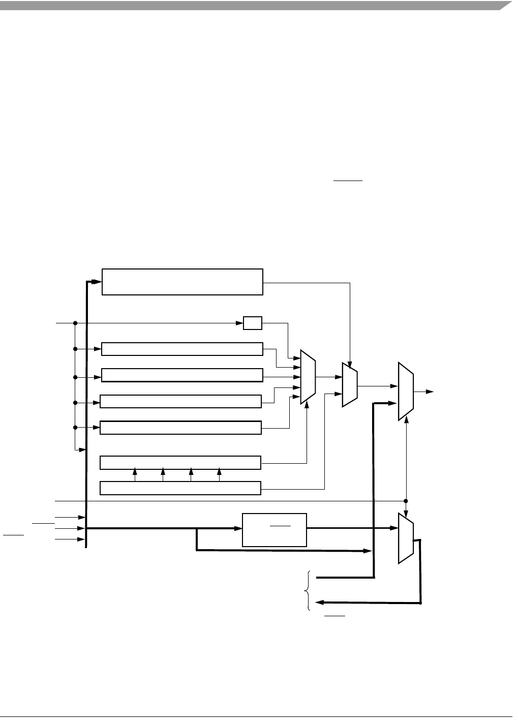
MCF548x Reference Manual, Rev. 3
Freescale Semiconductor 23-1
Chapter 23
IEEE 1149.1 Test Access Port (JTAG)
23.1 Introduction
The Joint Test Action Group, or JTAG, is a dedicated user-accessible test logic, that complies with the
IEEE 1149.1 standard for boundary-scan testability, to help with system diagnostic and manufacturing
testing.
This architecture provides access to all data and chip control pins from the board-edge connector through
the standard four-pin test access port (TAP) and the JTAG reset pin, TRST.
23.1.1 Block Diagram
Figure 23-1 shows the block diagram of the JTAG module.
Figure 23-1. JTAG Block Diagram
4-BIT TAP INSTRUCTION REGISTER
30
1-BIT BYPASS REGISTER
148-BIT BOUNDARY SCAN REGISTER
32-BIT IDCODE REGISTER
TRST/DSCLK
TCK
TMS/BKPT
031
0147
TAP CONTROLLER
TDI/DSI
1
0
TDO/DSO
JTAG Module
to Debug Module
7-BIT JTAG_CFM_CLKDIV REGISTER
0
6
3-BIT TEST_CTRL REGISTER
02
4-BIT TAP INSTRUCTION DECODER
1
0
Disable DSCLK
Force BKPT = 1
DSI = 0
MTMOD0
DSO
DSI
BKPT
DSCLK

MCF548x Reference Manual, Rev. 3
23-2 Freescale Semiconductor
23.1.2 Features
The basic features of the JTAG module are the following:
• Performs boundary-scan operations to test circuit board electrical continuity
• Bypasses instruction to reduce the shift register path to a single cell
• Sets chip output pins to safety states while executing the bypass instruction
• Samples the system pins during operation and transparently shift out the result
• Selects between JTAG TAP controller and Background Debug Module (BDM) using the
MTMOD0 pin
23.1.3 Modes of Operation
The MTMOD0 pin can select between the following modes of operation:
• JTAG mode
• BDM—background debug mode (For more information, refer to Chapter 8, “Debug Support.”)
23.2 External Signal Description
The JTAG module has five input and one output external signals, as described in Table 23-1.
23.2.1 Detailed Signal Description
23.2.1.1 Test Mode 0 (MTMOD0)
The MTMOD0 pin selects between Debug module and JTAG. If MTMOD0 is low, the Debug module is
selected; if it is high, the JTAG is selected. Table 23-2 summarizes the pin function selected depending
upon MTMOD0 logic state.
Table 23-1. Signal Properties
Name Direction Function Reset State Pull up
MTMOD0 Input JTAG/BDM selector input — —
TCK Input JTAG Test clock input — Active
TMS/BKPT Input JTAG Test mode select / BDM Breakpoint — Active
TDI/DSI Input JTAG Test data input / BDM Development serial input — Active
TRST/DSCLK Input JTAG Test reset input / BDM Development serial clock — Active
TDO/DSO Output JTAG Test data output / BDM Development serial output Hi-Z / 0 —

External Signal Description
MCF548x Reference Manual, Rev. 3
Freescale Semiconductor 23-3
When one module is selected, the inputs into the other module are disabled or forced to a known logic level
as shown in Table 23-3, in order to disable the corresponding module.
NOTE
The MTMOD0 does not support dynamic switching between JTAG and
BDM modes.
23.2.1.2 Test Clock Input (TCK)
The TCK pin is a dedicated JTAG clock input to synchronize the test logic. Pulses on TCK shift data and
instructions into the TDI pin on the rising edge and out of the TDO pin on the falling edge. TCK is
independent of the processor clock. The TCK pin has an internal pull-up resistor and holding TCK high or
low for an indefinite period does not cause JTAG test logic to lose state information.
23.2.1.3 Test Mode Select/Breakpoint (TMS/BKPT)
The TMS pin is the test mode select input that sequences the TAP state machine. TMS is sampled on the
rising edge of TCK. The TMS pin has an internal pull-up resistor.
The BKPT pin is used to request an external breakpoint. Assertion of BKPT puts the processor into a halted
state after the current instruction completes.
23.2.1.4 Test Data Input/Development Serial Input (TDI/DSI)
The TDI pin is the LSB-first data and instruction input. TDI is sampled on the rising edge of TCK. The
TDI pin has an internal pull-up resistor.
The DSI pin provides data input for the debug module serial communication port.
Table 23-2. Pin Function Selected
MTMOD0 = 0 MTMOD0 = 1 Pin Name
Module selected BDM JTAG —
Pin Function —
BKPT
DSI
DSO
DSCLK
TCK
TMS
TDI
TDO
TRST
TCK
BKPT
DSI
DSO
DSCLK
Table 23-3. Signal State to the Disable Module
MTMOD0 = 0 MTMOD0 = 1
Disabling JTAG TRST = 0
TMS = 1
—
Disabling BDM — Disable DSCLK
DSI = 0
BKPT = 1

MCF548x Reference Manual, Rev. 3
23-4 Freescale Semiconductor
23.2.1.5 Test Reset/Development Serial Clock (TRST/DSCLK)
The TRST pin is an active low asynchronous reset input with an internal pull-up resistor that forces the
TAP controller to the test-logic-reset state.
The DSCLK pin clocks the serial communication port to the debug module. Maximum frequency is 1/5
the processor clock speed. At the rising edge of DSCLK, the data input on DSI is sampled and DSO
changes state.
23.2.1.6 Test Data Output/Development Serial Output (TDO/DSO)
The TDO pin is the LSB-first data output. Data is clocked out of TDO on the falling edge of TCK. TDO
is tri-stateable and is actively driven in the shift-IR and shift-DR controller states.
The DSO pin provides serial output data in BDM mode.
23.3 Memory Map/Register Definition
23.3.1 Memory Map
The JTAG module registers are not memory mapped and are only accessible through the TDO/DSO pin.
23.3.2 Register Descriptions
All registers are shift-in and parallel load.
23.3.2.1 Instruction Shift Register (IR)
The JTAG module uses a 4-bit shift register with no parity. The IR transfers its value to a parallel hold
register and applies an instruction on the falling edge of TCK when the TAP state machine is in the
update-IR state. To load an instruction into the shift portion of the IR, place the serial data on the TDI pin
before each rising edge of TCK. The MSB of the IR is the bit closest to the TDI pin, and the LSB is the bit
closest to the TDO pin.
23.3.2.2 IDCODE Register
The IDCODE is a read-only register; its value is chip dependent. For more information, see
Section 23.4.3.2, “IDCODE Instruction.”

Memory Map/Register Definition
MCF548x Reference Manual, Rev. 3
Freescale Semiconductor 23-5
23.3.2.3 Bypass Register
The bypass register is a single-bit shift register path from TDI to TDO when the BYPASS instruction is
selected.
23.3.2.4 JTAG_CFM_CLKDIV Register
The JTAG_CFM_CLKDIV register is a 7-bit clock divider for the CFM that is used with the
LOCKOUT_RECOVERY instruction. It controls the period of the clock used for timed events in the CFM
erase algorithm. The JTAG_CFM_CLKDIV register must be loaded before the lockout sequence can
begin.
23.3.2.5 TEST_CTRL Register
The TEST_CTRL register is a 3-bit shift register path from TDI to TDO when the
ENABLE_TEST_CTRL instruction is selected. The TEST_CTRL transfers its value to a parallel hold
register on the rising edge of TCK when the TAP state machine is in the update-DR state.
31 30 29 28 27 26 25 24 23 22 21 20 19 18 17 16
R JTAGID
W
Reset See Table 23-4
Reg
Addr
MBAR + 0x50
15 14 13 12 11 10 9 8 7 6 5 4 3 2 1 0
R JTAGID
W
Reset See Table 23-4
Reg
Addr
MBAR + 0x50
Figure 23-2. JTAG IDCODE Register
Table 23-4. JTAG IDCODE Field Descriptions
Bits Name Description
31–0 JTAGID The JTAG identification number register is a read only register which contains the JTAG ID
number for the MCF548x. Its value is hard coded and cannot be modified.
Values for the MCF548x are the following:
MCF5485 0x0800c01d
MCF5484 0x0800d01d
MCF5483 0x0800e01d
MCF5482 0x0800f01d
MCF5481 0x0801001d
MCF5480 0x0801101d

MCF548x Reference Manual, Rev. 3
23-6 Freescale Semiconductor
23.3.2.6 Boundary Scan Register
The boundary scan register is connected between TDI and TDO when the EXTEST or
SAMPLE/PRELOAD instruction is selected. It captures input pin data, forces fixed values on output pins,
and selects a logic value and direction for bidirectional pins or high impedance for tri-stated pins.
The boundary scan register contains bits for bonded-out and non bonded-out signals excluding JTAG
signals, analog signals, power supplies, compliance enable pins, and clock signals.
23.4 Functional Description
23.4.1 JTAG Module
The JTAG module consists of a TAP controller state machine, which is responsible for generating all
control signals that execute the JTAG instructions and read/write data registers.
23.4.2 TAP Controller
The TAP controller is a state machine that changes state based on the sequence of logical values on the
TMS pin. Figure 23-3 shows the machine’s states. The value shown next to each state is the value of the
TMS signal sampled on the rising edge of the TCK signal.
Asserting the TRST signal asynchronously resets the TAP controller to the test-logic-reset state. As
Figure 23-3 shows, holding TMS at logic 1 while clocking TCK through at least five rising edges also
causes the state machine to enter the test-logic-reset state, whatever the initial state.
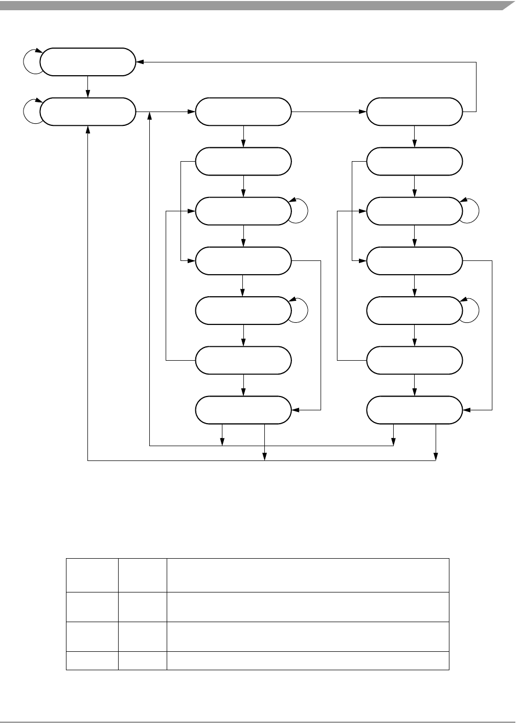
Functional Description
MCF548x Reference Manual, Rev. 3
Freescale Semiconductor 23-7
Figure 23-3. TAP Controller State Machine Flow
23.4.3 JTAG Instructions
Table 23-5 describes public and private instructions.
FTable 23-5. JTAG Instructions
Instructio
nIR[5:0] Instruction Summary
EXTEST 000000 Selects boundary scan register while applying fixed values to output
pins and asserting functional reset
SAMPLE 000001 Selects boundary scan register for shifting, sampling, and preloading
without disturbing functional operation
IDCODE 011101 Selects IDCODE register for shift
RUN-TEST/IDLE
TEST-LOGIC-RESET
1
1
SELECT DR-SCAN
CAPTURE-DR
EXIT1-DR
PAUSE-DR
UPDATE-DR
SELECT IR-SCAN
SHIFT-DR
EXIT2-DR
CAPTURE-IR
SHIFT-IR
EXIT1-IR
PAUSE-IR
EXIT2-IR
UPDATE-IR
0
0
1
1
0
0
0
1
1
10
0
0
1
1
0
0
1
1
0
1
0
1
10
1
1
0
0
1
0

MCF548x Reference Manual, Rev. 3
23-8 Freescale Semiconductor
23.4.3.1 External Test Instruction (EXTEST)
The EXTEST instruction selects the boundary scan register. It forces all output pins and bidirectional pins
configured as outputs to the values preloaded with the SAMPLE/PRELOAD instruction and held in the
boundary scan update registers. EXTEST can also configure the direction of bidirectional pins and
establish high-impedance states on some pins. EXTEST asserts internal reset for the MCU system logic to
force a predictable internal state while performing external boundary scan operations.
23.4.3.2 IDCODE Instruction
The IDCODE instruction selects the 32-bit IDCODE register for connection as a shift path between the
TDI and TDO pin. This instruction allows interrogation of the MCU to determine its version number and
other part identification data. The shift register LSB is forced to logic 1 on the rising edge of TCK
following entry into the capture-DR state.Therefore, the first bit to be shifted out after selecting the
IDCODE register is always a logic 1. The remaining 31 bits are also forced to fixed values on the rising
edge of TCK following entry into the capture-DR state.
IDCODE is the default instruction placed into the instruction register when the TAP resets. Thus, after a
TAP reset, the IDCODE register is selected automatically.
23.4.3.3 SAMPLE/PRELOAD Instruction
The SAMPLE/PRELOAD instruction has two functions:
• SAMPLE —obtain a sample of the system data and control signals present at the MCU input pins
and just before the boundary scan cell at the output pins. This sampling occurs on the rising edge
of TCK in the capture-DR state when the IR contains the $2 opcode. The sampled data is accessible
by shifting it through the boundary scan register to the TDO output by using the shift-DR state.
Both the data capture and the shift operation are transparent to system operation.
NOTE
External synchronization is required to achieve meaningful results because
there is no internal synchronization between TCK and the system clock.
• PRELOAD—initialize the boundary scan register update cells before selecting EXTEST or
CLAMP. This is achieved by ignoring the data shifting out on the TDO pin and shifting in
initialization data. The update-DR state and the falling edge of TCK can then transfer this data to
the update cells. The data is applied to the external output pins by the EXTEST or CLAMP
instruction.
CLAMP 011111 Selects bypass while applying fixed values to output pins and
asserting functional reset
HIGHZ 111101 Selects bypass register while tri-stating all output pins and asserting
functional reset
ENABLE 000010 Selects TEST_CTRL register
BYPASS 111111 Selects bypass register for data operations
Table 23-5. JTAG Instructions (Continued)
Instructio
nIR[5:0] Instruction Summary

Initialization/Application Information
MCF548x Reference Manual, Rev. 3
Freescale Semiconductor 23-9
23.4.3.4 ENABLE_TEST_CTRL Instruction
The ENABLE_TEST_CTRL instruction selects a 3-bit shift register (TEST_CTRL) for connection as a
shift path between the TDI and TDO pin. When the user transitions the TAP controller to the UPDATE_DR
state, the register transfers its value to a parallel hold register. It allows the control chip to test functions
independent of the JTAG TAP controller state.
23.4.3.5 HIGHZ Instruction
The HIGHZ instruction eliminates the need to backdrive the output pins during circuit-board testing.
HIGHZ turns off all output drivers, including the 2-state drivers, and selects the bypass register. HIGHZ
also asserts internal reset for the MCU system logic to force a predictable internal state.
23.4.3.6 CLAMP Instruction
The CLAMP instruction selects the bypass register and asserts internal reset while simultaneously forcing
all output pins and bidirectional pins configured as outputs to the fixed values that are preloaded and held
in the boundary scan update register. CLAMP enhances test efficiency by reducing the overall shift path
to a single bit (the bypass register) while conducting an EXTEST type of instruction through the boundary
scan register.
23.4.3.7 BYPASS Instruction
The BYPASS instruction selects the bypass register, creating a single-bit shift register path from the TDI
pin to the TDO pin. BYPASS enhances test efficiency by reducing the overall shift path when a device
other than the ColdFire processor is the device under test on a board design with multiple chips on the
overall boundary scan chain. The shift register LSB is forced to logic 0 on the rising edge of TCK after
entry into the capture-DR state. Therefore, the first bit shifted out after selecting the bypass register is
always logic 0. This differentiates parts that support an IDCODE register from parts that support only the
bypass register.
23.5 Initialization/Application Information
23.5.1 Restrictions
The test logic is a static logic design, and TCK can be stopped in either a high or low state without loss of
data. However, the system clock is not synchronized to TCK internally. Any mixed operation using both
the test logic and the system functional logic requires external synchronization.
Using the EXTEST instruction requires a circuit-board test environment that avoids device-destructive
configurations in which MCU output drivers are enabled into actively driven networks.
23.5.2 Nonscan Chain Operation
Keeping the TAP controller in the test-logic-reset state ensures that the scan chain test logic is transparent
to the system logic. It is recommended that TMS, TDI, TCK, and TRST be pulled up. TRST could be
connected to ground. However, since there is a pull-up on TRST, some amount of current results. The
internal power-on reset input initializes the TAP controller to the test-logic-reset state on power-up without
asserting TRST.

MCF548x Reference Manual, Rev. 3
23-10 Freescale Semiconductor

MCF548x Reference Manual, Rev. 3
Freescale Semiconductor i
Part IV
Communications Subsystem
Part IV contains chapters that discuss the operation and configuration of the communications I/O
subsystem including the MCF548x multichannel DMA, communications timer, PSC, FEC, DSPI, and
USB2, and I2C.
Contents
Part IV contains the following chapters:
•Chapter 24, “Multichannel DMA,” provides an overview of the multichannel DMA controller
module including the operation of the external DMA request signals.
•Chapter 25, “Comm Timer Module (CTM),” contains a detailed description of the communications
timer module, which functions as a baud clock generator or as a DMA task initiator.
•Chapter 26, “Programmable Serial Controller (PSC),” provides an overview of asynchronous,
synchronous, and IrDA 1.1 compliant receiver/transmitter serial communications of the MCF548x.
•Chapter 27, “DMA Serial Peripheral Interface (DSPI),” describes the use of the DMA serial
peripheral interface (DSPI) implemented on the MCF548x processor, including details of the DSPI
data transfers. The chapter concludes with timing diagrams and the DSPI features that support Tx
and Rx FIFO queue management.
•Chapter 28, “I2C Interface,” describes the MCF548x I2C module, including I2C protocol, clock
synchronization, and the registers in the I2C programing model. It also provides programming
examples.
•Chapter 29, “USB 2.0 Device Controller,” provides an overview of the USB 2.0 device controller
module used in the MCF548x.
•Chapter 30, “Fast Ethernet Controller (FEC),” provides a feature-set overview, a functional block
diagram, and transceiver connection information for both MII (Media Independent Interface) and
7-wire serial interfaces. It also provides describes operation and the programming model.

MCF548x Reference Manual, Rev. 3
ii Freescale Semiconductor
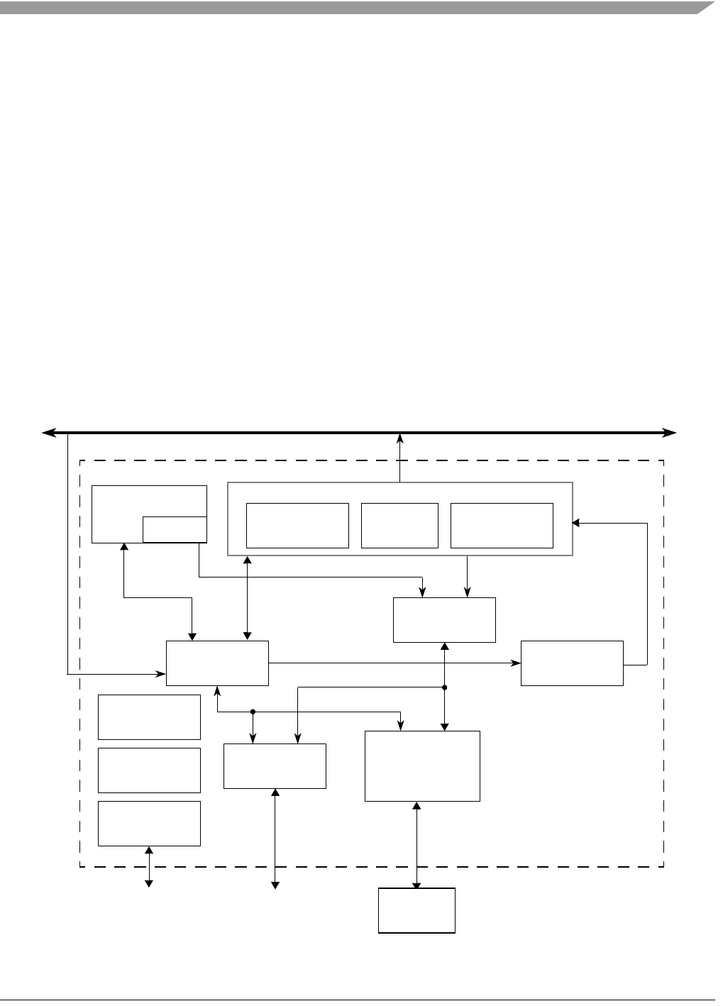
MCF548x Reference Manual, Rev. 3
Freescale Semiconductor 24-1
Chapter 24
Multichannel DMA
24.1 Introduction
The MCF548x’s direct memory access controller (DMA) module provides a flexible and efficient means
to move blocks of data within the system. The multichannel DMA controller reduces the workload on the
microprocessor, allowing it to continue execution of system software. The DMA microcode engine is
tailored to efficiently transfer data across the internal bus architecture to memory and peripheral devices.
Access to the functionality of the multichannel DMA is provided using a software API. The “Multichannel
DMA API User’s Guide” (MCDMAAPIUG) contains a full description of the software API for use with
the DMA. Please refer to that document for software driver information.
24.1.1 Block Diagram
Figure 24-1 shows the internal block structure and data paths within the multichannel DMA module. A
very brief description of each block follows.
Figure 24-1. DMA Block Diagram
Read Arbiter
Priority Task
Decode (PTD)
Read Engine Write Engine
Arbitration
MDE
TaskBAR
Comm Bus
Write Arbiter
LURC
Debug Unit
System Bus
Interface
Line Buffers SRAM Interface
Data In
ADS
32 Kbyte
SRAM
DMA
Controller
XL Bus
Data Out
IP Bus System

MCF548x Reference Manual, Rev. 3
24-2 Freescale Semiconductor
24.1.2 Overview
The DMA controller processes microcode tasks that are stored in memory. A task is a sequence of
instructions, referred to as descriptors, that specifies a series of data movements or manipulations. The
DMA controller steps through the descriptors and executes the specified function in a similar fashion to a
CPU executing a program.
24.1.2.1 Master DMA Engine (MDE)
The MDE is the main interpreter for the multichannel DMA. It parses descriptors and sets up the other
blocks to perform the actual data movement and manipulation. It also manages context switches. For more
MDE information see Section 24.5, “Programming Model.”
24.1.2.2 Address and Data Sequencer (ADS)
The ADS is the engine that pumps data through the multichannel DMA. Based on configuration bits set
by the MDE (derived from the application program), the ADS will fetch operands, route them through
execution units, store results as appropriate, and evaluate termination conditions.
24.1.2.3 Priority-Task Decoder (PTD)
The PTD manages prioritization of initiators and maintains the mapping from initiator to task number. The
user has complete control of initiator priority. The PTD also maintains error status and control.
24.1.2.4 Logic Unit with Redundancy Check (LURC)
The LURC can perform several arithmetic and logical operations including addition, subtraction, logical
shifts, binary operations, and checksum calculations. The LURC can perform as many as five boolean
operations on up to four operands and provides an efficient mechanism for performing endian conversions.
The checksum unit can compute the following CRC polynomials: CRC-32, CRC-16, CRC-CCITT, and
the internet checksum.
24.1.2.5 Debug Unit
The Debug unit provides simple breakpoint functionality to halt tasks when they reach certain conditions.
24.1.3 Features
The DMA module has the following features:
• A programmatic, deterministic capability for managing bus resources while servicing many data
streams with individual latency and processing requirements.
• Single cycle access of peripheral and memory data.
• Support for up to 16 simultaneously enabled tasks (channels)
• Support for up to 32 separate DMA initiators at a time
• Simultaneous 32-bit reads and writes for many sources and targets
• Checksum generation
• Endian conversion
• Chaining/scatter-gather capability
• Support for packet-based I/O protocols

External Signals
MCF548x Reference Manual, Rev. 3
Freescale Semiconductor 24-3
24.2 External Signals
24.2.1 DREQ[1:0]
These active-low inputs provide external requests from peripherals needing DMA service. When asserted,
the device is requesting service. Depending on the operating mode, either the level of the signal is sampled
at the rising edge of the system clock or an edge detect is used to recognize a high to low change. These
inputs have no effect when the task enable control bit is cleared.
24.2.2 DACK[1:0]
These active-low outputs indicate when the DMA request is being acknowledged. These outputs can be
programmed to assert from one to four system clocks, depending on the operating mode. The DACK
signals are programmed to recognize the address on one of the DMA address buses and assert if a match
is made. The size of the address space can be increased by setting the EREQMASKn address mask bits.
See Section 24.3.4.3, “External Request Address Mask Register (EREQMASK),” for more information.
24.3 Memory Map/Register Definitions
Memory organization is described in the register array pointed to by the memory base address register
(MBAR). Information necessary to enable the DMA is described in this register array at the predetermined
offset of MBAR + 0x8000.
The TaskBAR identifies a location for the table of pointers to multichannel DMA tasks. Each task has an
entry that contains information about the microcode’s location in memory as well as a pointer to the
variable table to be used in the task.
In the MCF548x, DMA memory is controlled both by the programmer and by the DMA engine itself.
24.3.1 DMA Task Memory
The DMA uses memory provided by the user to store task code and structures. Figure 24-2 shows some
of the structures in DMA memory. This memory region may exist in any addressable storage, such as
system SRAM or external memory.
24.3.1.1 Task Table
The task table is a memory region containing pointers to each MDE task. A task table base address register
(taskBAR) sets the location of the task table itself. Each entry in the task table contains pointers to the
task’s first descriptor, last descriptor, variable table, and other task-specific information. The task table
must be aligned to a 512-byte boundary.
24.3.1.2 Task Descriptor Table
Each task descriptor table is a memory region containing the descriptors that comprise the task. Each task
descriptor table is composed of Data Routing Descriptors (DRD) and Loop Control Descriptors (LCD).
The pointers in the task table define the beginning and end of each task descriptor table; see Figure 24-2.
Task descriptor tables must be aligned to a longword (32 bit) boundary.

MCF548x Reference Manual, Rev. 3
24-4 Freescale Semiconductor
24.3.1.3 Variable Table
Each task has a private 48-longword variable table. Typically, each variable table must be aligned to a
256-byte boundary, though some may be aligned to a 128-byte boundary if the task uses 32 or less
variables.
24.3.1.4 Function Descriptor Table
Function descriptor tables are 256-byte tables that hold the operation codes to be passed to the DMA
execution units when data manipulation is performed. Each function descriptor table must be aligned to a
256-byte boundary. Each function descriptor table is divided into four 64-byte areas, one for each potential
execution unit. This implementation of the multichannel DMA only contains one execution unit, the
LURC, and it uses the last (fourth) 64-byte area.
24.3.1.5 Context Save Space
Each task has a context save space that the DMA uses to save internal context in when a task is swapped
out of operation. When a task is swapped back into operation, the internal context can be retrieved from
the context save space.
24.3.2 Memory Structure
Each of these memory regions may exist in any addressable storage, such as internal system SRAM or
external memory (internal system SRAM is recommended).
Figure 24-2 illustrates the memory regions that are programmer maintained.
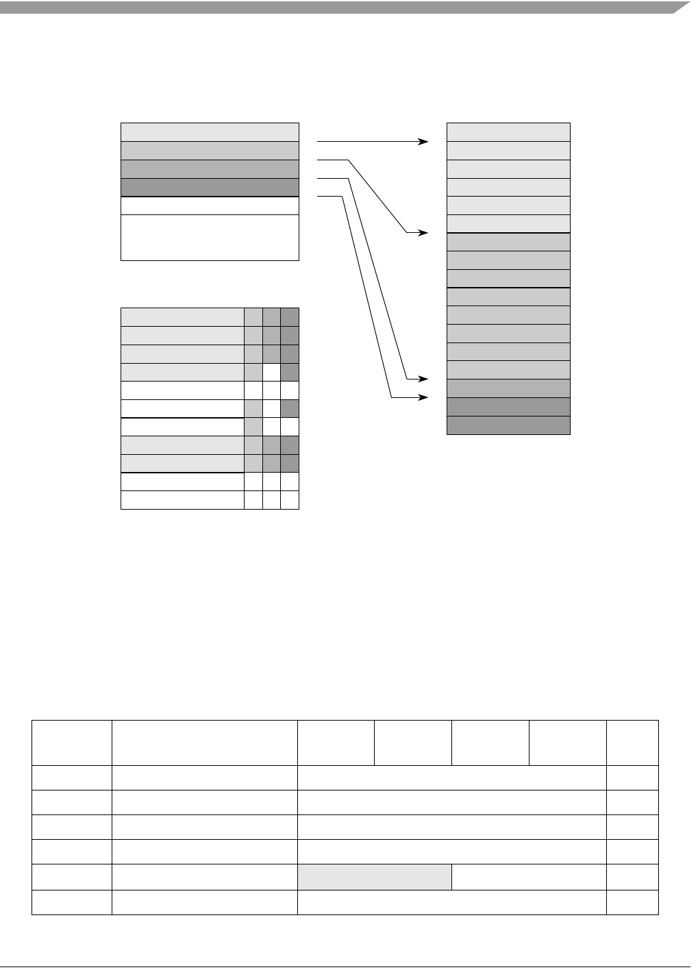
Memory Map/Register Definitions
MCF548x Reference Manual, Rev. 3
Freescale Semiconductor 24-5
Figure 24-2. DMA Programmer-Maintained Memory Model
24.3.3 DMA Registers
24.3.3.1 DMA Register Map
Table 24-1 shows the memory map of the DMA module.
Table 24-1. DMA Memory Map
Address
(MBAR +) Name Byte0 Byte1 Byte2 Byte3 Access
0x8000 Task Base Address Register TaskBAR R/W
0x8004 Current Pointer CP R
0x8008 End Pointer EP R
0x800C Variable Pointer VP R
0x8010 PTD Control Register PTD R/W
0x8014 DMA Interrupt Pending Register DIPR R/W
Start, End,
Variable Table Pointer,
Control
Task 0 Pointers, Control LCD00
DRD0
1
LCD1
2
LCD23
DRD24
DRD15
LCD3
6
LCD47
DRD4
8
DRD3
9
LCD5
10
LCD611
DRD612
DRD513
LCD7n–1
DRD7
n
Task 1 Pointers, Control
Task 2 Pointers, Control
Task 3 Pointers, Control
Initial Value0 0
Initial Value1 1
Initial Value2 2
Initial Value3 3
22
23
Increment0 24
Increment1 25
31
Task 0
Task 1
Task 2
Task 3
Task 15
•
•
•
•
•
•
•
•
•
Variable Table
Pointed to by Task Table
Task Table
Pointed to by TaskBAR Task Descriptor Table
Programmer-Maintained,
Located in Memory
Shadings indicate different tasks.
Four tasks shown.

MCF548x Reference Manual, Rev. 3
24-6 Freescale Semiconductor
24.3.3.2 Task Base Address Register (TaskBAR)
Note that there is a 512-byte alignment restriction on the TaskBAR.
0x8018 DMA Interrupt Mask Register DIMR R/W
0x801C Task Control Register TCR0 TCR1 R/W
0x8020 Task Control Register TCR2 TCR3 R/W
0x8024 Task Control Register TCR4 TCR5 R/W
0x8028 Task Control Register TCR6 TCR7 R/W
0x802C Task Control Register TCR8 TCR9 R/W
0x8030 Task Control Register TCR10 TCR11 R/W
0x8034 Task Control Register TCR12 TCR13 R/W
0x8038 Task Control Register TCR14 TCR15 R/W
0x803C Priority Register PRIOR0 PRIOR1 PRIOR2 PRIOR3 R/W
0x8040 Priority Register PRIOR4 PRIOR5 PRIOR6 PRIOR7 R/W
0x8044 Priority Register PRIOR8 PRIOR9 PRIOR10 PRIOR11 R/W
0x8048 Priority Register PRIOR12 PRIOR13 PRIOR14 PRIOR15 R/W
0x804C Priority Register PRIOR16 PRIOR17 PRIOR18 PRIOR19 R/W
0x8050 Priority Register PRIOR20 PRIOR21 PRIOR22 PRIOR23 R/W
0x8054 Priority Register PRIOR24 PRIOR25 PRIOR26 PRIOR27 R/W
0x8058 Priority Register PRIOR28 PRIOR29 PRIOR30 PRIOR31 R/W
0x805C InitiatorMuxControl IMCR —
0x8060 Task Size Register 0 TSKSZ0 R/W
0x8064 Task Size Register 1 TSKSZ1 R/W
0x8068 -
0x806f
Reserved
0x8070 Debug Comparator 1 DBGCOMP1 R/W
0x8074 Debug Comparator 2 DBGCOMP2 R/W
0x8078 Debug Control DBGCTL R/W
0x807C Debug Status DBGSTAT R/W
0x8080 PTD Debug Registers PTDDBG R1
1Writes must be to this address first to select the next register to read.
Table 24-1. DMA Memory Map (Continued)
Address
(MBAR +) Name Byte0 Byte1 Byte2 Byte3 Access

Memory Map/Register Definitions
MCF548x Reference Manual, Rev. 3
Freescale Semiconductor 24-7
24.3.3.3 Current Pointer (CP)
31 30 29 28 27 26 25 24 23 22 21 20 19 18 17 16
R Task Base Address
W
Reset Uninitialized
1514131211109876543210
RTask Base Address
W
Reset Uninitialized
Reg
Addr
MBAR + 0x8000
Figure 24-3. Task Base Address Register (TaskBAR)
Table 24-2. TaskBAR Field Descriptions
Bits Name Description
31–0 Task Base Address Task base address. Pointer to the base address of the DMA task table.
31 30 29 28 27 26 25 24 23 22 21 20 19 18 17 16
R Descriptor Pointer
W
Reset Uninitialized
1514131211109876543210
RDescriptor Pointer
W
Reset Uninitialized
Reg
Addr
MBAR + 0x8004
Figure 24-4. Current Pointer Register (CP)
Table 24-3. CP Field Descriptions
Bits Name Description
31–0 Descriptor
Pointer
Descriptor pointer. Pointer to the address of the DMA descriptor that is currently executing.

MCF548x Reference Manual, Rev. 3
24-8 Freescale Semiconductor
24.3.3.4 End Pointer (EP)
24.3.3.5 Variable Pointer (VP)
31 30 29 28 27 26 25 24 23 22 21 20 19 18 17 16
R Descriptor Pointer
W
Reset Uninitialized
1514131211109876543210
RDescriptor Pointer
W
Reset Uninitialized
Reg
Addr
MBAR + 0x8008
Figure 24-5. End Pointer Register (EP)
Table 24-4. EP Field Descriptions
Bits Name Description
31–0 Descriptor
Pointer
Descriptor pointer. Pointer to the address of the last DMA descriptor for the currently
executing task.
31 30 29 28 27 26 25 24 23 22 21 20 19 18 17 16
RVariable Pointer
W
Reset Uninitialized
1514131211109876543210
RVariable Pointer
W
Reset Uninitialized
Reg
Addr
MBAR + 0x800C
Figure 24-6. Variable Pointer Register (VP)
Table 24-5. VP Field Descriptions
Bits Name Description
31–0 Variable
Pointer
Variable pointer. Pointer to the starting address of the variable table for the currently
executing task.

Memory Map/Register Definitions
MCF548x Reference Manual, Rev. 3
Freescale Semiconductor 24-9
24.3.3.6 PTD Control (PTD)
The priority task decode control register is used to configure different operating modes of this DMA
module. The PTD is also used to enable/disable new functionality designed into the module after the first
release of the design.
31 30 29 28 27 26 25 24 23 22 21 20 19 18 17 16
R0000000000000000
W
Reset0000111100001111
1514131211109875543210
RPCTL
15
PCTL
14
PCTL
13
00000000000PCTL
1
0
W
Reset0000000000000000
Reg
Addr
MBAR + 0x8010
Figure 24-7. PTD Control Register (PTD)
Table 24-6. PTD Field Descriptions
Bits Name Description
31–16 — Reserved.
15 PCTL15 Task priority control. This bit selects the prioritization scheme used by the DMA when deciding
which tasks to run. This is a global bit and affects all DMA channels. See Section 24.4.5,
“Prioritization,” and Section 24.3.3.10, “Priority Registers (PRIORn),” for further reference.
1 Task priority
0 Request priority
14 PCTL14 Bus error control
0 Enable interrupt for bus error
1 Disable interrupt for bus error
13 PCTL13 Task arbitration control
0 Do not force arbitration
1 Force arbitration for higher task number on same request level
12–2 — Reserved
1 PCTL1 Registered request control
0 Take request straight from FIFO controller
1 Enable registered Requester from prefetch buffer
0 PCTL0 CommBus Prefetch
1 disable prefetch
0 enable prefetch

MCF548x Reference Manual, Rev. 3
24-10 Freescale Semiconductor
24.3.3.7 DMA Interrupt Pending (DIPR)
24.3.3.8 DMA Interrupt Mask Register (DIMR)
31 30 29 28 27 26 25 24 23 22 21 20 19 18 17 16
R0000000000000000
W
Reset0000000000000000
1514131211109876543210
R TASK
15
TASK
14
TASK
13
TASK
12
TASK
11
TASK
10
TASK
9
TASK
8
TASK
7
TASK
6
TASK
5
TASK
4
TASK
3
TASK
2
TASK
1
TASK
0
W
Reset0000000000000000
Reg
Addr
MBAR +0x8014
Figure 24-8. DMA Interrupt Pending Register (DIPR)
Table 24-7. DIPR Field Descriptions
Bits Name Description
31–16 — Reserved
15–0 TASKnInterrupt Pending. Each bit corresponds to an interrupt source defined by the task number. The
corresponding bit in this register reflects the state of the interrupt signal even if the corresponding
mask bit is set. A bit is cleared by writing a 1 to that bit location; writing a zero has no effect. At
system reset, all bits are initialized to logic zeros.
0 The corresponding interrupt source not pending
1 The corresponding interrupt source pending
31 30 29 28 27 26 25 24 23 22 21 20 19 18 17 16
R0000000000000000
W
Reset1111111111111111
1514131211109876543210
R TASK
15
TASK
14
TASK
13
TASK
12
TASK
11
TASK
10
TASK
9
TASK
8
TASK
7
TASK
6
TASK
5
TASK
4
TASK
3
TASK
2
TASK
1
TASK
0
W
Reset1111111111111111
Reg
Addr
MBAR + 0x8018
Figure 24-9. DMA Interrupt Mask Register (DIMR)

Memory Map/Register Definitions
MCF548x Reference Manual, Rev. 3
Freescale Semiconductor 24-11
24.3.3.9 Task Control Registers (TCRn)
Each of the sixteen tasks has an associated task control register. Only one register is shown. At system
reset, all bits are initialized to logic zeros.
Table 24-8. DIMR Field Descriptions
Bits Name Description
31–16 — Reserved
15–0 TASKnInterrupt mask. Each bit corresponds to an interrupt source defined by the task number. An
interrupt is masked by setting the corresponding bit in the IMR. At system reset, all bits are
initialized to logic ones.
0 The corresponding interrupt source is not masked
1 The corresponding interrupt source is masked
15141312111098 7 6 5 43210
REN V ALW
INIT
INITNUM ASTRT HIPRI
TSKEN
HLDINIT
NUM
0 ASTSKNUM
W
Reset00000000 0 0 0 00000
Reg
Addr
MBAR + 0x801C (TCR0), 0x801E (TCR1), 0x8020 (TCR2), 0x8022 (TCR3), 0x8024 (TCR4), 0x8026 (TCR5), 0x8028 (TCR6),
0x802A (TCR7), 0x802C (TCR8), 0x280E (TCR9), 0x3800 (TCR10), 0x8032 (TCR11), 0x8034 (TCR12), 0x8036 (TCR13),
0x8038 (TCR14), 0x803A (TCR15)
Figure 24-10. Task Control Register (TCRn)
Table 24-9. TCRn Field Descriptions
Bits Name Description
15 EN Task enable. Setting this bit will start the task.This bit can be set or cleared by the programmer
at any time when a task is enabled or disabled. This bit is also set by the PTD logic if the
auto-restart bit is set and the task completes.
0 Disabled
1 Enabled
14 V Initiator number is valid. This bit is set by the PTD logic when the MDE obtains the initiator value
from the first DRD that is parsed. This bit is cleared by the PTD logic when the task completes.
At system reset, this bit is cleared.
0 Initiator is not valid
1 Initiator is valid
13 ALWINIT Decode of the always initiator. This bit is a status only bit and is set and cleared by writing the
initiator number into the Task Control Register. When the always initiator number (0) is written
to the Task Control Register by the user or the MDE the ALWINIT bit is set. When a different
initiator number is written to the Task Control Register , then the ALWINIT bit is cleared.
0 The always initiator is not being used
1 The always initiator is being used
12–8 INITNUM Initiator number from task descriptor. These bits are registered when the MDE has parsed the
first DRD to obtain the initiator number. These bits are cleared by system reset. These bits can
be written by the programmer when the HLDINITNUM bit is set or being set and the task is not
enabled.

MCF548x Reference Manual, Rev. 3
24-12 Freescale Semiconductor
24.3.3.10 Priority Registers (PRIORn)
When the PTD Control register bit 15 is set to a logic one, the first 16 Priority Registers are used to set the
associated priority level of the corresponding task. The last 16 Priority registers are unused in this case.
When PTD[PCTL15] is set to zero, the 32 Priority registers are used to set the associtated priority level of
the corresponding initiator. Only one register is shown. At system reset, all bits are initialized to a logic
zero.
7 ASTRT Auto start. This bit can be set or cleared by the programmer at any time. This bit is also cleared
if the MDE encounters an error in the task. At system reset, this bit is cleared.Setting this bit
instructs the MDE to start the task indicated by the ASTSKNUM field once the current task
completes.
0 Task will not start at end of taskl
1 Task will start at end of task
6 HIPRITSKEN High-priority task enable. This bit can be set or cleared by the programmer at any time. This bit
enables the MDE to give priority to the enable task function over a running task. At system
reset, this bit is cleared.
0 Normal task enable control
1 High priority task enable control
5 HLDINITNUM Hold initiator number. This bit allows the initiator number to be set by the programmer and held
for the complete task. The MDE module can not overwrite the programmed initiator except for
the use of the always initiator which is contained in a separate control bit.
0 Allow the MDE module to update initiator number for task
1 Keep current initiator number
4 — Reserved.
3–0 ASTSKNUM Auto-start task number. These four bits contain the task number that will be auto-started when
the ASTRT control bit is set. At system reset, these bits are cleared.
76543210
RHLD0000 PRI
W
Reset00000000
Reg
Addr
MBAR + 0x803C (PR0), 0x803D (PR1), 0x803E (PR2), 0x803F (PR3), 0x8040 (PR4), 0x8041 (PR5),
0x8042 (PR6), 0x8043 (PR7), 0x8044 (PR8), 0x8045 (PR9), 0x8046 (PR10), 0x8047 (PR11), 0x8048 (PR12),
0x8049(PR13), 0x804A (PR14), 0x804B (PR15), 0x804C(PR16), 0x804D(PR17), 0x804E (PR18), 0x804F (PR19),
0x8050 (PR20), 0x8051 (PR21), 0x8052 (PR22), 0x8053 (PR23), 0x8054 (PR24), 0x8055 (PR25), 0x8056 (PR26),
0x8057 (PR27), 0x8058 (PR28), 0x8059 (PR29), 0x805A (PR30), 0x805B (PR31)
Figure 24-11. Priority Register
Table 24-9. TCRn Field Descriptions (Continued)
Bits Name Description

Memory Map/Register Definitions
MCF548x Reference Manual, Rev. 3
Freescale Semiconductor 24-13
24.3.3.11 Initiator Mux Control Register (IMCR)
The DMA supports up to 32 simultaneous DMA request sources, or initiators. For systems where the
number of initiators can exceed 32, it is possible to mux them such that there is user control of which 32
are active at any time. Because there are more than 32 possible DMA initiators on the MCF548x, some of
the initiators are multiplexed to provide software control of which 32 are active at any time. Figure 24-13
shows how the assignments are made from a particular request device to its request number. Sixteen
initiators are always valid, and up to 64 initiators have muxing options for the other 16 request slots. A
single initiator can have multiple muxing options, but only one path should be enabled at a time.
Table 24-10. PRIOR Field Descriptions
Bits Name Description
7 HLD Keep current priority of initiator. This bit can be set or cleared by the programmer at any time. This
bit allows the current initiator to hold priority until the initiator has negated or the task has finished.
When this bit is cleared, an initiator with a higher priority will block the current initiator and force
arbitration. At system reset, this bit is cleared.
0 Allow higher priority initiator to block current initiator
1 Hold current initiator priority level
Note: Setting this bit in task priority allows a low priority task which is currently executing to
complete before allowing a higher priority task to be executed and therefore may not be desirable.
6–3 — Reserved.
2–0 PRI Priority level. These bits are set by the programmer at any time. The PRI field controls the service
priority of tasks by assigning each task a priority level. The highest priority level is 7 and the lowest
priority level is 0. If more than one task/ initiator contains the same priority then the higher numbered
task will take precedence.
313029282726252423222120191817161514131211109876543210
R
W
Initiator Mux Control
Reset00000000000000000000000000000000
Reg
Addr
MBAR + 0x805C
Figure 24-12. Initiator Mux Control Register (IMCR)
Figure 24-13. Initiator Assignments
Request
Number (of
Source)
Initiator Mux
Control
Register Bit
Encoding
00 01 10 11
0 none ALWAYS (This initiator is always asserted)
1 none DSPI RxFIFO
2 none DSPI TxFIFO
3 none DREQ0
4 none PSC0 Rx
5 none PSC0 Tx

MCF548x Reference Manual, Rev. 3
24-14 Freescale Semiconductor
24.3.3.12 Task Size Registers (TSKSZ[0:1])
Each of the 16 tasks can be programmed to use specific source and destination sizes contained in a task
size register instead of a specific type encoded in a DRD. The ADS module uses the task size register
information to determine the source and destination transfer size of the operands. When the size contained
in the DRD is set to 2’b11 then specific source and destination size fields from the task size register are
selected.
6 none USB device Tx/Rx endpoint 0
7 none USB device Tx/Rx endpoint 1
8 none USB device Tx/Rx endpoint 2
9 none USB device Tx/Rx endpoint 3
10 none PCI Tx
11 none PCI Rx
12 none PSC1 Rx
13 none PSC1 Tx
14 none I2C Rx
15 none I2C Tx
16 1:0 FEC0 Rx Reserved
17 3:2 FEC0 Tx Reserved
18 5:4 Reserved Reserved FEC0 Rx
19 7:6 Reserved Reserved FEC0 Tx Reserved
20 9:8 Reserved FEC1 Rx Reserved Reserved
21 11:10 DREQ1 FEC1 Tx Reserved Reserved
22 13:12 Reserved FEC0 Rx Reserved Reserved
23 15:14 Reserved FEC0 Tx Reserved Reserved
24 17:16 Reserved CommTimer0 FEC1 Rx Reserved
25 19:18 Reserved CommTimer1 FEC1 Tx Reserved
26 21:20 USB Endpoint 4 Reserved CommTimer2 Reserved
27 23:22 USB Endpoint 5 Reserved CommTimer3 Reserved
28 25:24 USB Endpoint 6 CommTimer4 DREQ1 PSC2 Rx
29 27:26 Reserved DREQ1 CommTimer5 PSC2Tx
30 29:28 FEC1 Rx CommTimer6 Reserved PSC3 Rx
31 31:30 FEC1 Tx Reserved CommTimer7 PSC3 Tx
Figure 24-13. Initiator Assignments (Continued)
Request
Number (of
Source)
Initiator Mux
Control
Register Bit
Encoding
00 01 10 11

Memory Map/Register Definitions
MCF548x Reference Manual, Rev. 3
Freescale Semiconductor 24-15
31 30 29 28 27 26 25 24 23 22 21 20 19 18 17 16
TASK0 TASK1 TASK2 TASK3
R SRCSZ DSTSZ SRCSZ DSTSZ SRCSZ DSTSZ SRCSZ DSTSZ
W
Reset0000000000000000
1514131211109876543210
TASK4 TASK5 TASK6 TASK7
R SRCSZ DSTSZ SRCSZ DSTSZ SRCSZ DSTSZ SRCSZ DSTSZ
W
Reset0000000000000000
Reg
Addr
MBAR + 0x8060 (TSKSZ0)
Figure 24-14. Task Size Register 0 (TSKSZ0)
31 30 29 28 27 26 25 24 23 22 21 20 19 18 17 16
TASK8 TASK9 TASK10 TASK11
R SRCSZ DSTSZ SRCSZ DSTSZ SRCSZ DSTSZ SRCSZ DSTSZ
W
Reset0000000000000000
1514131211109876543210
TASK12 TASK13 TASK14 TASK15
R SRCSZ DSTSZ SRCSZ DSTSZ SRCSZ DSTSZ SRCSZ DSTSZ
W
Reset0000000000000000
Reg
Addr
MBAR +0x8064 (TSKSZ1)
Figure 24-15. Task Size Register 1 (TSKSZ1)
Table 24-11. TSKSZ Field Descriptions
Bits Name Descriptions
31:30, 27:26,
23:22, 19:18,
15:14, 11:10,
7:6, 3:2
SRCSZ Source size
00 Longword
01 Byte
1x Word
29:28, 25:24,
21:20, 17:16,
13:12, 9:8, 5:4,
1:0
DSTSZ Destination size
00 Longword
01 Byte
1x Word

MCF548x Reference Manual, Rev. 3
24-16 Freescale Semiconductor
24.3.3.13 Debug Comparator Registers (DBGCOMPn)
24.3.3.14 Debug Control (DBGCTL)
31 30 29 28 27 26 25 24 23 22 21 20 19 18 17 16
R Comparator Value
W
Reset0000000000000000
1514131211109876543210
RComparator Value
W
Reset0000000000000000
Reg
Addr
MBAR + 0x8070
Figure 24-16. Debug Comparator Register (DBGCMPn)
Table 24-12. Debug Comparator Field Descriptions
Bits Name Description
31–0 Comparator
Value
Comparator value for comparator 1 or comparator 2.
31 30 29 28 27 26 25 24 23 22 21 20 19 18 17 16
R Block Tasks[15:0]
W
Reset0000000000000000
1514131211109876543210
RAA BComparator 1 Type Comparator 2 Type AND/
OR
0 0 0 0 E I 0
W
Reset0000000000000000
Reg
Addr
MBAR + 0x8078
Figure 24-17. Debug Control Register (DBGCTL)

Memory Map/Register Definitions
MCF548x Reference Manual, Rev. 3
Freescale Semiconductor 24-17
Table 24-14 below shows the encodings for the comparator 1 type bits. These bits are set to 000 at reset
signifying an uninitialized state.
Table 24-13. Debug Control Field Descriptions
Bits Name Description
31–16 Block Tasks Specify for each of tasks 15-0, whether to block that task with detection of a breakpoint
0 Do not block task
1 Block the task
15 AA AutoArm—The bit specifies whether or not the triggered bit dbgStatusReg[16] will be automatically
reset to 0 following the saving of context for a breakpoint. This bit is set to 0 at reset.
0 Triggered bit will not be automatically reset
1 Triggered bit will be automatically reset
14 B Breakpoint—This bit specifies whether or not to take a breakpoint. This bit is set to 0 at reset.
0 Disable breakpoints
1 Enable breakpoints
13-11 Comparator
Type 1
Comparator 1 type—These bits specify the type of data that has been loaded into comparator 1;
refer to Table 24-14 for the bit encodings.
10-8 Comparator
Type 2
Comparator 2 type—These bits specify the type of data that has been loaded into comparator 2;
refer to Table 24-15 for the bit encodings
7 AND/OR AND/OR—This specifies what type of operation is to be used with the comparators. This bit is set
to 0 at reset.
0 Indicates a OR’ing of the comparators
1 Indicates a AND’ing of the comparators
6-3 Reserved.
2 E Enable external breakpoint.
0 Do not enable external breakpoint to cause a halt condition
1 Allow external breakpoint to cause a halt condition
1 I Enable internal breakpoint
0 Do not enable internal breakpoint to cause a halt condition
1 Allow internall breakpoint to cause a halt condition
0 — Reserved.
Table 24-14. Comparator 1 Type Bit Encoding
Encodings Comparator 1 Type
000 uninitialized
001 write address
010 read address
011 current pointer
100 task #
101 reserved
110 reserved
111 reserved

MCF548x Reference Manual, Rev. 3
24-18 Freescale Semiconductor
Table 24-15 below shows the encodings for the bits. These bits are set to 101 at reset signifying an
uninitialized state.
24.3.3.15 Debug Status (DBGSTAT)
Table 24-15. Comparator 2 Type Bit Encodings
Encodings Comparator 2 Type
000 uninitialized
001 write address
010 read address
011 current pointer
100 task #
101 counter value
110 reserved
111 reserved
31 30 29 28 27 26 25 24 23 22 21 20 19 18 17 16
R0 0 0 0 000000000IET
Ww1c w1c
Reset0000000000000000
1514131211109876543210
R Task Blocked[15:0]
Ww1c
Reset0000000000000000
Reg
Addr
MBAR + 0x807C
Figure 24-18. Debug Status Register (DBGSTAT)
Table 24-16. Debug Status Field Descriptions
Bits Name Description
31-19 — Reserved.
18 I Interrupt. This bit indicates whether or not a interrupt has been taken. This bit is set to 0 at reset. It
can be written by the user or the PTD.
0 No Interrupt
1 Interrupt taken
17 E External Breakpoint. This bit indicates detection of an external breakpoint. Status bit is sticky and
requires a 1 to be written to it to clear it. The writing of a 0 to this bit has no effect. This bit is set to
0 at reset.
0 No external breakpoint detected
1 E xternal breakpoint detected

Memory Map/Register Definitions
MCF548x Reference Manual, Rev. 3
Freescale Semiconductor 24-19
24.3.3.16 PTD Debug Registers
The PTD Debug register allows access to internal read-only PTD status registers. A different internal status
register can be viewed by writing to the register. That register will stay selected until a different value is
written to this location (MBAR+0x8080), and the next time this address is read, the corresponding register
will be driven.
16 T Triggered.This bit indicates that a DMA breakpoint has occurred with the current settings. Status bit
is sticky and requires a 1 to be written to it to clear it. The writing of a 0 to this bit has no effect. This
bit is set to 0 at reset.
0 Armed or normal operation
1 Triggered or debug mode
15–0 Task
Blocked
Task Blocked. Each bit corresponds to one of the 16 task numbers. The value of the register bit
reflects the debug state of the task number. A bit is cleared by writing a 1 to that bit location; writing
a 0 has no effect. At system reset, all bits are initialized to logic zero.
0 Unblocked or normal operation
1 Blocked, task has been blocked due to a breakpoint
31 30 29 28 27 26 25 24 23 22 21 20 19 18 17 16
R PTDDBG[31:16]
W
Reset0000000000000000
1514131211109876543210
R PTDDBG[15:0]
W
Reset0000000000000000
Reg
Addr
MBAR + 0x8080
Figure 24-19. PTD Debug Register (PTDDBG)
Table 24-17. PTD Debug Register Descriptions
Value
Written Reg Name Description
0 Request PTDDBG[31:0] reflects the current status of the 31 initiators described in the Initiator Mux
Control Register (IMCR).
1 regInitiator PTDDBG[15:0] reflects whether the corresponding task is valid and the current initiator for
that task is asserted.
2 taskValid PTDDBG[15:0] reflects the state of the V bit (initiator is valid) in each of the Task Control
Registers (TCRs).
3 hold PTDDBG[15:0] reflects the state of the HLD bit in the priority registers for the
corresponding task.
Table 24-16. Debug Status Field Descriptions (Continued)
Bits Name Description

MCF548x Reference Manual, Rev. 3
24-20 Freescale Semiconductor
24.3.4 External Request Module Registers
The following section shows the registers contained within the multichannel DMA external request
module. Details are given regarding register mapping, programming notes, bit definitions, and operating
modes.
24.3.4.1 External Request Module Register Map
The following table shows the register mapping of the external request module.
Because each channel contains the same set of registers, only one set of registers will be defined.
24.3.4.2 External Request Base Address Register (EREQBAR)
After DREQ is asserted, this register contains an address value used for the compare that determines a hit
for the external acknowledge signal, DACK. This address value can be valid for comm bus cycles, system
SRAM, external memory, or comm bus peripherals. This register can be read or written at any time. The
reset state of this register is set to all zeros.
4 taskEnable PTDDBG[15:0] reflects the state of the EN (task enable) bit in each of the Task Control
Registers (TCRs).
5 taskRun PTDDBG[15:0] reflects whether the corresponding task is enabled, valid and not blocked
by the debug module.
6 dbgTaskBlock PTDDBG[15:0] reflects the state of the Task Blocked field of the Debug Status register
(DBGSTAT).
7 alwaysInit PTDDBG[15:0] reflects the state of the ALWINIT bit in each of the Task Control Registers
(TCRs).
8 taskStart PTDDBG[15:0] reflects the state of the Auto-start (ASTRT) bit in each task’s control
register (TCR).
Table 24-18. External Request Module Register Mapping
Address
(MBAR +) Name Byte0 Byte1 Byte2 Byte3 Access
0x0D00
Initiator 1
Base Address Register 0 EREQBAR0 R/W
0x0D04 Base Address Mask Register 0 EREQMASK0 R/W
0x0D08 Control Reg 0 EREQCTRL0 R/W
0x0D0C Reserved
0x0D10
Initiator 2
Base Address Register 1 EREQBAR1 R/W
0x0D14 Base Address Mask Register 1 EREQMASK1 R/W
0x0D18 Control Reg 1 EREQCTRL1 R/W
0x0D1C Reserved
Table 24-17. PTD Debug Register Descriptions (Continued)
Value
Written Reg Name Description

Memory Map/Register Definitions
MCF548x Reference Manual, Rev. 3
Freescale Semiconductor 24-21
24.3.4.3 External Request Address Mask Register (EREQMASK)
This register contains an address mask value used for the compare that determines a hit for the external
acknowledge signal. A 0 indicates a compare and a 1 is a do not care. This address mask value can be valid
for comm bus cycles, system SRAM, external memory, or comm bus peripherals. This register can be read
or written at any time. The reset state of this register is set to all zeros.
24.3.4.4 External Request Control Register (EREQCTRL)
This register contains the control information for the external request (DREQ) and external acknowledge
(DACK) signals. This register can be read or written at any time. The reset state of this register is set to all
zeros.
313029282726252423222120191817161514131211109876543210
R
W
Base Address
Reset00000000000000000000000000000000
Reg
Addr
MBAR + 0x0D00 (EREQBAR0); 0x0D10 (EREQBAR1)
Figure 24-20. External Request Base Address Register
313029282726252423222120191817161514131211109876543210
R
W
Address Mask
Reset00000000000000000000000000000000
Reg
Addr
MBAR + 0x0D04 (EREQMASK0); 0x0D14 (EREQMASK1)
Figure 24-21. External Request Address Mask Register (EREQMASK)
31 30 29 28 27 26 25 24 23 22 21 20 19 18 17 16
R0000000000000000
W
Reset0000000000000000
1514131211109876543210
R00000000 MD BSEL DACKWID SYNC EN
W
Reset0000000000000000
Reg
Addr
MBAR + 0x0D08 (EREQCTRL0); 0x0D18 (EREQCTRL1)
Figure 24-22. External Request Control Register (EREQCTRL)

MCF548x Reference Manual, Rev. 3
24-22 Freescale Semiconductor
24.4 Functional Description
The DMA controller processes microcode tasks that are stored in memory. A task is a sequence of
instructions, referred to as descriptors, that specifies a series of data movements or manipulations. The
DMA controller steps through the descriptors and executes the specified function in a similar fashion to a
CPU executing a program. The data flow for each task can be controlled through signals called initiators
(or requestors) which can be asserted by peripherals, timers, or off-chip devices. While data is being
transferred, it may be manipulated to offload processing from the CPU. Since the DMA controller can only
execute one task at a time, there are priority mechanisms which allow software to control what tasks are
more important to execute when multiple tasks are ready. Interrupts can be generated at various points or
not at all, which is determined by the task descriptors.
The following sections describe various aspects of the operation of the multichannel DMA.
24.4.1 Tasks
A task or task descriptor table is a microcode program that embodies a desired function. An example could
be to gather an Ethernet frame, store it in memory, and interrupt the processor when done. The
multichannel DMA supports 16 simultaneously enabled tasks (one task per channel). By dynamically
swapping task pointers in the task table, an unlimited number of tasks can be supported.
Table 24-19. EREQCTRL Field Descriptions
Bits Name Description
31–8 — Reserved, should be cleared.
7–6 MD Mode. This field set the mode of operation of the external request input. This bits are reset to zero.
00 Idle
01 Level Request
10 Edge Request
11 Piped Request
5–4 BSEL Bus Select. This field selects which of the internal buses to make the compare against. These bits
are reset to zero.
00 System SRAM or external memory write
01 System SRAM or external memory read
10 Internal peripheral write
11 Internal peripheral read
3–2 DACKWID External DMA Acknowledge Width. This field selects the width of the output acknowledge pulse.
The width control is only used in the level and edge request modes. These bits are reset to zero.
00 One clock
01 Two clocks
10 Three clocks
11 Four clocks
1 SYNC Sync. This bit selects the type of timing used by the external request input signal. This control bit
is only used in the level and edge request modes. The piped request mode is always synchronous.
This bit is reset to zero.
0 Asynchronous input timing
1 Synchronous input timing
0 EN Enable. This bit enables the external request/acknowledge function. This bit is reset to zero.
0 Disabled
1 Enabled

Functional Description
MCF548x Reference Manual, Rev. 3
Freescale Semiconductor 24-23
The details of creating task code is beyond the scope of this document. An API containing pregenerated
task code is provided and described in the “Multichannel DMA API User’s Guide”.
24.4.2 Descriptors
The DMA controller interprets a series of descriptors that specifies a sequence of data movements and
manipulations. A collection of these descriptors is much like a program. The two types of descriptors are
loop control descriptors (LCDs) and data routing descriptors (DRDs). These descriptors allow a “for” loop
programming style for the master DMA engine (MDE). The LCDs specify the index variables (memory
pointers, byte counters, etc.) along with the termination and increment values, while the DRDs specify the
nature of the operation to perform. The MDE allows up to seven levels of nested loops.
The MDE models the following features familiar from most programming languages:
• “For” loops
• Source variables
• Loop-index variables
• Pointers for various uses
• Address offsets for access to structure members
• Multiplication, addition, and logic functions on data
The flexibility of these descriptors allows coding of a broad range of applications, including the following:
• Simple transfers from peripheral to memory, memory to peripheral, or memory to memory
• Computation of checksums, including CRC and internet checksum, while transferring data
• Scatter-gather processing via the indirection capability
24.4.3 Task Initialization
When a task is first enabled, it has a temporary priority which is determined by the state of the
High-priority Task Enable bit of the task’s Task Control register. If that bit is high, then any currently
running task will be swapped out and the MDE will begin parsing the task descriptor table of the task
which has just been enabled. Descriptors are parsed up to the first data routing descriptor (DRD). At that
point, the MDE uses the priority level of the task to determine if it will continue running the task which
has just been enabled or if it will swap in a higher priority task. When using initiator priority, a task has
the priority of the initiator on which it is waiting, which is determined by the current DRD it is executing.
Since tasks can be comprised of many different DRDs, the priority of a task can change throughout the
task when using initiator priority. When using task priority, the task has the priority assigned to it in the
priority register throughout the execution of the task.
24.4.4 Initiators
The multichannel DMA responds to requests from a number of sources, called “initiators.” Many initiators
are derived from FIFO threshold levels to indicate a presence of received data or an empty or near-empty
transmitter.
Other initiators can be timer outputs or custom coprocessors such as the SEC. A timer used as an initiator
can provide bandwidth control for memory-to-memory transfers. A coprocessor initiator could indicate the
completion of some algorithmic processing, whereupon data could be read from the coprocessor. See the
description of the Initiator Mux Control Register for a more complete description of available initiators.

MCF548x Reference Manual, Rev. 3
24-24 Freescale Semiconductor
24.4.5 Prioritization
The multichannel DMA has two basic prioritization schemes to decide which task should run when more
than one is enabled and its initiator is asserted. These are initiator priority and task priority.
When in initiator priority mode, the task with the highest priority active initiator is selected for execution.
There are eight priority levels (0-7). As described, each initiator is associated with a specific task number
(0-15), and that task is executed until the initiator is negated or the loop completes. A task can be
interrupted by a higher priority initiator at loop iteration boundaries and between DRDs.
When in task priority mode, the task with the highest task level priority and an active initiator is selected
for execution. There are eight priority levels (0-7). The highest priority task is executed until the initiator
is negated or the loop completes. A task can be interrupted by a higher priority task at loop iteration
boundaries and between DRDs.
If there are multiple tasks with the same priority level, the highest numbered task is selected for execution.
The priority mode is selected by bit 15 of the PTD Control register. When set to a logic zero, initiator
priority is selected. When set to a logic one, task priority is selected. This bit is set to a logic zero by reset.
24.4.6 Context Switch
Before execution of each DRD, the priority of the active task is compared with other active initiators. If
the active task is still the highest priority, it remains active. Otherwise, it is “swapped out” (context save),
and the task associated with the highest priority initiator is “swapped in” (context restore).
24.4.7 Data Movement
By the time a data routing descriptor has been parsed, between several and all of the memory pointers and
byte counters have been established by the preceding LCDs. When parsing is complete, the MDE begins
acting much like a conventional DMA engine, except that the multichannel DMA can support many data
movements per iteration. It fetches operands and performs operations in the order specified by the DRDs.
Only one memory write per DRD is allowed, but multiple DRDs may be programmed within an LCD. Data
sources or destinations can reside in any addressable storage, including:
• Peripheral FIFOs (comm bus)
•System SRAM
• XL bus space, which provides a path to any external resources including DRAM.
• External memory
NOTE
The DMA cannot access the processor local SRAM.
The data movement engine, or address/data sequencer (ADS, described in Section 24.1.2.2, “Address and
Data Sequencer (ADS),”) has an internal register structure that allows it to execute up to four simple nested
loops without any descriptor parsing intervention. This facilitates high performance processing of
algorithms that have small loop counts, but are highly nested, such as image processing filters.
24.4.8 Data Manipulation
The multichannel DMA contains an execution unit, the LURC, which can be used to manipulate data while
it is being transferred. It can be used while transferring I/O data and also to perform logical operations that
allow for descision making within task code. The operation codes for the execution units are stored in the

Functional Description
MCF548x Reference Manual, Rev. 3
Freescale Semiconductor 24-25
function descriptor table. Each data routing descriptor can use the contents of the function descriptor table
to perform different operations.
The LURC is programmed to perform its operations on 32-bit operands. The operations can be categorized
into four types: two-operand checksum/CRC operations, two-operand boolean operations, two-operand
addition and subtraction, and manipulation/shift operations. The LURC supports multiple operations (up
to five operations) as a single user-programmable function depending on the operations being performed.
24.4.8.1 LURC Features
This section is intended to outline several of the key features of the LURC. The features include the
following:
• Support for CRC-16, CRC-CCITT, CRC-32, internet checksum on 8-, 16-, 24-, and 32- bit data in
multiple input data formats
• Support for 32-bit adds and subtracts
• Support for arbitrary binary operations
• Support for logical shift left, signed shift right, and full bit reversal
• Ability to efficiently perform endian conversion
• Support for a single constant to be used in any operand field
• Ability to perform up to five operations in a single function descriptor
The checksum engine provides the ability to compute checksums of data on which the DMA is operating.
In addition to the checksum capabilities, the checksum engine is able to provide several simple and fast
arithmetic operations. The module operates transparently in the sense that data can be piped through the
checksum engine without affecting the data movement. Details on using the CRC generator are contained
in an appendix later in this document.
Presently, the three CRC polynomials that the checksum engine supports are a one’s complement
checksum and two arithmetic operations.
• CRC-16: X16+X15+X2+1
• CRC-CCITT: X16+X12+X5+1
• CRC-32: X32+X26+X23+X22+X16+X12+X11+X10+X8+X7+X5+X4+X2+X+1
Internet checksum: The one’s complement of the 16-bit sum.
• 32-bit addition (unsigned): Operand0 + Operand1.
• 32-bit subtraction (unsigned): Operand0 - Operand1.
Both CRC-16 and CCRC-CCITT are used for 8-bit transmission streams and both result in a 16-bit
checksum. Both 16-bit CRCs are widely used in the USA and Europe, respectively, and give adequate
protection for most applications. Applications that need extra protection can make use of the CRC-32
which generates a 32-bit checksum. The CRC-32 is used by the local area network standards committee
(IEEE-802) and in some DOD applications. The internet checksum is used in several internet protocols
including TCP and IP and provides a 16-bit checksum (less robust than the 16-bit CRCs) which can be
used for error detection. The arithmetic operations are available to provide fast and simple calculations
where overflow and other operation protection is not required.
In some cases, a communication protocol may calculate a checksum on an individual packet basis. The
Ethernet module is such an example. For these cases, it is most efficient to use the CRC in the
communication module. The DMA’s checksum engine is targeted toward computing higher-level protocol
checksums, such as those at the TCP or IP layers.

MCF548x Reference Manual, Rev. 3
24-26 Freescale Semiconductor
24.4.9 Line Buffers
The multichannel DMA makes use of line buffers in its interface to the XL bus to combine writes and to
prefetch reads to increase performance. Each line buffer is 32 bytes in depth.
The buffer interface has two queues, one for prefetched reads, and another for collecting writes. There are
two line buffers in the write queue. Each buffer keeps byte validity, and has a tag address valid on the line
boundary. There are four read line buffers. Each of these buffers has a line address and keeps longword
validity. The default behavior of this interface during data transfer is governed by settings in the task table,
the combine write enable bit (CW) and the read line enable bit (RL). When the MDE is fetching task code,
it functions as if the read line enable bit is asserted even if it is not. It will also combine writes when
appropriate.
24.4.9.1 Combine Write Enable
The assertion of this bit turns on the capability to collect writes into a line buffer. When asserted, all writes
to the same line address will be written into a line buffer until
1. a write to a different line address is encountered,
2. the buffer is instructed to flush,
3. a write occurs to a byte that is already valid in the line buffer, or
4. the combine write enable bit is deasserted.
If any of these four events occurs, the current line buffer will be “flushed.” The contents of the buffer will
be partitioned into the largest possible transfer sizes and then written one by one.
The DMA will instruct the line buffers to flush (case 2 above) when asserting an interrupt, switching tasks,
completing a task, or after saving context even if there is not an immediate task switch.
When the combine write enable signal is not asserted, the first write data will post into one of the write
queue buffers and the buffer will be tagged as “busy.” Assuming there is no pending read transaction on
the XL bus, an XL bus write transaction will be immediately initiated using the data in the write queue.
When the write transaction on the XL bus is complete, the busy tag will be removed from the write queue
buffer. During the time that the first write queue buffer is busy, no more writes can be posted to that buffer.
However, a subsequent write can be posted to the second write queue buffer after which that buffer will be
tagged as busy. While both write queue buffers are busy, all write requests from the DMA will incur wait
states.
24.4.9.2 Read Line Enable
The assertion of this bit turns on the capability to prefetch read accesses by fetching an entire line of data
for each read access. Once the data has been prefetched, subsequent accesses to data in the same line
address as the first read will be acknowledged with data from the prefetch buffer.
24.4.9.3 Speculative Prefetch
The assertion of the SP bit in tandem with the assertion of the RL bit results in speculative reads on the XL
bus to fill all four read queue buffers. A speculative read transaction will be initiated when there is no other
pending XL read/write requests and the DMA is reading from an address that is already buffered in the
read queue. If the RL bit is not asserted for the task, the SP bit has no effect.

Programming Model
MCF548x Reference Manual, Rev. 3
Freescale Semiconductor 24-27
24.4.10 Termination of Loop
While executing an inner loop, there are two ways to terminate that loop:
1. Loop-termination conditions have been met. A loop is allowed one termination condition. For
example, this could be a byte count for a number of taps in a filter application.
2. The FIFO indicates the end of a full “packet” of information. This response could come from
intelligent peripherals which can recognize frame boundaries in a supported protocol, such as an
Ethernet controller. In these cases, the programmer may not know how many bytes will arrive, so
the “Done” indicator from the peripheral terminates the transfer. A byte counter variable can
indicate the actual number of bytes received.
When a loop terminates (and assuming the initiator is valid), the ADS proceeds to execute any remaining
DRDs that have already been parsed, such as the case where the inner loop is nested inside another loop.
When execution completes, the MDE proceeds to parse any remaining descriptors in the task. If the
appropriate initiator for the next DRD is not asserted, the MDE will perform a context save, followed by
a context restore or parse of the new highest-priority task.
In addition to loop termination, transfer of data can be suspended if the initiator deasserts or if a higher
priority task needs to be swapped into execution.
24.4.11 Interrupts
Interrupts to the processor are allowed on a per-LCD basis, so the processor may be interrupted at the
completion of a loop, or at the end of a task, or not at all. Interrupts may also be masked while allowing
the processor to execute a polling routine.
24.4.12 Debug Unit
The debug module allows software to halt DMA execution based on a several different input conditions.
It compares the value of the Debug Comparator registers to various current aspects of the DMA such as
the address being written, the address being read, the task number, the current pointer and so on. What the
debug module compares the value in the Debug Comparator registers with is dependent on the value of the
Debug Control register. If one of the conditions is met, the debug module will halt the DMA.
24.5 Programming Model
The multichannel DMA requires registers and task memory to be initialized before it will operate.
24.5.1 Register Initialization
This section describes which registers need to initialized either during system configuration time or
potentially each time a task is executed.
1. TaskBAR - The first step in preparing the multichannel DMA is instantiating the task table in a
location in modifiable memory. This table is pointed to by the task base address register
(TaskBAR). This table will be used by the MDE to locate the microcode for each specific task. This
will typically only be set during initialization.
2. PTD Control register - The PTD control register defines global operation options of the DMA,
those which apply to all tasks. This will typically only be set during initialization.
3. DMA Interrupt Mask register

MCF548x Reference Manual, Rev. 3
24-28 Freescale Semiconductor
4. Priority registers - These will typically only be set during initialization, but can be changed during
operation if desired.
5. Initiator Mux Control register - This will typically be set up during configuration and will be
dependent on what modules of the chip which the system is using.
6. Task Size registers - The Task Size registers may or may not need to be initialized. These registers
may not be used by a task if the task has hardcoded what transfer sizes to use in its DRDs. If the
task will use the same task descriptor table every time it is enabled, then these registers may only
need to be initialized once. If a different task descriptor is used, these registers may need to be set
before each time the task is enabled.
7. Task Control registers - These registers must be programmed to enable the task.
24.5.2 Task Memory
DMA task memory is comprised of the task table, task descriptor tables, variable tables, function
descriptor tables and context save spaces. These memory areas are described briefly in Section 24.3.1,
“DMA Task Memory.” Each of these areas must be set up in user provided memory such as the internal
system SRAM or DRAM. The task table is programmed with information which allows the DMA to locate
these areas of memory and also with control information for each task.
This process can be handled by using the software API . Please refer to the “Multichannel DMA API
User’s Guide” for more information on the API interface used for the MCF548x family.
The microcode can be executed from various memory areas accessible by the DMA such as SDRAM,
memory on the FlexBus, or the internal SRAM. It is recommended that the DMA task memory be located
in SRAM because of improced performance.
The major components of the task table are described in the next section.
24.5.2.1 Task Table
The task table, whose format is shown in Figure 24-23, should reside at the address specified by TaskBAR.
The task table base address must be aligned to a 512-byte boundary. There are sixteen tasks, each of which
has its own unique task descriptor table (TDT) start pointer, TDT end pointer, variable table pointer,
control information, and status information. The TDT start pointer is a 32-bit value that points to the first
loop control descriptor, or LCD, of that particular task. The remaining descriptors [both LCDs and data
routing descriptors (DRDs)] should consecutively follow the first one in memory, except in special
branching cases. The TDT end pointer is a 32-bit value that points to the last descriptor, which must be a
DRD, of that particular task.
The 32-bit variable table pointer points to the top of the 48-longword (192-byte) memory space where this
task’s variable table resides. As previously mentioned, this table may be reduced to 128 bytes if none of
the last 16 variables are used. Before executing a particular task, that task’s variable table must be
initialized with the appropriate data.
The function descriptor base address points to the location of the function descriptors used for the various
execution units (EUs). For each EU, there are 16 available function descriptors. The function descriptor
base address pointer is only 24 bits, which function as the 24 most significant bits of a 32 bit address.
Therefore, the function descriptor table must be aligned on a 256-byte boundary.
The control information for each task is located in the fourth longword of the task table as shown in
Figure 24-23. Control bits 7 through 0 are for precise increment, save all registers, integer mode,
speculative prefetch, read line, and combine writes.

Programming Model
MCF548x Reference Manual, Rev. 3
Freescale Semiconductor 24-29
The base address for context save space is used to save variables and values being used by the MDE and
ADS. For each task, an area needs to be set aside for all relevant data to be saved until the task is called
again.
Figure 24-23. Task Descriptor Table Format
31 30 29 28 27 26 25 24 23 22 21 20 19 18 17 16 15 14 13 12 11 10 9 8 7 6 5 4 3 2 1 0
Task 0
Task Descriptor Start Pointer
Task Descriptor End Pointer
Variable Table Pointer
Function Descriptor Base Address — PI S — I SP CW RL
Descriptor Address MDE
Status
—EU3
Status
Modified Variable Table Pointer
Base Address for Context Save Space
Literal
Base 0
Reserved Literal Base 1 Reserved
....................
Task n
Task Descriptor Start Pointer
Task Descriptor End Pointer
Variable Table Pointer
Function Descriptor Base Address — PI S — I SP CW RL
Descriptor Address MDE
Status
—EU3
Status
Modified Variable Table Pointer
Base Address for Context Save Space
Literal Base 0 Reserved Literal Base 1 Reserved
Note: For each task, the start pointer, end pointer, and variable table pointer are 32-bit values. For the task control bits, bits 31
through 8 are for the Function Descriptor Base Address, and bits 7 through 0 are control bits.
Table 24-20. Behavior of Task Table Control Bits
Bit Name Function
7—Reserved
6 PI Precise Increment
0 Increments are allowed at any time the ADS can do it
1 Only increment at the end of an iteration
5 S Save all internal registers
0 Save only those internal registers currently used when doing a context save
1 Save all internal registers when doing a context save
4—Reserved
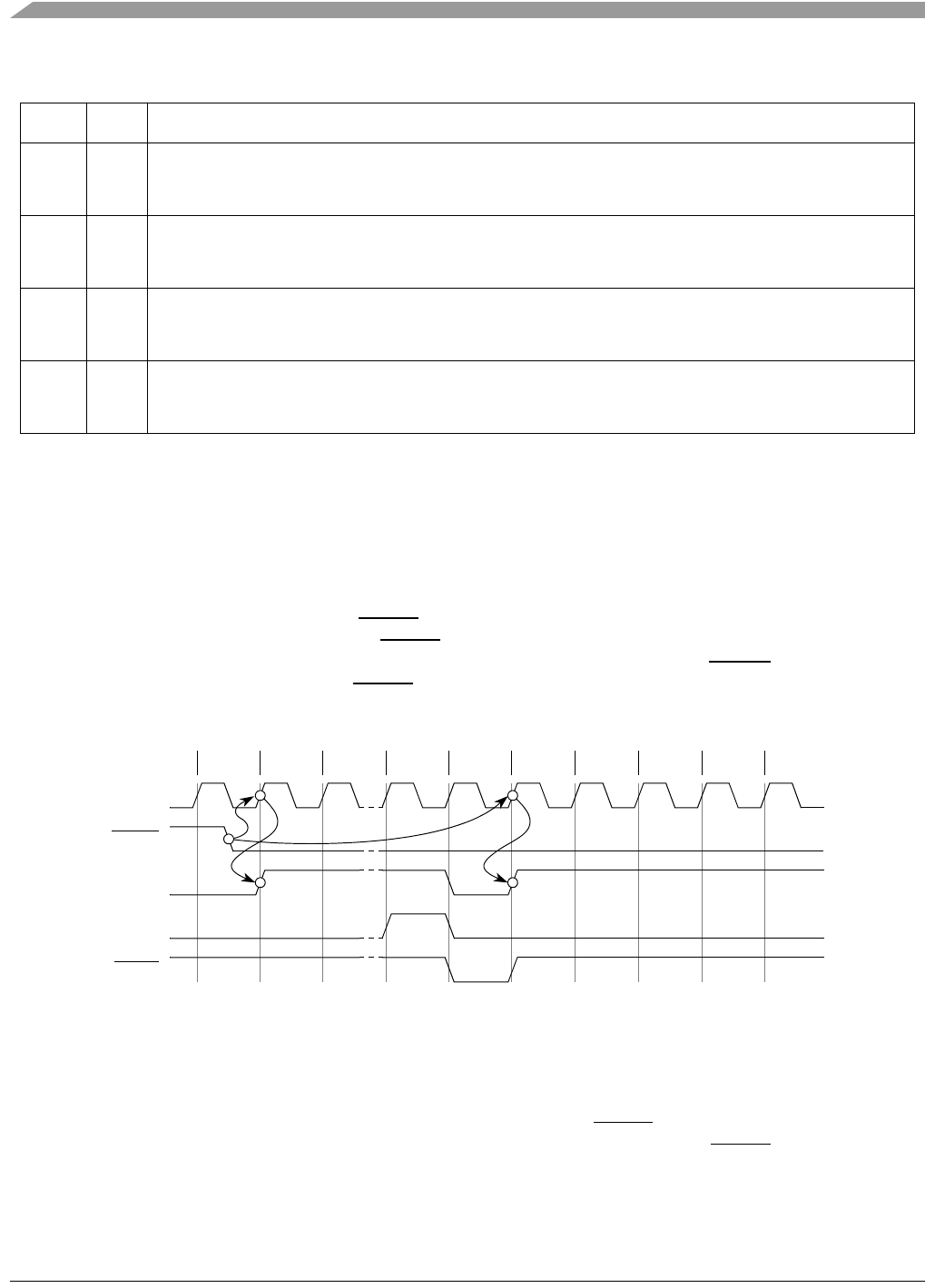
MCF548x Reference Manual, Rev. 3
24-30 Freescale Semiconductor
24.6 Timing Diagrams
The following timing diagrams show the three modes of external request operation.
24.6.1 Level-Triggered Requests
Figure 24-24 shows the timing for level-triggered external requests. For level-triggered requests, the
internal DMA request will assert when DREQ is detected low. The active high internal DMA request is
asserted on the rising edge of clock 2 after DREQ is detected low. When the DMA transfer completes, the
active high internal acknowledge is asserted (clock 4). This causes the external DACK to assert, and the
internal DMA request is negated. Since DREQ remains asserted an new internal request is signalled on the
rising edge of clock 6.
.
Figure 24-24. Level-Triggered External Request Timing
24.6.2 Edge-Triggered Requests
Figure 24-25 shows the timing for level-triggered external requests. For level-triggered requests, the
internal DMA request will assert when there is a falling edge of the DREQ signal. The active high internal
DMA request is asserted on the rising edge of clock 2 after the falling edge of DREQ. When the DMA
transfer completes, the active high internal acknowledge is asserted (clock 4). This causes the external
3 I Integer Mode
0 Fractional data representation
1 Integer data representation
2 SP Speculative Prefetch
0 Do not enable speculative prefetch
1 Enable speculive prefetch
1 CW Combined Write Enable
0 Do not enable combined writes
1 Enable combined writes
0 RL Read Line Buffer Enable
0 Do not enable line reads
1 Enable line reads
Table 24-20. Behavior of Task Table Control Bits (Continued)
Bit Name Function
CLK
DREQ
Internal DMA
Internal DMA
DACK
123456789100
Request
Acknowledge
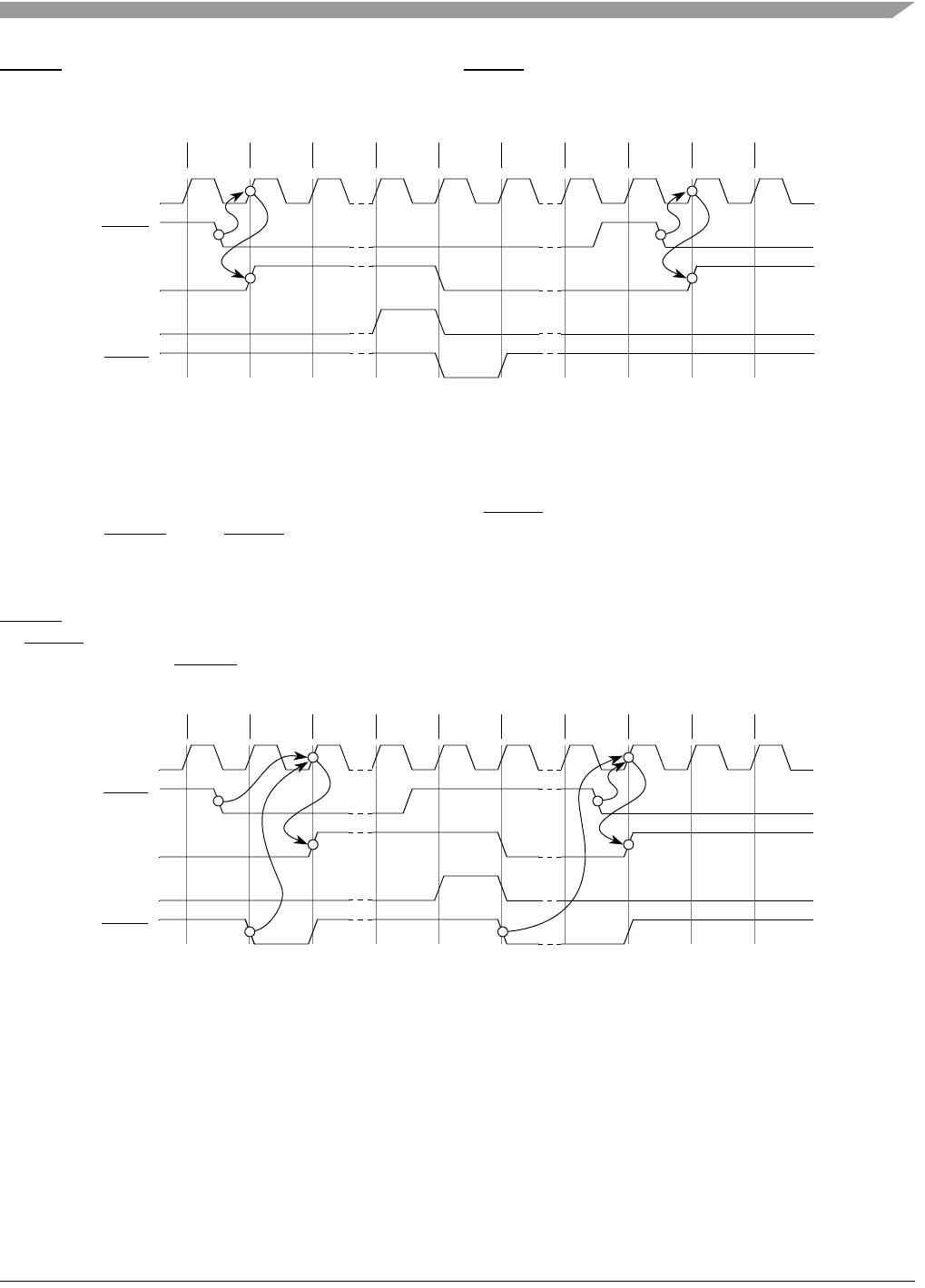
Timing Diagrams
MCF548x Reference Manual, Rev. 3
Freescale Semiconductor 24-31
DACKto assert (clock 5). The next falling edge of DREQ occurs during clock 8, causing the internal
request to assert on the rising edge of clock 9.
Figure 24-25. Edge-Triggered External Request Timing
24.6.3 Pipelined Requests
Figure 24-26 shows the timing for pipelined external requests. For pipelined requests, the internal DMA
request will assert when there is a falling edge of the DREQ signal and the previous transfer has been
completed (DACK low). DREQ goes low during clock 1. In edge-triggered mode, this would cause the
internal request to assert on the rising edge of clock 2. However, in pipelined mode the internal request
waits for the previous transfer to be acknowledged (clock 2) before the internal request is asserted on the
rising edge of clock 3. The transfer is completed and acknowledge internally during clock 5 causing
DACK to assert during clock 6. Since the transfer has already been acknowledged, the next falling edge
of DREQ (during clock 7) causes the assertion of the internal request of the following rising clock edge
(clock 8). Note that DACK is not deasserted until the new internal request asserts.
Figure 24-26. Pipelined External Requests
123456789100
CLK
DREQ
DACK
Internal DMA
Request
Internal DMA
Acknowledge
123456789100
CLK
DREQ
DACK
Internal DMA
Request
Internal DMA
Acknowledge

MCF548x Reference Manual, Rev. 3
24-32 Freescale Semiconductor
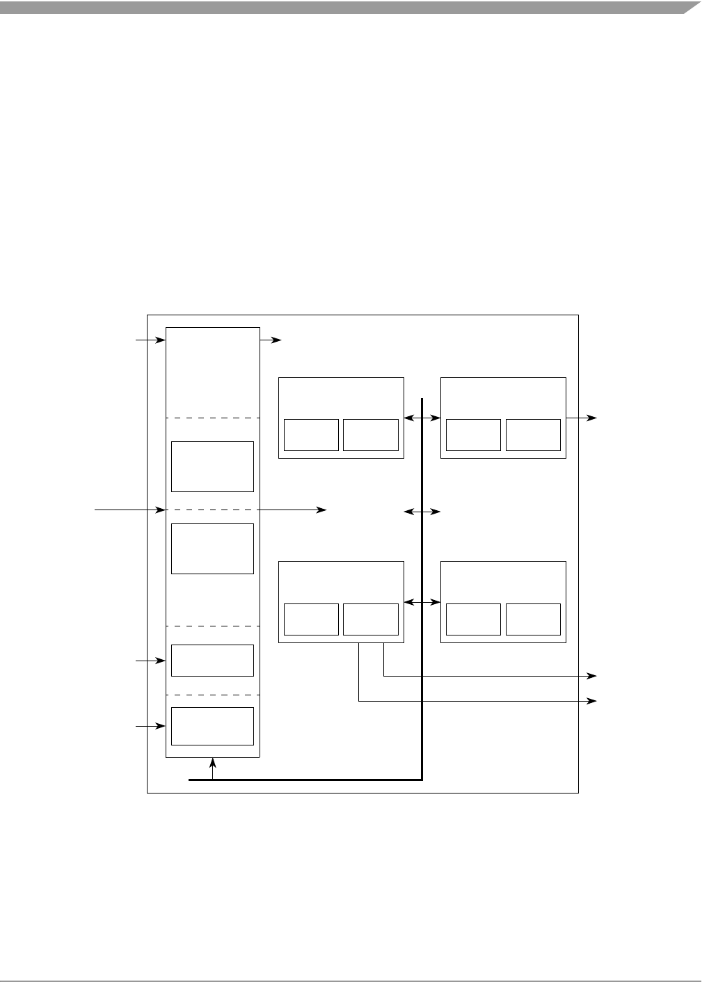
MCF548x Reference Manual, Rev. 3
Freescale Semiconductor 25-1
Chapter 25
Comm Timer Module (CTM)
25.1 Introduction
This chapter contains a detailed description of the Comm Timer Module (CTM).
25.1.1 Block Diagrams
The following section presents three block diagrams showing the CTM in greater detail. Figure 25-1 is a
high level block diagram of the CTM. The figure shows the signal flow through the sub-modules and the
architecture on a high level.
Figure 25-1. CTM High Level Block Diagram
Figure 25-2 and Figure 25-3 are conceptual block diagrams of the fixed timer channel and variable timer
channel respectively. These diagrams are more detailed than earlier diagrams but should still be considered
a conceptual illustration of the actual hardware implementations.
cAcknowledge[7:0]
cInitiator
Synchronizer
Register Timer
Variable
TimerChannel[0]
Register Timer
Fixed
TimerChannel[0]
Write/Read
Enable
Logic
Addr
Decode
Logic
8-bit
Prescaler
externalClkIn[7:0]
clk
cAcknowledge[7:0]
Register Timer
Variable
TimerChannel[n]
Register Timer
Fixed
TimerChannel[n]
•
•
•
•
•
•
•
timerInterrupt
cInitiator
Comm Timer
Module
Internal Data_bus
•
•
•
•
•
•
•
Internal
Bus
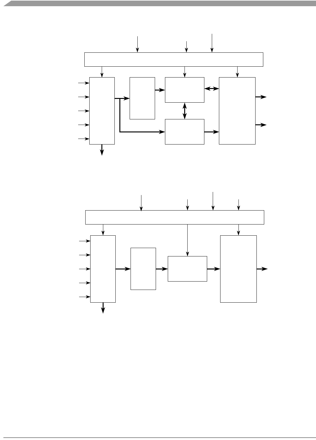
MCF548x Reference Manual, Rev. 3
25-2 Freescale Semiconductor
Figure 25-2. Fixed Timer Channel Conceptual Block Diagram
Figure 25-3. Variable Timer Channel Conceptual Block Diagram
25.1.2 Overview
The CTM module provides two functions for the communications complex. First, it can be configured to
run as a baud clock generator for the communications channels. Second, it can be used as a task initiator
for the DMA. There are three main functional blocks within the CTM that accomplish these functions: the
slave bus interface, the fixed timer channel, and the variable timer channel.
The slave bus interface to the CTM processes tasks such as the address decode, clock synchronization,
clock pre-scaling, and read/write enable decode.
mode 15-bit Percent
(High Time)
cAcknowledge
clk
Miscellaneous Block
Counter timerInterrup
t
cInitiator
Comparators
source[3:0]
percent[1:0]
counterReference[15:0]
TCRselect
dataRd[23:0]
Register
Percent
16-bit Period
Counter
Internal Bus
mode
externalClkIn
cAcknowledge
clk
Miscellaneous Block
cInitiatorComparator
source
percent[1:0]
counterReference[23:0]
TCRselect
dataRd[23:0]
Register Percent 24-bit Percent
Counter
Internal Bus

Memory Map/Register Definition
MCF548x Reference Manual, Rev. 3
Freescale Semiconductor 25-3
The fixed timer channel provides the user with two modes, a programmable baud clock generator mode or
a fixed period task initiator mode.
• In baud clock generator mode the fixed timer channel outputs a cInitiator signal that is free
running.
• In fixed period task initiator mode the fixed timer channel outputs a cInitiator signal in response
to a cAcknowledge input from the multichannel DMA’s PTD (priority task decode). It also outputs
a timerInterrupt signal to the processor if there is an error in the channel. In the current
implementation there are four fixed timer channels available.
The variable timer channel provides the user with the programmable baud clock generator mode or a
variable period task initiator mode.
• In baud clock generator mode the cInitiator output is free running.
• In variable period task initiator mode, the cInitiator output is influenced by the cAcknowledge
signal. Unlike the fixed timer channel, the variable timer channel does not have a timerInterrupt
output signal due to the variability of the period. In the current implementation there are four
variable channels available.
25.1.3 Comm Timer External Clock[7:0]
The comm timer external clock is the alternate clock signal and is provided by the user. The user must write
a 1 to CTCR[S] in the variable channel and write a 1001 to CTCR[S] within the fixed channel to select
this signal. If this signal is selected, all timing will be with respect to this clock signal. This signal is
restricted to being half the frequency or less of the system bus clock.
25.2 Memory Map/Register Definition
Section 25.2.2.1, “Comm Timer Configuration Register (CTCRn)—Fixed Timer Channel,” and
Section 25.2.2.2, “Comm Timer Configuration Register (CTCRn)—Variable Timer Channel,” explain the
registers contained within the timer module. Details are given regarding register mapping, programming
notes, bit definitions, and operating modes.
25.2.1 Timer Module Register Map
Table 25-2 shows the register mapping of the timer module.
Table 25-1. Comm Timers External Clock
Timer Channel External Signal
0TIN0
1TIN1
2TIN2
3TIN3
4 PSC3BCLK
5 PSC2BCLK
6 PSC1BCLK
7 PSC0BCLK

MCF548x Reference Manual, Rev. 3
25-4 Freescale Semiconductor
25.2.2 Register Descriptions
25.2.2.1 Comm Timer Configuration Register (CTCRn)—Fixed Timer Channel
This register provides programming options for each fixed timer channel. These channels can be
programmed to be in initiator mode or in baud clock generator mode.
Table 25-2. Timer Memory Map
Offset
(MBAR +) Name Byte 0 Byte 1 Byte 2 Byte 3 Access
0x7F00 Comm Timer Control Register 0
—Fixed Timer Channel
CTCR0 R/W
0x7F04 Comm Timer Control Register 1
—Fixed Timer Channel
CTCR1 R/W
0x7F08 Comm Timer Control Register 2
—Fixed Timer Channel
CTCR2 R/W
0x7F0C Comm Timer Control Register 3
—Fixed Timer Channel
CTCR3 R/W
0x7F10 Comm Timer Control Register 4
—Variable Timer Channel
CTCR4 R/W
0x7F14 Comm Timer Control Register 5
—Variable Timer Channel
CTCR5 R/W
0x7F18 Comm Timer Control Register 6
—Variable Timer Channel
CTCR6 R/W
0x7F1C Comm Timer Control Register 7
—Variable Timer Channel
CTCR7 R/W
31 30 29 28 27 26 25 24 23 22 21 20 19 18 17 16
RI 000000IMM PCT S
W
Reset0000000111010000
1514131211109876543210
RCRV
W
Reset1111111111111111
Reg
Addr
MBAR + 0x7F00 (CTCR0); + 0x7F04 (CTCR1); + 0x7F08 (CTCR2); + 0x7F0C (CTCR3)
Figure 25-4. Comm Timer Configuration Register (CTCRn)—Fixed Timer Channel

Memory Map/Register Definition
MCF548x Reference Manual, Rev. 3
Freescale Semiconductor 25-5
25.2.2.2 Comm Timer Configuration Register (CTCRn)—Variable Timer Channel
This register provides programming options for each variable timer channel. These channels can also be
programmed as a baud clock generator or initiator.
Table 25-3. CTCRn—Fixed Timer Channel Field Descriptions
Bits Name Description
31 I Interrupt. This bit is set whenever the timerInterrupt signal asserts in the fixed timer. This indicates
that the cAcknowledge signal has arrived too far into the current cycle to be completed within that
period or that it was too short in duration to satisfy the request. Writing a 1 will clear the bit.
0 Indicates that no interrupt has occurred or is pending.
1 Indicates that an interrupt has occurred or is pending.
30–25 — Reserved, should be cleared.
24 IM Interrupt mask. Determines if the timer interrupt will be passed on to the interrupt controller.
0 The timer interrupt is not masked. When the I bit is set, the timer interrupt will be passed to the
interrupt controller.
1 The timer interrupt is masked. The I bit will be set, but no interrupt occurs.
23 M Mode. Selects between baud clock generator mode and task initiator mode. It is set to 1 at reset.
0 Baud clock generator. In this mode, the timer output is a free running clock. Following
initialization, both timer channels react in the same way.
1 Task initiator mode. In this mode, the timer output is a bandwidth controlled initiator request signal
for the multichannel DMA. The initiator output is dependent upon the cAcknowledge signal from
the DMA. In the fixed timer channels, the percent active time is only counted while the
cAcknowledge is asserted. In contrast, the variable timer channels will count the percent active
time from beginning to end upon the first assertion of the cAcknowledge.
22–20 PCT Percent active time select. Selects the percent of the period that the cInitiator signal is asserted after
the cAcknowledge signal is received. They are set to 101 at reset.
000 100 percent
001 50 percent
010 25 percent
011 12.5 percent
100 6.25 percent
101 OFF
110–111 Reserved
19–16 S Clock enable source select. Selects the clock rate for the fixed timer channels. The clock rate for the
timer is the internal system clock divided by an 8-bit prescaler.
0000 Sysclk/1
0001 Sysclk/2
0010 Sysclk/4
0011 Sysclk/8
0100 Sysclk/16
0101 Sysclk/32
0110 Sysclk/64
0111 Sysclk/128
1000 Sysclk/256
1001 External clock
15–0 CRV Counter reference value. These 16 bits define the period of the timer i.e.: 0004 written into these
bits signifies that the period is 4 timer clock cycles long. The counter reference value is set to
0xFFFF at reset.

MCF548x Reference Manual, Rev. 3
25-6 Freescale Semiconductor
NOTE
The initiator mode is different from that of a fixed channel in that the period
is variable
.
31 30 29 28 27 26 25 24 23 22 21 20 19 18 17 16
R0 00SM PCT CRV
W
Reset0000110111111111
1514131211109876543210
RCRV
W
Reset1111111111111111
Reg
Addr
MBAR + 0x7F10 (CTCR4); + 0x7F14 (CTCR5); + 0x7F18 (CTCR6); + 0x7F1C (CTCR7)
Figure 25-5. Comm Timer Configuration Register (CTCRn)—Variable Timer Channel
Table 25-4. CTCRn—Variable Timer Channel Field Descriptions
Bits Name Description
31–29 — Reserved, should be cleared.
28 S Clock enable source select. Selects the clock rate for the fixed timer channels. The clock rate for
the timer is the internal system clock divided by an 8-bit prescaler.
0 Sysclk
1 External clock
Note: The external bus clock cannot be any faster than half the frequency of the system clock.
27 M Mode. This bit is used to select between baud clock generator mode and task initiator mode. It is
set to one 1 at reset.
1 Task initiator mode. In this mode, the timer output is a bandwidth controlled initiator request
signal for the multichannel DMA. The initiator output is dependent upon the cAcknowledge signal
from the DMA. In the fixed timer channels, the percent active time is only counted while the
cAcknowledge is asserted. In contrast, the variable timer channels will count the percent active
time from beginning to end upon the first assertion of the cAcknowledge.
0 Baud Clock Generator. In this mode, the timer output is a free running clock. Following
initialization, both timer channels react in the same way.
26-24 PCT Percent active time select. Selects the percent of the period that the cInitiator signal is asserted
after the cAcknowledge signal is received. They are set to 101 at reset.
000 100 percent
001 50 percent
010 25 percent
011 12.5 percent
100 6.25 percent
101 OFF
110–111 Reserved
23–0 CRV Counter reference value. These 24 bits define the period of the timer i.e.: 0004 written into these
bits signifies that the period is 4 timer clock cycles long. The counter reference value is set to
0xFF_FFFF at reset.

Functional Description
MCF548x Reference Manual, Rev. 3
Freescale Semiconductor 25-7
25.3 Functional Description
25.3.1 Variable Timer in Baud Clock Generator Mode
In baud clock generator mode, the functionality is the same for both fixed and variable timer channels. The
only difference is the variable timer channel has a 24-bit reference value, and the fixed channel timer only
has a 16-bit reference value.
The following equation can be used to calculate the period of the timer output:
Time-out period = (1/CTCRn[S]) × (CTCRn[CRV])
The duty cycle of the output clock is defined by CTCRn[PCT].
For example, programming the CTCR for one of the fixed channels to 0x0100_0002 will create a 50% duty
cycle output clock at half of the system clock frequency.
25.3.2 Fixed Timer in Initiator Mode
In initiator mode, the fixed timer channel can be used to create a bandwidth control initiator request signal
to the DMA. A cAcknowledge signal from the DMA is an input to the timer to indicate that the requested
task is executing. When the cAcknowledge signal asserts it activates a percent timer, thereby counting the
number of cycles the associated DMA task is active within the period. When the percent timer reaches its
timeout, the timer’s initiator output is negated so that the DMA task will not be serviced again during the
remainder of the timer period.
The fixed timeout period for the counter is determined using the same calculation used for the baud rate
generator mode:
Time-out period = (1/CTCRn[S]) x (CTCRn[CRV])
The percent counter is used to determine the number of clocks that the cAcknowledge signal from the DMA
can be asserted within the period before cInitiator is negated. Once the initiator negates, the task will stop
executing when it reaches the next boundary and will not resume until after cInitiator is asserted again at
the start of the next timer period.
The fixed timer channel can also be programmed to generate an interrupt request if the percent timer does
not timeout by the end of the timer period. The interrupt indicates that there is not enough DMA bandwidth
available for the associated task.
25.3.2.1 Fixed Timer in Initiator Mode Example
Figure 25-6 shows the initiator output generated by a fixed timer channel in initiator mode. For this
example the CTCR is programmed to 0x00A0_0010. This puts the timer in initiator mode with a timeout
period of 16 clocks and a high percentage of 25% (4 clocks).
In the first clock cycle the period counter begins to count, and the cInitiator signal is asserted. At the rising
edge of the clock in cycle 3 the cAcknowledge signal is asserted for the first time and the percent counter
begins to count.
At the rising edge of clock 5 the cAcknowledge signal is deasserted, and the percent counter stops counting
and retains a value of 0x2. The cInitiator signal remains asserted because the percent counter has not
timed out, and the period has not ended.
At the rising edge of the clock in cycle 9 the cAcknowledge signal is asserted for the second time, and the
percent counter begins to count again. At the rising edge of the clock in cycle 10 the cAcknowledge signal
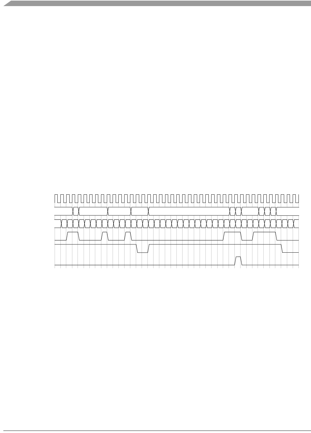
MCF548x Reference Manual, Rev. 3
25-8 Freescale Semiconductor
is deasserted, and the percent counter stops counting and retains a value of 0x3. As before the cInitiator
signal remains asserted because the percent counter has not timed out.
At the rising edge of the clock in cycle 13 the cAcknowledge signal is asserted for the third time, and the
percent counter begins to count. At the rising edge of the clock in cycle 14 the cAcknowledge signal is
deasserted, and the percent counter stops counting and retains a value of 0x4. At this time, the percent
counter has timed out. Consequently, the cInitiator signal is deasserted on the following clock. It will
remain deasserted until the beginning of the next period.
The next period begins at the rising edge of the clock in cycle 17. At that time both counters are reset to
their starting values and the cInitiator signal is asserted. At the rising edge of clock 30 the cAcknowledge
signal is asserted and remains asserted until the rising edge of clock 33. During this time the percent
counter is counting up towards its reference value.
At the rising edge of clock 32 the period counter times out while the percent counter has not reached its
reference value and is still counting. This signifies that the DMA has not been able to provide the specified
bandwidth for the selected task, and the timer interrupt signal is asserted.
At the rising edge of clock cycle 33 a new period begins. Both counters are reset; the cInitiator signal
remains asserted, and the timer interrupt is deasserted. At the rising edge of the clock in cycle 35 the
cAcknowledge is asserted and remains asserted until cycle 39. During that time, the percent counter is
counting up and times out. When it times out at the rising edge in cycle 39, the initiator deasserts on the
next clock edge. The period counter continues to count, and the periods continue on as before.
Figure 25-6. Fixed Timer Channel in Task Initiator Mode
25.3.3 Variable Timer in Initiator Mode
The variable timer channels can also be used to create bandwidth control initiator request signals for the
DMA. The functionality is similar to the fixed channel in initiator mode. The functionality varies in two
ways. First of all, the variable timer channel does not generate interrupts. Secondly, the period counter will
not start until the first time the cAcknowledge signal asserts. This means that the timer has a baseline period
(defined by the CTCR[S] and CTCR[CRV] fields), but the actual period can be greater.
25.3.3.1 Variable Timer in Initiator Mode Example
outputFor this example the CTCR is programmed to 0x00A0_0008. This puts the timer in initiator mode
with a timeout period of 8 clocks and a high percentage of 25% (2 clocks).
Unlike the fixed timer channel, the variable timer channel only has the percent counter and it does not start
counting at this point, it waits for the cAcknowledge signal to enable it.
Period
Counter Value
cAcknowledge
3 4 5 6 7 8 9 a b c d e f 10 1 2 3 4 5
CLK
6789 a b c d e f 10 1 2 3 4 5 6 7 8 92
2 3 4 5 6 7 8 9 101112131415161718192021222324252627282930313233343536373839404142
Timer Interrupt
Percent
Counter Value
cInitiator
1
00000432112000000000004000003000002
1
000000 000000
a
1
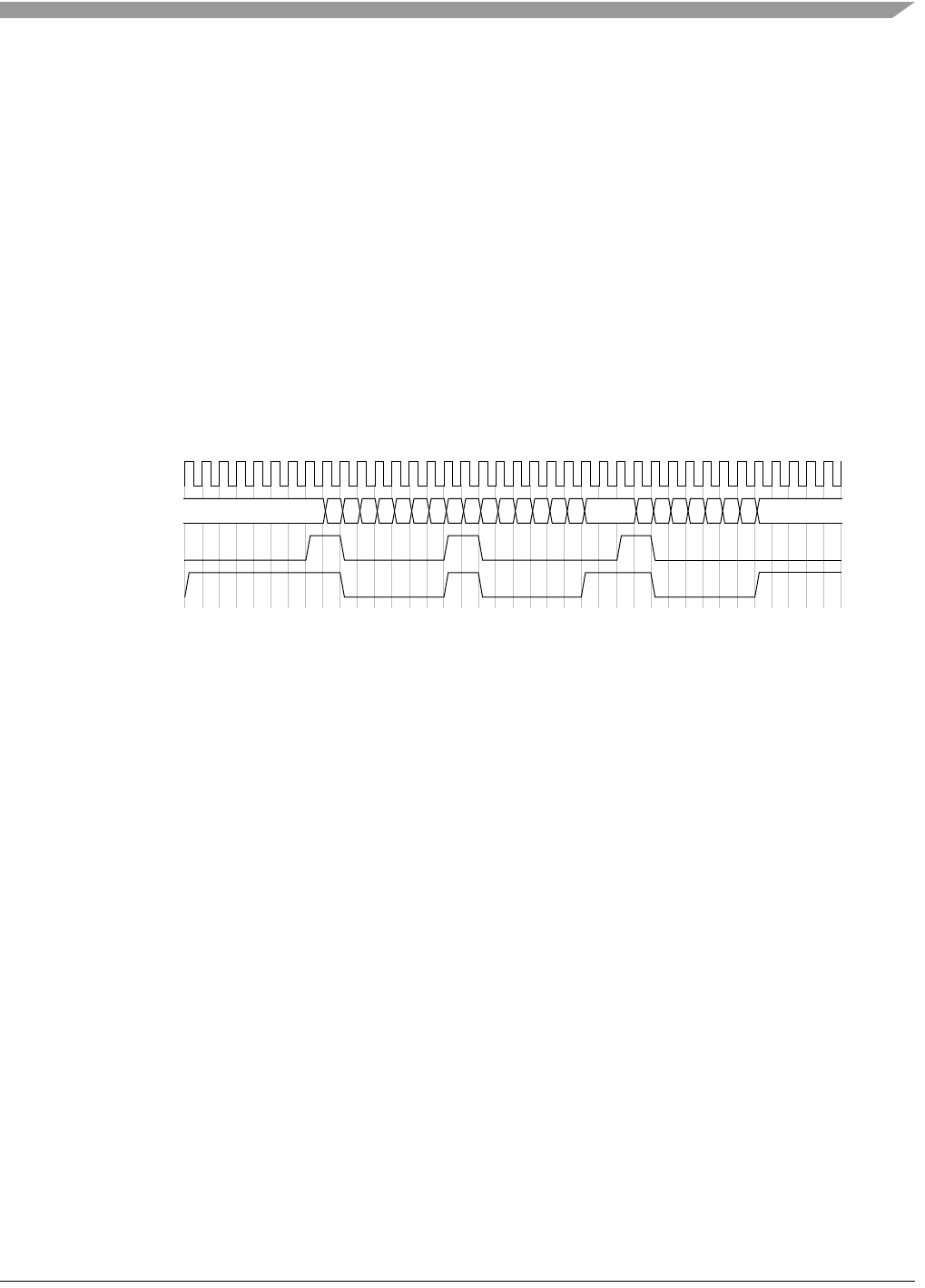
Functional Description
MCF548x Reference Manual, Rev. 3
Freescale Semiconductor 25-9
At the rising edge of the clock in cycle 8, the cAcknowledge signal is asserted. At that point the percent
counter begins to count. At the rising edge of clock 10, cAcknowledge is deasserted and the counter reaches
the high time value. As a result of the counter reaching the high time value (2), cInitiator is deasserted.
The counter does not stop counting; however, it continues to count toward the period reference value (8).
At the rising edge of clock 16, the timer has timed out, it is reset to its initial value (1), and the cInitiator
signal is asserted.
The next two periods act in a similar fashion. What is most important to be aware of in this diagram is the
fact that, unlike the fixed timer channel, the variable timer does not have a fixed period. The percent
counter only begins counting when cAcknowledge has arrived. It counts to the period value then resets and
waits again.
The first period is from clock 1 to clock 16 or 15 clock cycles. The second period is only 8 cycles long and
is from clock 16 to clock 24. The third cycle is 10 cycles long running from clock 24 to 34.
The final period is somewhat undefined as the cAcknowledge signal has not been asserted yet. Therefore,
it is at least 13 cycles long and can be any value greater than that.
Figure 25-7. Variable Timer Channel in Initiator Mode
Percent
Counter Value
cAcknowledge
2 3 4 5 6 7 8 1 2 3 4 5 6
CLK
7 8 2 3 4 5 6 7 8
2 3 4 5 6 7 8 9 10 11 12 13 14 15 16 17 18 19 20 21 22 23 24 25 26 27 28 29 30 31 32 33 34 35 36 37 38
cInitiator
1
000001 000001 000001

MCF548x Reference Manual, Rev. 3
25-10 Freescale Semiconductor
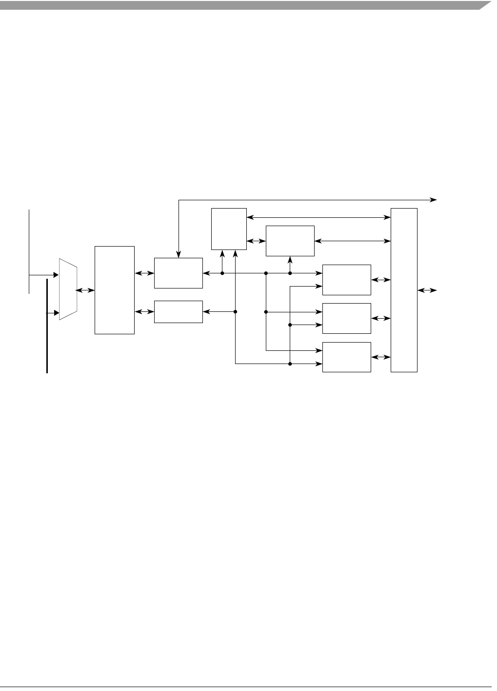
MCF548x Reference Manual, Rev. 3
Freescale Semiconductor 26-1
Chapter 26
Programmable Serial Controller (PSC)
26.1 Introduction
This chapter describes the MCF548x programmable serial controller (PSC).
26.1.1 Block Diagram
A block diagram of the PSC/IrDA module is shown in Figure 26-1 below.
Figure 26-1. PSC/IrDA Block Diagram
26.1.2 Overview
The PSC/IrDA module provides asynchronous, synchronous, and IrDA 1.1 compliant receiver/transmitter
serial communications. Each receiver and transmitter contains a 512-byte FIFO to reduce interrupt
overhead.
The MCF548x contains four programmable serial controllers.
26.1.3 Features
The primary features of the PSC/IrDA module are as follows:
• Full duplex receiver and transmitter in all modes
• Seven operation modes (UART, three soft modem modes, and three IrDA modes)
• Two 512-byte FIFOs
26.1.4 Modes of Operation
The operation modes supported by the PSC/IrDA module are as follows.
• Universal asynchronous receiver transmitter (UART) mode
Soft
MIR
FIR
SIR
UART
Modem
Serial
MUX
Bus
Control
Registers
FIFOs
Modem
CODEC
CODEC
CODEC
Interface
Comm Bus
Control
Mux
Ports
IP Bus

MCF548x Reference Manual, Rev. 3
26-2 Freescale Semiconductor
• Backward compatible with the MC68681
— 5,6,7,8 bits data plus parity
— Odd, even, none, or force parity
— Stop bit width programmable in 1/16 bit increments
— Parity, framing, and overrun error detection
— Automatic PSCnCTS and PSCnRTS modem control signals
• IrDA 1.0 SIR mode (SIR)
— Baud rate range: 2400 to 115200 bps
— Selectable pulse width: either 3/16 bit duration or 1.6 us.
• IrDA 1.1 MIR mode (MIR)
— Baud rate: 0.576 Mbps or 1.152 Mbps.
• IrDA 1.1 FIR mode (FIR)
— Baud rate: 4.0 Mbps
• 8-bit soft modem mode (modem8)
• 16-bit soft modem mode (modem16)
• AC97 soft modem mode (AC97)
The three soft modem modes (modem8, modem16, and AC97) are jointly referred to as “modem mode.”
The three IR modes (SIR, MIR, and FIR) are jointly referred to as “IrDA mode.”
26.2 Signal Description
26.2.1 PSCnCTS/PSCBCLK
These signals either operate as the clear to send input signals in UART mode or the bit clock input signals
in modem modes and IrDA modes. Please refer to ,” for information about how to program this signal
function.
In MIR and FIR mode, the frequency is a multiple of the input bit clock frequency, and the bit clock
frequency should be within +/-0.1% and +/-0.01% of the ideal one, respectively.
26.2.2 PSCnRTS/PSCFSYNC
These signals act as transmitter request to send output in UART mode, the frame sync input in modem8
and modem16 modes, or the RTS output (which acts as frame sync) in AC97 modem mode.
Refer to the Chapter 15, “GPIO,” and Section 26.3.3.5, “Command Register (PSCCRn),” for information
about how to program this signal function.
26.2.3 PSCnRXD
PSCnRXD are the receiver serial data inputs for the PSC modules. When the PSC clock is stopped for
power-down mode, any transition on the signals restarts them.

Memory Map/Register Definition
MCF548x Reference Manual, Rev. 3
Freescale Semiconductor 26-3
26.2.4 PSCnTXD
PSCnTXD are the transmitter serial data outputs for the PSC modules. The output is held high (mark
condition) when the transmitter is disabled, idle, or in the local loopback mode. The PSCnTXD signals can
be programmed to be driven low (break status) by a command.
Refer to Section 26.3.3.5, “Command Register (PSCCRn),” for information about how to program this
signal function.
26.2.5 Signal Properties in Each Mode
The following table summarizes the signals used for serial communications.
26.3 Memory Map/Register Definition
26.3.1 Overview
This section provides a detailed description of all memory locations and registers. Note that the meaning
of some control register fields depends on the operation mode.
26.3.2 Module Memory Map
The names and address locations of all control registers are listed in Table 26-2.
.
Table 26-1. PSC Signal Properties
Signal Name I/O UART Modem8
Modem16 AC97 SIR MIR
FIR
PSCBCLK I — Bit clock — xN bit clock
PSCFSYNC I — Sync — — —
PSCnTXD O Serial transmit data
PSCnRXD I Serial receive data
PSCnRTS O Transmitter request
to send or Receiver
ready to receive
— Frame sample
sync (48 kHz)
——
PSCnCTS I Transmitter clear to
send
————
Table 26-2. PSC Memory Map
MBAR Offset
Name Byte0 Byte1 Byte2 Byte3
Access
PSC0 PSC1 PSC2 PSC3
0x8600 0x8700 0x8800 0x8900 PSC Mode register 1, 2 PSCMR1,
PSCMR2
—R/W
0x8604 0x8704 0x8804 0x8904 PSC Status Register PSCSR — R
PSC Clock Select Register PSCCSR — W
0x8608 0x8708 0x8808 0x8908 PSC Command Register PSCCR – W

MCF548x Reference Manual, Rev. 3
26-4 Freescale Semiconductor
0x860C 0x870C 0x880C 0x890C PSC Receive Buffer PSCRB R
PSC Transmit Buffer PSCTB W
0x8610 0x8710 0x8810 0x8910 PSC Input Port Change Register PSCIPCR — R
PSC Auxiliary Control Register PSCACR —W
0x8614 0x8714 0x8814 0x8914 PSC Interrupt Status Register PSCISR — R
PSC Interrupt Mask Register PSCIMR — W
0x8618 0x8718 0x8818 0x8918 PSC Counter Timer Upper Register PSCCTUR — R/W
0x861C 0x871C 0x881C 0x891C PSC Counter Timer Lower Register PSCCTLR — R/W
0x8620
–0x863
0
0x8720
–0x873
0
0x8820
–
0x8830
0x8920
–
0x8930
Reserved
0x8634 0x8734 0x8834 0x8934 PSC Input Port PSCIP — R
0x8638 0x8738 0x8838 0x8938 PSC Output Port Set PSCOPSET — W
0x863C 0x873C 0x883C 0x893C PSC Output Port Reset PSCOP
RESET
—W
0x8640 0x8740 0x8840 0x8940 PSC PSC / IrDA Control Register PSCSICR — R/W
0x8644 0x8744 0x8844 0x8944 PSC IrDA Control Register 1 PSCIRCR1 — R/W
0x8648 0x8748 0x8848 0x8948 PSC IrDA Control Register 2 PSCIRCR2 — R/W
0x864C 0x874C 0x884c 0x894C PSC IrDA SIR Divide Register PSCIRSDR — R/W
0x8650 0x8750 0x8850 0x8950 PSC IrDA MIR Divide Register PSCIRMDR — R/W
0x8654 0x8754 0x8854 0x8954 PSC IrDA FIR Divide Register PSCIRFDR — R/W
0x8658 0x8758 0x8858 0x8958 PSC RxFIFO Counter Register PSCRFCNT — R
0x865C 0x875C 0x885C 0x895C PSC TxFIFO Counter Register PSCTFCNT — R
0x8660 0x8760 0x8860 0x8960 PSC RxFIFO Data Register PSCRFDR R/W
0x8664 0x8764 0x8864 0x8964 PSC RxFIFO Status Register PSCRFSR — R
0x8668 0x8768 0x8868 0x8968 PSC RxFIFO Control Register PSCRFCR — R/W
0x866E 0x876E 0x886E 0x896E PSC RxFIFO Alarm Register — PSCRFAR R/W
0x8672 0x8772 0x8872 0x8972 PSC RxFIFO Read Pointer — PSCRFRP R/W
0x8676 0x8776 0x8876 0x8976 PSC RxFIFO Write Pointer — PSCRFWP R/W
0x867A 0x877A 0x887A 0x897A PSC RxFIFO Last Read Frame
Pointer
— PSCRLRFP R/W
0x867E 0x877E 0x887E 0x897E PSC RxFIFO Last Write Frame
Pointer
— PSCRLWFP R/W
0x8680 0x8780 0x8880 0x8980 PSC TxFIFO Data Register PSCTFDR R/W
0x8684 0x8784 0x8884 0x8984 PSC TxFIFO Status Register PSCTFSR — R
0x8688 0x8788 0x8888 0x8988 PSC TxFIFO Control Register PSCTFCR — R/W
Table 26-2. PSC Memory Map (Continued)
MBAR Offset
Name Byte0 Byte1 Byte2 Byte3
Access
PSC0 PSC1 PSC2 PSC3

Memory Map/Register Definition
MCF548x Reference Manual, Rev. 3
Freescale Semiconductor 26-5
26.3.3 Register Descriptions
This section gives detailed descriptions of the user accessible registers and bits within the module. In cases
where the operation mode affects the functionality of the control register, the operation in each mode is
described.
NOTE
Bit functions can vary in different operating modes. The field descriptions
are labelled to indicate which modes use a particular field.
26.3.3.1 Mode Register 1(PSCMR1n)
PSCMR1 controls some of the module configurations. It can be read or written at any time. It is accessed
when the mode register pointer points to PSCMR1. The pointer is set to mode register 1 by reset or by a
set pointer command using the MISC[2:0] bits in the command register (PSCCR). The pointer points to
the next mode register, PSCMR2, after reading or writing PSCMR1.
0x868E 0x878E 0x888E 0x898E PSC TxFIFO Alarm Register — PSCTFAR R/W
0x8692 0x8792 0x8892 0x8992 PSC TxFIFO Read Pointer — PSCTFRP R/W
0x8696 0x8796 0x8896 0x8996 PSC TxFIFO Write Pointer — PSCTFWP R/W
0x869A 0x879A 0x889A 0x899A PSC TxFIFO Last Read Frame
Pointer
— PSCTLRFP R/W
0x869E 0x879E 0x889E 0x899E PSC TxFIFO Last Write Frame
Pointer
— PSCTLWFP R/W
76543210Mode
R RXRTS RXIRQ /
FU
ERR PM PT BC UART
W
R0RXIRQ000000
All other
modes
W
Reset00100000
Reg
Addr
MBAR + 0x8600 (PSC0); 0x8700 (PSC1); 0x8800 (PSC2); 0x8900 (PSC3)
Figure 26-2. PSC Mode Register 1 (PSCMR1n)
Table 26-2. PSC Memory Map (Continued)
MBAR Offset
Name Byte0 Byte1 Byte2 Byte3
Access
PSC0 PSC1 PSC2 PSC3

MCF548x Reference Manual, Rev. 3
26-6 Freescale Semiconductor
26.3.3.2 Mode Register 2 (PSCMR2n)
PSCMR2 controls some of the module configuration. It is accessed when the mode register pointer points
to PSCMR2, which occurs after any access to PSCMR1. Access to PSCMR2 does not change the pointer.
The pointer is set to the mode register 1 by reset or by a set pointer command using the MISC[2:0] bits in
the command register (PSCCR).
Table 26-3. PSCMR1n Field Descriptions
Bits Name Description
7 RXRTS Receiver request-to-send (UART and SIR modes only). Allows the PSCnRTS output to control the
PSCnCTS input of the transmitting device to prevent receiver overrun. If both the receiver and
transmitter are incorrectly programmed for PSCnRTS control, PSCnRTS control is disabled for
both. Transmitter RTS control is configured in PSCMR2n[TxRTS].
0 The receiver has no effect on PSCnRTS.
1 When a valid start bit is received, PSCnRTS is negated if the UART's FIFO is full. PSCnRTS is
reasserted when the FIFO has an empty position available.
6RXIRQ/
FU
Receiver interrupt select (all modes).
0 RxRDY is the source that generates IRQ or DMA request.
1 FU is the source that generates IRQ or DMA request.
5 ERR Error mode (UART mode only). Configures the FIFO status bits, USRn[RB,FE,PE].
0 Character mode. The PSCSRn values reflect the status of the character at the top of the FIFO.
ERR must be 0 for correct A/D flag information when in multidrop mode.
1 Block mode. The PSCSRn values are the logical OR of the status for all characters reaching the
top of the FIFO since the last RESET ERROR STATUS command for the channel was issued. See
Section 26.3.3.5, “Command Register (PSCCRn).”
This bit is fixed to 1. It is provided for compatibility with previous implementations.
4–3 PM Parity mode (UART mode only). Selects the parity or multidrop mode for the channel. The parity
bit is added to the transmitted character, and the receiver performs a parity check on incoming
data. The value of PM affects PT, as shown in the table displayed below in the PT field description.
2 PT Parity type (UART mode only). PM and PT together select parity type (PM = 0x) or determine
whether a data or address character is transmitted (PM = 11).
1–0 BC Bits per character (UART mode only). Select the number of data bits per character to be sent. The
values shown do not include start, parity, or stop bits.
00 5 bits
01 6 bits
10 7 bits
11 8 bits
PM Parity Mode Parity Type
(PT= 0)
Parity Type
(PT= 1)
00 With parity Even parity Odd parity
01 Force parity Low parity High parity
10 No parity n/a
11 Multidrop mode Data character Address
character

Memory Map/Register Definition
MCF548x Reference Manual, Rev. 3
Freescale Semiconductor 26-7
76543210 Mode
R CM TXRTS TXCTS SB UART
W
RCM TXRTSTXCTS0000 SIR
W
RCM 000000All other modes
W
Reset00000000
Reg
Addr
MBAR + 0x8600 (PSC0); 0x8700 (PSC1); 0x8800 (PSC2); 0x8900 (PSC3)
Figure 26-3. PSC Mode Register 2 (PSCMR2n)
Table 26-4. PSCMR2n Field Descriptions
Bits Name Description
7–6 CM Channel mode (all modes). Selects a channel mode. Section 26.4.10, “Looping Modes,” describes
individual modes.
00 Normal
01 Automatic echo
10 Local loop-back
11 Remote loop-back
5 TXRTS Transmitter ready-to-send (UART and SIR modes). Controls negation of PSCnRTS to automatically
terminate a message transmission. Attempting to program a receiver and transmitter in the same
channel for PSCnRTS control is not permitted and disables PSCnRTS control for both.
0 The transmitter has no effect on PSCnRTS.
1 In applications where the transmitter is disabled after transmission completes, setting this bit
automatically clears PSCOP[RTS] one bit time after any characters in the channel transmitter shift
and holding registers are completely sent, including the programmed number of stop bits.

MCF548x Reference Manual, Rev. 3
26-8 Freescale Semiconductor
26.3.3.3 Status Register (PSCSRn)
The PSCSR register indicates the status of the characters in the FIFO and the status of the transmitter and
receiver.
4 TXCTS Transmitter clear-to-send (UART and SIR modes). If both TxCTS and TxRTS are enabled, TxCTS
controls the operation of the transmitter.
0 PSCnCTS has no effect on the transmitter.
1 Enables clear-to-send operation. The transmitter checks the state of PSCnCTS each time it is ready
to send a character. If PSCnCTS is asserted, the character is sent; if it is negated, the channel
PSCnTXD remains in the high state and transmission is delayed until PSCnCTS is asserted.
Changes in PSCnCTS as a character is being sent do not affect its transmission.
3–0 SB Stop-bit length control (UART mode only). Selects the length of the stop bit appended to the transmitted
character. Stop-bit lengths of 9/16th to 2 bits are programmable for 6–8 bit characters. Lengths of 1
1/16th to 2 bits are programmable for 5-bit characters. In all cases, the receiver checks only for a high
condition at the center of the first stop-bit position, that is, one bit time after the last data bit or after the
parity bit, if parity is enabled.
If an external 1x clock is used for the transmitter, clearing bit 3 selects one stop bit and setting bit 3
selects two stop bits for transmission.
An external clock source can be used to generate the baud rate. This is done by configuring the
communications timer. Please refer to the about external clock sources. Also refer to Table 26-6.
15 14 13 12 11 1098 7 6543210
RRB_
NEOF
FE_
PHYERR
PE_
CRCERR
OE TXEMP_
URERR
TX
RDY
FU RX
RDY
CDE_
DEOF
ERR 0 0 0 0 0 0
W
Reset0 0 0 0 0 000 0 0000000
Reg
Addr
MBAR + 0x8604 (PSC0); 0x8704 (PSC1); 0x8804(PSC2); 0x8904 (PSC3)
Figure 26-4. PSC Status Register (PSCSRn)
Table 26-4. PSCMR2n Field Descriptions
Bits Name Description
SB 5
Bits
6–8
Bits
SB 5 Bits 6–8
Bits
SB 5–8
Bits
SB 5–8
Bits
0000 1.063 0.563 0100 1.313 0.813 1000 1.563 1100 1.813
0001 1.125 0.625 0101 1.375 0.875 1001 1.625 1101 1.875
0010 1.188 0.688 0110 1.438 0.938 1010 1.688 1110 1.938
0011 1.250 0.750 0111 1.500 1.000 1011 1.750 1111 2.000

Memory Map/Register Definition
MCF548x Reference Manual, Rev. 3
Freescale Semiconductor 26-9
Table 26-5. PSCSRn Field Descriptions
Bits Name Description
15 RB_NEOF For UART and SIR modes, this field signifies a received break.
0 No break received.
1 Break received.
For modem mode, this field is reserved.
In MIR and FIR mode, this bit signifies a next byte is EOF.
0 The next byte to be read from the RxFIFO is not the last one of the frame.
1 The next byte to be read from the RxFIFO is the last one of the frame. This bit is effective when
RxRDY = 1.
14 FE_PHYERR For UART and SIR modes, this field signifies a framing error.
0 No error.
1 The stop bits are not correct.
In modem mode, this bit is reserved.
In MIR and FIR mode, this bit signifies a Physical layer error.
0 No error
1 In MIR mode, this denotes that the receiver received an abort. In FIR mode, this denotes that
there was a decode error. This bit can be cleared by the reset error status command in the
PSCCR.
13 PE_CRCERR For UART and SIR modes, this field signifies a parity error.
0 Parity error has not occurred.
1 Parity error has occurred.
In modem mode, this bit is reserved.
In MIR and FIR mode, this bit signifies a CRC error.
0 No error
1 The CRC value was not correct. This bit can be cleared by the reset error command in the
PSCCR.
12 OE For all modes, this field signifies an overrun error occurred.
0 No error.
1 One or more received characters have been lost. This bit is cleared by the reset error command
in CR.
11 TXEMP_
URERR
For UART and SIR modes, this field signifies a transmitter empty.
0 The transmitter is busy or there is at least one data in the TxFIFO.
1 The transmitter and the TxFIFO is empty.
In modem and MIR and FIR modes, this bit signifies an underrun error.
0 No error.
1 Underrun error occurred. When the transmitter intended to send, there was no data in the
TxFIFO. This bit is cleared by the reset error command in the PSCCR.
10 TXRDY For all modes, this field signifies a Transmitter ready.
0 The number of the data in the TxFIFO is more than the threshold. Different from FIFO’s alarm,
this bit is determined only by the threshold and not by the granularity.
1 The number of data in the TxFIFO is less than or equal to the threshold (TFALARM). In UART
and SIR mode, this bit becomes asserted only when the transmitter is enabled. On the contrary,
in modem mode and MIR and FIR IrDA mode, this bit becomes asserted even if the transmitter
is disabled.

MCF548x Reference Manual, Rev. 3
26-10 Freescale Semiconductor
26.3.3.4 Clock Select Register (PSCCSRn)
The comm timers (CTMs) or the PSC’s timer (see Section 26.3.3.11, “Counter Timer Registers
(PSCCTURn, PSCCTLRn)” for more information) can be used to generate the baud rate for UART and
SIR modes. The PSCCSR selects which clock input is used to generate the baud rate. The system clock
can be selected or the output from one of the comm timers (CTM) can be selected. If the CTM clock is
selected, it can be divided by 1 or 16. Please refer to the Chapter 25, “Comm Timer Module (CTM),” for
more information on the clock sources for baud rate generation.
Figure 26-5 shows the clock options for generating the baud rate for UART or SIR modes.
Figure 26-5. UART and SIR Baud Rate Clocking Sources
9 FU For all modes, this field signifies that the RxFIFO is full.
0 The number of data in the RxFIFO is less than the threshold or the number of data is more than
the granularity after exceeding the threshold.
1 The number in RxFIFO is more than the threshold. This bit becomes low after reading enough
data from RxFIFO and the number in it becomes less than the granularity.
8 RXRDY For all modes, this field signifies a Receiver ready.
0 There is no data in the RxFIFO.
1 There is at least one data in the RxFIFO.
7 CDE_DEOF In UART mode, this bit is reserved.
In modem and SIR mode, this bit is reserved.
In MIR and FIR mode, this bit signifies Detect End of Frame or the RxFIFO contains EOF.
0 The receiver has not received an EOF after the last read PSCSR command and there is no EOF
in the FIFO.
1 The receiver has received an EOF since last PSCSR read or there is at least one EOF in the
RxFIFO. In this case, the interrupt and request can be asserted even if the number of the RxFIFO
is less than the threshold and PSCMR1[6]=1. This bit is also set if an error occurred and no
correct EOF is received.
6 ERR Error bit. OR of all errors status bits including FIFO errors.
0 No error was detected.
1 At least one error occurred
5 - 0 — Reserved
Table 26-5. PSCSRn Field Descriptions (Continued)
Bits Name Description
Comm
×1
Prescaler
×16
Prescaler
Clock
Generator
16-Bit
Divider ×32
Prescaler
TCSEL or RCSEL
Timern
Baud Rate
Internal
Bus
Clock

Memory Map/Register Definition
MCF548x Reference Manual, Rev. 3
Freescale Semiconductor 26-11
The upper 4 bits set the receiver and the lower 4 bits set the transmitter clock source. To use the system
bus clock for both the transmitter and receiver, program the PSCCSR with 0xDD. It is possible to program
the transmitter and the receiver with different clock sources.
26.3.3.5 Command Register (PSCCRn)
The PSCCR is used to supply commands to the PSC. Multiple commands can be specified in a single write
to the PSCCR if the commands are not conflicting. For example, reset transmitter and enable transmitter
commands cannot be specified in a single command.
76543210
R
WRCSEL TCSEL
Reset11011101
Reg
Addr
MBAR + 0x8604 (PSC0); 0x8704 (PSC1); 0x8804 (PSC2); 0x8904 (PSC3)
Figure 26-6. Clock Select Register (PSCCSRn)
Figure 26-7. PSCCSRn Field Descriptions
Bits Name Description
7–4 RCSEL In UART or SIR mode, this is the receiver clock select. Table 26-6 shows the bit settings for this field.
In all other modes, this field is reserved.
3–0 TCSEL In UART or SIR mode, this is the transmitter clock select. Tabl e 26-6 shows the bit settings for this field.
In all other modes, this field is reserved.
Table 26-6. RCSEL[3:0] and TCSEL[3:0]
RCSEL[3:0] or
TCSEL[3:0] UART Mode SIR Mode
0000 – 1101 System Bus
Clock
System Bus
Clock
1110 × 16 CTM clock
× 16 CTM clock
1111 × 1 CTM clock
76543210
R0
WMISC TXC RXC
Reset00000000
Reg
Addr
MBAR + 0x8608 (PSC0); 0x8708 (PSC1); 0x8808(PSC2); 0x8908 (PSC3)
Figure 26-8. PSC Command Register (PSCCRn)

MCF548x Reference Manual, Rev. 3
26-12 Freescale Semiconductor
Table 26-7. PSCCRn Field Descriptions
Bits Value Command Description
7 — Reserved, should be cleared.
6–4 MISC Field (This field selects a single command.)
000 NO COMMAND —
001 RESET MODE
REGISTER
POINTER
Causes the mode register pointer to point to PSCMR1n.
010 RESET
RECEIVER
The receiver and RxFIFO are immediately reset. The receiver is disabled. The FU and RxRDY
bits in the PSCSR are cleared and RxFIFO is initialized. All other registers are unaltered.
011 RESET
TRANSMITTER
The transmitter and TxFIFO immediately reset. The transmitter is disabled.
• In UART and SIR mode, the TxEMP and TxRDY bits in PSCSR are cleared.
• In modem, MIR and FIR mode, the URERR bit is not cleared and the TxRDY is asserted due
to no holding data in TxFIFO.
100 RESET ERROR
STATUS
• In UART and SIR mode, the RB, FE_CDE (FE in SIR mode), PE and OE bits in PSCSR are
cleared.
• In modem mode, the OE and URERR are cleared.
• In MIR and FIR mode, the PHYERR, CRCERR, OE and URERR are cleared.
101 RESET
BREAK–
CHANGE
INTERRUPT
The delta break bit, DB, in PSCISR is cleared. This command has no effect in modem, MIR and
FIR mode.
110 START BREAK This command forces PSCnTXD port low. If the transmitter is empty, the start of the break
conditions can be delayed up to one bit time. If the transmitter is active, the break begins when
the transmission of the character is completed. If a character is in the transmitter shift register, the
start of the break delayed until the character is transmitted. If the TxFIFO has a character, the
character is transmitted after the break. The transmitter must be enabled for this command to be
accepted. The state of the PSCnCTS input port is ignored for this command.
This command has no effect in modem, MIR, and FIR mode.
111 STOP BREAK This command causes PSCnTXD to go high (mark) with two bit times. If there are any characters
stored in the TxFIFO, they are transmitted. This command has no effect in modem, MIR, and FIR
mode.

Memory Map/Register Definition
MCF548x Reference Manual, Rev. 3
Freescale Semiconductor 26-13
3–2 TXC Field (This field selects a single command)
00 NO ACTION
TAKEN
The transmitter stays in its current mode.
01 TRANSMITTER
ENABLE
This command enables operation of the transmitter. If the transmitter is already enabled, this
command has no effect.
• In UART and SIR mode, the TxEMP and TxRDY bits in PSCSR are also asserted.
• In modem, MIR and FIR mode, TxFIFO can be loaded while the transmitter is disabled unlike
UART and SIR mode. Therefore TxRDY behaves the same whether the transmitter is enabled
or not, and is not automatically set when the transmitter is enabled. The URERR bit is also not
automatically set by enabling the transmitter.
• In modem8 and modem16 mode, if no data has been written into the TxFIFO before getting the
first frame sync after enabling the transmitter, URERR will be set.
• In AC97 mode, URERR will be set if
-- the TxFIFO is empty and the transmitter is enabled and
-- the ‘Codec Ready’ condition has been detected by the receiver and
-- a frame sync occurs before any samples have been written into the TxFIFO.
10 TRANSMITTER
DISABLE
This command terminates transmitter operation. If the transmitter is already disabled, this
command has no effect.
• In UART and SIR mode, the TxEMP and TxRDY bits are negated.
• In modem, MIR and FIR mode, the TxRDY bit remains as the current condition.
• In UART, modem and SIR mode, if a character is being transmitted when the transmitter
becomes disabled, the transmission of the character is completed before the transmitter
becomes inactive.
• In MIR and FIR mode, if the transmitter is sending and there are any characters in the TxFIFO
when the transmitter becomes disabled, the transmitter continues sending data until the last
byte (data with EOF mark) in the current frame.
11 — Reserved, do not use.
Table 26-7. PSCCRn Field Descriptions (Continued)
Bits Value Command Description

MCF548x Reference Manual, Rev. 3
26-14 Freescale Semiconductor
26.3.3.6 Receiver Buffer (PSCRBn) and Transmitter Buffer (PSCTBn)
Data is read from the Rx FIFO by reading from the read-only PSCRBn registers. Data is written to the Tx
FIFO by writing to the write-only PSCTBn registers.
Figure 26-9 shows the registers for UART, Modem 8, SIR, MIR, and FIR modes. Figure 26-10 shows the
registers for Modem 16 mode. Figure 26-11 shows the registers for AC97 mode.
NOTE
The Rx and Tx FIFOs can also be accessed via the PSCRFDRn and
PSCTFDRn registers. The Tx FIFO access via the PSCTBn will be blocked
if the PSC is in UART or SIR mode and the transmitter is disabled.
However, access via PSCTFDRn will never be blocked. See
Section 26.3.3.22, “Rx and Tx FIFO Data Register (PSCRFDRn,
PSCTFDRn)” for more information.
1–0 RXC Field (This field selects a single command)
00 NO ACTION
TAKEN
The receiver stays in its current mode.
01 RECEIVER
ENABLE
This command enables operation of the receiver. If the receiver is already enabled, this command
has no effect.
• In UART mode, if the parity mode is not multidrop mode, this command enables the receiver
and forces the receiver to search for start bit state. If in multidrop mode, the receiver
continuously monitors the received data regardless of whether it is enabled or not.
10 RECEIVER
DISABLE
This command disables the receiver immediately. This command has no effect if the receiver is
already disabled.
• In UART and SIR mode, a character being received when the receiver becomes disabled is
lost.
• However, in modem mode, if a character is being received when the receiver becomes
disabled, the reception of the character is completed before the receiver is disabled.
• Similarly, in MIR and FIR mode, the receiver continues to receive the input serial data until it
finishes receiving the current frame.
If the PSC is programmed to operate in local loopback mode or UART multidrop mode, the
receiver operates even though this command is selected.
11 — Reserved, do not use.
Table 26-7. PSCCRn Field Descriptions (Continued)
Bits Value Command Description

Memory Map/Register Definition
MCF548x Reference Manual, Rev. 3
Freescale Semiconductor 26-15
Figure 26-10 shows the modem 16 register.
Figure 26-11 shows the AC97 mode register.
31 30 29 28 27 26 25 24 23 22 21 20 19 18 17 16
RRB RB
WTB TB
Reset0 0 0 0 000000 0 0 0 0 0 0
15 14 13 12 11 10 9 8 7 6 5 4 3 2 1 0
RRB RB
WTB TB
Reset0 0 0 0 000000 0 0 0 0 0 0
Reg
Addr
MBAR + 0x860C (PSC0); 0x870C (PSC1); 0x880C (PSC2); 0x890C (PSC3)
Figure 26-9. Receiver (PSCRBn) and Transmitter (PSCTBn) Buffer Register
for UART, Modem 8, SIR, MIR, and FIR Modes
31 30 29 28 27 26 25 24 23 22 21 20 19 18 17 16
RRB
WTB
Reset0000000000000000
15 14 13 12 11 10 9 8 7 6 5 4 3 2 1 0
RRB
WTB
Reset0000000000000000
Reg
Addr
MBAR + 0x860C (PSC0); 0x870C (PSC1); 0x880C (PSC2); 0x890C (PSC3)
Figure 26-10. Receiver (PSCRBn) and Transmitter (PSCTBn) Buffer Register for Modem 16 Mode

MCF548x Reference Manual, Rev. 3
26-16 Freescale Semiconductor
Table 26-8 shows the fields for Modem 8, SIR, MIR, and FIR modes.
Table 26-9 shows the fields for Modem 16 mode.
Table 26-10 shows the fields for AC 97 mode.
31 30 29 28 27 26 25 24 23 22 21 20 19 18 17 16
R RB[19:4]
WTB[19:4]
Reset0000000000 0 0 0 0 00
15 14 13 12 11 10 9 8 7 6 5 4 3 2 1 0
R RB[3:0] SOF 0 0 0 0 0 0 0 0 0 0 0
W TB[3:0]
Reset0000000000 0 0 0 0 00
Reg
Addr
MBAR + 0x860C (PSC0); 0x870C (PSC1); 0x880C (PSC2); 0x890C (PSC3)
Figure 26-11. Receiver (PSCRBn) and Transmitter (PSCTBn) Buffer Register for AC97 Mode
Table 26-8. PSCRBn and PSCTBn Field Descriptions for UART,
Modem 8, SIR, MIR, and FIR Modes
Bits Name Description
31–0 RB Received data—For these modes, data can be read one, two, or four bytes at a time. For one byte
at a time, bytes must be read from bits 31–24. For two bytes at a time, bytes must be read from bits
31–16. Higher-bit data was received before lower-bit data.
TB Transmit data—For these modes, data can be written one, two, or four bytes at a time. For one byte
at a time, bytes must be written to bits 31–24. For two bytes at a time, bytes must be written to bits
31–16. Higher-bit data is transmitted before lower-bit data.
Table 26-9. PSCRBn and PSCTBn Field Descriptions for Modem 16 Mode
Bits Name Description
31–0 RB Received data—For these modes, data can be read two or four bytes at a time. For two bytes at a
time, bytes must be read from bits 31–16. Higher-bit data was received before lower-bit data.
TB Transmit data—For these modes, data can be written two or four bytes at a time. For two bytes at
a time, bytes must be written to bits 31–16. Higher-bit data is transmitted before lower-bit data.
Table 26-10. PSCRBn and PSCTBn AC 97 Mode Field Descriptions
Bits Name Description
31–12 RB Received data—AC97 data must be read one complete sample at a time. All samples except
timeslot #0 (TAG slot) are 20 bits. Timeslot #0 data is only 16 bits. The SOF bit indicates the start
of a frame.
TB Transmit data—AC97 data must be written one complete sample at a time. All samples except
timeslot #0 (TAG slot) are 20 bits. Timeslot #0 data is only 16 bits. The SORF bit indicates the start
of a frame

Memory Map/Register Definition
MCF548x Reference Manual, Rev. 3
Freescale Semiconductor 26-17
26.3.3.7 Input Port Change Register (PSCIPCRn)
PSCIPCRn shows the current state and the change-of-state for the modem control input port.
11 SOF Start of frame.
1 RB/TB contains the first sample in the frame. This is also known as the TAG slot. Bits 31–16
contain the valid data
0 RB/TB contains valid data in bits 31–12. This data is not the first sample in a new frame.
10–0 — Reserved, should be cleared.
76543210 Mode
R 0 0 0 D_CTS 1 1 0 CTS UART, SIR,
MIR, FIR
W
R SYNC 0 0 D_CTS 1 1 0 CTS
Modem
W
Reset00001100
Reg
Addr
MBAR + 0x8610 (PSC0); 0x8710 (PSC1); 0x8810 (PSC2); 0x8910 (PSC3)
Figure 26-12. Input Port Change Register (PSCIPCRn)
Table 26-11. PSCIPCRn Field Descriptions
Bits Name Description
7 SYNC For UART, SIR, MIR, and FIR modes, this bit is reserved.
For modem modes, this bit signifies Sync is detected or not.
0 Sync not detected.
1 Detected sync (ext_clk=1 in modem8/modem16 or PSCnRTS=1 in AC97 mode)
6–5 — Reserved, should be cleared.
4 D_CTS Delta CTS
0 No change-of-state has occurred since the last time the CPU read the PSCIPCR. A read of the
PSCIPCR also clears the PSCIPCR D_CTS bit.
1 A change of state, lasting a certain time has occurred at PSCnCTS input. When this bit is set, the
PSCACR can be programmed to generate an interrupt to the processor.
3–2 — Reserved, should be cleared. These bits are set for backward compatibility.
1 — Reserved, should be cleared.
0 CTS Current state of PSCnCTS port. This input is double latched.
0 The current state of the PSCnCTS input port is low.
1 The current state of the PSCnCTS input port is high.
Table 26-10. PSCRBn and PSCTBn AC 97 Mode Field Descriptions
Bits Name Description

MCF548x Reference Manual, Rev. 3
26-18 Freescale Semiconductor
26.3.3.8 Auxiliary Control Register (PSCACRn)
PSCACR controls the handshake of the transmitter/receiver.
26.3.3.9 Interrupt Status Register (PSCISRn)
PSCISR provides status for all potential interrupt sources. The contents of these registers are masked by
the PSCIMR register. If a flag in the PSCISR is set and the corresponding bit in PSCIMR is also set, the
internal interrupt output is asserted. If the corresponding bit in the PSCIMR is cleared, the state of the bit
in the PSCISR has no effect on the output.
76543210
R0000000
WIEC0
Reset00000000
Reg
Addr
MBAR + 0x8610 (PSC0); 0x8710 (PSC1); 0x8810 (PSC2); 0x8910 (PSC3)
Figure 26-13. Auxiliary Control Register (PSCACRn)
Table 26-12. PSCACRn Field Descriptions
Bits Name Description
7–1 — Reserved, should be cleared.
0 IEC0 Interrupt enable control for D_CTS.
0 D_CTS has no effect on the IPC in the PSCISR.
1 When the D_CTS becomes high, IPC bit in the PSCISR is set (and it will cause an interrupt if the
mask is not set).
15 14 13 12 11 10 9 8 7 6 5 4 3 2 1 0 Mode
RIPC 0 0 0 0 0 RXRDY_FU TXRDY DEOF ERR 0 0 0 0 0 0 MIR /
FIR
W
RIPC 0 0 0 0 0 RXRDY_FU TXRDY 0ERR0 0 0 0 0 0
Modem
W
RIPC 0 0 0 0 DB RXRDY_FU TXRDY 0ERR0 0 0 0 0 0
UART
W
RIPC 0 0 0 0 DB RXRDY_FU TXRDY DEOF ERR 0 0 0 0 0 0
SIR
W
Reset0 0 0 0 0 0 0 0 0 0 000000
Reg
Addr
MBAR + 0x8614 (PSC0); 0x8714 (PSC1); 0x8814 (PSC2); 0x8914 (PSC3)
Figure 26-14. Interrupt Status Register (PSCISRn)

Memory Map/Register Definition
MCF548x Reference Manual, Rev. 3
Freescale Semiconductor 26-19
26.3.3.10 Interrupt Mask Register (PSCIMRn)
The PSCIMR selects the corresponding bits in the PSCISR that cause an interrupt. If one of the bits in the
PSCISR is set and the corresponding bit in the PSCIMR is also set, the internal interrupt output is asserted.
If the corresponding bit in the PSCIMR is zero, the state of the bit in the PSCISR has no effect on the
interrupt output. The PSCIMR does not mask the reading of the PSCISR.
Table 26-13. PSCISRn Field Descriptions
Bits Name Descriptions
15 IPC Input port change. This bit is set when PSCIPCRn[D_CTS] and PSCACRn[IEC0] are set.
14–11 — Reserved, should be cleared.
10 DB In UART / SIR, this is a Delta break. The receiver detected the beginning or the end of a break
condition.
In other modes, this is reserved.
9 RXRDY Receive data is ready. (selected if PSCMR1[6] = 0)
0 There is no data in the RxFIFO.
1 There is at least one data in the RxFIFO.
FU RxFIFO over threshold. (selected if PSCMR1[6] = 1)
0 The number in the RxFIFO is less than the threshold.
1 There is more than or equal number of data in the RxFIFO.
8 TXRDY Transmitter ready
0 There are more than the threshold number of data in the TxFIFO or transmitter is not enabled.
1 The number of data in the TxFIFO is less than or equal to the threshold (as defined in PSCTFAR).
7 DEOF For modem and UART modes this bit is reserved.
For SIR and MIR modes, this bit signifies detect end of frame or the RxFIFO contains EOF (Copy of
DEOF in PSCSR)
6 ERR OR of all errors status including FIFO errors.
0 No error was detected.
1 At least one error occurred
5–0 — Reserved, should be cleared.

MCF548x Reference Manual, Rev. 3
26-20 Freescale Semiconductor
15 14 13 12 11 10 9 8 7 6 5 4 3 2 1 0 Mode
RIPC 0 0 0 0 0 RXRDY_FU TXRDY DEOF ERR 0 0 0 0 0 0 MIR /
FIR
W
RIPC 0 0 0 0 0 RXRDY_FU TXRDY 0ERR0 0 0 0 0 0
Modem
W
RIPC 0 0 0 0 DB RXRDY_FU TXRDY 0ERR0 0 0 0 0 0
UART
W
RIPC 0 0 0 0 DB RXRDY_FU TXRDY DEOF ERR 0 0 0 0 0 0
SIR
W
Reset0 0 0 0 0 0 0 0 0 0 000000
Reg
Addr
MBAR + 0x8614 (PSC0); 0x8714 (PSC1); 0x8814 (PSC2); 0x8914 (PSC3)
Figure 26-15. Interrupt Mask Register (PSCIMRn)
Table 26-14. PSCIMRn Field Descriptions
Bits Name Description
15 IPC Input port change interrupt
0 IPC has no effect on the interrupt.
1 Enable the interrupt for IPC in the PSCISR.
14–11 — Reserved, should be cleared.
10 DB In UART / SIR , this is a delta break interrupt. In other modes, this is reserved.
0 DB has no effect on the interrupt.
1 Enable the interrupt for DB in the PSCISR register.
9 RXRDY_FU RxFIFO interrupt, see PSCISR[RXRDY_FU) in Table 26-13.
0 PSCISR[RXRDY] or PSCISR[FU] has no effect on the interrupt.
1 Enable the interrupt for RXRDY or FU in the PSCISR.
8 TXRDY TXRDY interrupt
0 TXRDY has no effect on the interrupt.
1 Enable the interrupt for TXRDY in the PSCISR.
7 DEOF For modem and UART modes this bit is reserved.
For SIR MIR mode, this bit signifies Detect End of Frame or RxFIFO contains EOF
0 FEOF has no effect on the interrupt
1 Enable the interrupt for DEOF in the PSCISR
6 ERR OR of all errors status including FIFO errors.
0 No error was detected.
1 At least one error occurred
5–0 — Reserved, should be cleared.

Memory Map/Register Definition
MCF548x Reference Manual, Rev. 3
Freescale Semiconductor 26-21
26.3.3.11 Counter Timer Registers (PSCCTURn, PSCCTLRn)
These registers hold the upper and lower bytes of the preload value to be used by the PSC timer in order
to provide a given baud rate.
26.3.3.12 Input Port (PSCIPn)
The PSCIP shows the current state of the input ports.
76543210Mode
RCT[15:8] UART /
SIR
W
R00000000All other
modes
W
Reset00000000
Reg
Addr
MBAR + 0x8618 (PSC0); 0x8718 (PSC1); 0x8818 (PSC2); 0x8918 (PSC3)
Figure 26-16. Counter Timer Upper Register (PSCCTURn)
Table 26-15. PSCCTURn Field Descriptions
Bits Name Description
7–0 CT [15:8] PSCCTUR. For UART and SIR modes this field signifies the baud rate prescale value. The
baud rate is calculated as
Baud rate = (system clock frequency) / (CT[15:0] × 16 × 2)
The minimum CT value is 1 and 0 denotes the counter stop.
Table 26-16. PSCCTLRn Field Descriptions
Bits Name Description
7–0 CT [7:0] PSCCTLR. For UART and SIR modes this field signifies the baud rate prescale value. The
baud rate is calculated as
Baud rate = (system clock frequency) / (CT[15:0] × 16 × 2)
The minimum CT value is 1 and 0 denotes the counter stop.
Table 26-17. PSCIPn Field Descriptions
Bits Name Description
7 LPWR_B In UART, IrDA, and modem modes this bit is reserved.
In AC97 mode, this bit signifies the low power mode:
0 CODEC is in low power mode.
1 Usual operation
6 TGL In UART and IrDA modes this bit is reserved.
In AC97 and modem modes, this bit signifies test usage.
Toggle by frame sync.

MCF548x Reference Manual, Rev. 3
26-22 Freescale Semiconductor
26.3.3.13 Output Port Bit Set (PSCOPSETn)
Output ports are asserted by writing to this register.
26.3.3.14 Output Port Bit Reset (PSCOPRESETn)
Output ports are negated by writing to this register.
RES
5–1 — Reserved, should be cleared.
0 CTS Current state of the PSCnCTS input
0 PSCnCTS is low
1 PSCnCTS is high
Table 26-18. PSCOPSETn Field Descriptions
Bits Name Description
7–1 — Reserved, should be cleared.
0 RTS This field is reserved in AC97 mode.
For all other modes, assert PSCnRTS output
0 No operation
1 Asserts output port PSCnRTS (PSCnRTS becomes 0).
76543210Mode
R0000000 UART /
Modems /
IrDA
WRTS
R00000000
AC97
W
Reset00000000
Reg
Addr
MBAR + 0x863C (PSC0); 0x873C (PSC1); 0x883C (PSC2); 0x893C (PSC3)
Figure 26-17. Output Port Bit Reset Register (PSCOPRESETn)
Table 26-19. PSCOPRESETn Field Descriptions
Bits Name Description
7–1 — Reserved, should be cleared.
0 RTS This field is reserved in AC97 mode.
For other modes, negate PSCnRTS output
1 Negates output port PSCnRTS (PSCnRTS becomes 1).
0 No operation
Table 26-17. PSCIPn Field Descriptions (Continued)
Bits Name Description

Memory Map/Register Definition
MCF548x Reference Manual, Rev. 3
Freescale Semiconductor 26-23
26.3.3.15 PSC/IrDA Control Register (PSCSICRn)
This register sets the main operation mode.
NOTE
When the operating mode change occurs, all receiver, transmitter, and error
statuses are reset and the receiver and transmitter are disabled.
Table 26-20. PSCSICRn Field Descriptions
Bits Name Descriptions
7 ACRB This field is reserved in UART, SIR, MIR, FIR, and modem modes.
In AC97 mode, this bit signifies Cold Reset to the transceiver in PSC
0 The transceiver recovers from low power mode in AC97.
1 The transceiver stays in the current state.
This bit is included for compatibility with USART.
6 AWR This field is reserved in UART, SIR, MIR, FIR, and modem modes.
In AC97 mode, this bit signifies Warm Reset (to the transceiver in PSC and AC97 CODEC)
0 AC97 warm reset is negated. PSCnRTS output functions normally as the AC97 frame sync.
1 Force “1” on PSCnRTS output which is used as the AC97 frame sync and the transceiver in PSC
recovers from power down mode.
5 DTS1 This field is reserved in UART, SIR, MIR, FIR, and AC97 modes.
In modem modes, this bit signifies delay of time slot 1.
0 The first bit of the first time slot of a new frame starts at the rising edge of frame sync.
1 The first bit of the first time slot of a new frame starts one bit clock cycle after the rising edge of
frame sync.
4 SHDIR This field is reserved in UART, SIR, MIR, FIR, and AC97 modes.
In modem modes, this bit signifies Shift Direction
0 MSB first
1 LSB first
3 — Reserved, should be cleared.
2–0 SIM PSC/IrDA operation mode. SeeTable 26-21., “SIM[2:0]
Table 26-21. SIM[2:0]
SIM[2:0] Operation Mode
000 UART
001 8 bit soft modem
010 16 bit soft modem
011 AC97
100 SIR
101 MIR
110 FIR
111 Illegal

MCF548x Reference Manual, Rev. 3
26-24 Freescale Semiconductor
26.3.3.16 Infrared Control Register 1 (PSCIRCR1n)
This register controls the configuration in IrDA mode.
26.3.3.17 Infrared Control Register 2 (PSCIRCR2n)
This register sets some requests to the transmitter or the TxFIFO.
Table 26-22. PSCIRCR1n Field Descriptions
Bits Name Description
7–4 — Reserved, should be cleared.
2 FD In MIR, FIR, SIR, and modem modes, this bit signifies full duplex enable.
0 The receiver in IrDA mode is disabled while the transmitter is busy.
1 The receiver in IrDA mode is not disabled while the transmitter is busy. This bit should not be set
in usual operations. In loop back channel mode, CM=10, this bit is automatically set.
1 SIPEN In SIR mode this bit is reserved.
In MIR, FIR, and modem mode, this bit signifies sends SIP enable after every frame.
0 SIP is sent only when the SIPREQ bit in the PSCIRCR2 becomes high.
1 The transmitter always send 1.6 us SIP after the STO flag in order to inform slow speed devices
that higher speed device is connecting.
0 SPUL In MIR, FIR, and modem modes this bit is reserved.
In SIR mode, this bit signifies SIR pulse width.
0 SIR pulse width is 3/16 of the bit duration.
1 SIR pulse width is 1.6 µs
Table 26-23. PSCIRCR2n Field Descriptions
Bits Name Descriptions
7–3 — Reserved, should be cleared.
2 SIPREQ In all other modes besides MIR and FIR, this bit is reserved.
In MIR and FIR mode, this bit signifies request to send SIP.
0 No operation
1 If the transmitter becomes idle state, the transmitter starts to send one SIP pulse. This bit keeps
high until the transmitter finishes sending a SIP and becomes low automatically when the
transmitter finishes sending a SIP.

Memory Map/Register Definition
MCF548x Reference Manual, Rev. 3
Freescale Semiconductor 26-25
26.3.3.18 Infrared SIR Divide Register (PSCIRSDRn)
26.3.3.19 Infrared MIR Divide Register (PSCIRMDRn)
This register sets the baud rate in MIR mode.
1 ABORT In most modes this bit is reserved.
In MIR and FIR mode, this bit signifies abort output.
0 Stop sending abort sequence.
1 While the transmitter is sending data or CRC, writing 1 to this bit causes the transmitter
immediately start to output abort sequence (2 or more illegal symbol “0000” in FIR mode, or 7 or
more consecutive in MIR mode). Before the next frame is transmitted, this bit must be reset.
0 NXTEOF In most modes this bit is reserved.
In MIR and FIR mode, this bit signifies next is the last byte.
0 The next write data is not the last byte in a frame.
1 The next write data is the last byte in the current frame. When the processor performs a write to
the TB, an EOF mark is added to the data in the TxFIFO memory. This bit is cleared after writing
to the transmit buffer. This bit is usually set by IP-bus write operation. Since the comm bus has
the transmit_frame_done_b signal, this bit need not be set by the comm bus write operation.
Table 26-24. PSCIRSDRn Field Descriptions
Bits Name Descriptions
7–0 IRSTIM Applies only in SIR mode; in all other modes, this field is reserved.
In SIR mode, this field signifies the timer counter value for 1.6 υs pulse.
In SIR mode, this is used to make 1.6 us pulse when SPUL in the IRCR1 is high and SIPREQ in the
IRCR2 is high. This value should be set so that system clock period * IRSTIM = 1.6 µs
The default value is 54 (decimal) and this is for the 33-MHz bus clock.
Table 26-23. PSCIRCR2n Field Descriptions (Continued)
Bits Name Descriptions

MCF548x Reference Manual, Rev. 3
26-26 Freescale Semiconductor
26.3.3.20 Infrared FIR Divide Register (PSCIRFDRn)
This register sets the baud rate in FIR mode.
Table 26-25. PSCIRMDRn Field Descriptions
Bits Name Description
7 FREQ Applies only in MIR mode; in all other modes, this field is reserved.
In MIR mode, this bit signifies 0.576 Mbps mode.
0 The baud rate is 1.152 Mbps.
1 If the baud rate is 0.576 Mbps, this bit should be set high in order to output 1.6 us SIP.
6–0 M_FDIV Applies only in MIR mode; in all other modes, this field is reserved.
In MIR mode, this bit signifies clock divide ratio. The bit frequency is derived by the following
equation.
Eqn. 26-1
This bit frequency should be 0.576 or 1.152 MHz. In order to send a quarter bit duration pulse and
receive minimum pulse described in the IrDA spec, (M_FDIV + 1) should be a factor of 4 and larger
than or equal to 8. Table 26-26 shows the selectable divide factor and the input clock frequency on
the PSCBCLK port. SeeTable 26-26., “Frequency Selection in MIR Mode
Table 26-26. Frequency Selection in MIR Mode
M_FDIV
Frequency of bit_clk [MHz]
1.152 Mbps 0.576 Mbps
7 9.216 4.6080
11 18.432 9.216
15 36.864 18.432
19 73.728 36.864
23 147.46 73.728
27 294.91 147.46
31 589.82 294.91
fbit
fbit_clk
M_FDIV 1+
-------------------------------=

Memory Map/Register Definition
MCF548x Reference Manual, Rev. 3
Freescale Semiconductor 26-27
26.3.3.21 Rx and Tx FIFO Counter Register (PSCRFCNTn, PSCTFCNTn)
This register applies to all modes.
26.3.3.22 Rx and Tx FIFO Data Register (PSCRFDRn, PSCTFDRn)
These registers provide access to the internal Rx and Tx FIFOs.
Table 26-27. PSCIRFDRn Field Descriptions
Bits Name Description
7–4 — Reserved, should be cleared.
3–0 F_FDIV Applies only in FIR mode; in all other modes, this field is reserved.
In FIR mode, this field signifies clock divide ratio.
The bit frequency is derived by the following equation.
Eqn. 26-2
This bit frequency should be 8 MHz. In order to receive the minimum pulse width described in the
IrDA spec, (F_FDIV + 1) should be larger than or equal to 4. shows several frequency selection.
See Table 26-28., “Frequency Selection in FIR Mode
Table 26-28. Frequency Selection in FIR Mode
F_FDIV[3:0] Frequency of bit_clk [MHz]
332.0
440.0
548.0
656.0
... ...
1514131211109876543210
R0000000 CNT
W
Reset0000000000000000
Reg
Addr
MBAR + 0x8658 (PSCRFCNT0); 0x8758 (PSCRFCNT1); 0x8858 (PSCRFCNT2); 0x8958 (PSCRFCNT3)
and MBAR + 0x865C (PSCTFCNT0); 0x875C (PSCTFCNT1); 0x885C (PSCTFCNT2); 0x895C (PSCTFCNT3)
Figure 26-18. RxFIFO (PSCRFCNTn) and TxFIFO (PSCTFCNTn) Counter Register
Table 26-29. PSCRFCNTn and PSCTFCNTn Field Descriptions
Bits Name Description
15-9 — Reserved, should be cleared.
8–0 CNT Number of bytes in the FIFO
fbit
fbit_clk
F_FDIV 1+
------------------------------=

MCF548x Reference Manual, Rev. 3
26-28 Freescale Semiconductor
Reads from the PSCRFDRn register return received data from the Rx FIFO. In addition, this register
provides the possibility to fill the Rx FIFO for software development/debug purposes.
Writes to the PSCTFDRn register write data into the Tx FIFO. In addition, this register provides the
possibility to read data back from the Tx FIFO for software development/debug purposes.
Refer to Section 26.3.3.6, “Receiver Buffer (PSCRBn) and Transmitter Buffer (PSCTBn)”, for more
information about the data formats.
26.3.3.23 Rx and Tx FIFO Status Register (PSCRFSRn, PSCTFSRn)
The FIFO status registers contain bits which provide information about the status of the FIFO controller.
Some of the bits of this register are used to generate DMA requests. This register applies to all modes.
31 30 29 28 27 26 25 24 23 22 21 20 19 18 17 16
RDATA
W
Reset0000000000000000
1514131211109876543210
RDATA
W
Reset0000000000000000
Reg
Addr
MBAR + 0x8660 (PSCRFDR0); 0x8760 (PSCRFDR1); 0x8860 (PSCRFDR2); 0x8960 (PSCRFDR3)
and MBAR + 0x8680 (PSCTFDR0); 0x8780 (PSCTFDR1); 0x8880 (PSCTFDR2); 0x8980 (PSCTFDR3)
Figure 26-19. RxFIFO (PSCRFDRn) and TxFIFO (PSCTFDRn) Data Register
15141312111098765432 1 0
R IP TXW TAG FRM FAE RXW UF OF FRM
RDY
FU ALARM EMT
Ww1c w1c w1c w1c w1c w1c
Reset00000000000000 0 1
Reg
Addr
MBAR + 0x8664 (PSCRFSR0); 0x8764 (PSCRFSR1); 0x8864 (PSCRFSR2); 0x8964 (PSCRFSR3)
and MBAR + 0x8684 (PSCTFSR0); 0x8784 (PSCTFSR1); 0x8884 (PSCTFSR2); 0x8984 (PSCTFSR3)
Figure 26-20. RxFIFO (PSCRFSR) and TxFIFO (PSCTFSR) Status Register

Memory Map/Register Definition
MCF548x Reference Manual, Rev. 3
Freescale Semiconductor 26-29
Table 26-30. PSCRFSRn and PSCTFSRn Field Descriptions
Bits Name Description
15 IP Illegal pointer. This bit signifies an illegal pointer condition in the FIFO controller. A 1 in this bit will
cause a FIFO error condition in the PSCISR. This bit will remain set until a 1 is written to this bit
location.
0 No illegal pointer condition.
1 An address outside the FIFO controller’s memory range has been written to one of the
user-visible pointers.
14 TXW Transmit wait condition. This bit indicates that the bus is incurring wait states because there is not
enough data in the FIFO to remove data without causing underflow. A 1 in this bit will cause a FIFO
error condition in the PSCISR. This bit will remain set until a 1 is written to this bit location. Valid only
for TxFIFO.
0 No Error
1 When the FIFO is empty and the CODEC requested to read. Writing a 1 clears this bit.
13-12 TAG Holds the last read tag information.
11-8 FRM Frame indicator. This bus provides a frame status indicator for non-DMA applications.
1000 A frame boundary has occurred on the [31:24] byte of the data bus
0100 A frame boundary has occurred on the [23:16] byte of the data bus
0010 A frame boundary has occurred on the [15:8] byte of the data bus
0001 A frame boundary has occurred on the [7:0] byte of the data bus
7 FAE Frame accept error. This bit indicates a frame accept error in the FIFO controller and will assert in
two scenarios. 1) The user has over-written data in a transmit FIFO for a frame that needs to be
retried. 2) The user has read data from a receive FIFO for a frame that has subsequently been
rejected. A 1 in this bit will cause a FIFO error condition in the PSCISR. This bit will remain set until
a 1 is written to this bit location. This bit is inactive when the FIFO is not programmed for frame mode.
0 No frame accept error.
1 Frame accept error.
6 RXW Receive wait condition. This bit indicates that the bus is incurring wait states because there is not
enough room in the FIFO to accept the data without causing overflow. A 1 in this bit will cause a FIFO
error condition in the PSCISR. This bit will remain set until a 1 is written to this bit location. Valid only
for RxFIFO.
0 No error.
1 When the FIFO is full and the CODEC received more data. Writing a 1 clears this bit.
5 UF FIFO underflow. This bit signifies that the read pointer has surpassed the write pointer. A 1 in this
bit will cause a FIFO error condition in the PSCISR. This bit will remain set until a 1 is written to this
bit location.
0 No Underflow.
1 Read pointer has passed the write pointer. Writing a 1 to this bit clears the UF indicator. Writing
zero has no effect.
4 OF FIFO Overflow. This bit signifies that the write pointer has surpassed the read pointer. A 1 in this bit
will cause a FIFO error condition in the PSCISR. This bit will remain set until a 1 is written to this bit
location.
0 No overflow.
1 Write pointer has passed the read pointer. Writing a 1 to this bit clears the OF indicator. Writing
a zero has no effect.
3 FRMRDY Frame ready. This read only bit indicates that there is framed data ready. All complete frames must
be read from the FIFO to clear this alarm. This alarm will only be set while in frame mode.
0 No complete frames exist in the FIFO.
1 One or more complete frames exist in the FIFO.

MCF548x Reference Manual, Rev. 3
26-30 Freescale Semiconductor
26.3.3.24 Rx and Tx FIFO Control Register (PSCRFCRn, PSCTFCRn)
The FIFO control registers provide programmability of FIFO behaviors, including last transfer granularity
and frame operation. Last transfer granularity allows the user to control when the FIFO controller stops
requesting data transfers through the FIFO alarm by modifying the clearing point of the alarm, ensuring
the data stream is stopped at a valid point, or there remains enough space in the FIFO to unload the input
data pipeline. Additional explanation of this field can be found below. The frame bit of the control register
provides a capability to enable and control the FIFO controller’s ability to view data on a packetized basis.
Frame mode overrides the FIFO granularity bits, by setting the PSCRFSR[FRMRDY] bit. The bit
definitions for this register are shown in Figure 26-21, and the fields are further defined in the field
description below.
This register applies to all modes.
2 FU FIFO full alarm. This read only bit indicates that the FIFO is full. The FIFO must be read to clear this
alarm.
0 FIFO is not full.
1 FIFO has requested attention because it is full. The FIFO must be read to clear this alarm.
1 ALARM Alarm. This read-only bit indicates that the FIFO has determined an alarm condition.
For Transmitter: The FIFO alarm provides a low level indication, setting when there are less than
alarm bytes in the FIFO (see Section 26.3.3.25, “Rx and Tx FIFO Alarm Register (PSCRFARn,
PSCTFARn)” for more information). The alarm is cleared when the FIFO is written so that less than
( 4 × PSCTFCR[GR]) free bytes in the FIFO.
For Receiver: The FIFO alarm provides a high level indication, setting when there are more than
alarm bytes free in the FIFO (see Section 26.3.3.25, “Rx and Tx FIFO Alarm Register (PSCRFARn,
PSCTFARn)” for more information). The alarm is cleared when the FIFO is read so that fewer than
PSCRFCR[GR] bytes remain in the FIFO.
0 Alarm not set.
1 FIFO has requested attention because it has determined an alarm condition.
0 EMT FIFO empty. This read only bit indicates that the FIFO is empty. The FIFO must be written to clear
this bit.
0 FIFO not empty.
1 FIFO has requested attention because it is empty. The FIFO must be written to clear this alarm.
Table 26-30. PSCRFSRn and PSCTFSRn Field Descriptions (Continued)
Bits Name Description

Memory Map/Register Definition
MCF548x Reference Manual, Rev. 3
Freescale Semiconductor 26-31
31 30 29 28 27 26 25 24 23 22 21 20 19 18 17 16
R 0 0 WFR TIMER FRMEN GR IP_
MSK
FAE_
MSK
RXW
_MSK
UF_
MSK
OF_
MSK
TXW_
MSK
0 0
W
Reset0000 0 00100000000
15 14 13 12 11 10 9 8 7 6 5 4 3 2 1 0
RCNTR
W
Reset0000 0 00100000000
Reg
Addr
MBAR + 0x8668 (PSCRFCR0); 0x8768 (PSCRFCR1); 0x8868 (PSCRFCR2) ; 0x8968 (PSCRFCR3)
and MBAR + 0x8688 (PSCTFCR0); 0x8788 (PSCTFCR1); 0x8888 (PSCTFCR2); 0x8988 (PSCTFCR3)
Figure 26-21. Rx and Tx FIFO Control Register (PSCRFCRn, PSCTFCRn)
Table 26-31. PSCRFCRn and PSCRTFCRn Field Descriptions
Bits Name Description
31–30 — Reserved, should be cleared.
29 WFR Write frame. When this bit is set, the FIFO controller assumes the next write to its data port is the
end of a frame, and will tag the incoming data accordingly. This bit is automatically cleared by a write
to the data port.
This bit is only implemented in the PSCTFCRn.
28 TIMER Timer mode enable. When this bit is set, the FIFO controller will suppress a frame ready request for
service from occuring until the timer expires. The timer period can be programmed using the
COUNTER[15:0] bits. A request for service will be made every (COUNTER[15:0] * 64) cycles as
long as a valid frame exists in the FIFO. Alarm requests are not affected by this mode. Further, the
timer is restarted anytime a read or a write to the FIFO Data register occurs. This indicates that
either the FIFO currently has the DMA’s attention or that data is still being transfered and that there
is the possibility that a naturally generated alarm will occur. This bit is only meaningful when Frame
Mode is enabled via the FRMEN bit.
27 FRMEN Frame mode enable
0 Frame mode disabled.
1 Frame mode enabled.
26–24 GR Granularity
For Transmitter: These bits control the high “watermark” point at which the FIFO will negate its
alarm condition (i.e. request for data). It represents the number of Free Bytes multiplied by 4. For
example, if GR = 000, the FIFO will wait to become completely full before it stops requesting data.
If GR = 001, the FIFO will stop requesting data when it has only one longword of space remaining.
For Receiver: These bits control the high “watermark” point at which the FIFO will negate its alarm
condition (i.e. its request to empty its data). It represents the number of Data Bytes multiplied by 4.
For example, if GR = 001, the FIFO will stop requesting service when it has only one longword of
data remaining
23 IP_MSK Illegal pointer mask. When this bit is set, the FIFO controller masks the status register’s IP bit from
generating an error.
22 FAE_MSK Frame accept error mask. When this bit is set, the FIFO controller masks the status register’s FAE
bit from generating an error.

MCF548x Reference Manual, Rev. 3
26-32 Freescale Semiconductor
26.3.3.25 Rx and Tx FIFO Alarm Register (PSCRFARn, PSCTFARn)
26.3.3.26 Rx and Tx FIFO Read Pointer (PSCRFRPn, PSCTFRPn)
The read pointer is a FIFO-maintained pointer that points to the next FIFO location to be read. The physical
address of this FIFO location is actually the combination of the read pointer and the FIFO base, which is
21 RXW_MSK Receive wait condition mask. When this bit is set, the FIFO controller masks the status register’s
RXW bit from generating an error.
20 UF_MSK FIFO underflow mask. When this bit is set, the FIFO controller masks the status register’s UF bit
from generating an error.
19 OF_MSK FIFO overflow mask. When this bit is set, the FIFO controller masks the status register’s OF bit from
generating an error.
18 TXW_MSK Transmit wait condition mask. When this bit is set, the FIFO controller masks the status register’s
TXW bit from generating an error.
17-16 — Reserved, should be cleared.
15-0 CNTR Timer mode counter. When the TMR bit is set, the value of the COUNTER[15:0] bits are used to
determine the period of time that the frame ready request is suppressed. A request for service will
be made every (COUNTER[15:0] * 64) cycles as long as a valid frame exists in the FIFO.
1514131211109876543210
R0000000 ALARM
W
Reset0000000000000000
Reg
Addr
MBAR + 0x866E (PSCRFAR0); 0x876E (PSCRFAR1); 0x886E (PSCRFAR2); 0x896E (PSCRFAR3)
and MBAR + 0x868E (PSCTFAR0); 0x878E (PSCTFAR1); 0x888E (PSCTFAR2); 0x898E (PSCTFAR3)
Figure 26-22. RxFIFO (PSCRFARn) and TxFIFO (PSCTFARn) Alarm Register
Table 26-32. PSCRFARn and PSCTFARn Field Descriptions
Bits Name Description
15–9 — Reserved, should be cleared.
8–0 ALARM Alarm pointer
For Transmitter: The user writes these bits to set the low level “watermark”, which is the point at
which the FIFO asserts its request for data filling to the DMA controller. This value is in bytes. For
example, with ALARM = 32, the alarm condition will occur when the FIFO has 32 (or less) bytes in
it. The alarm, once asserted, will not negate until the high level mark is reached, as specified by the
granularity bits in the PSCTFCR.
For Receiver: The user writes these bits to set the high level “watermark”, which is the point at which
the FIFO asserts its request for data emptying to the DMA controller. This value is in bytes. For
example, with ALARM = 32, the alarm condition will occur when the FIFO has 32 (or more) bytes in
it. The alarm, once asserted will not negate until the low level mark is reached, as specified by the
granularity bits in the PSCRFCR.
Table 26-31. PSCRFCRn and PSCRTFCRn Field Descriptions (Continued)
Bits Name Description

Memory Map/Register Definition
MCF548x Reference Manual, Rev. 3
Freescale Semiconductor 26-33
provided through a port to the FIFO controller. The read pointer can be both read and written. This ability
facilitates the debug of the FIFO controller and peripheral drivers.
26.3.3.27 Rx and Tx FIFO Write Pointer (PSCRFWPn, PSCTFWPn)
The write pointer is a FIFO-maintained pointer that points to the next FIFO location to be written. The
physical address of this FIFO location is actually the sum of the write pointer and the FIFO base, which is
provided through a port to the FIFO controller. The write pointer can be both read and written. This ability
facilitates the debug of the FIFO controller and peripheral drivers. The write pointer is reset to zero, and
non-functional bits of this pointer will always remain zero.
26.3.3.28 Rx and Tx FIFO Last Read Frame Pointer (PSCRLRFPn, PSCTLRFPn)
The last read frame pointer (LRFP) is a FIFO-maintained pointer that indicates the location of the start of
the most recently read frame. The LRFP updates on FIFO read data accesses to a frame boundary. The
LRFP can be read and written for debug purposes. For the frame retransmit function, the LRFP indicates
which point to begin retransmission of the data frame. The LRFP carries validity information, however,
1514131211109876543210
R 0 0 0 0 0 0 0 READ
W
Reset0000000000000000
Reg
Addr
MBAR + 0x8672 (PSCRFRP0); 0x8772 (PSCRFRP1); 0x8872 (PSCRFRP2) ; 0x8972 (PSCRFRP3)
and MBAR + 0x8692 (PSCTFRP0); 0x8792 (PSCTFRP1); 0x8892 (PSCTFRP2); 0x8992 (PSCTFRP3)
Figure 26-23. RxFIFO (PSCRFRPn) and TxFIFO (PSCTFRPn) Read Pointer
Table 26-33. PSCRFRPn and PSCTFRPn Field Descriptions
Bits Name Description
15–9 — Reserved, should be cleared.
8–0 READ Read pointer. This pointer indicates the next location to be read by the FIFO controller.
1514131211109876543210
R0000000WRITE
W
Reset0000000000000000
Reg
Addr
MBAR + 0x8676 (PSCRFWP0); 0x8776 (PSCRFWP1); 0x8876 (PSCRFWP2) ; 0x8976 (PSCRFWP3)
and MBAR + 0x8696 (PSCTFWP0); 0x8796 (PSCTFWP1); 0x8896 (PSCTFWP2); 0x8996 (PSCTFWP3)
Figure 26-24. RxFIFO (PSCRFWPn) and TxFIFO (PSCTFWPn) Write Pointer
Table 26-34. PSCRFWPn / PSCTFWPn Field Descriptions
Bits Name Description
15–9 — Reserved, should be cleared.
8–0 WRITE Write pointer. This pointer indicates the next location to be written by the FIFO controller.

MCF548x Reference Manual, Rev. 3
26-34 Freescale Semiconductor
there are no safeguards to prevent retransmitting data which has been overwritten. When FRMEN in the
PSCRFCR and PSCTFCR is cleared, then this pointer has no meaning. The last read frame pointer is reset
to zero, and non-functional bits of this pointer will always remain zero.
26.3.3.29 Rx and Tx FIFO Last Write Frame Pointer (PSCRLWFPn, PSCTLWFPn)
The last write frame pointer (LWFP) is a FIFO-maintained pointer that indicates the location of the start
of the last frame written into the FIFO. The LWFP updates on FIFO write data accesses which create a
frame boundary, whether that be by setting the WFR bit in the FIFO Control Register, or by feeding a frame
bit in on the appropriate bus. The LWFP can be read and written for debug purposes. For the frame discard
function, the LWFP divides the valid data region of the FIFO (the area in-between the read and write
pointers) into framed and unframed data. Data between the LWFP and write pointer constitutes an
incomplete frame, while data between the read pointer and the LWFP has been received as whole frames.
When FRMEN is not set, then this pointer has no meaning. The last written frame pointer is reset to zero,
and non-functional bits of this pointer will always remain zero.
1514131211109876543210
R0000000LRFP
W
Reset0000000000000000
Reg
Addr
MBAR + 0x867A (PSCRFWP0); 0x877A (PSCRFWP1); 0x887A (PSCRFWP2) ; 0x897A (PSCRFWP3)
and MBAR + 0x869A( PSCTFWP0); 0x879A(PSCTFWP1); 0x889A (PSCTFWP2); 0x899A (PSCTFWP3)
Figure 26-25. TxFIFO (PSCTLRFPn) and RxFIFO (PSCRLRFPn) Last Read Frame Pointer
Table 26-35. PSCRLRFPn / PSCTLRFPn Field Descriptions
Bits Name Description
15–9 — Reserved, should be cleared.
8–0 LRFP Last read frame pointer. FIFO-maintained pointer which indicates the start of the most recently read
frame or the start of the frame currently in transmission. This register can be read and written for
debug purposes. For the frame retransmit function, the LRFP indicates which point to begin
retransmission of the data frame. There are no safeguards to prevent retransmitting data which has
been overwritten. When the FRMEN bit in the PSCRFCR or PSCTFCR is not set, then this pointer
has no meaning.
1514131211109876543210
R0000000LWFP
W
Reset0000000000000000
Reg
Addr
MBAR + 0x867E (PSCRFWP0); 0x877E (PSCRFWP1); 0x887E (PSCRFWP2) ; 0x897E (PSCRFWP3)
and MBAR + 0x869E (PSCTFWP0); 0x879E (PSCTFWP1); 0x889E (PSCTFWP2); 0x899E (PSCTFWP3)
Figure 26-26. TxFIFO (PSCTLWFPn) and RxFIFO (PSCRLWFPn) Last Write Frame Pointer

Functional Description
MCF548x Reference Manual, Rev. 3
Freescale Semiconductor 26-35
26.4 Functional Description
This section provides a complete functional description of the module.
26.4.1 UART Mode
The universal asynchronous receiver and transmitter (UART) is commonly used to send low speed data
between devices. The term asynchronous is used because it is not necessary to send clocking information
along with the data being sent. UART data transfer is character based and the character format is shown in
the following figure.
Figure 26-27. Character Format in UART Mode
In UART mode, modem control port PSCnRTS and PSCnCTS are controlled by the PSC.
If the PSCnRTS is configured to show TxRTS by the control register PSCMR1 and PSCMR2, the
PSCnRTS is negated automatically by the transmitter. PSCnRTS is negated when the transmitter is
disabled and has finished sending data in the transmit buffer. PSCnRTS is asserted by writing to the
PSCOPSET register.
The PSCnCTS input is used to control the transmitter. When PSCnCTS is negated, to start new serial
transmission is disabled until the PSCnCTS is asserted again.
Table 26-36. PSCRLWFPn / PSCTLWFPn Field Descriptions
Bits Name Description
15–9 — Reserved, should be cleared.
8–0 LWFP Last write frame pointer. FIFO-maintained pointer which indicates the start of the last frame written
into the FIFO. This register can be read and written for debug purposes. For the frame retransmit
function, the LRFP indicates which point to begin retransmission of the data frame. For the frame
discard function, these bits divide the valid data region of the FIFO (the area between the read and
write pointers) into framed and unframed data. Data between the Last Frame Pointer and the write
pointer is data of an incomplete frame, while the data between the Last Frame Pointer and the read
pointer has been received as whole frames. When the FRMEN bit in the PSCRFCR or PSCTFCR
is not set, then this pointer has no meaning.
D0 D1 D2 D3 D4 D5 D6 D7
START
Bit Parity
Bit
STOP
Bit
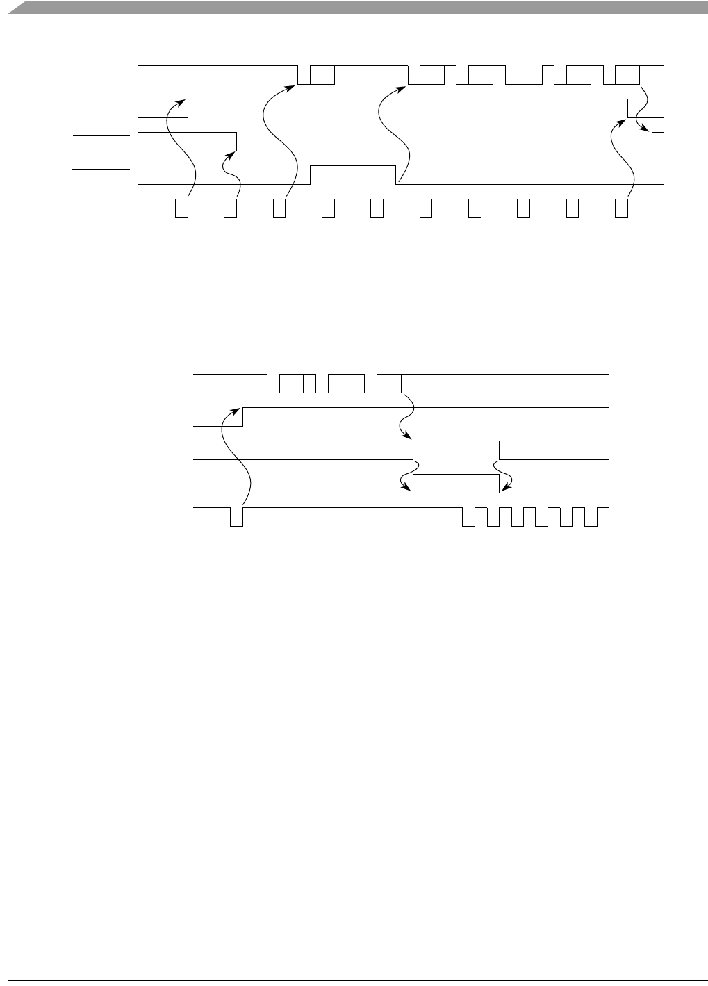
MCF548x Reference Manual, Rev. 3
26-36 Freescale Semiconductor
Figure 26-28. Modem Control and Transmitter
If PSCnRTS is programmed to be RxRTS, the PSCnRTS output is automatically asserted and negated by
the receiver. The PSCnRTS is asserted when the receiver is ready and the number in the RxFIFO is less
than the threshold, and PSCnRTS is negated when the receiver is disabled or the RxFIFO has more data
than the threshold.
Figure 26-29. Modem Control and Receiver
26.4.2 Multidrop Mode
The UART can be programmed to operate in a wakeup mode for multidrop or multiprocessor applications.
The mode is selected by setting bits 3 and 4 in mode register 1 (PSCMR1). This mode of operation allows
the master station to be connected to several slave stations (a maximum of 256). In this mode, the master
transmits an address character followed by a block of data characters targeted for one of the slave stations.
The slave stations have their channel receivers disabled. However, they continuously monitor the data
stream sent out by the master station. When an address character is sent by the master, the slave receiver
channel notifies its respective CPU by setting the RxRDY bit in the USR and generating an interrupt (if
programmed to do so). Each slave station CPU then compares the received address to its station address
and enables its receiver if it wishes to receive the subsequent data characters or block of data from the
master station. Slave stations not addressed continue to monitor the data stream for the next address
character. Data fields in the data stream are separated by an address character. After a slave receives a
block of data, the slave station's CPU disables the receiver and initiates the process again.
A transmitted character from the master station consists of a start bit, a programmed number of data bits,
an address/data (A/D) bit flag, and a programmed number of stop bits. The A/D bit identifies the type of
character being transmitted to the slave station. The character is interpreted as an address character if the
Module_En_B
Enable
TX Assert
RTS Write
C1 Write
C2 Write
C3 Start
Break Write
C4 End
Break Write
C5 Disable
TX
C1 C2 C3 C4 C5BreakPSCnTXD
Transmitter
PSCnRTS
Enabled
PSCnCTS
Command
from Bus
Module_En_B
Read
Status Read
Status Read
Status
C1 C2PSC_RXD
Receiver
FU
Enabled
PSC_RTS
Command
from Bus
C3
Read
Data Read
Data Read
Data
Enable
Receiver

Functional Description
MCF548x Reference Manual, Rev. 3
Freescale Semiconductor 26-37
A/D bit is set or as a data character if the A/D bit is cleared. The polarity of the A/D bit is selected by
programming bit 2 of PSCMR1. PSCMR1 should be programmed before enabling the transmitter and
loading the corresponding data bits into the transmit buffer.
In multidrop mode, the receiver continuously monitors the received data stream, regardless of whether it
is enabled or disabled. If the receiver is disabled, it sets the RxRDY bit and loads the character into the
receiver holding register FIFO stack provided the received A/D bit is a 1 (address tag). The character is
discarded if the received A/D bit is a 0 (data tag). If the receiver is enabled, all received characters are
transferred to the CPU via the receiver holding register stack during read operations.
In either case, the data bits are loaded into the data portion of the stack while the A/D bit is loaded into the
status portion of the stack normally used for a parity error (PSCSR bit 5). Framing error, overrun error, and
break detection operate normally. The A/D bit takes the place of the parity bit; therefore, parity is neither
calculated nor checked. Messages in this mode may still contain error detection and correction
information. One way to provide error detection, if 8-bit characters are not required, is to use software to
calculate parity and append it to the 5-, 6-, or 7-bit character.
26.4.3 Modem8 Mode
Figure 26-30 shows an example waveform in 8-bit modem mode.
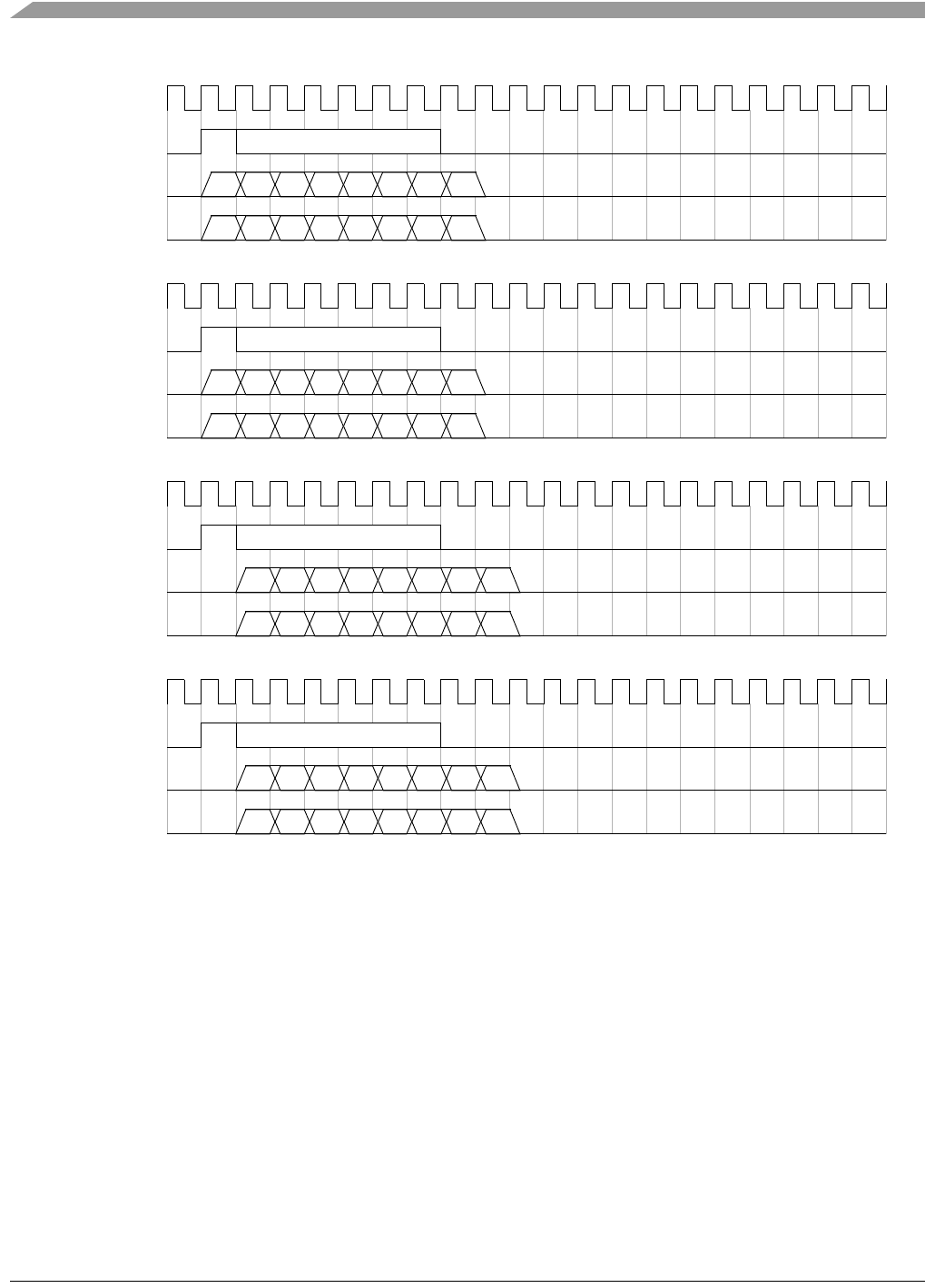
MCF548x Reference Manual, Rev. 3
26-38 Freescale Semiconductor
Figure 26-30. Waveform of Modem8 Mode
The transmitter starts to transmit the first bit at the rising edge of the PSCFSYNC or one clock after the
rising edge of the PSCFSYNC, according to the value in the DTS1 bit in the control register PSCSICR.
The SHDIR bit in the PSCSICR controls the order whether the LSB or the MSB is output first. The width
of the frame sync pulse makes no difference.
Similarly the receiver starts to receive a sample at the rising edge of the PSCFSYNC or one clock after the
rising edge.
The PSCFSYNC is sampled at the negative edge of the bit clock.
26.4.4 Modem16 Mode
Figure 26-31 shows an example of the waveform in 16-bit modem mode.
PSCBCLK
D7 D4 D3D6 D5 D2 D1 D0
PSCFSYNC
PSCnTXD
D7 D4 D3D6 D5 D2 D1 D0PSCnRXD
DTS1 = 0 & SHDIR = 0
PSCBCLK
D0 D3 D4D1 D2 D5 D6 D7
PSCFSYNC
PSCnTXD
D0 D3 D4D1 D2 D5 D6 D7PSCnRXD
DTS1 = 0 & SHDIR = 1
PSCBCLK
D7 D4 D3D6 D5 D2 D1 D0
PSCFSYNC
PSCnTXD
D7 D4 D3D6 D5 D2 D1 D0PSCnRXD
DTS1 = 1 & SHDIR = 0
PSCBCLK
D0 D3 D4D1 D2 D5 D6 D7
PSCFSYNC
PSCnTXD
D0 D3 D4D1 D2 D5 D6 D7PSCnRXD
DTS1 = 1 & SHDIR = 1

Functional Description
MCF548x Reference Manual, Rev. 3
Freescale Semiconductor 26-39
Figure 26-31. Waveform of Modem16 Mode
The function of this mode is the same as 8-bit modem mode except that the transmit/receive data length is
16 bit.
26.4.5 AC97 Mode
Figure 26-32 shows the waveform in AC97 modem mode.
Figure 26-32. Waveform of AC97 Mode
In AC97 mode, the PSCBCLK is the bit clock input and, different from 8/16 bit modem mode, the
PSCnRTS is the frame sync output. Figure 26-33 shows an example connection to a AC97 CODEC chip.
Figure 26-33. An Example Connection to AC97 CODEC
PSCBCLK
D15 D12 D11D14 D13 D10 D9
PSCFSYNC
PSCnTXD
PSCnRXD
D4 D3D6 D5 D2 D1 D0D8 D7
D15 D12 D11D14 D13 D10 D9 D4 D3D6 D5 D2 D1 D0D8 D7
PSCBCLK
D15 D1 D0D14 D19 D18
PSCnRTS
PSCnTXD
PSCnRXD
D19 D18D0 D1D1
D15 D1 D0D14 D19 D18 D19 D18D0 D1D1
81.4 ns (12.288 MHz)
20.8 µs (48.0 kHz)
D0
D0
D15
D15
D14
D14
Slot #0 (16-bit) Slot #1 (20-bit) Slot #12 (20-bit)
BITCLK
SYNC
XTL_IN
XTL_OUT
SDATA_IN
RESET
SDATA_OUT
AC97 CODEC
PSC_BIT_CLK
PSC_RTS
PSC_RXD
PSC_TXD
PSC

MCF548x Reference Manual, Rev. 3
26-40 Freescale Semiconductor
26.4.5.1 Transmitter
The transmitter starts to transmit the first bit at the one clock after the rising edge of the frame sync. The
first slot, slot #0, is 16 bits wide while the other slot, from slot #1 to slot #12, is 20 bits wide. Because the
transmit order is the MSB first, the SHDIR bit in the PSCSICR should be a value 0. The transmitter keeps
the output low until the receiver detects the ‘CODEC ready’ condition, which is indicated by a high in the
first bit of a new frame. Since receive data is sampled on the falling edge of the bit clock, the frame has
already started when a ‘CODEC ready’ condition is detected by the receiver. For this reason, when the
‘CODEC ready’ condition is detected, a transmission starts at the next frame (one clock after the next
frame sync). The transmitter stops transmission from the beginning of the frame in which the first bit of
the receiver frame was detected to be low, i.e. CODEC is not ready. During transmission, the transmitter
fills each of the 13 time slots of the AC97 frame with samples from the TxFIFO.
26.4.5.2 Receiver
The receiver starts to receive slot #0 data one bit clock after the rising edge of a frame sync. Until the
receiver detects a ‘CODEC ready’ condition, no data is put into the RxFIFO for that frame. When a
‘CODEC ready’ is detected, the receiver starts loading the RxFIFO with the received time slot samples
and continues to do so until a 0 is received in the first bit of a new frame.
26.4.5.3 Low Power Mode
PSC monitors the first three timeslots of each transmitter frame in order to detect the power down
condition for the AC97 digital interface. Detection of the power down condition is done as follows:
1. The first three bits of slot #0 must be 1 indicating that this transmitter frame is valid, and that slots
#1 and #2 are valid.
2. Slot #1 contains the address of the power down register (26 hex)
3. Slot #2 contains a 1 in the fourth bit (bit 12/PR4 in power down register)
Table 26-37. Slot Functions in AC97
Slot
Number
Output (PSCnTXD) Input (PSCnRXD)
Slot Name Bit Description Slot Name Bit Description
Slot #0 Tag 15 Frame valid Tag 15 CODEC ready
14 Control register address valid 14 Slot #1 data valid
13 Control register data valid 13 Slot #2 data valid
12 Left playback PCM data valid 12 Slot #3 data valid
11 Right playback PCM data valid 11 Slot #4 data valid
Slot #1 Control
address
19 Read/Write=1/0 Status
address
19 0
18:12 Control register number 18:12 Control register number
Slot #2 Control data 19:4 Write data.
0 in read
Status data 19:4 Control register read data
Slot #3 Left PCM
playback
19:0 PCM audio data left Left PCM
record
19:0 PCM record data left
Slot #4 Right PCM
playback
19:0 PCM audio data right Right PCM
record
19:0 PCM record data right
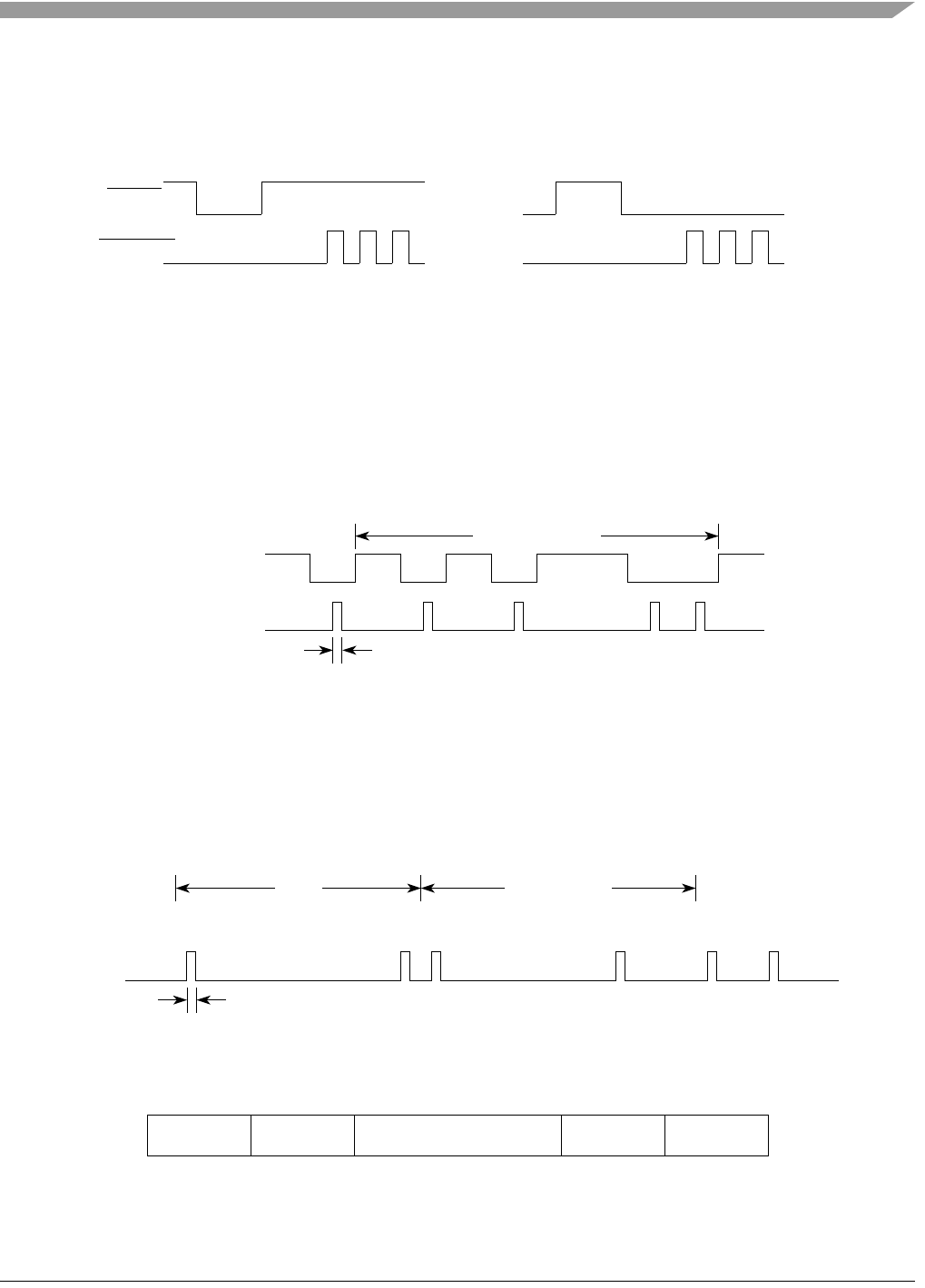
Functional Description
MCF548x Reference Manual, Rev. 3
Freescale Semiconductor 26-41
Leaving low power mode can be done via either a warm or cold reset (Figure 26-34). The CPU performs
a warm reset by writing a 1 to the AWR bit of SICR register for a minimum of 1 us. The AWR bit forces
a 1 on PSCnRTS, which is used as the frame sync output in AC97 mode. The pulse width of warm or cold
reset should be dependent on AC97 codec chip.
Figure 26-34. AC97 Cold and Warm Reset
26.4.6 SIR Mode
The data format in SIR mode is similar to that of UART mode. Each data consists of a start bit, 8 bit data,
and a stop bit. Each bit of data is encoded so that a 0 is encoded as 3/16 of the bit time pulse (or 1.6 υs
pulse), and a 1 is encoded as no pulse. Similarly, the received serial pulse is decoded as a 0, and an absence
of a pulse is decoded as a 1. Figure 26-35 is an example of data stream of UART and SIR.
Figure 26-35. Data Format in SIR Mode
26.4.7 MIR Mode
26.4.7.1 Data Format
The encoded pulse width of data in MIR mode is 1/4 of the bit duration and the transfer is synchronous.
Figure 26-36. Data Format in MIR Mode
The packet format is similar to HDLC packet format
Figure 26-37. MIR Packet Format
Cold reset Warm reset
RESET
PSCBCLK
PSCFSYNC
PSCBCLK
UART Data Format
3/16 of the bit width or 1.6 µs
010101 1100
SIR Data Format
Data Bits (8-bit)START Bit STOP Bit
Binary Data
1/4 of the bit width
011111 1100 111101 0101 1
Flag Character FE
STA STA FCS STODATA
01111110 01111110 16-bit CRC 01111110
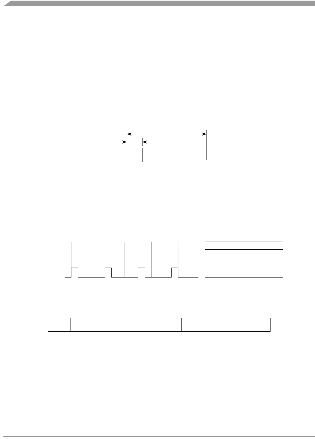
MCF548x Reference Manual, Rev. 3
26-42 Freescale Semiconductor
The STA represents the start of the frame and the STO represents the end of the frame. Both of STA and
STO are defined as 01111110 in binary format. In the transmitted data and FCS, a 0 is inserted after 5
consecutive 1s. The FCS is a 16-bit CRC defined as:
Eqn. 26-3
26.4.7.2 Serial Interaction Pulse (SIP)
The MIR and FIR system must emit SIP at least once per 500ms while the connection lasts, in order to
inform slower systems (SIR) not to interfere with the link. If the SIPEN bit in IRCR1 is high, the
transmitter automatically appends one SIP after every frame. SIP also can be sent by writing 1 to SIPREQ
bit in IRCR2. If SIPREQ is high and the transmitter is in an idle state, one SIP is sent and the SIPREQ bit
is automatically cleared. Figure 26-38 illustrates how SIP is defined.
Figure 26-38. Serial Interaction Pulse (SIP)
26.4.8 FIR Mode
26.4.8.1 Data Format
The data field is 4 PPM encoded by the transmitter. Data encoding is done LSB first. Each chip duration
is 125 ns.
Figure 26-39. Data Format in FIR Mode
Figure 26-40 shows the packet format.
The preamble (PA) field is used by a receiver to establish phase lock. After receiving the start flag (STA),
the receiver begins to interpret the 4 PPM encoded symbols. The receiver continues receiving until it
receives the stop flag (STO). The FCS is a 32-bit CRC defined as:
Eqn. 26-4
The chip patterns for PA, STA, and STO are defined in Table 26-38.
Figure 26-40. FIR Mode Packet Format
PA STA DATA FCS STO
CRC x() x16 x12 x51+++=
1.6 µs
8.7 µs
Binary Data 00011011
Bit Pair 4 PPM Data
00 1000
01 0100
10 0010
11 0001
CRC x() x32 x26 x23 x22 x16 x12 x11 x10
+++++++ x8x7x5x4
++++ x
2x1+++=

Functional Description
MCF548x Reference Manual, Rev. 3
Freescale Semiconductor 26-43
.
26.4.9 PSC FIFO System
The receive FIFO stack consists of the FIFO and a receiver shift register connected to the RxD. Data is
assembled in the receiver shift register and loaded into the FIFO at the location pointed to by the FIFO
write pointer.
Reading the Rx buffer produces an output of data from the location pointed to by the FIFO read pointer.
After the read cycle, data at the top of the FIFO stack is popped and the Rx shift register can add new data
at the bottom of the FIFO. The standard FIFO controller used in MCF548x peripherals, such as the PSCs,
was designed to control either a transmit (Tx) or a receive (Rx) FIFO
Depending on whether the FIFO is set for Tx or Rx, alarm and granularity are measured differently, either:
• valid data bytes (Tx FIFO)
• empty bytes (Rx FIFO)
For both Tx and Rx FIFOs:
• Alarm specifies a threshold at which the FIFO generates an interrupt to either:
— Multichannel DMA
— CPU (alternate)
• Granularity specifies a threshold at which the interrupt goes away.
Each PSC provides two control lines to the Multichannel DMA system, control the transfer from and to
the PSC FIFO. The FIFOs can be accessed as follows:
• 8-bit codec mode or UART mode
— Can access FIFOs either 1, 2, or 4 one-byte samples at a time.
• 16-bit codec mode:
— Can access FIFOs 1 or 2 two-byte samples at a time.
• 32-bit and 32-bit codec mode
— Can access FIFOs four-byte samples at a time
• AC97 mode:
— Must access FIFOs one sample at a time
— In addition, when the Rx FIFO is being read, a “1” in bit 20 (21st bit of the sample) marks this
sample as the first time slot of a new frame.
Block error mode is always selected because PSCMR1n[ERR] is hard-wired high. In block mode PSCSRn
shows a logical OR of all characters received after the last RESET ERROR STATUS command. Block mode
offers a data-reception speed advantage where the software overhead of error-checking each character
cannot be tolerated. Errors are not detected until the check is done at the end of an entire message; the
faulting character is not identified.
Reading PSCSRn does not affect the FIFO. The FIFO is popped only when the Rx buffer is read. If the Rx
FIFO is completely full, a new character is held in the Rx shift register until space is available. However,
if a second new character is received, contents of the character in the Rx shift register is lost. The FIFOs
Table 26-38. Chip Patterns for FIR Fields
PA 1000 0000 1010 1000 (16 times repeated)
STA 0000 1100 0000 1100 0110 0000 0110 0000
STO 0000 1100 0000 1100 0000 0110 0000 0110
first chip last chip
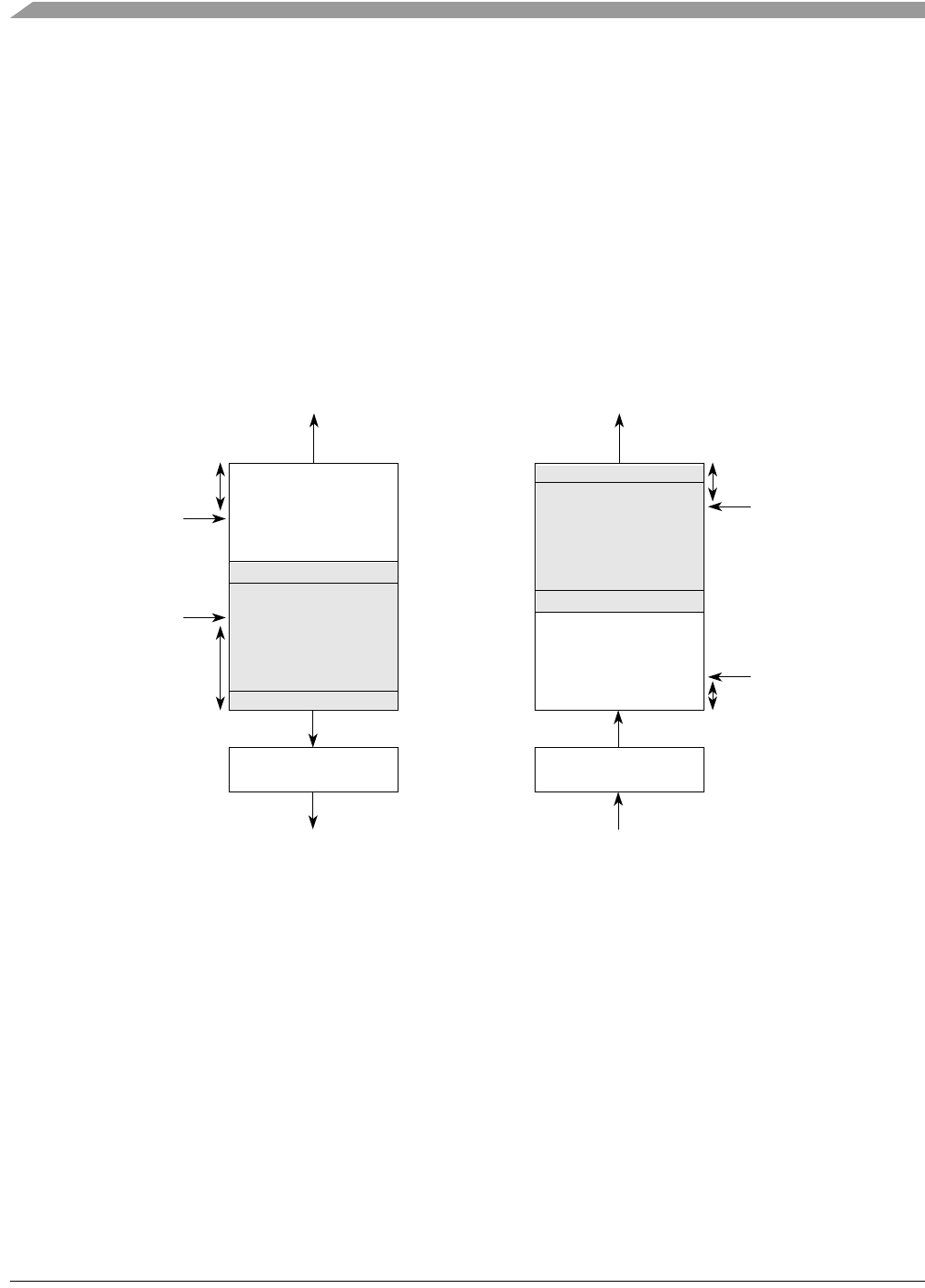
MCF548x Reference Manual, Rev. 3
26-44 Freescale Semiconductor
are unaffected, and PSCSRn[ERR] sets when the receiver detects the start bit of the new overrunning
character.
To support flow control, the receiver can be programmed to automatically negate and assert RTS. In which
case, the receiver automatically negates RTS when a valid start bit is detected and the FIFO stack is full.
The receiver asserts RTS when a FIFO position becomes available.
Overrun errors can be prevented by connecting RTS to the CTS input of the transmitting device.
NOTE
The receiver can still read characters in the FIFO stack if the receiver is
disabled. If the receiver is reset, the FIFO stack, RTS control, all receiver
status bits, and interrupt requests are reset. No more characters are received
until the receiver is re-enabled.
Figure 26-41. PSC FIFO System
26.4.9.1 RX FIFO
The RX FIFO space is 512 bytes. For an Rx FIFO, the alarm value is not the amount of data in the Rx
FIFO. Instead, an interrupt occurs as a result of the amount of empty space remaining in the Rx FIFO.
These facts are described in Figure 26-41.
If it is known how much data is needed in the Rx FIFO to cause an interrupt, the value that must be written
into the alarm register is the FIFO size minus the number of data bytes in the FIFO
Unlike the alarm value, granularity value represents a number of data bytes, not empty space.
empty
FIFO space
last byte to send
first byte to send
Granularity
Level
(value multplied by 4)
(example: 0x005)
Address:
0x1FF
Alarm Level
“almost empty”
(example: 0x010)
0x0
0x0
0x1FF
Transmitter
Tx Line
empty
FIFO space
last received byte
first received byte
Receiver
Rx Line
Granularity
Level
(value multplied by 4)
(example: 0x004)
Alarm Level
“almost full”
(example: 0x008)
Internal Bus Interface

Functional Description
MCF548x Reference Manual, Rev. 3
Freescale Semiconductor 26-45
NOTE
In AC97, the number of data bytes are four times the number of time slot
samples in the FIFO. Because, each 20-bit sample uses an entire 32-bit
longword in the FIFO.
For the Rx FIFO, the value can be between 0 and 7 bytes only. Therefore, the interrupt has hysteresis. For
example, the interrupt goes active when the Rx FIFO is “almost full” (i.e., the amount of empty space is
less than the alarm level). It stays active until enough data is read out of the Rx FIFO so that the amount
of data left in the FIFO is less than the granularity level.
For the example (see Figure 26-41) this means:
The requestor to the Multichannel DMA to emptying the RX FIFO becomes active if the empty
space in the FIFO is less than 8 bytes (504 data bytes are in the FIFO).
The requester became inactive if 4 bytes are left in the FIFO. (508 byte space now)
When the Multichannel DMA is servicing the FIFOs, this process works well. However, if the CPU is
servicing the FIFOs, the interrupt has no hysteresis.
For example, the alarm level is used for both activating and deactivating the CPU interrupt.
When using the Multichannel DMA you must specify a non-zero granularity to get FIFO underrun errors.
This is due to its internal pipelining.
Multichannel DMA does not immediately stop accessing the FIFO when the FIFO interrupt goes away.
26.4.9.2 TX FIFO
The TX FIFO space is 512 bytes. For a Tx FIFO, the alarm value specifies a threshold in terms of DATA
bytes, not in terms of empty space as with the Rx FIFO. Once the amount of data in the Tx FIFO falls
below the alarm level, an interrupt activates. The interrupt indicates the Tx FIFO is” almost empty” and
needs more data. Tx FIFO granularity is specified in terms of empty bytes, not the number of data bytes
as with the Rx FIFO. For more informations see also Figure 26-41. The granularity value range is 0–7.
The Tx FIFO controller hardware multiplies this value by 4, to establish the actual level at which the FIFO
alarm goes away. For the Tx FIFO, the alarm goes away when the number of empty bytes left in the Tx
FIFO is less than or equal to:
• 0 (Granularity value 0)
• 4 (Granularity value 1)
• 8 (Granularity value 2)
• 12 (Granularity value 3)
• 16 (Granularity value 4)
• 20 (Granularity value 5)
• 24 (Granularity value 6)
• 28 (Granularity value 7)
The FIFO interrupt stays active until Multichannel DMA writes enough data into the Tx FIFO to reach the
granularity level. Once the granularity level is reached, the interrupt goes away.
For the example (see Figure 26-41) it means:
The requestor to the Multichannel DMA to filling the TX FIFO becomes active if the amount of
data in the FIFO is less then 16 data.
The requester became inactive if less than 20 (5 ×4) bytes space in the FIFO.
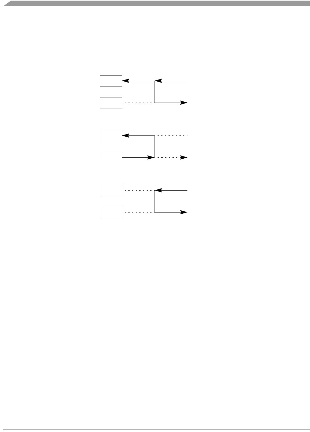
MCF548x Reference Manual, Rev. 3
26-46 Freescale Semiconductor
26.4.10 Looping Modes
The UART can be configured to operate in various looping modes as shown in Figure 26-42. These modes
are useful for local and remote system diagnostic functions, and can be used in modem mode and IrDA
mode as well as UART mode. The modes are described in the following paragraphs.
Figure 26-42. Looping Modes Functional Diagram
The UART's transmitter and receiver should both be disabled when switching between modes. The
selected mode is activated immediately upon mode selection, regardless of whether a character is being
received or transmitted.
26.4.10.1 Automatic Echo Mode
In the automatic echo mode, the UART automatically retransmits the received data on a bit-by-bit basis.
The local CPU-to-receiver communication continues normally, but the CPU-to-transmitter link is
disabled. While in this mode, received data is clocked on the receiver clock and retransmitted on TxD. The
receiver must be enabled, but the transmitter need not be enabled.
Because the transmitter is not active, the TxEMP and TxRDY bits in USR are inactive, and data is
transmitted as it is received. Received parity is checked, but not recalculated for transmission. Character
framing is also checked, but stop bits are transmitted as received. A received break is echoed as received
until the next valid start bit is detected.
26.4.10.2 Local Loopback Mode
TxD is internally connected to RxD in the local loopback mode. This is useful for testing the operation of
a local UART module channel by sending data to the transmitter and checking data assembled by the
receiver. In this manner, correct channel operations can be assured. Also, both transmitter and
CPU-to-receiver communications continue normally in this mode. While in this mode, the RxD input data
RX
TX disabled
PSCnRXD
PSCnTXD
Automatic echo
RX
TX
disabled PSCnRXD
PSCnTXD
Local loop back
RX
TX disabled
PSCnRXD
PSCnTXD
Remote loop back
disabled

Resets
MCF548x Reference Manual, Rev. 3
Freescale Semiconductor 26-47
is ignored, the TxD is held marking, and the receiver is clocked by the transmitter clock. The transmitter
must be enabled, but the receiver need not be enabled.
26.4.10.3 Remote Loopback Mode
In this mode, the channel automatically transmits received data on the TxD output on a bit-by-bit basis.
The local CPU-to-transmitter link is disabled. This mode is useful in testing receiver and transmitter
operation of a remote channel. While in this mode, the receiver clock is used for the transmitter.
Because the receiver is not active, received data cannot be read by the CPU, and the error status conditions
are inactive. Received parity is not checked and is not recalculated for transmission. Stop bits are
transmitted as received. A received break is echoed as received until the next valid start bit is detected.
26.5 Resets
26.5.1 General
This section describes how to reset the device. CR refers to PSCCR.
26.5.2 Description of Reset Operation
26.5.2.1 Reset
When there is a reset, the PSC module goes to its initial state.
26.5.2.2 CRSRX
Writing the RESET RECEIVER command to the command control register PSCCR resets the receiver.
26.5.2.3 CRSTX
Writing the RESET TRANSMITTER command to the command control register PSCCR resets the
transmitter.
26.5.2.4 CRSES
Writing the RESET ERROR STATUS command to the command control register PSCCR resets the error
status held in the status register PSCSR.
Table 26-39. Reset Summary
Reset Priority Source Characteristics
Reset High Input port Hardware reset
CRSRX Low Command to PSCCR Reset receiver
CRSTX Low Command to PSCCR Reset transmitter
CRSES Low Command to PSCCR Reset error status

MCF548x Reference Manual, Rev. 3
26-48 Freescale Semiconductor
26.6 Interrupts
This section describes interrupts originated by this module.
26.6.1 Description of Interrupt Operation
26.6.1.1 Processor Interrupt
This is the interrupt to the processor. There are five conditions to assert this interrupt:
• The IPC interrupt condition is met if the modem control input port (PSCnCTS) is changed and lasts
for a certain time.This interrupt is usually used in UART mode though it works under all modes.
• The DB condition is met if the PSCnRXD is held low for more than a character duration in UART
and SIR mode.
• The RxRDY is from PSCISR[9]. It is asserted when the alarm of the RXFIFO is asserted
(PSCIMR1[6] = 1) or there is at least one data in RXFIFO (PSCMR1[6] = 0).
• The TxRDY is different from cb_req_tx. It is asserted when
— the transmitter is enabled
— the number of the TXFIFO is less than or equal to the threshold TFAR
— the corresponding PSCIMR bit, PSCIMR[TxRDY(=8)], is high and enabled, i.e. when
PSCISR[8] (=SR[10]=(count<=alarm)) & PSCIMR[8] & ENTX
• The DEOF is from PSCISR[7]. It is asserted when there is an EOF in the RXFIFO.
26.7 Software Environment
26.7.1 General
This section provides information pertinent to programming the device.
Table 26-40. Interrupt Summary
Interrupt Mode Source Description
Processor
Interrupt
UART IPC The state of the modem control input ports had changed and a
certain time has passed.
DB Detected delta break. The input port RXD has kept low for a
certain time.
RXRDY There is one or more data in the RxFIFO
FU The number in the RxFIFO is more than the threshold
TXRDY The number in the TxFIFO is less than the threshold
modem
IrDA
RXRDY There is one or more data in the RxFIFO
FU The number in the RxFIFO is more than the threshold
TXRDY The number in the TxFIFO is less than the threshold

Software Environment
MCF548x Reference Manual, Rev. 3
Freescale Semiconductor 26-49
26.7.2 Configuration
26.7.2.1 UART Mode
The following is a sample initialization sequence for UART mode.
Table 26-41. Sample Initialization Sequence for UART Mode
Step
No. Register Value Details Meaning
1 PSCSICR 08 RxDCD=1 DCD input effects receiver
SIM[2:0]=000 UART mode
2 PSCCSR DD RCS[3:0]=1101 Receiver baud rate is made from PSC timer
TCS[3:0]=1101 Transmitter baud rate is made from PSC timer
3 PSCCTUR 00 CT[15:0]=108 (dec) Divide sys_clk by 108. If f(sys_clk) = 33.3333 MHz,
baud rate is 9600 bps.
PSCCTLR 6C
4 PSCCR 20 MISC=010 Reset receiver and RxFIFO
30 MISC=011 Reset transmitter and TxFIFO
40 MISC=100 Reset all error status
50 MISC=101 Reset break change interrupt
10 MISC=001 Reset MR pointer
5 PSCIMR 8700 IPC=1 Enable input port change interrupt
DB=1 Enable delta break interrupt
RxRDY or FU=1 Enable receiver interrupt/request
TxRDY=1 Enable transmitter interrupt/request
6 PSCACR 03 IEC1=1 Enable state change of DCD
IEC0=1 Enable state change of PSCnCTS
7 PSCMR1 23 RxRTS=0 Receiver has no effect on PSCnRTS
RxIRQ=0 RX interrupt is from RxRDY (one byte)
ERR=1 (fixed) Block error mode
PM[1:0]=00, PMT=0 even parity
BC[1:0]=11 8 bit
8 PSCMR2 37 CM[1:0]=00 Normal mode (not test mode)
TxRTS=1 PSCnRTS is controlled by transmitter
TxCTS=1 PSCnCTS controls transmitter
SB[3:0]=0111 1 stop bit

MCF548x Reference Manual, Rev. 3
26-50 Freescale Semiconductor
26.7.2.2 Modem8 Mode
Applying the clock to the PSCBCLK input and programming the control registers are required to initialize
in modem8 mode. The following table describes a sample initialization sequence.
9 PSCRFCR 0F WRITE TAG = 00 Not EOF
FRMEN=1 Enable frame mode
GR[2:0]=100 Granularity is 4 byte
10 PSCTFCR 0F WRITE TAG = 00 Not EOF
FRMEN=1 Enable frame mode
GR[2:0]=100 Granularity is 16 byte
11 PSCRFAR 00F0 ALARM[8:0]=0F0 Request is asserted if # of data >= 240
12 PSCTFAR 00F0 ALARM[8:0]=0F0 Request is asserted if # of empty >= 240
13 PSCOPSET 01 RES=0 Bit is always 0.
RTS=1 Assert RTS (PSCnRTS=0)
14 PSCCR 05 TC=01 Enable transmitter
RC=01 Enable receiver
Table 26-42. Sample Initialization Sequence for Modem8 Mode
Step
No. Register Value Details Meaning
1 PSCSICR 01 DTS1=0 The 1st bit is in the rising edge of sync
SHDIR=0 MSB first
SIM[2:0]=001 modem8 mode
2 PSCCR 20 MISC=010 Reset receiver and RxFIFO
30 MISC=011 Reset transmitter and TxFIFO
40 MISC=100 Reset all error status
3 PSCIMR 0300 IPC=0 Disable input port change interrupt
RxRDY or FU=1 Enable receiver interrupt/request
TxRDY=1 Enable transmitter interrupt/request
4 PSCRFCR 0F WRITE TAG=00 Not EOF
FRMEN=1 Enable frame mode
GR[2:0]=100 Granularity is 4 byte
Table 26-41. Sample Initialization Sequence for UART Mode (Continued)
Step
No. Register Value Details Meaning

Software Environment
MCF548x Reference Manual, Rev. 3
Freescale Semiconductor 26-51
26.7.2.3 Modem16 Mode
The configuration sequence in modem16 mode is almost the same as in modem8 mode except that the first
write value to the SIM[2:0] in PSCSICR should be 3’b010.
26.7.2.4 AC97 Mode
Applying a 12.288 MHz clock to the PSCBCLK input and programming the control registers are required
to initialize in AC97 mode. The following table describes a sample sequence.
5 PSCTFCR 0F WRITE TAG=00 Not EOF
FRMEN=1 Enable frame mode
GR[2:0]=100 Granularity is 16 byte
6 PSCRFAR 00F0 ALARM[8:0]=0F0 Request is asserted if # of data >= 240
7 PSCTFAR 00F0 ALARM[8:0]=0F0 Request is asserted if # of empty >= 240
8 PSCCR 05 TC=01 Enable transmitter
RC=01 Enable receiver
Table 26-43. A Sample Initialization Sequence for AC97 Mode
Step
No. Register Value Details Meaning
1 PSCSICR 03 ACRB=1 Not cold reset
AWR=0 Not warm reset
SIM[2:0]=011 AC97 mode
2 PSCCR 20 MISC=010 Reset receiver and RxFIFO
30 MISC=011 Reset transmitter and TxFIFO
40 MISC=100 Reset all error status
3 PSCIMR 0300 IPC=0 Disable input port change interrupt
RxRDY or FU=1 Enable receiver interrupt/request
TxRDY=1 Enable transmitter interrupt/request
4 PSCRFCR 0F WRITE TAG = 00 Not EOF
FRMEN=1 Enable frame mode
GR[2:0]=100 Granularity is 4 byte
5 PSCTFCR 0F WRITE TAG = 00 Not EOF
FRMEN=1 Enable frame mode
GR[2:0]=100 Granularity is 16 byte
Table 26-42. Sample Initialization Sequence for Modem8 Mode (Continued)
Step
No. Register Value Details Meaning

MCF548x Reference Manual, Rev. 3
26-52 Freescale Semiconductor
26.7.2.5 SIR Mode
Here is a sample configuration sequence in SIR mode.
6 PSCRFAR 00F0 ALARM[8:0]=0F0 Request is asserted if # of data >= 240
7 PSCTFAR 00F0 ALARM[8:0]=0F0 Request is asserted if # of empty >= 240
8 PSCCR 05 TC=01 Enable transmitter
RC=01 Enable receiver
Table 26-44. A Sample Initialization Sequence for SIR Mode
Step
No. Register Value Details Meaning
1 PSCSICR 04 SIM[2:0]=100 SIR mode
2 PSCCSR DD RCS[3:0]=1101 Receiver baud rate is made from PSC timer
TCS[3:0]=1101 Transmitter baud rate is made from PSC timer
3 PSCCTUR 00 CT[15:0]=108 (dec) Divide sys_clk by 108. If f(sys_clk) = 33.3333 MHz,
baud rate is 9600 bps.
PSCCTLR 6C
4 PSCCR 20 MISC=010 Reset receiver and RxFIFO
30 MISC=011 Reset transmitter and TxFIFO
40 MISC=100 Reset all error status
10 MISC=001 Reset MR pointer
5 PSCIMR 0300 IPC=0 Disable input port change interrupt
DB=0 Disable delta break interrupt
RxRDY or FU=1 Enable receiver interrupt/request
TxRDY=1 Enable transmitter interrupt/request
6 PSCACR 00 IEC1=0 Disable state change of DCD
IEC0=0 Disable state change of PSCnCTS
7 PSCMR1 33 RxRTS=0 Receiver has no effect on PSCnRTS
RxIRQ=0 Receiver interrupt is from RxRDY (one byte)
ERR=1 (fixed) Block error mode
PM[1:0]=10, PMT=0 No parity
BC[1:0]=11 8 bit
Table 26-43. A Sample Initialization Sequence for AC97 Mode (Continued)
Step
No. Register Value Details Meaning

Software Environment
MCF548x Reference Manual, Rev. 3
Freescale Semiconductor 26-53
26.7.2.6 MIR Mode
Applying clock to the PSCBCLK input and programming the control registers are required to initialize in
MIR mode. Here is a sample sequence when the input frequency of PSCBCLK is 18.432 MHz. (1.152
MHz x 16).
8 PSCMR2 07 CM[1:0]=00 Normal mode (not test mode)
TxRTS=0 PSCnRTS is not controlled by transmitter
TxCTS=0 PSCnCTS does not control transmitter
SB[3:0]=0111 1 stop bit
9 PSCIRCR1 00 FD=0 Receiver is disabled while transmitting
SPUL=1 Pulse width is 1.6 us
10 PSCIRSTR 36 IRSTIM=54 (dec) Counter value for 1.6 us pulse
11 PSCRFCR 0F WRITE TAG = 00 Not EOF
FRMEN=1 Enable frame mode
GR[2:0]=100 Granularity is 4 byte
12 PSCTFCR 0F WRITE TAG = 00 Not EOF
FRMEN=1 Enable frame mode
GR[2:0]=100 Granularity is 16 byte
13 PSCRFAR 00F0 ALARM[8:0]=0F0 Request is asserted if # of data >= 240
14 PSCTFAR 00F0 ALARM[8:0]=0F0 Request is asserted if # of empty >= 240
15 PSCCR 04 TC=01 Enable transmitter
RC=00 Receiver remains at disabled state.
Table 26-45. A Sample Initialization Sequence for MIR Mode
Step
No. Register Value Details Meaning
1 PSCSICR 05 SIM[2:0]=101 MIR mode
2 PSCIRMFD 0F FREQL=0 1.152 Mbps mode
M_FDIV[4:0]=01111 Frequency divide ratio is 16.
So f(PSCBCLK) should be 18.432 MHz.
3 PSCCR 20 MISC=010 Reset receiver and RxFIFO
30 MISC=011 Reset transmitter and TxFIFO
40 MISC=100 Reset all error status
10 MISC=001 Reset MR pointer
Table 26-44. A Sample Initialization Sequence for SIR Mode (Continued)
Step
No. Register Value Details Meaning

MCF548x Reference Manual, Rev. 3
26-54 Freescale Semiconductor
26.7.2.7 FIR Mode
Applying the clock to the PSCBCLK input and programming the control registers are required to initialize
in FIR mode. Here is a sample sequence when the input frequency of PSCBCLK is 64 MHz. Steps 3 to 11
are the same as in MIR mode.
4 PSCMR1 73 RxIRQ=1 receiver interrupt is from FU (over threshold)
5 PSCIMR 0380 IPC=0 Disable input port change interrupt
RxRDY or FU=1 Enable receiver interrupt/request
TxRDY=1 Enable transmitter interrupt/request
DEOF=1 Enable DEOF interrupt/request
6 PSCIRCR1 02 FD=0 Receiver is disabled while transmitting
SIPEN=1 Send SIP after every frame
7 PSCIRCR2 00 SIPREQ=0 SIP is not requested to send now
ABORT=0 Not send abort sequence now
NXTEOF=0 Next write is not EOF
8 PSCRFCR 0F WRITE TAG = 00 Not EOF
FRMEN=1 Enable frame mode
GR[2:0]=100 Granularity is 4 byte
9 PSCTFCR 0F WRITE TAG = 00 Not EOF
FRMEN=1 Enable frame mode
GR[2:0]=100 Granularity is 16 byte
10 PSCRFAR 00F0 ALARM[8:0]=0F0 Request is asserted if # of data >= 240
11 PSCTFAR 00F0 ALARM[8:0]=0F0 Request is asserted if # of empty >= 240
12 PSCCR 04 TC=01 Enable transmitter
RC=00 receiver remains at disabled state.
Table 26-46. A Sample Initialization Sequence for FIR Mode
Step
No. Register Value Details Meaning
1 PSCSICR 06 SIM[2:0]=110 FIR mode
2 PSCIRFFD 0F F_FDIV[3:0]=0111 Frequency divide ratio is 8.
So f(PSCBCLK) should be 64 MHz.
Table 26-45. A Sample Initialization Sequence for MIR Mode (Continued)
Step
No. Register Value Details Meaning

Software Environment
MCF548x Reference Manual, Rev. 3
Freescale Semiconductor 26-55
26.7.3 Programming
In any mode, after the configuration sequence, enabling the transmitter and writing data to the transmit
buffer sends serial data via the PSCnTXD port. Enabling the receiver makes the receiver ready and if there
is incoming data to PSCnRXD, the receiver decodes the input and stores the data in the FIFO.
26.7.3.1 MIR Mode
After initialization, writing data to the transmit buffer and enabling the transmitter sends data via the
PSCnTXD port. The STA, CRC (option), and STO are automatically added.
3 PSCCR 20 MISC=010 Reset receiver and RxFIFO
30 MISC=011 Reset transmitter and TxFIFO
40 MISC=100 Reset all error status
10 MISC=001 Reset MR pointer
4 PSCMR1 73 RxIRQ=1 Receiver interrupt is from FU (over threshold)
5 PSCIMR 0380 IPC=0 Disable input port change interrupt
RxRDY or FU=1 Enable receiver interrupt/request
TxRDY=1 Enable transmitter interrupt/request
DEOF=1 Enable DEOF interrupt/request
6 PSCIRCR1 02 FD=0 receiver is disabled while transmitting
SIPEN=1 Send SIP after every frame
7 PSCIRCR2 00 SIPREQ=0 SIP is not requested to send now
ABORT=0 Not send abort sequence now
NXTEOF=0 Next write is not EOF
8 PSCRFCR 0F WRITE TAG = 00 Not EOF
FRMEN=1 Enable frame mode
GR[2:0]=100 Granularity is 4 byte
9 PSCTFCR 0F WRITE TAG = 00 Not EOF
FRMEN=1 Enable frame mode
GR[2:0]=100 Granularity is 16 byte
10 PSCRFAR 00F0 ALARM[8:0]=0F0 Request is asserted if # of data >= 240
11 PSCTFAR 00F0 ALARM[8:0]=0F0 Request is asserted if # of empty >= 240
12 PSCCR 04 TC=01 Enable transmitter
RC=00 Receiver remains at disabled state.
Table 26-46. A Sample Initialization Sequence for FIR Mode (Continued)
Step
No. Register Value Details Meaning

MCF548x Reference Manual, Rev. 3
26-56 Freescale Semiconductor
After initialization and after enabling the receiver, the receiver is ready to receive data. While receiving
serial data, the receiver will eliminate STA and STO, and these flags are not written into the FIFO. After
receiving enough data, PSC asserts request/interrupt to prompt the processor to read the received data.
26.7.3.2 FIR Mode
After initialization, writing data to the TB and enabling the transmitter sends data via the PSCnTXD port.
The PA, STA, CRC (option), and STO are automatically added.
After initialization and after enabling the receiver, the receiver is ready to receive data. While receiving
serial data, the receiver will eliminate PA, STA, and STO, and these flags are not written into the FIFO.
After receiving enough data, PSC asserts request/interrupt to prompt the processor to read the received
data.

MCF548x Reference Manual, Rev. 3
Freescale Semiconductor 27-1
Chapter 27
DMA Serial Peripheral Interface (DSPI)
This chapter describes the use of the DMA serial peripheral interface (DSPI) implemented on the
MCF548x processor.
27.1 Overview
The DMA serial peripheral interface (DSPI) block provides a synchronous serial bus for communication
between an MCU and an external peripheral device. The DSPI supports up to eight queued SPI transfers
(four receive and four transmit) in the DSPI resident FIFOs eliminating CPU intervention between
transfers.
For queued operations, the SPI queues reside in system RAM that is external to the DSPI. Data transfers
between the queues and the DSPI FIFOs are accomplished through the use of a DMA controller or through
host software.
27.2 Features
The MCF548x DSPI supports these SPI features:
• Full-duplex, three-wire synchronous transfers
• Master and slave modes
• Buffered transmit operation using the Tx FIFO with depth of up to 4 entries
• Buffered receive operation using the Rx FIFO with depth of up to 4 entries
• Tx and Rx FIFOs can be disabled individually for low-latency updates to SPI queues
• Visibility into Tx and Rx FIFOs for ease of debugging
• Programmable transfer attributes on a per-frame basis:
— Eight transfer attribute registers
— Serial clock with programmable polarity and phase
— Various programmable delays
— Programmable serial frame size of 4 to 16 bits, expandable with software control
— Continuously held chip select capability
• Four peripheral chip selects, expandable to 15 with external demultiplexer
• Deglitching support for up to seven peripheral chip selects with external demultiplexer
• DMA support for adding entries to Tx FIFO and removing entries from Rx FIFO:
— Tx FIFO is not full (TFFF)
— Rx FIFO is not empty (RFDF)
• Six interrupt conditions:
— End of queue reached (EOQF)
— Tx FIFO is not full (TFFF)
— Transfer of current frame complete (TCF)
— Attempt to transmit with an empty Tx FIFO (TFUF)
— Rx FIFO is not empty (RFDF)
— Frame received while Rx FIFO is full (RFOF)
• Modified SPI transfer formats for communication with slower peripheral devices
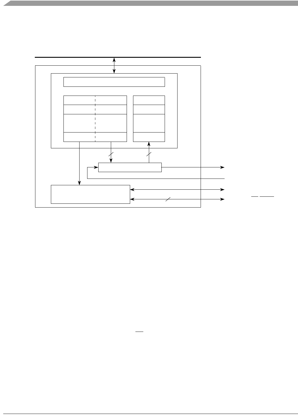
MCF548x Reference Manual, Rev. 3
27-2 Freescale Semiconductor
27.3 Block Diagram
Figure 27-1 shows a DSPI with external queues in system RAM.
Figure 27-1. DSPI with Queues and DMA
27.4 Modes of Operation
The DSPI has two modes of operation: master and slave. The two modes are entered by host software
writing to a register.
27.4.1 Master Mode
Master mode allows the DSPI to initiate and control serial communication. In this mode, the DSPISCK
signal and the DSPICSn signals are controlled by the DSPI and configured as outputs.
27.4.2 Slave Mode
The slave mode allows the DSPI to communicate with SPI bus masters. In this mode the DSPI responds
to externally controlled serial transfers. The DSPI cannot control serial transfers in slave mode. In slave
mode, the DSPISCK signal and the DSPICS0/SS signal are configured as inputs and provided by a bus
master.
DMA & Interrupt Control
TX FIFO
CMD Data Data
RX FIFO
Shift Register
SPI Baud Rate, Delay
and Transfer Control
16
DSPISOUT
DSPISIN
DSPISCK
DSPICSn/SS/PCSS
16
4
CommBus
DSPI

Signal Description
MCF548x Reference Manual, Rev. 3
Freescale Semiconductor 27-3
27.5 Signal Description
27.5.1 Overview
Table 27-1 lists the DSPI signals.
27.5.2 Detailed Signal Descriptions
27.5.2.1 DSPI Peripheral Chip Select/Slave Select (DSPICS0/SS)
In master mode, the DSPICS0 signal is a peripheral chip select output that selects which slave device the
current transmission is intended for.
In slave mode, the SS signal is a slave select input signal that allows an SPI master to select the DSPI as
the target for transmission.
27.5.2.2 DSPI Peripheral Chip Selects 2–3 (DSPICS[2:3])
DSPICS[2:3] are peripheral chip select output signals in master mode. In slave mode these signals are not
used.
27.5.2.3 DSPI Peripheral Chip Select 5/Peripheral Chip Select Strobe
(DSPICS5/PCSS)
When the DSPI is in master mode and the DMCR[PCSSE] bit is cleared, DSPICS5 is used to select the
slave device for which the current transfer is intended DSPICS5 is a peripheral chip select output signal.
PCSS provides a strobe signal that can be used with an external demultiplexer for deglitching of the n
signals. When the DSPI is in master mode and DMCR[PCSSE] is set, the PCSS provides the appropriate
timing for the decoding of the DSPICS[0,2,3] signals that prevents glitches from occurring.
This signal is not used in slave mode.
Table 27-1. Signal Properties
Name Input/Output
Function
Master Mode Slave Mode
DSPICS0/SS Input/Output Peripheral Chip Select 0 (output) Slave Select (input)
DSPICS[2:3] Output Peripheral Chip Select 2 - 3 Unused
DSPICS5/PCSS Output Peripheral Chip Select 5 /
Peripheral Chip Select Strobe
Unused
DSPISIN Input Serial Data In Serial Data In
DSPISOUT Output Serial Data Out Serial Data Out
DSPISCK Input/Output Serial Clock (output) Serial Clock (input)

MCF548x Reference Manual, Rev. 3
27-4 Freescale Semiconductor
27.5.2.4 DSPI Serial Input (DSPISIN)
DSPISIN is a serial data input signal.
27.5.2.5 DSPI Serial Output (DSPISOUT)
DSPISOUT is a serial data output signal.
27.5.2.6 DSPI Serial Clock (DSPISCK)
DSPISCK is a synchronous serial communication clock signal. In master mode, the DSPI generates the
DSPISCK. In slave mode, DSPISCK is an input from an external bus master.
27.6 Memory Map and Registers
Table 27-2 shows the DSPI memory map.
Table 27-2. DSPI Memory Map
MBAR Offset Name Byte0 Byte1 Byte2 Byte3 Access
0x8A00 DSPI Module Configuration Register DMCR R/W
0x8A04 Reserved
0x8A08 DSPI Transfer Count Register DTCR R/W
0x8A0C DSPI Clock and Transfer Attributes Register 0 DCTAR0 R/W
0x8A10 DSPI Clock and Transfer Attributes Register 1 DCTAR1 R/W
0x8A14 DSPI Clock and Transfer Attributes Register 2 DCTAR2 R/W
0x8A18 DSPI Clock and Transfer Attributes Register 3 DCTAR3 R/W
0x8A1C DSPI Clock and Transfer Attributes Register 4 DCTAR4 R/W
0x8A20 DSPI Clock and Transfer Attributes Register 5 DCTAR5 R/W
0x8A24 DSPI Clock and Transfer Attributes Register 6 DCTAR6 R/W
0x8A28 DSPI Clock and Transfer Attributes Register 7 DCTAR7 R/W
0x8A2C DSPI Status Register DSR R
0x8A30 DSPI DMA/Interrupt Request Select Register DIRSR R/W
0x8A34 DSPI Tx FIFO Register DTFR R/W
0x8A38 DSPI Rx FIFO Register DRFR R/W
0x8A3C–0x8A48 DSPI Tx FIFO Debug Registers DTFDRnR
0x8A4C–0x8A78 Reserved
0x8A7C–0x8A88 DSPI Rx FIFO Debug Registers DRFDRnR
0x8A8C–0x8AB8 Reserved

Memory Map and Registers
MCF548x Reference Manual, Rev. 3
Freescale Semiconductor 27-5
27.6.1 DSPI Module Configuration Register (DMCR)
The DMCR contains bits which configure various attributes associated with DSPI operation. The HALT
bit can be changed at any time but will only take effect on the next frame boundary.
Only the HALT bit in the DMCR may be changed while the DSPI is in the running state.
31 30 29 28 27 26 25 24 23 22 21 20 19 18 17 16
R MSTR CSCK DCONF FRZ MTFE PCSSE ROOE 00CSIS5 0CSIS3 CSIS2 0CSIS0
W
Reset000000 0 000000000
1514131211109 876543210
R0 0DTXFDRXF CTXF CRXF SMPL_PT 0000000HALT
W
Reset000000 0 000000000
Reg
Addr
MBAR + 0x8A00
Figure 27-2. DSPI Module Configuration Register (DMCR)
Table 27-3. DMCR Field Descriptions
Bits Name Description
31 MSTR Master/Slave mode select. Configures the DSPI for either master mode or slave mode.
0DSPI is in slave mode
1DSPI is in master mode
30 CSCK Continuous DSPISCK enable. Enables the DSPISCK clock to run continuously. See
Section 27.7.5, “Continuous Serial Communications Clock” for details.
0 Continuous DSPISCK disabled
1 Continuous DSPISCK enabled
29–28 DCONF DSPI configuration. Selects between the three different configurations of the DSPI.
00 SPI
01 Reserved
10 Reserved
11 Reserved
Note: All values except 00 are reserved. This field must be configured for SPI mode for the DSPI
module to operate correctly.
27 FRZ Freeze. Enables the DSPI transfer to be stopped on the next frame boundary when the device is
halted in debug mode.
0 Do not halt serial transfers
1 Halt serial transfers
26 MTFE Modified timing format enable. Enables a modified transfer format to be used. See Section 27.7.4.4,
“Modified SPI Transfer Format (MTFE = 1, CPHA = 1)” for more information.
0 Modified SPI transfer format disabled
1 Modified SPI transfer format enabled

MCF548x Reference Manual, Rev. 3
27-6 Freescale Semiconductor
25 PCSSE Peripheral chip select strobe enable. Selects between the DSPICS5 and PCSS functions. See
Section 27.7.3.5, “Peripheral Chip Select Strobe Enable (PCSS)” for more information.
0 DSPICS5/PCSS is used as the DSPICS5 signal
1 DSPICS5/PCSS is used as PCSS peripheral strobe signal
24 ROOE Receive FIFO overflow overwrite enable. Enables an Rx FIFO overflow condition to either ignore
the incoming serial data or to overwrite existing data. If the Rx FIFO is full and new data is received,
the data from the transfer that generated the overflow is either ignored or shifted into the shift
register. If the ROOE bit is set, the incoming data is shifted into the shift register. If the ROOE bit is
cleared, the incoming data is ignored. See Section 27.7.6.6, “Receive FIFO Overflow Interrupt
Request” for more information.
0 Incoming data is ignored
1 Incoming data is shifted into the shift register
23–22,
20, 17
—Reserved, should be cleared.
21,19–18,1
6
CSISnChip select inactive state. Determines the inactive state of the DSPICSn signal.
0 The inactive state of DSPICSn is low
1 The inactive state of DSPICSn is high
15–14 — Reserved, should be cleared.
13 DTXF Disable transmit FIFO. Provides a mechanism to disable the Tx FIFO. When the Tx FIFO is
disabled, the transmit part of the DSPI operates as a simplified double-buffered SPI. See
Section 27.7.2.3, “FIFO Disable Operation” for details.
0Tx FIFO is enabled
1Tx FIFO is disabled
12 DRXF Disable receive FIFO. Provides a mechanism to disable the Rx FIFO. When the Rx FIFO is
disabled, the receive part of the DSPI operates as a simplified double-buffered SPI. See
Section 27.7.2.3, “FIFO Disable Operation” for details.
0Rx FIFO is enabled
1Rx FIFO is disabled
11 CTXF Clear transmit FIFO. CTXF is used to flush the Tx FIFO. Writing a ‘1’ to CTXF clears the Tx FIFO
counter. The CTXF bit is always read as zero.
0 Do not clear the Tx FIFO
1 Clear the Tx FIFO counter
10 CRXF Clear receive FIFO. CRXF is used to flush the Rx FIFO. Writing a ‘1’ to CRXF clears the Rx FIFO
counter. The CRXF bit is always read as zero.
0 Do not clear the Rx FIFO
1 Clear the Rx FIFO counter
9–8 SMPL_PT Sample point. Allows the host software to select when the DSPI master samples DSPISIN in
modified transfer format. Figure 27-17 shows where the master can sample the DSPISIN pin.
00 0 system clocks between DSPISCK edge and DSPISIN sample
01 1 system clock between DSPISCK edge and DSPISIN sample
10 2 system clocks between DSPISCK edge and DSPISIN sample
11 Reserved
Table 27-3. DMCR Field Descriptions (Continued)
Bits Name Description

Memory Map and Registers
MCF548x Reference Manual, Rev. 3
Freescale Semiconductor 27-7
27.6.2 DSPI Transfer Count Register (DTCR)
The DTCR contains a counter that indicates the number of SPI transfers made. The transfer counter is
intended to assist in queue management. The user must not write to the DTCR while the DSPI is in the
running state.
27.6.3 DSPI Clock and Transfer Attributes Registers 0–7 (DCTARn)
Each SPI transfer selects a DCTAR register from which it gets its transfer attributes. By combining these
attributes the transfer is configured. The user must not write to the DCTAR registers while the DSPI is in
the running state.
In master mode, the DCTAR registers define combinations of transfer attributes such as transfer size, clock
phase and polarity, data bit ordering, baud rate, and various delays. When the DSPI is thus configured as
7–1 — Reserved, should be cleared.
0HALTHalt. Provides a mechanism for software to start and stop DSPI transfers. See Section 27.7.1,
“Start and Stop of DSPI Transfers” for details on the operation of this bit.
0 Start transfers
1 Stop transfers on the next frame boundary
31 30 29 28 27 26 25 24 23 22 21 20 19 18 17 16
R SPI_TCNT
W
Reset0000000000000000
1514131211109876543210
R0000000000000000
W
Reset0000000000000000
Reg
Addr
MBAR + 0x8A08
Figure 27-3. DSPI Transfer Count Register (DTCR)
Table 27-4. DMCR Field Descriptions
Bits Name Description
31–16 SPI_TCNT SPI transfer counter. SPI_TCNT is used to keep track of the number of SPI transfers made. The
SPI_TCNT field counts the number of SPI transfers the DSPI makes. The SPI_TCNT field is
incremented every time the last bit of an SPI frame is transmitted. A value written to SPI_TCNT
presets the counter to that value. SPI_TCNT is reset to zero at the beginning of the frame when the
CTCNT field is set in the executing SPI command. The transfer counter ‘wraps around’ i.e.
incrementing the counter past 65535 resets the counter to zero.
15–0 — Reserved, should be cleared.
Table 27-3. DMCR Field Descriptions (Continued)
Bits Name Description

MCF548x Reference Manual, Rev. 3
27-8 Freescale Semiconductor
an SPI master, the DTFR[CTAS] field in the command portion of the Tx FIFO entry selects which of the
DCTAR registers is used.
In slave mode, a subset of the bitfields in only the DCTAR0 registers are used to set the slave transfer
attributes. See the individual bit descriptions of this register for details on which bits are used in slave
modes.
31 30 29 28 27 26 25 24 23 22 21 20 19 18 17 16
R 0 TRSZ CPOL CPHA LSBFE PCSSCK PASC PDT PBR
W
Reset0111100 0 00000000
1514131211109 8 76543210
R CSSCK ASC DT BR
W
Reset0000000 0 00000000
Reg
Addr
MBAR + 0x8A0C (DCTAR0), 0x8A10 (DCTAR1), 0x8A14 (DCTAR2), 0x8A18 (DCTAR3),
0x8A1C (DCTAR4), 0x8A20 (DCTAR5), 0x8A24 (DCTAR6), 0x8A28 (DCTAR7)
Figure 27-4. DSPI Clock and Transfer Attributes Register (DCTARn)
Table 27-5. DCTAR Field Descriptions
Bits Name Description
31 — Reserved, should be cleared.
30–27 TRSZ Transfer size. Selects the number of bits transferred per frame. The TRSZ field is used in master
mode and slave mode. Table 27-6 lists the transfer sizes.
26 CPOL Clock polarity. Selects the inactive state of the clock (DSPISCK). This bit is used in both master and
slave mode. For successful communication between serial devices, the devices must have identical
clock polarities. As explained in Section 27.7.4.5, “Continuous Selection Format,” switching between
clock polarities without stopping the DSPI can cause errors in the transfer due to the peripheral
device interpreting the switch of clock polarity as a valid clock edge.
0 The inactive state of DSPISCK is low
1 The inactive state of DSPISCK is high
25 CPHA Clock phase. The CPHA bit selects which edge of DSPISCK causes data to change and which edge
causes data to be captured. This bit is used in both master and slave mode. For successful
communication between serial devices, the devices must have identical clock phase settings.
0 Data is captured on the leading edge of DSPISCK and changed on the following edge
1 Data is changed on the leading edge of DSPISCK and captured on the following edge
24 LSBFE LSB first enable. Selects if the LSB or MSB of the frame is transferred first. This bit is only used in
master mode.
0 Data is transferred MSB first
1 Data is transferred LSB first
23–22 PCSSCK CS to SCK delay prescaler. The PCSSCK field selects the prescaler value for the delay between
assertion of DSPICS and the first edge of the DSPISCK. This field is only used in master mode.
00 1 clock DSPICS to DSPISCK delay prescaler
01 3 clock DSPICS to DSPISCK delay prescaler
10 5 clock DSPICS to DSPISCK delay prescaler
11 7 clock DSPICS to DSPISCK delay prescaler

Memory Map and Registers
MCF548x Reference Manual, Rev. 3
Freescale Semiconductor 27-9
21–20 PASC After DSPISCK delay prescaler. The PASC field selects the prescaler value for the delay between
the last edge of DSPISCK and the negation of DSPICS. This field is only used in master mode.
00 1 clock DSPISCK to DSPICS negation prescaler
01 3 clock DSPISCK to DSPICS negation prescaler
10 5 clock DSPISCK to DSPICS negation prescaler
11 7 clock DSPISCK to DSPICS negation prescaler
19–18 PDT Delay after transfer prescaler. The PDT field selects the prescaler value for the delay between the
negation of the DSPICS signal at the end of a frame and the assertion of DSPICS at the beginning
of the next frame. The PDT field is only used in master mode.
00 1 clock delay between DSPICS assertions prescaler
01 3 clock delay between DSPICS assertions prescaler
10 5 clock delay between DSPICS assertions prescaler
11 7 clock delay between DSPICS assertions prescaler
17–16 PBR Baud rate prescaler. The PBR field selects the prescaler value for the baud rate. This field is only
used in master mode. The baud rate is the frequency of the clock (DSPISCK). The system clock is
divided by the prescaler value before the baud rate selection takes place.
00 2 clock prescaler
01 3 clock prescaler
10 5 clock prescaler
11 7 clock prescaler
15–12 CSSCK CS to SCK delay scaler. The CSSCK field selects the scaler value for the DSPICS to DSPISCK
delay. This field is only used in master mode. The DSPICS to DSPISCK delay is the delay between
the assertion of DSPICS and the first edge of the DSPISCK. Table 2 7-7 lists the scaler values. The
PCS to SCK Delay is a multiple of the system clock period and it is computed according to the
following equation:
Eqn. 27-1
See Section 27.7.3.2, “CS to SCK Delay (tCSC)” for more details.
11–8 ASC After SCK delay scaler. The ASC field selects the scaler value for the after DSPISCK delay. This
field is only used in master mode. The after DSPISCK delay is the delay between the last edge of
DSPISCK and the negation of DSPICS. Table 27-7 lists the scaler values.The after SCK delay is a
multiple of the system clock period, and it is computed according to the following equation:
Eqn. 27-2
See Section 27.7.3.3, “After DSPISCK Delay (tASC)” for more details.
Table 27-5. DCTAR Field Descriptions (Continued)
Bits Name Description
tCSC
1
fsys
--------PCSSCK CSSCK××=
tASC
1
fsys
--------PASC ASC××=

MCF548x Reference Manual, Rev. 3
27-10 Freescale Semiconductor
7–4 DT Delay after transfer scaler. The DT field selects the delay after transfer scaler. This field is only used
in master mode. The delay after transfer is the time between the negation of the DSPICS signal at
the end of a frame and the assertion of DSPICS at the beginning of the next frame. Table 27-7 lists
the scaler values.
The delay after transfer is a multiple of the system clock period and it is computed according to the
following equation:
Eqn. 27-3
See Section 27.7.3.4, “Delay after Transfer (tDT)” for more details.
3–0 BR Baud rate scaler. The BR field selects the scaler value for the baud rate. This field is only used in
master mode. The pre-scaled system clock is divided by the baud rate scaler to generate the
frequency of the DSPISCK. Table 27-8 lists the baud rate scaler values.
The baud rate is computed according to the following equation:
Eqn. 27-4
See Section 27.7.3.1, “Baud Rate Generator” for more details.
Table 27-6. DSPI Transfer Size
TRSZ Setting Transfer Size
(in bits) TRSZ Setting Transfer Size
(in bits)
0000 Reserved 1000 9
0001 Reserved 1001 10
0010 Reserved 1010 11
0011 4 1011 12
0100 5 1100 13
0101 6 1101 14
0110 7 1110 15
0111 8 1111 16
Table 27-7. Scaler for CS to DSPISCK Delay, After DSPISCK Delay, and Delay After Transfer
CSSCK / ASC / DT
Setting
PCS to DSPISCK
Delay Scaler Value
CSSCK / ASC / DT
Setting
PCS to DSPISCK
Delay Scaler Value
0000 2 1000 512
0001 4 1001 1024
0010 8 1010 2048
0011 16 1011 4096
0100 32 1100 8192
0101 64 1101 16384
Table 27-5. DCTAR Field Descriptions (Continued)
Bits Name Description
tDT
1
fsys
--------PDT DT××=
DSPISCK baud rate fsys
PBR
------------1
BR
--------
×=
Memory Map and Registers
MCF548x Reference Manual, Rev. 3
Freescale Semiconductor 27-11
27.6.4 DSPI Status Register (DSR)
The DSR contains status and flag bits. The bits reflect the status of the DSPI and indicate the occurrence
of events that can generate interrupt or DMA requests. Software can clear flag bits in the DSR by writing
a ‘1’ to it. Writing a ‘0’ to a flag bit has no effect.
0110 128 1110 32768
0111 256 1111 65536
Table 27-8. DSPI Baud Rate Scaler
BR Setting Baud Rate
Scaler Value BR Setting Baud Rate
Scaler Value
0000 2 1000 256
0001 4 1001 512
0010 6 1010 1024
0011 8 1011 2048
0100 16 1100 4096
0101 32 1101 8192
0110 64 1110 16384
0111 128 1111 32768
31 30 29 28 27 26 25 24 23 22 21 20 19 18 17 16
R TCF TXRXS 0 EOQF TFUF 0 TFFF 0 0 0 0 0 RFOF 0 RFDF 0
W
Reset0 0 00000000000000
1514131211109876543210
RTXCTR TXPTR RXCTR RXPTR
W
Reset0 0 00000000000000
Reg
Addr
MBAR + 0x8A2C
Figure 27-5. DSPI Status Register (DSR)
Table 27-7. Scaler for CS to DSPISCK Delay, After DSPISCK Delay, and Delay After Transfer (Continued)
CSSCK / ASC / DT
Setting
PCS to DSPISCK
Delay Scaler Value
CSSCK / ASC / DT
Setting
PCS to DSPISCK
Delay Scaler Value

MCF548x Reference Manual, Rev. 3
27-12 Freescale Semiconductor
Table 27-9. DSR Field Descriptions
Bits Name Description
31 TCF Transfer complete flag. The TCF bit indicates that all bits in a frame have been shifted out.
The TCF bit is set at the end of the frame transfer. The TCF bit remains set until cleared
by software.
0 Transfer not complete
1 Transfer complete
30 TXRXS Transmit and receive status. The TXRXS bit reflects the status of the DSPI. See
Section 27.7.1, “Start and Stop of DSPI Transfers” for information on how what causes this
bit to be negated or asserted.
0 Transmit and receive operations are disabled (DSPI is in Stopped state)
1 Transmit and receive operations are enabled (DSPI is in Running state)
29 — Reserved, should be cleared.
28 EOQF End of queue flag. The EOQF bit indicates that transmission in progress is the last entry
in a queue. The EOQF bit is set when Tx FIFO entry has the EOQ bit set in the command
halfword and the end of the transfer is reached. The EOQF bit remains set until cleared by
software. When the EOQF bit is set, the TXRXS bit is automatically cleared.
0 EOQ is not set in the executing command
1 EOQ is set in the executing SPI command
27 TFUF Transmit FIFO underflow flag. The TFUF bit indicates that an underflow condition in the Tx
FIFO has occurred. The transmit underflow condition is detected only for DSPI blocks
operating in slave mode. The TFUF bit is set when the Tx FIFO of a DSPI operating in slave
mode is empty, and a transfer is initiated by an external SPI master. The TFUF bit remains
set until cleared by software.
0Tx FIFO underflow has not occurred
1Tx FIFO underflow has occurred
26 — Reserved, should be cleared.
25 TFFF Transmit FIFO fill flag. The TFFF bit provides a method for the DSPI to request more
entries to be added to the Tx FIFO. The TFFF bit is set while the Tx FIFO is not full. The
TFFF bit can be cleared by host software or an acknowledgement from the DMA controller
when the Tx FIFO is full.
0Tx FIFO is full
1Tx FIFO is not full
24–20 — Reserved, should be cleared.
19 RFOF Receive FIFO overflow flag. The RFOF bit indicates that an overflow condition in the Rx
FIFO has occurred. The bit is set when the Rx FIFO and shift register are full and a transfer
is initiated. The bit remains set until cleared by software.
0Rx FIFO overflow has not occurred
1Rx FIFO overflow has occurred
18 — Reserved, should be cleared
17 RFDF Receive FIFO drain flag. The RFDF bit provides a method for the DSPI to request that
entries be removed from the Rx FIFO. The bit is set while the Rx FIFO is not empty. The
RFDF bit can be cleared by host software or an acknowledgement from the DMA controller
when the Rx FIFO is empty.
0Rx FIFO is empty
1Rx FIFO is not empty
16 — Reserved, should be cleared.

Memory Map and Registers
MCF548x Reference Manual, Rev. 3
Freescale Semiconductor 27-13
27.6.5 DSPI DMA/Interrupt Request Select Register (DIRSR)
The DIRSR serves two purposes. It enables flag bits in the DSR to generate DMA requests or interrupt
requests. The DIRSR also selects the type of request to be generated. See the individual bit descriptions
for information on the types of requests supported. The user must not write to the DIRSR while the DSPI
is in the running state.
15–12 TXCTR Transmit FIFO counter. The TXCTR field indicates the number of valid entries in the Tx
FIFO. The TXCTR is incremented every time the DRFR is written. The TXCTR is
decremented every time an SPI command is executed and the SPI data is transferred to
the shift register.
11–8 TXPTR Transmit next pointer. The TXPTR field indicates which Tx FIFO entry will be transmitted
during the next transfer. The TXPTR field is updated every time SPI data is transferred from
the Tx FIFO to the shift register. See Section 27.7.2.4, “Tx FIFO Buffering Mechanism” for
more details. Values are the following:
0000 DTFDR0
0001 DTFDR1
0010 DTFDR2
0011 DTFDR3
7–4 RXCTR Receive FIFO counter. The RXCTR field indicates the number of entries in the Rx FIFO.
The RXCTR is decremented every time the DRFR is read. The RXCTR is incremented
every time data is transferred from the shift register to the Rx FIFO.
3–0 RXPTR Receive next pointer. The RXPTR field contains a pointer to the Rx FIFO entry that will be
returned when the DRFR is read. The RXPTR is updated when the DRFR is read. See
Section 27.7.2.5, “Rx FIFO Buffering Mechanism” for more details. Values are the
following:
0000 DRFDR0
0001 DRFDR1
0010 DRFDR2
0011 DRFDR3
31 30 29 28 27 26 25 24 23 22 21 20 19 18 17 16
R TCFE 0 0 EOQFE TFUFE 0 TFFFE TFFFS 0 0 0 0 RFOFE 0 RFDFE RFDFS
W
Reset000 0 0 0 0 0 0000 0 0 0 0
15 14 13 12 11 10 9 8 7 6 5 4 3 2 1 0
R000 0 0 0 0 0 0000 0 0 0 0
W
Reset000 0 0 0 0 0 0000 0 0 0 0
Reg
Addr
MBAR + 0x8A30
Figure 27-6. DSPI DMA/Interrupt Request Select Register (DIRSR)
Table 27-9. DSR Field Descriptions (Continued)
Bits Name Description

MCF548x Reference Manual, Rev. 3
27-14 Freescale Semiconductor
DIRSR Field Descriptions
Bits Name Description
31 TCFE Transfer complete flag interrupt enable. The TCFE bit enables TCF flag in the DSR to generate an
interrupt request.
0 TCF interrupts are disabled
1 TCF interrupts are enabled
30–29 — Reserved, should be cleared.
28 EOQFE End of queue flag interrupt enable. The EOQFE bit enables the EOQF flag in the DSR to generate
an interrupt request.
0 EOQ interrupts are disabled
1 EOQ interrupts are enabled
27 TFUFE Transmit FIFO underflow flag interrupt enable. The TFUFE bit enables the TFUF flag in the DSR to
generate an interrupt request.
0 TFUF interrupts are disabled
1 TFUF interrupts are enabled
26 — Reserved, should be cleared.
25 TFFFE Transmit FIFO fill flag enable.The TFFFE bit enables the TFFF flag in the DSR to generate a
request. The TFFFS bit selects between generating an interrupt request or a DMA request.
0 TFFF interrupts or DMA requests are disabled
1 TFFF interrupts or DMA requests are enabled
24 TFFFS Transmit FIFO fill DMA or interrupt request select. When the TFFF flag bit in the DSR is set, and the
TFFFE bit in the DIRSR register is set, this bit selects between generating an interrupt request or a
DMA request.
0 TFFF flag generates interrupt requests
1 TFFF flag generates DMA requests
23–20 — Reserved, should be cleared.
19 RFOFE Receive FIFO overflow flag interrupt enable. The RFOFE bit enables the RFOF flag in the DSR to
generate an interrupt request.
0 RFOF interrupts are disabled
1 RFOF interrupts are enabled
18 — Reserved, should be cleared
17 RFDFE Receive FIFO drain flag interrupt enable. The RFDFE bit enables the RFDF flag in the DSR to
generate a request. The RFDFS bit selects between generating an interrupt request or a DMA
request.
0 RFDF interrupts are disabled
1 RFDF interrupts are enabled
16 RFDFS Receive FIFO drain DMA or interrupt request select. When the RFDF flag bit in the DSR is set, and
the RFDFE bit in the DIRSR register is set, this bit selects between generating an interrupt request
or a DMA request.
0 RFDF flag generates interrupt requests
1 RFDF flag generates DMA requests
15–0 — Reserved, should be cleared.

Memory Map and Registers
MCF548x Reference Manual, Rev. 3
Freescale Semiconductor 27-15
27.6.6 DSPI Tx FIFO Register (DTFR)
The DTFR provides a means to write to the Tx FIFO. SPI commands and data written to this register are
transferred to the Tx FIFO. See Section 27.7.2.4, “Tx FIFO Buffering Mechanism” for more information.
8- or 16-bit write accesses to the DTFR will transfer 32 bits to the Tx FIFO.
SPI Command Field
31 30 29 28 27 26 25 24 23 22 21 20 19 18 17 16
R CONT CTAS EOQ CTCNT 0 0 0 0 CS5 0 CS3 CS2 0 CS0
W
Reset00000 0 0000000000
SPI Data Field
1514131211109876543210
RTXDATA
W
Reset00000 0 0000000000
Reg
Addr
MBAR + 0x8A34
Figure 27-7. DSPI Tx FIFO Register (DTFR)
Table 27-10. DTFR Field Descriptions
Bits Name Description
31 CONT Continuous peripheral chip select enable. The CONT bit selects a continuous selection format.
The bit is used in SPI master mode. The bit enables the selected DSPICSn signals to remain
asserted between transfers. See Section 27.7.4.5, “Continuous Selection Format' for more
information.
0 DSPICSn signals return to their inactive state between transfers
1 DSPICSn signals stay asserted between transfers
30–28 CTAS Clock and transfer attributes select. The CTAS field selects which of the DCTAR registers is used
to set the transfer attributes for the associated SPI frame. The field is only used in SPI master
mode. In SPI slave mode DCTAR0 is used. The number of DSPI_CTAR registers is
implementation specific.
000 DCTAR0 determines clock and attributes for transfer
001 DCTAR1 determines clock and attributes for transfer
010 DCTAR2 determines clock and attributes for transfer
011 DCTAR3 determines clock and attributes for transfer
100 DCTAR4 determines clock and attributes for transfer
101 DCTAR5 determines clock and attributes for transfer
110 DCTAR6 determines clock and attributes for transfer
111 DCTAR7 determines clock and attributes for transfer
27 EOQ End of queue. The EOQ bit provides a means for host software to signal to the DSPI that the
current SPI transfer is the last in a queue. At the end of the transfer the EOQF bit in the DSR is set.
0 The SPI data is not the last data to transfer
1 The SPI data is the last data to transfer

MCF548x Reference Manual, Rev. 3
27-16 Freescale Semiconductor
27.6.7 DSPI Rx FIFO Register (DRFR)
The DRFR provides a means to read the Rx FIFO. See Section 27.7.2.5, “Rx FIFO Buffering Mechanism”
for a description of the Rx FIFO operations. 8- or 16-bit read accesses to the DRFR will read from the Rx
FIFO and update the counter and pointer.
26 CTCNT Clear SPI_TCNT. The CTCNT provides a means for host software to clear the SPI transfer counter.
The CTCNT bit clears the SPI_TCNT field in the DTCR register. The SPI_TCNT field is cleared
before transmission of the current SPI frame begins.
0 Do not clear DTCR[SPI_TCNT]
1 Clear DTCR[SPI_TCNT]
25–22,
20, 17
— Reserved, should be cleared.
21, 19,
18, 16
CSnDSPI chip select. The CSn bits select which DSPICSn signals will be asserted for the transfer.
0 Negate the DSPICSn signal
1 Assert the DSPICSn signal
15–0 TXDATA Transmit data. The TXDATA field holds SPI data to be transferred according to the associated SPI
command.
31 30 29 28 27 26 25 24 23 22 21 20 19 18 17 16
R0000000000000000
W
Reset0000000000000000
1514131211109876543210
RRXDATA
W
Reset0000000000000000
Reg
Addr
MBAR + 0x8A38
Figure 27-8. DSPI Rx FIFO Register (DRFR)
Table 27-11. DRFR Field Descriptions
Bits Name Description
31–16 — Reserved, should be cleared.
15–0 RXDATA Received data. The RXDATA field contains the SPI data from the Rx FIFO entry pointed to
by the receive next data pointer.
Table 27-10. DTFR Field Descriptions (Continued)
Bits Name Description

Memory Map and Registers
MCF548x Reference Manual, Rev. 3
Freescale Semiconductor 27-17
27.6.8 DSPI Tx FIFO Debug Registers 0–3 (DTFDRn)
The DTFDRn registers provide visibility into the Tx FIFO for debugging purposes. Each register is an
entry in the Tx FIFO. The registers are read-only and cannot be modified. Reading the DTFDRn registers
does not alter the state of the Tx FIFO
.
27.6.9 DSPI Rx FIFO Debug Registers 0–3 (DRFDRn)
The DRFDR0 – DRFDR3 registers provide visibility into the Rx FIFO for debugging purposes. Each
register is an entry in the Rx FIFO. The DRFDR registers are read-only. Reading the DRFDR_x registers
does not alter the state of the Rx FIFO.
31 30 29 28 27 26 25 24 23 22 21 20 19 18 17 16
RTXCMD
W
Reset 0000_0000_0000_0000
1514131211109876543210
RTXDATA
W
Reset0000000000000000
Reg
Addr
MBAR + 0x8A3C–8A48
Figure 27-9. DSPI Tx FIFO Debug Register (DTFDRn)
Table 27-12. DTFDRx Field Descriptions
Bits Name Description
31–16 TXCMD Transmit command. The TXCMD field contains the command that sets the transfer
attributes for the SPI data. Commands include the following:
CONT Select a continuous chip format
CTAS Select clock and transfer attributes
EOQ Enable an end of queue bit for the transfer
CTCNT Clear the SPI transfer counter
CSn Select which DSPICS signal is asserted for the transfer in question
See Section 27.6.6, “DSPI Tx FIFO Register (DTFR)” for details on the command field.
15–0 TXDATA Transmit data. The TXDATA field contains the SPI data to be shifted out.

MCF548x Reference Manual, Rev. 3
27-18 Freescale Semiconductor
27.7 Functional Description
The DMA serial peripheral interface (DSPI) block provides a synchronous serial bus for communication
between an MCU and an external peripheral device. The DSPI supports up to eight queued SPI transfers
at once (four transmit and four receive) in the DSPI resident FIFOs, thereby eliminating CPU intervention
between transfers.
The DCTARn registers hold clock and transfer attributes. The SPI configuration can select which CTAR
to use on a frame-by-frame basis by setting a field in the SPI command. See Section 27.6.3, “DSPI Clock
and Transfer Attributes Registers 0–7 (DCTARn)” for information on the fields of the DCTAR registers.
The 16-bit shift register in the master and the 16-bit shift register in the slave are linked by the DSPISOUT
and DSPISIN signals to form a distributed 32-bit register. When a data transfer operation is performed,
data is serially shifted a predetermined number of bit positions. Because the registers are linked, data is
exchanged between the master and the slave; the data that was in the master’s shift register is now in the
shift register of the slave, and vice versa. At the end of a transfer, the DSR[TCF] bit is set to indicate a
completed transfer. Figure 27-11 illustrates how master and slave data is exchanged.
31 30 29 28 27 26 25 24 23 22 21 20 19 18 17 16
R0000000000000000
W
Reset0000000000000000
1514131211109876543210
RRXDATA
W
Reset0000000000000000
Reg
Addr
MBAR + 0x8A7C–8A88
Figure 27-10. DSPI Rx FIFO Debug Register (DRFDR_x)
Table 27-13. DRFDR_x Field Descriptions
Bits Name Description
31–16 — Reserved, should be cleared.
15–0 RXDATA Received data. The RXDATA field contains the SPI data from the Rx FIFO entry pointed to
by the receive next data pointer.
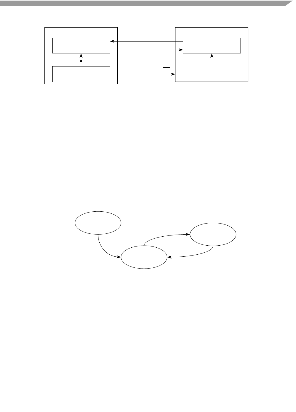
Functional Description
MCF548x Reference Manual, Rev. 3
Freescale Semiconductor 27-19
Figure 27-11. SPI Serial Protocol Overview
The DSPI has four peripheral chip select signals that are used to select which of the slaves to communicate
with: DSPICS5, DSPICS3, DSPICS1, and DSPICS0.
The transfer rate and delay settings are described in section Section 27.7.3, “DSPI Baud Rate and Clock
Delay Generation.”
27.7.1 Start and Stop of DSPI Transfers
The DSPI has two operating states; stopped and running. The states are independent of DSPI
configuration. The default state of the DSPI is stopped. In the stopped state, no serial transfers are initiated
in master mode and no transfers are responded to in slave mode. The stopped state is also a safe state for
writing the various configuration registers of the DSPI without causing undetermined results. The
DSR[TXRXS] bit is cleared in this state. In the running state, serial transfers take place. The
DSR[TXRXS] bit is set in the running state. Figure 27-12 shows a state diagram of the start and stop
mechanism. The transitions are described in Table 27-14.
Figure 27-12. DSPI Start and Stop State Diagram
DSPI Master
Shift Register
Baud Rate Generator
DSPI Slave
Shift Register
SOUTDSPISIN
DSPISOUT SIN
DSPISCK SCK
DSPICSnSS
Running
TXRXS=1
Stopped
TXRXS=0
Reset
Power-On-Reset 0
1
2

MCF548x Reference Manual, Rev. 3
27-20 Freescale Semiconductor
State transitions from running to stopped occur on the next frame boundary if a transfer is in progress, or
on the next system clock cycle if no transfers are in progress.
27.7.2 Serial Peripheral Interface (SPI)
The SPI transfers data serially using a shift register and a selection of programmable transfer attributes.
The SPI frames can be from 4 to 16 bits long. The data to be transmitted can come from queues stored in
RAM external to the DSPI. Host software or the DMA controller can transfer the SPI data from the queues
to a FIFO. The received data is stored in entries in the receive FIFO (Rx FIFO) buffer. Host software or
the DMA controller transfer the received data from the Rx FIFO to memory external to the DSPI. The
FIFO buffer operations are described in Section 27.7.2.4, “Tx FIFO Buffering Mechanism” and
Section 27.7.2.5, “Rx FIFO Buffering Mechanism.” The interrupt and DMA request conditions are
described in Section 27.7.6, “Interrupts/DMA Requests.”
The SPI supports two block-specific modes: master mode and slave mode. The FIFO operations are similar
for both modes. The main difference is that in master mode the DSPI initiates and controls the transfer
according to the fields in the SPI command field of the Tx FIFO entry. In slave mode, the DSPI only
responds to transfers initiated by a bus master external to the DSPI, and the SPI command field of the Tx
FIFO entry is ignored.
27.7.2.1 Master Mode
In SPI master mode, the DSPI initiates the serial transfers by controlling the serial communications clock
(DSPISCK) and the peripheral chip select (DSPICSn) signals. The SPI command field in the executing Tx
FIFO entry determines which DCTAR register will be used to set the transfer attributes and which
DSPICSn signals to assert. The command field also contains various bits that help with queue management
and transfer protocol. See Section 27.6.6, “DSPI Tx FIFO Register (DTFR)” for details on the SPI
command fields. The data field in the executing Tx FIFO entry is loaded into the shift register and shifted
out on the serial out (DSPISOUT) pin. In SPI master mode, each SPI frame to be transmitted has a
command associated with it, allowing for transfer attribute control on a frame-by-frame basis.
27.7.2.2 Slave Mode
In SPI slave mode, the DSPI responds to transfers initiated by an SPI bus master. The DSPI does not
initiate transfers. Certain transfer attributes such as clock polarity, clock phase, and frame size must be set
Table 27-14. State Transitions for Start and Stop of DSPI Transfers
Transition # Current State Next State Description
0 Reset Stopped Generic power-on-reset transition
1 Stopped Running The DSPI is started (DSPI transitions to Running) when all of the following
conditions are true:
• EOQF bit is clear
• Debug mode is unselected or the FRZ bit is clear
• HALT bit is clear
2 Running Stopped The DSPI stops (transitions from Running to Stopped) after the current frame
for any one of the following conditions:
• EOQF bit is set
• Debug mode is selected and the FRZ bit is set
• HALT bit is set

Functional Description
MCF548x Reference Manual, Rev. 3
Freescale Semiconductor 27-21
for successful communication with an SPI master. These SPI slave mode transfer attributes are set in the
DCTAR0.
27.7.2.3 FIFO Disable Operation
The FIFO disable mechanisms allow SPI transfers without using the Tx FIFO or Rx FIFO. The DSPI
operates as a double-buffered simplified SPI when the FIFOs are disabled. The Tx and Rx FIFOs are
disabled separately. The Tx FIFO is disabled by setting DMCR[DTXF]. The Rx FIFO is disabled by
setting DMCR[DRXF].
The FIFO disable mechanisms are transparent to the user and to host software; transmit data and
commands are written to the DTFR and received data is read from the DRFR.When the Tx FIFO is
disabled, the TFFF, TFUF, and TXCTR fields in DSR behave as if there is a one-entry FIFO, but the
contents of the DTFDR registers and DSR[TXPTR] are undefined. When the Rx FIFO is disabled, the
RFDF, RFOF, and RXCTR fields in the DSR behave as if there is a one-entry FIFO, but the contents of
the DRFDR registers and DSR[RXPTR] are undefined.
27.7.2.4 Tx FIFO Buffering Mechanism
The Tx FIFO functions as a buffer of SPI data and SPI commands for transmission. The Tx FIFO holds
from 1 to 16 longwords, each consisting of a command field and a data field. SPI commands and data are
added to the Tx FIFO by writing to the DTFR. Tx FIFO entries can only be removed from the Tx FIFO by
being shifted out or by flushing the Tx FIFO.
The DSR[TXCTR] field indicates the number of valid entries in the Tx FIFO. The TXCTR is updated
every time the DTFR is written or when SPI data is transferred into the shift register from the Tx FIFO.
The DSR[TXPTR] field indicates which Tx FIFO entry will be transmitted during the next transfer. The
TXPTR contains the positive offset from DTFDR0 in the number of 32-bit registers. For example, TXPTR
equal to two means that the DTFDR2 contains the SPI data and command for the next transfer. The TXPTR
field is incremented every time SPI data is transferred from the Tx FIFO to the shift register.
27.7.2.4.1 Filling the Tx FIFO
Host software or other intelligent blocks can add (push) entries to the Tx FIFO by writing to the DTFR.
When the Tx FIFO is not full, the Tx FIFO fill flag (DSR[TFFF]) is set. The TFFF bit is cleared when Tx
FIFO is full and the DMA controller indicates that a write to DTFR is complete or by host software writing
a ‘1’ to the DSR[TFFF]. The TFFF can generate a DMA request or an interrupt request. See
Section 27.7.6.2, “Transmit FIFO Fill Interrupt or DMA Request” for details.
The DSPI ignores attempts to push data to a full Tx FIFO, i.e. the state of the Tx FIFO is unchanged. No
error condition is indicated.
27.7.2.4.2 Draining the Tx FIFO
The Tx FIFO entries are removed (drained) by shifting SPI data out through the shift register. Entries are
transferred from the Tx FIFO to the shift register and shifted out, as long as there are valid entries in the
Tx FIFO. Every time an entry is transferred from the Tx FIFO to the shift register, the Tx FIFO counter is
decremented by one. At the end of a transfer, the DSR[TCF] bit is set to indicate the completion of a
transfer. The Tx FIFO is flushed by setting the DMCR[CTXF] bit.
If an external bus master initiates a transfer with a DSPI slave while the slave’s DSPI Tx FIFO is empty,
the Tx FIFO underflow flag (DSR[FUF]) is set. See Section 27.7.6.4, “Transmit FIFO Underflow Interrupt
Request” for details.

MCF548x Reference Manual, Rev. 3
27-22 Freescale Semiconductor
27.7.2.5 Rx FIFO Buffering Mechanism
The Rx FIFO functions as a buffer for data received on the DSPISIN signal. The Rx FIFO holds from 1 to
16 received SPI data frames. SPI data is added to the Rx FIFO at the completion of a transfer when the
received data in the shift register is transferred into the Rx FIFO. SPI data is removed (popped) from the
Rx FIFO by reading the DRFR. Rx FIFO entries can only be removed from the Rx FIFO by reading the
DRFR or by flushing the Rx FIFO.
The Rx FIFO counter field (DSR[RXCTR]) indicates the number of valid entries in the Rx FIFO. The
RXCTR is updated every time the DRFR is read or when SPI data is copied from the shift register to the
Rx FIFO.
The DSR[RXPTR] field points to the Rx FIFO entry that is returned when the DRFR is read. The RXPTR
contains the positive offset from DRFDR0 in the number of 32-bit registers. For example, RXPTR equal
to two means that the DRFDR2 contains the received SPI data that will be returned when DRFR is read.
The RXPTR field is incremented every time the DRFR is read.
27.7.2.5.1 Filling the Rx FIFO
The Rx FIFO is filled with the received SPI data from the shift register. While the Rx FIFO is not full, SPI
frames from the shift register are transferred to the Rx FIFO. Every time an SPI frame is transferred to the
Rx FIFO, the Rx FIFO counter is incremented by one.
If the Rx FIFO and shift register are full and a transfer is initiated, the DSR[RFOF] bit is set indicating an
overflow condition. Depending on the state of the DMCR[ROOE] bit, the data from the transfer that
generated the overflow is either ignored or shifted into the shift register. If the ROOE bit is set, the
incoming data is shifted into the shift register and data is overwritten. If the ROOE bit is cleared, the
incoming data is ignored.
27.7.2.5.2 Draining the Rx FIFO
Host software or the DMA controller can remove (pop) entries from the Rx FIFO by reading the DRFR.
A read of the DRFR decrements the Rx FIFO counter by one. Attempts to pop data from an empty Rx FIFO
are ignored, the Rx FIFO counter remains unchanged. The data returned from reading an empty Rx FIFO
is undetermined.
When the Rx FIFO is not empty, the Rx FIFO drain flag (DSR[RFDF]) is set. The RFDF bit is cleared
when the Rx FIFO is empty and the DMA controller indicates that a read from DRFR is complete or by
host software writing a ‘1’ to the RFDF.
27.7.3 DSPI Baud Rate and Clock Delay Generation
The DSPISCK frequency and the delay values for serial transfer are generated by dividing the system
clock frequency by a prescaler and a scaler. Figure 27-13 shows conceptually how the DSPISCK signal is
generated. For the MCF548x, the clock rate is 100 MHz.
Figure 27-13. Communications Clock Prescalers and Scalers
DSPISCK
System Clock Prescaler
1
Scaler
1

Functional Description
MCF548x Reference Manual, Rev. 3
Freescale Semiconductor 27-23
27.7.3.1 Baud Rate Generator
The baud rate is the frequency of the DSPI serial communication clock (DSPISCK). The system clock fsys
is divided by a prescaler (PBR) and scaler (BR) to produce DSPISCK. The PBR and BR fields in the
DCTARn registers select the frequency of DSPISCK by the formula below:
Table 27-15 shows an example of how to compute the baud rate.
27.7.3.2 CS to SCK Delay (tCSC)
The CS to SCK delay is the length of time from assertion of the DSPICSn signal to the first DSPISCK
edge. See Figure 27-17 for an illustration of the CS to SCK delay. The PCSSCK and CSSCK fields in the
DCTARn registers select the CS to SCK delay by the formula below:
Eqn. 27-5
Table 27-16 shows an example of how to compute the CS to SCK delay.
27.7.3.3 After DSPISCK Delay (tASC)
The after DSPISCK delay is the length of time between the last edge of DSPISCK and the negation of
DSPICSn. See Figure 27-15 and Figure 27-16 for illustrations of the after DSPISCK delay. The PASC and
ASC fields in the DCTARn registers select the after DSPISCK delay by the formula below:
Eqn. 27-6
Table 27-17 shows an example of how to compute the after DSPISCK delay.
27.7.3.4 Delay after Transfer (tDT)
The delay after transfer is the length of time between negation of the DSPICSn signal for a frame and the
assertion of the DSPICSn signal for the next frame. See Figure 27-15 for an illustration of the delay after
transfer. The PDT and DT fields in the DCTARn registers select the delay after transfer by the formula
below:
Table 27-15. Baud Rate Computation Example
PBR Prescaler BR Scaler Fsys Baud Rate
0b00 2 0b0000 2 100 MHz 25 Mb/s
Table 27-16. PCS to DSPISCK Delay Computation Example
PCSSCK Prescaler CSSCK Scaler Fsys PCS to DSPISCK
Delay
0b01 3 0b0100 32 100 MHz 0.96 us
Table 27-17. After DSPISCK Delay Computation Example
PASC Prescaler ASC Scaler Fsys After DSPISCK Delay
0b01 3 0b0100 32 100 MHz 0.96 us
DSPISCK baud rate =
PBR × BR
fsys
tCSC
1
fsys
--------PCSSCK CSSCK××=
tASC
1
fsys
--------PASC×ASC×=
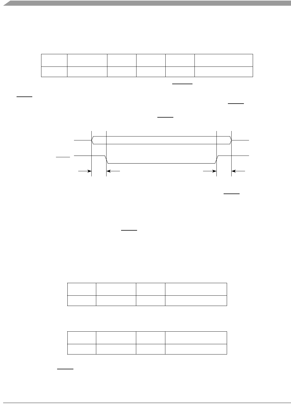
MCF548x Reference Manual, Rev. 3
27-24 Freescale Semiconductor
Eqn. 27-7
Table 27-18 shows an example of how to compute the delay after transfer.
27.7.3.5 Peripheral Chip Select Strobe Enable (PCSS)
The PCSS signal provides a delay to allow the DSPICSn signals to settle after transitioning, thereby
avoiding glitches. When the DSPI is in master mode and DMCR[PCSSE] bit is set, PCSS provides a signal
for an external demultiplexer to decode the DSPICSn[0,2:3] signals into as many as eight glitch-free
DSPICSn signals. Figure 27-14 shows the timing of the PCSS signal relative to PCS signals.
Figure 27-14. Peripheral Chip Select Strobe Timing
The delay between the assertion of the DSPICSn signals and the assertion of PCSS is selected by the
PCSSCK field in the DCTARn based on the following formula:
Eqn. 27-8
At the end of the transfer the delay between PCSS negation and DSPICSn negation is selected by the PASC
field in the DCTARn based on the following formula:
Eqn. 27-9
Table 27-19 shows an example of how to compute the tpcssck delay.
Table 27-20 shows an example of how to compute the tpasc delay.
NOTE
The PCSS signal is not supported when continuous DSPISCK is enabled
(CONT=1).
Table 27-18. Delay after Transfer Computation Example
PDT Prescaler DT Scaler Fsys Delay after Transfer
0b01 3 0b1110 32768 100 MHz 0.98 ms
Table 27-19. Peripheral Chip Select Strobe Assert Computation Example
PCSSCK Prescaler Fsys Delay before Transfer
0b11 7 100 MHz 70.0 ns
Table 27-20. Peripheral Chip Select Strobe Negate Computation Example
PASC Prescaler Fsys Delay after Transfer
0b11 7 100 MHz 70.0 ns
tDT
1
fsys
--------PDT×DT×=
PCSS
DSPICSn
tPCSSCK tPASC
tPCSSCK
1
fsys
--------PCSSCK×=
tPASC
1
fsys
--------PASC×=

Functional Description
MCF548x Reference Manual, Rev. 3
Freescale Semiconductor 27-25
27.7.4 Transfer Formats
The SPI serial communication is controlled by the serial communications clock (DSPISCK) signal and the
DSPICSn signals. The DSPISCK signal provided by the master device synchronizes shifting and sampling
of the data on the DSPISIN and DSPISOUT pins. The DSPICSn signals serve as enable signals for the
slave devices.
When the DSPI is the bus master, the CPOL and CPHA bits in the DSPI clock and transfer attributes
registers (DCTARn) select the polarity and phase of the clock. The polarity bit selects the idle state of
DSPISCK. The clock phase bit selects if the data on DSPISOUT is valid before or on the first DSPISCK
edge.
When the DSPI is the bus slave, CPOL and CPHA bits in the DCTAR0 select the polarity and phase of the
serial clock. Even though the bus slave does not control the DSPISCK signal, the clock polarity, clock
phase, and number of bits to transfer settings for both the master and slave must be identical to ensure
proper transmission.
The DSPI supports four different transfer formats:
• Classic SPI with CPHA = 0
• Classic SPI with CPHA = 1
• Modified transfer format with CPHA = 0
• Modified transfer format with CPHA = 1
A modified transfer format is supported to allow for high-speed communication with peripherals that
require longer setup times. The DSPI can sample the incoming data later than halfway through the cycle
to give the peripheral more setup time. The DMCR[MTFE] bit selects between classic SPI format and
modified transfer format. The modified transfer formats are described in Section 27.7.4.3, “Modified SPI
Transfer Format (MTFE = 1, CPHA = 0)” and Section 27.7.4.4, “Modified SPI Transfer Format (MTFE =
1, CPHA = 1).”
The classic SPI formats are described in Section 27.7.4.1, “Classic SPI Transfer Format (CPHA = 0)” and
Section 27.7.4.2, “Classic SPI Transfer Format (CPHA = 1).”
The DSPI provides the option of keeping the DSPICSn signals asserted between frames. See
Section 27.7.4.5, “Continuous Selection Format” for details.
27.7.4.1 Classic SPI Transfer Format (CPHA = 0)
The transfer format shown in Figure 27-15 is used to communicate with peripheral SPI slave devices
where the first data bit is available on the first clock edge. In this format, the master and slave sample their
DSPISIN pins on the odd-numbered DSPISCK edges and change the data on their DSPISOUT pins on the
even-numbered DSPISCK edges.
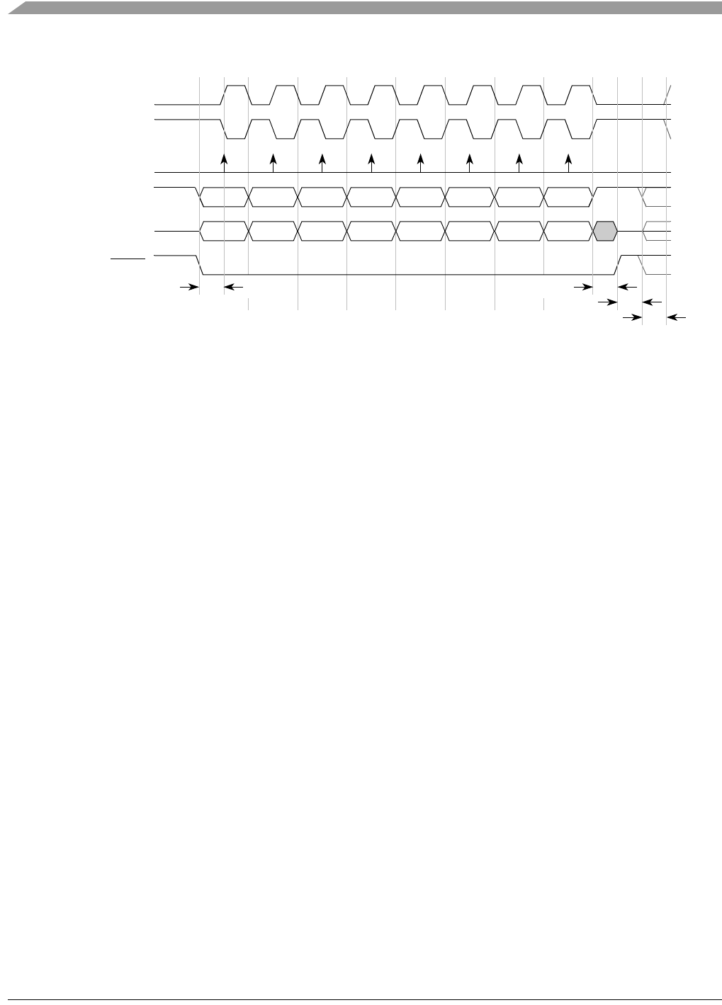
MCF548x Reference Manual, Rev. 3
27-26 Freescale Semiconductor
Figure 27-15. DSPI Transfer Timing Diagram (MTFE = 0, CPHA = 0, FMSZ = 8)
The master initiates the transfer by placing its first data bit on the DSPISOUT pin and asserting the
appropriate peripheral chip select signals to the slave device. The slave responds by placing its first data
bit on its DSPISOUT pin. After the tCSC delay has elapsed, the master outputs the first edge of DSPISCK.
This is the edge used by the master and slave devices to sample the first input data bit on their serial data
input signals. At the second edge of the DSPISCK, the master and slave devices place their second data
bit on their serial data output signals. For the rest of the frame, the master and the slave sample their
DSPISIN pins on the odd-numbered clock edges and change the data on their DSPISOUT pins on the
even-numbered clock edges. After the last clock edge occurs, a delay of tASC is inserted before the master
negates the CSn signals. A delay of tDT is inserted before a new frame transfer can be initiated by the
master.
27.7.4.2 Classic SPI Transfer Format (CPHA = 1)
This transfer format shown in Figure 27-16 is used to communicate with peripheral SPI slave devices that
require the first DSPISCK edge before the first data bit becomes available on the slave DSPISOUT pin. In
this format the master and slave devices change the data on their DSPISOUT pins on the odd-numbered
DSPISCK edges and sample the data on their DSPISIN pins on the even-numbered DSPISCK edges
DSPISCK
12345678910111213141516
(CPOL = 0)
DSPICSn/PCSS
tASC
DSPISCK
(CPOL = 1)
Master and Slave
Sample
Master DSPISOUT/
Slave DSPISIN
Master DSPISIN/
Slave DSPISOUT
Bit 6
Bit 1 Bit 5
Bit 2 Bit 4
Bit 3 Bit 3
Bit 4 Bit 2
Bit 5 Bit 1
Bit 6 LSB
MSB
MSB
LSB
tDTtCSC
tCSC
MSB First (LSBFE = 0):
LSB First (LSBFE = 1):
tCSC = PCS to DSPISCK delay
tASC = After DSPISCK delay
tDT = Delay after transfer (minimum CS idle time)

Functional Description
MCF548x Reference Manual, Rev. 3
Freescale Semiconductor 27-27
Figure 27-16. DSPI Transfer Timing Diagram (MTFE = 0, CPHA = 1, FMSZ = 8)
The master initiates the transfer by asserting the CSn signal to the slave. After the tCSC delay has elapsed,
the master generates the first DSPISCK edge and, at the same time, places valid data on the master
DSPISOUT pin. The slave responds to the first DSPISCK edge by placing its first data bit on its slave
DSPISOUT pin.
At the second edge of the DSPISCK, the master and slave sample their DSPISIN pins. For the rest of the
frame, the master and the slave change the data on their DSPISOUT pins on the odd-numbered clock edges
and sample their DSPISIN pins on the even-numbered clock edges. After the last clock edge occurs, a
delay of tASC is inserted before the master negates the PCSS signal. A delay of tDT is inserted before a new
frame transfer can be initiated by the master.
27.7.4.3 Modified SPI Transfer Format (MTFE = 1, CPHA = 0)
In this modified transfer format, both the master and the slave sample later in the DSPISCK period than in
classic SPI mode to allow for delays in device pads and board traces. These delays become a more
significant fraction of the DSPISCK period as the DSPISCK period decreases with increasing baud rates.
The master and the slave place data on the DSPISOUT pins at the assertion of the CSn signal. After the
CSn to DSPISCK delay has elapsed the first DSPISCK edge is generated. The slave samples the master
DSPISOUT signal on every odd numbered DSPISCK edge. The slave also places new data on the slave
DSPISOUT on every odd numbered clock edge.
The master places its second data bit on the DSPISOUT line one system clock after odd numbered
DSPISCK edge. The point where the master samples the slave DSPISOUT is selected by writing to the
DMCR[SMPL_PT] field lists the number of system clock cycles between the active edge of DSPISCK and
the master sample point. The master sample point can be delayed by one or two system clock cycles.
Figure 27-17 shows the modified transfer format for CPHA = 0. Only the condition where CPOL = 0 is
illustrated. The delayed master sample points are indicated with a lighter shaded arrow.
DSPISCK
12345678910111213141516
(CPOL = 0)
DSPICSn/PCSS
tASC
DSPISCK
(CPOL = 1)
Master and Slave
Sample
Master DSPISOUT/
Slave DSPISIN
Master DSPISIN/
Slave DSPISOUT
Bit 6
Bit 1 Bit 5
Bit 2 Bit 4
Bit 3 Bit 3
Bit 4 Bit 2
Bit 5 Bit 1
Bit 6 LSB
MSB
MSB
LSB
tDT
tCSC
MSB First (LSBFE = 0):
LSB First (LSBFE = 1):
tCSC = PCSS to DSPISCK delay
tASC = After DSPISCK delay
tDT = Delay after transfer (minimum CS negation time)
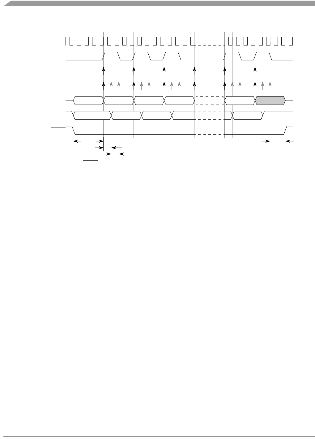
MCF548x Reference Manual, Rev. 3
27-28 Freescale Semiconductor
Figure 27-17. DSPI Modified Transfer Format (MTFE = 1, CPHA = 0, Fsck = Fsys/4)
27.7.4.4 Modified SPI Transfer Format (MTFE = 1, CPHA = 1)
Figure 27-18 shows the modified transfer format for CPHA = 1. Only the condition where CPOL = 0 is
described. At the start of a transfer the DSPI asserts the CSn signal to the slave device. After the CS to
DSPISCK delay has elapsed, the master and the slave put data on their DSPISOUT pins at the first edge
of DSPISCK. The slave samples the master DSPISOUT signal on the even numbered edges of DSPISCK.
The master samples the slave DSPISOUT signal on the odd numbered DSPISCK edges, starting with the
third DSPISCK edge. The slave samples the last bit on the last edge of the DSPISCK. The master samples
the last slave DSPISOUT bit one-half DSPISCK cycle after the last edge of DSPISCK. No clock edge will
tCSC = PCSS to DSPISCK delay
tASC = After DSPISCK delay
System Clock
123456
PCSS
tASC
DSPISCK
Master Sample
Slave DSPISOUT
Master DSPISOUT
System Clock
System Clock
Slave Sample
tCSC
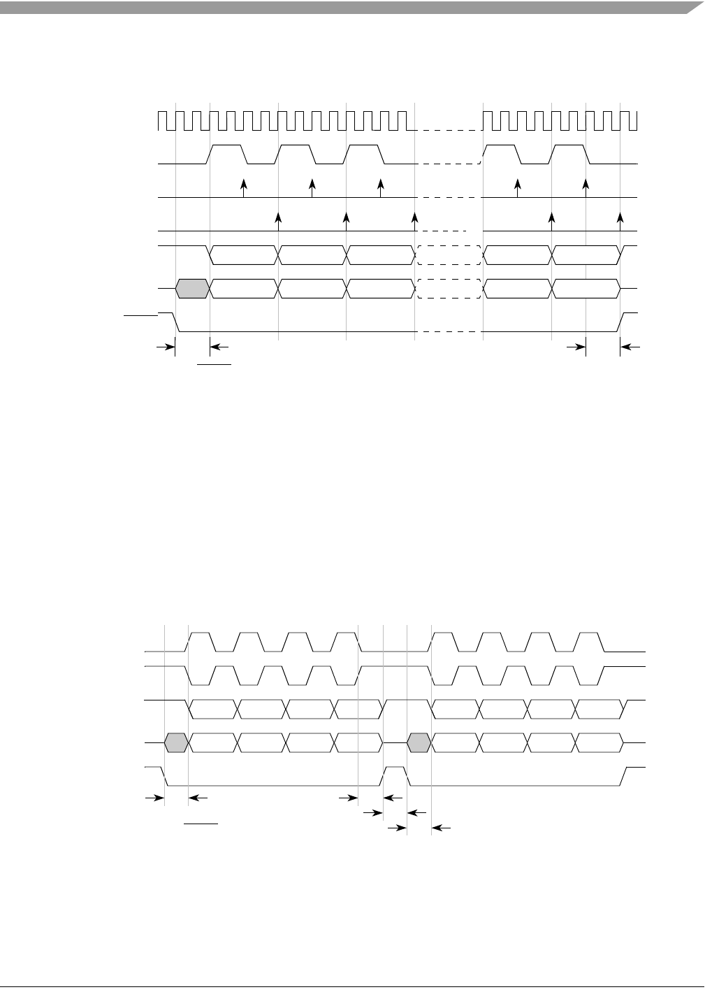
Functional Description
MCF548x Reference Manual, Rev. 3
Freescale Semiconductor 27-29
be visible on the master DSPISCK pin during the sampling of the last bit. The DSPISCK to CS delay must
be greater or equal to half of the DSPISCK period.
Figure 27-18. DSPI Modified Transfer Format
(MTFE = 1, CPHA = 1, Fsck = Fsys/4)
27.7.4.5 Continuous Selection Format
Some peripherals must be deselected between every transfer. Other peripherals must remain selected
between several sequential serial transfers. The continuous selection format provides the flexibility to
handle both cases. The continuous selection format is enabled by setting the DTFR[CONT].
When the CONT bit = 0, the DSPI drives the asserted chip select signals to their idle states in between
frames. The idle states of the chip select signals are selected by the DMCR[PCSIS] field. Figure 27-19
shows the timing diagram for two 4-bit transfers with CPHA = 1 and CONT = 0.
Figure 27-19. Example of Non-Continuous Format (CPHA = 1, CONT = 0)
When the CONT bit = 1 and the DSPICSn signal for the next transfer is the same as for the current transfer,
the DSPICSn signal remains asserted for the duration of the two transfers. The delay between transfers
tCSC = PCSS to DSPISCK delay
tASC = After DSPISCK delay
System Clock
123456
PCSS
tASC
DSPISCK
Master Sample
Master DSPISOUT
Slave DSPISOUT
Slave Sample
tCSC
DSPISCK
(CPOL = 0)
CSn
tASC
DSPISCK
(CPOL = 1)
Master DSPISOUT
tDT
tCSC
tCSC = PCSS to DSPISCK delay
tASC = After DSPISCK delay
tDT = Delay after transfer (minimum CS negation time)
Master DSPISIN
tCSC

MCF548x Reference Manual, Rev. 3
27-30 Freescale Semiconductor
(tDT) is not inserted between the transfers. Figure 27-20 shows the timing diagram for two 4-bit transfers
with CPHA = 1 and CONT = 1.
Figure 27-20. Example of Continuous Transfer (CPHA = 1, CONT = 1)
Switching DCTARn registers between frames while using continuous selection can cause errors in the
transfer. The DSPICSn signal must be negated before DCTARn is switched.
When the CONT bit = 1 and the DSPICSn signals for the next transfer are different from the present
transfer, the DSPICSn signals behave as if the CONT bit was not set.
27.7.5 Continuous Serial Communications Clock
The DSPI provides the option of generating a continuous DSPISCK signal for slave peripherals that
require a continuous clock.
Continuous DSPISCK is enabled by setting DMCR[CSCK]. Continuous DSPISCK is only supported for
CPHA = 1. Setting CPHA = 0 will be ignored if the CSCK bit is set. Continuous DSPISCK is supported
for modified transfer format.
Clock and transfer attributes for the continuous DSPISCK mode are set according to the following rules:
• DCTAR0 is used initially. At the start of each SPI frame transfer, the DCTARn specified by the
CTAS for the frame shall be used.
• The currently selected DCTARn remains in use until the start of a frame with a different DCTARn
specified, or the continuous DSPISCK mode is terminated.
It is recommended that the baud rate is the same for all transfers made while using the continuous
DSPISCK. Switching clock polarity between frames while using continuous DSPISCK can cause errors
in the transfer. Continuous DSPISCK operation is not guaranteed if the DSPI is put into the external stop
mode or module disable mode.
Enabling continuous DSPISCK disables the CS to DSPISCK delay and the after DSPISCK delay. The
delay after transfer is fixed at one DSPISCK cycle. Figure 27-21 shows timing diagram for continuous
DSPISCK format with continuous selection disabled.
DSPISCK
(CPOL = 0)
PCSS
tASC
DSPISCK
(CPOL = 1)
Master DSPISOUT
tCSC
tCSC
tCSC = PCSS to DSPISCK delay
tASC = After DSPISCK delay
Master DSPISIN
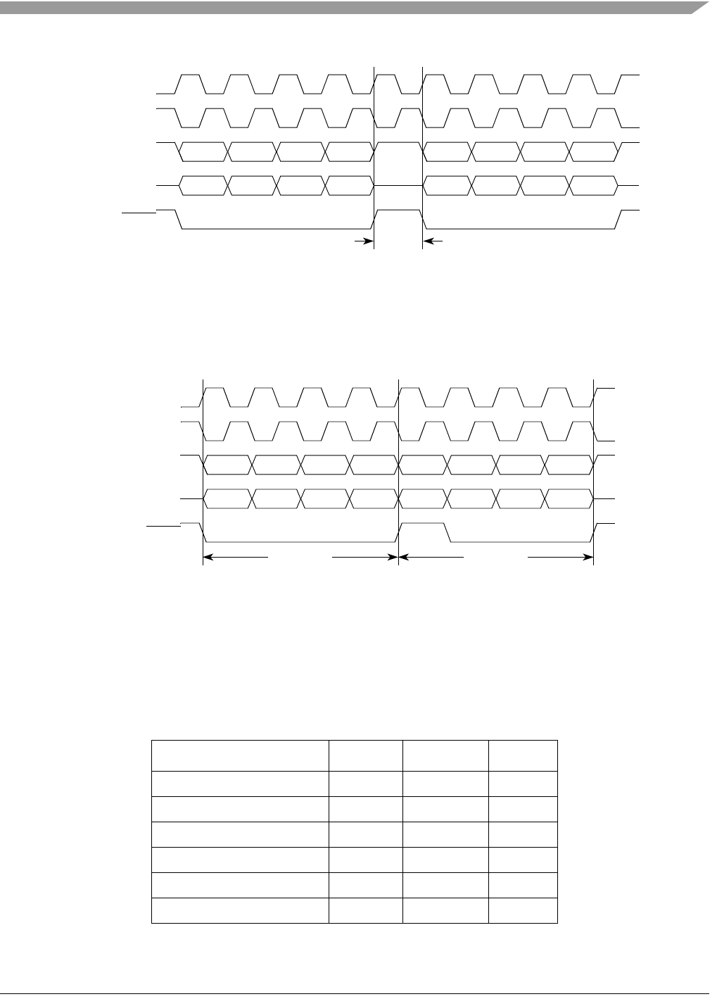
Functional Description
MCF548x Reference Manual, Rev. 3
Freescale Semiconductor 27-31
Figure 27-21. Continuous DSPISCK Timing Diagram (CSCK = 0)
If DTFR[CONT] is set, DSPICSn remains asserted between the transfers when the DSPICSn signal for the
next transfer is the same as for the current transfer. Figure 27-22 shows timing diagram for continuous
DSPISCK format with continuous selection enabled.
Figure 27-22. Continuous DSPISCK Timing Diagram (CSCK = 1)
27.7.6 Interrupts/DMA Requests
The DSPI has four conditions that can only generate interrupt requests and two conditions that can
generate either an interrupt or DMA request. Table 27-21 lists the six conditions.
Table 27-21. Interrupt and DMA Request Conditions
Condition Flag Interrupt DMA
End of Queue EOQF X
TX FIFO Fill TFFF X X
Transfer Complete TCF X
TX FIFO Underflow TFUF X
RX FIFO Drain RFDF X X
RX FIFO Overflow RFOF X
DSPISCK
(CPOL = 0)
PCSS
DSPISCK
(CPOL = 1)
Master DSPISOUT
tDT
tDT = 1 DSPISCK
Master DSPISIN
DSPISCK
(CPOL = 0)
PCSS
DSPISCK
(CPOL = 1)
Master DSPISOUT
Master DSPISIN
Transfer 1 Transfer 2

MCF548x Reference Manual, Rev. 3
27-32 Freescale Semiconductor
Each condition has a flag bit in the Section 27.6.4, “DSPI Status Register (DSR)” and a request enable bit
in the Section 27.6.5, “DSPI DMA/Interrupt Request Select Register (DIRSR).” The Tx FIFO fill flag
(TFFF) and Rx FIFO drain flag (RFDF) generate interrupt requests or DMA requests depending on the
DIRSR[TFFFS] and DIRSR[RFDFS] bits.
27.7.6.1 End of Queue Interrupt Request
The end of queue request indicates that the end of a transmit queue is reached. The end of queue request
is generated when the EOQ bit in the executing SPI command is set and the DIRSR[EOQFE] bit is set.
27.7.6.2 Transmit FIFO Fill Interrupt or DMA Request
The Tx FIFO fill request indicates that the Tx FIFO is not full. The Tx FIFO fill request is generated when
the number of entries in the Tx FIFO is less than the maximum number of possible entries, and the
DIRSR[TFFFE] bit is set. The DIRSR[TFFFS] bit selects whether a DMA request or an interrupt request
is generated.
27.7.6.3 Transfer Complete Interrupt Request
The transfer complete request indicates the end of the transfer of a serial frame. The transfer complete
request is generated at the end of each frame transfer when the DIRSR[TCF_RE] bit is set.
27.7.6.4 Transmit FIFO Underflow Interrupt Request
The Tx FIFO underflow request indicates that an underflow condition in the Tx FIFO has occurred. The
transmit underflow condition is detected only for DSPI blocks operating in slave mode and SPI
configuration. The TFUF bit is set when the Tx FIFO of a DSPI operating in slave mode and SPI
configuration is empty, and a transfer is initiated from an external SPI master. If the TFUF bit is set while
the DIRSR[TFUFE] bit is set, an interrupt request is generated.
27.7.6.5 Receive FIFO Drain Interrupt or DMA Request
The Rx FIFO drain request indicates that the Rx FIFO is not empty. The Rx FIFO drain request is
generated when the number of entries in the Rx FIFO is not zero, and the DIRSR[RFDFE] bit is set. The
DIRSR[RFDFS] bit selects whether a DMA request or an interrupt request is generated.
27.7.6.6 Receive FIFO Overflow Interrupt Request
The Rx FIFO overflow request indicates that an overflow condition in the Rx FIFO has occurred. An Rx
FIFO overflow request is generated when Rx FIFO and shift register are full and a transfer is initiated. The
DIRSR[RFOFE] bit must be set for the interrupt request to be generated.
Depending on the state of the DMCR[ROOE] bit, the data from the transfer that generated the overflow is
either ignored or shifted into the shift register. If the ROOE bit is set, the incoming data is shifted into the
shift register. If the ROOE bit is negated, the incoming data is ignored.

Initialization and Application Information
MCF548x Reference Manual, Rev. 3
Freescale Semiconductor 27-33
27.8 Initialization and Application Information
27.8.1 How to Change Queues
This section presents an example of how to change queues for the DSPI. The queues are not part of the
DSPI, but the DSPI includes features in support of queue management.
1. The last command word from a queue is executed. The EOQ bit in the command word is set to
indicate to the DSPI that this is the last entry in the queue.
2. At the end of the transfer corresponding to the command word with EOQ set, the EOQ flag
(EOQF) in the DSR is set.
3. The setting of the EOQF flag will disable both serial transmission, and serial reception of data,
putting the DSPI in the stopped state. The TXRXS bit is cleared to indicate the stopped state.
4. The DMA will continue to fill the Tx FIFO until it is full or step 5 occurs.
5. Disable DSPI DMA transfers by disabling the DMA enable request for the DMA channel
assigned to Tx FIFO and Rx FIFO. This is done by clearing the corresponding DMA enable
request bits in the DMA Controller.
6. Ensure all received data in the Rx FIFO has been transferred to memory receive queue by reading
the DSR[RXCNT] or by checking DSR[RFDF] after each read operation of the DRFR.
7. Modify DMA descriptor of Tx and Rx channels for new queues.
8. Flush the Tx FIFO by writing a ‘1’ to the DMCR[CLR_TXF] bit. Flush the Rx FIFO by writing a
‘1’ to the DMCR[CLR_RXF] bit.
9. Clear transfer count either by setting CTCNT bit in the command word of the first entry in the
new queue or via CPU writing directly to DTCR[SPI_TCNT] field.
10. Enable DMA channel by enabling the DMA enable request for the DMA channel assigned to the
DSPI Tx FIFO and/or setting the corresponding DMA enable request bit for the DMA channel
assigned to the Rx FIFO.
11. Enable serial transmission and serial reception of data by clearing the EOQF bit.
27.8.2 Baud Rate Settings
Table 27-22 shows the baud rate that is generated based on the combination of the baud rate prescaler PBR
and the baud rate scaler BR in the DCTARn registers. The values calculated assume a 100 MHz system
frequency.

MCF548x Reference Manual, Rev. 3
27-34 Freescale Semiconductor
27.8.3 Delay Settings
Table 27-23 shows the values for the delay after transfer (tDT) and CS to DSPISCK delay (tCSC) that can
be generated based on the prescaler values and the scaler values set in the DCTARn registers. The values
calculated assume a 100MHz system frequency.
Table 27-22. Baud Rate Values
Baud Rate Divider Prescaler Values
2357
Baud Rate Scaler Values
225.0MHz 16.7MHz 10.0MHz 7.14MHz
412.5MHz 8.33MHz 5.00MHz 3.57MHz
68.33MHz 5.56MHz 3.33MHz 2.38MHz
86.25MHz 4.17MHz 2.50MHz 1.79MHz
16 3.12MHz 2.08MHz 1.25MHz 893KHz
32 1.56MHz 1.04MHz 625KHz 446KHz
64 781KHz 521KHz 312KHz 223KHz
128 391KHz 260KHz 156KHz 112KHz
256 195KHz 130KHz 78.1KHz 55.8KHz
512 97.7KHz 65.1KHz 39.1KHz 27.9KHz
1024 48.8KHz 32.6KHz 19.5KHz 14.0KHz
2048 24.4KHz 16.3KHz 9.77KHz 6.98KHz
4096 12.2KHz 8.14KHz 4.88KHz 3.49KHz
8192 6.10KHz 4.07KHz 2.44KHz 1.74KHz
16384 3.05KHz 2.04KHz 1.22KHz 872
32768 1.53KHz 1.02KHz 610 436

Initialization and Application Information
MCF548x Reference Manual, Rev. 3
Freescale Semiconductor 27-35
27.8.4 Calculation of FIFO Pointer Addresses
The user has complete visibility of the Tx and Rx FIFO contents through the FIFO registers, and valid
entries can be identified through a memory mapped pointer and a memory mapped counter for each FIFO.
The pointer to the first-in entry in each FIFO is memory mapped. For the Tx FIFO the first-in pointer is
the transmit pointer (TXPTR). For the Rx FIFO the first-in pointer is the receive pointer (RXPTR).
Figure 27-23 illustrates the concept of first-in and last-in FIFO entries along with the FIFO counter. The
Tx FIFO is chosen for the illustration, but the concepts carry over to the Rx FIFO. See Section 27.7.2.4,
“Tx FIFO Buffering Mechanism” and Section 27.7.2.5, “Rx FIFO Buffering Mechanism” for details on
the FIFO operation.
Table 27-23. Delay Values
Delay Prescaler Values
1357
Delay Scaler Values
220.0 ns 60.0 ns 100.0 ns 140.0 ns
440.0 ns 120.0 ns 200.0 ns 280.0 ns
880.0 ns 240.0 ns 400.0 ns 560.0 ns
16 160.0 ns 480.0 ns 800.0 ns 1.1 µs
32 320.0 ns 960.0 ns 1.6 µs2.2 µs
64 640.0 ns 1.9 µs3.2 µs4.5 µs
128 1.3 µs3.8 µs6.4 µs9.0 µs
256 2.6 µs7.7 µs 12.8 µs 17.9 µs
512 5.1 µs 15.4 µs 25.6 µs 35.8 µs
1024 10.2 µs 30.7 µs 51.2 µs 71.7 µs
2048 20.5 µs 61.4 µs 102.4 µs 143.4 µs
4096 41.0 µs 122.9 µs 204.8 µs 286.7 µs
8192 81.9 µs 245.8 µs 409.6 µs 573.4 µs
16384 163.8 µs 491.5 µs 819.2 µs 1.1 ms
32768 327.7 µs 983.0 µs 1.6 ms 2.3 ms
65536 655.4 µs 2.0 ms 3.3 ms 4.6 ms
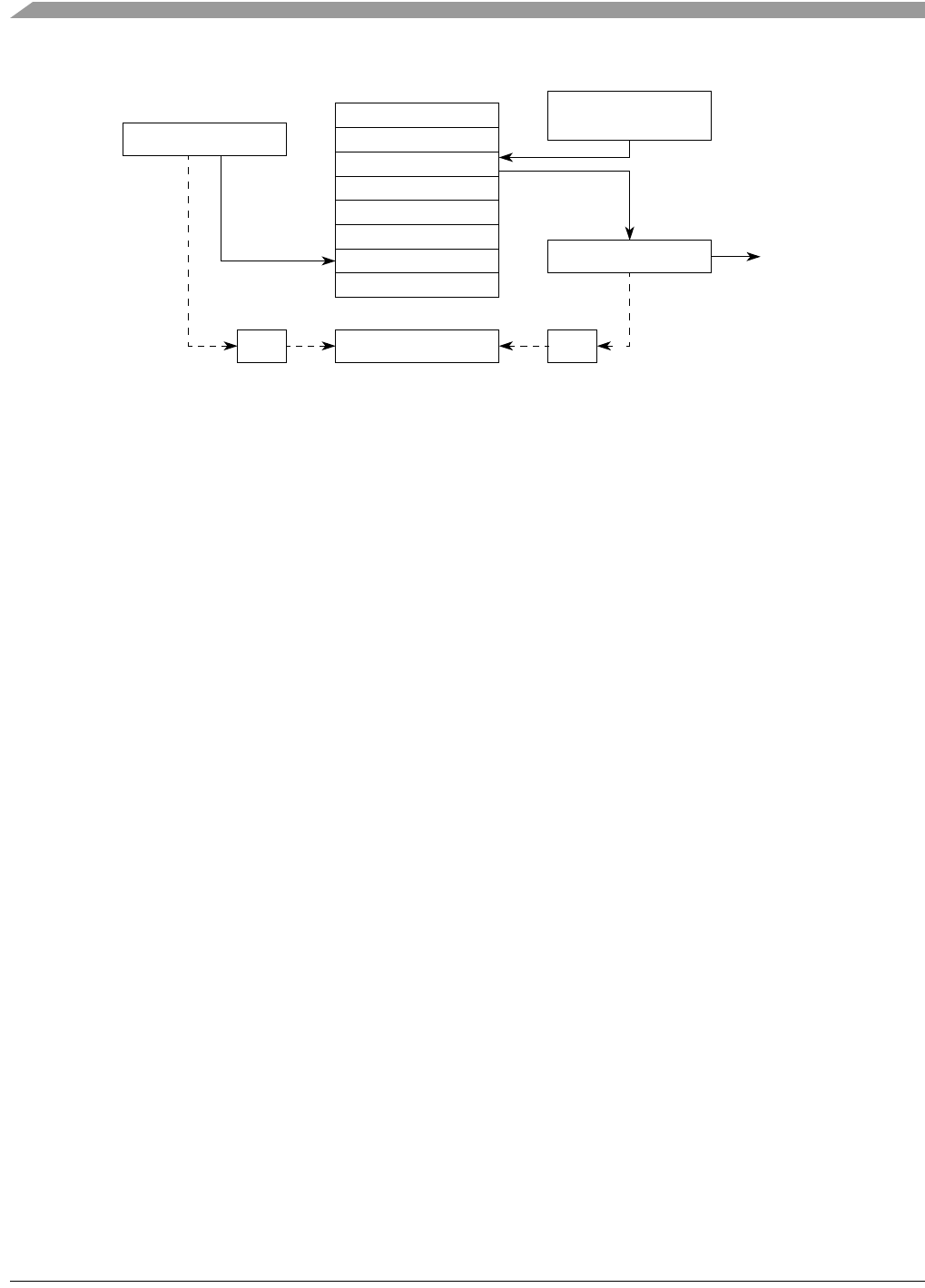
MCF548x Reference Manual, Rev. 3
27-36 Freescale Semiconductor
Figure 27-23. Tx FIFO Pointers and Counter
27.8.4.1 Address Calculation for the First-in Entry and Last-in Entry in the Tx FIFO
The memory address of the first-in entry in the Tx FIFO is computed by the following equation:
First-in entry address = Tx FIFO base + 4*(TXPTR)
The memory address of the last-in entry in the Tx FIFO is computed by the following equation:
Last-in entry address = Tx FIFO base + 4*[(TXCTR + TXPTR - 1)modulo 4]
Tx FIFO base - Base address of Tx FIFO
TXCTR - Tx FIFO counter
TXTPTR - Transmit pointer
27.8.4.2 Address Calculation for the First-in Entry and Last-in Entry in the Rx
FIFO
The memory address of the first-in entry in the Rx FIFO is computed by the following equation:
First-in entry address = Rx FIFO Base + 4*(RXPTR)
The memory address of the last-in entry in the Rx FIFO is computed by the following equation:
Last-in entry address = Rx FIFO base + 4*[(RXCTR + RXPTR - 1)modulo 4]
Rx FIFO base - Base address of RX FIFO
RXCTR - Rx FIFO counter
RXPTR - Receive pointer
Entry C
Entry A (First In)
– 1
Entry B
Entry D (Last In)
Tx FIFO Base
Tx FIFO Counter
Shift Register DSPISOUT
Transmit Data
Pointer
–
–
–
–
+ 1
Tx FIFO Register
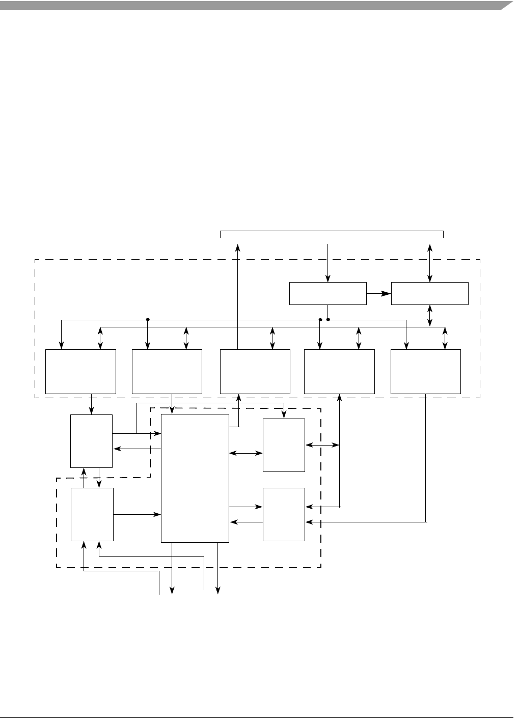
MCF548x Reference Manual, Rev. 3
Freescale Semiconductor 28-1
Chapter 28
I2C Interface
28.1 Introduction
This chapter describes the I2C™ module, including I2C protocol, clock synchronization, and I2C
programming model registers. It also provides extensive programming examples.
28.1.1 Block Diagram
A block diagram of the I2C module is shown in Figure 28-1.
Figure 28-1. I2C Block Diagram
Address
Compare
In/Out
Data
Shift
Start, Stop,
Input
Sync
Clock
Control
Registers and ColdFire Interface
Address Decode
I2C Address
Data MUX
SDASCL
Address
IRQ Data
and
Arbitration
Control
Register
Internal Bus
Register
(I2ADR)
I2C Frequency
Divider Register
(I2FDR)
I2C Data
I/O Register
(I2DR)
I2C Status
Register
(I2SR)
I2C Control
Register
(I2CR)
Functional
Module

MCF548x Reference Manual, Rev. 3
28-2 Freescale Semiconductor
28.1.2 I2C Overview
I2C is a two-wire, bidirectional serial bus which provides a simple, efficient method of data exchange
between devices. This two-wire bus minimizes the interconnection between the devices.
The interface is designed to operate up to 100 kbps with maximum bus loading and timing. The device is
capable of operating at higher baud rates, up to a maximum of clock/20, with reduced bus loading. The
maximum communication length and the number of devices that can be connected are limited by a
maximum bus capacitance of 400 pF.
This bus is suitable for applications requiring occasional communications over a short distance between a
number of devices. It also provides flexibility, allowing additional devices to be connected to the bus for
further expansion and system development.
I2C is a true multi-master bus including collision detection and arbitration to prevent data corruption if two
or more masters attempt to control the bus simultaneously. This feature provides the capability for complex
applications with multi-processor control. It may also be used for rapid testing and alignment of end
products via external connections to an assembly-line computer.
The MCF548x contains one I2C interface, with a dedicated set of pins.
28.1.3 Features
The I2C module has the following key features:
• Compatible with I2C bus standard
• Multi-master operation
• Software programmable for one of 50 different serial clock frequencies
• Software selectable acknowledge bit
• Interrupt driven byte-by-byte data transfer
• Arbitration lost interrupt with automatic mode switching from master to slave
• Calling address identification interrupt
• Start and stop signal generation/detection
• Repeated start signal generation
• Acknowledge bit generation/detection
• Bus busy detection
28.2 External Signals
The following table describes the external I2C signals
Table 28-1. I2C Signal Summary
Signal Name Direction Description
SCL I/O Open-drain clock signal for the I2C interface. Either it is driven by the I2C module when the bus
is in the master mode, or it becomes the clock input when the I2C is in the slave mode.
SDA I/O Open-drain signal that serves as the data input/output for the I2C interface.
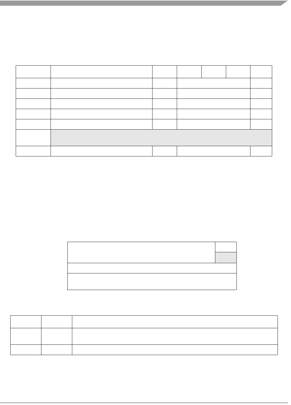
Memory Map/Register Definition
MCF548x Reference Manual, Rev. 3
Freescale Semiconductor 28-3
28.3 Memory Map/Register Definition
28.3.1 I2C Register Map
.
28.3.2 Register Descriptions
There are five registers used in the I2C interface with the interrupt control register. The internal
configuration of these registers is discussed in the following paragraphs.
28.3.2.1 I2C Address Register (I2ADR)
The I2ADR holds the address the I2C responds to when addressed as a slave. Note that it is not the address
sent on the bus during the address transfer.
Table 28-2. I2C Memory Map
MBAR Offset Name Byte0 Byte1 Byte2 Byte3 Access
0x8F00 I2C Address Register I2ADR — R/W
0x8F04 I2C Frequency Divider Register I2FDR — R/W
0x8F08 I2C Control Register I2CR — R/W
0x8F0C I2C Status Register I2SR — R/W
0x8F10 I2C Data I/O Register I2DR — R/W
0x8F14 –
0x8F1C
Reserved
0x8F20 I2C Interrupt Control Register I2ICR — R/W
76543210
RADR 0
W
Reset00000000
Reg
Addr
MBAR + 0x8F00
Figure 28-2. I2C Address Register (I2ADR)
Table 28-3. I2ADR Field Descriptions
Bits Name Description
7–1 ADR Slave address. Contains the specific slave address to be used by the I2C module.
Note: This is not the address sent on the bus during the address transfer.
0 — Reserved, should be cleared.

MCF548x Reference Manual, Rev. 3
28-4 Freescale Semiconductor
28.3.2.2 I2C Frequency Divider Register (I2FDR)
The I2FDR, shown in Figure 28-3, provides a programmable prescaler to configure the I2C clock for
bit-rate selection.
76543210
R0 0 IC
W
Reset00000000
Reg
Addr
MBAR + 0x8F04
Figure 28-3. I2C Frequency Divider Register (I2FDR)
Table 28-4. I2FDR Field Descriptions
Bits Name Description
7–6 — Reserved, should be cleared.
5–0 IC I2C clock rate. Prescales the clock for bit-rate selection. Due to potentially slow SCL and SDA rise
and fall times, bus signals are sampled at the prescaler frequency. The serial bit clock frequency is
equal to the system clock divided by the divider shown below.
IC Divider IC Divider IC Divider IC Divider
0x00 28 0x10 288 0x20 20 0x30 160
0x01 30 0x11 320 0x21 22 0x31 192
0x02 34 0x12 384 0x22 24 0x32 224
0x03 40 0x13 480 0x23 26 0x33 256
0x04 44 0x14 576 0x24 28 0x34 320
0x05 48 0x15 640 0x25 32 0x35 384
0x06 56 0x16 768 0x26 36 0x36 448
0x07 68 0x17 960 0x27 40 0x37 512
0x08 80 0x18 1152 0x28 48 0x38 640
0x09 88 0x19 1280 0x29 56 0x39 768
0x0A 104 0x1A 1536 0x2A 64 0x3A 896
0x0B 128 0x1B 1920 0x2B 72 0x3B 1024
0x0C 144 0x1C 2304 0x2C 80 0x3C 1280
0x0D 160 0x1D 2560 0x2D 96 0x3D 1536
0x0E 192 0x1E 3072 0x2E 112 0x3E 1792
0x0F 240 0x1F 3840 0x2F 128 0x3F 2048

Memory Map/Register Definition
MCF548x Reference Manual, Rev. 3
Freescale Semiconductor 28-5
28.3.2.3 I2C Control Register (I2CR)
The I2CR is used to enable the I2C module and the I2C interrupt. It also contains bits that govern operation
as a slave or a master.
28.3.2.4 I2C Status Register (I2SR)
This I2SR contains bits that indicate transaction direction and status.
76543210
R IEN IIEN MSTA MTX TXAK RSTA 0 0
W
Reset00000000
Reg
Addr
MBAR + 0x8F08
Figure 28-4. I2C Control Register (I2CR)
Table 28-5. I2CR Field Descriptions
Bits Name Description
7IENI
2C enable. Controls the software reset of the entire I2C module. If the module is enabled in the
middle of a byte transfer, slave mode ignores the current bus transfer and starts operating when the
next START condition is detected. Master mode is not aware that the bus is busy; so initiating a start
cycle may corrupt the current bus cycle, ultimately causing either the current master or the I2C
module to lose arbitration, after which bus operation returns to normal.
0 The I2C module is disabled, but registers can still be accessed.
1 The I2C module is enabled. This bit must be set before any other I2CR bits have any effect.
6IIEN I
2C interrupt enable.
0 I2C module interrupts are disabled, but currently pending interrupt conditions are not cleared.
1 I2C module interrupts are enabled. An I2C interrupt occurs if I2SR[IIF] is also set.
5 MSTA Master/slave mode select bit. If the master loses arbitration, MSTA is cleared without generating a
STOP signal.
0 Slave mode. Changing MSTA from 1 to 0 generates a STOP and selects slave mode.
1 Master mode. Changing MSTA from 0 to 1 signals a START on the bus and selects master mode.
4 MTX Transmit/receive mode select bit. Selects the direction of master and slave transfers.
0 Receive
1 Transmit. When the processor is addressed as a slave, software should set MTX according to
I2SR[SRW]. In master mode, MTX should be set according to the type of transfer required.
Therefore, when the processor addresses a slave device, MTX is always 1.
3 TXAK Transmit acknowledge enable. Specifies the value driven onto SDA during acknowledge cycles for
both master and slave receivers. Note that writing TXAK applies only when the I2C bus is a receiver.
0 An acknowledge signal is sent to the bus at the ninth clock bit after receiving one byte of data.
1 No acknowledge signal response is sent (that is, acknowledge bit = 1).
2 RSTA Repeat start. Always read as 0. Attempting a repeat start without bus mastership causes loss of
arbitration.
0 No repeat start
1 Generates a repeated START condition.
1–0 — Reserved, should be cleared.

MCF548x Reference Manual, Rev. 3
28-6 Freescale Semiconductor
76543210
R ICF IAAS IBB IAL 0 SRW IIF RXAK
W
Reset10000001
Reg
Addr
MBAR + 0x8F0C
Figure 28-5. I2C Status Register (I2SR)
Table 28-6. I2SR Field Descriptions
Bits Name Description
7 ICF Data transferring bit. While one byte of data is transferred, ICF is cleared.
0 Transfer in progress
1 Transfer complete. Set by the falling edge of the ninth clock of a byte transfer.
6 IAAS I2C addressed as a slave bit. The CPU is interrupted if I2CR[IIEN] is set. Next, the CPU must check
SRW and set its TX/RX mode accordingly. Writing to I2CR clears this bit.
0 Not addressed.
1 Addressed as a slave. Set when its own address (I2ADR) matches the calling address.
5 IBB I2C bus busy bit. Indicates the status of the bus.
0 Bus is idle. If a STOP signal is detected, IBB is cleared.
1 Bus is busy. When START is detected, IBB is set.
4 IAL Arbitration lost. Set by hardware in the following circumstances. (IAL must be cleared by software by
writing zero to it.)
• SDA sampled low when the master drives high during an address or data-transmit cycle.
• SDA sampled low when the master drives high during the acknowledge bit of a data-receive cycle.
• A start cycle is attempted when the bus is busy.
• A repeated start cycle is requested in slave mode.
• A stop condition is detected when the master did not request it.
3 — Reserved, should be cleared.
2 SRW Slave read/write. When IAAS is set, SRW indicates the value of the R/W command bit of the calling
address sent from the master. SRW is valid only when a complete transfer has occurred, no other
transfers have been initiated, and the I2C module is a slave and has an address match.
0 Slave receive, master writing to slave (on the SDA signal).
1 Slave transmit, master reading from slave (on the SDA signal).
1 IIF I2C interrupt. Must be cleared by software by writing a zero to it in the interrupt routine.
0No I
2C interrupt pending
1 An interrupt is pending, which causes a processor interrupt request (if IIEN = 1). Set when one of
the following occurs:
• Complete one byte transfer (set at the falling edge of the ninth clock)
• Reception of a calling address that matches its own specific address in slave-receive mode
• Arbitration lost
0 RXAK Received acknowledge. The value of SDA during the acknowledge bit of a bus cycle.
0 An acknowledge signal was received after the completion of 8-bit data transmission on the bus
1 No acknowledge signal was detected at the ninth clock.

Memory Map/Register Definition
MCF548x Reference Manual, Rev. 3
Freescale Semiconductor 28-7
28.3.2.5 I2C Data I/O Register (I2DR)
While in master-receive mode, reading the I2DR allows a read to occur and initiates the next data byte to
be received. In slave mode, the same function is available once the I2C has received its slave address.
28.3.2.6 I2C Interrupt Control Register (I2ICR)
The I2C module generates an internal interrupt that can be routed to the following destinations:
• CPU interrupt, if I2ICR[IE] is set to 1
• TX requestor at the multichannel DMA, if I2ICR[TE] is set to 1
• RX requestor at the multichannel DMA, if I2ICR[RE] is set to 1
The destination for the interrupt is the CPU. The reset condition is to have IE set.
Typically, only one (or none) of the above destinations would be specified, although it may be useful to
send an interrupt to both the CPU and the multichannel DMA. The selection between TX and RX is based
on whether the module is sending data (master or slave TX) or receiving data (master or slave RX).
Individual requestors would trigger different multichannel DMA tasks. The reset condition is to have IE
set, and all other enable bits clear.
An additional bit, BNBE, is provided to permit the module to generate an interrupt when the bus becomes
NOT busy. This implies the receipt of a STOP condition, for which the module normally does not generate
an interrupt. Because bus NOT busy is an IDLE condition, it is necessary for software responding to this
interrupt to clear the BNBE bit in order to clear the interrupt condition, otherwise it will persist until
another IIC transaction is initiated.
The MCF548x contains one I2C module. The interrupt control register is common to I2C modules.
76543210
RDATA
W
Reset00000000
Reg
Addr
MBAR + 0x8F10
Figure 28-6. I2C Data I/O Register (I2DR)
Table 28-7. I2DR Field Description
Bit Name Description
7–0 DATA I2C data. In master transmit mode, when data is written to this register, a data transfer is initiated. The
most significant bit is sent first. In master receive mode, reading this register initiates the reception of
the next byte of data. In slave mode, the same functions are available after an address match has
occurred.
Note: 1. In master transmit mode, the first byte of data written to I2DR following assertion of MSTA
is used for the address transfer and should comprise the calling address (in position D7–D1)
concatenated with the required R/W bit (in position D0). This bit (D0) is not automatically appended
by the hardware, software must provide the appropriate R/W bit.
Note: 2. MSTA generates a start when a master does not already own the bus. RSTA generates a
start (restart) without the master first issuing a stop (i.e., the master already owns the bus). In order
to start the read of data, a dummy read to the MDR starts the read process from the slave. The next
read of the MDR register contains the actual data.

MCF548x Reference Manual, Rev. 3
28-8 Freescale Semiconductor
28.4 Functional Description
The I2C has a simple bidirectional 2-wire bus for efficient inter-IC control. The two wires, serial data
address line (SDA) and serial clock line (SCL), carry information between the MCF548x and other devices
connected to the bus. Each device, including the MCF548x, is recognized by a unique address, and can
operate as either transmitter or receiver, depending on the function of the device. In addition to the
transmitters and receivers, devices can be considered as masters or slaves. A master is the device that
initiates a data transfer on the bus and generates the clock signals to permit that transfer. At that time, any
device addressed is considered a slave.
76543210
R0000
BNBE TE RE IE
W
Reset00010001
Reg
Addr
MBAR + 0x8F20
Figure 28-7. Interrupt Control Register
Table 28-8. I2ICR Field Descriptions
Bits Name Description
7–4 — Reserved, should be cleared.
3BNBEPermits I
2C module to generate an interrupt when the bus is NOT busy. Instead of polling the bus
busy bit to see when the bus becomes free, setting BNBE bit will cause an interrupt when a STOP
is detected on the bus. Disabling this bit will prevent these interrupts. Bus NOT busy is an IDLE
condition, therefore software must clear this bit by writing a 0 to this bit position in order to clear the
interrupt. Reset condition disables this bit.
0 Disables an interrupt when the bus is stopped
1 Enables an interrupt when the bus is stopped
5-6 — Reserved, should be cleared.
2 TE Routes the interrupt for the I2C module to the TX requestor at the multichannel DMA. Reset
condition disables this bit. Clear by writing a 0 to this bit position
1 RE Routes the interrupt for the I2C module to the RX requestor at the multichannel DMA. Reset
condition disables this bit. Clear by writing a 0 to this bit position.
0 IE Routes the interrupt for the I2C module to the CPU. Reset condition enables this bit. Clear by writing
a 0 to this bit position
Table 28-9. I2C Terminology
Term Description
Transmitter Device that sends the data to the bus
Receiver Device that receives the data from the bus
Master Device that initiates transfer, generates SCL and terminates transfer
Slave Device that is addressed by the master
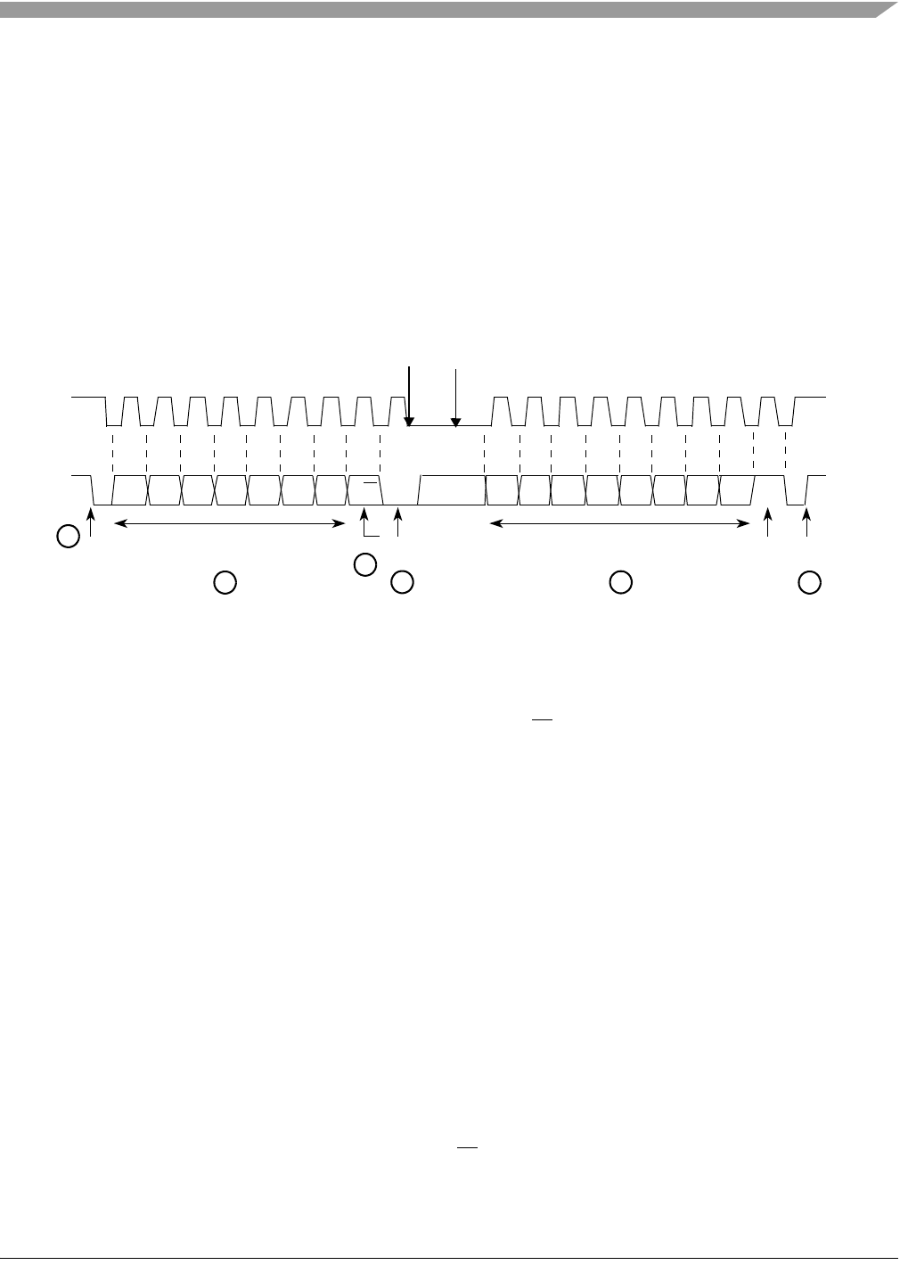
Functional Description
MCF548x Reference Manual, Rev. 3
Freescale Semiconductor 28-9
Normally, a standard communication is composed of four parts: START signal, slave address transmission,
data transfer, and STOP signal. The parts of a communication are described briefly in the following
sections and illustrated in Figure 28-8.
28.4.1 START Signal
When the bus is free—that is, when no master device is engaging the bus (both SCL and SDA lines are at
logical high)—a master may initiate communication by sending a START signal. A START signal (A in
Figure 28-8) is defined as a high-to-low transition of SDA while SCL is high. This signal denotes the
beginning of a new data transfer (each data transfer may contain several bytes of data) and awakens all
slaves.
Figure 28-8. Start, Address Transfer, and Stop Signal
28.4.2 Slave Address Transmission
The master sends the slave address in the first byte after the START signal (B in Figure 28-8). After the
seven-bit calling address (the slave address), it sends the R/W bit (C), which indicates the slave data
transfer direction (0 = write transfer; 1 = read transfer).
Each slave must have a unique address. An I2C master must not transmit its own slave address; it cannot
be master and slave at the same time.
The slave whose address matches that sent by the master pulls SDA low at the ninth serial clock (D) to
return an acknowledge bit.
28.4.3 STOP Signal
The master can terminate the communication by generating a STOP signal (“F” in Figure 28-8) to free the
bus. A STOP signal is defined as a low-to-high transition of SDA while SCL is at logical 1. The master
can generate a STOP even if the slave has generated an acknowledge, at which point the slave must release
the bus. The master may also generate a START signal followed by a calling command without generating
a STOP signal first. This is called repeated START. Refer to Section 28.4.6, “Repeated Start.”
28.4.4 Data Transfer
When successful slave addressing is achieved, the data transfer can proceed (E in Figure 28-8) on a
byte-by-byte basis in the direction specified by the R/W bit sent by the calling master. Each data byte is 8
bits long.
12345678 123456789 9
AD7 AD6 AD5 AD4 AD3 AD2 AD1 R/W XXX D7D6D5 D4D3D2D1D0
Slave (or Calling) Address R/W ACK
Bit
Data Byte No
ACK
Bit
STOP
Signal
lsbmsblsbmsb
SDA
SCL
START
Signal
A
BD
C
EF
SCL held low while
Interrupt is serviced
Interrupt bit is set
(Byte complete)
(Master driven) (Master driven)
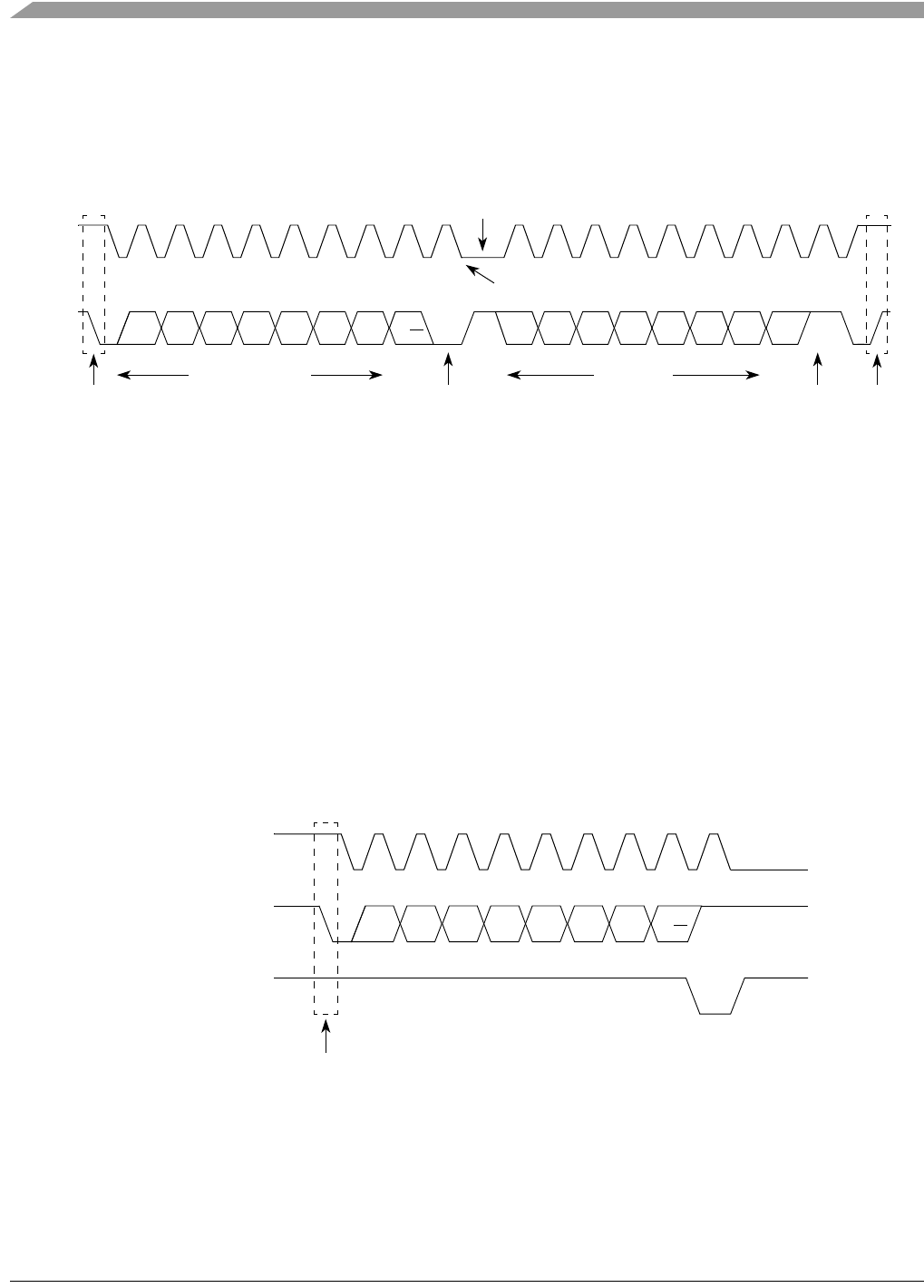
MCF548x Reference Manual, Rev. 3
28-10 Freescale Semiconductor
Data can be changed only while SCL is low and must be held stable while SCL is high, as Figure 28-8
shows. SCL is pulsed once for each data bit, with the msb being sent first. The receiving device must
acknowledge each byte by pulling SDA low at the ninth clock; therefore, a data byte transfer takes nine
clock pulses. (See Figure 28-9).
Figure 28-9. Data Transfer
28.4.5 Acknowledge
The transmitter releases the SDA line high during the acknowledge clock pulse as shown in Figure 28-10.
The receiver pulls down the SDA line during the acknowledge clock pulse so that it remains stable low
during the high period of the clock pulse.
If a slave-receiver does not acknowledge the byte transfer, the SDA must be left high by the slave. The
master then can generate a STOP condition to abort the transfer or generate a START signal (repeated start,
shown in Figure 28-8 and Figure 28-11, and discussed in Section 28.4.6, “Repeated Start) to start a new
calling sequence.
If a master-receiver does not acknowledge the slave transmitter after a byte transmission, it means end of
data to the slave, so the slave releases the SDA line for the master to generate a STOP or a START signal
(Figure 28-10).
Figure 28-10. Acknowledgement by Receiver
12345678956789
SCL 4321
Bit6 Bit4 Bit3 Bit2 Bit1Bit5SDA Bit7 Bit0 Bit6 Bit4 Bit3 Bit2 Bit1Bit5 Bit0Bit7
START
Signal
ACK from
Receiver
STOPNo
ACK
Bit
Data Byte
Slave Address
R/W
Signal
Interrupt Bit Set
(Byte Complete)
SCL Held Low while
Interrupt is Serviced
56789
SCL 4321
Bit6 Bit4 Bit3 Bit2 Bit1Bit5SDA by Transmitter Bit7 Bit0
START Signal
R/W
SDA by Receiver

Functional Description
MCF548x Reference Manual, Rev. 3
Freescale Semiconductor 28-11
28.4.6 Repeated Start
A repeated START signal is a START signal generated without first generating a STOP signal to terminate
the communication. This is used by the master to communicate with another slave or with the same slave
in a different mode without releasing the bus.
Various combinations of read/write formats are then possible:
• The first example in Figure 28-11 is the case of a master-transmitter transmitting to a
slave-receiver. The transfer direction is not changed.
• The second example in Figure 28-11 is the master reading slave data immediately after the first
byte. At the moment of the first acknowledge, the master-transmitter becomes a master-receiver
and the slave-receiver becomes a slave-transmitter.
• In the third example in Figure 28-11, the START condition and slave address are both repeated
using the repeated START signal. This is to communicate with the same slave in a different mode
without releasing the bus. The master transmits data to the slave first, and then the master reads
data from the slave by reversing the R/W bit.
Figure 28-11. Data Transfer, Combined Format
28.4.7 Clock Synchronization and Arbitration
I2C is a true multi-master bus that allows more than one master to be connected to it. If two or more masters
try to control the bus at the same time, a clock synchronization procedure determines the bus clock.
Because wire-AND logic is performed on the SCL line, a high-to-low transition on the SCL line affects all
the devices connected on the bus. The devices start counting their low period. Once a device’s clock has
gone low, it holds the SCL line low until the clock high state is reached. However, the change of low to
high in this device clock may not change the state of the SCL line if another device clock is still within its
low period. Therefore, synchronized clock SCL is held low by the device with the longest low period.
ST A
7-bit Slave Address 0A
DATA DATA A/A
R/W
SP
From Master to Slave
From Slave to Master
ST = Start
SP = Stop
A = Acknowledge (SDA low)
A = Not Acknowledge (SDA high)
ST A
7-bit Slave Address 1A
DATA DATA A
R/W
SP
ST A
1A
DATA
R/W
Rept A
7-bit Slave 0A
DATA DATA A/A
R/
W
SP
Rept ST = Repeated Start
ST Address
7-bit Slave
Address
Example 1:
Example 2:
Example 3:
Master Reads from Slave Master Writes to Slave
Note: No acknowledge on the last byte.
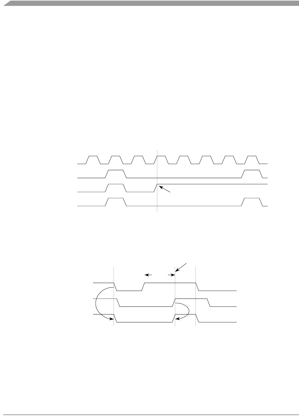
MCF548x Reference Manual, Rev. 3
28-12 Freescale Semiconductor
Devices with shorter low periods enter a high wait state during this time (see Figure 28-13). When all
devices concerned have counted off their low period, the synchronized clock SCL line is released and
pulled high. There is then no difference between the device clocks and the state of the SCL line and all the
devices start counting their high periods. The first device to complete its high period pulls the SCL line
low again.
The relative priority of the contending masters is determined by a data arbitration procedure. A bus master
loses arbitration if it transmits logic "1" while another master transmits logic "0". The losing masters
immediately switch over to slave receive mode and stop driving SDA output (see Figure 28-12). In this
case the transition from master to slave mode does not generate a STOP condition. Meanwhile, hardware
sets I2SR[IAL] to indicate loss of arbitration.
28.4.8 Handshaking and Clock Stretching
The clock synchronization mechanism can be used as a handshake in data transfers. Slave devices may
hold the SCL low after completion of one byte transfer, which will cause the bus clock to halt, forcing the
master clock into wait status until the slave releases the SCL line.
Figure 28-12. Arbitration Procedure
Slaves may also slow down the bit rate transfer. After the master has driven SCL low, the slave can drive
SCL low for the required period and then release it. If the slave SCL low period is greater than the master
SCL low period, then the resulting SCL bus signal low period is stretched.
Figure 28-13. Clock Synchronization
28.5 Initialization Sequence
Reset will put the I2C control register in its default status. Before the interface can be used to transfer serial
data, an initialization procedure must be carried out, as follows:
1. Update I2FDR[IC] to select the required division ratio to obtain the SCL frequency from the
system clock
SCL
SDA by Master1
SDA by Master2
SDA
Master2 Loses Arbitration, and
becomes Slave-Receiver
SCL by Master2
SCL by Master1
SCL
Start Counting High Period
Wait
State

Initialization Sequence
MCF548x Reference Manual, Rev. 3
Freescale Semiconductor 28-13
2. Update the I2ADR to define it as a slave device (give it a slave address)
3. Set I2CR[IEN] to enable the I2C interface system
4. Modify the I2CR to select master/slave mode, transmit/receive mode, or interrupt enable
NOTE
If I2SR[IBB] is set when the I2C bus module is enabled, execute the
following code sequence before proceeding with normal initialization code.
This issues a STOP command to the slave device, placing it in an idle state
as if it were just power-cycled on.
I2ICR = 0x00
I2CR = 0x0
I2CR = 0xA
dummy read of I2DR
I2SR = 0x0
I2CR = 0x0
I2ICR = 0x01
28.5.1 Transfer Initiation and Interrupt
After completing initialization, serial data can be transmitted by selecting master transmit mode. If the
device is connected to a multi-master bus system, the state of the bus busy bit (BB) must be tested to check
whether the serial bus is free.
If the bus is free (BB = 0), the first byte (the slave address) can be sent. The data written to the data register
comprises the slave calling address, and the LSB is set to indicate the direction of transfer required from
the slave.
Depending on the relative frequencies of the system clock and the SCL period, it may be necessary to wait
until the bus is busy after writing the calling address to the data register (I2DR) before proceeding with the
following instructions.
Following is an example of how to generate a START signal:
/**********************************
* START generation in Master mode *
***********************************/
/* Make sure bus is idle (poll Bus Busy bit) */
while ( (MCF_I2C_I2SR & MCF_I2C_I2SR_IBB) );
/* Put module in master TX mode (generates START) */
MCF_I2C_I2CR |= 0x10;
MCF_I2C_I2CR |= 0x20;
/* Put target address into I2DR */
MCF_I2C_I2DR = TARGET_ADDR;

MCF548x Reference Manual, Rev. 3
28-14 Freescale Semiconductor
/* Wait for I2SR.IBB (bus busy) to be set */
while ( !(MCF5_I2C_I2SR & MCF_I2C_I2SR_BB) );
28.5.2 Post-Transfer Software Response
Transmission or reception of a byte will set the data transferring bit (ICF) to 1, which indicates one byte
of communication is finished. The interrupt bit (IIF) is set also; an interrupt will be generated if the
interrupt function was enabled during initialization (by setting the IEN bit). Software must clear the IIF bit
in the interrupt service routine first. The ICF bit will be cleared automatically by reading from the data I/O
register (I2DR) in receive mode or writing to I2DR in transmit mode.
Software may service the bus I/O in the main program by monitoring the IIF bit if the interrupt function is
disabled. Note that polling should monitor the IIF bit rather than the ICF bit, because their operation is
different when arbitration is lost.
Also note that when an interrupt occurs at the end of the address cycle, the master will always be in
transmit mode, i.e. the address is transmitted. If master receive mode is required, indicated by the R/W bit
in I2DR, then the MTX bit should be toggled at this stage.
During slave mode address cycles (AAS = 1), the SRW bit in the status register is read to determine the
direction of the subsequent transfer, and the MTX bit is programmed accordingly. For slave mode data
cycles (AAS = 0) the SRW bit is not valid; therefore, the MTX bit in the control register should be read to
determine the direction of the current transfer.
Following is an example of how to monitor IIF instead of ICF:
/*********************************************
* Master TX with interrupt function disabled *
**********************************************/
/* Send the contents of tx_buffer */
for (i=0; i<tx_byte_count; i++)
{
/* Put data to be sent into I2DR */
MCF_I2C_I2DR = tx_buffer[i];
/*Wait for transfer to complete (Poll IIF bit) */
while (!(MCF_I2C_I2SR & MCF_I2C_I2SR_IIF) );
/* Clear IIF bit */
MCF_I2C_I2SR &= 0xFD;
}

Initialization Sequence
MCF548x Reference Manual, Rev. 3
Freescale Semiconductor 28-15
28.5.3 Generation of STOP
A data transfer ends with a STOP signal generated by the ‘master’ device. A master transmitter can simply
generate a STOP signal after all the data has been transmitted.
For a master receiver to terminate a data transfer, it must inform the slave transmitter by not
acknowledging the last byte of data. The informing of the slave transmitter is done by two operations:
• Before reading the second to the last byte of data, the master receiver must set the transmit
acknowledge bit (TXAK).
• Before reading the last byte of data, the master receiver must write a zero to the master/slave mode
select bit (MSTA). This will generate the STOP signal.
The I2C interrupt bit (IIF) in the status register is set when an interrupt is pending, which will cause a
processor interrupt request if the interrupt enable bit (IIEN) in the control register is set. The IIF bit is set
when one of the following events occurs:
1. Complete one byte transfer (set at the falling edge of the ninth clock).
2. Receive a calling address that matches its own specific address in slave receive mode.
3. Arbitration is lost.
Following is an example that shows a master RX where NACK occurs and STOP is generated.
/*********************************************
* Master RX with interrupt function disabled *
**********************************************/
/* Receive data from slave and store in rx_buffer */
for (i=0; i<rx_byte_count; i++)
{
/* Wait for transfer to complete */
while (!(MCF_I2C_I2SR & MCF_I2C_I2SR_IIF) );
/* Clear IIF bit */
MCF_I2C_I2SR &= 0xFD;
/* Check for second-to-last and last byte transmission. After second-to-last byte is
received, the ACK bit must be disabled in order to signal the slave that the last byte
has been received. The actual NACK does not take place until after the last byte has been
received. */
if (i==(rx_byte_count-2))
{
/*Disable Acknowledge (set I2CR.TXAK) */
MCF_I2C_I2CR |= MCF_I2C_I2CR_TXAK;
}
if (i==(rx_byte_count-1))
{

MCF548x Reference Manual, Rev. 3
28-16 Freescale Semiconductor
/* Generate STOP by clearing I2CR.MSTA */
MCF_I2C_I2CR = 0x80;
}
/*Store received data and release SDA */
rx_buffer[i] = MCF_I2C_I2DR;
}
28.5.4 Generation of Repeated START
At the end of a data transfer, if the master still wants to communicate on the bus, it can generate another
START signal followed by another slave address without first generating a STOP signal. This is done by
writing a 1 to I2CR[MSTA].
28.5.5 Slave Mode
In the slave interrupt service routine, the addressed as slave bit (IAAS) should be tested to check if a calling
of its own address has just been received. If IAAS is set, software should set the transmit/receive mode
select bit (I2CR[MTX]) according to the R/W command bit (SRW). Writing to the control register clears
the IAAS automatically.
NOTE
Note that the only time IAAS is read as set is from the interrupt at the end
of the address cycle where an address match occurred; interrupts resulting
from subsequent data transfers will have IAAS cleared.
A data transfer may now be initiated by writing information to the data register, for slave transmits, or
dummy reading an address from the data register, in slave receive mode. The slave will drive SCL low in
between byte transfers; SCL is released when the data register is accessed in the required mode.
If the slave data register is not read after a transfer, the slave module will hold the SDA line low
indefinitely. The master is able to send a stop signal in this situation, but the slave does not respond by
releasing the SDA line. This functionality is a by-product of the arbitration scheme. To avoid this problem,
the slave data register must be read before a stop signal is issued.
In a slave transmitter routine, the received acknowledge bit (RXAK) must be tested before transmitting
the next byte of data. A dummy read of the last transmitted byte then releases the SCL line so that the
master can generate a STOP signal.
NOTE
Setting RXAK means an “end of data” signal from the master receiver, after
which the slave must be switched from transmitter mode to receiver mode
by software.
Following are examples of slave TX and RX illustrating the dummy read of I2DR and, for slave TX, the
checking of RXAK:
/************************************************************************
* Slave TX illustrating NACK on last byte (interrupt function disabled) *
*************************************************************************/

Initialization Sequence
MCF548x Reference Manual, Rev. 3
Freescale Semiconductor 28-17
/* Set I2CR.MTX to put the module in transit mode */
MCF_I2C_I2CR |= MCF_I2C_I2CR_MTX;
/* Send the contents of tx_buffer until NACK is detected */
i = 0;
while (1)
{
/*Put TX data into I2DR */
MCF_I2C_I2DR = tx_buffer[i];
/*Wait for transfer to complete */
while (!(MCF_I2C_I2SR & MCF_I2C_I2SR_IIF) );
/* Clear IIF bit */
MCF_I2C_I2SR &= 0xFD;
/*Detect when no ACK is received */
if(MCF_I2C_I2SR & MCF_I2C_I2SR_RXAK)
{
/*Finish the transfer by putting the module into its idle state. */
MCF_I2C_I2CR = 0x80;
break;
}
i++;
}
/*************************************************************************
* Slave RX illustrating dummy read of I2DR (interrupt function disabled) *
**************************************************************************/
/* Clear I2CR.MTX to put the module in receive mode */
MCF_I2C_I2CR &= 0xEF;
/* Dummy read of I2DR to signal the module is ready for the next byte */
dummy_read = MCF_I2C_I2DR;

MCF548x Reference Manual, Rev. 3
28-18 Freescale Semiconductor
/* Receive data from master device and store in rx-buffer */
for(i=0; i<rx_byte_count; i++)
{
/* Wait for transfer to complete */
while (!(MCF_I2C_I2SR & MCF_I2C_I2SR_IIF) );
/* Clear IIF bit */
MCF_I2C_I2SR &= 0xFD;
/* Store received data and release SDA */
rx_buffer[i] = MCF_I2C_I2DR;
}
28.5.6 Arbitration Lost
If several masters try to engage the bus simultaneously, only one master wins and the others lose
arbitration. The devices which lost arbitration are immediately switched to slave receive mode by the
hardware. Their master that has lost arbitration immediately releases the bus, but SCL is still generated
until the end of the byte during which arbitration was lost. An interrupt occurs at the falling edge of the
ninth clock of this transfer with IAL = 1 and MSTA = 0.
If the MCF548x attempts to start transmission while the bus is being engaged by another master, the
hardware will inhibit the transmission, switch the MSTA bit from 1 to 0 without generating a STOP
condition, generate an interrupt to the CPU, and set the IAL bit to indicate that the attempt to engage the
bus has failed. When considering these cases, the slave service routine should test the IAL bit first, and the
software should clear the IAL bit if it is set.
28.5.7 Flow Control
Figure 28-14 displays the flow of a typical I2C interrupt process.
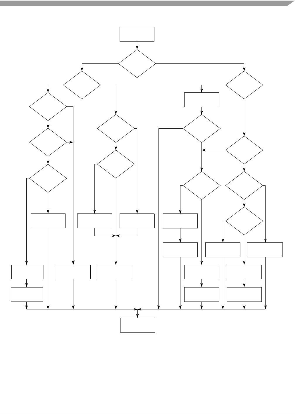
Initialization Sequence
MCF548x Reference Manual, Rev. 3
Freescale Semiconductor 28-19
Figure 28-14. Flow-Chart of Typical I2C Interrupt Routine
Clear IIF
Tx/Rx
?
Second
Last Byte to
be Read
?
Clear IAL
Last Byte
to be Read
?
Switch to
Rx Mode
Dummy Read
from I2DR
Set
TXAK=1 Generate
STOP Signal
Generate
STOP Signal
Read Data from
I2DR and Store
Set
Tx Mode
Write Data
to I2DR Tx Next
Byte
Read Data from
I2DR and Store
Set
Rx Mode Switch to
Rx Mode
Dummy Read
from I2DR Dummy Read
from I2DR
RTE
Arbitration
Lost
?
IAAS=1
?
IAAS=1
?
SRW=1
?Tx/Rx
?
ACK from
Receiver
?
Ye s
No
Yes
Tx
Rx
No
Ye s
No
(Write)
(Read)
Ye s
No
Tx Rx
Yes
No
Yes
No
No
Ye s
Data
Cycle
Address
Cycle
No
Ye s
No
Yes
Last Byte
Transmitted
?
RXAK=0
?
End of
Addr Cycle
(Master Rx)
?
Write Next
Byte to I2DR
No
Yes
Yes
No
Master
Mode
?

MCF548x Reference Manual, Rev. 3
28-20 Freescale Semiconductor

MCF548x Reference Manual, Rev. 3
Freescale Semiconductor 29-1
Chapter 29
USB 2.0 Device Controller
29.1 Introduction
This chapter provides an overview of the USB 2.0 device controller module of the xMCF548x. Connection
examples and circuit board layout considerations are also provided.
The USB Specification, Revision 2.0 is a recommended supplement to this chapter. It can be downloaded
from http://www.usb.org. Chapter 2 of this specification, Terms and Abbreviations, provides definitions of
many of the terms found here.
29.1.1 Overview
The Universal Serial Bus specification describes three types of devices that can connect to the bus. The
USB host is the bus master, and periodically polls peripherals to initiate data transfers. There is only one
host on the bus. The USB function (or USB device) is a bus slave. It can communicate only with a USB
host. It does not generate bus traffic and only responds to requests from the host. A USB hub is a special
class of USB function that adds additional connection points to the bus for more USB devices.
The integrated USB 2.0 device controller of the xMCF548x implements most of the USB protocol in
hardware, hiding all direct interaction with the USB. The memory mapped registers allow the user to
enable or disable the USB module, control characteristics of the individual endpoints, and monitor traffic
flow through the module without having to manage the low-level details of the USB protocol. A set of
intelligent FIFOs are implemented that allow for easy data management via the ColdFire core or the
multichannel DMA.
While this module hides all direct interaction with the protocol, knowledge of the USB is required in order
to properly configure the device for operation on the bus. Programming requirements are covered in this
chapter, with additional information in the USB Specification, Revision 2.0.
29.1.2 Features
The xMCF548x USB 2.0 device controller provides the following features:
• Compliant with the USB Specification, Revision 2.0
• Supports high-speed (480 Mbps) and full-speed (12 Mbps) devices
• One control endpoint and 6 endpoints programmable as interrupt, bulk, or isochronous
• Fully automatic processing of the SET_FEATURE, CLEAR_FEATURE,
GET_CONFIGURATION, GET_INTERFACE, GET_STATUS, and SET_ADDRESS USB
standard device requests
• Processing with application intervention of the SET_CONFIGURATION, SET_INTERFACE,
SET_DESCRIPTOR, GET_DESCRIPTOR, and non-standard USB device requests
• Administration for up to 7 endpoints, 32 configurations, 32 interfaces, and 32 alternate settings
• Support for remote wakeup
• ColdFire core and multichannel DMA access to the intelligent FIFOs that handle all packet retries
and data framing
• Internal USB 2.0 physical layer transceiver
• 4 KByte of FIFO RAM and 1 KByte of descriptor RAM
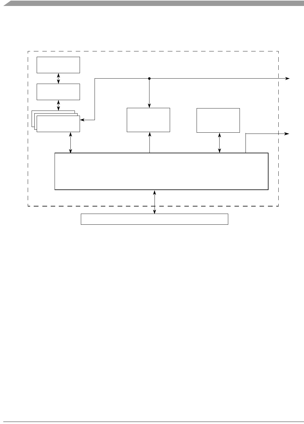
MCF548x Reference Manual, Rev. 3
29-2 Freescale Semiconductor
29.1.3 Block Diagram
A block diagram of the complete USB 2.0 Device controller module is shown in Figure 29-1.
Figure 29-1. USB 2.0 Device Controller Block Diagram
29.1.3.1 Controller and Synchronization
This block handles all of the details of managing the USB protocol and presents a simple set of handshakes
to the application for managing data flow, vendor commands, and configuration information.
The control logic portion of the module implements the control logic and registers that allow the user to
control and communicate with the USB module. The registers are described in Section 29.2.1, “USB
Memory Map.”
The register functions include interrupt status/mask, USB descriptor download, FIFO control and access,
and processing of GET_DESCRIPTOR device requests from control endpoints.
The device core operates on a fixed 30-MHz clock that is generated inside the USB 2.0 physical layer
transceiver (PHY). All other non-core logic runs at the CommBus frequency. The synchronization block
synchronizes the signals that cross between these two clock domains.
29.1.3.2 Descriptor RAM
The descriptor RAM is used to preload the descriptor tables and modify them as necessary. The USB
module can handle the data movement out of this RAM for a USB GET_DESCRIPTOR SETUP
transaction based on the information programmed into the DRAMDR. This operation is described in
Section 29.4.1.1, “USB Descriptor Download”.
FIFO RAM
FIFO RAM
Manager
FIFO Control Arbiter Descriptor
RAM
Integrated USB 2.0 PHY
Comm Bus
USB Controller and Synchronization Logic
Interrupt
USB 2.0 Device Controller

Introduction
MCF548x Reference Manual, Rev. 3
Freescale Semiconductor 29-3
29.1.3.3 FIFO Controller
The FIFO controller implements the data FIFOs in such a way that they can communicate with the
ColdFire core or with the multichannel DMA. There are two physical RAMs that are shared by all of the
FIFO controllers. For maximum performance, the two RAMs can be configured such that one stores
transmit (IN) endpoint data and the other stores receive (OUT) endpoint data. If maximum RAM allocation
flexibility is more important than maximum performance, the RAMs can be configured such that the entire
space is shared by all IN/OUT endpoints. User programmable registers also allow on-the-fly configuration
of individual FIFO sizes and direction.
In order to achieve maximum USB bandwidth, the USB device must be able to provide or receive full
packets of data to or from the USB host immediately upon request. In order to satisfy this requirement,
there is one FIFO for each USB endpoint. The actual FIFO size for each endpoint is programmable.
Typically, BULK and ISOCHRONOUS endpoint FIFOs should be twice the packet size. INTERRUPT and
CONTROL endpoint FIFOs should be programmed to the size of at least one packet.
29.1.3.4 FIFO RAM Manager
The FIFO RAM manager block consists of a memory configuration controller, a FIFO RAM multiplexor,
and a memory request arbitrator. Together, these three functional units allow one or more FIFO modules
to share access to the FIFO memory. While the memory is physically configured as two independent
dual-port SRAM modules, the RAM manager is responsible for partitioning it into individual blocks for
each FIFO controller, and managing the addressing to allow byte, word, or longword access from any byte
offset.
The memory configuration controller partitions the RAM into a set of user specified blocks.
The memory multiplexor and the arbitrator work together to ensure that the correct FIFO has access to the
RAM, and that simultaneous requests to the RAM’s ports are fairly arbitrated.
See the USBCR[RAMSPLIT] bit description and the EPnFRCFGR description for more information on
programming the settings for these blocks.
29.1.3.5 Integrated USB 2.0 Transceiver
The USB 2.0 Device Controller module includes an internal full and high-speed physical layer transceiver
(PHY). The bus interface signals are described below.
29.1.3.5.1 USB Differential Data (USBD+, USBD–)
USBD+ and USBD– are the outputs of the on-chip USB 2.0 physical layer transceiver. They provide
differential data for the USB 2.0 bus.
29.1.3.5.2 USBVBUS
USB cable Vbus monitor input.
29.1.3.5.3 USBRBIAS
Connection for external current setting resistor. This signal should be connected to a 9.1 KΩ +/– 1%
pull-down resistor.

MCF548x Reference Manual, Rev. 3
29-4 Freescale Semiconductor
29.1.3.5.4 USBCLKIN
Input pin for the 12-MHz USB crystal circuit.
29.1.3.5.5 USBCLKOUT
Output pin for the 12-MHz USB crystal circuit.
29.2 Memory Map/Register Definition
This section contains a detailed description of each register and its specific function.
29.2.1 USB Memory Map
Table 29-1 contains a memory map for all the USB 2.0 Device Controller registers.
NOTE
Registers should only be accessed using their full size. For example, a 32-bit
register should be read as one longword instead of two words or four bytes.
Table 29-1. USB Memory Map
Address
(MBAR +) Name Byte0 Byte1 Byte2 Byte3
USB Request, Control, and Status Registers
0xB000 Application interrupt status register,
Application interrupt mask register,
Reserved
Endpoint info register
USBAISR USBAIMR — EPINFO
0xB004 Configuration value register,
Configuration attribute register,
Device speed register
Reserved
CFGR CFGAR SPEEDR —
0xB008 Reserved
0xB00C USB frame number register — FRMNUMR
0x8010 Endpoint transaction number register EPTNR —
0xB014 Application interface update register IFUR —
0xB018–
0xB03F
Reserved
0xB040–
0xB07C
Configuration interface registers 0–31 IFRnIFRn
USB Counter Registers
0xB080 USB packet passed count register,
USB dropped packet counter register
PPCNT DPCNT
0xB084 USB CCR error counter register,
USB bitstuffing error counter register
CRCECNT BSECNT

Memory Map/Register Definition
MCF548x Reference Manual, Rev. 3
Freescale Semiconductor 29-5
0xB088 USB PID error counter register,
USB framing error counter register
PIDECNT FRMECNT
0xB08C USB transmitted packet counter register
USB counter overflow register
Reserved
TXPCNT CNTOVR —
0xB090–
0xB0FF
Reserved
Endpoint Context Registers
0xB100 EP0 attribute control register,
EP0 max packet size register
— EP0ACR EP0MPSR
0xB104 EP0 interface number register,
EP0 status register,
bmRequest type register,
bRequest type register
EP0IFR EP0SR BMRTR BRTR
0xB108 wValue register,
wIndex register
WVALUER WINDEXR
0xB10C wLength register WLENGTHR —
0xB110–
0xB12F
Reserved
0xB130 EP1 OUT attribute control register,
EP1 OUT max packet size register
— EP1OUTAC
R
EP1OUTMPSR
0xB134 EP1 OUT interface number register,
EP1 OUT status register
EP1OUTIFR EP1OUTSR — —
0xB138 Reserved
0xB13C EP1 OUT sync frame register EP1OUTSFR
0xB140–
0xB147
Reserved
0xB148 EP1 IN attribute control register,
EP1 IN max packet size register
— EP1INACR EP1INMPSR
0xB14C EP1 IN interface number register,
EP1 IN status register
EP1INIFR EP1INSR — —
0xB150–
0xB154
Reserved
0xB158 EP1 IN sync frame register EP1INSFR
0xB15C–
0xB15F
Reserved
0xB160 EP2 OUT attribute control register,
EP2 OUT max packet size register
— EP2OUTAC
R
EP2OUTMPSR
Table 29-1. USB Memory Map (Continued)
Address
(MBAR +) Name Byte0 Byte1 Byte2 Byte3

MCF548x Reference Manual, Rev. 3
29-6 Freescale Semiconductor
0xB164 EP2 OUT interface number register,
EP2 OUT status register
EP2OUTIFR EP2OUTSR — —
0xB168 Reserved
0xB16C EP2 OUT Sync Frame Register EP2OUTSFR
0xB170–
0xB177
Reserved
0xB178 EP2 IN attribute control register,
EP2 IN max packet size register
— EP2INACR EP2INMPSR
0xB17C EP2 IN interface number register,
EP2 IN status register
EP2INIFR EP2INSR — —
0xB180–
0xB184
Reserved
0xB188 EP2 IN sync frame register EP2INSFR
0xB18C–
0xB18F
Reserved
0xB190 EP3 OUT attribute control register,
EP3 OUT max packet size register
– EP3OUTAC
R
EP3OUTMPSR
0xB194 EP3 OUT interface number register,
EP3 OUT status register
EP3OUTIFR EP3OUTSR — —
0xB198 Reserved
0xB19C EP3 OUT sync frame register EP3OUTSFR
0xB1A0–
0xB1A7
Reserved
0xB1A8 EP3 IN attribute control register,
EP3 IN max packet size register
– EP3INACR EP3INMPSR
0xB1AC EP3 IN interface number register,
EP3 IN status register
EP3INIFR EP3INSR — —
0xB1B0–
0xB1B7
Reserved
0xB1B8 EP3 IN sync frame register EP3INSFR
0xB1BC–
0xB1BF
Reserved
0xB1C0 EP4 OUT attribute control register,
EP4 OUT max packet size register
— EP4OUTAC
R
EP4OUTMPSR
0xB1C4 EP4 OUT interface number register,
EP4 OUT status register
EP4OUTIFR EP4OUTSR — —
0xB1C8 Reserved
0xB1CC EP4 OUT sync frame register EP4OUTSFR
Table 29-1. USB Memory Map (Continued)
Address
(MBAR +) Name Byte0 Byte1 Byte2 Byte3

Memory Map/Register Definition
MCF548x Reference Manual, Rev. 3
Freescale Semiconductor 29-7
0xB1D0–
0xB1D7
Reserved
0xB1D8 EP4 IN attribute control register,
EP4 IN max packet size register
— EP4INACR EP4INMPSR
0xB1DC EP4 IN interface number register, EP4 IN
status register
EP4INIFR EP4INSR — —
0xB1E0–
0xB1E7
Reserved
0xB1E8 EP4 IN sync frame register EP4INSFR
0xB1EC–
0xB1EF
Reserved
0xB1F0 EP5 OUT attribute control register, EP5
OUT max packet size register
— EP5OUTAC
R
EP5OUTMPSR
0xB1F4 EP5 OUT interface number register, EP5
OUT status register
EP5OUTIFR EP5OUTSR — —
0xB1F8 Reserved
0xB1FC EP5 OUT sync frame register EP5OUTSFR
0xB200–
0xB207
Reserved
0xB208 EP5 IN attribute control register,
EP5 IN max packet size register
— EP5INACR EP5INMPSR
0xB20C EP5 IN interface number register,
EP5 IN status register
EP5INIFR EP5INSR — —
0xB210–
0xB214
Reserved
0xB218 EP5 IN sync frame register EP5INSFR
0xB21C–
0xB21F
Reserved
0xB220 EP6 OUT attribute control register, EP6
OUT max packet size register
— EP6OUTAC
R
EP6OUTMPSR
0xB224 EP6 OUT interface number register, EP6
OUT status register
EP6OUTIFR EP6OUTSR — —
0xB228 Reserved
0xB22C EP6 OUT sync frame register EP6OUTSFR
0xB230–
0xB237
Reserved
0xB238 EP6 IN attribute control register,
EP6 IN max packet size register
— EP6INACR EP6INMPSR
Table 29-1. USB Memory Map (Continued)
Address
(MBAR +) Name Byte0 Byte1 Byte2 Byte3

MCF548x Reference Manual, Rev. 3
29-8 Freescale Semiconductor
0xB23C EP6 IN interface number register, EP6 IN
status register
EP6INIFR EP6INSR — —
0xB240–
0xB244
Reserved
0xB248 EP6 IN sync frame register EP6INSFR
0xB24C–
0xB3FF
Reserved
USB Request, Control, and Status Registers
0xB400 USB status register USBSR
0xB404 USB control register USBCR
0xB408 USB descriptor RAM control register DRAMCR
0xB40C USB descriptor RAM data register DRAMDR
0xB410 USB interrupt status register USBISR
0xB414 USB interrupt mask register USBIMR
0xB418–
0xB43F
Reserved
USB Endpoint FIFO Registers
0xB440 EP0 status and control register EP0STAT
0xB444 EP0 interrupt status register EP0ISR
0xB448 EP0 interrupt mask register EP0IMR
0xB44C EP0 FIFO RAM configuration register EP0FRCFGR
0xB450 EP0 FIFO data register EP0FDR
0xB454 EP0 FIFO status register EP0FSR
0xB458 EP0 FIFO control register EP0FCR
0xB45C EP0 FIFO alarm register EP0FAR
0xB460 EP0 FIFO read pointer EP0FRP
0xB464 EP0 FIFO write pointer EP0FWP
0xB468 EP0 last read frame pointer EP0LRFP
0xB46C EP0 last write frame pointer EP0LWFP
0xB470–
0xB49F
EP1 FIFO registers
0xB4A0–
0xB4CF
EP2 FIFO registers
Table 29-1. USB Memory Map (Continued)
Address
(MBAR +) Name Byte0 Byte1 Byte2 Byte3

Memory Map/Register Definition
MCF548x Reference Manual, Rev. 3
Freescale Semiconductor 29-9
29.2.2 USB Request, Control, and Status Registers
The following registers provide an application interface to the request, control, and status functionality of
the USB 2.0 device controller.
29.2.2.1 USB Status Register (USBSR)
The USBSR reports the current state of various features of the module. This register is read only.
0xB4D0–
0xB4FF
EP3 FIFO registers
0xB500–
0xB52F
EP4 FIFO registers
0xB530–
0xB55F
EP5 FIFO registers
0xB560–
0xB58F
EP6 FIFO registers
31 30 29 28 27 26 25 24 23 22 21 20 19 18 17 16
R Uninitialized
W
Reset Uninitialized
1514131211109876543210
R Uninitialized SUSP Uninitialized ISOERREP
W
Reset Uninitialized 0 Uninitialized 0 0 0 0
Reg
Addr
MBAR + 0xB400
Figure 29-2. USB Status Register (USBSR)
Table 29-2. USBSR Field Descriptions
Bits Name Description
31–8 — Reserved, should be cleared.
7 SUSP Suspend. This is the USB suspend indicator.
0 USB is not suspended.
1 USB is suspended.
Table 29-1. USB Memory Map (Continued)
Address
(MBAR +) Name Byte0 Byte1 Byte2 Byte3

MCF548x Reference Manual, Rev. 3
29-10 Freescale Semiconductor
29.2.2.2 USB Control Register (USBCR)
The USBCR configures features of the module.
6–4 — Reserved, should be cleared.
3–0 ISOERREP Isochronous error endpoint. This is the endpoint number for the isochronous OUT endpoint
that has experienced a PID sequencing error and caused the ISO_ERR interrupt to assert.
The value in this register will always reflect the endpoint number for the last isochronous
OUT endpoint to experience a PID sequencing error (or 0x0 if no PID sequencing errors
have occurred). It is not cleared along with the USBISR[ISOERR] interrupt bit.
31 30 29 28 27 26 25 24 23 22 21 20 19 18 17 16
R Uninitialized
W
Reset Uninitialized
15 14 13 12 11 10 9 8 7 6 5 4 3 2 1 0
R Uninitialized RAM
SPLIT
—RAM
EN
0APP
LOCK
0
WRST RESUME
Reset Uninitialized 0000000 0
Reg
Addr
MBAR + 0xB404
Figure 29-3. USB Control Register (USBCR)
Table 29-2. USBSR Field Descriptions
Bits Name Description

Memory Map/Register Definition
MCF548x Reference Manual, Rev. 3
Freescale Semiconductor 29-11
Table 29-3. USBCR Field Descriptions
Bits Name Description
31–6 — Reserved, should be cleared.
5 RAMSPLIT RAM split. The endpoint FIFO RAM can be configured for maximum flexibility or for maximum
performance. The individual FIFO base and depth values (in the EPnFRCFGR) should be carefully
programmed taking into account the respective direction (IN/OUT) of each FIFO and the value of this
control register. Care should be taken not to program those values such that the space required
exceeds the FIFO space available to the IN/OUT endpoints.
Setting this bit configures the endpoint FIFO RAM for maximum performance by splitting the total
endpoint FIFO RAM space in half, dedicating half to be shared by all IN endpoints and the other half
to be shared by all OUT endpoints. In this configuration, both the USB module and the
application/DMA can receive/transmit the endpoint FIFO data without incurring wait states due to
FIFO RAM arbitration.
If set, special care must be taken with the bi-directional control endpoint, endpoint 0. In this case,
software must configure space in both the Rx and Tx RAM regions for the control EP since it is
bi-directional depending on the request type. Furthermore, if the seperate regions within the Rx and
Tx RAM spaces do not have the same base address and byte depth for EP0, the software must be
sure to set the EP0FRCFGR[BASE] and EP0FRCFGR[DEPTH] values appropriately before
servicing a Control read/write request.
Clearing this bit configures the endpoint FIFO RAM for maximum flexibility at the cost of
performance. In this configuration, the entire endpoint FIFO RAM space can be shared by all
endpoints. However, application/DMA accesses will incur wait states when accessing the endpoint
FIFO data at the same time that the USB is receiving/transmitting data.
0 The endpoint FIFO RAM is configured for maximum flexibility.
1 The endpoint FIFO RAM is configured for maximum performance.
4 — Reserved, should be cleared.
3 RAMEN Descriptor RAM Enable. This bit determines the accessibility of the descriptor RAM contents.
0 The application can read/write the descriptor RAM via the DRAMDR register. The device cannot
access the descriptor RAM contents.
1 The USB device controller can read the descriptor RAM as controlled by the DRAMCR register.
The user cannot access the descriptor RAM contents.
2 RST USB reset. This bit executes a hard reset of the USB module. This bit allows the system software to
force a reset of the USB’s logic when the system is first connected to the USB, or for debug
purposes.

MCF548x Reference Manual, Rev. 3
29-12 Freescale Semiconductor
29.2.2.3 USB Descriptor RAM Control Register (DRAMCR)
1 APPLOCK Application Lock. This bit should be asserted to ensure the indivisibility of read-modify-write (RMW)
operations on certain USB 2.0 device registers. Many register bits can be written to by the user
software and the internal logic. Collisions between these two agents can occur when the user
software is performing a RMW operation on any of these register bits while the internal logic tries to
update the same bit(s) between the read cycle and the write cycle of the user software. For RMW
operations, the user software should set this bit before the read and clear it after the completion of
the write.
The register bits that require this "locked" RMW operation are:
USBAISR[7:0]
EPnOUTSR/EPnINSR[5]
EPnOUTSR/EPnINSR[3:2]
EPnOUTSR/EPnINSR[0]
CFGAR[6]
0 APPLOCK is deasserted.
1 APPLOCK is asserted.
0 RESUME Resume. This initiates resume signalling on the USB. If remote wake-up capability is enabled for the
current USB configuration, writing a 1 to this bit will cause the USB module to initiate resume
signalling on the bus. This bit automatically resets to 0 after a write. Writing a 0 to this bit has no
effect. If remote wake-up capability has been disabled in the USB via the CLEAR_FEATURE
request, then this bit will have no effect. Any user software should have a time-out feature that aborts
the remote wake-up attempt after some time if the RESUME interrupt does not occur.
31 30 29 28 27 26 25 24 23 22 21 20 19 18 17 16
R0 BSY Uninitialized DSIZE
WSTART
Reset0 0 Uninitialized 00000000000
15 14131211109876543210
R Uninitialized DADR
W
Reset Uninitialized 0000000000
Reg
Addr
MBAR + 0xB408
Figure 29-4. USB Descriptor RAM Control Register (DRAMCR)
Table 29-3. USBCR Field Descriptions (Continued)
Bits Name Description

Memory Map/Register Definition
MCF548x Reference Manual, Rev. 3
Freescale Semiconductor 29-13
29.2.2.4 USB Descriptor RAM Data Register (DRAMDR)
The DRAMDR allows user access to the USB descriptor memory.
Table 29-4. DRAMCR Field Descriptions
Bits Name Description
31 START Start. This bit initiates the GET_DESCRIPTOR handler. Before setting this bit, the software must
set the DSIZE[10:0] and DADR[9:0] values to the appropriate values for the current
GET_DESCRIPTOR request. This bit automatically resets to 0 after a write. Writing a 0 to this bit
has no effect.
30 BSY Busy. This read only bit is the GET_DESCRIPTOR handler busy signal.
0 The GET_DESCRIPTOR handler is idle.
1 The GET_DESCRIPTOR handler is busy sending the specified descriptor to the USB.
29–27 — Reserved, should be cleared.
26–16 DSIZE Descriptor size. This is the descriptor size. When the GET_DESCRIPTOR handler is initiated, this
value should be set to the length of the requested descriptor within the descriptor RAM.
15–10 — Reserved, should be cleared.
9–0 DADR Descriptor address. This is the descriptor offset in bytes from the RAM base address. This register
allows user access to the USB descriptor RAM and is also used by the GET_DESCRIPTOR handler
when servicing GET_DESCRIPTOR requests.
For user access: The user programs a desired address into the DADR[9:0] bits, then follows it with
a read or write to the DRAMDR register to complete the access. Upon read/write access to
DRAMDR, the address in DADR will increment automatically.
For GET_DESCRIPTOR handler access: When the GET_DESCRIPTOR handler is initiated, this
value should be set to the address within the descriptor RAM of the first byte of the requested
descriptor. The descriptor RAM is 1024 bytes deep.
31 30 29 28 27 26 25 24 23 22 21 20 19 18 17 16
R Uninitialized
W
Reset Uninitialized
1514131211109876543210
R Uninitialized DDAT
W
Reset Uninitialized
Reg
Addr
MBAR + 0xB40C
Figure 29-5. USB Descriptor RAM Data Register (DRAMDR)

MCF548x Reference Manual, Rev. 3
29-14 Freescale Semiconductor
29.2.2.5 USB Interrupt Status Register (USBISR)
The USBISR maintains the status of interrupt conditions pertaining to USB functions.
An interrupt, once set, remains set until cleared by writing a 1 to the corresponding bit. Interrupts do not
clear automatically if the event that caused them goes away (for example, if the device enters the
suspended state and then resume signaling starts with no intervention from software, both SUSP and RES
would be set). Writing a 0 has no effect.
If a register write occurs at the same time an interrupt is received, the interrupt takes precedence over the
write.
Table 29-5. DRAMDR Field Descriptions
Bits Name Description
31—8 — Reserved, should be cleared.
7–0 DDAT Descriptor data. For descriptor access, software programs address into the DADR[9:0] bits in the
DRAMCR register and follow with a read or write to the DRAMDR register to complete the access.
Upon the read/write access, the address in DADR[9:0] will increment automatically.
User access to this register is only allowed when the USBCR[EN] bit is cleared. Accesses at other
times are ignored and reads are undefined.
31 30 29 28 27 26 25 24 23 22 21 20 19 18 17 16
R Uninitialized
W
Reset Uninitialized
15 14 13 12 11 10 9 8 7 6 5 4 3 2 1 0
R Uninitialized MSOF SOF RSTSTOP UPDSOF RES SUSP FTUNLCK ISOERR
W
Reset Uninitialized 0 0 0 0 0 0 0 0
Reg
Addr
MBAR + 0xB410
Figure 29-6. USB Interrupt Status Register (USBISR)
Table 29-6. USBISR Field Descriptions
Bits Name Description
31—8 — Reserved, should be cleared.
7 MSOF Missed start of frame interrupt.
0 No missed start of frame.
1 An SOF interrupt was set, but not cleared before the next one was received.
6 SOF Start of frame interrupt.
0 No start of frame received
1 A start of frame token has been received by the USB. The USB frame number is current.

Memory Map/Register Definition
MCF548x Reference Manual, Rev. 3
Freescale Semiconductor 29-15
29.2.2.6 USB Interrupt Mask Register (USBIMR)
Setting a bit in the USBIMR masks the corresponding interrupt in the USBISR.
5 RSTSTOP Reset stop. This indicates the end of reset signalling on the USB.
0 Reset signalling has not stopped. Does not imply that reset signalling is occurring, just that no
end-of-reset event has occurred.
1 Reset signalling has stopped.
4 UPDSOF Updated start of frame. This indicates that the current SOF interrupt was the result of the USB
module having to update its internal frame number due to a missing SOF packet.
0 No missing SOF packets.
1 Current SOF was generated by the USB frame timer.
3 RES Resume. This is used to indicate a state change from suspend to resume in the USB module. This
bit only indicates the change from suspended to active mode. Clearing the interrupt has no effect
on the actual state of the USB.
0 Indicates that USB has not left the suspended state (but does not imply that the bus is, or ever
was suspended).
1 USB has left suspend state.
2 SUSP Suspend. This is used to indicate a suspend state in USB. This bit only indicates the change from
active to suspended mode. Clearing the interrupt has no effect on the actual state of the USB.
0 USB is not suspended, or the interrupt was cleared.
1 USB is suspended.
1 FTUNLCK Frame timer lost lock. This is used to indicate when the USB’s internal frame timer has lost its lock
on the SOF packet sequences. This condition occurs when three consecutive SOF packets are
missed by the core.
0 The USB frame timer is locked, or the interrupt was cleared.
1 The USB frame timer lost its lock on the SOF packet sequences.
0 ISOERR Isochronous error. This indicates that a high-speed, high-bandwidth isochronous OUT endpoint
detected a PID sequencing error.
0 No ISOC OUT error, or the interrupt was cleared.
1 ISOC OUT PID sequencing error.
31 30 29 28 27 26 25 24 23 22 21 20 19 18 17 16
R Uninitialized
W
Reset Uninitialized
15 14 13 12 11 10 9 8 7 6 5 4 3 2 1 0
R Uninitialized MSOF SOF RSTSTOP UPDSOF RES SUSP FTUNLCK ISOERR
W
Reset Unaffected by Reset 1 1 1 1 1 1 1 1
Reg
Addr
MBAR + 0xB414
Figure 29-7. USB Interrupt Mask Register (USBIMR)
Table 29-6. USBISR Field Descriptions (Continued)
Bits Name Description

MCF548x Reference Manual, Rev. 3
29-16 Freescale Semiconductor
29.2.2.7 USB Application Interrupt Status Register (USBAISR)
The USBAISR contains information regarding the source of a USB interrupt event. Interrupt sources may
be masked in the USBAIMR. The application must clear all interrupt bits when necessary as they do not
clear automatically. Clear the bits by writing zeros.
There is only one USBAISR to record all interrupt events for multiple endpoints. It is the responsibility of
the application software’s interrupt service routine (ISR) to read the contents of the EPINFO register to
determine the interrupting endpoint number and direction.
Table 29-7. USBIMR Field Descriptions
Bits Name Description
31—8 — Reserved, should be cleared.
7 MSOF Missed start of frame interrupt.
0 Missed start of frame interrupts enabled.
1 Missed start of frame interrupts disabled.
6 SOF Start of frame interrupt.
0 Start of frame interrupts enabled.
1 Start of frame interrupts disabled.
5 RSTSTOP Reset stop. This indicates the end of reset signalling on the USB.
0 Reset signalling stopped interrupts enabled.
1 Reset signalling stopped interrupts disabled.
4 UPDSOF Updated start of frame. This indicates that the current SOF interrupt was the result of the USB
having to update its internal frame number due to a missing SOF packet.
0 Updated start of frame interrupts enabled.
1 Updated start of frame interrupts disabled.
3 RES Resume. This is used to indicate a state change from suspend to resume in the USB. This bit only
indicates the change from suspended to active mode. Clearing the interrupt has no effect on the
actual state of the USB.
0 Resume interrupts enabled.
1 Resume interrupts disabled.
2 SUSP Suspend. This is used to indicate a suspend state in USB. This bit only indicates the change from
active to suspended mode. Clearing the interrupt has no effect on the actual state of the USB.
0 Suspend interrupts enabled.
1 Suspend interrupts disabled.
1 FTUNLCK Frame timer lost lock. This is used to indicate when the internal frame timer has lost its lock on the
SOF packet sequences. This condition occurs when three consecutive SOF packets are missed
by the core.
0 Frame timer lost lock interrupts enabled.
1 Frame timer lost lock interrupts disabled.
0 ISOERR Isochronous error. This indicates that a high-speed, high-bandwidth isochronous OUT endpoint
detected a PID sequencing error.
0 Isochronous error interrupts enabled.
1 Isochronous error interrupts disabled.

Memory Map/Register Definition
MCF548x Reference Manual, Rev. 3
Freescale Semiconductor 29-17
29.2.2.8 USB Application Interrupt Mask Register (USBAIMR)
The USBAIMR allows the application to mask interrupt sources within the USB module. The format of
this register is identical to that of the USBAISR. A logic 1 in any of the defined bit positions masks the
corresponding interrupt source. Conversely, a logic 0 allows the core to interrupt the application.
76543210
R EPSTALL CTROVFL ACK TRANSERR EPHALT OUT IN SETUP
W
Reset00000000
Reg
Addr
MBAR + 0xB000
Figure 29-8. USB Application Interrupt Status Register (USBAISR)
Table 29-8. USBAISR Field Descriptions
Bits Name Description
7 EPSTALL Endpoint stall. This bit is set when the PSTALL bit in either EPnOUTSR or EPnINSR is set and is
relevant only for control endpoints. When set, this bit indicates that a transfer protocol violation has
occurred on the current (control) endpoint.
0 Protocol STALL bit not set
1 Protocol STALL bit set in either EPnOUTSR or EPnINSR
6 CTROVFL Counter overflow. Indicates that one or more of the statistics counters has rolled over. The CNTOVR
register identifies with counter has caused this condition.
0 None of the statistics counters have rolled over.
1 One or more of the statistics counters has rolled over.
5 ACK Received acknowledge. Indicates the reception of a normal ACK packet in response to the data
phase of an IN transaction.
0 Did not receive ACK.
1 Received ACK.
4 TRANSER
R
Transaction error. Indicates the occurrence of a protocol error in the transaction. Examples include
a data or handshake packet timeout and reception of the data or handshake after the packet times
out.
0 Transaction error did not occur.
1 Transaction error occurred.
3 EPHALT Endpoint halt. This bit is set when an active endpoint’s HALT is changed.
0EPnOUTSR[HALT] or EPnINSR[HALT] has not changed.
1EPnOUTSR[HALT] or EPnINSR[HALT] changed.
2 OUT Received OUT. Indicates the reception of an OUT token packet.
0 Did not receive an OUT token packet.
1 Received an OUT token packet.
1 IN Received IN. Indicates the reception of an IN token packet.
0 Did not receive an IN token packet.
1 Received an IN token packet.
0 SETUP Received SETUP. Indicates the reception of a SETUP token packet.
0 Did not receive a SETUP token packet.
1 Received a SETUP token packet.

MCF548x Reference Manual, Rev. 3
29-18 Freescale Semiconductor
29.2.2.9 Endpoint Info Register (EPINFO)
The EPINFO contains the currently active endpoint index. The contents of this register are updated each
time a token is received by the USB device controller.
76543210
R EPSTALLEN CTROVFLEN ACKEN TRANSEREN EPHALTEN OUTEN INEN SETUPEN
W
Reset11111111
Reg
Addr
MBAR + 0xB001
Figure 29-9. USB Application Interrupt Mask Register (USBAIMR)
Table 29-9. USBAIMR Field Descriptions
Bits Name Description
7 EPSTALLEN Endpoint stall interrupt enable.
0 Endpoint stall interrupt enabled.
1 Endpoint stall interrupt disabled.
6 CTROVFLEN Counter overflow interrupt enable.
0 Counter overflow interrupt enabled.
1 Counter overflow interrupt disabled.
5 ACKEN Received acknowledge interrupt enable.
0 Did not receive ACK interrupt enabled.
1 Received ACK interrupt disabled.
4 TRANSEREN Transaction error interrupt enable.
0 Transaction error interrupt enabled.
1 Transaction error interrupt disabled.
3 EPHALTEN Endpoint halt interrupt enable.
0 Endpoint halted interrupt enabled.
1 Endpoint halted interrupt disabled.
2 OUTEN Received OUT interrupt enable.
0 OUT packet interrupt enabled.
1 OUT packet interrupt disabled.
1 INEN Received IN interrupt enabled.
0 IN packet interrupt enabled.
1 IN packet interrupt disabled.
0 SETUPEN Received SETUP interrupt enabled.
0 SETUP packet interrupt enabled.
1 SETUP packet interrupt disabled.

Memory Map/Register Definition
MCF548x Reference Manual, Rev. 3
Freescale Semiconductor 29-19
29.2.2.10 USB Configuration Value Register (CFGR)
29.2.2.11 USB Configuration Attribute Register (CFGAR)
The CFGAR contains attributes of the current configuration.
76543210
R 0 0 0 0 EPNUM EPDIR
W
Reset00000000
Reg
Addr
MBAR + 0xB003
Figure 29-10. Endpoint Info Register (EPINFO)
Table 29-10. EPINFO Field Descriptions
Bits Name Description
7–4 — Reserved, should be cleared.
3–1 EPNUM Endpoint number. Indicates the currently active endpoint.
0 EPDIR Endpoint direction. Indicates the direction of the current endpoint.
0OUT
1IN
76543210
R Configuration Value
W
Reset00000000
Reg
Addr
MBAR + 0xB004
Figure 29-11. USB Configuration Value Register (CFGR)
Table 29-11. CFGR Field Descriptions
Bits Name Description
7–0 Configuratio
n
Value
This register contains the current configuration value. The application needs to write a
nonzero value to this register as part of the SET_CONFIGURATION request. See
Section 29.4.3.5.2, “Device Requests” for more information.

MCF548x Reference Manual, Rev. 3
29-20 Freescale Semiconductor
29.2.2.12 USB Device Speed Register (SPEEDR)
The SPEEDR contains the current USB operating speed of the USB module. It is updated by the USB 2.0
device controller when a USB reset, suspend, or resume process completes.
76543210
R1RMTWKEUP100000
W
Reset10000000
Reg
Addr
MBAR + 0xB005
Figure 29-12. USB Configuration Attribute Register (CFGAR)
Table 29-12. CFGAR Field Descriptions
Bits Name Description
7 — Reserved. Write a 1.
6 RMTWKEUP Remote wakeup. The Remote Wakeup bit is updated by the USB 2.0 device controller
upon reception of the SET_FEATURE(DEVICE_REMOTE_WAKEUP) and
CLEAR_FEATURE(DEVICE_REMOTE_WAKEUP) requests.
0 Remote wakeup disabled (default).
1 Remote wakeup enabled.
5 — Reserved. Write a 1.
4–0 — Reserved, should be cleared.
76543210
R000000 SPEED
W
Reset10000000
Reg
Addr
MBAR + 0xB006
Figure 29-13. USB Device Speed Register (SPEEDR)
Table 29-13. SPEEDR Field Descriptions
Bits Name Description
7–2 — Reserved, should be cleared.
1–0 SPEED Device speed.
00 Speed unresolved
01 High-speed
10 Full-speed
11 Reserved

Memory Map/Register Definition
MCF548x Reference Manual, Rev. 3
Freescale Semiconductor 29-21
29.2.2.13 USB Frame Number Register (FRMNUMR)
29.2.2.14 USB Endpoint Transaction Number Register (EPTNR)
The EPTNR is used for high-speed, high-bandwidth, isochronous IN endpoints only. It contains the
number of transactions required by the endpoint in the next microframe.
The EPTNR is used to provide information to the USB 2.0 device controller regarding the number of IN
transactions needed to deliver data in the next microframe. Following the pre-buffering model specified in
the USB Specification, Rev 2.0, the data to be transmitted in the next microframe is gathered in the current
microframe (see section 5.9.2 of the USB Specification, Rev. 2.0). Therefore, by the end of the current
microframe, the USB application is aware of the number of IN transactions required to convey the newly
gathered data to the host. This is the number that needs to be written into the appropriate field of this
register.
1514131211109876543210
R0000 FRMNUM
W
Reset0000000000000000
Reg
Addr
MBAR + 0xB00E
Figure 29-14. USB Frame Number Register (FRMNUMR)
Table 29-14. FRMNUMR Field Descriptions
Bits Name Description
16–12 — Reserved, should be cleared.
11–0 FRMNUM This register contains the frame number of an SOF packet and is updated each time an
SOF packet is received. FRMNUM can range from 0x000 through 0x7FF.
1514131211109876543210
R 0 0 0 0 EP6T EP5T EP4T EP3T EP2T EP1T
W
Reset0000000000000000
Reg
Addr
MBAR + 0xB010
Figure 29-15. Endpoint Transaction Number Register (EPTNR)

MCF548x Reference Manual, Rev. 3
29-22 Freescale Semiconductor
29.2.2.15 USB Application Interface Update Register (IFUR)
The IFUR is used by the USB application to perform a high-speed update of the alternate setting of a
specified interface. It cannot be addressed as 8 bits. When application software writes to this register, a
parallel compare is done between IFUR[IFNUM] and all the IFRn[IFNUM] fields. If the compare
matches, the matching IFRn’s alternate setting field is automatically updated to the value written in the
IFUR[ALTSET] field. Each field may range from 0x00 through 0xFF.
29.2.2.16 USB Configuration Interface Register (IFRn)
These registers contain the available interface numbers and their current alternate setting. There are 32 of
these registers (one for each of the 32 interfaces and alternate settings supported). Each field may range
from 0x00 through 0xFF.
The application software must program these registers with the valid interface numbers for the current
configuration.
Table 29-15. EPTNR Field Descriptions
Bits Name Description
15–12 — Reserved, should be cleared.
11–0 EPnT Endpoint transactions. Indicates the number of transactions required by high-speed
isochronous endpoints.
00 1 transaction
01 2 transactions
10 3 transactions
11 Reserved
1514131211109876543210
R
WIFNUM ALTSET
Reset Undefined
Reg
Addr
MBAR + 0xB014
Figure 29-16. USB Application Interface Update Register (IFUR)
Table 29-16. IFUR Field Descriptions
Bits Name Description
15–8 IFNUM Interface number. Compared to the IFRn[IFNUM] field.
7–0 ALTSET Alternate setting. If the IFUR[IFNUM] matches a IFRn[IFNUM] field, then this value is
written into the matching IFRn register’s ALTSET field.

Memory Map/Register Definition
MCF548x Reference Manual, Rev. 3
Freescale Semiconductor 29-23
29.2.3 USB Counter Registers
The USB module contains a number of registers that keep statistics on the number of packets that have
been received and transmitted along with the number of errors.
29.2.3.1 USB Packet Passed Count Register (PPCNT)
1514131211109876543210
RIFNUM ALTSET
W
Reset0000000000000000
Reg
Addr
MBAR + 0xB040 (IFR0); 0xB042 (IFR1); 0xB044 (IFR2), 0xB046 (IFR4); 0xB048 (IFR5); 0xB04A (IFR6);
0xB04C (IFR7); 0xB04E (IFR8); 0xB050 (IFR9); 0xB052 (IFR10); 0xB054 (IFR11); 0xB056 (IFR12); 0xB058 (IFR13);
0xB05A (IFR14); 0xB05C (IFR15); 0xB05E (IFR16); 0xB060 (IFR17); 0xB062 (IFR18); 0xB064 (IFR19);
0xB066 (IFR20); 0xB068 (IFR21); 0xB06A (IFR22); 0xB06C (IFR23); 0xB06E (IFR24); 0xB070 (IFR25);
0xB072 (IFR26); 0xB074 (IFR27); 0xB076 (IFR28); 0xB078 (IFR29); 0xB07A (IFR30); 0xB07C (IFR31)
Figure 29-17. USB Configuration Interface Register (IFRn)
Table 29-17. IFRn Field Descriptions
Bits Name Description
15–8 IFNUM Interface number
7–0 ALTSET Alternate setting. After a write to the IFUR, if IFUR[IFNUM] matches a IFRn[IFNUM] field,
then this value is updated with the data from IFUR[ALTSET].
1514131211109876543210
RPPCNT
W
Reset0000000000000000
Reg
Addr
MBAR + 0xB080
Figure 29-18. USB Packet Passed Count Register (PPCNT)
Table 29-18. PPCNT Field Descriptions
Bits Name Description
15–0 PPCNT Packet passed counter. This register counts the number of packets that have been
received successfully by the USB.

MCF548x Reference Manual, Rev. 3
29-24 Freescale Semiconductor
29.2.3.2 USB Dropped Packet Counter Register (DPCNT)
29.2.3.3 USB CRC Error Counter Register (CRCECNT)
29.2.3.4 USB Bitstuffing Error Counter Register (BSECNT)
1514131211109876543210
RDPCNT
W
Reset0000000000000000
Reg
Addr
MBAR + 0xB082
Figure 29-19. USB Dropped Packet Counter Register (DPCNT)
Table 29-19. DPCNT Field Descriptions
Bits Name Description
15–0 DPCNT Packet dropped counter. This register counts the number of packets that have been
dropped by the USB due to errors.
1514131211109876543210
RCRCECNT
W
Reset0000000000000000
Reg
Addr
MBAR + 0xB084
Figure 29-20. USB CCR Error Counter Register (CRCECNT)
Table 29-20. CRCECNT Field Descriptions
Bits Name Description
15–0 CRCECNT CRC error counter. This register counts the occurrences of CRC errors in token and data
packets received by the USB.
1514131211109876543210
RBSECNT
W
Reset0000000000000000
Reg
Addr
MBAR + 0xB086
Figure 29-21. USB Bitstuffing Error Counter Register (BSECNT)

Memory Map/Register Definition
MCF548x Reference Manual, Rev. 3
Freescale Semiconductor 29-25
29.2.3.5 USB PID Error Counter Register (PIDECNT)
29.2.3.6 USB Framing Error Counter Register (FRMECNT)
Table 29-21. BSECNT Field Descriptions
Bits Name Description
15–0 BSECNT Bitstuffing error counter. This register counts the occurrences of bitstuffing errors in the
incoming packets.
1514131211109876543210
RPIDECNT
W
Reset0000000000000000
Reg
Addr
MBAR + 0xB088
Figure 29-22. USB PID Error Counter Register (PIDECNT)
Table 29-22. PIDECNT Field Descriptions
Bits Name Description
15–0 PIDECNT PID Error counter. This register counts the occurrences of errors in PID fields of incoming
packets.
1514131211109876543210
RFRMECNT
W
Reset0000000000000000
Reg
Addr
MBAR + 0xB08A
Figure 29-23. USB Framing Error Counter Register (FRMECNT)
Table 29-23. FRMECNT Field Descriptions
Bits Name Description
15–0 FRMECNT Framing error counter. This register counts the occurrences of errors in SYNC and EOP
fields of incoming packets.

MCF548x Reference Manual, Rev. 3
29-26 Freescale Semiconductor
29.2.3.7 USB Transmitted Packet Counter Register (TXPCNT)
29.2.3.8 USB Counter Overflow Register (CNTOVR)
The CNTOVR tracks overflow of each of the counter registers described above. When a counter overflow
occurs, the appropriate bit in this register is set, and the USBAISR[CTROVFL] bit is set. Writing to any
of the counters will result in the corresponding overflow bit being cleared as well.
1514131211109876543210
RTXPCNT
W
Reset0000000000000000
Reg
Addr
MBAR + 0xB08C
Figure 29-24. USB Transmitted Packet Counter Register (TXPCNT)
Table 29-24. TXPCNT Field Descriptions
Bits Name Description
15–0 TXPCNT Transmitted packet counter. This register counts the number of packets transmitted by the
USB.
76543210
R0 TXP
CNT
FRME
CNT
PIDE
CNT
BSE
CNT
CRCE
CNT
DP
CNT
PP
CNT
W
Reset00000000
Reg
Addr
MBAR + 0xB08E
Figure 29-25. USB Counter Overflow Register (CNTOVR)
Table 29-25. CNTOVR Field Descriptions
Bits Name Description
7 — Reserved, should be cleared.
6 TXPCNT Transmitted packet counter overflow flag.
0 The transmitted packet counter has not overflowed.
1 The transmitted packet counter has overflowed.
5 FRMECNT Framing error counter overflow flag.
0 The framing error counter has not overflowed.
1 The framing error counter has overflowed.
4 PIDECNT PID error counter overflow flag.
0 The PID error counter has not overflowed.
1 The PID error counter has overflowed.

Memory Map/Register Definition
MCF548x Reference Manual, Rev. 3
Freescale Semiconductor 29-27
29.2.4 Endpoint Context Registers
The endpoint registers are used to configure each of the individual endpoints. Some of the registers come
in pairs: an IN register and an OUT register. The current direction of the endpoint determines which of the
two registers controls the attributes for the specified endpoint. For example, if endpoint one is being used
as an IN endpoint, then only the IN registers are valid.
NOTE
Endpoint 0 is always present and bi-directional. The OUT version of all EP0
registers is the valid register.
29.2.4.1 Endpoint n Attribute Control Register (EP0ACR, EPnOUTACR,
EPnINACR)
The endpoint attribute control register specifies the USB transfer type for this endpoint. This register is
read-only for endpoint 0 and read/write for all other endpoints.
These registers should be updated by the USB application before enabling the USB device for the first time
and again following a configuration change (that is, upon the reception of a SET_CONFIGURATION or
SET_INTERFACE request).
3 BSECNT Bitstuffing error counter overflow flag.
0 The bitstuffing error counter has not overflowed.
1 The bitstuffing error counter has overflowed.
2 CRCECNT CRC error counter overflow flag.
0 The CRC error counter has not overflowed.
1 The CRC error counter has overflowed.
1 DPCNT Dropped packet counter overflow flag.
0 The dropped packet counter has not overflowed.
1 The dropped packet counter has overflowed.
0 PPCNT Packet passed counter overflow flag.
0 The packet passed counter has not overflowed.
1 The packet passed counter has overflowed.
76543210
R000000 TTYPE
W
Reset000000Uninitialized
Reg
Addr
MBAR + 0xB101(EP0ACR); 0xB131(EP1OUTACR); 0xB161(EP2OUTACR);
0xB191(EP3OUTACR); 0xB1C1(EP4OUTACR); 0xB1F1(EP5OUTACR);
0xB221(EP6OUTACR)
Figure 29-26. Endpoint n Attribute Control Register OUT (EPnOUTACR)
Table 29-25. CNTOVR Field Descriptions (Continued)
Bits Name Description

MCF548x Reference Manual, Rev. 3
29-28 Freescale Semiconductor
29.2.4.2 Endpoint n Max Packet Size Register (EP0MPSR, EPnOUTMPSR,
EPnINMPSR)
The endpoint max packet size registers contain the maximum packet size that this endpoint, in its current
configuration, is capable of transmitting or receiving.
These registers should be updated by the USB application before enabling the USB device for the first time
and again following a configuration change (i.e. upon the reception of a SET_CONFIGURATION or
SET_INTERFACE request). The value programmed into this register should correspond with the
wMaxPacketSize field of the associated endpoint descriptor (see section 9.6.6 of the USB Specification,
Rev. 2.0).
76543210
R000000 TTYPE
W
Reset000000Uninitialized
Reg
Addr
MBAR + 0xB149 (EP1NACR); 0xB179 (EP2NACR); 0xB1A9 (EP3INACR);
0xB1D9 (EP4INACR); 0xB209 (EP5INACR); 0xB239 (EP6INACR)
Figure 29-27. Endpoint n Attribute Control Register IN (EPnINACR)
Table 29-26. EPnOUTACR and EPnINACR Field Descriptions
Bits Name Description
7–2 — Reserved, should be cleared.
1–0 TTYPE Transfer type. Indicates the type of transfers that will be used for the designated endpoint.
00 Control (This value is always used for EP0 and is not valid for any other endpoint)
01 Isochronous
10 Bulk
11 Interrupt
1514131211109876543210
R 0 0 0 ADDTRANS MAXPKTSZ
W
Reset0000000000000000
Reg
Addr
MBAR + 0xB102 (EP0OUTPSR); 0xB132 (EP1OUTPSR); 0xB162 (EP2OUTPSR); 0xB192 (EP3OUTPSR);
0xB1C2 (EP4OUTPSR); 0xB1F2 (EP5OUTPSR); 0xB222 (EP6OUTPSR)
Figure 29-28. Endpoint n Max Packet Size Register OUT (EPnOUTMPSR)

Memory Map/Register Definition
MCF548x Reference Manual, Rev. 3
Freescale Semiconductor 29-29
29.2.4.3 Endpoint n Interface Number Register (EP0IFR, EPnOUTIFR, EPnINIFR)
These registers identify which interface each particular endpoint is a member of. They should be updated
by the USB application before enabling the USB device for the first time and again following a
configuration change (that is, upon the reception of a SET_CONFIGURATION or SET_INTERFACE
request).
15 14 13 12 11 10 9 8 7 6 5 4 3 2 1 0
R 0 0 0 ADDTRANS MAXPKTSZ
W
Reset0000000000000000
Reg
Addr
MBAR + 0xB14A (EP1NPSR); 0xB17A (EP2NPSR); 0xB1AA (EP3INPSR); 0xB1DA (EP4INPSR);
0xB20A (EP5INPSR); 0xB23A (EP6INPSR)
Figure 29-29. Endpoint n Max Packet Size Register IN (EPnINMPSR)
Table 29-27. EPnOUTMPSR and EPnINMPSR Field Descriptions
Bits Name Description
15–13 — Reserved, should be cleared.
12–11 ADDTRANS Additional transactions. For high-speed isochronous and interrupt endpoints only. This is
the number of additional transaction opportunities per microframe.
00 0 additional transactions (1 total)
01 1 additional transaction (2 total)
10 2 additional transactions (3 total)
11 Reserved
10–0 MAXPKTSZ Maximum packet size. This is the maximum packet size in bytes. The packet size must not
exceed the USB 2.0 specification for the selected endpoint type and device speed.
76543210
RIFNUM
W
Reset00000000
Reg
Addr
MBAR + 0xB104(EP0OUTIFR); 0xB134(EP1OUTIFR); 0xB164(EP2OUTIFR);
0xB194(EP3OUTIFR); 0xB1C4(EP4OUTIFR); 0xB1F4(EP5OUTIFR);
0xB224(EP6OUTIFR)
Figure 29-30. Endpoint n Interface Number Register OUT (EPnOUTIFR)

MCF548x Reference Manual, Rev. 3
29-30 Freescale Semiconductor
29.2.4.4 Endpoint n Status Register (EP0SR, EPnOUTSR, EPnINSR)
The endpoint status register contains the status for the specified endpoint. The ACTIVE bit of this register
must be set before doing any transaction on this endpoint.
76543210
RIFNUM
W
Reset00000000
Reg
Addr
MBAR + 0xB14C(EP1NIFNUM); 0xB17C(EP2NIFNUM); 0xB1AC(EP3INIFR);
0xB1DC(EP4INIFR); 0xB20C(EP5INIFR); 0xB23C(EP6INIFR)
Figure 29-31. Endpoint n Interface Number Register IN (EPnINIFR)
Table 29-28. EPnOUTIFR and EPnINIFR Field Descriptions
Bits Name Description
7–0 IFNUM Interface number. This register contains the interface number associated with the specified
endpoint. The interface number may range from 0x00 through 0xFF.
76543210
R INT 0 TXZERO 0 CCOMP PSTALL ACTIVE HALT
W
Reset00000000
Reg
Addr
MBAR + 0xB105(EP0OUTSR); 0xB135(EP1OUTSR); 0xB165(EP2OUTSR);
0xB195(EP3OUTSR); 0xB1C5(EP4OUTSR); 0xB1F5(EP5OUTSR); 0xB225(EP6OUTSR)
Figure 29-32. Endpoint n Status Register OUT (EPnOUTSR)
76543210
R INT 0 TXZERO 0 CCOMP PSTALL ACTIVE HALT
W
Reset00000000
Reg
Addr
MBAR + 0xB14D(EP1INSR); 0xB17D(EP2INSR); 0xB1AD(EP3INSR);
0xB1DD(EP4INSR); 0xB20D(EP5INSR); 0xB23D(EP6INSR)
Figure 29-33. Endpoint n Status Register IN (EPnINSR)
Table 29-29. EPnOUTSR and EPnINSR Field Descriptions
Bits Name Description
7 INT Interrupt. Relevant only for interrupt IN endpoints. Write 0 to clear.
0 No interrupt pending on this endpoint (default).
1 Interrupt pending on this endpoint.
6 — Reserved, should be cleared.

Memory Map/Register Definition
MCF548x Reference Manual, Rev. 3
Freescale Semiconductor 29-31
29.2.4.5 bmRequest Type Register (BMRTR)
The BMRTR records the bmRequestType field of a SETUP transaction on Endpoint 0.
5 TXZERO Transmit a zero byte packet. This bit should only be set by the application and cleared by
the USB module.
0 NOP (default).
1 Transmit a zero-byte packet
4 — Reserved, should be cleared.
3 CCOMP Control command complete. Relevant only for control endpoints. This bit should only be
set by the application and cleared by the USB module.
0 Control command in process (default).
1 Control command completed.
2 PSTALL Protocol stall. Relevant only for control endpoints. The PSTALL bit is set by the USB
module during control transactions if there is a protocol error. For example, an illegal
request parameter will cause the USB to issue a STALL handshake while also setting the
PSTALL bit. The application sets the PSTALL bit according to its own criteria, such as
"control pipe request not supported." The PSTALL bit is cleared by the next SETUP token
received. Setting this bit also sets USBAISR[EPSTALL].
0 Normal operation (default).
1 Protocol stall occurred on control endpoint
1 ACTIVE Active. Indicates the endpoint is enabled by the application. This bit must be set by the
application to enable the endpoint. All endpoints are disabled by default.
0 Endpoint is not active (default).
1 Endpoint is active/enabled.
0 HALT Halt. This bit is affected by SET_FEATURE and CLEAR_FEATURE requests. Setting or
clearing this bit sets bit 3 of the USBAISR register.
0 Endpoint is not halted (default).
1 Endpoint is halted.
76543210
R DIR TYPE REC
W
Reset00000000
Reg
Addr
MBAR + 0xB106
Figure 29-34. Endpoint n bmRequest Type Register (BMRTR)
Table 29-29. EPnOUTSR and EPnINSR Field Descriptions
Bits Name Description

MCF548x Reference Manual, Rev. 3
29-32 Freescale Semiconductor
29.2.4.6 bRequest Type Register (BRTR)
The BRTR records the bRequest field of a SETUP transaction on Endpoint 0.
29.2.4.7 wValue Register (WVALUER)
The WVALUER records the wValue field of a SETUP transaction on Endpoint 0.
Table 29-30. BMRTR Field Descriptions
Bits Name Description
7 DIR Direction. Data transfer direction.
0 Host to device.
1 Device to host.
6–5 TYPE TYPE
00 Standard
01 Class
10 Vendor
11 Reserved
4–0 REC Recipient.
0x0 Device
0x1 Interface
0x2 Endpoint
0x3 Other
0x4–0x1F Reserved
76543210
RBREQ
W
Reset00000000
Reg
Addr
MBAR + 0xB107
Figure 29-35. bRequest Type Register (BRTR)
Table 29-31. BRTR Field Descriptions
Bits Name Description
7–0 BREQ bRequest field. bRequest field from a SETUP transaction for the specified endpoint.
1514131211109876543210
RWVALUE
W
Reset0000000000000000
Reg
Addr
MBAR + 0xB108
Figure 29-36. wValue Register (WVALUER)

Memory Map/Register Definition
MCF548x Reference Manual, Rev. 3
Freescale Semiconductor 29-33
29.2.4.8 wIndex Register (WINDEXR)
The WINDEXR records the wIndex field of a SETUP transaction on Endpoint 0.
29.2.4.9 wLength Register (WLENGTHR)
The WLENGTHR records the wLength field of a SETUP transaction on Endpoint 0.
.
29.2.4.10 Endpoint n Sync Frame Register (EPnOUTSFR, EPnINSFR)
The endpoint sync frame register is relevant only if the EPnOUTACR or EPnINACR is programmed for
isochronous type transfers. This register contains the synchronization frame number for that endpoint.
Table 29-32. WVALUER Field Descriptions
Bits Name Description
15–0 WVALUE wValue of setup transaction. This register records the wValue field of a SETUP transaction
for the specified endpoint.
1514131211109876543210
RWINDEX
W
Reset0000000000000000
Reg
Addr
MBAR + 0xB10A
Figure 29-37. wIndex Register (WINDEXR)
Table 29-33. WINDEXR Field Descriptions
Bits Name Description
15–0 WINDEX wIndex of setup transaction. This register records the wIndex field of a SETUP transaction
for the specified endpoint.
1514131211109876543210
RWLENGTH
W
Reset0000000000000000
Reg
Addr
MBAR + 0xB10C
Figure 29-38. wLength Register (WLENGTHR)
Table 29-34. WLENGTHR Field Descriptions
Bits Name Description
15–0 WLENGTH wLength of setup transaction. This register records the wLength field of a SETUP
transaction for the specified endpoint.

MCF548x Reference Manual, Rev. 3
29-34 Freescale Semiconductor
When the host directs a SYNCH_FRAME control read query at this register’s endpoint, the contents of
this register are returned to the host. FRMNUM may range from 0x000 through 0x7FF.
29.2.5 USB Endpoint FIFO Registers
These registers are used to configure and access the FIFOs for each of the USB endpoints.
29.2.5.1 USB Endpoint n Status and Control Register (EPnSTAT)
The EPnSTAT register allows the user to configure specific aspects of an individual endpoint.
1514131211109876543210
R 0 0 0 0 0 FRMNUM
W
Reset0000000000000000
Reg
Addr
MBAR + 0xB13E (EP1OUTSFR); 0xB16E (EP2OUTSFR); 0xB19E (EP3OUTSFR); 0xB1CE (EP4OUTSFR);
0xB1FE (EP5OUTSFR); 0xB22E (EP6OUTSFR)
Figure 29-39. Endpoint n Sync Frame Register OUT (EPnOUTSF)
1514131211109876543210
R 0 0 0 0 0 FRMNUM
W
Reset0000000000000000
Reg
Addr
MBAR + 0xB156 (EP1NSFR); 0xB186 (EP2NSFR); 0xB1B6 (EP3INSFR); 0xB1E6 (EP4INSFR);
0xB216 (EP5INSFR); 0xB246 (EP6INSFR)
Figure 29-40. Endpoint n Sync Frame Register IN (EPnINSFR)
Table 29-35. EPnOUTSFR and EPnINSFR Field Descriptions
Bits Name Description
15–11 — Reserved, should be cleared.
10–0 FRMNUM Frame number. Synchronization frame number for the designated endpoint.

Memory Map/Register Definition
MCF548x Reference Manual, Rev. 3
Freescale Semiconductor 29-35
29.2.5.2 USB Endpoint n Interrupt Status Register (EPnISR)
The EPnISR monitors the status of a specific endpoint and generates a CPU interrupt each time a
monitored event occurs.
An interrupt, once set, remains set until cleared by writing a 1 to the corresponding bit. Interrupts do not
clear automatically if the event that caused them goes away (for example, if an endpoint FIFO is emptied
and then filled with no intervention from software, both EMT and FU would be set). Writing a 0 has no
effect.
31 30 29 28 27 26 25 24 23 22 21 20 19 18 17 16
R0000 BYTECNT
W
Reset Uninitialized 0000000000 0 0
15 14 13 12 11 10 9 8 7 6 5 4 3 2 1 0
R00000000DIR00000
WFLUSH RST
Reset Uninitialized 0 Uninitialized 0 0
Reg
Addr
MBAR + 0xB440 (EP0STAT); 0xB470 (EP1STAT); 0xB4A0 (EP2STAT); 0xB4D0 (EP3STAT);
0xB500 (EP4STAT); 0xB530 (EP5STAT); 0xB560 (EP6STAT)
Figure 29-41. USB Endpoint n Status and Control Register (EPnSTAT)
Table 29-36. EPnSTAT Field Descriptions
Bits Name Description
31–28 — Reserved, should be cleared.
27–16 BYTECNT Byte count. This field indicates the number of bytes currently stored in the associated FIFO. This
value is a "live" count that does not differentiate between data that is from accepted or
not-yet-accepted data packets. Thus, the value may jump around in cases where packets are
discarded or retransmitted.
15–8 — Reserved, should be cleared.
7 DIR Direction. This is the transfer direction. This bit also determines the direction of the endpoint FIFO.
This bit should be set appropriately before responding to transfer requests from the host.
0 OUT Endpoint (from host to device).
1 IN Endpoint (from device to host).
6–2 — Reserved, should be cleared.
1 FLUSH Flush. This write only bit causes the associated FIFO to be flushed to its empty state. All FIFO
pointers will be reset to the empty state while FIFO configuration registers (USB_EPn_FCR) retain
their values.
0 Do nothing.
1 Initiate flush operation.
0 RST Reset. This write only bit causes the associated FIFO to be reset. All configuration data will be lost
and the FIFO pointers will reset to the empty state.
0 Do nothing.
1 Initiate reset operation.

MCF548x Reference Manual, Rev. 3
29-36 Freescale Semiconductor
If a register write occurs at the same time an interrupt is received, the interrupt takes precedence over the
write.
31 30 29 28 27 26 25 24 23 22 21 20 19 18 17 16
R00000000000000 0 0
W
Reset Uninitialized
15 14 13 12 11 10 9 8 7 6 5 4 3 2 1 0
R0000000FUEMTERRFIFO
HI
FIFO
LO
0EOT 0 EOF
W
Reset Uninitialized 0 1 0 0 0 Unin. 0 Unin. 0
Reg
Addr
MBAR + 0xB444 (EP0ISR); 0xB474 (EP1ISR); 0xB4A4 (EP2ISR); 0xB4D4 (EP3ISR);
0xB504 (EP4ISR); 0xB534 (EP5ISR); 0xB564 (EP6ISR)
Figure 29-42. USB Endpoint n Interrupt Status Register (EPnISR)
Table 29-37. EPnISR Field Descriptions
Bits Name Description
31–9 — Reserved, should be cleared.
8 FU FIFO full. This is the FIFO full indicator. For OUT endpoints, this interrupt may assert in cases where
OUT packet data fills the FIFO and is subsequently discarded due to an incorrect CRC calculation.
Because of this, the FU bit in the FIFO status register (EPnFSR) should be checked to verify that
the OUT endpoint FIFO is actually full.
0 Indicates that the FIFO is not full.
1 Indicates that the FIFO is full.
7 EMT FIFO empty. This is the FIFO empty indicator. For OUT endpoints, this interrupt may assert in cases
where OUT packet data is written to an empty FIFO and is subsequently discarded due to an
incorrect CRC calculation. Because of this, the EMT bit in the FIFO status register (EPnFSR) should
be checked to verify that the OUT endpoint FIFO is actually empty.
For IN endpoints, this interrupt may assert in cases where only one packet of data is stored in the
FIFO and that packet must be retried because it encounters an error while being sent to the host.
In this scenario, the FIFO will be temporarily empty before the retry operation causes the read
pointer to rewind. Thus, the EMT interrupt will set because of the temporary empty state of the FIFO.
Because of this, the EMT bit in the FIFO status register (EPnFSR) should be checked to verify that
the IN endpoint FIFO is actually empty.
0 Indicates that the FIFO is not empty.
1 Indicates that the FIFO is empty.
6 ERR FIFO error. This indicates an error condition in the FIFO controller. The error condition can be
checked by reading the FIFO status register (EPnFSR).
0 No Error condition pending.
1 Error condition pending.
5 FIFOHI FIFO high. This indicates that the number of bytes in the FIFO has surpassed the high level alarm
value.
4 FIFOLO FIFO low. This indicates that the number of bytes in the FIFO has fallen below the FIFO low level
alarm value.

Memory Map/Register Definition
MCF548x Reference Manual, Rev. 3
Freescale Semiconductor 29-37
29.2.5.3 USB Endpoint n Interrupt Mask Register (EPnIMR)
The EPnIMR allows software to mask individual interrupts for each endpoint by masking the
corresponding bits in the EPISR. Writing a 1 to a bit in this register masks the corresponding interrupt in
the EPnISR. Writing a 0 unmasks the interrupt.
3 — Reserved, should be cleared.
2 EOT End of transfer. This is the end of transfer indicator. This indicates that the last packet of a USB OUT
data transfer has crossed out of the USB. The last packet is identified by its length. Any packet
shorter than the maximum packet size for the associated OUT endpoint is considered to be an end
of transfer marker. In addition, for isochronous and interrupt endpoints only, the EOT interrupt will
assert when the end of any OUT packet crosses out of the USB. Note, the EOT interrupt will not
assert for an isochronous OUT packet that experiences a PID sequencing error.
In general, the EOT interrupt will be accompanied by a corresponding EOF interrupt. However, there
is a case where EOT will be set without a corresponding EOF interrupt. That is the NULL packet
case. Because a NULL packet signifies the end of transfer without actually writing any data to the
endpoint FIFO, the EOT interrupt will assert without the EOF interrupt.
1 — Reserved, should be cleared.
0 EOF End of frame. This is the end of frame indicator. This indicates end of frame activity for this endpoint.
This bit monitors the data flow between the FIFO and the USB module and indicates when the end
of a USB packet is written into the FIFO or the USB module as the end of a frame.
0 End of frame (USB packet) was not received.
1 End of frame (USB packet) sent/received.
31 30 29 28 27 26 25 24 23 22 21 20 19 18 17 16
R00000000000000 0 0
W
Reset Uninitialized
15 14 13 12 11 10 9 8 7 6 5 4 3 2 1 0
R0000000FUEMTERRFIFO
HI
FIFO
LO
0EOT 0 EOF
W
Reset Uninitialized 1 1 1 1 1 Unin. 1 Unin. 1
Reg
Addr
MBAR + 0xB448 (EP0IMR); 0xB478 (EP1IMR); 0xB4A8 (EP2IMR); 0xB4D8 (EP3IMR);
0xB508 (EP4IMR); 0xB538 (EP5IMR); 0xB568 (EP6IMR)
Figure 29-43. USB Endpoint n Interrupt Mask Register (EPnIMR)
Table 29-37. EPnISR Field Descriptions
Bits Name Description

MCF548x Reference Manual, Rev. 3
29-38 Freescale Semiconductor
29.2.5.4 USB Endpoint n FIFO RAM Configuration Register (EPnFRCFGR)
The EPnFRCFGR allows the software to allocate the total FIFO RAM space among the individual
endpoint FIFOs. Note that care should be taken to ensure that no two active endpoints are allocated to the
same memory address range, as this will result in corrupted data.
Table 29-38. EPnIMR Field Descriptions
Bits Name Description
31–9 — Reserved, should be cleared.
8 FU FIFO full. This bit enables FIFO Full interrupts.
0 FIFO FULL interrupts enabled.
1 FIFO FULL interrupts disabled.
7 EMT FIFO empty. This bit enables FIFO Empty interrupts.
0 FIFO EMPTY interrupts enabled.
1 FIFO EMPTY interrupts disabled.
6 ERR FIFO error. This bit enables FIFO error interrupts.
0 FIFO ERROR interrupts enabled.
1 FIFO ERROR interrupts disabled.
5 FIFOHI FIFO high. This bit enables FIFO High interrupts.
0 FIFO HIGH interrupts enabled.
1 FIFO HIGH interrupts disabled.
4 FIFOLO FIFO low. This bit enables FIFO Low interrupts.
0 FIFO LOW interrupts enabled.
1 FIFO LOW interrupts disabled.
3 — Reserved, should be cleared.
2 EOT End of transfer. This bit enables end of transfer interrupts.
0 End of transfer indicator interrupts enabled.
1 End of transfer indicator interrupts disabled.
1 — Reserved, should be cleared.
0 EOF End of frame. This bit enables end of frame interrupts.
0 End of frame indicator interrupts enabled.
1 End of frame indicator interrupts disabled.

Memory Map/Register Definition
MCF548x Reference Manual, Rev. 3
Freescale Semiconductor 29-39
29.2.5.5 USB Endpoint n FIFO Data Register (EPnFDR)
The EPnFDR is the main interface port for the FIFO. Data that is to be buffered in the FIFO, or has been
buffered in the FIFO, is accessed through this register. The register can access data from the FIFO,
independent of this FIFO’s transmit or receive configuration.
31 30 29 28 27 26 25 24 23 22 21 20 19 18 17 16
R 0 0 0 0 BASE
W
Reset Uninitialized
1514131211109876543210
R0 0 0 DEPTH
W
Reset Uninitialized
Reg
Addr
MBAR + 0xB44C (EP0FRCFGR); 0xB47C (EP1FRCFGR); 0xB4AC (EP2FRCFGR); 0xB4DC (EP3FRCFGR);
0xB50C (EP4FRCFGR); 0xB53C (EP5FRCFGR); 0xB56C (EP6FRCFGR)
Figure 29-44. USB Endpoint n FIFO RAM Configuration Register (EPnFRCFGR)
Table 29-39. EPnFRCFGR Field Descriptions
Bits Name Description
31–28 — Reserved, should be cleared.
27–16 BASE Base address. This byte value indicates the base address within the FIFO RAM at which
the allocated space begins.
15–13 — Reserved, should be cleared.
12–0 DEPTH Depth. This indicates the depth (in bytes) of the endpoint FIFO. The value should be line
aligned to ensure proper operation (that is, DEPTH[2:0] must be set to 0).
31 30 29 28 27 26 25 24 23 22 21 20 19 18 17 16
R RXDATA[31:16]
W TXDATA[31:16]
ResetUUUUUUUUUUUUUUUU
1514131211109876543210
R RXDATA[15:0]
W TXDATA[15:0]
ResetUUUUUUUUUUUUUUUU
Reg
Addr
MBAR + 0xB450 (EP0FDR); 0xB480 (EP1FDR); 0xB4B0 (EP2FDR); 0xB4E0 (EP3FDR);
0xB510 (EP4FDR); 0xB540 (EP5FDR); 0xB570 (EP6FDR)
Figure 29-45. USB Endpoint n FIFO Data Register (EPnFDR)

MCF548x Reference Manual, Rev. 3
29-40 Freescale Semiconductor
29.2.5.6 USB Endpoint n FIFO Status Register (EPnFSR)
Table 29-40. EPnFDR Field Descriptions
Bits Name Description
31–0 TXDATA This is the transmit FIFO write data
31–0 RXDATA This is the receive FIFO read data
31 30 29 28 27 26 25 24 23 22 21 20 19 18 17 16
R IP TXW 0 0 FRM FAE RXW UF OF FR FU ALRM EMT
W
Reset0 0Uninitialized0000000000 0 1
15141312111098765432 1 0
R0 0 0 00000000000 0 0
W
Reset Uninitialized
Reg
Addr
MBAR + 0xB454 (EP0FSR); 0xB484 (EP1FSR); 0xB4B4 (EP2FSR); 0xB4E4 (EP3FSR);
0xB514 (EP4FSR); 0xB544 (EP5FSR); 0xB574 (EP6FSR)
Figure 29-46. USB Endpoint n FIFO Status Register (EPnFSR)
Table 29-41. EPnFSR Field Descriptions
Bits Name Description
31 IP Illegal pointer. This bit signifies an illegal pointer condition in the FIFO controller. The assertion of
this bit will cause a FIFO error condition (ERR) in the EPnISR unless the EPnFCR[IPMSK] bit is
set. This bit will remain set until a one is written to this bit location.
0 No illegal pointer condition.
1 An address outside the FIFO controller’s memory range has been written to one of the
user-visible pointers.
30 TXW Transmit wait states. This bit indicates that the current IN (transmit) transaction from the USB is
incurring wait states because there is not enough data in the FIFO to satisfy the read request. Even
though the FIFO is not in a catastrophic state (i.e., normal operation can proceed without flushing
the FIFO), this may result in an inadvertent short packet being transmitted for the current IN
transaction.
The assertion of this bit will cause a FIFO error condition (ERR) in the EPnISR unless the TXWMSK
bit in the EPnFCR is set. This bit will remain set until a one is written to this bit location.
0 No transmit wait condition.
1 Transmit wait condition.
29–28 — Reserved, should be cleared.
27–24 FRM Frame indicator. This bus provides a frame status indicator for non-DMA applications.
1000 A frame boundary has occurred on the [31:24] byte of the data bus
0100 A frame boundary has occurred on the [23:16] byte of the data bus
0010 A frame boundary has occurred on the [15:8] byte of the data bus
0001 A frame boundary has occurred on the [7:0] byte of the data bus

Memory Map/Register Definition
MCF548x Reference Manual, Rev. 3
Freescale Semiconductor 29-41
23 FAE Frame accept error. This bit indicates a frame accept error in the FIFO controller and will assert in
two scenarios. 1) The user has over-written data in a transmit FIFO for a packet (frame) that needs
to be retried. 2) The user has read data from a receive FIFO for a packet (frame) that has
subsequently been rejected. Setting this bit will cause a FIFO error condition (ERR) in the EPnISR
unless the EPnFCR[FAEMSK] bit is set. This bit will remain set until a one is written to this bit
location. This bit is inactive when the FIFO is not programmed for frame mode.
0 No frame accept error.
1 Frame accept error.
22 RXW Receive wait states. This bit indicates that the current OUT (receive) transaction from the USB
module is incurring wait states because there is not enough free space in the FIFO to allow the write
request. Even though the FIFO is not in a catastrophic state (that is, normal operation can proceed
without flushing the FIFO), this may result in data loss for the current OUT transaction. The
assertion of this bit will cause a FIFO error condition (ERR) in the EPnISR unless the
EPnFCR[RXWMSK] bit is set. This bit will remain set until a one is written to this bit location.
0 No receive wait condition.
1 Receive wait condition.
21 UF Underflow. This indicates FIFO underflow. Read pointer has passed the write pointer. Writing a one
to this bit clears the UF indicator.
0No Underflow.
1 Writing a 0 has no effect.
20 OF Overflow. This indicates FIFO overflow. Write pointer has passed the read pointer. Writing a one to
this bit clears the OF indicator.
0 No overflow.
1 Writing a 0 has no effect.
19 FR Frame ready. This read-only bit is the frame ready indicator. This bit is unused when the FIFO is not
programmed for frame mode.
0 No complete frames exist in the FIFO.
1 One or more complete frames exists in the FIFO.
18 FU FIFO full. This read-only bit is the FIFO full indicator.
0 The FIFO is not full.
1 The FIFO has requested attention because it is full. The FIFO must be read to clear this alarm.
17 ALR FIFO alarm. This read-only bit indicates that the FIFO has determined an alarm condition.
When the FIFO is configured to receive (OUT), the FIFO alarm provides high level indication, setting
when there are less than alarm bytes free in the FIFO. The alarm is cleared when the FIFO is read
so that fewer than EPnFCR[GR] bytes remain in the FIFO.
When the FIFO is configured to transmit (IN), the FIFO alarm provides low level indication, setting
when there are more than alarm bytes in the FIFO. The alarm is cleared when the FIFO is written
so that less than (4 × EPnFCR[GR]) free bytes in the FIFO.
0 Alarm not set.
1 The FIFO has requested attention because it has determined an alarm condition.
16 EMT FIFO empty. This read-only bit is the FIFO empty indicator.
0 FIFO is not empty.
1 The FIFO has requested attention because it is empty. The FIFO must be written to clear this
alarm.
15–0 — Reserved, should be cleared.
Table 29-41. EPnFSR Field Descriptions
Bits Name Description

MCF548x Reference Manual, Rev. 3
29-42 Freescale Semiconductor
29.2.5.7 USB Endpoint n FIFO Control Register (EPnFCR)
31 30 29 28 27 26 25 24 23 22 21 20 19 18 17 16
RSHAD 0 WFR TMR FRM GR IP
MSK
FAE
MSK
RXW
MSK
UF
MSK
OF
MSK
TXW
MSK
00
W
Reset0Unin.0 00001001001 0 0
15 14 13 12 11 10 9 8 7 6 5 4 3 2 1 0
RCOUNTER
W
Reset0 0 0 00000000000 0 0
Reg
Addr
MBAR + 0xB458 (EP0FCR); 0xB488 (EP1FCR); 0xB4B8 (EP2FCR); 0xB4E8 (EP3FCR);
0xB518 (EP4FCR); 0xB548 (EP5FCR); 0xB578 (EP6FCR)
Figure 29-47. USB Endpoint n FIFO Control Register (EPnFCR)
Table 29-42. EPnFCR Field Descriptions
Bits Name Description
31 SHAD Shadow. In shadow mode, the FIFO frame ready and alarm signals are suppressed until the USB
acknowledges successful transmission or reception of the packet (frame). Shadow mode is a
sub-mode of frame mode, and as such, this bit must be set along with the FRM bit to have any affect
on the FIFO status operation. This bit should be set during normal USB operation.
0 Shadow mode disabled.
1 Shadow mode enabled (FRM bit must also be set).
30 — Reserved, should be cleared.
29 WFR Write end of frame. This determines the end of current data frame in FIFO.
0 Next write to FIFO data register is not the end of frame.
1 Next write to FIFO data register is the end of frame.
28 TMR Timer mode. For OUT (receive) endpoints, timer mode prevents a request for service from occurring
every frame. Instead, a request is made on a periodic basis that is determined by the value that is
programmed into the COUNTER[15:0] field. A request will be made if there is a valid frame in the
FIFO and there has not been a read or write to the FIFO in the specified number of cycles.
Note that requests for service due to the FIFO reaching a high-water mark are not affected by timer
mode and will occur as usual. Timer mode is a sub-mode of frame mode, and as such, this bit must
be set along with the FRM bit to have any affect on the FIFO frame ready operation.
0 Timer mode disabled.
1 Timer mode enabled (FRM bit must also be set).
27 FRM Frame mode. In Frame mode, the FIFO uses its internal frame pointer and information from the
peripheral to transfer only full frames of data, as defined by the peripheral. Because the controller
only keeps a pointer to the end of the last complete frame, a read request may contain more than
one frame of data. This bit should be set during normal USB operation.
0 Frame mode disabled.
1 Frame mode enabled.

Memory Map/Register Definition
MCF548x Reference Manual, Rev. 3
Freescale Semiconductor 29-43
26-24 GR Granularity. The functionality of this field depends on the direction of the FIFO. The direction, type,
and packet size are defined in the EPnSTAT registers.
For Transmitter (IN): These bits control the high “watermark” point at which the FIFO will negate its
alarm condition (i.e. request for data). It represents the number of Free Bytes multiplied by 4. For
example, if GR = 000, the FIFO will wait to become completely full before it stops requesting data. If
GR = 001, the FIFO will stop requesting data when it has only one longword of space remaining.
For Receiver (OUT): These bits control the high “watermark” point at which the FIFO will negate its
alarm condition (i.e. its request to empty its data). It represents the number of Data Bytes multiplied
by 4. For example, if GR = 001, the FIFO will stop requesting service when it has only one longword
of data remaining
23 IPMSK When set, this bit masks the IP bit in the EPnFSR register from generating a FIFO error.
0 IP status assertion will cause EPnISR[ERR] assertion.
1 IP status assertion will not cause EPnISR[ERR] assertion.
22 FAEMSK When set, this bit masks the FAE bit in the EPnFSR register from generating a FIFO error.
0 FAE status assertion will cause EPnISR[ERR] assertion.
1 FAE status assertion will not cause EPnISR[ERR] assertion.
21 RXWMSK When set, this bit masks the RXW bit in the EPnFSR register from generating a FIFO error.
0 RXW status assertion will cause EPnISR[ERR] assertion.
1 RXW status assertion will not cause EPnISR[ERR] assertion.
20 UFMSK When set, this bit masks the UF bit in the EPnFSR register from generating a FIFO error.
0 UF status assertion will cause EPnISR[ERR] assertion.
1 UF status assertion will not cause EPnISR[ERR] assertion.
19 OFMSK When set, this bit masks the OF bit in the EPnFSR register from generating a FIFO error.
0 OF status assertion will cause EPnISR[ERR] assertion.
1 OF status assertion will not cause EPnISR[ERR] assertion.
18 TXWMSK When set, this bit masks the TXW bit in the EPnFSR register from generating a FIFO error.
0 TXW status assertion will cause EPnISR[ERR] assertion.
1 TXW status assertion will not cause EPnISR[ERR] assertion.
17–16 — Reserved, should be cleared.
15–0 CTR Counter. When in timer mode, the value of COUNTER[15:0] is multiplied by 64 and that result is used
to determine the number of cycles that should elapse before the frame ready service request is
asserted.
Table 29-42. EPnFCR Field Descriptions (Continued)
Bits Name Description

MCF548x Reference Manual, Rev. 3
29-44 Freescale Semiconductor
29.2.5.8 USB Endpoint n FIFO Alarm Register (EPnFAR)
31 30 29 28 27 26 25 24 23 22 21 20 19 18 17 16
R00000000000000 0 0
W
Reset Uninitialized
15 14 13 12 11 10 9 8 7 6 5 4 3 2 1 0
R0000 ALRMP
W
Reset Uninitialized 0000000000 0 0
Reg
Addr
MBAR + 0xB45C (EP0FAR); 0xB48C (EP1FAR); 0xB4BC (EP2FAR); 0xB4EC (EP3FAR);
0xB51C (EP4FAR); 0xB54C (EP5FAR); 0xB57C (EP6FAR)
Figure 29-48. USB Endpoint n Alarm Register (EPnFAR)
Table 29-43. EPnFAR Field Descriptions
Bits Name Description
31–12 — Reserved, should be cleared.
11–0 ALRMP Alarm pointer. The functionality of this field depends on the direction of the FIFO. The direction,
type, and packet size are defined in the EPnSTAT registers.
For Transmitter (IN): The user writes these bits to set the low level “watermark”, which is the point
at which the FIFO asserts its request for data filling to the DMA controller. This value is in bytes.
For example, with ALARM = 32, the alarm condition will occur when the FIFO has 32 (or less)
bytes in it. The alarm, once asserted, will not negate until the high level mark is reached, as
specified by the granularity bits in the EPnFCR.
For Receiver: The user writes these bits to set the low level “watermark”, which is the point at
which the FIFO asserts its request for data emptying to the DMA controller. This value is in bytes.
For example, with ALARM = 32, the alarm condition will occur when the FIFO has 32 (or less) free
bytes in it. The alarm, once asserted will not negate until the high level mark is reached, as
specified by the granularity bits in the EPnFCR.

Memory Map/Register Definition
MCF548x Reference Manual, Rev. 3
Freescale Semiconductor 29-45
29.2.5.9 USB Endpoint n FIFO Read Pointer (EPnFRP)
29.2.5.10 USB Endpoint n FIFO Write Pointer (EPnFWP)
31 30 29 28 27 26 25 24 23 22 21 20 19 18 17 16
R00000000000000 0 0
W
Reset Uninitialized
15 14 13 12 11 10 9 8 7 6 5 4 3 2 1 0
R0000 RP
W
Reset Uninitialized 0000000000 0 0
Reg
Addr
MBAR + 0xB460 (EP0FRP); 0xB490 (EP1FRP); 0xB4C0 (EP2FRP); 0xB4F0 (EP3FRP);
0xB520 (EP4FRP); 0xB550 (EP5FRP); 0xB580 (EP6FRP)
Figure 29-49. USB Endpoint n FIFO Read Pointer (EPnFRP)
Table 29-44. EPnFRP Field Descriptions
Bits Name Description
31–12 — Reserved, should be cleared.
11–0 RP Read pointer. This value is maintained by the FIFO hardware and is not normally written.
Writing to these bits will disrupt the integrity of the data flow. This value represents the
Read address being presented to the FIFO RAM.
31 30 29 28 27 26 25 24 23 22 21 20 19 18 17 16
R00000000000000 0 0
W
Reset Uninitialized
15 14 13 12 11 10 9 8 7 6 5 4 3 2 1 0
R0000 WP
W
Reset Uninitialized 0000000000 0 0
Reg
Addr
MBAR + 0xB464 (EP0FWP); 0xB494 (EP1FWP); 0xB4C4 (EP2FWP); 0xB4F4 (EP3FWP);
0xB524 (EP4FWP); 0xB554 (EP5FWP); 0xB584 (EP6FWP)
Figure 29-50. USB Endpoint n FIFO Write Pointer (EPnFWP)

MCF548x Reference Manual, Rev. 3
29-46 Freescale Semiconductor
29.2.5.11 USB Endpoint n Last Read Frame Pointer (EPnLRFP)
Table 29-45. EPnFWP Field Descriptions
Bits Name Description
31–12 — Reserved, should be cleared.
11–0 WP Write pointer. This value is maintained by the FIFO hardware and is not normally written.
Writing to these bits will disrupt the integrity of the data flow. This value represents the
Write address being presented to the FIFO RAM.
31 30 29 28 27 26 25 24 23 22 21 20 19 18 17 16
R00000000000000 0 0
W
Reset Uninitialized
15 14 13 12 11 10 9 8 7 6 5 4 3 2 1 0
R0000 LRFP
W
Reset Uninitialized 0000000000 0 0
Reg
Addr
MBAR + 0xB468 (EP0LRFP); 0xB498 (EP1LRFP); 0xB4C8 (EP2LRFP);
0xB4F8 (EP3LRFP); 0xB528 (EP4LRFP); 0xB558 (EP5LRFP); 0xB588 (EP6LRFP)
Figure 29-51. USB Endpoint n Last Read Frame Pointer (EPnLRFP)
Table 29-46. EPnLRFP Field Descriptions
Bits Name Description
31–12 — Reserved, should be cleared.
11–0 LRFP Last read frame pointer. FIFO-maintained pointer that indicates the start of the most
recently read frame or the start of the frame currently in transmission. The LRFP can be
read and written for debug purposes. For the frame retransmit function, the LRFP indicates
which point to begin retransmission of the data frame. There are no safeguards to prevent
retransmitting data that has been overwritten. When EPnFCR[FRM] is not set, this pointer
has no meaning.

Functional Description
MCF548x Reference Manual, Rev. 3
Freescale Semiconductor 29-47
29.2.5.12 USB Endpoint n Last Write Frame Pointer (EPnLWFP)
29.3 Functional Description
29.3.1 Interrupts
Please see Chapter 13, “Interrupt Controller,” for information on the USB interrupts.
29.4 Software Interface
This section provides information pertinent to programming the device. It includes information to
configure, program, and debug the device.
29.4.1 Device Initialization
During device initialization, user software prepares the USB 2.0 device datapath for processing. This
process is performed at two different times: hard reset and when the device is first connected to the USB.
The device must be able to detect a connection event to the USB. This operation is described in the USB
Specification, Chapter 7 (Electrical Specification).
31 30 29 28 27 26 25 24 23 22 21 20 19 18 17 16
R00000000000000 0 0
W
Reset Uninitialized
15 14 13 12 11 10 9 8 7 6 5 4 3 2 1 0
R0000 LWFP
W
Reset Uninitialized 0000000000 0 0
Reg
Addr
MBAR + 0xB46C (EP0LWFP); 0xB49C (EP1LWFP); 0xB4CC (EP2LWFP); 0xB4FC (EP3LWFP);
0xB52C( EP4LWFP); 0xB55C (EP5LWFP); 0xB58C (EP6LWFP)
Figure 29-52. USB Endpoint n Last Write Frame Pointer (EPnLWFP)
Table 29-47. EPnLWFP Field Descriptions
Bits Name Description
31–12 — Reserved, should be cleared.
11–0 LWFP Last write frame pointer. FIFO-maintained pointer that indicates the start of the last frame
written into the FIFO. The LWFP can be read and written for debug purposes. For the frame
retransmit function, the LRFP indicates which point to begin retransmission of the data
frame. For the frame discard function, the LWFP divides the valid data region of the FIFO
(the area in-between the read and write pointers) into framed and unframed data. Data
between the LFP and write pointer is of an incomplete frame, while data between the read
pointer and the LWFP has been received as whole frames. When EPnFCR[FRM] is not set,
then this pointer has no meaning.

MCF548x Reference Manual, Rev. 3
29-48 Freescale Semiconductor
At power-up time, the USB module contains no configuration information. The USB module does not
know how many endpoints it has available or how to find the descriptors. Initialization for the device
consists of downloading this information to the appropriate memories and configuring the datapath to
match the intended application. The following steps are involved in the initialization process:
1. Perform a hard reset or a USB reset (set USBCR[USBRST]).
2. Download USB descriptors to the descriptor RAM via the DRAMCR and DRAMDR.
3. Program the USB interrupt mask register (USBIMR) to enable interrupts not associated with a
particular endpoint. Make sure to unmask the RSTSTOP bit.
4. Program the FIFO sizes (EPnFRCFGR) and configure the FIFO RAM according to the
application needs (USBCR[RAMSPLIT] bit).
5. Program the FIFO controller registers (EPnFCR, EPnFAR) for each endpoint, program frame
mode, shadow mode, granularity, alarm level, frame size, etc. (EPnFCR). Normally, all endpoints
should be programmed with both frame mode and shadow mode enabled.
6. Program each endpoint's control (EPnSTAT) and interrupt mask (EPnIMR) registers to support
the intended data transfer modes.
7. Wait for the RSTSTOP interrupt to indicate that reset signalling has completed and the device is
in the DEFAULT state.
8. Program the type (EP0ACR) and maximum packet size (EP0MPSR) for the default control
endpoint.
9. Enable the default control endpoint (EP0OUTSR[ACTIVE]).
10. Program the type (EPn[OUT/IN]ACR) and maximum packet size (EPn[OUT/IN]MPSR) for each
endpoint that will be used in addition to the default control endpoint.
11. Enable each endpoint (EPn[OUT/IN]SR[ACTIVE]) that will be used in addition to the default
control endpoint. Note that module initialization is a time critical process. The USB host will wait
about 100 ms after power-on or a connection event to begin enumerating devices on the bus. This
device must have all of the configuration information available when the host requests it.
Once the device has been enumerated, the USB host will select a specific configuration and set of
interfaces on the device. Software on the device must beware of USB configuration changes requests in
order to maintain proper communication with the USB host. The software retains sole responsibility for
knowing which configuration and alternate interface are current at any given time.
29.4.1.1 USB Descriptor Download
The USB descriptors are standard data structures which are used by the USB host to allocate bandwidth
and to determine how many and what kind of endpoints are available on the device. While this data is
stored in the descriptor RAM, it is not directly used by the USB 2.0 device controller. The data gets
returned to the USB host during a GET_DESCRIPTOR request. The USB host picks a specific
configuration and alternate interface, and then instructs the device which to enable. The USB descriptor
formats are defined in Chapter 9 of the USB Specification, Revision 2.0. Software programs are available
from various sources to assist the integrator in creating the descriptor tables.
Software is responsible for FIFO management and endpoint reconfiguration each time the USB host
requests a configuration change via the SET_CONFIGURATION request.

Software Interface
MCF548x Reference Manual, Rev. 3
Freescale Semiconductor 29-49
Download of the descriptor data consists of the following steps:
1. Verify that the USBCR[RAMEN] bit is clear. This ensures that the datapath to the descriptor RAM
is open to the application.
2. Write the starting address of the descriptors into the DADR field of the DRAMCR. The address
written to this register is the address of the descriptors within the descriptor RAM.
3. Write each byte of the descriptor table to the DDAT field of the DRAMDR. This register
increments automatically at each register access (read or write).
29.4.1.2 USB Interrupt Register
If the application makes use of the interrupt registers, then the specific interrupts to be used must be
enabled. During a reset, all interrupts revert to the masked state. USB global interrupts (affecting whole
module) are programmed separately from those affecting a single endpoint.
29.4.1.3 Endpoint Registers
For each endpoint, the characteristics of the FIFO and a number of interrupt sources may be programmed.
The integrator must program the following registers:
• USB internal endpoint context registers USB endpoint status settings (EPnSTAT).
• USB endpoint interrupt mask (EPnIMR)
• Separate interrupt registers are provided for each hardware FIFO. Enable the interrupts pertaining
to the application by writing a 0 to the mask bit for that interrupt.
• Endpoint FIFO controller configuration (EPnFCR)
• Each FIFO is programmed based for the type of data transmission used by the endpoint
• FIFO alarm register (EPnFAR).
• For bulk traffic (EPnFCR[FRAME] = 1), the alarm level is normally programmed to a multiple of
the USB packet size (that is, for 8-byte packets and a 16-byte FIFO, the alarm would be
programmed to 8 bytes) to allow the DMA request lines to request full packets. For single buffered
endpoints (packet size = 8, FIFO depth = 8 bytes), the alarm is normally programmed to 0. For
isochronous traffic, the alarm is programmed to allow streaming operation to occur on the
isochronous endpoint.
29.4.1.3.1 USB Endpoint to FIFO Mapping
The USB protocol recognizes up to 31 endpoints on a USB device. The endpoint numbers available on a
specific USB device can vary based on the functionality present in the device, along with the configuration
and alternate interfaces selected at any given time. Regardless of the “logical” endpoint number
programmed in the interface descriptors, some hardware must be associated with each endpoint.
Each hardware endpoint consists of a single FIFO which can be programmed independently for depth,
direction, frame mode, and low/high alarms.
• Endpoint direction is defined via the EPnSTAT register for each endpoint. FIFO characteristics are
programmed via the EPnFCR and EPnFAR. These settings should be configured before the device
responds to a request from the host.

MCF548x Reference Manual, Rev. 3
29-50 Freescale Semiconductor
29.4.1.4 FIFO Sizes
FIFO sizes must be programmed to match the traffic sent across the USB. The EPnFRCFGR along with
the USBCR[RAMSPLIT] bit allow software to specify the memory configuration that is to be used at any
given time.
In most cases, all endpoints should be disabled and all FIFOs should be flushed following the
reconfiguration of the FIFO sizes.
29.4.1.5 Enable the Device
One of the last steps in initializing the module is to enable it for processing via the RAMEN bit in the
USBCR.
29.4.2 Exception Handling
Exception handling refers to two situations. The first occurs when corrupted frames must be discarded.
The second is when an error situation occurs on the USB.
Corrupted frames are automatically discarded by the hardware. No software intervention is required to
deal with this problem.
If the device cannot respond to the host in the time allotted, hardware automatically handles retries. No
software intervention is required in this case.
The following types of error situations can arise and must be dealt with by the software.
29.4.2.1 Unable to Fill or Empty FIFO Due to Temporary Problem
If the module is unable to fill or empty a FIFO due to a temporary problem (for example the OS did not
service the FIFO in time and it overflowed), the software should stall the endpoint via the PSTALL bit in
the EPnSR. This will abort the transfer in progress and force intervention from the USB host to clear the
stall condition. The PSTALL bit automatically clears once the next SETUP token is received from the host.
It is up to the application software on the host to deal with the stall condition and notify the device as to
how it should proceed.
29.4.2.2 Catastrophic Error
In the case of a catastrophic error, the software should execute a hard reset, reinitialize the USB module,
and wait for the USB host to re-enumerate the bus.
29.4.3 Data Transfer Operations
Three types of data transfer modes exist for this module: control transfers, bulk transfers, and isochronous
transfers. In addition to the three data transfer modes listed, the USB specification also supports an
interrupt transfer. From the point of view of this module, the interrupt transfer type is identical to the bulk
data transfer mode, and no additional hardware is supplied to support it. This section covers the transfer
modes and how they work from the ground up.
All data is moved across the USB in terms of packets. Groups of packets are combined to form data
transfers. The same packet transfer mechanism applies to bulk, interrupt, and control transfers.
Isochronous data is also moved in the form of packets, but since isochronous pipes are given a fixed
portion of the USB bandwidth at all time, there is no concept of an end of transfer.

Software Interface
MCF548x Reference Manual, Rev. 3
Freescale Semiconductor 29-51
29.4.3.1 USB Packets
Data moves across the USB in units called packets. Packets range in size from 0 to 1024 bytes, and
depending on the transfer mode, the packet size is restricted to a small set of values. Control packet sizes
are limited to 8, 16, 32, or 64 bytes. Bulk packet sizes are limited to 8, 16, 32, 64, or 512 bytes. Isochronous
and interrupt data packets can take any size from 0 to 1024 bytes. The packet size is programmable within
the USB module on an endpoint by endpoint basis.
The terms packet and frame are used interchangeably within this document. While USB traffic occurs in
units called packets, the FIFO mechanism uses the term frames for the same blocks of data. The only
difference between frames and packets from the user’s standpoint is that packets may be as little as 0 bytes
in length, while a frame must be at least 1 byte in length.
29.4.3.1.1 Handshakes
The USB device will return a NYET handshake packet to an OUT transaction if there is already data
present in the FIFO and there are less than 2*MAXPACKETSIZE bytes free in the FIFO.
In cases where the FIFO depth is larger than 2*MAXPACKETSIZE (i.e. 3x or 4x), the following behavior
will occur. If after a transfer that returned a NYET handshake there is at least 1*MAXPACKETSIZE of
free space in the FIFO, the device will ACK the first PING request from the host and accept another
MAXPACKETSIZE transfer from the host. The device will again send a NYET handshake.
The only time the device will NAK a PING is when there is less than 1*MAXPACKETSIZE of free space
in the FIFO.
29.4.3.1.2 Short Packets
Each endpoint has a maximum packet size associated with it. In most cases, packets transferred across an
endpoint will be sent at the maximum size. Since the USB does not indicate a data transfer size, or include
an end of transfer token, short packets are used to mark the end of data. Software indicates end of data by
writing short packets into the FIFO. Incoming short packets are indicated by examining the length of a
received packet or by looking at the end of transfer and end of frame interrupts.
29.4.3.2 Sending Packets
To send a packet of data to the USB host using programmed I/O, use the following steps:
1. For an n byte packet, write the first n-1 bytes to the FIFO data register (EPnFDR). Data may be
written as bytes, words, or longwords.
2. For the nth byte, set the WFR bit in the EPnFCR, then write the last data byte to the EPnFDR.
Note that data is written in big-endian format.
The multichannel DMA can also be used to send packets. Please refer to the DMA API documentation for
more information.
29.4.3.3 Receiving Packets
To receive a packet of data from the USB host, either DMA or programmed I/O may be used.
Refer to the DMA API documentation for DMA access information.
For programmed I/O, follow these steps:
1. Monitor EOF interrupt for the endpoint.

MCF548x Reference Manual, Rev. 3
29-52 Freescale Semiconductor
2. On receiving EOF interrupt, prepare to read a complete packet of data. Clear the EOF interrupt so
that software will receive notification of the next frame.
3. Read the EPnFDR to read in the next piece of data.
4. Read the EPnFSR to get the end of frame status bits. If the end of frame bit is set for the current
transfer, then stop reading data.
5. Go back to step 3.
29.4.3.3.1 Programming the FIFO Controller
The FIFO controller module has two modes of operation: frame and non-frame. For the USB application,
normally only frame mode is used.
In frame mode, the FIFO controller can handle automatic hardware retry of bad packets. This mode is used
for bulk, control, and interrupt endpoints. During device initialization, the user should configure the FIFOs
via the EPnFCR for frame mode. Data flow is controlled with the end-of-frame (EOF) and end-of-transfer
(EOT) interrupts, or with the internal DMA request lines.
29.4.3.4 USB Transfers
Data transfers on the USB are composed of one or more packets. Instead of maintaining a transfer count,
the USB host and device send groups of packets to each other in units called transfers. In a transfer, all
packets are the same size, except the last one. The last packet in a transfer will be a short packet, as small
as 0 bytes in the case that the last data byte ends on a packet boundary.
This section describes how data transfers work from both the device to the host, and from the host to the
device.
29.4.3.4.1 Data Transfers to the Host
Given an arbitrary sized block of data to be sent to the host, break it into a number of packets sized at the
maximum packet size of the target endpoint.
If the number of packets is an integer, then the transfer ends on a packet boundary. A zero length packet
will be required to terminate the transfer. If the number of packets is not an integer, then the last packet of
the transfer will be a short packet and no zero length packet is required.
For each packet in the transfer, write the data to the EPnFDR. The last byte in each packet must be tagged
with the end of frame marker via the EPnFCR (if using the DMA, this is taken care of via the DMA service
request lines). Monitor the FIFOLO interrupt, EOF interrupt, or DMA service requests to determine when
the FIFO can accept another packet.
After the last byte of the transfer has been written to the FIFO, if a zero length packet is required to
terminate the transfer, then set the CCOMP/TXZERO bit in the EPnOUTSR or EPnINSR.
29.4.3.4.2 Data Transfers to the Device
The length of data transfer from the host is generally not known in advance. The device receives a
continuous stream of packets and uses the EOT interrupt to determine when the transfer ended.
Software on the device monitors the EOF interrupt and/or the DMA requests to manage packet traffic.
Each time a packet is received, the device must pull the data from the FIFO. Each time an end of frame is
transferred from the USB module into the data FIFO, the EOF interrupt asserts. At the end of a complete
transfer, the EOT interrupt asserts. Until the CPU has serviced the EOT interrupt, the device will NAK any

Software Interface
MCF548x Reference Manual, Rev. 3
Freescale Semiconductor 29-53
further requests from the host. This guarantees that data from two different transfers will never get
intermixed within the FIFO.
NOTE
The DMA extensions do not define a zero length frame. Thus, it is necessary
to have the CPU monitor the EOT interrupts and use them as a basis for
delineating individual transfers. USB traffic flow is halted until the EOT
interrupt has been serviced to ensure that data from different data transfers
does not get mixed-up in the FIFOs.
29.4.3.5 Control Transfers
The USB 2.0 Device Controller provides one control endpoint, endpoint zero. The USB host sends
commands to the device via control transfers. Control transfers consist of up to three distinct phases. Each
control transfer begins with a setup phase, followed by an optional data phase, and is completed with a
status phase.
29.4.3.5.1 Default Control Pipe
Every USB device is required to implement a control endpoint, the Default Control Pipe, on endpoint zero
(EP0). The USB host uses the default endpoint to read the device descriptors and to configure the device.
29.4.3.5.2 Device Requests
The Setup packet of a control transfer contains the request from the host and the request’s parameters.
Some of these requests are recognized by the USB device controller as standard device requests, while
others are non-standard requests classified as vendor-specific or class-specific. The USB device controller
automatically processes the following standard requests without any application intervention:
• SET_FEATURE, CLEAR_FEATURE
• GET_CONFIGURATION
• GET_INTERFACE
• GET_STATUS
• SET_ADDRESS
The following requests require application intervention:
• SET_CONFIGURATION
• SET_DESCRIPTOR, GET_DESCRIPTOR
• SET_INTERFACE
• Non-standard requests: vendor-specific or class-specific
The GET_DESCRIPTOR request requires a minimal amount of software intervention. See
Section 29.2.2.3, “USB Descriptor RAM Control Register (DRAMCR)”, for more details.
Command processing of the remaining requests that require application intervention should occur in the
following order:
1. A SETUP packet is received on EP0 and the USBAISR[SETUP] bit will be set.
2. Read 8 bytes from the BMRTR, BRTR, WVALUER, WINDEXR, and WLENGTHR registers and
decode the command.
3. Clear the USBAISR[SETUP] interrupt.

MCF548x Reference Manual, Rev. 3
29-54 Freescale Semiconductor
4. Handle the request appropriately. If a data transfer is implied by the command, set up and perform
the data transfer. Be careful not to send back more bytes to the USB host than were requested in
the wLength field of the SETUP packet. The USB device controller hardware does not check for
incorrect data phase length. The EOT interrupt will assert on completion of the data phase.
5. Set CCOMP in either the EPnOUTSR or EPnINSR and TXZERO in EPnOUTSR or EPnINSR to
complete the transfer. If needed, also set the PSTALL bit in either EPnOUTSR or EPnINSR to
indicate error status. The USB device controller will generate appropriate handshakes on the USB
to implement the status phase.
29.4.3.6 Bulk Traffic
Bulk traffic guarantees the error-free delivery of data in the order that it was sent, but the rate of transfer
is not guaranteed. Bandwidth is allocated to bulk, interrupt, and control packets based on the bandwidth
usage policy of the USB host.
29.4.3.6.1 Bulk OUT
For OUT transfers (from host to device), internal logic marks the start of packet location in the FIFO. If a
transfer does not complete without errors, the logic will force the FIFO to back up to the start of the current
packet and try again. No software intervention is required to handle packet retries.
User software reads packets from the FIFOs as they appear and stops when an EOT interrupt is received.
To enable further data transfers, software services and clears the pending interrupts (EOF or EOT), then
waits for the next transfer to begin.
29.4.3.6.2 Bulk IN
For IN transfers (from device to host), software tags the last byte in a packet to mark the end of frame. If
a transfer does not complete without errors, hardware will automatically force the FIFO to back up to the
start of the current packet and re-send the data. User software is expected to write data to the FIFO data
register in units of the associated endpoint’s maximum packet size. The end of frame may be indicated via
the WFR bit in the endpoint FIFO control register (EPnFCR).
In the USB protocol, the last packet in a transfer is allowed to be short (smaller than endpoint’s maximum
packet size) or even zero length. In order to indicate a zero length packet, the software should set the
CCOMP/TXZERO bit in the EPnOUTSR or EPnINSR.
29.4.3.7 Interrupt Traffic
Interrupt endpoints are a special case of bulk traffic. Interrupt endpoints are serviced on a periodic basis
by the USB host. Interrupt endpoints are guaranteed to transfer one packet per polling interval. Thus, an
endpoint with an 8-byte packet size and serviced every 2 ms would move 16 Kbps across the USB.
The only difference between interrupt transfers and bulk transfers from the device standpoint is that every
time an interrupt packet is transferred, regardless of size, the EOT interrupt asserts. For OUT endpoints,
the device driver software must service this interrupt before the next interrupt servicing interval to prevent
the device from NAK’ing the poll.
Device driver software must be careful that the interrupt endpoint polling interval is longer than the
device’s interrupt service latency.

Software Interface
MCF548x Reference Manual, Rev. 3
Freescale Semiconductor 29-55
29.4.3.8 Isochronous Operations
Isochronous operations are a special case of USB traffic. Instead of guaranteeing delivery with unbounded
latency, isochronous traffic flows over the bus at a guaranteed rate with no error checking.
29.4.3.8.1 Isochronous Transfer Summary
The USB host guarantees an endpoint at most 3 isochronous packets per microframe (or 24 packets per
frame or 24 MBytes per second). Isochronous packets may range from 0 bytes to 1023 bytes. Please refer
to the USB specification for more information on isochronous transfer.
Given that isochronous packets may be as large as 1023 bytes, it may not be practical to implement large
FIFOs for each endpoint. Instead, the software drivers are responsible for keeping the FIFOs serviced.
Each time an IN or OUT request is received on an isochronous endpoint, the software drivers must ensure
that the correct amount of data can be transferred without allowing the FIFO to go empty. If the FIFO goes
empty during an isochronous packet transfer, the host will terminate the packet immediately and the device
loses its time slot until the next USB frame.
In order to allow the driver software to maintain synchronization with the USB host, the USB maintains a
register which holds the current USB frame number. The start of frame maskable interrupt (USBISR[SOF]
and USBIMR[SOF]) along with the frame number register (FRMNUMR) may be used for this
synchronization.

MCF548x Reference Manual, Rev. 3
29-56 Freescale Semiconductor

MCF548x Reference Manual, Rev. 3
Freescale Semiconductor 30-1
Chapter 30
Fast Ethernet Controller (FEC)
30.1 Introduction
This Fast Ethernet Controller (FEC) chapter provides a functional block diagram, a feature-set overview,
and transceiver connection information for both the 10 and 100 Mbps MII (Media Independent Interface),
as well as the 7-wire serial interface. Additionally, detailed descriptions of operation and the programming
model are included.
30.1.1 MCF548x Family Products
The number of FECs supported varies for different members of the MCF548x family as shown in
Table 30-1.
30.1.2 Block Diagram
The block diagram of the FEC is shown below. The FEC is implemented with a combination of hardware
and microcode. The off-chip (Ethernet) interfaces are compliant with industry and IEEE 802.3 standards.
Table 30-1. MCF548x Family Products
Product Number of FECs supported
MCF5485 Two FECs
MCF5484 Two FECs
MCF5483 One FEC
MCF5482 One FEC
MCF5481 Two FECs
MCF5480 Two FECs
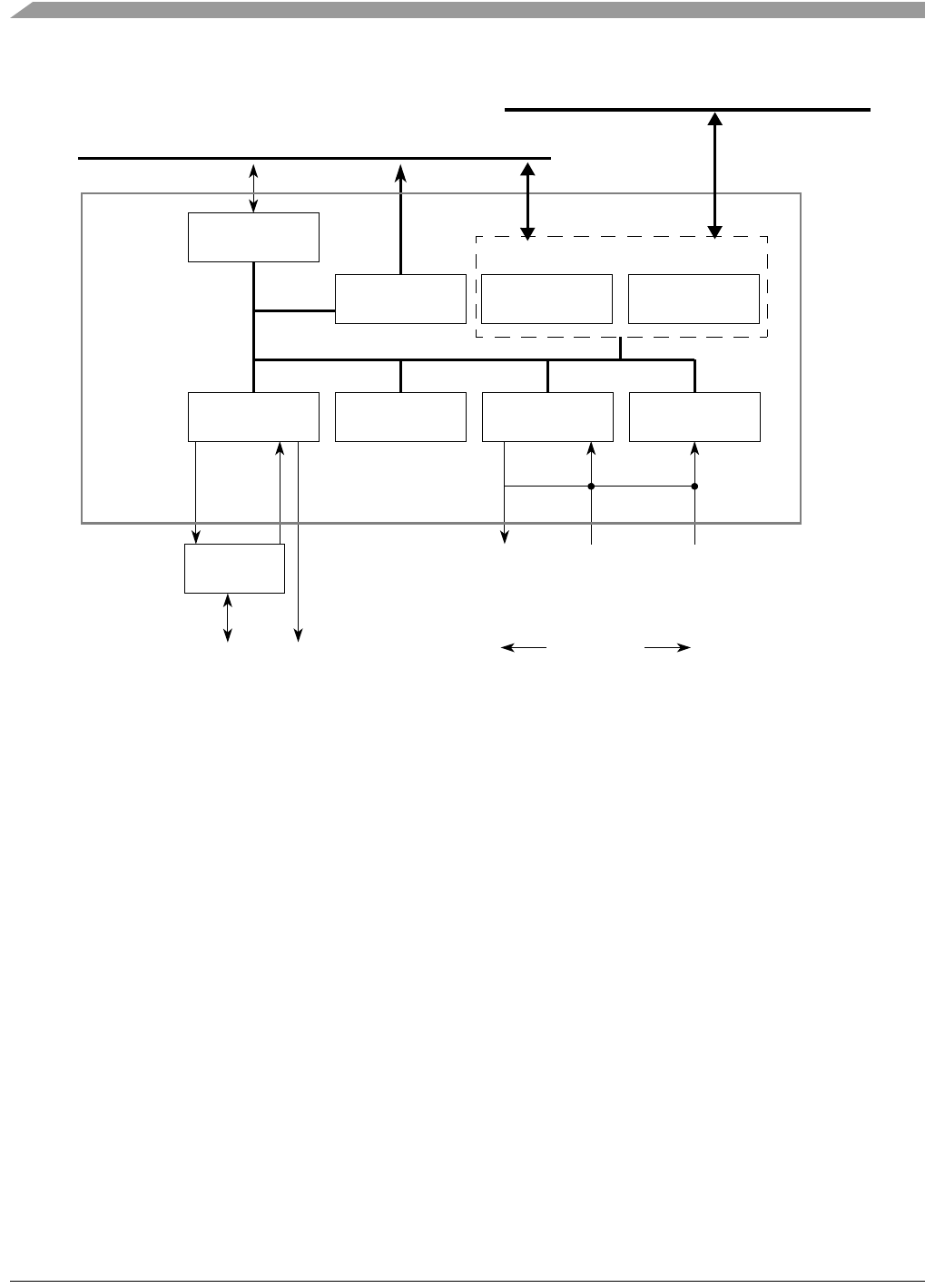
MCF548x Reference Manual, Rev. 3
30-2 Freescale Semiconductor
Figure 30-1. FEC Block Diagram
30.1.3 Overview
The Fast Ethernet Controller is designed to support both 10 and 100 Mbps Ethernet/IEEE 802.3 networks.
An external transceiver interface and transceiver function are required to complete the interface to the
media. The FEC supports three different standard MAC-PHY (physical) interfaces for connection to an
external Ethernet transceiver. The FEC supports the 10/100 Mbps MII and the 10 Mbps-only 7-wire
interface, which uses a subset of the MII pins. The user controls the FEC by writing the control registers
within the CSR (control and status register) block. The CSR provides global control (e.g. Ethernet reset
and enable) and interrupt handling registers.
The MII block provides a serial channel for control/status communication with the external physical layer
device (transceiver). This serial channel consists of the EMDC (management data clock) and EMDIO
(management data input/output) lines of the MII interface.
The transmit and receive blocks provide the Ethernet MAC functionality (with some assist from
microcode). The transmit and receive FIFOs are 1024 bytes each.
The message information block (MIB) maintains counters for a variety of network events and statistics. It
is not necessary for operation of the FEC but provides valuable counters for network management. The
counters supported are the RMON (RFC 1757) Ethernet Statistics group and some of the IEEE 802.3
counters. See Section 30.3.3, “MIB Block Counters Memory Map,” for more information.
I/O
Pad
EnMDIO EnMDC
EnTXEN
EnTXD[3:0]
EnTXER
EnTXCLK
EnCRS EnRXCLK
EnRXDV
EnRXD[3:0]
EnRXER
MII/7-Wire
Data Option
EnCOL
FEC
CSR
Slave
Interface
MII MIB
Counters Transmit Receive
FIFO
Transmit FIFO
Receive
FIFO Controller
Interrupt
EnMDIO
EnMDEN EnMDIO
IP Bus
Comm Bus

Introduction
MCF548x Reference Manual, Rev. 3
Freescale Semiconductor 30-3
30.1.4 Features
The FEC incorporates the following features:
• Support for three different Ethernet physical interfaces:
— 100-Mbps IEEE 802.3 MII
— 10-Mbps IEEE 802.3 MII
— 10-Mbps 7-wire interface
• IEEE 802.3 full duplex flow control
• Programmable max frame length supports IEEE 802.1 VLAN tags and priority
• Support for full-duplex operation (200Mbps throughput) with a minimum system clock rate of
50MHz
• Support for half-duplex operation (100Mbps throughput) with a minimum system clock rate of 25
MHz
• Retransmission from transmit FIFO following a collision (no processor bus utilization)
• Address recognition
— Frames with broadcast address may be always accepted or always rejected
— Exact match for single 48-bit individual (unicast) address
— Hash (64-bit hash) check of individual (unicast) addresses
— Hash (64-bit hash) check of group (multicast) addresses
— Promiscuous mode
30.1.5 Modes of Operation
The primary operational modes are described in this section.
30.1.5.1 Full and Half Duplex Operation
Full duplex mode is intended for use on point to point links between switches or end node to switch. Half
duplex mode is used in connections between an end node and a repeater or between repeaters. Selection
of the duplex mode is controlled by TCR[FDEN] and RCR[DRT].
When configured for full duplex mode, flow control may be enabled. Refer to the TCR[RFC_PAUSE] and
TCR[TFC_PAUSE] bits, the RCR[FCE] bit, and Section 30.4.8, “Full Duplex Flow Control,” for more
details.
30.1.5.2 Interface Options
The following interface options are supported. A detailed discussion of the interface configurations is
provided in Section 30.4.3, “Network Interface Options”.
30.1.5.2.1 10 Mbps and 100 Mbps MII Interface
MII is the Media Independent Interface defined by the IEEE 802.3 standard for 10/100 Mbps operation.
The MAC-PHY interface may be configured to operate in MII mode by asserting RCR[MII_MODE].
The speed of operation is determined by the ETXCLK and ERXCLK signals which are driven by the
external transceiver. The transceiver will either auto-negotiate the speed or it may be controlled by
software via the serial management interface (EMDC/EMDIO signals) to the transceiver. Refer to the
MMFR and MSCR register descriptions as well as the description of how to read and write registers in the

MCF548x Reference Manual, Rev. 3
30-4 Freescale Semiconductor
transceiver via this interface in the following sections: Section 30.4.3, “Network Interface Options,”
Section 30.4.13, “MII Data Frame,” and Section 30.4.14, “MII Management Frame Structure.”
30.1.5.2.2 10 Mpbs 7-Wire Interface Operation
The FEC supports a 7-wire interface as used by many 10 Mbps Ethernet transceivers. The
RCR[MII_MODE] bit controls this functionality. If this bit is deasserted, the MII mode is disabled and the
10 Mbps, 7-wire mode is enabled.
30.1.5.3 Address Recognition Options
The address options supported are promiscuous, broadcast reject, individual address (hash or exact match),
and multicast hash match. Address recognition options are discussed in detail in Section 30.4.6, “Ethernet
Address Recognition”.
30.1.5.4 Internal Loopback
Internal loopback mode is selected via RCR[LOOP]. Loopback mode is discussed in detail in
Section 30.4.11, “Internal and External Loopback”.
30.2 External Signals
The MII interface consists of 18 signals. The transmit and receive functions require seven signals each,
four data signals, a delimiter, error, and clock. In addition, there are two signals which indicate the status
of the media, one indicates the presence of a carrier, and the second one indicates that a collision has
occurred. The remaining two signals provide a management interface. Each MII signal is described below.
30.2.1 Transmit Clock (EnTXCLK)
EnTXCLK is a continuous input clock that provides a timing reference for EnTXEN, EnTXD, and
EnTXER.
30.2.2 Receive Clock (EnRXCLK)
EnRXCLK is a continuous input clock which provides a timing reference for EnRXDV, EnRXD, and
EnRXER.
30.2.3 Transmit Enable (EnTXEN)
Assertion of this output signal indicates that there are valid nibbles being presented on the MII. This signal
is asserted with the first nibble of preamble and is negated prior to the first EnTXCLK following the final
nibble of the frame.
30.2.4 Transmit Data[3:0] (EnTXD[3:0])
EnTXD[3:0] represent a nibble of data when EnTXEN is asserted and have no meaning when EnTXEN is
de-asserted. EnTXD0 is used for serial data in 7-wire mode. Table 30-2 summarizes the permissible
encoding of EnTXD.

External Signals
MCF548x Reference Manual, Rev. 3
Freescale Semiconductor 30-5
30.2.5 Transmit Error (EnTXER)
Assertion of this output signal for one or more clock cycles while EnTXEN is asserted shall cause the PHY
to transmit one or more illegal symbols. Asserting EnTXER has no affect when operating at 10 Mbps or
when EnTXEN is de-asserted This signal transitions synchronously with respect to EnTXCLK.
30.2.6 Receive Data Valid (EnRXDV)
When this input signal is asserted, the PHY is indicating that a valid nibble is present on the MII. This
signal shall remain asserted from the first recovered nibble of the frame through the last nibble. Assertion
of EnRXDV must start no later than the Start of Frame delimiter (SFD), and exclude any End of Frame
delimiter (EOF).
30.2.7 Receive Data[3:0] (EnRXD[3:0])
EnRXD[3:0] represents a nibble of data to be transferred from the PHY to the MAC when EnRXDV is
asserted. A completely formed SFD must be passed across the MII. When EnRXDV is not asserted,
EnRXD has no meaning. There is an exception to this which is explained later. Table 30-3 summarizes the
permissible encoding of EnRXD. EnRXD0 is used for serial data in 7-wire mode.
30.2.8 Receive Error (EnRXER)
When EnRXER and EnRXDV are asserted, the PHY has detected an error in the current frame. When
EnRXDV is not asserted, EnRXER shall have no affect. This signal transitions synchronously with
EnRXCLK
30.2.9 Carrier Sense (EnCRS)
This input signal is asserted when the transmit or receive medium is not idle. In the event of a collision,
EnCRS will remain asserted through the duration of the collision. This signal is not required to transition
synchronously with EnTXCLK or EnRXCLK.
30.2.10 Collision (EnCOL)
This input signal is asserted upon detection of a collision, and will remain asserted while the collision
persists. The behavior of this signal is not specified when in Full Duplex mode. This signal is not required
to transition synchronously with EnTXCLK or EnRXCLK.
30.2.11 Management Data Clock (EnMDC)
This signal provides a timing reference to the PHY for data transfers on the EnMDIO signal. EnMDC is
aperiodic, and has no maximum high or low times. The minimum high and low times is 160ns, with the
minimum period being 400ns.
30.2.12 Management Data (EnMDIO)
This signal transfers control/status information between the PHY and MAC. It transitions synchronously
to EnMDC. The EnMDIO pin is a bidirectional pin.
Table 30-2 below provides the interpretation of the possible encodings of EnTXEN, EnTXER.

MCF548x Reference Manual, Rev. 3
30-6 Freescale Semiconductor
.
A false carrier condition occurs if the PHY detects a bad start-of-stream delimiter. This condition is
signaled to the MII by asserting EnRXER and placing 1110 on EnRXD. EnRXDV must also be
de-asserted. The valid encodings of EnRXDV, EnRXER and EnRXD[3:0] are shown in Table 30-3 below.
30.3 Memory Map/Register Definition
This section gives an overview of the FEC registers. The FEC is programmed by control/status registers
(CSRs). The CSRs are used for mode control and to extract global status information.
30.3.1 Top Level Module Memory Map
The FEC implementation occupies a 1-Kbyte memory map space. This is divided into two sections of 512
bytes each. The first is used for control/status registers. The second contains event/statistic counters held
in the MIB block. Table 30-4 defines the top level memory map.
Table 30-2. MII: Valid Encoding of EnTXD, EnTXEN and EnTXER
EnTXEN EnTXER EnTXD[3:0] Indication
0 0 0000 through 1111 Normal inter-frame
0 1 0000 through 1111 Reserved
1 0 0000 through 1111 Normal data transmission
1 1 0000 through 1111 Transmit error
propagation
Table 30-3. MII: Valid Encoding of EnRXD, EnRXER and EnRXDV
EnRXDV EnRXER EnRXD[3:0] Indication
0 0 0000 through 1111 Normal inter-frame
0 1 0000 Normal inter-frame
0 1 0001 through 1101 Reserved
0 1 1110 False Carrier
0 1 1111 Reserved
1 0 0000 through 1111 Normal Data Reception
1 1 0000 through 1111 Data reception with errors
Table 30-4. Module Memory Map
Address Function
MBAR + 0x9000–91FF FEC 0 Control/Status Registers
MBAR + 0x9200–93FF FEC 0 MIB Block Counters
MBAR + 0x9800–99FF FEC 1 Control/Status Registers
MBAR + 0x9A00–9BFF FEC 1 MIB Block Counters

Memory Map/Register Definition
MCF548x Reference Manual, Rev. 3
Freescale Semiconductor 30-7
30.3.2 Detailed Memory Map (Control/Status Registers)
Table 30-5 shows the FEC register memory map with each register address, name, and a brief description.
Table 30-5. FEC Register Memory Map
MBAR
Offset for
FEC0
MBAR
Offset for
FEC1
Name Byte 0 Byte 1 Byte 2 Byte 3
0x9000 0x9800 Reserved
0x9004 0x9804 Ethernet Interrupt Event Register EIR
0x9008 0x9808 Ethernet Interrupt Mask Register EIMR
0x900C–
0x9020
0x980C–
0x9820
Reserved
0x9024 0x9824 Ethernet Control Register ECR
0x9028–
0x903C
0x9828–
0x983C
Reserved
0x9040 0x9840 MII Data Register MDATA
0x9044 0x9844 MII Speed Control Register MSCR
0x9048–
0x9060
0x9848–
0x9860
Reserved
0x9064 0x9864 MIB Control/Status Register MIBC
0x9068–
0x9080
0x9068–
0x9880
Reserved
0x9084 0x9884 Receive Control Register RCR
0x9088 0x9888 Receive Hash Register RHR
0x908C–
0x90C0
0x988C–
0x98C0
Reserved
0x90C4 0x98C4 Transmit Control Register TCR
0x90C8–
0x90E0
0x98C8–
0x98E0
Reserved
0x90E4 0x98E4 Physical Address Low Register PALR
0x90E8 0x98E8 Physical Address High Register PAHR
0x90EC 0x98EC Opcode / Pause Duration Register OPD
0x90F0–
-0x9114
0x98F0–
-0x9814
Reserved
0x9118 0x9918 Individual Address Upper Register IAUR
0x911C 0x991C Individual Address Lower Register IALR
0x9120 0x9920 Group Address Upper Register GAUR
0x9124 0x9924 Group Address Lower Register GALR

MCF548x Reference Manual, Rev. 3
30-8 Freescale Semiconductor
30.3.3 MIB Block Counters Memory Map
Table 30-6 defines the MIB Counters memory map which defines the locations in the MIB RAM space
where hardware maintained counters reside. These fall in the 0x9200–0x93FF address offset range for
FEC0 and the 0x9A00–0x9BFF address offset range for FEC1. The counters are divided into two groups.
RMON counters are included which cover the Ethernet statistics counters defined in RFC 1757. In addition
to the counters defined in the Ethernet statistics group, a counter is included to count truncated frames as
the FEC only supports frame lengths up to 2047 bytes. The RMON counters are implemented
independently for transmit and receive to insure accurate network statistics when operating in full duplex
mode.
IEEE counters are included which support the mandatory and recommended counter packages defined in
Section 5 of ANSI/IEEE Std. 802.3 (1998 edition). The IEEE Basic Package objects are supported by the
FEC but do not require counters in the MIB block. In addition, some of the recommended package objects
0x9128–
0x9140
0x9828–
0x9840
Reserved
0x9144 0x9944 FEC Transmit FIFO Watermark FECTFWR
0x9184 0x9984 FEC Receive FIFO Data Register FECRFDR
0x9188 0x9988 FEC Receive FIFO Status Register FECRFSR
0x918C 0x998C FEC Receive FIFO Control Register FECRFCR
0x9190 0x9990 FEC Receive FIFO Last Read Frame Pointer FECRLRFP
0x9194 0x9994 FEC Receive FIFO Last Write Frame Pointer FECRLWFP
0x9198 0x9998 FEC Receive FIFO Alarm Register FECRFAR
0x919C 0x999C FEC Receive FIFO Read Pointer Register FECRFRP
0x91A0 0x99A0 FEC Receive FIFO Write Pointer Register FECRFWP
0x91A4 0x99A4 FEC Transmit FIFO Data Register FECTFDR
0x91A8 0x99A8 FEC Transmit FIFO Status Register FECTFSR
0x91AC 0x99AC FEC Transmit FIFO Control Register FECTFCR
0x91B0 0x99B0 FEC Transmit FIFO Last Read Frame Pointer FECTLRFP
0x91B4 0x99B4 FEC Transmit FIFO Last Write Frame Pointer FECTLWFP
0x91B8 0x99B8 FEC Transmit FIFO Alarm Register FECTFAR
0x91BC 0x99BC FEC Transmit FIFO Read Pointer Register FECTFRP
0x91C0 0x99C0 FEC Transmit FIFO Write Pointer Register FECTFWP
0x91C4 0x99C4 FIFO Reset Register FECFRST
0x91C8 0x99C8 CRC and Transmit Frame Control Word Register FECCTCWR
Table 30-5. FEC Register Memory Map (Continued)
MBAR
Offset for
FEC0
MBAR
Offset for
FEC1
Name Byte 0 Byte 1 Byte 2 Byte 3

Memory Map/Register Definition
MCF548x Reference Manual, Rev. 3
Freescale Semiconductor 30-9
which are supported do not require MIB counters. Counters for transmit and receive full duplex flow
control frames are included as well.
Table 30-6. MIB Counters Memory Map
MBAR Offset
for FEC0
MBAR Offset
for FEC1 Mnemonic Description
0x9200 0x9A00 RMON_T_DROP Count of frames not counted correctly
0x9204 0x9A04 RMON_T_PACKETS RMON Tx packet count
0x9208 0x9A08 RMON_T_BC_PKT RMON Tx Broadcast Packets
0x920C 0x9A0C RMON_T_MC_PKT RMON Tx Multicast Packets
0x9210 0x9A10 RMON_T_CRC_ALIGN RMON Tx Packets w CRC/Align error
0x9214 0x9A14 RMON_T_UNDERSIZE RMON Tx Packets < 64 bytes, good crc
0x9218 0x9A18 RMON_T_OVERSIZE RMON Tx Packets > MAX_FL bytes, good crc
0x921C 0x9A1C RMON_T_FRAG RMON Tx Packets < 64 bytes, bad crc
0x9220 0x9A20 RMON_T_JAB RMON Tx Packets > MAX_FL bytes, bad crc
0x9224 0x9A24 RMON_T_COL RMON Tx collision count
0x9228 0x9A28 RMON_T_P64 RMON Tx 64 byte packets
0x922C 0x9A2C RMON_T_P65TO127 RMON Tx 65 to 127 byte packets
0x9230 0x9A30 RMON_T_P128TO255 RMON Tx 128 to 255 byte packets
0x9234 0x9A34 RMON_T_P256TO511 RMON Tx 256 to 511 byte packets
0x9238 0x9A38 RMON_T_P512TO1023 RMON Tx 512 to 1023 byte packets
0x923C 0x9A3C RMON_T_P1024TO2047 RMON Tx 1024 to 2047 byte packets
0x9240 0x9A40 RMON_T_P_GTE2048 RMON Tx packets w > 2048 bytes
0x9244 0x9A44 RMON_T_OCTETS RMON Tx Octets
0x9248 0x9A48 IEEE_T_DROP Count of frames not counted correctly
0x924C 0x9A4C IEEE_T_FRAME_OK Frames Transmitted OK
0x9250 0x9A50 IEEE_T_1COL Frames Transmitted with Single Collision
0x9254 0x9A54 IEEE_T_MCOL Frames Transmitted with Multiple Collisions
0x9258 0x9A58 IEEE_T_DEF Frames Transmitted after Deferral Delay
0x925c 0x9A5c IEEE_T_LCOL Frames Transmitted with Late Collision
0x9260 0x9A60 IEEE_T_EXCOL Frames Transmitted with Excessive Collisions
0x9264 0x9A64 IEEE_T_MACERR Frames Transmitted with Tx FIFO Underrun
0x9268 0x9A68 IEEE_T_CSERR Frames Transmitted with Carrier Sense Error
0x926C 0x9A6C IEEE_T_SQE Frames Transmitted with SQE Error
0x9270 0x9A70 IEEE_T_FDXFC Flow Control Pause frames transmitted
0x9274 0x9A74 IEEE_T_OCTETS_OK Octet count for Frames Transmitted w/o Error

MCF548x Reference Manual, Rev. 3
30-10 Freescale Semiconductor
30.3.3.1 Ethernet Interrupt Event Register (EIR)
When an event occurs that sets a bit in the EIR, an interrupt will be generated if the corresponding bit in
the interrupt mask register (EIMR) is also set. The bit in the EIR is cleared if a one is written to that bit
position; writing zero has no effect. This register is cleared upon hardware reset.
These interrupts can be divided into operational interrupts, transceiver/network error interrupts, and
internal error interrupts. Interrupts which may occur in normal operation are GRA, TXF, and MII.
0x9278–
0x927C
0x9A78–
0x9A7C
Reserved
0x9280 0x9A80 RMON_R_DROP Count of frames not counted correctly
0x9284 0x9A84 RMON_R_PACKETS RMON Rx packet count
0x9288 0x9A88 RMON_R_BC_PKT RMON Rx Broadcast Packets
0x928C 0x9A8C RMON_R_MC_PKT RMON Rx Multicast Packets
0x9290 0x9A90 RMON_R_CRC_ALIGN RMON Rx Packets w CRC/Align error
0x9294 0x9A94 RMON_R_UNDERSIZE RMON Rx Packets < 64 bytes, good crc
0x9298 0x9A98 RMON_R_OVERSIZE RMON Rx Packets > MAX_FL bytes, good crc
0x929C 0x9A9C RMON_R_FRAG RMON Rx Packets < 64 bytes, bad crc
0x92A0 0x9AA0 RMON_R_JAB RMON Rx Packets > MAX_FL bytes, bad crc
0x92A4 0x9AA4 RMON_R_RESVD_0
0x92A8 0x9AA8 RMON_R_P64 RMON Rx 64 byte packets
0x92AC 0x9AAC RMON_R_P65TO127 RMON Rx 65 to 127 byte packets
0x92B0 0x9AB0 RMON_R_P128TO255 RMON Rx 128 to 255 byte packets
0x92B4 0x9AB4 RMON_R_P256TO511 RMON Rx 256 to 511 byte packets
0x92B8 0x9AB8 RMON_R_P512TO1023 RMON Rx 512 to 1023 byte packets
0x92BC 0x9ABC RMON_R_P1024TO2047 RMON Rx 1024 to 2047 byte packets
0x92C0 0x9AC0 RMON_R_P_GTE2048 RMON Rx packets w > 2048 bytes
0x92C4 0x9AC4 RMON_R_OCTETS RMON Rx Octets
0x92C8 0x9AC8 IEEE_R_DROP Count of frames not counted correctly
0x92CC 0x9ACC IEEE_R_FRAME_OK Frames Received OK
0x92D0 0x9AD0 IEEE_R_CRC Frames Received with CRC Error
0x92D4 0x9AD4 IEEE_R_ALIGN Frames Received with Alignment Error
0x92D8 0x9AD8 IEEE_R_MACERR Receive Fifo Overflow count
0x92DC 0x9ADC IEEE_R_FDXFC Flow Control Pause frames received
0x92E0 0x9AE0 IEEE_R_OCTETS_OK Octet count for Frames Rcvd w/o Error
Table 30-6. MIB Counters Memory Map (Continued)
MBAR Offset
for FEC0
MBAR Offset
for FEC1 Mnemonic Description

Memory Map/Register Definition
MCF548x Reference Manual, Rev. 3
Freescale Semiconductor 30-11
Interrupts resulting from errors/problems detected in the network or transceiver are HBERR, BABR,
BABT, LC, and RL. Interrupts resulting from internal errors are HBERR, XFUN, XFERR, and RFERR.
Some of the error interrupts are independently counted in the MIB block counters. Software may choose
to mask off these interrupts because these errors will be visible to network management via the MIB
counters.
• HBERR – IEEE_T_SQE
• BABR – RMON_R_OVERSIZE (good CRC), RMON_R_JAB (bad CRC)
• BABT – RMON_T_OVERSIZE (good CRC), RMON_T_JAB (bad CRC)
• LC – IEEE_T_LCOL
• RL – IEEE_T_EXCOL
• XFUN – IEEE_T_MACERR
31 30 29 28 27 26 25 24 23 22 21 20 19 18 17 16
R HBERR BABR BABT GRA TXF 0 0 0 MII 0 LC RL XFUN XFERR RFERR 0
Ww1c w1c w1c w1c w1c w1c w1c w1c w1c w1c w1c
Reset0 000000000000 0 0 0
15 14 13 12 11 10 9 8 7 6 5 4 3 2 1 0
R0 000000000000 0 0 0
W
Reset0 000000000000 0 0 0
Reg
Addr
MBAR + 0x9004 (FEC0), 0x9804 (FEC1)
Figure 30-2. Ethernet Interrupt Event Register (EIR)
Table 30-7. EIR Descriptions
Bits Name Description
31 HBERR Heartbeat error. This interrupt indicates that HBC is set in the TCR register and that the ECOL input
was not asserted within the Heartbeat window following a transmission. This bit is cleared by writing
a 1 to it.
30 BABR Babbling receive error. This bit indicates a frame was received with length in excess of
RCR[MAX_FL] bytes. This bit is cleared by writing a 1 to it.
29 BABT Babbling transmit error. This bit indicates that the transmitted frame length has exceeded
RCR[MAX_FL] bytes. This condition is usually caused by a frame that is too long being placed into
the transmit data buffers. Truncation does not occur. This bit is cleared by writing a 1 to it.
28 GRA Graceful stop complete. This interrupt will be asserted for one of three reasons. Graceful stop
means that the transmitter is put into a pause state after completion of the frame currently being
transmitted.
1) A graceful stop, which was initiated by the setting of the TCR[GTS] bit is now complete.
2) A graceful stop, which was initiated by the setting of the TCR[TFC_PAUSE] bit is now complete.
3) A graceful stop, which was initiated by the reception of a valid full duplex flow control “pause”
frame is now complete. Refer to Section 30.4.8, “Full Duplex Flow Control” .
This bit is cleared by writing a 1 to it.
27 TXF Transmit frame interrupt. This bit indicates that a frame has been transmitted. This bit is cleared by
writing a 1 to it.

MCF548x Reference Manual, Rev. 3
30-12 Freescale Semiconductor
30.3.3.2 Interrupt Mask Register (EIMR)
The EIMR controls which possible interrupt events are allowed to generate actual interrupts. All
implemented bits in this CSR are read/write. This register is cleared upon a hardware reset. If the
corresponding bits in both the EIR and EIMR registers are set, the interrupt will be signalled to the on chip
interrupt controller. The interrupt signal will remain asserted until a 1 is written to the EIR bit (write 1 to
clear) or a 0 is written to the EIMR bit.
26–24 — Reserved, should be cleared.
23 MII MII interrupt. This bit indicates that the MII has completed the data transfer requested. This bit is
cleared by writing a 1 to it.
22 — Reserved, should be cleared.
21 LC Late collison. This bit indicates that a collision occurred beyond the collision window (slot time) in
half duplex mode. The frame is truncated with a bad CRC and the remainder of the frame is
discarded. This bit is cleared by writing a 1 to it.
20 RL Collision retry limit. This bit indicates that a collision occurred on each of 16 successive attempts to
transmit the frame. The frame is discarded without being transmitted and transmission of the next
frame will commence. Can only occur in half duplex mode. This bit is cleared by writing a 1 to it.
19 XFUN Transmit FIFO underrun. This bit indicates that the transmit FIFO became empty before the
complete frame was transmitted. A bad CRC is appended to the frame fragment and the remainder
of the frame is discarded. This bit is cleared by writing a 1 to it.
18 XFERR Transmit FIFO error. This bit indicates that an error has occurred within the transmit FIFO. When the
XFERR bit is set, ECR[ETHER_EN] will be cleared, halting frame processing by the FEC. When this
occurs, software will need to generate a software reset of the FIFO controller. This bit is cleared by
writing a 1 to it.
17 RFERR Receive FIFO error. This bit indicates that an error has occurred within the receive FIFO. When the
RFERR bit is set, ECR[ETHER_EN] will be cleared, halting frame processing by the FEC. When this
occurs, software will need to generate a software reset of the FIFO controller. This bit is cleared by
writing a 1 to it.
16–0 — Reserved, should be cleared.
Table 30-7. EIR Descriptions (Continued)
Bits Name Description

Memory Map/Register Definition
MCF548x Reference Manual, Rev. 3
Freescale Semiconductor 30-13
30.3.3.3 Ethernet Control Register (ECR)
ECR is a read/write user register, though both fields in this register may be altered by hardware as well.
The ECR is used to enable/disable the FEC.
31 30 29 28 27 26 25 24 23 22 21 20 19 18 17 16
R HBERR BABR BABT GRA TXF 0 0 0 MII 0 LC RL XFUN XFERR RFERR 0
W
Reset0 000000000000 0 0 0
1514131211109876543 2 1 0
R0 000000000000 0 0 0
W
Reset0 000000000000 0 0 0
Reg
Addr
MBAR + 0x9008 (FEC0), 0x9808 (FEC1)
Figure 30-3. Ethernet Interrupt Mask Register (EIMR)
Table 30-8. EIMR Field Descriptions
Bits Name Description
31–27,
23, 21–17
See Figure 30-3
and Table 30-7.
Interrupt mask. Each bit corresponds to an interrupt source defined by the EIR register. The
corresponding EIMR bit determines whether an interrupt condition can generate an interrupt.
At every processor clock, the EIR samples the signal generated by the interrupting source. The
corresponding EIR bit reflects the state of the interrupt signal even if the corresponding EIMR
bit is set.
0 The corresponding interrupt source is masked.
1 The corresponding interrupt source is not masked.
26–24,
22, 16–0
— Reserved, should be cleared.
31 30 29 28 27 26 25 24 23 22 21 20 19 18 17 16
R00000000000000 0 0
W
Reset11110000000000 0 0
15141312111098765432 1 0
R00000000000000ETHER
_EN
RESET
W
Reset00000000000000 0 0
Reg
Addr
MBAR + 0x9024 (FEC0), 0x9824 (FEC1)
Figure 30-4. Ethernet Control Register (ECR)

MCF548x Reference Manual, Rev. 3
30-14 Freescale Semiconductor
30.3.3.4 MII Management Frame Register (MMFR)
The MMFR is accessed by the user and does not reset to a defined value. The MMFR register is used to
communicate with the attached MII compatible PHY devices, providing read/write access to their MII
registers. Performing a write to the MMFR will cause a management frame to be sourced unless the MSCR
has been programmed to 0. In the case of writing to MMFR when MSCR = 0, if the MSCR register is then
written to a non-zero value, an MII frame will be generated with the data previously written to the MMFR.
This allows MMFR and MSCR to be programmed in either order if MSCR is currently zero.
Table 30-9. ECR Field Descriptions
Bits Name Description
31–2 — Reserved, should be cleared.
1 ETHER_EN When this bit is set, the FEC is enabled, and reception and transmission are possible. When this
bit is cleared, reception is immediately stopped and transmission is stopped after a bad CRC is
appended to any currently transmitted frame. The ETHER_EN bit is altered by hardware under the
following conditions:
• ECR[RESET] is set by software, in which case ETHER_EN will be cleared
• An error condition causes the EIR[XFERR], or EIR[RFERR] bits to set, in which case
ETHER_EN will be cleared
0 RESET When this bit is set, the equivalent of a hardware reset is performed but it is local to the FEC.
ETHER_EN is cleared and all other FEC registers take their reset values. Also, any
transmission/reception currently in progress is abruptly aborted. This bit is automatically cleared by
hardware during the reset sequence. The reset sequence takes approximately 8 system clock
cycles after RESET is written with a 1.
31 30 29 28 27 26 25 24 23 22 21 20 19 18 17 16
RST OP PA RA TA
W
Reset Uninitialized
1514131211109876543210
RDATA
W
Reset Uninitialized
Reg
Addr
MBAR + 0x9040 (FEC0), 0x9840 (FEC1)
Figure 30-5. MII Management Frame Register (MMFR)
Table 30-10. MMFR Field Descriptions
Bit Name Description
31–30 ST Start of frame delimiter. These bits must be programmed to 0x01 for a valid MII management
frame.
29–28 OP Operation code. This field must be programmed to 0x10 (read) or 0x01 (write) to generate a valid
MII management frame. A value of 0x11 will produce “read” frame operation while a value of 0x00
will produce “write” frame operation, but these frames will not be MII compliant.

Memory Map/Register Definition
MCF548x Reference Manual, Rev. 3
Freescale Semiconductor 30-15
To perform a read or write operation on the MII Management Interface, the MMFR register must be
written by the user. To generate a valid read or write management frame, the ST field must be written with
a 01 pattern, and the TA field must be written with a 10. If other patterns are written to these fields, a frame
will be generated but will not comply with the IEEE 802.3 MII definition.
If the MMFR is written while frame generation is in progress, the frame contents will be altered. Software
should use the MII interrupt to avoid writing to the MMFR register while frame generation is in progress.
30.3.3.4.1 Generating a Write Frame
To generate an IEEE 802.3-compliant MII Management Interface write frame (write to a PHY register),
the user must write {01 01 PHYAD REGAD 10 DATA} to the MMFR register. Writing this pattern will
cause the control logic to shift out the data in the MMFR register following a preamble generated by the
control state machine. During this time the contents of the MMFR register will be altered as the contents
are serially shifted and will be unpredictable if read by the user. Once the write management frame
operation has completed, the MII interrupt will be generated. At this time the contents of the MMFR
register will match the original value written.
30.3.3.4.2 Generating a Read Frame
To generate an MII Management Interface read frame (read a PHY register) the user must write {01 10
PHYAD REGAD 10 XXXX} to the MMFR register (the content of the DATA field is a don’t care). Writing
this pattern will cause the control logic to shift out the data in the MMFR register following a preamble
generated by the control state machine. During this time the contents of the MMFR register will be altered
as the contents are serially shifted, and will be unpredictable if read by the user. Once the read management
frame operation has completed, the MII interrupt will be generated. At this time the contents of the MMFR
register will match the original value written except for the DATA field whose contents have been replaced
by the value read from the PHY register.
30.3.3.5 MII Speed Control Register (MSCR)
The MSCR provides control of the MII clock (EMDC signal) frequency and allows dropping the preamble
on the MII management frame.
27–23 PA PHY address. This field specifies one of up to 32 attached PHY devices.
22–18 RA Register address. This field specifies one of up to 32 registers within the specified PHY device.
17–16 TA Turn around. This field must be programmed to 0x10 to generate a valid MII management frame.
15–0 DATA Management frame data. This is the field for data to be written to or read from the PHY register.
Table 30-10. MMFR Field Descriptions (Continued)
Bit Name Description

MCF548x Reference Manual, Rev. 3
30-16 Freescale Semiconductor
The MII_SPEED field must be programmed with a value to provide an EMDC frequency of less than or
equal to 2.5 MHz to be compliant with the IEEE 802.3 MII specification. The MII_SPEED must be set to
a non-zero value in order to source a read or write management frame. After the management frame is
complete the MSCR register may optionally be set to zero to turn off the EMDC. The EMDC generated
will have a 50% duty cycle except when MII_SPEED is changed during operation (change will take effect
following either a rising or falling edge of EMDC).
If the system clock is 66 MHz, programming the MII_SPEED field to 0x5 will result in an EMDC
frequency of 66 MHz × 1/26 = 2.5 MHz. A table showing optimum values for MII_SPEED as a function
of system clock frequency is provided below.
31 30 29 28 27 26 25 24 23 22 21 20 19 18 17 16
R00000000 0 0000000
W
Reset00000000 0 0000000
15 14 13 12 11 10 9 8 7 6 5 4 3 2 1 0
R00000000DIS_PRE
AMBLE
MII_SPEED 0
W
Reset00000000 0 0000000
Reg
Addr
MBAR + 0x9044 (FEC0), 0x9844 (FEC1)
Figure 30-6. MII Speed Control Register (MSCR)
Table 30-11. MSCR Field Descriptions
Bits Name Description
31–8 — Reserved, should be cleared.
7DIS_PRE
AMBLE
Asserting this bit will cause preamble (32 1’s) not to be prepended to the MII management
frame. The MII standard allows the preamble to be dropped if the attached PHY devices
do not require it.
6–1 MII_SPEED MII_SPEED controls the frequency of the MII management interface clock (EMDC) relative
to the system clock (which for the FEC module is the IP bus). A value of 0 in this field will
“turn off” the EMDC and leave it in low voltage state. Any non-zero value will result in the
EMDC frequency of 1/(MII_SPEED*2) of the system clock frequency.
0 — Reserved, should be cleared.
Table 30-12. Programming Examples for MSCR
Clock Frequency MII_SPEED (field in reg) EMDC frequency
60 MHz 0xC 2.5 MHz
66 MHz 0xD 2.5 MHz
120 MHz 0x18 2.5 MHz
133 MHz 0x1A 2.5 MHz
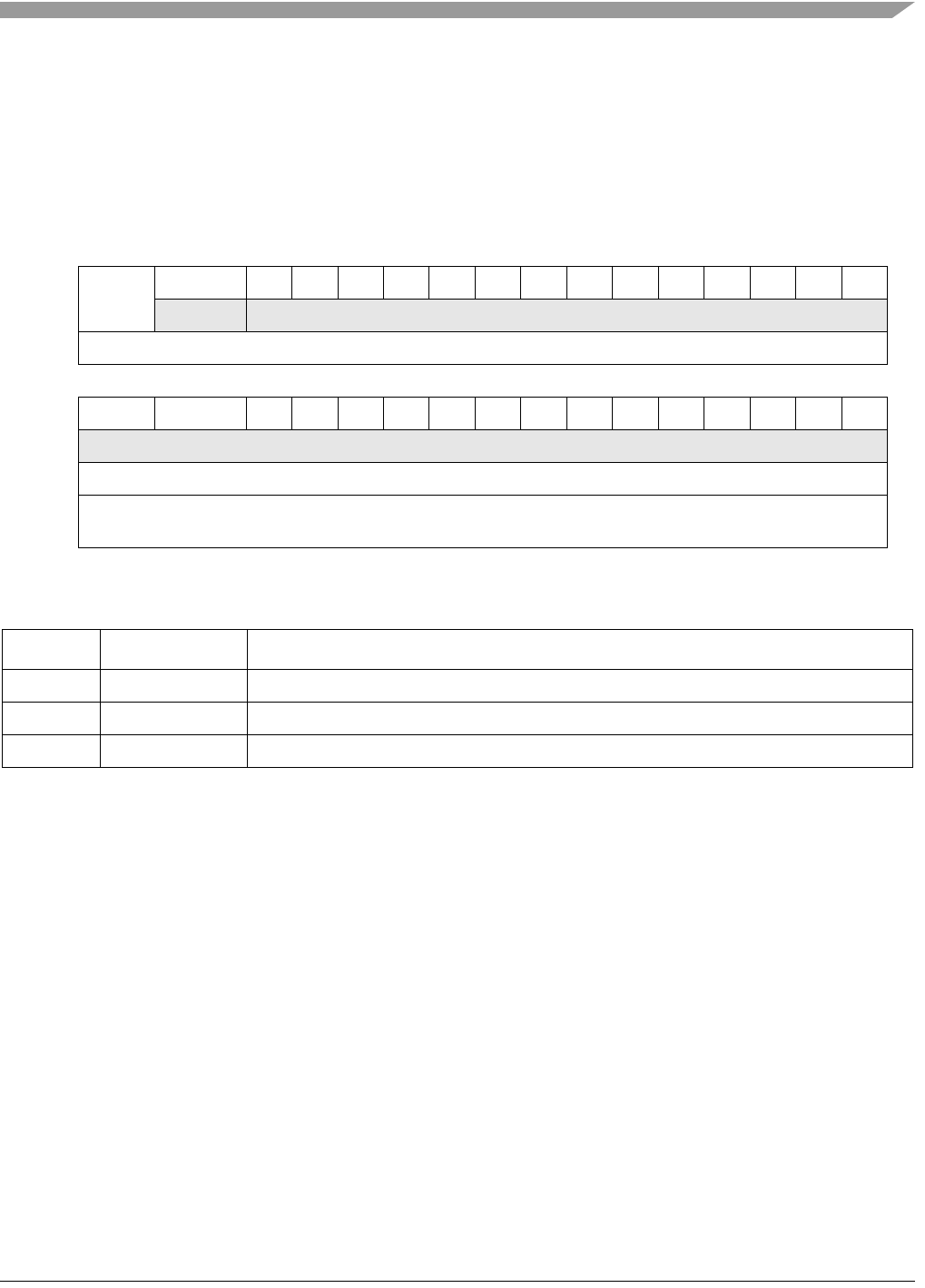
Memory Map/Register Definition
MCF548x Reference Manual, Rev. 3
Freescale Semiconductor 30-17
30.3.3.6 MIB Control Register (MIBC)
The MIBC is a read/write register used to provide control of and to observe the state of the MIB block.
This register is accessed by user software if there is a need to disable the MIB block operation. For
example, in order to clear all MIB counters in RAM the user should disable the MIB block, then clear all
the MIB RAM locations, then enable the MIB block. The MIB_DISABLE bit is reset to 1. See Table 30-6
for the locations of the MIB counters.
30.3.3.7 Receive Control Register (RCR)
The RCR is programmed by the user. The RCR controls the operational mode of the receive block and
should be written only when ECR[ETHER_EN] = 0 (initialization time).
31 30 29 28 27 26 25 24 23 22 21 20 19 18 17 16
RMIB_
DISABLE
MIB_IDLE00000000000000
W
Reset1 1 00000000000000
15 14 131211109876543210
R0 0 00000000000000
W
Reset0 0 00000000000000
Reg
Addr
MBAR + 0x9064 (FEC0), 0x9864 (FEC1)
Figure 30-7. MIB Control Register (MIBC)
Table 30-13. MIBC Field Descriptions
Bits Name Description
31 MIB_DISABLE A read/write control bit. If set, the MIB logic will halt and not update any MIB counters.
30 MIB_IDLE A read-only status bit. If set, the MIB block is not currently updating any MIB counters.
29–0 — Reserved, should be cleared.

MCF548x Reference Manual, Rev. 3
30-18 Freescale Semiconductor
30.3.3.8 Receive Hash Register (RHR)
This read only register provides address recognition information from the receive block about the frame
currently being received.
31 30 29 28 27 26 25 24 23 22 21 20 19 18 17 16
R00000 MAX_FL
W
Reset0000010111 1 0 1 1 1 0
1514131211109876543210
R0000000000 FCE BC_REJ PROM MII_
MODE
DRT LOOP
W
Reset0000000000 0 0 0 0 0 1
Reg
Addr
MBAR + 0x9084 (FEC0), 0x9884 (FEC1)
Figure 30-8. Receive Control Register (RCR)
Table 30-14. RCR Field Descriptions
Bits Name Description
31–27 — Reserved, should be cleared.
26–16 MAX_FL Maximum frame length. Resets to decimal 1518. Length is measured starting at DA and includes the
CRC at the end of the frame. Transmit frames longer than MAX_FL will cause the BABT interrupt to
occur. Receive frames longer than MAX_FL will cause the BABR interrupt to occur. The
recommended default value to be programmed by the user is 1518 or 1522 (if VLAN Tags are
supported).
15–6 — Reserved, should be cleared.
5 FCE Flow control enable. If asserted, the receiver will detect PAUSE frames. Upon PAUSE frame
detection, the transmitter will stop transmitting data frames for a given duration.
4 BC_REJ Broadcast frame reject. If asserted, frames with DA (destination address) = FF_FF_FF_FF_FF_FF
will be rejected unless the PROM bit is set. If both BC_REJ and PROM = 1, then frames with
broadcast DA will be accepted.
3 PROM Promiscuous mode. All frames are accepted regardless of address matching.
2 MII_MODE Media independent interface mode. Selects external interface mode. Setting this bit to one selects
MII mode, setting this bit equal to zero selects 7-wire mode (used only for serial 10 Mbps). This bit
controls the interface mode for both transmit and receive blocks.
1 DRT Disable receive on transmit.
0 Receive path operates independently of transmit (use for full duplex or to monitor transmit activity
in half duplex mode).
1 Disable reception of frames while transmitting (normally used for half duplex mode).
0 LOOP Internal loopback. If set, transmitted frames are looped back internal to the device and the transmit
output signals are not asserted. The system clock is substituted for the ETXCLK when LOOP is
asserted. DRT must be set to zero when asserting LOOP.

Memory Map/Register Definition
MCF548x Reference Manual, Rev. 3
Freescale Semiconductor 30-19
30.3.3.9 Transmit Control Register (TCR)
The TCR is read/write and is written by the user to configure the transmit block. This register is cleared at
system reset. Bits 2 and 1 should be modified only when ECR[ETHER_EN] is cleared.
31 30 29 28 27 26 25 24 23 22 21 20 19 18 17 16
RFCEMULT
CAST
HASH 00000000
W
Reset Uninitialized 00000000
1514131211109876543210
R0000000000000000
W
Reset0000000000000000
Reg
Addr
MBAR + 0x9088 (FEC0), 0x9888 (FEC1)
Figure 30-9. Receive Hash Register (RHR)
Table 30-15. RHR Bits Description
Bits Name Description
31 FCE This is a read only view of the flow control enable (FCE) bit in the RCR.
30 MULTCAST Set if the current receive frame contained a multi-cast destination address (the least
significant bit of the DA was set). Cleared if the current receive frame does not correspond
to a multi-cast address.
29–24 HASH Corresponds to the “hash” value of the current receive frame’s destination address.
23–0 — Reserved, should be cleared.
31 30 29 28 27 26 25 24 23 22 21 20 19 18 17 16
R00000000000 00000
W
Reset00000000000 00000
1514131211109876543210
R00000000000RFC_
PAUSE
TFC_
PAUSE
FDEN HBC GTS
W
Reset00000000000 00000
Reg
Addr
MBAR + 0x90C4 (FEC0), 0x98C4 (FEC1)
Figure 30-10. Transmit Control Register (TCR)

MCF548x Reference Manual, Rev. 3
30-20 Freescale Semiconductor
30.3.3.10 Physical Address Low Register (PALR)
The PALR is written by the user. This register contains the lower 32 bits (bytes 0,1,2,3) of the 48-bit
address used in the address recognition process to compare with the DA (Destination Address) field of
receive frames with an individual DA. In addition, this register is used in bytes 0 through 3 of the 6-byte
source address field when transmitting PAUSE frames. This register is not reset and must be initialized by
the user.
Table 30-16. TCR Field Descriptions
Bits Name Description
31–5 — Reserved, should be cleared.
4 RFC_PAUSE Receive frame control pause. This read-only status bit will be set when a full duplex flow control
pause frame has been received and the transmitter is paused for the duration defined in this
pause frame. This bit will automatically clear when the pause duration is complete.
3 TFC_PAUSE Transmit frame control pause. Transmits a PAUSE frame when set. When this bit is set, the MAC
will stop transmission of data frames after the current transmission is complete. At this time, the
GRA interrupt in the EIR register will be asserted. With transmission of data frames stopped, the
MAC will transmit a MAC Control PAUSE frame. Next, the MAC will clear the TFC_PAUSE bit and
resume transmitting data frames. Note that if the transmitter is paused due to user assertion of
GTS or reception of a PAUSE frame, the MAC may still transmit a MAC Control PAUSE frame.
2 FDEN Full duplex enable. If set, frames are transmitted independent of carrier sense and collision inputs.
This bit should only be modified when ETHER_EN is deasserted.
1 HBC Heartbeat control. If set, the heartbeat check is performed following end of transmission and the
HBERR bit in the EIR will be set if the collision input does not assert within the heartbeat window.
This bit should only be modified when ETHER_EN is deasserted.
0 GTS Graceful transmit stop. When this bit is set, the MAC will stop transmission after any frame that is
currently being transmitted is complete and the GRA interrupt in the EIR register will be asserted.
If frame transmission is not currently underway, the GRA interrupt will be asserted immediately.
Once transmission has completed, a “restart” can be accomplished by clearing the GTS bit. The
next frame in the transmit FIFO will then be transmitted. If an early collision occurs during
transmission when GTS = 1, transmission will stop after the collision. The frame will be transmitted
again once GTS is cleared. Note that there may be old frames in the transmit FIFO that will be
transmitted when GTS is reasserted. To avoid this, deassert ECR[ETHER_EN] following the GRA
interrupt.

Memory Map/Register Definition
MCF548x Reference Manual, Rev. 3
Freescale Semiconductor 30-21
30.3.3.11 Physical Address High Register (PAHR)
The PAHR is written by the user. This register contains the upper 16 bits (bytes 4 and 5) of the 48-bit
address used in the address recognition process to compare with the DA (destination address) field of
receive frames with an individual DA. In addition, this register is used in bytes 4 and 5 of the 6-byte Source
Address field when transmitting PAUSE frames. Bits 15:0 of PAHR contain a constant type field (0x8808)
used for transmission of PAUSE frames. This register is not reset and bits 31:16 must be initialized by the
user.
31 30 29 28 27 26 25 24 23 22 21 20 19 18 17 16
R PADDR1
W
Reset Uninitialized
1514131211109876543210
R PADDR1
W
Reset Uninitialized
Reg
Addr
MBAR + 0x90E4 (FEC0), 0x98E4 (FEC1)
Figure 30-11. Physical Address Low Register (PALR)
Table 30-17. PALR Field Descriptions
Bits Name Description
31–0 PADDR1 Bytes 0 (bits 31:24), 1 (bits 23:16), 2 (bits 15:8) and 3 (bits 7:0) of the 6-byte individual
address to be used for exact match, and the Source Address field in PAUSE frames.
31 30 29 28 27 26 25 24 23 22 21 20 19 18 17 16
R PADDR2
W
Reset Uninitialized
1514131211109876543210
R TYPE
W
Reset1000100000001000
Reg
Addr
MBAR + 0x90E8 (FEC0), 0x98E8 (FEC1)
Figure 30-12. Physical Address High Register (PAHR)

MCF548x Reference Manual, Rev. 3
30-22 Freescale Semiconductor
30.3.3.12 Opcode/Pause Duration Register (OPD)
The OPD is read/write accessible. This register contains the 16-bit opcode and 16-bit pause duration fields
used in transmission of a PAUSE frame. The OPCODE field is a constant value, 0x0001. When another
node detects a PAUSE frame, that node will pause transmission for the duration specified in the pause
duration field. This register is not reset and must be initialized by the user.
30.3.3.13 Individual Address Upper Register (IAUR)
The IAUR is written by the user. This register contains the upper 32 bits of the 64-bit individual address
hash table used in the address recognition process to check for possible match with the destination address
(DA) field of receive frames with an individual DA. This register is not reset and must be initialized by
the user.
Table 30-18. PAHR Field Descriptions
BIts Name Description
31–16 PADDR2 Bytes 4 (bits 31:24) and 5 (bits 23:16) of the 6-byte individual address to be used for exact
match, and the Source Address field in PAUSE frames.
15–0 TYPE Type field in PAUSE frames. These 16-bits are a constant value of 0x8808.
31 30 29 28 27 26 25 24 23 22 21 20 19 18 17 16
ROPCODE
W
Reset0000000000000001
1514131211109876543210
R PAUSE_DUR
W
Reset Uninitialized
Reg
Addr
MBAR + 0x90EC (FEC0), 0x98EC (FEC1)
Figure 30-13. Opcode/Pause Duration Register (OPD)
Table 30-19. OPD Field Descriptions
Bits Name Description
31–16 OPCODE Opcode field used in PAUSE frames. These bits are a constant: 0x0001.
15–0 PAUSE_DUR Pause Duration field used in PAUSE frames.

Memory Map/Register Definition
MCF548x Reference Manual, Rev. 3
Freescale Semiconductor 30-23
30.3.3.14 Individual Address Lower Register (IALR)
The IALR register is written by the user. This register contains the lower 32 bits of the 64-bit individual
address hash table used in the address recognition process to check for possible match with the destination
address (DA) field of receive frames with an individual DA. This register is not reset and must be
initialized by the user.
31 30 29 28 27 26 25 24 23 22 21 20 19 18 17 16
RIADDR1
W
Reset Uninitialized
15 14 13 12 11 10 9 8 7 6 5 4 3 2 1 0
RIADDR1
W
Reset Uninitialized
Reg
Addr
MBAR + 0x9118 (FEC0), 0x9918 (FEC1)
Figure 30-16. Individual Address Upper Register (IAUR)
Table 30-20. IAUR Field Descriptions
Bits Name Descriptions
31–0 IADDR1 Individual Address Upper - The upper 32 bits of the 64-bit hash table used in the address
recognition process for receive frames with a unicast address. Bit 31 of IADDR1 contains
hash index bit 63. Bit 0 of IADDR1 contains hash index bit 32.
31 30 29 28 27 26 25 24 23 22 21 20 19 18 17 16
RIADDR2
W
Reset Uninitialized
1514131211109876543210
RIADDR2
W
Reset Uninitialized
Reg
Addr
MBAR + 0x911C (FEC0), 0x991C (FEC1)
Figure 30-17. Individual Address Lower Register (IALR)

MCF548x Reference Manual, Rev. 3
30-24 Freescale Semiconductor
30.3.3.15 Group Address Upper Register (GAUR)
The GAUR is written by the user. This register contains the upper 32 bits of the 64-bit hash table used in
the address recognition process for receive frames with a multicast address. This register must be
initialized by the user.
30.3.3.16 Group Address Lower Register (GALR)
The GALR register is written by the user. This register contains the lower 32 bits of the 64-bit hash table
used in the address recognition process for receive frames with a multicast address. This register must be
initialized by the user.
Table 30-21. IALR Field Descriptions
Bits Name Description
31–0 IADDR2 Individual Address Lower - The lower 32 bits of the 64-bit hash table used in the address
recognition process for receive frames with a unicast address. Bit 31 of IADDR2 contains hash
index bit 31. Bit 0 of IADDR2 contains hash index bit 0.
31 30 29 28 27 26 25 24 23 22 21 20 19 18 17 16
R GADDR1
W
Reset Uninitialized
15 14 13 12 11 10 9 8 7 6 5 4 3 2 1 0
R GADDR1
W
Reset Uninitialized
Reg
Addr
MBAR + 0x9120 (FEC0), 0x9920 (FEC1)
Figure 30-18. Group Address Upper Register (GAUR)
Table 30-22. GAUR Field Descriptions
Bits Name Description
31–0 GADDR1 Group Address Upper - GADDR1 contains the upper 32 bits of the 64-bit hash table used in the
address recognition process for receive frames with a multicast address. Bit 31 of GADDR1
contains hash index bit 63. Bit 0 of GADDR1 contains hash index bit 32.

Memory Map/Register Definition
MCF548x Reference Manual, Rev. 3
Freescale Semiconductor 30-25
30.3.3.17 FEC Transmit FIFO Watermark Register (FECTFWR)
The FECTFWR is a 32-bit read/write register programmed by the user to control the amount of data
required in the transmit FIFO before transmission of a frame can begin. This allows the user to minimize
transmit latency or allow for larger bus access latency due to contention for the system bus. Setting the
watermark to a high value will minimize the risk of transmit FIFO underrun due to contention for the
system bus. The byte counts associated with the X_WMRK field may need to be modified to match a given
system requirement (worst case bus access latency by the transmit data DMA channel). This register
should be programmed so that the selected number of bytes is less than or equal to the number of bytes
indicated in the transmit FIFO alarm register, FECTFAR.
Both the transmit and receive FIFOs are 1024 bytes deep.
31 30 29 28 27 26 25 24 23 22 21 20 19 18 17 16
R GADDR2
W
Reset Uninitialized
1514131211109876543210
R GADDR2
W
Reset Uninitialized
Reg
Addr
MBAR + 0x9124 (FEC0), 0x9924 (FEC1)
Figure 30-19. Group Address Lower Register (GALR)
Table 30-23. GALR Field Descriptions
Bits Name Description
31–0 GADDR2 Group Address Lower - The GADDR2 register contains the lower 32 bits of the 64-bit hash
table used in the address recognition process for receive frames with a multicast address.
Bit 31 of GADDR2 contains hash index bit 31. Bit 0 of GADDR2 contains hash index bit 0.
31 30 29 28 27 26 25 24 23 22 21 20 19 18 17 16
R000000000000 0 0 00
W
Reset000000000000 0 0 00
15 14 13 12 11 10 9 8 7 6 5 4 3 2 1 0
R000000000000 X_WMRK
W
Reset000000000000 0 0 00
Reg
Addr
MBAR + 0x9144 (FEC0), 0x9944 (FEC1)
Figure 30-20. FEC Transmit FIFO Watermark Register (FECTFWR)

MCF548x Reference Manual, Rev. 3
30-26 Freescale Semiconductor
30.3.3.18 FEC Receive FIFO Data Register (FECRFDR)
This is the main interface port for the FIFO. Data that is to be buffered in the FIFO or that has been buffered
in the FIFO is accessed through this register. It can be accessed by byte, word, or longword. It is
recommended to align all accesses to the most significant byte (big endian) of the data port, using the
address of FECRFDR for byte, word, and longword transactions. However, accessing the data port at
FECRFDR+ 1,
+ 2, or + 3 for bytes, or FECRFDR+ 2 for words is also acceptable.
30.3.3.19 FEC Receive FIFO Status Register (FECRFSR)
The FIFO receive status register contains bits that provide information about the status of the FIFO
controller. Some of the bits of this register are used to generate DMA requests.
Table 30-24. FECTFWR Field Descriptions
Bits Name Descriptions
31–4 — Reserved, should be cleared.
3–0 X_WMRK Transmit FIFO watermark. Frame transmission will begin when the number of bytes selected by this
field have been written into the transmit FIFO or if an end of frame has been written to the FIFO or
if the FIFO is full before the selected number of bytes have been written.
Number of bytes written = 64 (X_WMRK + 1)
31 30 29 28 27 26 25 24 23 22 21 20 19 18 17 16
R FIFO_DATA
W
Reset000000000000 0 0 0 0
151413121110987654 3 2 1 0
R FIFO_DATA
W
Reset000000000000 0 0 0 0
Reg
Addr
MBAR + 0x9184 (FEC0), 0x9984 (FEC1)
Figure 30-21. FEC Receive FIFO Data Register (FECRFDR)
Table 30-25. FECRFDR Field Descriptions
Bits Name Descriptions
31–0 FIFO_DATA Receive FIFO data. Reading this register will extract received data from the FIFO.

Memory Map/Register Definition
MCF548x Reference Manual, Rev. 3
Freescale Semiconductor 30-27
31 30 29 28 27 26 25 24 23 22 21 20 19 18 17 16
R IP 0 0 0 FRM FAE RXW UF OF FRM
RDY
FU ALARM EMT
Ww1c w1c w1c w1c w1c
Reset00000000000000 0 1
15 14 13 12 11 10 9 8 7 6 5 4 3 2 1 0
R00000000000000 0 0
W
Reset00000000000000 0 0
Reg
Addr
MBAR + 0x9188 (FEC0), 0x9988 (FEC1)
Figure 30-22. FEC Receive FIFO Status Register (FECRFSR)
Table 30-26. FECRFSR Field Descriptions
Bits Name Descriptions
31 IP Illegal pointer. This bit signifies an illegal pointer condition in the FIFO controller. For example, if a
value larger than the FIFO controller’s range is written to a Read, Write, Last Read, or Last Write
Pointer, the IP bit will assert. If not masked, a one in this bit will cause a RFERR in the EIR. This bit
will remain set until a 1 is written to this bit location.
0 No illegal pointer condition.
1 An address outside the FIFO controller’s memory range has been written to one of the user-visible
pointers.
This bit should always be 0 on the FEC since the receive FIFO size is fixed.
30-28 — Reserved, should be cleared.
27–24 FRM Frame indicator. This read-only field provides a frame status indicator for non-DMA applications.
1000 A frame boundary has occurred on the [31:24] byte of the data bus
0100 A frame boundary has occurred on the [23:16] byte of the data bus
0010 A frame boundary has occurred on the [15:8] byte of the data bus
0001 A frame boundary has occurred on the [7:0] byte of the data bus
23 FAE Frame accept error. This bit indicates a frame accept error in the FIFO controller and will set if data
is read from a receive FIFO for a frame that has subsequently been rejected. If not masked, a one
in this bit will cause a RFERR in the EIR. This bit will remain set until a one is written to this bit
location. This bit is inactive when the FIFO is not programmed for frame mode.
0 No frame accept error.
1 Frame accept error. Writing a one clears this bit.
22 RXW Receive wait condition. This bit indicates that the FEC internal bus connected to the FIFO is incurring
wait states because there is not enough room in the FIFO to accept the data without causing
overflow. If not masked, a one in this bit will cause a RFERR in the EIR. This bit will remain set until
a 1 is written to this bit location.
0 No wait condition.
1 When the FIFO is full and the FEC received more data. Writing a one to this bit clears this bit.

MCF548x Reference Manual, Rev. 3
30-28 Freescale Semiconductor
30.3.3.20 FEC Receive FIFO Control Register (FECRFCR)
The FIFO receive control register provides programmability of FIFO behaviors, including last transfer
granularity and frame operation. Last transfer granularity allows the user to control when the FIFO
controller stops requesting data transfers through the FIFO alarm by modifying the clearing point of the
alarm, ensuring the data stream is stopped at a valid point, or there remains enough space in the FIFO to
unload the input data pipeline. Additional explanation of this field can be found below. The frame enable
(FRMEN) bit of the control register provides a capability to enable and control the FIFO controller’s
ability to view data on a packetized basis. Frame mode overrides the FIFO granularity bits. The bits of this
register are shown in Figure 30-23, and the fields are further defined in the field descriptions in
Table 30-27.
21 UF FIFO underflow. This bit signifies the read pointer has surpassed the write pointer. If not masked, a
one in this bit will cause a RFERR in the EIR. This bit will remain set until a 1 is written to this bit
location.
0 No FIFO underflow.
1 Signifies an underflow condition in the FIFO.
20 OF FIFO Overflow. This bit signifies the write pointer has surpassed the read pointer. If not masked, the
assertion of this bit will cause a RFERR in the EIR. This bit will remain set until a 1 is written to this
bit location.
0 No FIFO overflow.
1 Signifies an overflow condition in the FIFO.
The FEC cannot overflow the FIFO because wait states will be inserted instead.
19 FRMRDY Frame ready. This read only bit indicates that there is framed data ready. All complete frames must
be read from the FIFO to clear this bit. This bit will only be set while in frame mode.
18 FU Full. This read only bit indicates that the FIFO is full. The FIFO must be read to clear this bit.
17 ALARM Alarm. This read only bit indicates that the FIFO has determined an alarm condition.When the FIFO
is configured to receive, the FIFO alarm provides high level indication, setting when there are less
than alarm bytes free in the FIFO (see Section 30.3.3.23, “FEC Receive FIFO Alarm Register
(FECRFAR),” for more information). The alarm is cleared when the FIFO is read so that fewer than
FECRFCR[GR] bytes remaining in the FIFO.
16 EMT Empty. This read only bit indicates that the FIFO is empty. The FIFO must be written to clear this bit.
15–0 — Reserved, should be cleared.
Table 30-26. FECRFSR Field Descriptions (Continued)
Bits Name Descriptions

Memory Map/Register Definition
MCF548x Reference Manual, Rev. 3
Freescale Semiconductor 30-29
31 30 29 28 27 26 25 24 23 22 21 20 19 18 17 16
R000TIMERFRM
EN
GR IP_
MSK
FAE_
MSK
RXW_
MSK
UF_
MSK
OF_
MSK
100
W
Reset000 0000100100 100
15 14 13 12 11 10 9 8 7 6 5 4 3 2 1 0
R COUNTER
W
Reset000 0000000000 000
Reg
Addr
MBAR + 0x918C (FEC0), 0x998C (FEC1)
Figure 30-23. FEC Receive FIFO Control Register (FECRFCR)
Table 30-27. FECRFCR Field Descriptions
Bits Name Descriptions
31–29 — Reserved, should be cleared.
28 TIMER Timer mode enable. When this bit is set, the FIFO controller will suppress a frame ready request
for service from occuring until the timer expires. The timer period can be programmed using the
COUNTER[15:0] bits. A request for service will be made every (COUNTER[15:0] * 64) cycles as
long as a valid frame exists in the FIFO. Alarm requests are not affected by this mode. Further, the
timer is restarted anytime a read or a write to the FIFO Data register occurs. This indicates that
either the FIFO currently has the DMA’s attention or that data is still being transferred and that there
is the possibility that a naturally generated alarm will occur. This bit is only meaningful when frame
mode is enabled via the FRMEN bit.
27 FRMEN Frame mode enable. When this bit is set, the FIFO controller monitors frame done information from
the peripheral or multi-channel DMA. Setting this bit also enables the other frame control bits in this
register, as well as other frame functions. This bit must be set to use frame functions.
26–24 GR Last transfer granularity. These bits define the deassertion point for the “high” service request. A
“high” service request is deasserted when there are less than GR[2:0] data bytes remaining in the
FIFO.
23 IP_MSK llegal pointer mask. When this bit is set, the FIFO controller masks the status register’s IP bit from
generating a RFERR in the EIR.
22 FAE_MSK Frame accept error mask. When this bit is set, the FIFO controller masks the status register’s FAE
bit from generating a RFERR in the EIR.
21 RXW_MSK Receive wait condition mask. When this bit is set, the FIFO controller masks the status register’s
RXW bit from generating a RFERR in the EIR. (To help with backward compatibility, this bit is set
at reset.)
20 UF_MSK FIFO underflow mask. When this bit is set, the FIFO controller masks the status register’s UF bit
from generating a RFERR in the EIR.
19 OF_MSK FIFO overflow mask. When this bit is set, the FIFO controller masks the status register’s OF bit from
generating a RFERR in the EIR.

MCF548x Reference Manual, Rev. 3
30-30 Freescale Semiconductor
30.3.3.21 FEC Receive FIFO Last Read Frame Pointer Register (FECRLRFP)
The last read frame pointer (LRFP) is a FIFO-maintained pointer that indicates the location of the next
byte after the last frame that has been completely read. If no frames have been read out of the FIFO, the
register indicates the first byte location in the FIFO(the reset state). The LRFP updates on FIFO read data
accesses to a frame boundary. The LRFP can be read and written for debug purposes. When
FECRFCR[FRMEN] is cleared, then this pointer has no meaning. The last read frame pointer is reset to
zero, and non-functional bits of this pointer will always remain zero.
30.3.3.22 FEC Receive FIFO Last Write Frame Pointer Register (FECRLWFP)
The last read frame pointer (LWFP) is a FIFO-maintained pointer that indicates the location of the next
byte after the last frame that has been completely written. If no frames have been written into the FIFO,
the register indicates the first byte location in the FIFO(the reset state). The LWFP updates on FIFO write
data accesses which create a frame boundary, whether that be by setting the WFR bit in the FIFO Control
Register, or by feeding a frame bit in on the appropriate bus. The LWFP can be read and written for debug
purposes. For the frame discard function, the LWFP divides the valid data region of the FIFO (the area
18-16 — Reserved
15–0 COUNTER Timer mode counter. When the TIMER bit is set, the value of the COUNTER[15:0] bits are used to
determine the period of time that the frame ready request is suppressed. A request for service will
be made every (COUNTER[15:0] * 64) cycles as long as a valid frame exists in the FIFO.
31 30 29 28 27 26 25 24 23 22 21 20 19 18 17 16
R000000000000 0 0 00
W
Reset000000000000 0 0 00
151413121110987654 3 2 1 0
R0 0 0 0 0 0 LRFP
W
Reset000000000000 0 0 00
Reg
Addr
MBAR + 0x9190 (FEC0), 0x9990 (FEC1)
Figure 30-24. FEC Receive FIFO Last Read Frame Pointer Register (FECRLRFP)
Table 30-28. FECRLRFP Field Descriptions
Bits Name Descriptions
31–10 — Reserved, should be cleared.
9–0 LRFP Last read frame pointer. This pointer indicates the location of the next byte after the last frame that
has been completely read. If no frames have been read out of the FIFO, LRFP indicates the first
byte location in the FIFO( the reset state).
Table 30-27. FECRFCR Field Descriptions (Continued)
Bits Name Descriptions

Memory Map/Register Definition
MCF548x Reference Manual, Rev. 3
Freescale Semiconductor 30-31
in-between the read and write pointers) into framed and unframed data. Data between the LWFP and write
pointer constitutes an incomplete frame, while data between the read pointer and the LWFP has been
received as whole frames. When FECRFCR[FRMEN] is not set, then this pointer has no meaning. The last
written frame pointer is reset to zero, and non-functional bits of this pointer will always remain zero.
30.3.3.23 FEC Receive FIFO Alarm Register (FECRFAR)
This pointer provides high level alarm information to the user and the comm bus interface. A high level
alarm reports lack of space. The alarm register defines the alarm threshold for the number of free bytes in
the FIFO. If there are less than FECRFAR[ALARM] free bytes in the FIFO, the FECRFSR[ALARM] bit
is set.
31 30 29 28 27 26 25 24 23 22 21 20 19 18 17 16
R0000000000000000
W
Reset0000000000000000
15 14 13 12 11 10 9 8 7 6 5 4 3 2 1 0
R000000 LWFP
W
Reset0000000000000000
Reg
Addr
MBAR + 0x9194 (FEC0), 0x9994 (FEC1)
Figure 30-25. FEC Receive FIFO Last Write Frame Pointer Register (FECRLWFP)
Table 30-29. FECRLWFP Field Descriptions
Bits Name Descriptions
31–10 — Reserved, should be cleared.
9–0 LWFP Last write frame pointer. This pointer indicates the location of the next byte after the last frame that
has been completely written. If not frames have been written into the FIFO, LWFP indicates the first
byte location in the FIFO ( the reset state).

MCF548x Reference Manual, Rev. 3
30-32 Freescale Semiconductor
30.3.3.24 FEC Receive FIFO Read Pointer Register (FECRFRP)
The read pointer is a FIFO maintained pointer which points to the next FIFO location to be read. The read
pointer can be both read and written. This ability facilitates the debug of the FIFO controller and peripheral
drivers.
31 30 29 28 27 26 25 24 23 22 21 20 19 18 17 16
R0000000000000000
W
Reset0000000000000000
1514131211109876543210
R000000 ALARM
W
Reset0000000000000000
Reg
Addr
MBAR + 0x9198 (FEC0), 0x9998 (FEC1)
Figure 30-26. FEC Receive FIFO Alarm Register (FECRFAR)
Table 30-30. FECRFAR Field Descriptions
Bits Name Descriptions
31–10 — Reserved, should be cleared.
9–0 ALARM Alarm pointer. This pointer indicates the point at which to set the FIFO alarm bit. This value
is compared with the number of free bytes in the FIFO.
31 30 29 28 27 26 25 24 23 22 21 20 19 18 17 16
R0000000000000000
W
Reset0000000000000000
1514131211109876543210
R000000 READ
W
Reset0000000000000000
Reg
Addr
MBAR + 0x919C (FEC0), 0x999C (FEC1)
Figure 30-27. FEC Receive FIFO Read Pointer Register (FECRFRP)

Memory Map/Register Definition
MCF548x Reference Manual, Rev. 3
Freescale Semiconductor 30-33
30.3.3.25 FEC Receive FIFO Write Pointer Register (FECRFWP)
The write pointer is a FIFO maintained pointer which points to the next FIFO location to be written. The
write pointer can be both read and written. This ability facilitates the debug of the FIFO controller and
peripheral drivers. The write pointer is reset to zero, and non-functional bits of this pointer will always
remain zero.
30.3.3.26 FEC Transmit FIFO Data Register (FECTFDR)
This is the main interface port for the FIFO. Data which is to be buffered in the FIFO or has been buffered
in the FIFO, is accessed through this register. It can be accessed by byte, word, or longword. It is
recommended to align all accesses to the most significant byte (big endian) of the data port, using the
address of TFDR for byte, word, and longword transactions. However, accessing the data port at TFDR+1,
2, or 3 for bytes or TFDR+2 for words is also acceptable. This register is usually read without wait state,
but can be held under boundary conditions.
Table 30-31. FECRFRP Field Descriptions
Bits Name Descriptions
31–10 — Reserved, should be cleared.
9–0 READ Read pointer. This pointer indicates the next location to be read by the FIFO controller.
31 30 29 28 27 26 25 24 23 22 21 20 19 18 17 16
R0000000000000000
W
Reset0000000000000000
1514131211109876543210
R000000 WRITE
W
Reset0000000000000000
Reg
Addr
MBAR + 0x91A0 (FEC0), 0x99A0 (FEC1)
Figure 30-28. FEC Receive FIFO Write Pointer Register (FECRFWP)
Table 30-32. FECRFWP Field Descriptions
Bits Name Descriptions
31–10 — Reserved, should be cleared.
9–0 WRITE Write pointer. This pointer indicates the next location to be written by the FIFO controller.

MCF548x Reference Manual, Rev. 3
30-34 Freescale Semiconductor
30.3.3.27 FEC Transmit FIFO Status Register (FECTFSR)
The FIFO transmit status register contains bits which provide information about the status of the FIFO
controller. Some of the bits of this register are used to generate DMA requests.
31 30 29 28 27 26 25 24 23 22 21 20 19 18 17 16
R FIFO_DATA
W
Reset0000000000000000
1514131211109876543210
R FIFO_DATA
W
Reset0000000000000000
Reg
Addr
MBAR + 0x91A4 (FEC0), 0x99A4 (FEC1)
Figure 30-29. FEC Transmit FIFO Data Register (FECTFDR)
Table 30-33. FECTFDR Field Descriptions
Bits Name Descriptions
31–0 FIFO_DATA Transmit FIFO data. Writing to this register will fill the Tx FIFO with transmit data.
31 30 29 28 27 26 25 24 23 22 21 20 19 18 17 16
R IP TXW 0 0 FRM FAE 0 UF OF FRM
RDY
FU ALARM EMT
Ww1c w1c w1c w1c w1c
Reset00000000000000 1 1
15141312111098765432 1 0
R00000000000000 0 0
W
Reset00000000000000 0 0
Reg
Addr
MBAR + 0x91A8 (FEC0), 0x99A8 (FEC1)
Figure 30-30. FEC Transmit FIFO Status Register (FECTFSR)

Memory Map/Register Definition
MCF548x Reference Manual, Rev. 3
Freescale Semiconductor 30-35
Table 30-34. FECTFSR Field Descriptions
Bits Name Descriptions
31 IP Illegal pointer. This bit signifies an illegal pointer condition in the FIFO controller. For example, if a
value larger than the FIFO controller’s memory range is written to a Read, Write, Last Read, or Last
Write Pointer, the IP bit will assert. If not masked, a one in this bit will cause a XFERR in the EIR.
This bit will remain set until a one is written to this bit location.
0 No illegal pointer condition.
1 An address outside the FIFO controller’s memory range has been written to one of the user-visible
pointers.
This bit should always be 0 on the FEC since the transmit FIFO size is fixed.
30 TXW Transmit Wait Condition - STICKY, WRITE TO CLEAR
This bit indicates that the ipf_xmit bus is incurring wait states because there is not enough data in
the FIFO to satisfy the read request without causing underflow. This bit will cause the error outputs
to assert unless the TXW_MASK bit in the FIFO Control register is set. This bit will remain set until
a 1 is written to this bit location
27–24 FRM Frame indicator. Read-only. This bus provides a frame status indicator for non-DMA applications.
1000 A frame boundary has occurred on the [31:24] byte of the data bus
0100 A frame boundary has occurred on the [23:16] byte of the data bus
0010 A frame boundary has occurred on the [15:8] byte of the data bus
0001 A frame boundary has occurred on the [7:0] byte of the data bus
23 FAE Frame accept error. This bit indicates a frame accept error in the FIFO controller and will set if the
user has over-written data in a transmit FIFO for a frame that needs to be retried. If not masked, a
one in this bit will cause a XFERR in the EIR. This bit will remain set until a one is written to this bit
location. This bit is inactive when the FIFO is not programmed for frame mode.
0 No frame accept error.
1 Frame accept error.
22 — Reserved, should be cleared.
21 UF FIFO underflow. This bit signifies the read pointer has surpassed the write pointer. If not masked, a
one in this bit will cause a XFERR in the EIR. This bit will remain set until a 1 is written to this bit
location. This bit will not assert if the FEC overreads the FIFO because the FIFO will insert wait
states to the FEC. For notification of transmit underflow, see EIR[XFUN].
20 OF FIFO overflow. This bit signifies the write pointer has surpassed the read pointer. If not masked, a
one in this bit will cause a XFERR in the EIR. This bit will remain set until a 1 is written to this bit
location.
19 FRMRDY Frame ready. This read only bit indicates that there is framed data ready. All complete frames must
be read from the FIFO to clear this bit. This bit will only be set while in frame mode.
18 FU Full. This read only bit indicates that the FIFO is full. The FIFO must be read to clear this bit.
17 ALARM Alarm. This read only bit indicates that the FIFO has determined an alarm condition.When the FIFO
is configured to transmit, the FIFO alarm provides low level indication, setting when there are less
than or equal alarm bytes in the FIFO (see Section 30.3.3.27, “FEC Transmit FIFO Status Register
(FECTFSR),” for more information). The alarm is cleared when the FIFO is written so that less than
( 4 × FECTFCR[GR]) free bytes in the FIFO.
16 EMT Empty. This read only bit indicates that the FIFO is empty. The FIFO must be written to clear this bit.
15–0 — Reserved, should be cleared.

MCF548x Reference Manual, Rev. 3
30-36 Freescale Semiconductor
30.3.3.28 FEC Transmit FIFO Control Register (FECTFCR)
The FIFO transmit control register provides programmability of FIFO behaviors, including last transfer
granularity and frame operation. Last transfer granularity allows the user to control when the FIFO
controller stops requesting data transfers through the FIFO alarm by modifying the clearing point of the
alarm, ensuring the data stream is stopped at a valid point, or there remains enough space in the FIFO to
unload the input data pipeline. Additional explanation of this field can be found below. The frame mode
enable (FRMEN) bit of the control register provides a capability to enable and control the FIFO
controller’s ability to view data on a packetized basis. Frame mode overrides the FIFO granularity bits, by
setting the FECTFSR[FRMRDY] bit. The bit definitions for this register are shown in Figure 30-31, and
the fields are further defined in the field descriptions of Table 30-35.
31 30 29 28 27 26 25 24 23 22 21 20 19 18 17 16
R 0 WCTL WFR TIMER FRMEN GR IP_
MSK
FAE_
MSK
1UF_
MSK
OF_
MSK
TXW_
MASK
00
W
Reset0000 000100100100
15 14 13 12 11 10 9 8 7 6 5 4 3 2 1 0
R COUNTER
W
Reset0000 000000000000
Reg
Addr
MBAR + 0x91AC (FEC0), 0x99AC (FEC1)
Figure 30-31. FEC Transmit FIFO Control Register (FECTFCR)
Table 30-35. FECTFCR Field Descriptions
Bits Name Descriptions
31 — Reserved, should be cleared.
30 WCTL Write control. When this bit is set, the FIFO controller assumes the next write to its data port
contains control information for the peripheral, and will tag the incoming data accordingly. This bit
is automatically cleared by a write to the data port.
29 WFR Write frame. When this bit is set, the FIFO controller assumes the next write to its data port is the
end of a frame, and will tag the incoming data accordingly. This bit is automatically cleared by a
write to the data port.
28 TIMER Timer mode enable. When this bit is set, the FIFO controller will suppress a frame ready request
for service from occuring until the timer expires. The timer period can be programmed using the
COUNTER[15:0] bits. A request for service will be made every (COUNTER[15:0] * 64) cycles as
long as a valid frame exists in the FIFO. Alarm requests are not affected by this mode. Further,
the timer is restarted anytime a read or a write to the FIFO Data register occurs. This indicates
that either the FIFO currently has the DMA’s attention or that data is still being transfered and that
there is the possibility that a naturally generated alarm will occur. This bit is only meaningful when
frame mode is enabled via the FRMEN bit.
27 FRMEN Frame mode enable. When this bit is set, the FIFO controller monitors frame done information
from the peripheral or multi-channel DMA. Setting this bit also enables the other frame control bits
in this register, as well as other frame functions. This bit must be set to use frame functions.

Memory Map/Register Definition
MCF548x Reference Manual, Rev. 3
Freescale Semiconductor 30-37
30.3.3.29 FEC Transmit FIFO Last Read Frame Pointer Register (FECTLRFP)
The last read frame pointer (LRFP) is a FIFO-maintained pointer that indicates the location of the next
byte after the last frame that has been completely read. If no frames have been read out of the FIFO, the
register indicates the first byte location in the FIFO(the reset state). The LRFP updates on FIFO read data
accesses to a frame boundary. The LRFP updates on FIFO read data accesses to a frame boundary. The
LRFP can be read and written for debug purposes. For the frame retransmit function, the LRFP indicates
which point to begin retransmission of the data frame. The LRFP carries validity information, however,
there are no safeguards to prevent retransmitting data which has been overwritten. When
FECTFCR[FRMEN] is not set, then this pointer has no meaning. The last read frame pointer is reset to
zero, and non-functional bits of this pointer will always remain zero.
26–24 GR Last transfer granularity. A transmit alarm request is cleared when there are less than (4 * GR[2:0])
free bytes remaining in the FIFO.
23 IP_MSK llegal pointer mask. When this bit is set, the FIFO controller masks the status register’s IP bit from
generating a XFERR in the EIR.
22 FAE_MSK Frame accept error mask. When this bit is set, the FIFO controller masks the status register’s FAE
bit from generating an error.
21 — Reserverd, should be set.
20 UF_MSK FIFO underflow mask. When this bit is set, the FIFO controller masks the status register’s UF bit
from generating a XFERR in the EIR.
19 OF_MSK FIFO overflow mask. When this bit is set, the FIFO controller masks the status register’s OF bit
from generating a XFERR in the EIR.
18 TXW_MASK When this bit is set, the FIFO controller masks the Status Register’s TXW bit from generating an
error. (To help with backward compatibility, this bit is asserted at reset.)
17-16 — Reserved, should be cleared.
15–0 COUNTER Timer mode counter. When the TIMER bit is set, the value of the COUNTER[15:0] bits are used
to determine the period of time that the frame ready request is suppressed. A request for service
will be made every (COUNTER[15:0] * 64) cycles as long as a valid frame exists in the FIFO.
Table 30-35. FECTFCR Field Descriptions (Continued)
Bits Name Descriptions

MCF548x Reference Manual, Rev. 3
30-38 Freescale Semiconductor
30.3.3.30 FEC Transmit FIFO Last Write Frame Pointer Register (FECTLWFP)
The last read frame pointer (LWFP) is a FIFO-maintained pointer that indicates the location of the next
byte after the last frame that has been completely written. If no frames have been written into the FIFO,
the register indicates the first byte location in the FIFO(the reset state).The LWFP updates on FIFO write
data accesses which create a frame boundary, whether that be by setting the WFR bit in the FIFO Control
Register, or by feeding a frame bit in on the appropriate bus. The LWFP can be read and written for debug
purposes. For the frame discard function, the LWFP divides the valid data region of the FIFO (the area
in-between the read and write pointers) into framed and unframed data. Data between the LWFP and write
pointer constitutes an incomplete frame, while data between the read pointer and the LWFP has been
received as whole frames. When FECTFCR[FRMEN] is not set, then this pointer has no meaning. The last
written frame pointer is reset to zero, and non-functional bits of this pointer will always remain zero.
31 30 29 28 27 26 25 24 23 22 21 20 19 18 17 16
R0000000000000000
W
Reset0000000000000000
15 14 13 12 11 10 9 8 7 6 5 4 3 2 1 0
R000000 LRFP
W
Reset0000000000000000
Reg
Addr
MBAR + 0x91B0 (FEC0), 0x99B0 (FEC1)
Figure 30-32. FEC Transmit FIFO Last Write Frame Pointer Register (FECTLRFP)
Table 30-36. FECTLRFP Field Descriptions
Bits Name Descriptions
31–10 — Reserved, should be cleared.
9–0 LRFP Last read frame pointer. This pointer indicates the location of the next byte after the last frame that
has been completely read. If no frames have been read out of the FIFO, LRFP indicates the first
byte location in the FIFO( the reset state).

Memory Map/Register Definition
MCF548x Reference Manual, Rev. 3
Freescale Semiconductor 30-39
30.3.3.31 FEC Transmit FIFO Alarm Register (FECTFAR)
This pointer provides low level alarm information to the user and the comm bus interface. A low level
alarm reports lack of data. The alarm register defines the alarm threshold for the number of bytes in the
FIFO. If there are less than or equal FECTFAR[ALARM] bytes of data in the FIFO, the
FECTFSR[ALARM] bit is set.
31 30 29 28 27 26 25 24 23 22 21 20 19 18 17 16
R0000000000000000
W
Reset0000000000000000
1514131211109876543210
R000000 LWFP
W
Reset0000000000000000
Reg
Addr
MBAR + 0x91B4 (FEC0), 0x99B4 (FEC1)
Figure 30-33. FEC Transmit FIFO Last Write Frame Pointer Register (FECTLWFP)
Table 30-37. FECTLWFP Field Descriptions
Bits Name Descriptions
31–10 — Reserved, should be cleared.
9–0 LWFP Last write frame pointer. This pointer indicates the location of the next byte after the last frame that
has been completely written. If no frames have been read out of the FIFO, LWFP indicates the first
byte location in the FIFO( the reset state).
31 30 29 28 27 26 25 24 23 22 21 20 19 18 17 16
R0000000000000000
W
Reset0000000000000000
1514131211109876543210
R000000 ALARM
W
Reset0000000000000000
Reg
Addr
MBAR + 0x91B8 (FEC0), 0x99B8 (FEC1)
Figure 30-34. FEC Transmit FIFO Alarm Register (FECTFAR)

MCF548x Reference Manual, Rev. 3
30-40 Freescale Semiconductor
30.3.3.32 FEC Transmit FIFO Read Pointer Register (FECTFRP)
The read pointer is a FIFO maintained pointer which points to the next FIFO location to be read. The read
pointer can be both read and written. This ability facilitates the debug of the FIFO controller and peripheral
drivers.
30.3.3.33 FEC Transmit FIFO Write Pointer Register (FECTFWP)
The write pointer is a FIFO maintained pointer which points to the next FIFO location to be written. The
write pointer can be both read and written. This ability facilitates the debug of the FIFO controller and
peripheral drivers. The write pointer is reset to zero, and non-functional bits of this pointer will always
remain zero.
Table 30-38. FECTFAR Field Descriptions
Bits Name Descriptions
31–10 — Reserved, should be cleared.
9–0 ALARM Alarm pointer. This pointer indicates the point at which to set the FIFO alarm bit. This value is
compared with the number of data bytes in the FIFO.
31 30 29 28 27 26 25 24 23 22 21 20 19 18 17 16
R0000000000000000
W
Reset0000000000000000
1514131211109876543210
R000000 READ
W
Reset0000000000000000
Reg
Addr
MBAR + 0x91BC (FEC0), 0x99BC (FEC1)
Figure 30-35. FEC Transmit FIFO Read Pointer Register (FECTFRP)
Table 30-39. FECTFRP Field Descriptions
Bits Name Descriptions
31–10 — Reserved, should be cleared.
9–0 READ Read pointer. This pointer indicates the next location to be read by the FIFO controller.

Memory Map/Register Definition
MCF548x Reference Manual, Rev. 3
Freescale Semiconductor 30-41
30.3.3.34 FEC FIFO Reset Register (FECFRST)
The FIFO’s within the FEC module have independent controllers. This register provides the user the ability
to reset FIFOs via hardware or software.
31 30 29 28 27 26 25 24 23 22 21 20 19 18 17 16
R0000000000000000
W
Reset0000000000000000
1514131211109876543210
R000000 WRITE
W
Reset0000000000000000
Reg
Addr
MBAR + 0x91C0 (FEC0), 0x99C0 (FEC1)
Figure 30-36. FEC Transmit FIFO Write Pointer Register (FECTFWP)
Table 30-40. FECTFWP Field Descriptions
Bits Name Descriptions
31–10 — Reserved, should be cleared.
9–0 WRITE Write pointer. This pointer indicates the next location to be written by the FIFO controller.
31 30 29 28 27 26 25 24 23 22 21 20 19 18 17 16
R000000SW_
RST
RST_
CTL
00000000
W
Reset0000000000000000
15 14 13 12 11 10 9 8 7 6 5 4 3 2 1 0
R0000000000000000
W
Reset0000000000000000
Reg
Addr
MBAR + 0x91C4 (FEC0), 0x99C4 (FEC1)
Figure 30-37. FEC FIFO Reset Register (FECFRST)

MCF548x Reference Manual, Rev. 3
30-42 Freescale Semiconductor
30.3.3.35 FEC CRC and Transmit Frame Control Word Register (FECCTCWR)
The FEC can be sent a control word (32-bit) with additional instructions on how to transmit the current
frame. This control word instructs the FEC to append or not append a CRC value to the frame being
transmitted. Control of the transmit frame control word and its contents are provided in this register.
Table 30-41. FECFRST Field Descriptions
Bits Name Descriptions
31–26 — Reserved, should be cleared
25 SW_RST Software Reset. This bit controls the soft reset of the FEC FIFOs. A soft reset will reset the
FIFO pointers and byte counters but notthe status and control registers. To cause a soft
reset this bit should be set and then cleared by application software.
24 RST_CTL Reset control. Setting this bit allows the FEC controller to perform a soft reset of the FIFOs
when the FEC is disabled (ECR[ETHER_EN] cleared).
23–0 — Reserved, should be cleared
31 30 29 28 27 26 25 24 23 22 21 20 19 18 17 16
R000000CRCTFCW00000000
W
Reset0000000000000000
1514131211109876543210
R0000000000000000
W
Reset0000000000000000
Reg
Addr
MBAR + 0x91C8 (FEC0), 0x99C8 (FEC1)
Figure 30-38. FEC CRC and Transmit Frame Control Word Register (FECCTCWR)
Table 30-42. FECCTCWR Field Descriptions
Bits Name Descriptions
31–26 — Reserved, should be cleared
25 CRC CRC enable. This bit is associated with the TC field in FEC’s Transmit Frame Control Word.
A 1 in this bit location translates to TC = 1 and instructs FEC to append CRC to the current
transmit frame.
24 TFCW Transmit frame control word enable. This bit controls whether a “control word” is appended
to the frame being transferred to the transmit FIFO.
23–0 — Reserved, should be cleared

Functional Description
MCF548x Reference Manual, Rev. 3
Freescale Semiconductor 30-43
30.4 Functional Description
This section describes the operation of the FEC, beginning with the hardware and software initialization
sequence, then the software (Ethernet driver) interface for transmitting and receiving frames.
Following the software initialization and operation sections are sections providing a detailed description
of the functions of the FEC.
30.4.1 Initialization Sequence
This section describes which registers are reset due to hardware reset, which are reset by the FEC RISC,
and what locations the user must initialize prior to enabling the FEC.
30.4.1.1 Hardware Controlled Initialization
In the FEC, registers and control logic are reset by hardware (system reset). A system reset deasserts output
signals and resets general configuration bits.
By clearing ECR[ETHER_EN], the configuration control registers such as the TCR and RCR will not be
reset, but the entire data path will be reset. If ECR[ETHER_EN] is deasserted, the associated FIFO
controller should also be given a soft reset to purge any data/frames.
30.4.1.2 User Initialization (Prior to Asserting ECR[ETHER_EN])
The user needs to initialize portions of the FEC prior to setting the ECR[ETHER_EN] bit. The exact values
will depend on the particular application. The sequence is not important.
FEC registers requiring initialization are defined in Table 30-44.
Table 30-43. ECR[ETHER_EN] De-Assertion Effect on FEC
Register/Machine Reset Value
XMIT block Transmission is aborted (bad CRC
appended)
RECV block Receive activity is aborted
Table 30-44. User Initialization (Before Asserting ECR[ETHER_EN])
Description
Initialize EIMR
Clear EIR (write 0xFFFF_FFFF)
Set FECTFWR (optional)
Set IALR / IAUR
Set GAUR / GALR
Set PALR / PAHR (only needed for full duplex flow control)
Set OPD (only needed for full duplex flow control)
Set RCR
Set TCR

MCF548x Reference Manual, Rev. 3
30-44 Freescale Semiconductor
30.4.2 Frame Control/Status Words
In the FEC, transmit frame control words and receive frame status words are appended to frame data in the
FIFO. These words use the format shown below.
30.4.2.1 Receive Frame Status Word (RFSW)
Figure 30-39 defines the format for the receive frame status word.
Set MSCR (optional)
Clear MIB RAM (locations MBAR + 0x9200–0x92E3 and
MBAR + 0x9A00–0x9AE3)
Reset Comm Bus FIFOs in the FIFO Reset register
Set Comm Bus FIFO Alarm and Control Registers
31 30 29 28 27 26 25 24 23 22 21 20 19 18 17 16
Field — L — M BC MC LG NO — CR OF TR
15 14 13 12 11 10 9 8 7 6 5 4 3 2 1 0
Field — FRAME_LENGTH
Figure 30-39. Receive Frame Status Word Format (RFSW)
Table 30-45. RFSW Field Descriptions
Bits Name Description
31–28 — Reserved, should be cleared.
27 L Last in frame. Written by the FEC.
0 The buffer is not the last in a frame
1 The buffer is the last in a frame
26–25 — Reserved, should be cleared.
24 M Miss. Written by the FEC. This bit is set by the FEC for frames that were acccepted in
promiscuous mode, but were flagged as a “miss” by the internal address recognition. Thus,
while in promiscuous mode, the user can use the M-bit to quickly determine whether the
frame was destined to this station. This bit is valid only if the L-bit is set and the PROM bit
is set.
0 The frame was received because of an address recognition hit.
1 The frame was received because of promiscuous mode.
23 BC Will be set if the destination address (DA) is broadcast (FF-FF-FF-FF-FF-FF).
22 MC Will be set if the DA is multicast and not BC.
21 LG Receive frame length Violation. Written by the FEC. A frame length greater than
RCR[MAX_FL] was recognized. This bit is valid only if the L-bit is set. The receive data is
not altered in any way unless the length exceeds 2047 bytes.
Table 30-44. User Initialization (Before Asserting ECR[ETHER_EN]) (Continued)
Description

Functional Description
MCF548x Reference Manual, Rev. 3
Freescale Semiconductor 30-45
30.4.2.2 Transmit Frame Control Word (TFCW)
Figure 30-40 shows the format of the transmit frame control word.
20 NO Receive Nonoctet Aligned Frame. Written by the FEC. A frame that contained a number of
bits not divisible by 8 was received, and the CRC check that occurred at the preceding byte
boundary generated an error. This bit is valid only if the L-bit is set. If this bit is set the CR
bit will not be set.
19 — Reserved, should be cleared.
18 CR Receive CRC Error, written by the FEC. This frame contains a CRC error and is an integral
number of octets in length. This bit is valid only if the L-bit is set.
17 OF Overrun, written by the FEC. A receive FIFO overrun occurred during frame reception. If
this bit is set, the other status bits, M, LG, NO, SH, CR, and CL lose their normal meaning
and will be zero. This bit is valid only if the L bit is set.
16 TR Truncated Receive Frame. Will be set if the receive frame is truncated (frame length > 2047
bytes). If the TR bit is set the frame should be discarded and the other error bits should be
ignored as they may be incorrect.
15–11 — Reserved, should be cleared.
10–0 FRAME_
LENGTH
Frame length depends on the L (buffer position) bit:
If L = 0, then the frame length value is only the number of octets received.
If L = 1, then the frame length value includes CRC.
31 30 29 28 27 26 25 24 23 22 21 20 19 18 17 16
Field — TC ABC —
1514131211109876543210
Field —
Figure 30-40. Transmit Frame Control Word Format (TFCW)
Table 30-46. TFCW Field Descriptions
Bits Name Description
31–27 — Reserved, should be cleared.
26 TC Transmit CRC, written by user
0 End transmission immediately after the last data byte.
1 Transmit the CRC sequence after the last data byte.
25 ABC Append Bad CRC, written by user
0 No effect
1 Transmit the CRC sequence inverted after the last data bye (regardless of TC value)
24–0 — Reserved, should be cleared.
Table 30-45. RFSW Field Descriptions (Continued)
Bits Name Description

MCF548x Reference Manual, Rev. 3
30-46 Freescale Semiconductor
30.4.3 Network Interface Options
The FEC supports both an MII interface for 10/100 Mbps Ethernet and a 7-wire serial interface for 10
Mbps Ethernet. The interface mode is selected by the RCR[MII_MODE] bit. In MII mode
(RCR[MII_MODE] = 1), the following 12 signals are defined by the IEEE 802.3 standard and supported
by the FEC. These signals are shown in Table 30-47 below.
The 7-wire serial mode interface (RCR[MII_MODE] = 0) operates in what is generally referred to as the
“AMD” mode. The 7-wire mode connections to the external transceiver are shown in Table 30-48.
30.4.4 FEC Frame Transmission
The Ethernet transmitter is designed to work with almost no intervention from software. Once
ECR[ETHER_EN] is set and data appears in the transmit FIFO, the FEC is able to transmit onto the
network.
Table 30-47. MII Mode
Signal Description EMAC Supported Signal
Transmit Clock ETXCLK
Transmit Enable ETXEN
Transmit Data ETXD[3:0]
Transmit Error ETXER
Collision ECOL
Carrier Sense ECRS
Receive Clock ERXCLK
Receive Data Valid ERXDV
Receive Data ERXD[3:0]
Receive Error ERXER
Management Data Clock EMDC
Management Data
Input/Output
EMDIO
Table 30-48. 7-Wire Mode Configuration
Signal Description EMAC Supported Signal
Transmit Clock ETXCLK
Transmit Enable ETXEN
Transmit Data ETXD[0]
Collision ECOL
Receive Clock ERXCLK
Receive Data Valid ERXDV
Receive Data ERXD[0]

Functional Description
MCF548x Reference Manual, Rev. 3
Freescale Semiconductor 30-47
When the transmit FIFO fills to the watermark (defined by FECTFWR) or a complete (small) frame is
placed in the FIFO, the FEC transmit logic will assert EnTXEN and start transmitting the preamble (PA)
sequence, the start frame delimiter (SFD), and then the frame information from the FIFO. However, the
controller defers the transmission if the network is busy (EnCRS asserts). Before transmitting, the
controller waits for carrier sense to become inactive, then determines if carrier sense stays inactive for 60
bit times. If so, the transmission begins after waiting an additional 36 bit times (96 bit times after carrier
sense originally became inactive). See Section 30.4.12.1, “Transmission Errors” for more details.
If a collision occurs during transmission of the frame (half duplex mode), the Ethernet controller follows
the specified backoff procedures and attempts to retransmit the frame until the retry limit is reached.
When all the frame data has been transmitted, the FCS (frame check sequence) or 32-bit cyclic redundancy
check (CRC) bytes are appended if the TC bit is set in the transmit frame control word (TFCW). If the
ABC bit is set in the TFCW, a bad CRC will be appended to the frame data regardless of the TC bit value.
Following the transmission of the CRC, the Ethernet controller writes the frame status information to the
MIB block. Short frames are automatically padded by the transmit logic (if TFCW[TC] = 1).
Frame (TXF) interrupts may be generated as determined by the settings in the EIMR.
The transmit error interrupts are HBERR, BABT, LC, RL, XFUN, and XFERR. If the transmit frame
length exceeds MAX_FL bytes the BABT interrupt will be asserted, however the entire frame will be
transmitted (no truncation).
To pause transmission, set the GTS (graceful transmit stop) bit in the TCR register. When TCR[GTS] is
set, the FEC transmitter stops immediately if transmission is not in progress; otherwise, it continues
transmission until the current frame either finishes or terminates with a collision. After the transmitter has
stopped, the GRA (graceful stop complete) interrupt is asserted. If TCR[GTS] is cleared, the FEC resumes
transmission with the next frame.
The Ethernet controller transmits bytes least significant bit first.
30.4.5 FEC Frame Reception
The FEC receiver is designed to work with almost no intervention from the host and can perform address
recognition, CRC checking, short frame checking, and maximum frame length checking.
When the driver enables the FEC receiver by setting ECR[ETHER_EN], it will immediately start
processing receive frames. When EnRXDV asserts, the receiver will first check for a valid PA/SFD header.
If the PA/SFD is valid, it will be stripped and the frame will be processed by the receiver. If a valid PA/SFD
is not found, the frame will be ignored.
In 7-wire serial mode, the first 16 bit times of EnRXD0 following assertion of EnRXDV are ignored.
Following the first 16 bit times the data sequence is checked for alternating 1s and 0s. If a 11 or 00 data
sequence is detected during bit times 17 to 21, the remainder of the frame is ignored. After bit time 21, the
data sequence is monitored for a valid SFD (11). If a 00 is detected, the frame is rejected. When a 11 is
detected, the PA/SFD sequence is complete.
In MII mode, the receiver checks for at least one byte matching the SFD. Zero or more PA bytes may occur,
but if a 00 bit sequence is detected prior to the SFD byte, the frame is ignored.
After the first 6 bytes of the frame have been received, the FEC performs address recognition on the frame.
Once a collision window (64 bytes) of data has been received and if address recognition has not rejected
the frame, the receive FIFO is signalled that the frame is “accepted.” If the frame is a runt (due to collision)
or is rejected by address recognition, the receive FIFO is notified to “reject” the frame. Thus, no collision
fragments are presented to the user except late collisions, which indicate serious LAN problems.

MCF548x Reference Manual, Rev. 3
30-48 Freescale Semiconductor
During reception, the Ethernet controller checks for various error conditions and once the entire frame is
written into the FIFO, a 32-bit frame status word (RFSW) is written into the FIFO. This receive frame
status word contains the M, BC, MC, LG, NO, CR, OF and TR status bits, and the frame length. See
Section 30.4.12.2, “Reception Errors” for more details.
Receive frames are not truncated if they exceed the max frame length (MAX_FL); however, the BABR
interrupt will occur and the LG bit in the receive frame status word (RFSW) will be set. See
Section 30.4.2.1, “Receive Frame Status Word (RFSW)” for more details.
The FEC receives serial data LSB first.
30.4.6 Ethernet Address Recognition
The FEC filters the received frames based on destination address (DA) type — individual (unicast), group
(multicast), or broadcast (all-ones group address). The difference between an individual address and a
group address is determined by the I/G bit in the destination address field. A flowchart for address
recognition on received frames is illustrated in the figures below.
If the DA is a broadcast address and broadcast reject (RCR[BC_REJ]) is deasserted, then the frame will
be accepted unconditionally, as shown in Figure 30-41. Otherwise, if the DA is not a broadcast address,
then the microcontroller runs the address recognition subroutine.
If the DA is a group (multicast) address and flow control is disabled, then the microcontroller will perform
a group hash table lookup using the 64-entry hash table programmed in GAUR and GALR. If a hash match
occurs, the receiver accepts the frame.
If flow control is enabled, the microcontroller will do an exact address match check between the DA and
the designated PAUSE DA (01:80:C2:00:00:01). If the receive block determines that the received frame
is a valid PAUSE frame, then the frame will be rejected. Note the receiver will detect a PAUSE frame with
the DA field set to either the designated PAUSE DA or the unicast physical address. See Section 30.4.8,
“Full Duplex Flow Control,” for more details on pause frames.
If the DA is the individual (unicast) address, the microcontroller performs an individual exact match
comparison between the DA and the 48-bit physical address that the user programs in the PALR and PAHR
registers. If an exact match occurs, the frame is accepted; otherwise, the microcontroller does an individual
hash table lookup using the 64-entry hash table programmed in registers, IAUR and IALR. In the case of
an individual hash match, the frame is accepted. Again, the receiver will accept or reject the frame based
on PAUSE frame detection, shown in Figure 30-41.
If neither a hash match (group or individual) nor an exact match (group or individual) occur, and if
promiscuous mode is enabled (RCR[PROM] = 1), then the frame will be accepted and the MISS bit in the
RFSW will be cleared; otherwise, the frame will be rejected.
Similarly, if the DA is a broadcast address, broadcast reject (RCR[BC_REJ]) is asserted, and promiscuous
mode is enabled, then the frame will be accepted and the MISS bit in the receive buffer descriptor is set;
otherwise, the frame will be rejected.
The flowchart shown in Figure 30-41 illustrates the address recognition decisions made by the receive
block.
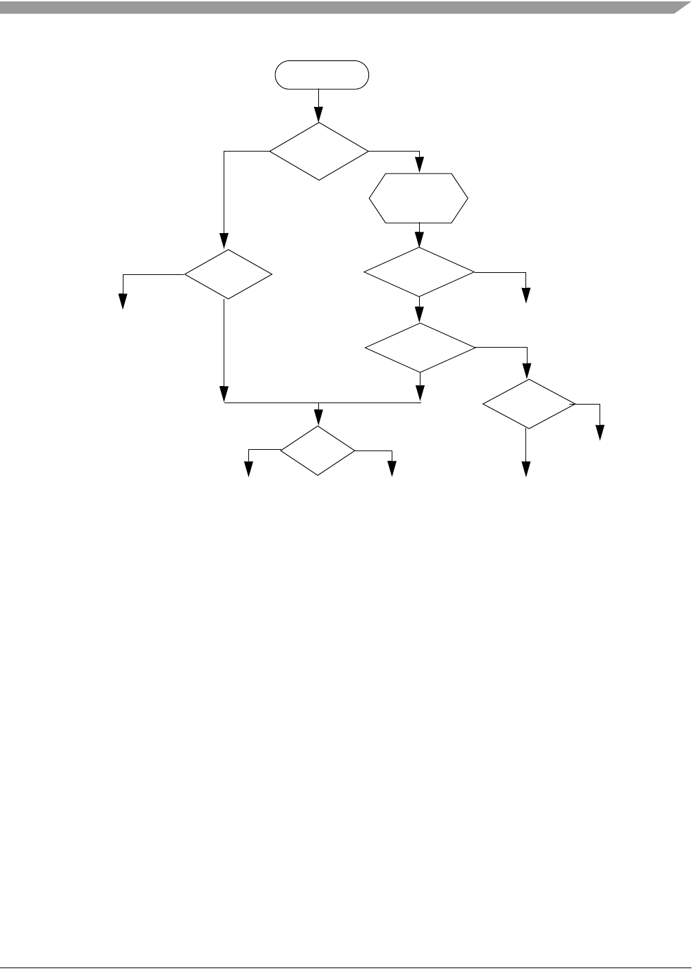
Functional Description
MCF548x Reference Manual, Rev. 3
Freescale Semiconductor 30-49
Figure 30-41. Ethernet Address Recognition—Receive Block Decisions
30.4.7 Hash Algorithm
The hash table algorithm used in the group and individual hash filtering operates as follows. The 48-bit
destination address is mapped into one of 64 bits, which are represented by 64 bits stored in GAUR, GALR
(group address hash match) or IAUR, IALR (individual address hash match). This mapping is performed
by passing the 48-bit address through the FEC’s 32-bit CRC generator and selecting the 6 most significant
bits of the CRC-encoded result to generate a number between 0 and 63. The MSB of the CRC result selects
GAUR (MSB = 1) or GALR (MSB = 0). The least significant 5 bits of the hash result select the bit within
the selected register. If the CRC generator selects a bit that is set in the hash table, the frame is accepted;
otherwise, it is rejected.
For example, if eight group addresses are stored in the hash table and random group addresses are received,
the hash table prevents roughly 56/64 (or 87.5%) of the group address frames from reaching memory.
Those that do reach memory must be further filtered by the processor to determine if they truly contain
one of the eight desired addresses.
The effectiveness of the hash table declines as the number of addresses increases.
Accept/Reject
Broadcast Addr
?
?
PROM = 1
?
Receive
Address
True
NOTES:
BC_REJ - field in RCR register (BroadCast REJect)
False
True
False BC_REJ = 1
?
Frame
Hash Match
?
Exact Match
?
Pause Frame
False
False
False
False
True
True
True
True
Receive Frame Receive Frame
Receive Frame Receive Frame
Reject Frame
Reject Frame
PROM - field in RCR register (PROMiscous mode)
Pause Frame - valid PAUSE frame received
Set BC bit in Rcv BD Set MC bit in RFSW if multicast
Set M (Miss) bit in Rcv BD
Set MC bit in Rcv BD if multicast
Set BC bit in Rcv BD if broadcast
Recognition

MCF548x Reference Manual, Rev. 3
30-50 Freescale Semiconductor
The hash table registers must be initialized by the user. The CRC32 polynomial to use in computing the
hash is:
Eqn. 30-1
A table of example destination addresses and corresponding hash values is included below for reference.
Table 30-49. Destination Address to 6-Bit Hash
48-bit Destination
Address
6-bit Hash (in
Hex)
Hash Decimal
Value
65:FF:FF:FF:FF:FF 0x0 0
55:FF:FF:FF:FF:FF 0x1 1
15:FF:FF:FF:FF:FF 0x2 2
35:FF:FF:FF:FF:FF 0x3 3
B5:FF:FF:FF:FF:FF 0x4 4
95:FF:FF:FF:FF:FF 0x5 5
D5:FF:FF:FF:FF:FF 0x6 6
F5:FF:FF:FF:FF:FF 0x7 7
DB:FF:FF:FF:FF:FF 0x8 8
FB:FF:FF:FF:FF:FF 0x9 9
BB:FF:FF:FF:FF:FF 0xA 10
8B:FF:FF:FF:FF:FF 0xB 11
0B:FF:FF:FF:FF:FF 0xC 12
3B:FF:FF:FF:FF:FF 0xD 13
7B:FF:FF:FF:FF:FF 0xE 14
5B:FF:FF:FF:FF:FF 0xF 15
27:FF:FF:FF:FF:FF 0x10 16
07:FF:FF:FF:FF:FF 0x11 17
57:FF:FF:FF:FF:FF 0x12 18
77:FF:FF:FF:FF:FF 0x13 19
F7:FF:FF:FF:FF:FF 0x14 20
C7:FF:FF:FF:FF:FF 0x15 21
97:FF:FF:FF:FF:FF 0x16 22
A7:FF:FF:FF:FF:FF 0x17 23
99:FF:FF:FF:FF:FF 0x18 24
B9:FF:FF:FF:FF:FF 0x19 25
F9:FF:FF:FF:FF:FF 0x1A 26
C9:FF:FF:FF:FF:FF 0x1B 27
x32 x26 x23 x22 x16 x12 x11 x10 x8x7x5x4x2x1+ + + + + + + +++++++

Functional Description
MCF548x Reference Manual, Rev. 3
Freescale Semiconductor 30-51
59:FF:FF:FF:FF:FF 0x1C 28
79:FF:FF:FF:FF:FF 0x1D 29
29:FF:FF:FF:FF:FF 0x1E 30
19:FF:FF:FF:FF:FF 0x1F 31
D1:FF:FF:FF:FF:FF 0x20 32
F1:FF:FF:FF:FF:FF 0x21 33
B1:FF:FF:FF:FF:FF 0x22 34
91:FF:FF:FF:FF:FF 0x23 35
11:FF:FF:FF:FF:FF 0x24 36
31:FF:FF:FF:FF:FF 0x25 37
71:FF:FF:FF:FF:FF 0x26 38
51:FF:FF:FF:FF:FF 0x27 39
7F:FF:FF:FF:FF:FF 0x28 40
4F:FF:FF:FF:FF:FF 0x29 41
1F:FF:FF:FF:FF:FF 0x2A 42
3F:FF:FF:FF:FF:FF 0x2B 43
BF:FF:FF:FF:FF:FF 0x2C 44
9F:FF:FF:FF:FF:FF 0x2D 45
DF:FF:FF:FF:FF:FF 0x2E 46
EF:FF:FF:FF:FF:FF 0x2F 47
93:FF:FF:FF:FF:FF 0x30 48
B3:FF:FF:FF:FF:FF 0x31 49
F3:FF:FF:FF:FF:FF 0x32 50
D3:FF:FF:FF:FF:FF 0x33 51
53:FF:FF:FF:FF:FF 0x34 52
73:FF:FF:FF:FF:FF 0x35 53
23:FF:FF:FF:FF:FF 0x36 54
13:FF:FF:FF:FF:FF 0x37 55
3D:FF:FF:FF:FF:FF 0x38 56
0D:FF:FF:FF:FF:FF 0x39 57
5D:FF:FF:FF:FF:FF 0x3A 58
7D:FF:FF:FF:FF:FF 0x3B 59
Table 30-49. Destination Address to 6-Bit Hash (Continued)
48-bit Destination
Address
6-bit Hash (in
Hex)
Hash Decimal
Value

MCF548x Reference Manual, Rev. 3
30-52 Freescale Semiconductor
30.4.8 Full Duplex Flow Control
Full-duplex flow control allows the user to transmit pause frames and to detect received pause frames.
Upon detection of a pause frame, MAC data frame transmission stops for a given pause duration.
To enable pause frame detection, the FEC must operate in full-duplex mode (TCR[FDEN] asserted) and
flow control enable (RCR[FCE]) must be asserted. The FEC detects a pause frame when the fields of the
incoming frame match the pause frame specifications, as shown in the table below. In addition, the receive
status associated with the frame should indicate that the frame is valid.
Pause frame detection is performed by the receive module. The FEC runs an address recognition
subroutine to detect the specified pause frame destination address, while the receiver detects the type and
opcode pause frame fields. On detection of a pause frame, TCR[GTS] is asserted by the FEC internally.
When transmission has paused, the EIR[GRA] interrupt is asserted and the pause timer begins to
increment. The pause timer increments once every slot time ( 512 bit times ), until OPD[PAUSE_DUR]
slot times have expired. On OPD[PAUSE_DUR] expiration, TCR[GTS] is deasserted allowing MAC data
frame transmission to resume. Note that the receive flow control pause (TCR[RFC_PAUSE]) status bit is
asserted while the transmitter is paused due to reception of a pause frame.
To transmit a pause frame, the FEC must operate in full-duplex mode and the user must assert flow control
pause (TCR[TFC_PAUSE]). On assertion of transmit flow control pause (TCR[TFC_PAUSE]), the
transmitter asserts TCR[GTS] internally. When the transmission of data frames stops, the EIR[GRA]
(graceful stop complete) interrupt asserts. Following EIR[GRA] assertion, the pause frame is transmitted.
On completion of pause frame transmission, flow control pause (TCR[TFC_PAUSE]) and TCR[GTS] are
deasserted internally.
During pause frame transmission, the transmit hardware places data into the transmit data stream from the
registers shown in the table below.
FD:FF:FF:FF:FF:FF 0x3C 60
DD:FF:FF:FF:FF:FF 0x3D 61
9D:FF:FF:FF:FF:FF 0x3E 62
BD:FF:FF:FF:FF:FF 0x3F 63
Table 30-50. PAUSE Frame Field Specification
PAUSE Frame Fields Register Contents
48-bit Destination Address 01:80:C2:00:00:01 or Physical Address
48-bit Source Address Any
16-bit Type 0x8808
16-bit Opcode 0x0001
16-bit PAUSE Duration 0x0000 to 0xFFFF
Table 30-49. Destination Address to 6-Bit Hash (Continued)
48-bit Destination
Address
6-bit Hash (in
Hex)
Hash Decimal
Value

Functional Description
MCF548x Reference Manual, Rev. 3
Freescale Semiconductor 30-53
The user must specify the desired pause duration in the OPD register.
Note that when the transmitter is paused due to receiver/microcontroller pause frame detection, transmit
flow control pause (TCR[TFC_PAUSE]) still may be asserted and will cause the transmission of a single
pause frame. In this case, the EIR[GRA] interrupt will not be asserted.
30.4.9 Inter-Packet Gap (IPG) Time
The minimum inter-packet gap time for back-to-back transmission is 96 bit times. After completing a
transmission or after the backoff algorithm completes, the transmitter waits for carrier sense to be negated
before starting its 96 bit time IPG counter. Frame transmission may begin 96 bit times after carrier sense
is negated if it stays negated for at least 60 bit times. If carrier sense asserts during the last 36 bit times, it
will be ignored and a collision will occur.
The receiver receives back-to-back frames with a minimum spacing of at least 28 bit times. If an IPG
between receive frames is less than 28 bit times, the following frame may be discarded by the receiver.
30.4.10 Collision Handling
If a collision occurs during frame transmission, the Ethernet controller will continue the transmission for
at least 32 bit times, transmitting a JAM pattern consisting of 32 ones. If the collision occurs during the
preamble sequence, the JAM pattern will be sent after the end of the preamble sequence.
If a collision occurs within 512 bit times, the retry process is initiated. The transmitter waits a random
number of slot times. A slot time is 512 bit times. If a collision occurs after 512 bit times, then no
retransmission is performed and the EIR[LC] bit is set.
30.4.11 Internal and External Loopback
Both internal and external loopback are supported by the Ethernet controller. In loopback mode, both of
the FIFOs are used and the FEC actually operates in a full-duplex fashion. Both internal and external
loopback are configured using combinations of the LOOP and DRT bits in the RCR register and the FDEN
bit in the TCR register.
For both internal and external loopback set FDEN = 1.
For internal loopback set RCR[LOOP] = 1 and RCR[DRT] = 0. ETXEN and ETXER will not assert during
internal loopback. During internal loopback, the transmit/receive data rate is higher than in normal
operation because the internal system clock is used by the transmit and receive blocks instead of the clocks
from the external transceiver. This will cause an increase in the required system bus bandwidth for transmit
and receive data being DMA’d to/from external memory. It may be necessary to pace the frames on the
Table 30-51. Transmit Pause Frame Registers
PAUSE Frame Fields FEC Register Register Contents
48-bit destination address Internal 0x0180_C200_0001
48-bit Source Address {PALR[31:0], PAHR[31:16]} Physical Address
16-bit type PAHR[15:0] 0x8808
16-bit opcode OPD[31:16] 0x0001
16-bit PAUSE duration OPD[15:0] 0x0000 to 0xFFFF

MCF548x Reference Manual, Rev. 3
30-54 Freescale Semiconductor
transmit side and/or limit the size of the frames to prevent transmit FIFO underrun and receive FIFO
overflow.
For external loopback set RCR[LOOP] = 0, RCR[DRT] = 0 and configure the external transceiver for
loopback.
30.4.12 Ethernet Error-Handling Procedure
The Ethernet controller reports frame reception and transmission error conditions using the receive frame
status words (RFSWs), the EIR register, and the MIB block counters.
30.4.12.1 Transmission Errors
30.4.12.1.1 Transmitter Underrun
If this error occurs, the FEC sends 32 bits that ensure a CRC error and stops transmitting. The XFUN bit
is set in the EIR. The FEC will then continue to the next transmit buffer descriptor and begin transmitting
the next frame.
The XFUN interrupt will be asserted if enabled in the EIMR register.
30.4.12.1.2 Retransmission Attempts Limit Expired
When this error occurs, the FEC terminates transmission. The RL bit is set in the EIR. The FEC will then
begin transmitting the next frame.
The “RL” interrupt will be asserted if enabled in the EIMR register.
30.4.12.1.3 Late Collision
When a collision occurs after the slot time (512 bits starting at the Preamble), the FEC terminates
transmission. All remaining data in the frame is discarded, and the LC bit is set in the EIR register. The
FEC will then continue to the next transmit buffer descriptor and begin transmitting the next frame.
The “LC” interrupt will be asserted if enabled in the EIMR register.
30.4.12.1.4 Heartbeat
Some transceivers have a self-test feature called “heartbeat” or “signal quality error.” To signify a good
self-test, the transceiver indicates a collision to the FEC within 4 microseconds after completion of a frame
transmitted by the Ethernet controller. This indication of a collision does not imply a real collision error
on the network, but is rather an indication that the transceiver still seems to be functioning properly. This
is called the heartbeat condition.
If the HBC bit is set in the TCR register and the heartbeat condition is not detected by the FEC after a
frame transmission, then a heartbeat error occurs. When this error occurs, the FEC generates the HBERR
interrupt if it is enabled.

Functional Description
MCF548x Reference Manual, Rev. 3
Freescale Semiconductor 30-55
30.4.12.2 Reception Errors
30.4.12.2.1 Overrun Error
If the receive block has data to put into the receive FIFO and the receive FIFO is full, the FEC sets the OV
bit in the receive frame status word (RFSW). All subsequent data in the frame will be discarded and
subsequent frames may also be discarded until the receive FIFO is serviced by the DMA and space is made
available. At this point the RFSW is written into the FIFO with the OV bit set. This frame must be
discarded by the driver.
30.4.12.2.2 Non-Octet Error (Dribbling Bits)
The Ethernet controller handles up to seven dribbling bits when the receive frame terminates past a
non-octet aligned boundary. Dribbling bits are not used in the CRC calculation. If there is a CRC error,
then the frame non-octet aligned (NO) error is reported in the RFSW. If there is no CRC error, then no error
is reported.
30.4.12.2.3 CRC Error
When a CRC error occurs with no dribble bits, the FEC closes the buffer and sets the CR bit in the RFSW.
CRC checking cannot be disabled, but the CRC error can be ignored if checking is not required.
30.4.12.2.4 Frame Length Violation
When the receive frame length exceeds MAX_FL bytes the BABR interrupt will be generated, and the LG
bit in the RFSW will be set. The frame is not truncated unless the frame length exceeds 2047 bytes).
30.4.12.2.5 Truncation
When the receive frame length exceeds 2047 bytes the frame is truncated and the TR bit is set in the RFSW.
30.4.13 MII Data Frame
Ethernet/802.3 data frames transmitted across the MII have the following format:
<inter-frame><preamble><sfd><data><efd>
The inter-frame period is an unspecified amount of time during which no data activity occurs on the MII.
The de-assertion of ERXDV and ETXEN indicate the absence of data activity.
The preamble begins a frame and has a bit value of the following:
10101010 10101010 10101010 10101010 10101010 10101010 10101010
The left-most 1 represents the LSB of the byte.
The start of frame delimiter (sfd) represents the start of a frame and has the bit value, 10101011.

MCF548x Reference Manual, Rev. 3
30-56 Freescale Semiconductor
The data portion of the frame consists of N octets which corresponds to 2N nibbles being transmitted. The
order of each nibble is defined in the figure below.
Figure 30-42. MII Nibble/Octet to Octet/Nibble Mapping
The End-of-Frame delimiter is indicated by the de-assertion of the ETXEN signal for data on ETXD. For
data on ERXD, the de-assertion of ERXDV constitutes an End-of-Frame delimiter.
30.4.14 MII Management Frame Structure
A transceiver management frame being transmitted on the MII management interface uses the EMDIO and
EMDC signals. A transaction or frame on this serial interface has the following format:
<preamble><st><op><phyad><regad><ta><data><idle>
The (optional) preamble consists of a sequence of 32 continuous logic 1’s.
The start of frame (st), is indicated by a <01> pattern.
The operation code (op) for a read instruction is <10>. For a write operation, the operation code is <01>.
The physical address (phyad) is a five bit field which allows for up to 32 PHYs to be addressed. The first
address bit transmitted is the MSB of the address.
The register address (regad) is a five bit field which allows for 32 registers to be addressed within the each
PHY. The first register bit transmitted is the MSB of the address.
The turnaround (ta) field is a two bit field which provides spacing between the register address field and
the data field to avoid contention on the EMDIO signal during a read operation.
The data field is 16 bits wide. The first data bit transmitted and received is data bit 15.
During idle condition, EMDIO is in the high impedance state.
The MII management register set located in the PHY may consist of a basic register set and an extended
register set as defined below.
Table 30-52. MII Management Register Set
Register Addr. Register Name Basic/Extended
0 Control B
1Status B
2,3 PHY Identifier E
D0 D1 D2 D3 D4 D5 D6 D7
LSB MSBFirst Nibble Second Nibble
D0 D1 D2 D3
LSB MSB
First Bit
MII Nibble

Functional Description
MCF548x Reference Manual, Rev. 3
Freescale Semiconductor 30-57
4 Auto-Negotiation (AN)
Advertisement
E
5 AN Link Partner Ability E
6 AN Expansion E
7 AN Next Page Transmit E
8-15 Reserved E
16-31 Vendor Specific E
Table 30-52. MII Management Register Set (Continued)
Register Addr. Register Name Basic/Extended

MCF548x Reference Manual, Rev. 3
30-58 Freescale Semiconductor


MCF548x Reference Manual, Rev. 3
ii Freescale Semiconductor

MCF548x Reference Manual, Rev. 3
Freescale Semiconductor 31-1
Chapter 31
Mechanical Data
This chapter contains drawings showing the pinout, packaging, and mechanical characteristics of the
MCF548x. See the website http://www.freescale.com/coldfire for any updated information.
31.1 Package
The MCF548x is assembled in a 388-pin, thermally enhanced plastic BGA package.
31.2 Pinout
The MCF548x pinout is detailed in Table 31-1, including the primary and alternate functions of
multiplexed signals.
Table 31-1. MCF5485/MCF5484 Signal Description by Pin Number
PBGA
Pin
Pin Functions PBGA
Pin
Pin Functions
Primary GPIO Secondary Tertiary Primary GPIO Secondary Tertiary
A1 SDVDD — — — P1 SDCS1 ———
A2 VSS — — — P2 SDCS2 ———
A3 SDDM2 ———P3SD_VDD — — —
A4 SDDATA23 ———P4IVDD — — —
A5 SDDATA24 —— — P11 VSS — — —
A6 SDDATA27 —— — P12 VSS — — —
A7 SDDQS3 —— — P13 VSS — — —
A8 SDDATA29 —— — P14 VSS — — —
A9 SDADDR0 —— — P15 VSS — — —
A10 SDADDR3 —— — P16 VSS — — —
A11 SDADDR7 —— — P23 PCIAD19 — FBADDR19 —
A12 SDADDR11 —— — P24 PCIAD20 — FBADDR20 —
A13 SDADDR12 —— — P25 PCIAD18 — FBADDR18 —
A14 IRQ5 PIRQ5 CANRX1 — P26 PCIAD21 — FBADDR21 —
A15 DSI —TDI—R1FBCS5PFBCS5 — —
A16 TCK — — — R2 SDCS3 ———
A17 CLKIN — — — R3 EVDD — — —
A18 MTMOD1 — — — R4 VSS — — —
A19 PLLVDD — — — R11 VSS — — —
A20 RSTO — — — R12 VSS — — —
A21 PSTDDATA1 —— — R13 VSS — — —

MCF548x Reference Manual, Rev. 3
31-2 Freescale Semiconductor
A22 PSTDDATA3 —— — R14 VSS — — —
A23 PSTDDATA7 —— — R15 VSS — — —
A24 PCIBR0 PPCIBR0 TIN0 — R16 VSS — — —
A25 PCIBR2 PPCIBR2 TIN2 — R23 IVDD — — —
A261E1RXD1 PFEC1L5 —— R24 PCIAD24 — FBADDR24 —
B1 SDVDD — — — R25 PCIAD23 — FBADDR23 —
B2 VSS — — — R26 PCIAD22 — FBADDR22 —
B3 SDDATA18 ———T1FBCS2PFBCS2 — —
B4 SDDATA20 ———T2FBCS4PFBCS4 — —
B5 SDDQS2 ———T3FBCS3PFBCS3 — —
B6 SDDATA21 ———T4 AD1 — — —
B7 SDDATA25 —— — T11 VSS — — —
B8 SDDM3 —— — T12 VSS — — —
B9 SDDATA30 —— — T13 VSS — — —
B10 SDADDR1 —— — T14 VSS — — —
B11 SDADDR5 —— — T15 VSS — — —
B12 SDADDR9 —— — T16 VSS — — —
B13 RSTI —— — T23 VSS — — —
B14 IRQ6 PIRQ6 CANRX1 — T24 PCIAD27 — FBADDR27 —
B15 BKPT — TMS — T25 PCIAD26 — FBADDR26 —
B16 MTMOD0 —— — T26 PCIAD25 — FBADDR25 —
B17 MTMOD3 ———U1FBCS0 ———
B18 PLLVSS ———U2FBCS1PFBCS1 — —
B19 PSTDDATA0 ———U3 AD0 — — —
B20 PSTDDATA2 —— — U4 VSS — — —
B21 PSTDDATA6 —— — U23 VSS — — —
B221E1RXCLK PFEC1H3 —— U24 EVDD — — —
B23 PCIBR1 PPCIBR1 TIN1 — U25 PCIAD29 — FBADDR29 —
B24 PCIBR3 PPCIBR3 TIN3 — U26 PCIAD28 — FBADDR28 —
B251E1RXDV PFEC1H2 ——V1 AD3 — — —
B261E1RXD2 PFEC1L2 ——V2 AD2 — — —
Table 31-1. MCF5485/MCF5484 Signal Description by Pin Number (Continued)
PBGA
Pin
Pin Functions PBGA
Pin
Pin Functions
Primary GPIO Secondary Tertiary Primary GPIO Secondary Tertiary

Pinout
MCF548x Reference Manual, Rev. 3
Freescale Semiconductor 31-3
C1 SDVDD —— — V3 AD4 — — —
C2 CAS ———V4IVDD — — —
C3 VSS —— — V23 DSPICS3 PDSPI5 TOUT3 CANTX1
C4 SDDATA17 —— — V24 PCIBG1 PPCIBG1 TOUT1 —
C5 SDDATA19 —— — V25 PCIAD31 — FBADDR31 —
C6 SDVDD —— — V26 PCIAD30 — FBADDR30 —
C7 SDDATA22 ———W1AD6 — — —
C8 SDDATA26 ———W2AD5 — — —
C9 SDVDD ———W3AD7 — — —
C10 SDDATA31 ———W4AD13 — — —
C11 SDADDR4 —— — W23 DSPICS5/PCSS PDSPI6 — —
C12 SDADDR8 ———W24PCIBG4PPCIBG4 TBST —
C13 SDVDD ———W25PCIBG2PPCIBG2 TOUT2 —
C14 MTMOD2 ———W26PCIBG0PPCIBG0 TOUT0 —
C15 DSCLK —TRST—Y1 AD9 — — —
C16 EVDD —— — Y2 AD8 — — —
C17 VSS —— — Y3 EVDD — — —
C18 IVDD —— — Y4 VSS — — —
C19 VSS — — — Y23 PSC1RTS PPSC1PSC06 PSC1FSYNC —
C20 PSTDDATA4 —— — Y24 DSPISOUT PDSPI0 PSC3TXD —
C21 VSS —— — Y25 DSPICS0/SS PDSPI3 — —
C22 EVDD —— — Y26 PCIBG3 PPCIBG3 TOUT3 —
C23 PCIIDSEL —— — AA1 AD10 — — —
C24 SDA PFECI2C1 — — AA2 AD11 — — —
C25 SCL PFECI2C0 — — AA3 AD14 — — —
C26 PCITRDY —— — AA4 AD19 — — —
D1 SDDATA14 —— — AA23 IVDD — — —
D2 VREF —— — AA24 EVDD — — —
D3 SDVDD —— — AA25 PCS0TXD PPSC1PSC00 — —
D4 SDDATA16 —— — AA26 DSPICS2 PDSPI4 TOUT2 CANTX1
D5 SDDATA28 —— — AB1 AD12 — — —
Table 31-1. MCF5485/MCF5484 Signal Description by Pin Number (Continued)
PBGA
Pin
Pin Functions PBGA
Pin
Pin Functions
Primary GPIO Secondary Tertiary Primary GPIO Secondary Tertiary

MCF548x Reference Manual, Rev. 3
31-4 Freescale Semiconductor
D6 VSS —— — AB2 AD15 — — —
D7 SDADDR2 —— — AB3 EVDD — — —
D8 SDADDR6 —— — AB4 VSS — — —
D9 VSS — — — AB23 PSC3RTS PPSC3PSC26 PSC3FSYNC —
D10 SDADDR10 —— — AB24 DACK0 PDMA2 TOUT0 —
D11 IVDD —— — AB25 PSC1TXD PPSC1PSC04 — —
D12 IVDD — — — AB26 PSC0RTS PPSC1PSC02 PSC0FSYNC —
D13 VSS ———AC1AD17 — — —
D14 IRQ7 PIRQ7 ——AC2AD20 — — —
D15 NC ———AC3AD22 — — —
D16 VSS ———AC4BE/BWE1 PFBCTL5 FBADDR1 —
D17 DSO —TDO—AC51E1CRS PFEC1H0 — —
D18 PSTDDATA5 ———AC6E0TXD2PFEC0L6— —
D19 IVDD —— — AC7 VSS — — —
D20 PSTCLK ———AC81E1TXD3 PFEC1L7 — —
D21 PCIBR4 PPCIBR4 IRQ4 — AC9 E0COL PFEC0H4 — —
D22 IVDD —— — AC10 VSS — — —
D23 VSS ———AC111E1TXD2 PFEC1L6 — —
D24 PCIIRDY ———AC12IVDD — — —
D251E1RXD31PFEC1L3 — — AC132USB_OSCVDD — — —
D26 PCIPERR —— — AC14 E0RXER PFEC0L0 — —
E1 SDDATA12 ———AC15 NC — — —
E2 SDDATA15 ———AC162USB_PHYVDD — — —
E3 RAS ———AC173USBVBUS — — —
E4 SDCKE —— — AC18 VSS — — —
E23 VSS —— — AC19 PSC2CTS PPSC3PSC23 PSC2BCLK CANRX0
E24 EVDD ———AC20IVDD — — —
E25 PCISTOP —— — AC21 PSC0RXD PPSC1PSC01 — —
E26 PCICXBE1 —— — AC22 TOUT2 PTIM4 CANTX1 —
F1 SDDATA10 ———AC23TOUT1 — — —
F2 SDDQS1 —— — AC24 DSPISIN PDSPI1 PSC3RXD —
Table 31-1. MCF5485/MCF5484 Signal Description by Pin Number (Continued)
PBGA
Pin
Pin Functions PBGA
Pin
Pin Functions
Primary GPIO Secondary Tertiary Primary GPIO Secondary Tertiary

Pinout
MCF548x Reference Manual, Rev. 3
Freescale Semiconductor 31-5
F3 SDVDD ———AC25DACK1 PDMA3 TOUT1 —
F4 VSS —— — AC26 PSC2TXD PPSC3PSC20 — —
F23 PCIPAR ———AD1AD16 — — —
F24 PCISERR ———AD2AD21 — — —
F25 PCIFRM ———AD3AD23 — — —
F26 PCICXBE3 ———AD4AD24 — — —
G1 SDDATA6 ———AD5AD26 — — —
G2 SDDATA9 —— — AD6 ALE PFBCTL0 TBST —
G3 SDDM1 —— — AD7 EVDD — — —
G4 SDDATA13 —— — AD8 E0TXD3 PFEC0L7 — —
G23 PCIRESET —— — AD9 E0TXD0 PFEC0H5 — —
G24 PCICXBE0 —— — AD10 EVDD — — —
G25 PCICXBE2 —— — AD11 E0MDC PFECI2C2 — —
G26 PCIAD2 — FBADDR2 — AD12 VSS ———
H1 SDDQS0 —— — AD13 E0RXD0 PFEC0H1 — —
H2 SDDATA5 —— — AD14 E0RXLK PFEC0H3 — —
H3 SDDATA8 ———AD152USB_OSCAVDD — — —
H4 IVDD ———AD162USB_PLLVDD — — —
H23 IVDD —— — AD17 VSS — — —
H24 EVDD —— — AD18 EVDD — — —
H25 PCIAD1 — FBADDR1 — AD19 TIN3 PTIM3 IRQ3 CANRX1
H26 PCIAD4 — FBADDR4 — AD20 VSS — — —
J1 SDDATA3 —— — AD21 PSC2RXD PPSCH1 — —
J2 SDDM0 —— — AD22 DSPISCK PDSPI2 PSC3CTS PSC3BCLK
J3 SDDATA4 —— — AD23 TOUT3 PTIM6 CANTX1 —
J4 VSS ———AD241E1MDC —SCL CANTX0
J23 PCIDEVSEL ———AD251E1TXEN PFEC1H6 — —
J24 PCIAD3 — FBADDR3 — AD26 PSC2RTS PPSC3PSC22 PSC2FSYNC CANTX0
J25 PCIAD5 — FBADDR5 — AE1 AD18 — — —
J26 PCIAD7 — FBADDR7 — AE2 AD31 — — —
K1 SDWE —— — AE3 AD28 — — —
Table 31-1. MCF5485/MCF5484 Signal Description by Pin Number (Continued)
PBGA
Pin
Pin Functions PBGA
Pin
Pin Functions
Primary GPIO Secondary Tertiary Primary GPIO Secondary Tertiary

MCF548x Reference Manual, Rev. 3
31-6 Freescale Semiconductor
K2 SDDATA0 —— — AE4 AD27 — — —
K3 SDDATA1 —— — AE5 R/W PFBCTL2 TBST —
K4 SDDATA11 —— — AE6 OE PFBCTL3 — —
K23 PCIAD0 — FBADDR0 — AE7 BE/BWE0 PFBCTL4 FBADDR0 —
K24 PCIAD6 — FBADDR6 — AE81E1RXER PFEC1L0 — —
K25 PCIAD8 — FBADDR8 — AE9 E0TXER PFEC0L4 — —
K26 PCIAD9 — FBADDR9 — AE10 E0TXEN PFEC0H6 — —
L1 SDCLK1 ———AE111E1TXD1 PFEC1L5 — —
L2 SDRDQS ———AE121E1TXD0 PFEC1h5 — —
L3 SDVDD ———AE131E1TXCLK PFEC1H7 — —
L4 VSS —— — AE14 E0RXDV PFEC1H2 — —
L11 VSS —— — AE15 VSS — — —
L12 VSS —— — AE16 VSS — — —
L13 VSS —— — AE17 VSS — — —
L14 VSS ———AE182USBVDD — — —
L15 VSS —— — AE19 E0CRS PFEC0H0 — —
L16 VSS —— — AE20 TIN1 — — —
L23 IVDD —— — AE21 PSC3RXD PPSC3PSC25 — —
L24 VSS —— — AE22 PSC1RXD PPSC1PSC05 — —
L25 PCIAD10 — FBADDR10 — AE23 PSC0CTS PPSC1PSC03 PSC0BCLK —
L26 PCIAD11 — FBADDR11 — AE241E1TXER PFEC1L4 — —
M1 SDCLK1 — ——AE251E1MDIO —SCL CANTX0
M2 SDBA1 —— — AE26 PSC3TXD PPSC3PSC24 — —
M3 SDBA0 ———AF1AD29 — — —
M4 SDDATA2 ———AF2AD25 ———
M11 VSS ———AF3AD30 — — —
M12 VSS —— — AF4 BE/BWE3 PFBCTL7 TSIZ1 —
M13 VSS —— — AF5 BE/BWE2 PFBCTL6 TSIZ0 —
M14 VSS ———AF6 TA PFBCTL1 — —
M15 VSS —— — AF7 E0TXD1 PFEC0L5 — —
M16 VSS ———AF81E1COL PFEC1H4 — —
Table 31-1. MCF5485/MCF5484 Signal Description by Pin Number (Continued)
PBGA
Pin
Pin Functions PBGA
Pin
Pin Functions
Primary GPIO Secondary Tertiary Primary GPIO Secondary Tertiary

Pinout
MCF548x Reference Manual, Rev. 3
Freescale Semiconductor 31-7
M23 VSS —— — AF9 E0TXCLK PFEC0H7 — —
M24 EVDD —— — AF10 E0MDIO PFECI2C3 — —
M25 PCIAD12 — FBADDR12 — AF11 E0RXD3 PFEC0L3 — —
M26 PCIAD13 — FBADDR13 — AF12 E0RXD2 PFEC0L2 — —
N1 SDCLK0 —— — AF13 E0RXD1 PFEC0L1 — —
N2 SDCLK0 ———AF143USBCLKOUT — — —
N3 SDCS0 ———AF153USBCLKIN — — —
N4 SDDATA7 ———AF163USBD+ — — —
N11 VSS ———AF173USBD- — — —
N12 VSS ———AF18 USBRBIAS — — —
N13 VSS —— — AF19 DREQ1 PDMA1 TIN1 IRQ1
N14 VSS —— — AF20 DREQ0 PDMA0 TIN0 —
N15 VSS ———AF21TIN2 PTIM5 IRQ2 CANRX1
N16 VSS ———AF22TIN0 ———
N23 PCIAD16 — FBADDR16 — AF23 PSC3CTS PPSC3PSC27 PSC3BCLK —
N24 PCIAD14 — FBADDR14 — AF241E1RXD0 PFEC1H1 — —
N25 PCIAD17 — FBADDR17 — AF25 PSC1CTS PPSC1PSC07 PSC1BCLK —
N26 PCIAD15 — FBADDR15 — AF26 TOUT0 — — —
1This pin is a “no connect” on the MCF5483 and MCF5482 devices.
2This pin is a “no connect” on the MCF5481 and MCF5480 devices. On MCF5485, MCF5484, MCF5483, and MCF5482 device
the pin should be connected to the appriopriate power rail even is USB is not being used.
3This pin is a “no connect” on the MCF5481 and MCF5480 devices.
Table 31-1. MCF5485/MCF5484 Signal Description by Pin Number (Continued)
PBGA
Pin
Pin Functions PBGA
Pin
Pin Functions
Primary GPIO Secondary Tertiary Primary GPIO Secondary Tertiary

MCF548x Reference Manual, Rev. 3
31-8 Freescale Semiconductor
31.3 Mechanical Diagrams
31.3.1 MCF5485/5484 Mechanical Diagram
Figure 31-1–Figure 31-4 show the pinout for the each quadrant of the MCF5485/MCF5484 388 PBGA
package. Figure 31-1 shows the pinout for the upper left quadrant.
Figure 31-1. MCF5485/5484 Upper Left Quadrant Pinout (388 PBGA)
12345678910111213
A
SDVDD VSS SDDM2 SDDAT
A23
SDDAT
A24
SDDAT
A27
SDDQS
3
SDDAT
A29
SDADD
R0
SDADD
R3
SDADD
R7
SDADD
R11
SDADD
R12
B
SDVDD VSS SDDDA
TA18
SDDAT
A20
SDDQS
2
SDDAT
A21
SDDAT
A25
SDDM3 SDDAT
A30
SDADD
R1
SDADD
R5
SDADD
R9
RSTI
C
SDVDD CAS VSS SDDAT
A17
SDDAT
A19
SDVDD SDDAT
A22
SDDAT
A26
SDVDD SDDAT
A31
SDADD
R4
SDADD
R8
SDVDD
D
SDDAT
A14
VREF SDVDD SDDAT
A16
SDDAT
A28
VSS SDADD
R2
SDADD
R6
VSS SDADD
R10
IVDD IVDD VSS
E
SDDAT
A12
SDDAT
A15
RAS SDCKE
F
SDDDA
TA1 0
SDDQS
1
SDVDD VSS
G
SDDAT
A6
SDDAT
A9
SDDM1 SDDAT
A13
H
SDDQS
0
SDDAT
A5
SDDAT
A8
IVDD
J
SDDAT
A3
SDDM0 SDDAT
A4
VSS
K
SDWE SDDAT
A0
SDDAT
A1
SDDAT
A11
L
SDCLK
1
SDRDQ
S
SDVDD VSS VSS VSS VSS
M
SDCLK
1
SDBA1 SDBA0 SDDAT
A2
VSS VSS VSS
N
SDCLK
0
SDCLK
0
SDCS0 SDDAT
A7
VSS VSS VSS

Mechanical Diagrams
MCF548x Reference Manual, Rev. 3
Freescale Semiconductor 31-9
Figure 31-2 shows the pinout for the upper right quadrant of the MCF5485/MCF5484 pinout for the 388
PBGA package.
Figure 31-2. MCF5485/5484 Upper Right Quadrant Pinout (388 PBGA)
14 15 16 17 18 19 20 21 22 23 24 25 26
A
IRQ5 DSI/TDI TCK CLKIN MTMOD
1
PLLVDD RSTO PSTDD
ATA1
PSTDD
ATA3
PSTDD
ATA7
PCIBR0 PCIBR2 E1RXD
1
B
IRQ6 BKPT/T
MS
MTMOD
0
MTMOD
3
PLLVSS PSTDD
ATA0
PSTDD
ATA2
PSTDD
ATA6
E1RXC
LK
PCIBR1 PCIBR3 E1RXD
V
E1RXD
2
C
MTMOD
2
DSCLK/
TRST
EVDD VSS IVDD VSS PSTDD
ATA4
VSS EVDD PCIIDS
EL
SDA SCL PCITRD
Y
D
IRQ7 NC VSS DSO/TD
O
PSTDD
ATA5
IVDD PSTCL
K
PCIBR4 IVDD VSS PCIIRD
Y
E1RXD
3
PCIPER
R
E
VSS EVDD PCISTO
P
PCICXB
E1
F
PCIPAR PCISER
R
PCIFR
M
PCICXB
E3
G
PCIRES
ET
PCICXB
E0
PCICXB
E2
PCIAD2
H
IVDD EVDD PCIAD1 PCIAD4
J
PCIDEV
SEL
PCIAD3 PCIAD5 PCIAD7
K
PCIAD0 PCIAD6 PCIAD8 PCIAD9
L
VSS VSS VSS IVDD VSS PCIAD1
0
PCIAD1
1
M
VSS VSS VSS VSS EVDD PCIAD1
2
PCIAD1
3
N
VSS VSS VSS PCIAD1
6
PCIAD1
4
PCIAD1
7
PCIAD1
5

MCF548x Reference Manual, Rev. 3
31-10 Freescale Semiconductor
Figure 31-3 shows the pinout for the lower left quadrant of the MCF5485/MCF5484 pinout for the 388
PBGA package.
Figure 31-3. MCF5485/5484 Lower Left Quadrant Pinout (388 PBGA)
12345678910111213
P
SDCS1 SDCS2 SDVDD IVDD VSS VSS VSS
R
FBCS5 SDCS3 EVDD VSS VSS VSS VSS
T
FBCS2 FBCS4 FBCS3 AD1 VSS VSS VSS
U
FBCS0 FBCS1 AD0 VSS
V
AD3 AD2 AD4 IVDD
W
AD6 AD5 AD7 AD13
Y
AD9 AD8 EVDD VSS
AA
AD10 AD11 AD14 AD19
AB
AD12 AD15 EVDD VSS
AC
AD17 AD20 AD22 BE/BW
E1
E1CRS E0TXD
2
VSS E1TXD
3
E0COL VSS E1TXD
2
IVDD USB_OS
CVDD
AD
AD16 AD21 AD23 AD24 AD26 ALE EVDD E0TXD
3
E0TXD
0
EVDD E0MDC VSS E0RXD0
AE
AD18 AD31 AD28 AD27 R/W OE BE/BW
E0
E1RXE
R
E0TXE
R
E0TXE
N
E1TXD
1
E1TXD
0
E1TXCL
K
AF
AD29 AD25 AD30 BE/BW
E3
BE/BW
E2
TA E0TXD
1
E1COL E0TXC
LK
E0MDI
O
E0RXD
3
E0RXD
2
E0RXD1

Mechanical Diagrams
MCF548x Reference Manual, Rev. 3
Freescale Semiconductor 31-11
Figure 31-4 shows the pinout for the lower left quadrant of the MCF5485/MCF5484 pinout for the 388
PBGA package.
Figure 31-4. MCF5485/5484 Lower Right Quadrant Pinout (388 PBGA)
14 15 16 17 18 19 20 21 22 23 24 25 26
P
VSS VSS VSS PCIAD
19
PCIAD
20
PCIAD
18
PCIAD
21
R
VSS VSS VSS IVDD PCIAD
24
PCIAD
23
PCIAD
22
T
VSS VSS VSS VSS PCIAD
27
PCIAD
26
PCIAD
25
U
VSS EVDD PCIAD
29
PCIAD
28
V
DSPIC
S3
PCIBG
1
PCIAD
31
PCIAD
30
W
DSPIC
S5/PCS
S
PCIBG
4
PCIBG
2
PCIBG
0
Y
PSC1R
TS
DSPIS
OUT
DSPIC
S0/SS
PCIBG
3
AA
IVDD EVDD PSC0T
XD
DSPIC
S2
AB
PSC3R
TS
DACK0 PSC1T
XD
PSC0R
TS
AC
E0RXE
R
NC USB_P
HYVDD
USBVB
US
VSS PSC2C
TS
IVDD PSC0R
XD
TOUT2 TOUT1 DSPISI
N
DACK1 PSC2T
XD
AD
E0RXC
LK
USB_O
SCAVD
D
USB_P
LLVDD
VSS EVDD TIN3 VSS PSC2R
XD
DSPIS
CK
TOUT3 E1MDC E1TXE
N
PSC2R
TS
AE
E0RXD
V
VSS VSS VSS USBVD
D
E0CRS TIN1 PSC3R
XD
PSC1R
XD
PSC0C
TS
E1TXE
R
E1MDI
O
PSC3T
XD
AF
USBCL
KOUT
USBCL
KIN
USBD+ USBD- USBRB
IAS
DREQ1 DREQ0 TIN2 TIN0 PSC3C
TS
E1RXD
0
PSC1C
TS
TOUT0

MCF548x Reference Manual, Rev. 3
31-12 Freescale Semiconductor
31.3.2 MCF5483/5482 Mechanical Diagram
Figure 31-5–Figure 31-8 show the pinout for the each quadrant of the MCF5483/MCF5482 388 PBGA
package. Figure 31-5 shows the pinout for the upper left quadrant.
Figure 31-5. MCF5483/5482 Upper Left Quadrant Pinout (388 PBGA)
12345678910111213
A
SDVDD VSS SDDM2 SDDAT
A23
SDDAT
A24
SDDAT
A27
SDDQS
3
SDDAT
A29
SDADD
R0
SDADD
R3
SDADD
R7
SDADD
R11
SDADD
R12
B
SDVDD VSS SDDDA
TA18
SDDAT
A20
SDDQS
2
SDDAT
A21
SDDAT
A25
SDDM3 SDDAT
A30
SDADD
R1
SDADD
R5
SDADD
R9
RSTI
C
SDVDD CAS VSS SDDAT
A17
SDDAT
A19
SDVDD SDDAT
A22
SDDAT
A26
SDVDD SDDAT
A31
SDADD
R4
SDADD
R8
SDVDD
D
SDDAT
A14
VREF SDVDD SDDAT
A16
SDDAT
A28
VSS SDADD
R2
SDADD
R6
VSS SDADD
R10
IVDD IVDD VSS
E
SDDAT
A12
SDDAT
A15
RAS SDCKE
F
SDDDA
TA1 0
SDDQS
1
SDVDD VSS
G
SDDAT
A6
SDDAT
A9
SDDM1 SDDAT
A13
H
SDDQS
0
SDDAT
A5
SDDAT
A8
IVDD
J
SDDAT
A3
SDDM0 SDDAT
A4
VSS
K
SDWE SDDAT
A0
SDDAT
A1
SDDAT
A11
L
SDCLK
1
SDRDQ
S
SDVDD VSS VSS VSS VSS
M
SDCLK
1
SDBA1 SDBA0 SDDAT
A2
VSS VSS VSS
N
SDCLK
0
SDCLK
0
SDCS0 SDDAT
A7
VSS VSS VSS

Mechanical Diagrams
MCF548x Reference Manual, Rev. 3
Freescale Semiconductor 31-13
Figure 31-6 shows the pinout for the upper right quadrant of the MCF5483/MCF5482 pinout for the 388
PBGA package.
Figure 31-6. MCF5483/5482 Upper Right Quadrant Pinout (388 PBGA)
14 15 16 17 18 19 20 21 22 23 24 25 26
A
IRQ5 DSI/TDI TCK CLKIN MTMOD
1
PLLVDD RSTO PSTDD
ATA1
PSTDD
ATA3
PSTDD
ATA7
PCIBR0 PCIBR2 NC
B
IRQ6 BKPT/T
MS
MTMOD
0
MTMOD
3
PLLVSS PSTDD
ATA0
PSTDD
ATA2
PSTDD
ATA6
NC PCIBR1 PCIBR3 NC NC
C
MTMOD
2
DSCLK/
TRST
EVDD VSS IVDD VSS PSTDD
ATA4
VSS EVDD PCIIDS
EL
SDA SCL PCITRD
Y
D
IRQ7 NC VSS DSO/TD
O
PSTDD
ATA5
IVDD PSTCL
K
PCIBR4 IVDD VSS PCIIRD
Y
NC PCIPER
R
E
VSS EVDD PCISTO
P
PCICXB
E1
F
PCIPAR PCISER
R
PCIFR
M
PCICXB
E3
G
PCIRES
ET
PCICXB
E0
PCICXB
E2
PCIAD2
H
IVDD EVDD PCIAD1 PCIAD4
J
PCIDEV
SEL
PCIAD3 PCIAD5 PCIAD7
K
PCIAD0 PCIAD6 PCIAD8 PCIAD9
L
VSS VSS VSS IVDD VSS PCIAD1
0
PCIAD1
1
M
VSS VSS VSS VSS EVDD PCIAD1
2
PCIAD1
3
N
VSS VSS VSS PCIAD1
6
PCIAD1
4
PCIAD1
7
PCIAD1
5

MCF548x Reference Manual, Rev. 3
31-14 Freescale Semiconductor
Figure 31-7 shows the pinout for the lower left quadrant of the MCF5483/MCF5482 pinout for the 388
PBGA package.
Figure 31-7. MCF5483/5482 Lower Left Quadrant Pinout (388 PBGA)
12345678910111213
P
SDCS1 SDCS2 SDVDD IVDD VSS VSS VSS
R
FBCS5 SDCS3 EVDD VSS VSS VSS VSS
T
FBCS2 FBCS4 FBCS3 AD1 VSS VSS VSS
U
FBCS0 FBCS1 AD0 VSS
V
AD3 AD2 AD4 IVDD
W
AD6 AD5 AD7 AD13
Y
AD9 AD8 EVDD VSS
AA
AD10 AD11 AD14 AD19
AB
AD12 AD15 EVDD VSS
AC
AD17 AD20 AD22 BE/BW
E1
NC E0TXD
2
VSS NC E0COL VSS NC IVDD USB_OS
CVDD
AD
AD16 AD21 AD23 AD24 AD26 ALE EVDD E0TXD
3
E0TXD
0
EVDD E0MDC VSS E0RXD0
AE
AD18 AD31 AD28 AD27 R/W OE BE/BW
E0
NC E0TXE
R
E0TXE
N
NC NC NC
AF
AD29 AD25 AD30 BE/BW
E3
BE/BW
E2
TA E0TXD
1
NC E0TXC
LK
E0MDI
O
E0RXD
3
E0RXD
2
E0RXD1

Mechanical Diagrams
MCF548x Reference Manual, Rev. 3
Freescale Semiconductor 31-15
Figure 31-8 shows the pinout for the lower left quadrant of the MCF5483/MCF5482 pinout for the 388
PBGA package.
Figure 31-8. MCF5483/5482 Lower Right Quadrant Pinout (388 PBGA)
14 15 16 17 18 19 20 21 22 23 24 25 26
P
VSS VSS VSS PCIAD
19
PCIAD
20
PCIAD
18
PCIAD
21
R
VSS VSS VSS IVDD PCIAD
24
PCIAD
23
PCIAD
22
T
VSS VSS VSS VSS PCIAD
27
PCIAD
26
PCIAD
25
U
VSS EVDD PCIAD
29
PCIAD
28
V
DSPIC
S3
PCIBG
1
PCIAD
31
PCIAD
30
W
DSPIC
S5/PCS
S
PCIBG
4
PCIBG
2
PCIBG
0
Y
PSC1R
TS
DSPIS
OUT
DSPIC
S0/SS
PCIBG
3
AA
IVDD EVDD PSC0T
XD
DSPIC
S2
AB
PSC3R
TS
DACK0 PSC1T
XD
PSC0R
TS
AC
E0RXE
R
NC USB_P
HYVDD
USBVB
US
VSS PSC2C
TS
IVDD PSC0R
XD
TOUT2 TOUT1 DSPISI
N
DACK1 PSC2T
XD
AD
E0RXC
LK
USB_O
SCAVD
D
USB_P
LLVDD
VSS EVDD TIN3 VSS PSC2R
XD
DSPIS
CK
TOUT3 NC NC PSC2R
TS
AE
E0RXD
V
VSS VSS VSS USBVD
D
E0CRS TIN1 PSC3R
XD
PSC1R
XD
PSC0C
TS
NC NC PSC3T
XD
AF
USBCL
KOUT
USBCL
KIN
USBD+ USBD- USBRB
IAS
DREQ1 DREQ0 TIN2 TIN0 PSC3C
TS
NC PSC1C
TS
TOUT0

MCF548x Reference Manual, Rev. 3
31-16 Freescale Semiconductor
31.4 MCF5481/5480 Mechanical Diagram
Figure 31-9–Figure 31-12 show the pinout for the each quadrant of the MCF5481/MCF5480 388 PBGA
package. Figure 31-9 shows the pinout for the upper left quadrant.
Figure 31-9. MCF5481/5480 Upper Left Quadrant Pinout (388 PBGA)
12345678910111213
A
SDVDD VSS SDDM2 SDDAT
A23
SDDAT
A24
SDDAT
A27
SDDQS
3
SDDAT
A29
SDADD
R0
SDADD
R3
SDADD
R7
SDADD
R11
SDADD
R12
B
SDVDD VSS SDDDA
TA18
SDDAT
A20
SDDQS
2
SDDAT
A21
SDDAT
A25
SDDM3 SDDAT
A30
SDADD
R1
SDADD
R5
SDADD
R9
RSTI
C
SDVDD CAS VSS SDDAT
A17
SDDAT
A19
SDVDD SDDAT
A22
SDDAT
A26
SDVDD SDDAT
A31
SDADD
R4
SDADD
R8
SDVDD
D
SDDAT
A14
VREF SDVDD SDDAT
A16
SDDAT
A28
VSS SDADD
R2
SDADD
R6
VSS SDADD
R10
IVDD IVDD VSS
E
SDDAT
A12
SDDAT
A15
RAS SDCKE
F
SDDDA
TA1 0
SDDQS
1
SDVDD VSS
G
SDDAT
A6
SDDAT
A9
SDDM1 SDDAT
A13
H
SDDQS
0
SDDAT
A5
SDDAT
A8
IVDD
J
SDDAT
A3
SDDM0 SDDAT
A4
VSS
K
SDWE SDDAT
A0
SDDAT
A1
SDDAT
A11
L
SDCLK
1
SDRDQ
S
SDVDD VSS VSS VSS VSS
M
SDCLK
1
SDBA1 SDBA0 SDDAT
A2
VSS VSS VSS
N
SDCLK
0
SDCLK
0
SDCS0 SDDAT
A7
VSS VSS VSS

MCF5481/5480 Mechanical Diagram
MCF548x Reference Manual, Rev. 3
Freescale Semiconductor 31-17
Figure 31-10 shows the pinout for the upper right quadrant of the MCF5481/MCF5480 pinout for the 388
PBGA package.
Figure 31-10. MCF5481/5480 Upper Right Quadrant Pinout (388 PBGA)
14 15 16 17 18 19 20 21 22 23 24 25 26
A
IRQ5 DSI/TDI TCK CLKIN MTMOD
1
PLLVDD RSTO PSTDD
ATA1
PSTDD
ATA3
PSTDD
ATA7
PCIBR0 PCIBR2 E1RXD
1
B
IRQ6 BKPT/T
MS
MTMOD
0
MTMOD
3
PLLVSS PSTDD
ATA0
PSTDD
ATA2
PSTDD
ATA6
E1RXC
LK
PCIBR1 PCIBR3 E1RXD
V
E1RXD
2
C
MTMOD
2
DSCLK/
TRST
EVDD VSS IVDD VSS PSTDD
ATA4
VSS EVDD PCIIDS
EL
SDA SCL PCITRD
Y
D
IRQ7 NC VSS DSO/TD
O
PSTDD
ATA5
IVDD PSTCL
K
PCIBR4 IVDD VSS PCIIRD
Y
E1RXD
3
PCIPER
R
E
VSS EVDD PCISTO
P
PCICXB
E1
F
PCIPAR PCISER
R
PCIFR
M
PCICXB
E3
G
PCIRES
ET
PCICXB
E0
PCICXB
E2
PCIAD2
H
IVDD EVDD PCIAD1 PCIAD4
J
PCIDEV
SEL
PCIAD3 PCIAD5 PCIAD7
K
PCIAD0 PCIAD6 PCIAD8 PCIAD9
L
VSS VSS VSS IVDD VSS PCIAD1
0
PCIAD1
1
M
VSS VSS VSS VSS EVDD PCIAD1
2
PCIAD1
3
N
VSS VSS VSS PCIAD1
6
PCIAD1
4
PCIAD1
7
PCIAD1
5

MCF548x Reference Manual, Rev. 3
31-18 Freescale Semiconductor
Figure 31-11 shows the pinout for the lower left quadrant of the MCF5481/MCF5480 pinout for the 388
PBGA package.
Figure 31-11. MCF5481/5480 Lower Left Quadrant Pinout (388 PBGA)
12345678910111213
P
SDCS1 SDCS2 SDVDD IVDD VSS VSS VSS
R
FBCS5 SDCS3 EVDD VSS VSS VSS VSS
T
FBCS2 FBCS4 FBCS3 AD1 VSS VSS VSS
U
FBCS0 FBCS1 AD0 VSS
V
AD3 AD2 AD4 IVDD
W
AD6 AD5 AD7 AD13
Y
AD9 AD8 EVDD VSS
AA
AD10 AD11 AD14 AD19
AB
AD12 AD15 EVDD VSS
AC
AD17 AD20 AD22 BE/BW
E1
E1CRS E0TXD
2
VSS E1TXD
3
E0COL VSS E1TXD
2
IVDD NC
AD
AD16 AD21 AD23 AD24 AD26 ALE EVDD E0TXD
3
E0TXD
0
EVDD E0MDC VSS E0RXD0
AE
AD18 AD31 AD28 AD27 R/W OE BE/BW
E0
E1RXE
R
E0TXE
R
E0TXE
N
E1TXD
1
E1TXD
0
E1TXCL
K
AF
AD29 AD25 AD30 BE/BW
E3
BE/BW
E2
TA E0TXD
1
E1COL E0TXC
LK
E0MDI
O
E0RXD
3
E0RXD
2
E0RXD1

MCF5481/5480 Mechanical Diagram
MCF548x Reference Manual, Rev. 3
Freescale Semiconductor 31-19
Figure 31-12 shows the pinout for the lower left quadrant of the MCF5481/MCF5480 pinout for the 388
PBGA package.
Figure 31-12. MCF5485/5484 Lower Right Quadrant Pinout (388 PBGA)
14 15 16 17 18 19 20 21 22 23 24 25 26
P
VSS VSS VSS PCIAD
19
PCIAD
20
PCIAD
18
PCIAD
21
R
VSS VSS VSS IVDD PCIAD
24
PCIAD
23
PCIAD
22
T
VSS VSS VSS VSS PCIAD
27
PCIAD
26
PCIAD
25
U
VSS EVDD PCIAD
29
PCIAD
28
V
DSPIC
S3
PCIBG
1
PCIAD
31
PCIAD
30
W
DSPIC
S5/PCS
S
PCIBG
4
PCIBG
2
PCIBG
0
Y
PSC1R
TS
DSPIS
OUT
DSPIC
S0/SS
PCIBG
3
AA
IVDD EVDD PSC0T
XD
DSPIC
S2
AB
PSC3R
TS
DACK0 PSC1T
XD
PSC0R
TS
AC
E0RXE
R
NC NC NC VSS PSC2C
TS
IVDD PSC0R
XD
TOUT2 TOUT1 DSPISI
N
DACK1 PSC2T
XD
AD
E0RXC
LK
NC NC VSS EVDD TIN3 VSS PSC2R
XD
DSPIS
CK
TOUT3 E1MDC E1TXE
N
PSC2R
TS
AE
E0RXD
V
VSS VSS VSS NC E0CRS TIN1 PSC3R
XD
PSC1R
XD
PSC0C
TS
E1TXE
R
E1MDI
O
PSC3T
XD
AF
NC NC NC NC USBRB
IAS
DREQ1 DREQ0 TIN2 TIN0 PSC3C
TS
E1RXD
0
PSC1C
TS
TOUT0
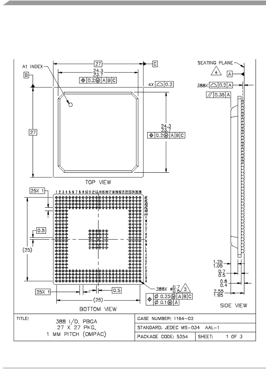

MCF548x Reference Manual, Rev. 3
Freescale Semiconductor A-1
Appendix A
MCF548x Memory Map
Table A-1 lists an overview of the memory map for the on-chip modules.
Table A-1. MCF548x Module Memory Map Overview
Address Name
(abbreviation) Description
MBAR + 0x0000 –
0x00FF SIU SIU overview registers
MBAR + 0x0100 –
0x01FF SDRAMC SDRAM Controller registers
MBAR + 0x0200 –
0x02FF XARB XLB Arbiter registers
MBAR + 0x0300 –
0x04FF Reserved —
MBAR + 0x0500 –
0x05FF FBIC FlexBus Interface Controller registers
MBAR + 0x0600 –
0x06FF Reserved —
MBAR + 0x0700 –
0x07FF INTC Interrupt Controller registers
MBAR + 0x0800 –
0x08FF GPT General Purpose Timer registers
MBAR + 0x0900 –
0x09FF SLT Slice Timer registers
MBAR + 0x0A00 –
0x0AFF GPIO GPIO registers and Pin configuration (from reindeer
project)
MBAR + 0x0B00 –
0x0BFF PCI PCI registers
MBAR + 0x0C00 –
0x0CFF PCI ARB PCI Arbiter registers
MBAR + 0x0D00 –
0x0DFF EXTDMA External DMA request registers
MBAR + 0x0E00 –
0x0EFF Reserved —
MBAR + 0x0F00 –
0x0FFF EPORT Edge Port registers
MBAR + 0x1000 –
0x7EFF Reserved —
MBAR + 0x7F00 –
0x7FFF CTM Comm Timer registers

MCF548x Reference Manual, Rev. 3
A-2 Freescale Semiconductor
MBAR + 0x8000 –
0x80FF DMA Multi-Channel DMA registers
MBAR + 0x8100 –
0x83FF Reserved —
MBAR + 0x8400 –
0x84FF SCPCI Multi-Channel DMA PCI registers
MBAR + 0x8500 –
0x85FF Reserved —
MBAR + 0x8600 –
0x86FF PSC0 Programmable Serial Controller registers
MBAR + 0x8700 –
0x87FF PSC1 Programmable Serial Controller registers
MBAR + 0x8800 –
0x88FF PSC2 Programmable Serial Controller registers
MBAR + 0x8900 –
0x89FF PSC3 Programmable Serial Controller registers
MBAR + 0x8A00 –
0x8AFF DSPI DMA Serial Peripheral Interface registers
MBAR + 0x8B00 –
0x8EFF Reserved —
MBAR + 0x8F00 –
0x8FFF I2C I2C registers
MBAR + 0x9000 –
0x97FF FEC0 Fast Ethernet Controller 0 registers
MBAR + 0x9800 –
0x9FFF FEC1 Fast Ethernet Controller 1 registers
MBAR + 0xA000 –
0xA7FF FLEXCAN0 FlexCAN controller
MBAR + 0xA800 –
0xAFFF FLEXCAN1 FlexCAN controller
MBAR + 0xB000 –
0xB7FF USB 2.0 USB 2.0 Device Contoller registers
MBAR + 0xB800 –
0xFFFF Reserved —
MBAR + 0x1_0000 –
0x1_7FFF SRAM 32KB System SRAM memory locations
MBAR + 0x1_8000 –
0x1_FEFF Reserved —
Table A-1. MCF548x Module Memory Map Overview (continued)
Address Name
(abbreviation) Description

MCF548x Reference Manual, Rev. 3
Freescale Semiconductor A-3
NOTE
Read and write accesses to reserved MBAR spaces will result in undefined
behavior that may result in a non-terminated bus cycle. This applies to the
reserved locations between modules and the reserved locations within valid
module address ranges.
MBAR + 0x1_FF00 –
0x1_FFFF SRAMCFG 32KB System SRAM Configuration registers.
MBAR + 0x2_0000 –
0x3_FFFF SEC Integrated Security Engine
Table A-1. MCF548x Module Memory Map Overview (continued)
Address Name
(abbreviation) Description

MCF548x Reference Manual, Rev. 3
A-4 Freescale Semiconductor

Index
MCF548x Reference Manual, Rev. 3
Freescale Semiconductor Index-1
A
Acknowledge error (ACKERR) 21-16
Addressing modes 3-18
Associated functions 15-3
B
BDM, see debug
Bit error (BITERR) 21-16
Bus off interrupt (BOFFINT) 21-17
Bus, see FlexBus 17-1
Byte lanes 17-2
C
Cache
cache-inhibited accesses 7-13
initialization 7-30
interaction with SRAM 7-1
line states 7-8
management 7-23
modes 7-12
copyback 7-13
write-through 7-12
protocol
read hit 7-15
read miss 7-14
write hit 7-15
write miss 7-14
registers
access control (ACRn) 3-13, 5-5, 5-6, 7-22
configuration (CACR) 3-13
control (CACR) 5-5, 7-19
state transitions 7-26
Collision handling 30-53
Commands
BDM 8-33–8-50
SDRAM controller 18-10–18-13
Core
branch acceleration 3-4
enhancements 3-1
pipelines 3-2
instruction fetch 3-3
operand execution 3-4
registers
address (An)3-9
condition code (CCR) 3-9
data (Dn)3-9
module base address (MBAR) 3-13
RAM base address (RAMBAR) 3-13
status (SR) 3-12
user stack pointer (A7) 3-9
vector base (VBR) 3-12, 3-37
Crypto-channel 22-3, 22-11, 22-18
D
Debug
BDM
commands
DUMP 8-39
extension words 8-33
FILL 8-41
FORCE_TA 8-44
format 8-33
GO 8-42
NOP 8-43
RAREG/RDREG 8-35
RCREG 8-45
RDMREG 8-49
READ 8-36
summary 8-32
WAREG/WDREG 8-35
WCREG 8-48
WDMREG 8-50
WRITE 8-38
receive packet 8-30
serial interface 8-30
transmit packet 8-31
breakpoint operation theory 8-51
data breakpoint/mask registers 8-22
emulator mode 8-53
enhancements 3-6
instructions 8-54, 8-60
memory map 8-10
processor halted 8-8
processor stopped 8-7
real-time trace support 8-5–8-8
registers
address attribute (BAAR) 8-15
address breakpoint (ABLR, ABHR) 8-21
attribute trigger (AATR, AATR1) 8-16

MCF548x Reference Manual, Rev. 3
Index-2 Freescale Semiconductor
configuration/status (CSR) 8-11
data breakpoint/mask (DBR, DBMR) 8-22
extended trigger definition (XTDR) 8-25
PC breakpoint ASID (PBASID) 8-24
PC breakpoint ASID control (PBAC) 8-14
program counter breakpoint/mask (PBRn,
PBMR) 8-20
trigger definition (TDR) 8-17
signals 8-2
taken branch 8-6
virtual environment 5-7
DMA
initiators 24-23
LURC 24-31
master DMA engine 24-27
memory map 24-3
prioritization 24-24
registers
current pointer (CP) 24-7
end pointer (EP) 24-8
external request address mask (EREQMASK) 24-21
external request base address (EREQBAR) 24-20
initiator mux control (IMCR) 24-13
initiator priority (IPRIORn)24-12
interrupt mask (DIMR) 24-10
interrupt pending (DIPR) 24-10
PTD control (PTD) 24-9
task base address (TaskBAR) 24-6
task control (TCRn) 24-11
task size (TSKSZn)24-14
variable pointer (VP) 24-8
signals
DACKn24-3
DREQn24-3
task initialization 24-23
task instantiation 24-28
task table 24-3
termination of loop 24-27
variable table 24-4
DSPI
baud rate 27-23, 27-33
block diagram 27-2
changing queues 27-33
clock delay 27-23–27-24, 27-34
DMA requests 27-31
FIFO
disabling 27-21
Rx
buffering 27-22
draining 27-22
filling 27-22
Tx
buffering 27-21
draining 27-21
filling 27-21
interrupts 27-31–27-32
memory map 27-4
registers
clock and transfer attributes 0–7 (DCTARn)27-7
DMA/interrupt request select (DIRSR) 27-13
module configuration (DMCR) 27-5
Rx FIFO (DRFR) 27-16
Rx FIFO debug 0–3 (DRFDRn) 27-17
status (DSR) 27-11
transfer count (DTCR) 27-7
Tx FIFO (DTFR) 27-15
Tx FIFO debug 0–3 (DTFDRn) 27-17
signals
peripheral chip select 5/peripheral chip select strobe
(DSPICS5/PCSS) 27-3
peripheral chip select/slave select
(DSPICS0/SS) 27-3
peripheral chip selects 2–3 (DSPICSn)27-3
serial clock (DSPISCK) 27-4
serial input (DSPISIN) 27-4
serial output (DSPISOUT) 27-4
start and stop 27-19
transfer formats 27-25–27-30
E
EMAC
data representation 3-17, 4-12
hardware support 3-4
instructions
execution timing 4-11
summary 4-11
MAC, comparison 4-1
memory map 4-5
opcodes 4-13
operation
general 4-2
rounding 4-8
saving and restoring 4-9
registers
mask (MASK) 4-10
status (MACSR) 4-5
EPORT
memory map 14-2
registers
data direction (EPDDR) 14-3
flag (EPFR) 14-5
pin assignment (EPPAR) 14-3
pin data (EPPDR) 14-5
port data (EPDR) 14-4

MCF548x Reference Manual, Rev. 3
Freescale Semiconductor Index-3
port interrupt enable (EPIER) 14-4
Error counters 21-30
Ethernet
address recognition 30-48
collision handling 30-53
errors
handling 30-54
reception
CRC 30-55
frame length 30-55
non-octet 30-55
overrun 30-55
truncation 30-55
transmission
attempts limit expired 30-54
heartbeat 30-54
late collision 30-54
underrun 30-54
frame reception 30-47
frame transmission 30-46
hash table 30-49
initialization 30-43
interpacket gap time 30-53
memory map
control and stauts registers 30-7
MIB block counters 30-8
operation
10/100 Mbps MII 30-3, 30-46
7-wire serial 30-4, 30-46
full duplex 30-3, 30-52
half duplex 30-3
loopback 30-53
registers
control (ECR) 30-13
descriptor group lower address (GALR) 30-24
descriptor individual lower (IALR) 30-23
descriptor individual upper (IAUR) 30-22
FEC transmit FIFO watermark (FECTFWR) 30-25
interrupt event (EIR) 30-10
interrupt mask (EIMR) 30-12
MIB control (MIBC) 30-17
MII management frame (MMFR) 30-14
MII speed control (MSCR) 30-15
opcode/pause duration (OPD) 30-22
physical address low (PALR) 30-20
receive control (RCR) 30-17
transmit control (TCR) 30-19
Exceptions
FPU 6-17–6-23
overview 3-36
precise faults 3-42
processor 3-39
stack frame definition 3-38
F
FEC, see Ethernet
FlexBus
address latch 17-2
burst cycles 17-26–??
byte lanes 17-2
chip select operation 17-6
connections 17-12
data alignment 17-12
data transfer 17-12
cycle states 17-14
read cycle 17-15
write cycle 17-16
errors 17-32
misaligned operands 17-31
registers
chip select address (CSARn) 17-8
chip select control (CSCRn) 17-10
chip select mask (CSMRn)17-9
signals
address/data (ADn)17-4
byte selects (BE/BWEn)17-5
chip select (FBCSn) 17-4
output enable (OE)17-5
read/write (R/W) 17-4
transfer acknowledge (TA) 17-5
transfer burst (TBST) 17-4
transfer size (TSIZn) 17-4
transfer start (TS) 17-4
FlexCAN
bit timing 21-28
error counters 21-30
initialization 21-31
interrupts 21-31
memory map 21-5
message buffers
frames
overload 21-28
remote 21-27
self-received 21-25
handling 21-25
locking and releasing 21-27
receive deactivation 21-26
serial message buffers 21-26
transmit deactivation 21-26
receive
codes 21-21
error status flag (RXWARN) 21-17
serial 21-24
status 21-17

MCF548x Reference Manual, Rev. 3
Index-4 Freescale Semiconductor
structure 21-19
time stamp 21-28
transmit
codes 21-22
error status flag (TXWARN) 21-16
priority 21-24
operation 21-19–21-31
bit timing configuration 21-29
debug mode 21-3
listen-only mode 21-4
receive process 21-24
registers
control (CANCTRL) 21-8
error and status (ESTAT) 21-15
interrupt flag (IFLAG) 21-18
interrupt mask (IMASK) 21-17
module configuration (CANMCR) 21-6
Rx 14 mask (RX14MASK) 21-13
Rx 15 Mask (RX15MASK) 21-13
Rx global mask (RXGMASK) 21-12
transmit process 21-23
FPU
data formats 3-17
floating-point 6-3
signed-integer 6-3
data types
denormalized numbers 6-5
infinities 6-4
normalized numbers 6-4
not-a-number 6-5
zeros 6-4
exceptions 6-17–6-23
BSUN 6-19
DZ 6-22
IDE 6-20
INAN 6-20
INEX 6-23
OPERR 6-21
OVFL 6-21
UNFL 6-22
instructions
execution timing 6-27
general 6-25
MC68000, differences 6-28
post-processing 6-14
conditional testing 6-15
overflow 6-14
round 6-14
underflow 6-14
registers
control (FPCR) 6-7
data (FPn)6-7
instruction address (FPIAR) 6-10
status (FPSR) 6-9
results
intermediate 6-11
rounding 6-12
state frames 6-23
Frame reception, FlexCAN 21-24
Frame transmission, FlexCAN 21-23
G
GPIO
registers
DMA pin assignment (PAR_DMA) 15-23
DSPI pin assignment (PAR_DSPI) 15-30
FEC/I2C/IRQ pin assignment
(PAR_FECI2CIRQ) 15-23
FlexBus chip select pin assignment
(PAR_FBCS) 15-22
general purpose timer pin assignment
(PAR_TIMER) 15-31
PCI grant pin assignment (PAR_PCIBG) 15-25
PCI request pin assignment (PAR_PCIBR) 15-26
port clear output data (PCLRR_x) 15-18–15-20
port x data direction (PDDR_x) 15-11–15-14
port x output data (PODR_x) 15-8–15-11
port x pin assignment (PAR_x) 15-21
port x pin data/set data (PPDSDR_x) 15-14–15-17
PSC0 pin assignment (PAR_PSC0) 15-29
PSC1 pin assignment (PAR_PSC1) 15-28
PSC2 pin assignment (PAR_PSC2) 15-28
PSC3 pin assignment (PAR_PSC3) 15-27
signals 15-3–15-7
H
Hash table 30-49
I
I2C
acknowledge 28-10
block diagram 28-1
clock synchronization 28-11
data transfer 28-9
handshaking 28-12
initialization 28-12–28-18
memory map 28-3
registers
address (I2AR) 28-3
control (I2CR) 28-5
data I/O (I2DR) 28-7
frequency divider (I2FDR) 28-4
interrupt control (I2ICR) 28-7
status (I2SR) 28-5

MCF548x Reference Manual, Rev. 3
Freescale Semiconductor Index-5
repeated start 28-11
signals
SCL 28-2
SDA 28-2
START 28-9
STOP 28-9
Instructions
architecture additions 3-19
branch acceleration 3-4
debug 8-54, 8-60
EMAC
execution timing 4-11
summary 4-11
execution timing 3-27
branch 3-33
EMAC 3-34
FPU 3-35
miscellaneous 3-32
MOVE 3-28
one-operand 3-30
two-operand 3-31
fetch pipeline 3-3
JTAG
BYPASS 23-9
CLAMP 23-9
ENABLE_TEST_CTRL 23-9
EXTEST 23-8
HIGHZ 23-9
IDCODE 23-8
SAMPLE/PRELOAD 23-8
MOVEC 8-45
PULSE 8-6
STOP 8-7, 8-29
summary 3-22
WDDATA 8-6
Interrupt controller
features 13-1
interrupts
FlexCAN 21-31
prioritization 13-3
recognition 13-3
sources 13-12
vector determination 13-3
memory map 13-4
operation 13-1–13-3
registers
(IACKLPRn)13-10
interrupt control (ICRnx) 13-11
interrupt force high/low (INTFRCHn,
INTFRCLn)13-8
interrupt pending high/low (IPRHn, IPRLn)13-5
interrupt request level (IRLRn)13-10
level n IACK (LnIACK) 13-13
mask high/low (IMRHn, n) 13-7
software IACK (SWIACKR) 13-13
Interrupts
DSPI 27-31
PCI arbiter 20-10
PCI controller 19-70
processor 26-48
J
JTAG
instructions
BYPASS 23-9
CLAMP 23-9
ENABLE_TEST_CTRL 23-9
EXTEST 23-8
HIGHZ 23-9
IDCODE 23-8
SAMPLE/PRELOAD 23-8
low-power modes 23-9
memory map 23-4
operation
nonscan chain 23-9
registers
boundary scan 23-6
bypass 23-5
IDCODE 23-4
instruction shift (IR) 23-4
JTAG_CFM_CLKDIV 23-5
TEST_CTRL 23-5
signals
MTMOD0 23-2
test clock input (TCK) 23-3, 23-9
test data input/development serial input
(TDI/DSI) 23-3
test data output/development serial output
(TDO/DSO) 23-4
test mode select/breakpoint (TMS/BKPT) 23-3
test reset/development serial clock
(TRST/DSCLK) 23-4
TAP controller 23-6
L
Listen-only mode 21-4
Loop-back mode 21-4, 21-9
Low-power modes
JTAG 23-9
LURC 24-31
M
MAC, see EMAC
MBAR 3-13

MCF548x Reference Manual, Rev. 3
Index-6 Freescale Semiconductor
Mechanical data
case drawing 31-20
diagram 31-8
pinout 31-1
Memory maps
debug 8-10
DMA 24-3
DSPI 27-4
EMAC 4-5
EPORT 14-2
Ethernet
control and status registers 30-7
MIB block counters 30-8
FlexCAN 21-5
I2C 28-3
interrupt controller 13-4
JTAG 23-4
MMU 5-11
PCI controller 19-4
PSC 26-3
SEC 22-8
SIU 9-1
SRAM 16-2
timers
CTM 25-3
GPT 11-2
SLT 12-1
USB 29-4
Message buffers
frames
overload 21-28
remote 21-27
self-received 21-25
handling 21-25
receive
codes 21-21
deactivation 21-26
error status flag (RXWARN) 21-17
serial 21-24
structure 21-19
time stamp 21-28
transmit
codes 21-22
deactivation 21-26
error status flag (TXWARN) 21-16
priority 21-24
MMU
access 5-4
access error 5-5, 5-8
architecture 5-1–5-3
cache addresses 5-4
effective address 5-9
hit determination 5-6
instructions 5-23
memory map 5-11
precise faults 5-4, 5-7
registers
base address (MMUBAR) 5-5, 5-10
control (MMUCR) 5-11
fault, test, or TLB address (MMUAR) 5-15
operation (MMUOR) 5-12
read/write tag and data entry (MMUTR,
MMUDR) 5-16
status (MMUSR) 5-14
stack pointers 5-5, 5-7
supervisor protection 5-7
TLB
address fields 5-20
general 5-18
locked entries 5-22
replacement algorithm 5-21
virtual mode 5-4
P
Pause frame 30-52
PCI arbiter
arbitration
examples 20-7
hidden bus 20-6
latency 20-7
scheme 20-6
interrupts 20-10
registers
control (PACR) 20-3
PCI controller
bus
protocol 19-48–??
interrupts 19-70
memory map 19-4
registers
base address 0 (PCIBAR0) 19-11
base address 1 (PCIBAR1) 19-12
cardbus CIS pointer (PCICCPR) 19-12
configuration 1 (PCICR1) 19-10
configuration 2 (PCICR2) 19-13
configuration address (PCICAR) 19-22
device ID/vendor ID (PCIIDR) 19-7
global status/control (PCIGSCR) 19-14
initiator control (PCIICR) 19-20
initiator status (PCIISR) 19-21
initiator window 0 base/translation address
(PCIIW0BTAR) 19-17
initiator window 1 base/translation address
(PCIIW1BTAR) 19-18

MCF548x Reference Manual, Rev. 3
Freescale Semiconductor Index-7
initiator window 2 base/translation address
(PCIIW2BTAR) 19-19
initiator window configuration (PCIIWCR) 19-19
revision ID/class code (PCICCRIR) 19-9
Rx done counts (PCIRDCR) 19-41
Rx enable (PCIRER) 19-38
Rx FIFO alarm (PCIRFAR) 19-46
Rx FIFO control (PCIRFCR) 19-45
Rx FIFO data (PCIRFDR) 19-43
Rx FIFO status (PCIRFSR) 19-44
Rx FIFO write pointer (PCIRFWPR) 19-47
Rx next address (PCIRNAR) 19-40
Rx packet size (PCIRPSR) 19-36
Rx start address (PCIRSAR) 19-36
Rx status (PCIRSR) 19-42
Rx transaction control (PCIRTCR) 19-37
status/command (PCISCR) 19-7
subsystem ID/subsystem vendor ID (PCISID) 19-12
target base address translation 0 (PCITBATR0) 19-15
target base address translation 1 (PCITBATR1) 19-16
target control (PCITCR) 19-16
Tx done counts (PCITDCR) 19-28
Tx enable (PCITER) 19-26
Tx FIFO alarm (PCITFAR) 19-33
Tx FIFO control (PCITFCR) 19-32, 19-33
Tx FIFO data (PCITFDR) 19-31
Tx FIFO read pointer (PCITFRPR) 19-34
Tx FIFO status (PCITFSR) 19-31, 19-32, 19-33
Tx FIFO write pointer (PCITFWPR) 19-35
Tx last word register (PCITLWR) 19-28
Tx next address (PCITNAR) 19-27
Tx packet size (PCITPSR) 19-23
Tx start address (PCITSAR) 19-24
Tx status (PCITSR) 19-29
Tx transaction control (PCITTCR) 19-25
signals
clock (CLKIN) 19-3
frame (PCIFRAME) 19-3
parity error (PCIPERR) 19-3
stop (PCISTOP) 19-3
Program counter 3-9
PSC
baud rate calculation 26-21
block diagram 26-1
interrrupts 26-48
memory map 26-3
modes
AC97 26-39, 26-51
FIR 26-42, 26-54
clock divide ratio 26-27
MIR 26-41, 26-53
modem16 26-38, 26-51
modem8 26-37, 26-50
multidrop 26-36
SIR 26-41, 26-52
UART 26-35, 26-49
automatic echo 26-46
local loopback 26-46
remote loopback 26-47
registers
auxiliary control (PSCACRn) 26-18
clock select (PSCCSRn)26-10
command (PSCCRn) 26-11
counter timer (PSCCTURn, PSCCTLRn)26-21
infrared control 1 (PSCIRCR1n)26-24
infrared control 2 (PSCIRCR2n)26-24
infrared FIR divide (PSCIRFDRn)26-26
infrared MIR divide (PSCIRMDRn) 26-25
infrared SIR divide (PSCIRSDRn)26-25
input port (PSCIP) 26-21
input port (PSCIPn)26-21
input port change (PSCIPCRn) 26-17
interrupt mask (PSCIMRn) 26-19
interrupt status (PSCISRn) 26-18
mode 1 (PSCMR1) 26-5
mode 1 (PSCMR1n)26-5
mode 2 (PSCMR2n)26-6
output port bit reset (PSCOPRESETn)26-22
output port bit set (PSCOPSETn) 26-22
PSC/IrDA control (PSCSICRn) 26-23
receiver and transmitter buffer (PSCRBn,
PSCTBn)26-14
RxFIFO and TxFIFO alarm (PSCRFARn,
PSCTFARn) 26-32
RxFIFO and TxFIFO control (PSCRFCRn,
PSCTFCRn)26-30
RxFIFO and TxFIFO counter (PSCRFCRn,
PSCTFCRn)26-27
RxFIFO and TxFIFO data (PSCRFDRn,
PSCTFDRn) 26-27
RxFIFO and TxFIFO last read frame pointer
(PSCRLRFPn, PSCTLRFPn)26-33
RxFIFO and TxFIFO last write frame pointer
(PSCRLWFPn, PSCTLWFPn) 26-34
RxFIFO and TxFIFO read pointer (PSCRFRPn,
PSCTFRPn) 26-32
RxFIFO and TxFIFO status (PSCRFSRn,
PSCTFSRn) 26-28
RxFIFO and TxFIFO write pointer (PSCRFWPn,
PSCTFWPn) 26-33
status (PSCSRn) 26-8
reset 26-47

MCF548x Reference Manual, Rev. 3
Index-8 Freescale Semiconductor
R
RAMBAR 3-13
Registers
cache
access control (ACRn) 3-13, 5-5, 5-6, 7-22
configuration (CACR) 3-13
control (CACR) 5-5, 7-19
core
address (An)3-9
condition code (CCR) 3-9
data (Dn)3-9
module base address (MBAR) 3-13
RAM base address (RAMBAR) 3-13
status (SR) 3-12
user stack pointer (A7) 3-9
vector base (VBR) 3-12, 3-37
debug
address attribute (BAAR) 8-15
address breakpoint (ABLR, ABHR) 8-21
attribute trigger (AATR, AATR1) 8-16
configuration/status (CSR) 8-11
data breakpoint/mask (DBR, DBMR) 8-22
extended trigger definition (XTDR) 8-25
PC breakpoint AISD (PBASID) 8-24
PC breakpoint ASID control (PBAC) 8-14
program counter breakpoint/mask (PBRn,
PBMR) 8-20
trigger definition (TDR) 8-17
DMA
current pointer (CP) 24-7
end pointer (EP) 24-8
external request address mask (EREQMASK) 24-21
external request base address (EREQBAR) 24-20
initiator mux control (IMCR) 24-13
initiator priority (IPRIORn)24-12
interrupt mask (DIMR) 24-10
interrupt pending (DIPR) 24-10
PTD control (PTD) 24-9
task base address (TaskBAR) 24-6
task control (TCRn) 24-11
task size (TSKSZn24-14
variable pointer (VP) 24-8
DSPI
clock and transfer attributes 0–7 (DCTARn) 27-7
DMA/interrupt request select (DIRSR) 27-13
module configuration (DMCR) 27-5
Rx FIFO (DRFR) 27-16
Rx FIFO debug 0–3 (DRFDRn) 27-17
status (DSR) 27-11
transfer count (DTCR) 27-7
Tx FIFO (DTFR) 27-15
Tx FIFO debug 0–3 (DTFDRn)27-17
EMAC
mask (MASK) 4-10
status (MACSR) 4-5
EPORT
data direction (EPDDR) 14-3
flag (EPFR) 14-5
pin assignment (EPPAR) 14-3
pin data (EPPDR) 14-5
port data (EPDR) 14-4
port interrupt enable (EPIER) 14-4
Ethernet
control (ECR) 30-13
descriptor group lower address (GALR) 30-24
descriptor individual lower (IALR) 30-23
descriptor individual upper address (IAUR) 30-22
FEC transmit FIFO watermark (FECTFWR) 30-25
interrupt event (EIR) 30-10
interrupt mask (EIMR) 30-12
MIB control (MIBC) 30-17
MII management frame (MMFR) 30-14
MII speed control (MSCR) 30-15
opcode/pause duration (OPD) 30-22
physical address low (PALR) 30-20
receive control (RCR) 30-17
transmit control (TCR) 30-19
FlexBus
chip select address (CSARn) 17-8
chip select control (CSCRn) 17-10
chip select mask (CSMRn)17-9
FlexCAN
control (CANCTRL) 21-8
error and status (ESTAT) 21-15
interrupt flag (IFLAG) 21-18
interrupt mask (IMASK) 21-17
module configuration (CANMCR) 21-6
Rx 14 mask (RX14MASK) 21-13
Rx 15 Mask (RX15MASK) 21-13
Rx global mask (RXGMASK) 21-12
FPU
control (FPCR) 6-7
data (FPn)6-7
instruction address (FPIAR) 6-10
status (FPSR) 6-9
GPIO
DMA pin assignment (PAR_DMA) 15-23
DSPI pin assignment (PAR_DSPI) 15-30
FEC/I2C/IRQ pin assignment
(PAR_FECI2CIRQ) 15-23
FlexBus chip select pin assignment
(PAR_FBCS) 15-22
general purpose timer pin assignment
(PAR_TIMER) 15-31

MCF548x Reference Manual, Rev. 3
Freescale Semiconductor Index-9
PCI grant pin assignment (PAR_PCIBG) 15-25
PCI request pin assignment (PAR_PCIBR) 15-26
port clear output data (PCLRR_x) 15-18–15-20
port x data direction (PDDR_x) 15-11–15-14
port x output data (PODR_x) 15-8–15-11
port x pin assignment (PAR_x)15-21
port x pin data/set data (PPDSDR_x) 15-14–15-17
PSC0 pin assignment (PAR_PSC0) 15-29
PSC1 pin assignment (PAR_PSC1) 15-28
PSC2 pin assignment (PAR_PSC2) 15-28
PSC3 pin assignment (PAR_PSC3) 15-27
I2C
address (I2AR) 28-3
control (I2CR) 28-5
data I/O (I2DR) 28-7
frequency divider (I2FDR) 28-4
interrupt control (I2ICR) 28-7
status (I2SR) 28-5
interrupt controller
interrupt acknowledge level and priority
(IACKLPRn)13-10
interrupt control (ICRnx) 13-11
interrupt force high/low (INTFRCHn,
INTFRCLn)13-8
interrupt pending high/low (IPRHn, IPRLn)13-5
interrupt request level (IRLRn)13-10
level n IACK (LnIACK) 13-13
mask high/low (IMRHn, n) 13-7
software IACK (SWIACKR) 13-13
JTAG
boundary scan 23-6
bypass 23-5
IDCODE 23-4
instruction shift (IR) 23-4
JTAG_CFM_CLKDIV 23-5
TEST_CTRL 23-5
MMU
base address (MMUBAR) 5-5, 5-10
control (MMUCR) 5-11
fault, test, or TLB address (MMUAR) 5-15
operation (MMUOR) 5-12
read/write tag and data entry (MMUTR,
MMUDR) 5-16
status (MMUSR) 5-14
PCI arbiter
control (PACR) 20-3
PCI controller
base address 0 (PCIBAR0) 19-11
base address 1 (PCIBAR1) 19-12
cardbus CIS pointer (PCICCPR) 19-12
configuration 1 (PCICR1) 19-10
configuration 2 (PCICR2) 19-13
configuration address (PCICAR) 19-22
device ID/vendor ID (PCIIDR) 19-7
global status/control (PCIGSCR) 19-14
initiator control (PCIICR) 19-20
initiator status (PCIISR) 19-21
initiator window 0 base/translation address
(PCIIW0BTAR) 19-17
initiator window 1 base/translation address
(PCIIW1BTAR) 19-18
initiator window 2 base/translation address
(PCIIW2BTAR) 19-19
initiator window configuration (PCIIWCR) 19-19
revision ID/class code (PCICCRIR) 19-9
Rx done counts (PCIRDCR) 19-41
Rx enable (PCIRER) 19-38
Rx FIFO (PCIRFDR) 19-43
Rx FIFO alarm (PCIRFAR) 19-46
Rx FIFO control (PCIRFCR) 19-45
Rx FIFO status (PCIRFSR) 19-44
Rx FIFO write pointer (PCIRFWPR) 19-47
Rx next address (PCIRNAR) 19-40
Rx packet size (PCIRPSR) 19-36
Rx start address (PCIRSAR) 19-36
Rx status (PCIRSR) 19-42
Rx transaction control (PCIRTCR) 19-37
status/command (PCISCR) 19-7
subsystem ID/subsystem vendor ID (PCISID) 19-12
target base address translation 0 (PCITBATR0) 19-15
target base address translation 1 (PCITBATR1) 19-16
target control (PCITCR) 19-16
Tx done counts (PCITDCR) 19-28
Tx enable (PCITER) 19-26
Tx FIFO alarm (PCITFAR) 19-33
Tx FIFO control (PCITFCR) 19-32, 19-33
Tx FIFO data (PCITFDR) 19-31
Tx FIFO read pointer (PCITFRPR) 19-34
Tx FIFO status (PCITFSR) 19-31, 19-32, 19-33
Tx FIFO write pointer (PCITFWPR) 19-35
Tx last word register (PCITLWR) 19-28
Tx next address (PCITNAR) 19-27
Tx packet size (PCITPSR) 19-23
Tx start address (PCITSAR) 19-24
Tx status (PCITSR) 19-29
Tx transaction control (PCITTCR) 19-25
programming model table 3-13
PSC
auxiliary control (PSCACRn) 26-18
clock select (PSCCSRn)26-10
command (PSCCRn) 26-11
counter timer (PSCCTURn, PSCCTLRn)26-21
infrared control 1 (PSCIRCR1n)26-24
infrared control 2 (PSCIRCR2n)26-24

MCF548x Reference Manual, Rev. 3
Index-10 Freescale Semiconductor
infrared FIR divide (PSCIRFDRn)26-26
infrared MIR divide (PSCIRMDRn)26-25
infrared SIR divide (PSCIRSDRn)26-25
input port (PSCIP) 26-21
input port (PSCIPn) 26-21
input port change (PSCIPCRn) 26-17
interrupt mask (PSCIMRn)26-19
interrupt status (PSCISRn)26-18
mode 1 (PSCMR1) 26-5
mode 1 (PSCMR1n) 26-5
mode 2 (PSCMR2n) 26-6
output port bit reset (PSCOPRESETn) 26-22
output port bit set (PSCOPSETn) 26-22
PSC/IrDA control (PSCSICRn)26-23
receiver and transmitter buffer (PSCRBn,
PSCTBn)26-14
RxFIFO and TxFIFO alarm (PSCRFARn,
PSCTFARn) 26-32
RxFIFO and TxFIFO control (PSCRFCRn,
PSCTFCRn) 26-30
RxFIFO and TxFIFO counter (PSCRFCRn,
PSCTFCRn) 26-27
RxFIFO and TxFIFO data (PSCRFDRn,
PSCTFDRn)26-27
RxFIFO and TxFIFO last read frame pointer
(PSCRLRFPn, PSCTLRFPn) 26-33
RxFIFO and TxFIFO last write frame pointer
(PSCRLWFPn, PSCTLWFPn)26-34
RxFIFO and TxFIFO read pointer (PSCRFRPn,
PSCTFRPn)26-32
RxFIFO and TxFIFO status (PSCRFSRn,
PSCTFSRn)26-28
RxFIFO and TxFIFO write pointer (PSCRFWPn,
PSCTFWPn) 26-33
status (PSCSRn) 26-8
SDRAM controller
chip select configuration (CSnCFG) 18-18
configuration 1 (SDCFG1) 18-21
configuration 2 (SDCFG2) 18-23
control (SDCR) 18-20
drive strength (SDRAMDS) 18-17
mode/extended mode (SDMR) 18-19
SEC
AESU interrupt mask (AESIMR) 22-54
AESU interrupt status (AESISR) 22-53
AESU reset control (AESRCR) 22-50
AESU status (AESSR) 22-51
AFEU interrupt mask (AFIMR) 22-32
AFEU interrupt status (AFISR) 22-31
AFEU reset control (AFRCR) 22-28
AFEU status (AFSR) 22-29
crypto-channel configuration (CCCRn) 22-19
crypto-channel current descriptor pointer
(CDPRn) 22-27
crypto-channel pointer status (CCPSRn) 22-21
data packet descriptor buffer (CDBUFn) 22-28
DEU interrupt mask (DIMR) 22-39
DEU interrupt status (DISR) 22-37
DEU reset control (DRCR) 22-34
DEU status (DSR) 22-35
EU assignment control (EUACR) 22-11
EU assignment status (EUASR) 22-13
fetch (FRn) 22-27
ID (SIDR) 22-16
interrupt control (SICR) 22-14
interrupt mask (SIMR) 22-14
interrupt status (SISR) 22-14
master control (SMCR) 22-17
master error address (MEAR) 22-18
MDEU interrupt mask (MDIMR) 22-44
MDEU interrupt status (MDISR) 22-43
MDEU reset control (MDRCR) 22-41
MDEU status (MDSR) 22-41
RNG interrupt mask (RNGIMR) 22-49
RNG interrupt status (RNGISR) 22-48
RNG reset control (RNGRCR) 22-46
RNG status (RNGSR) 22-47
SIU
JTAG device ID (JTAGID) 9-5
module base address (MBAR) 9-2
reset status (RSR) 9-5
SEC sequential access control (SECSACR) 9-4
system breakpoint control (SBCR) 9-3
SRAM
base address (RAMBAR0, RAMBAR1) 7-2
configuration (SSCR) 16-3
TCC, DMA read channel (TCCRDR) 16-5
TCC, DMA write channel (TCCRDW) 16-6
TCC, SEC (TCCRSEC) 16-7
transfer count configuration (TCCR) 16-4
timers
CTM
configuration, fixed timer (CTCRn) 25-4
configuration, variable timer (CTCRn) 25-5
GPT
counter input (GCIRn) 11-5
enable and mode select (GMSn) 11-3
PWM configuration (GPWMn)11-6
status (GSRn) 11-7
SLT
control (SCRn) 12-2
status (SSRn) 12-4
terminal count (STCNTn) 12-2
timer count (SCNTn)12-3

MCF548x Reference Manual, Rev. 3
Freescale Semiconductor Index-11
USB
application interface update (IFUR) 29-22
application interrupt mask (USBAIMR) 29-17
application interrupt status (USBIASR) 29-16
bitstuffing error counter (BSECNT) 29-24
bmrequest type (BMRTR) 29-31
brequest type (BRTR) 29-32
configuration attribute (CFGAR) 29-19
configuration interface (IFRn)29-22
configuration value (CFGR) 29-19
control (USBCR) 29-10
counter overflow (CNTOVR) 29-26
CRC error counter (CRCECNT) 29-24
descriptor RAM control (DRAMCR) 29-12
descriptor RAM data (DRAMDR) 29-13
device speed (SPEEDR) 29-20
dropped packet counter (DPCNT) 29-24
endoint n sync frame 29-33
endpoint info (EPINFO) 29-18
endpoint n attribute control 29-27
endpoint n FIFO alarm (EPnFAR) 29-44
endpoint n FIFO control (EPnFCR) 29-42
endpoint n FIFO data (EPnFDR) 29-39
endpoint n FIFO RAM configuration
(EPnFRCFGR) 29-38
endpoint n FIFO read pointer (EPnFRP) 29-45
endpoint n FIFO status (EPnFSR) 29-40
endpoint n FIFO write pointer (EPnFWP) 29-45
endpoint n interface number 29-29
endpoint n interrupt mask (EPnIMR) 29-37
endpoint n interrupt status (EPnISR) 29-35
endpoint n last read frame pointer (EPnLRFP) 29-46
endpoint n last write frame pointer (EPnLWFP) 29-47
endpoint n max packet size 29-28
endpoint n status 29-30
endpoint n status and control (EPnSTAT) 29-34
endpoint transaction number (EPTNR) 29-21
error counter (PIDECNT) 29-25
frame number (FRMNUMR) 29-21
framing error counter (FRMECNT) 29-25
interrupt mask (USBIMR) 29-15
interrupt status (USBISR) 29-14
packet passed count (PPCNT) 29-23
status (USBSR) 29-9
transmitted packet counter (TXPCNT) 29-26
windex (WINDEXR) 29-33
wlength (WLENGTHR) 29-33
wvalue (WVALUER) 29-32
S
Sample Point 21-29
S-clock 21-28
SDRAM controller
block diagram 18-2
commands
ACTV 18-10
LMR, LEMR 18-11
PALL 18-11
PDWN 18-13
READ 18-10
REF 18-13
SREF 18-13
WRITE 18-10
configuration 18-4
connections 18-6–18-7
example 18-24–18-34
initialization 18-13, 18-34
interface configuration 18-25–18-33
page management 18-15
registers
chip select configuration (CSnCFG) 18-18
configuration 1 (SDCFG1) 18-21
configuration 2 (SDCFG2) 18-23
control (SDCR) 18-20
drive strength (SDRAMDS) 18-17
mode/extended mode (SDMR) 18-19
signals
address bus (SDADDRn) 18-2
bank address (SDBAn) 18-2
chip selects (SDCSn) 18-3
clock (SDCLKn)18-3
clock enable (SDCKE) 18-4
column address strobe (CAS) 18-3
data bus (SDDATAn) 18-2
data strobe (SDDQSn) 18-3
data strobe (SDRDQS) 18-4
inverted clock (SDCLKn) 18-3
memory supply (SDVDD) 18-4
reference voltage (VREF) 18-4
row address strobe (RAS) 18-3
write data byte mask (SDDMn) 18-3
write enable (SDWE) 18-3
transfer size 18-15
SEC
block diagram 22-2
controller 22-10
crypto-channel 22-3, 22-11, 22-18
descriptors 22-56–22-67
buffer 22-21
chaining 22-60
classes 22-64
null fields 22-61
static 22-65
structure 22-56

MCF548x Reference Manual, Rev. 3
Index-12 Freescale Semiconductor
execution units
access 22-11
AESU 22-6, 22-83
AFEU 22-5, 22-67
DEU 22-4, 22-72
MDEU 22-6, 22-77
multifunction data packet descriptors 22-90
multiple assignment 22-11
RNG 22-8, 22-82
memory map 22-8
registers
AESU interrupt mask (AESIMR) 22-54
AESU interrupt status (AESISR) 22-53
AESU reset control (AESRCR) 22-50
AESU status (AESSR) 22-51
AFEU interrupt mask (AFIMR) 22-32
AFEU interrupt status (AFISR) 22-31
AFEU reset control (AFRCR) 22-28
AFEU status (AFSR) 22-29
crypto-channel configuration (CCCRn) 22-19
crypto-channel current descriptor pointer
(CDPRn) 22-27
crypto-channel pointer status (CCPSRn)22-21
data packet descriptor buffer (CDBUFn) 22-28
DEU interrupt mask (DIMR) 22-39
DEU interrupt status (DISR) 22-37
DEU reset control (DRCR) 22-34
DEU status (DSR) 22-35
EU assignment control (EUACR) 22-11
EU assignment status (EUASR) 22-13
fetch (FRn) 22-27
ID (SIDR) 22-16
interrupt control (SICR) 22-14
interrupt mask (SIMR) 22-14
interrupt status (SISR) 22-14
master control (SMCR) 22-17
master error address (MEAR) 22-18
MDEU interrupt mask (MDIMR) 22-44
MDEU interrupt status (MDISR) 22-43
MDEU mode 22-78
MDEU reset control (MDRCR) 22-41
MDEU status (MDSR) 22-41
RNG interrupt mask (RNGIMR) 22-49
RNG interrupt status (RNGISR) 22-48
RNG reset control (RNGRCR) 22-46
RNG status (RNGSR) 22-47
Signals
block diagram 2-2
clock module
clock in (CLKIN) 2-22
debug
breakpoint/test mode select (BKPT/TMS) 2-30
development serial clock/test reset
(DSCLK/TRST)2-29
development serial input/test data input
(DSI/TDI) 2-30
development serial output/test data output
(DSO/TDO) 2-30
processor clock output (PSTCLK) 2-29
processor status debug data (PSTDDATAn)2-29
test clock (TCK) 2-30
DMA
DACKn24-3
DREQn24-3
DMA controller
acknowledge (DACKn)2-28
request (DREQn)2-28
DSPI
chip select (DSPICSn)2-27
peripheral chip select 5/peripheral chip select strobe
(DSPICS5/PCSS) 2-27, 27-3
peripheral chip select/slave select
(DSPICS0/SS) 27-3
peripheral chip select/slave select
(DSPICS0/SS) 2-27
peripheral chip selects 2–3 (DSPICSn)27-3
serial clock (DSPISCK) 2-27, 27-4
serial input (DSPISIN) 27-4
serial output (DSPISOUT) 27-4
synchronous serial input (DSPISIN) 2-27
synchronous serial output (DSPISOUT) 2-26
Ethernet
collision (E0COL, E1COL) 2-25
management data (E0MDIO, E1MDIO) 2-24
management data clock (E0MDC, E1MDC) 2-25
mcarrier receive sense (E0CRS, E1CRS) 2-25
receive clock (E0RXCLK, E1RXCLK) 2-25
receive data (E0RXDn, E1RXDn)2-26
receive data 0 (E0RXD0, E1RXD0) 2-25
receive data valid (E0RXDV, E1RXDV) 2-25
receive error (E0RXER, E1RXER) 2-26
transmit clock (E0TXCLK, E1TXCLK) 2-25
transmit data 0 (E0TXD0, E1TXD0) 2-25
transmit data 1–3 (E0TXDn, E1TXDn)2-25
transmit enable (E0TXEN, E1TXEN) 2-25
transmit error (E0TXER, E1TXER) 2-26
FlexBus
address/data (ADn) 2-16, 17-4
byte select (BE/BWEn)2-18
byte selects (BE/BWEn)17-5
chip select (FBCSn) 2-17, 17-4
output enable (OE) 2-18, 17-5
read/write (R/W) 2-17, 17-4
transfer acknowledge (TA) 2-18, 17-5

MCF548x Reference Manual, Rev. 3
Freescale Semiconductor Index-13
transfer burst (TBST) 2-17, 17-4
transfer size (TSIZn) 2-17, 17-4
transfer start (TS) 2-17, 17-4
FlexCAN
receive (CANRX0, CANRX1) 2-27
transmit (CANTX0, CANTX1) 2-27
general-purpose timers
inputs (TINn)2-29
outputs (TOUTn)2-29
GPIO 15-3–15-7
I2C
SCL 28-2
SDA 28-2
serial clock (SCL) 2-28
serial data (SDA) 2-28
interrupts
IRQn2-21
JTAG
MTMOD0 23-2
test clock input (TCK) 23-3, 23-9
test data input/development serial input
(TDI/DSI) 23-3
test data output/development serial output
(TDO/DSO) 23-4
test mode select/breakpoint (TMS/BKPT)23-3
test reset/development serial clock
(TRST/DSCLK) 23-4
PCI controller
addess/data (PCIADn)2-20
clock (CLKIN) 19-3
command/byte enable (PCICXBEn)2-20
device select (PCIDEVSEL)2-20
external bus grant (PCIBGn)2-21
external bus grant/request output
(PCIBG0/PCIREQOUT)2-21
external bus request (PCIBRn)2-21
external request/grant input
(PCIBR0/PCIGNTIN)2-21
frame (PCIFRAME) 19-3
frame (PCIFRM)2-20
initialization device select (PCIIDSEL) 2-20
initiator ready (PCIIRDY)2-20
parity (PCIPAR) 2-20
parity error (PCIERR) 19-3
parity error (PCIPERR)2-20
reset (PCIRESET)2-21
stop (PCISTOP) 2-21, 19-3
system error (PCISERR)2-21
target ready (PCITRDY)2-21
power and reference
EVDD 2-31
IVDD 2-31
PLLVDD 2-31
PLLVSS 2-31
SDVDD 2-31
USB_OSCAVDD 2-31
USB_OSCVDD 2-31
USB_PHYVDD 2-31
USB_PLLVDD 2-31
USBVDD 2-31
VSS 2-31
PSC
clear-to-send (PSCnCTS/PSCBCLK) 2-28
PSCnCTS/PSCBCLK 26-2
PSCnRTS/PSCFSYNC 26-2
PSCnRXD 26-2
PSCnTXD 26-3
receive serial data input (PSCnRXD) 2-28
request-to-send (PSCnRTS/PSCFSYNC) 2-28
transmit serial data output (PSCnTXD) 2-28
reset configuration
32-bit FlexBus (FBMODE) 2-23
auto acknowledge (AACONFIG) 2-24
byte enable (BECONFIG) 2-23
CLKCONFIGn2-22
FlexBus size (FBSIZE) 2-23
port size (PSCONFIG) 2-24
reset controller
reset in (RSTI)2-22
reset out (RSTO)2-22
SDRAM
clock enable 18-4
column address strobe 18-3
row address strobe 18-3
write enable 18-3
SDRAM controller
address bus (SDADDRn) 2-18, 18-2
bank address (SDBAn) 18-2
bank addresses (SDBAn)2-19
chip select (SDCSn)2-19
chip selects (SDCSn) 18-3
clock (SDCLCKn)18-3
clock (SDCLKn)2-19
clock enable (SDCKE) 2-19, 18-4
column address strobe (CAS) 2-19, 18-3
data bus (SDDATAn) 2-18, 18-2
data strobe (SDDQSn)2-19
data strobe (SDDQSn) 18-3
data strobe (SDRDQS) 18-4
inverted clock (SDCLKn) 2-19, 18-3
memory supply (SDVDD) 18-4
reference voltage (VREF) 2-20, 18-4
row address strobe (RAS) 2-19, 18-3
SDR data strobe (SDRDQS) 2-19

MCF548x Reference Manual, Rev. 3
Index-14 Freescale Semiconductor
write data byte mask (SDDMn)2-19
write data byte mask (SDDMn) 18-3
write enable (SDWE) 2-19, 18-3
test
mode (MTMODn)2-30
timers
GPT
TINn11-2
USB
differential data 29-3
differential data (USBD+, USBD–) 2-26
USBCLKIN 2-26, 29-4
USBCLKOUT 2-26, 29-4
USBRBIAS 2-26, 29-3
USBVBUS 2-26, 29-3
SIU
memory map 9-1
registers
JTAG device ID (JTAGID) 9-5
module base address (MBAR) 9-2
reset status (RSR) 9-5
SEC sequential access control (SECSACR) 9-4
system breakpoint control (SBCR) 9-3
SLT
memory map 12-1
SRAM
access 7-4
arbitration 16-8
interaction with cache 7-1
intialization 7-4
memory map 16-2
organization 16-1
power management 7-6
registers
base address (RAMBAR0, RAMBAR1) 7-2
configuration (SSCR) 16-3
TCC, DMA read channel (TCCRDR) 16-5
TCC, DMA write channel (TCCRDW) 16-6
TCC, SEC (TCCRSEC) 16-7
transfer count configuration (TCCR) 16-4
SYNC_SEG 21-29
T
TAP controller 23-6
Time stamp 21-28
Timers
CTM
block diagram 25-1
memory map 25-3
modes
baud clock generator 25-7
initiator 25-7–25-8
registers
configuration, fixed timer (CTCRn) 25-4
configuration, variable timer (CTCRn) 25-5
GPT
configuration 11-2
memory map 11-2
registers
counter input (GCIRn) 11-5
enable and mode select (GMSn) 11-3
PWM configuration (GPWMn)11-6
status (GSRn) 11-7
signals
TINn11-2
SLT
registers
control (SCRn) 12-2
status (SSRn) 12-4
terminal count (STCNTn) 12-2
timer count (SCNTn)12-3
Transmit bit error (BITERR) 21-16
Transmit Point 21-29
U
USB
corrupted frame 29-50
data transfer 29-50–29-55
exceptions 29-50
FIFO
controller 29-3
programming 29-49–29-50, 29-52
RAM manager 29-3
EPnFRCFGR 29-38
RAMSPLIT 29-11
size 29-3
initialization 29-47–29-50
memory map 29-4
packets 29-3, 29-51
registers
application interface update (IFUR) 29-22
application interrupt mask (USBAIMR) 29-17
application interrupt status (USBAISR) 29-16
bitstuffing error counter (BSECNT) 29-24
bmrequest type (BMRTR) 29-31
brequest type (BRTR) 29-32
configuration (IFRn) 29-22
configuration attribute (CFGAR) 29-19
configuration value (CFGR) 29-19
control (USBCR) 29-10
counter overflow (CNTOVR) 29-26
CRC error counter (CRCECNT) 29-24
descriptor RAM control (DRAMCR) 29-12
descriptor RAM data (DRAMDR) 29-13

MCF548x Reference Manual, Rev. 3
Freescale Semiconductor Index-15
device speed (SPEEDR) 29-20
dropped packet counter (DPCNT) 29-24
endpoint info (EPINFO) 29-18
endpoint n attribute control 29-27
endpoint n FIFO alarm (EPnFAR) 29-44
endpoint n FIFO control (EPnFCR) 29-42
endpoint n FIFO data (EPnFDR) 29-39
endpoint n FIFO RAM configuration
(EPnFRCFGR) 29-38
endpoint n FIFO read pointer (EPnFRP) 29-45
endpoint n FIFO status (EPnFSR) 29-40
endpoint n FIFO write pointer (EPnFWP) 29-45
endpoint n interface number 29-29
endpoint n interrupt mask (EPnIMR) 29-37
endpoint n interrupt status (EPnISR) 29-35
endpoint n last read frame pointer (EPnLRFP) 29-46
endpoint n last write frame pointer (EPnLWFP) 29-47
endpoint n max packet size 29-28
endpoint n status 29-30
endpoint n status and control (EPnSTAT) 29-34
endpoint n sync frame 29-33
endpoint transaction number (EPTNR) 29-21
frame register (FRMNUMR) 29-21
framing error counter (FRMECNT) 29-25
interrupt mask (USBIMR) 29-15
interrupt status (USBISR) 29-14
packet passed count (PPCNT) 29-23
PID error counter (PIDECNT) 29-25
status (USBSR) 29-9
transmitted packet counter (TXPCNT) 29-26
windex (WINDEXR) 29-33
wlength (WLENGTHR) 29-33
wvalue (WVALUER) 29-32
signals
differential data 29-3
USBCLKIN 29-4
USBCLKOUT 29-4
USBRBIAS 29-3
USBVBUS 29-3

MCF548x Reference Manual, Rev. 3
Index-16 Freescale Semiconductor

Overview
Signal Descriptions
ColdFire Core
Enhanced Multiply-Accumulate Unit (EMAC)
Memory Management Unit (MMU)
Floating-Point Unit (FPU)
Debug Support
System Integration Unit (SIU)
Local Memory
Edge Port Module (EPORT)
Index
Interrupt Controller (INTC)
20
General Purpose I/O (GPIO)
14
13
15
PCI Bus Arbiter (PCIARB)
2
3
5
6
7
8
9
4
General Purpose Timers (GPT)
Slice Timers (SLT)
Internal Clocks and Bus Architecture 10
11
12
PCI Bus Controller (PCI) 19
FlexBus
SDRAM Controller (SDRAMC)
System SRAM 16
17
18
Integrated Secuity Engine (SEC)
FlexCAN
28
IEEE 1149.1 Test Access Port (JTAG)
22
21
23
DMA Serial Peripheral Interface (DSPI)
I2C interface 27
Comm Timer Module (CTM)
Programmable Serial Controller (PSC)
Multichannel DMA (MCD) 24
26
Mechanical Data
USB 2.0 Device Controller
Fast Ethernet Controller (FEC)
1
25
29
30
31
A
IND
Register Memory Map Quick Reference

Overview
Signal Descriptions
ColdFire Core
Enhanced Multiply-Accumulate Unit (EMAC)
Memory Management Unit (MMU)
Floating-Point Unit (FPU)
Debug Support
System Integration Unit (SIU)
Local Memory
Edge Port Module (EPORT)
Index
Interrupt Controller (INTC)
20
General Purpose I/O (GPIO)
14
13
15
PCI Bus Arbiter (PCIARB)
2
3
5
6
7
8
9
4
General Purpose Timers (GPT)
Slice Timers (SLT)
Internal Clocks and Bus Architecture
10
11
12
PCI Bus Controller (PCI)
19
FlexBus
SDRAM Controller (SDRAMC)
System SRAM
16
17
18
Integrated Secuity Engine (SEC)
FlexCAN
28
IEEE 1149.1 Test Access Port (JTAG)
22
21
23
DMA Serial Peripheral Interface (DSPI)
I2C interface
27
Comm Timer Module (CTM)
Programmable Serial Controller (PSC)
Multichannel DMA (MCD)
24
26
Mechanical Data
USB 2.0 Device Controller
Fast Ethernet Controller (FEC)
1
25
29
30
31
A
IND
Register Memory Map Quick Reference
