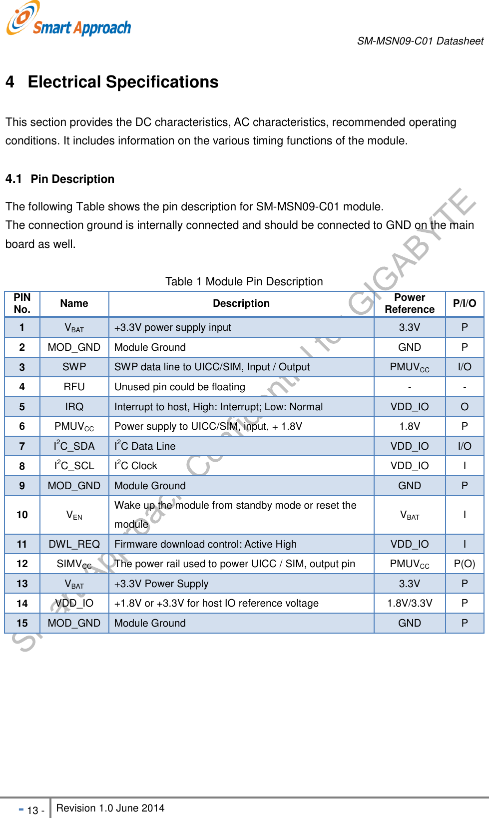
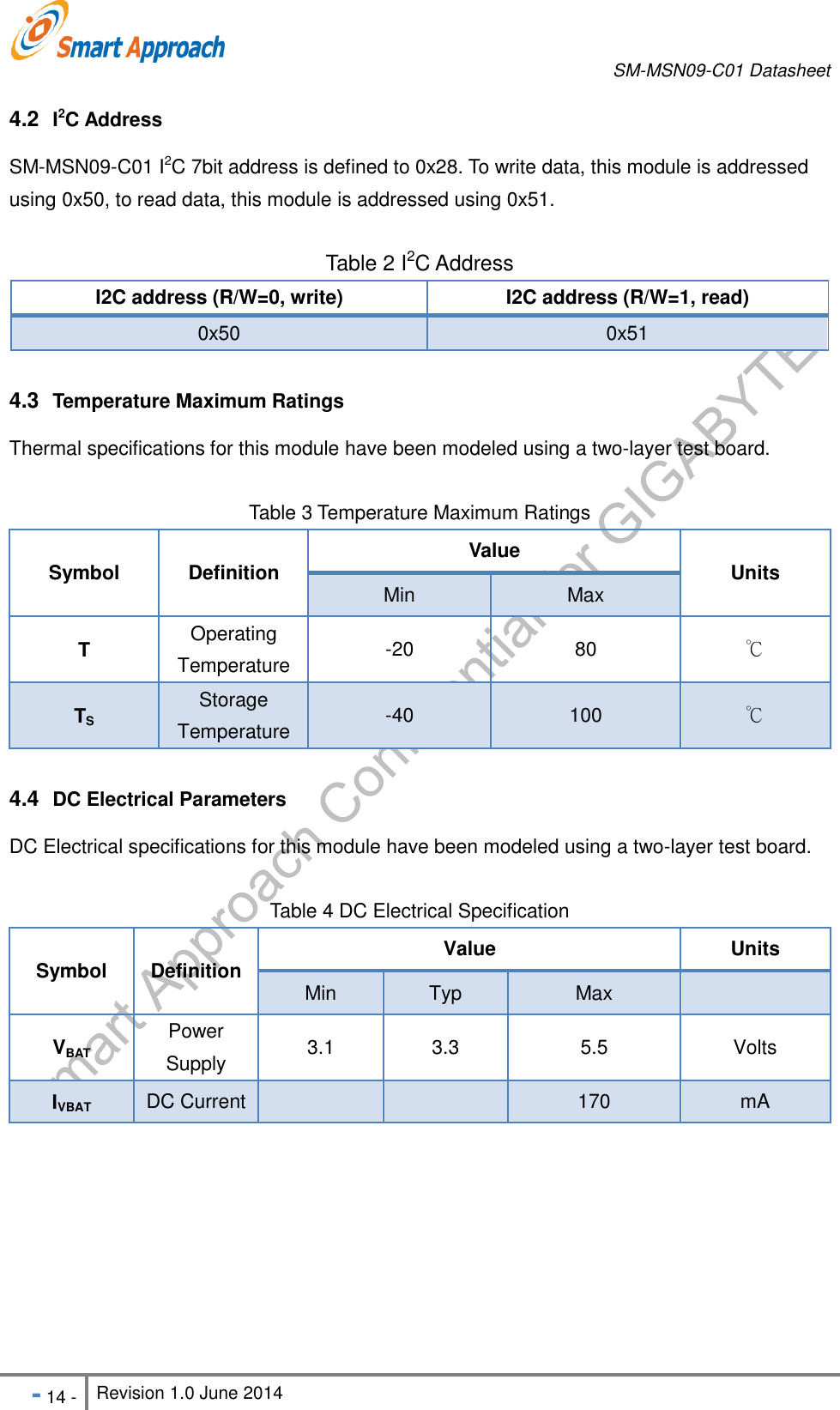
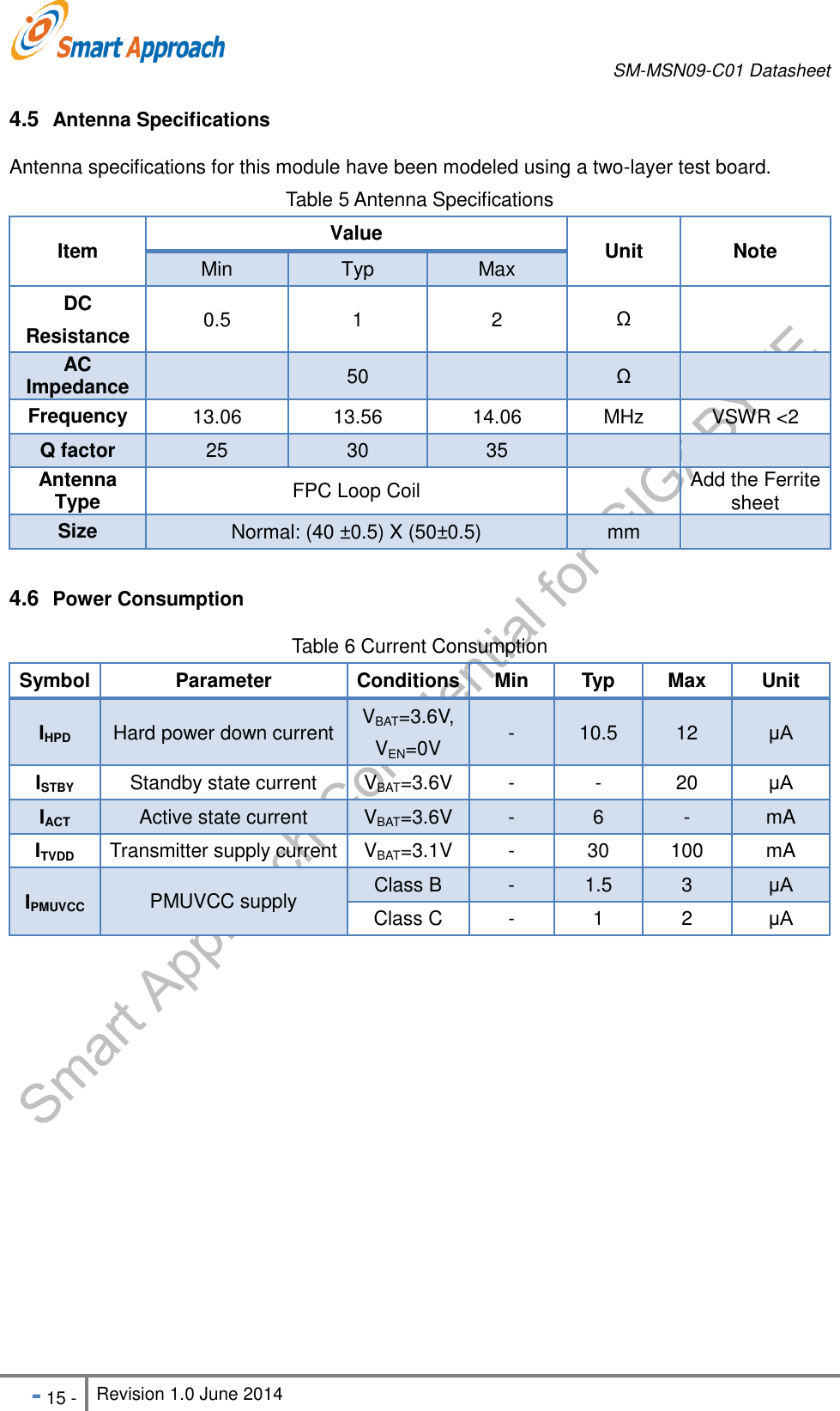
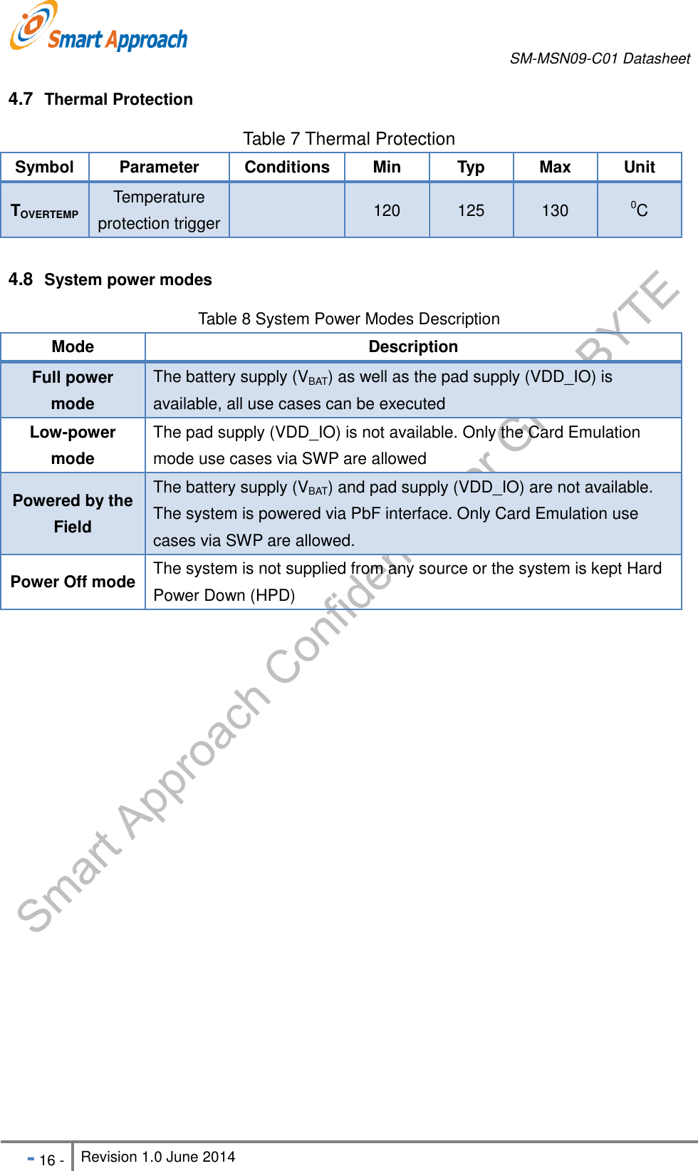
GIGA BYTE TECHNOLOGY MSN09C01 NFC Controller Module with Integrated Antenna User Manual SM MSN09 C01 UserMan

GIGA-BYTE TECHNOLOGY CO., LTD. NFC Controller Module with Integrated Antenna SM MSN09 C01 UserMan

(SM-MSN09-C01) UserMan

   Macaron N Series SM-MSN09-C01   NFC Controller Module with Integrated Antenna Datasheet Version 1.0 Smart Approach Co., Ltd. 4F,No.669,Sec.4.Chung Hsing Rd., Chutung, Hsinchu 310, Taiwan, R.O.C.  +886-3-5830303 www.smart-approach.com.tw
      SM-MSN09-C01 Datasheet   - 2 - Revision 1.0 June 2014                                                            Smart Approach Co., Ltd (“S.A.”) retains the right to make changes to its products or specifications to improve  performance,  reliability  or  manufacturability.  All  information  in  this  document,  including descriptions of features, functions, performance, technical specifications and availability, is subject to change without notice at any time. While the information furnished herein is held to be accurate and reliable, no responsibility will be assumed by Smart Approach for its use. Furthermore, the information contained herein does not convey to the purchaser of microelectronic devices any license under license under the patent right of any manufacturer. Smart Approach Co., Ltd is a registered trademark. All other products or service names used in this publication are for identification purposes only, and may be trademarks or registered trademarks of their respective companies. All other trademarks or registered trademarks mentioned herein are the property of their respective holders. Feedback on the use of any of the document is welcomed and encouraged by Smart Approach.      Please contact service@smart-approach.com.tw for your feedback or any ordering inquiry.   Please contact support@smart-approach.com.tw for any technical question.
      SM-MSN09-C01 Datasheet   - 3 - Revision 1.0 June 2014                                                            FEDERAL COMMUNICATIONS COMMISSION INTERFERENCE STATEMENT   This equipment has been tested and found to comply with the limits for a Class B digital device, pursuant to part 15 of the FCC Rules. These limits are designed to provide reasonable protection against harmful interference in a residential installation. This equipment generates, uses and can radiate radio frequency energy and, if not installed and used in accordance with the instructions, may cause harmful interference to radio communications. However, there is no guarantee that interference will not occur in a particular installation. If this equipment does cause harmful interference to radio or television reception, which can be  determined  by  turning  the  equipment  off  and  on,  the  user  is  encouraged  to  try  to  correct  the interference by one or more of the following measures:   Reorient or relocate the receiving antenna.   Increase the separation between the equipment and receiver.   Connect  the  equipment  into  an  outlet  on  a  circuit  different  from  that  to  which  the  receiver  is connected.   Consult the dealer or an experienced radio/ TV technician for help.   This device complies with part 15 of the FCC Rules. Operation is subject to the following two conditions:     This device may not cause harmful interference.   This  device  must  accept  any  interference  received,  including  interference  that  may  cause undesired operation.  CAUTION:   Any changes or modifications not expressly approved by the party responsible for compliance could void the user’s authority to operate the equipment. This device complies with Part 15 of the FCC Rules. Operation is subject to the following two conditions: (1) this device may not cause harmful interference, and   (2) this device must accept any interference received, including interference that may cause undesired operation.  Canadian Compliance Statement This  device  complies  with  Industry  Canada  license-exempt  RSS  standard(s).  Operation  is subject to the following two conditions:     This device may not cause interference, and    This  device  must  accept  any  interference,  including  interference  that  may  cause undesired operation of the device.   Cet  appareil  est  conforme  aux  norms  CNR  exemptes  de  licence  d’Industrie  Canada.  Le fonctionnement est soumis aux deux conditions suivantes:     cet appareil ne doit pas provoquer d’interférences et    cet appareil doit accepter toute interférence, y compris celles susceptibles de provoquer un fonctionnement non souhaité de l’appareil.
      SM-MSN09-C01 Datasheet   - 4 - Revision 1.0 June 2014                                                            經型式認證合格之低功率射頻電機,非經許可,公司、商號或使用者均不得擅自變更頻率、 加大功率或變更原設計之特性及功能。 低功率射頻電機之使用不得影響飛航安全及干擾合法通信;經發現有干擾現象時,應立即停用,並改善至無干擾時方得繼續使用。前項合法通信,指依電信法規定作業之無線電通信。低功率射頻電機須忍受合法通信或工業、科學及醫療用電波輻射性電機設備之干擾。  Information for the OEMs and Integrators The following statement must be included with all versions of this document supplied to an OEM or integrator, but should not be distributed to the end user. 1) This device is intended for OEM integrators only. 2) Please see the full Grant of Equipment document for other restrictions.  End Product Labeling This transmitter module is authorized only for use in device where the antenna may be installed such that 20cm may be maintained between the antenna and users. The final end product must be labeled in a visible area with the following: "Contains FCC ID: JCK-MSN09C01 ” and "Contains IC: 6655A-MSN09C01“
      SM-MSN09-C01 Datasheet   - 5 - Revision 1.0 June 2014                                                            Revision History This section describes the changes that were implemented in this document. The changes are listed by revision, starting with the most current publication. Revision 1.0   Revision 1.0 of this datasheet was published in June 2014. This was the first publication of the document.
      SM-MSN09-C01 Datasheet   - 6 - Revision 1.0 June 2014                                                            Contents REVISION HISTORY ............................................................................................................................. - 5 - CONTENTS ........................................................................................................................................... - 6 - FIGURE CONTENTS ............................................................................................................................ - 7 - TABLE CONTENTS .............................................................................................................................. - 7 - 1 INTRODUCTION .......................................................................................................................... - 8 - 2 PRODUCT OVERVIEW ................................................................................................................ - 9 - 2.1 FEATURES .............................................................................................................................. - 9 - 2.2 APPLICATION .......................................................................................................................... - 9 - 3 FUNCTIONAL DESCRIPTIONS ................................................................................................ - 11 - 3.1 COMMUNICATION OVERVIEW FOR ISO/IEC 14443A / MIFARE CONTROLLER .......................... - 12 - 4 ELECTRICAL SPECIFICATIONS .............................................................................................. - 13 - 4.1 PIN DESCRIPTION ................................................................................................................. - 13 - 4.2 I2C ADDRESS ....................................................................................................................... - 14 - 4.3 TEMPERATURE MAXIMUM RATINGS ........................................................................................ - 14 - 4.4 DC ELECTRICAL PARAMETERS .............................................................................................. - 14 - 4.5 ANTENNA SPECIFICATIONS .................................................................................................... - 15 - 4.6 POWER CONSUMPTION ......................................................................................................... - 15 - 4.7 THERMAL PROTECTION ......................................................................................................... - 16 - 4.8 SYSTEM POWER MODES ........................................................................................................ - 16 - 4.9 RESET AND DOWNLOAD CONCEPT .......................................................................................... - 17 - 4.10 NFC CONNECTION RECOMMENDATION .................................................................................. - 18 - 4.11 MAIN BOARD DESIGN REFERENCE ........................................................................................ - 18 - 5 ORDERING INFORMATION ...................................................................................................... - 19 - 6 RELIABILITY VERIFICATION .................................................................................................... - 20 - 7 NFC MODULE OUTLINE ........................................................................................................... - 21 -
      SM-MSN09-C01 Datasheet   - 7 - Revision 1.0 June 2014                                                            Figure Contents Figure 1 Typical Application ................................................................................................. - 9 - Figure 2 Typical Application II ............................................................................................ - 10 - Figure 3 Module Block Diagram ........................................................................................ - 11 - Figure 4 Transmission Modes ........................................................................................... - 12 - Figure 5 Reset via VEN pin ................................................................................................. - 17 - Figure 6 Connection Recommendation ............................................................................. - 18 - Figure 7 Main Board Design W/O UICC Reference ........................................................... - 18 - Figure 8 Antenna Module Drawing .................................................................................... - 21 - Figure 9 Module FPC Connection Footprint (Button Contact) ............................................ - 22 - Figure 10 FPC Wire Dimension ......................................................................................... - 22 - Table Contents Table 1 Module Pin Description ......................................................................................... - 13 - Table 2 I2C Address ........................................................................................................... - 14 - Table 3 Temperature Maximum Ratings ............................................................................ - 14 - Table 4 DC Electrical Specification .................................................................................... - 14 - Table 5 Antenna Specifications .......................................................................................... - 15 - Table 6 Current Consumption ............................................................................................ - 15 - Table 7 Thermal Protection ................................................................................................ - 16 - Table 8 System Power Modes Description ........................................................................ - 16 - Table 9 Power Mode Configuration .................................................................................... - 17 - Table 10 Reset Timing ....................................................................................................... - 17 - Table 11 Ordering Information Table .................................................................................. - 19 - Table 12 Reliability Item Table ........................................................................................... - 20 -
      SM-MSN09-C01 Datasheet   - 8 - Revision 1.0 June 2014                                                            1  Introduction This document consists of descriptions and specifications for both functional and physical aspects of the SM-MSN09-C01 NFC reader / writer module. In addition to the datasheet, Smart Approach maintains and extensive device-specific library of support and collateral materials that you may find useful in your application. Depending upon the Smart Approach device, this library may include:   Presentations highlighting the operational features and specifications of the device to assist in developing your own product road map.   Application notes that provide detailed descriptions of the use of the particular Smart Approach product to solve real-world problems.
      SM-MSN09-C01 Datasheet   - 9 - Revision 1.0 June 2014                                                            2  Product Overview SM-MSN09-C01 is full featured NFC controllers designed for integration in portable equipment. It is optimized for low power consumption with fully host controllable power states and for small footprint for portable equipment applications. The  module’s  compact,  flexible  design  with  and  exposed  pad  is  optimal  for  size-sensitive applications, assures robust performance. The following illustration shows a high-level, generic view of a SM-MSN09-C01 application.   Figure 1 Typical Application 2.1  Features This section Tables key aspects of the SM-MSN09-C01 module functionality and design that distinguish it from similar products:   NXP NPC100 NFC Controller  Full featured NFC controller industry’s low power consumption.   Compliant with ISO/IEC 14443 A/B   Compliant with 15693/18092   Antenna pairing could be customized   I2C interface   The maximum of thickness is 1.5 mm.  2.2  Application Suggested applications for the SM-MSN09-C01 module include:   NFC writer   NFC reader   NFC peer to peer controller     NFC payment   NFC identification
      SM-MSN09-C01 Datasheet   - 10 - Revision 1.0 June 2014                                                              Figure 2 Typical Application II  SM-MSN09-C01 can be connected on a host controller through I2C-bus interfaces. The logical interface towards the host base band is NCI-compliant with additional command set for SA specific product features. SM-MSN09-C01 can be connected to a UICC through an SWP interface. The SWP physical interface is compliant with ETSI/SCP SWP and HCI.  Moreover, SM-MSN09-C01 provides flexible and integrated power management unit in order to preserve energy supporting Powered by the Field and Power Off mode. It also allows various power schemes for the UICC.
      SM-MSN09-C01 Datasheet   - 11 - Revision 1.0 June 2014                                                            3  Functional Descriptions This section provides detailed information about how SM-MSN09-C01 module works, what configurations and operational features are available. The following illustration shows the primary functional blocks of SM-MSN09-C01 module.   Figure 3 Module Block Diagram  Loop Antenna is Smart Approach customize solution, Antenna size of SM-MSN09-C01 is 40mm x 50 mm. Antenna matching is also a customize solution. NFC controller includes NXP NPC100 chipset, and has an I2C control interface through the connector to mother board.
      SM-MSN09-C01 Datasheet   - 12 - Revision 1.0 June 2014                                                             Figure 4 Transmission Modes  For  contactless  card  functionality,  SM-MSN09-C01  can  act  autonomously  if  previously configured by the host in such a manner. PICC functionality can be supported without device being turned on or even with battery removed.  3.1  Communication overview for ISO/IEC 14443A / MIFARE Controller The contactless coprocessor and the on-chip CPU of SM-MSN09-C01 handle the complete ISO/IEC 14443A/MIFARE RF-protocol, nevertheless a dedicated external host has to handle the application layer communication.
      SM-MSN09-C01 Datasheet   - 13 - Revision 1.0 June 2014                                                            4  Electrical Specifications This section provides the DC characteristics, AC characteristics, recommended operating conditions. It includes information on the various timing functions of the module.  4.1  Pin Description The following Table shows the pin description for SM-MSN09-C01 module. The connection ground is internally connected and should be connected to GND on the main board as well.    Table 1 Module Pin Description PIN No. Name Description Power Reference P/I/O 1 VBAT +3.3V power supply input 3.3V P 2 MOD_GND Module Ground GND P 3 SWP SWP data line to UICC/SIM, Input / Output PMUVCC I/O 4 RFU Unused pin could be floating - - 5 IRQ Interrupt to host, High: Interrupt; Low: Normal VDD_IO O 6 PMUVCC Power supply to UICC/SIM, input, + 1.8V 1.8V P 7 I2C_SDA I2C Data Line VDD_IO I/O 8 I2C_SCL I2C Clock VDD_IO I 9 MOD_GND Module Ground GND P 10 VEN Wake up the module from standby mode or reset the module VBAT I 11 DWL_REQ Firmware download control: Active High VDD_IO I 12 SIMVCC The power rail used to power UICC / SIM, output pin PMUVCC P(O) 13 VBAT +3.3V Power Supply 3.3V P 14 VDD_IO +1.8V or +3.3V for host IO reference voltage 1.8V/3.3V   P 15 MOD_GND Module Ground GND P
      SM-MSN09-C01 Datasheet   - 14 - Revision 1.0 June 2014                                                            4.2  I2C Address SM-MSN09-C01 I2C 7bit address is defined to 0x28. To write data, this module is addressed using 0x50, to read data, this module is addressed using 0x51.  Table 2 I2C Address I2C address (R/W=0, write) I2C address (R/W=1, read) 0x50 0x51  4.3  Temperature Maximum Ratings Thermal specifications for this module have been modeled using a two-layer test board.  Table 3 Temperature Maximum Ratings Symbol Definition Value Units Min Max T Operating Temperature -20 80 ℃ TS Storage Temperature -40 100 ℃  4.4  DC Electrical Parameters DC Electrical specifications for this module have been modeled using a two-layer test board.  Table 4 DC Electrical Specification Symbol Definition Value Units Min Typ Max  VBAT Power Supply 3.1 3.3 5.5 Volts IVBAT DC Current   170 mA
      SM-MSN09-C01 Datasheet   - 15 - Revision 1.0 June 2014                                                            4.5  Antenna Specifications Antenna specifications for this module have been modeled using a two-layer test board. Table 5 Antenna Specifications Item Value Unit Note Min Typ Max DC Resistance 0.5 1 2 Ω  AC Impedance  50  Ω  Frequency 13.06 13.56 14.06 MHz VSWR <2 Q factor 25 30 35   Antenna Type FPC Loop Coil  Add the Ferrite sheet Size Normal: (40 ±0.5) X (50±0.5) mm   4.6  Power Consumption Table 6 Current Consumption Symbol Parameter Conditions Min Typ Max Unit IHPD Hard power down current VBAT=3.6V, VEN=0V - 10.5 12 μA ISTBY Standby state current VBAT=3.6V - - 20 μA IACT Active state current VBAT=3.6V - 6 - mA ITVDD Transmitter supply current VBAT=3.1V - 30 100 mA IPMUVCC PMUVCC supply Class B - 1.5 3 μA Class C - 1 2 μA
      SM-MSN09-C01 Datasheet   - 16 - Revision 1.0 June 2014                                                            4.7  Thermal Protection Table 7 Thermal Protection Symbol Parameter Conditions Min Typ Max Unit TOVERTEMP Temperature protection trigger  120 125 130 0C  4.8  System power modes Table 8 System Power Modes Description Mode Description Full power mode The battery supply (VBAT) as well as the pad supply (VDD_IO) is available, all use cases can be executed Low-power mode The pad supply (VDD_IO) is not available. Only the Card Emulation mode use cases via SWP are allowed Powered by the Field The battery supply (VBAT) and pad supply (VDD_IO) are not available. The system is powered via PbF interface. Only Card Emulation use cases via SWP are allowed. Power Off mode The system is not supplied from any source or the system is kept Hard Power Down (HPD)
      SM-MSN09-C01 Datasheet   - 17 - Revision 1.0 June 2014                                                            Table 9 Power Mode Configuration VBAT VDD_IO VEN Power mode Off Off X Power Off mode On X Off Power Off mode On Off On Low Power Mode On On On Full power mode Note: X: Don’t care  4.9  Reset and download concept To enter reset there are 2 ways: -  Pulling VEN low (Hard Power Down state) -  If VBAT monitor is enabled: lowering VBAT below the monitor threshold (monitor mode, if VEN is kept above 1.1 V)This reset mode can be left if PbF is enabled when the field is high enough (RF field detected) to enter PbF mode. To get out of reset, there are 2 ways: -  Pulling VEN high with VBAT above VBAT monitor threshold if enabled -  Entering a field strong enough to power the IC   Figure 5 Reset via VEN pin  Table 10 Reset Timing Symbol Parameter Condition Min Typ Max Unit tRESETVEN VEN pulse width to reset  3   μ s tBOOT Boot time    10 ms
      SM-MSN09-C01 Datasheet   - 18 - Revision 1.0 June 2014                                                            4.10 NFC Connection Recommendation  Figure 6 Connection Recommendation  4.11   Main Board Design Reference      Figure 7 Main Board Design W/O UICC Reference
      SM-MSN09-C01 Datasheet   - 19 - Revision 1.0 June 2014                                                            5  Ordering Information Table 11 Ordering Information Table Order Number Descriptions SM-MSN09-C01 NFC Macaron Module (NXP NPC100) with Integrated Antenna Dimension Module: 40x50x1.5 mm
      SM-MSN09-C01 Datasheet   - 20 - Revision 1.0 June 2014                                                            6  Reliability Verification Table 12 Reliability Item Table No. Item Condition Benchmark Result Qty 1 Low Temperature Storage Test -40oC IEC60068-2-1 Pass 5 2 High Temperature Storage Test 80oC, Humidity: 95% IEC60068-2-78 Pass 5 3 Low Temperature Operation Test -20oC IEC60068-2-1 Pass 5 4 High Temperature Operation Test 80oC IEC60068-2-2 Pass 5 5 High Temperature Operation Test 65oC, Humidity: 95% IEC60068-2-78 Pass 5 6 Salt Test PH: 3.0 ~ 3.2 ,50℃, 72 hrs, Density: 5%±1% ASTM B368 Pass 5 7 RoHS Normal Compliance Pass 5 8 HF Normal Compliance Pass 5
      SM-MSN09-C01 Datasheet   - 21 - Revision 1.0 June 2014                                                            7  NFC Module Outline The following illustration shows the package drawing for SM-MSN09-C01 module. The drawing contains the detail views, dimensions, tolerances, and notes.   Figure 8 Antenna Module Drawing Pin 1
      SM-MSN09-C01 Datasheet   - 22 - Revision 1.0 June 2014                                                              Figure 9 Module FPC Connection Footprint (Button Contact)  Figure 10 FPC Wire Dimension

Navigation menu