Gainspan GS1500M LOW POWER WI-FI MODULE User Manual GS1011 Data sheet
Gainspan Corporation LOW POWER WI-FI MODULE GS1011 Data sheet
UserManual.wiki
>
Gainspan
>
GS1500M User Manual
Users Manual
Navigation menu
Upload a User Manual
Namespaces
Wiki Guide
HTML
PDF
Info
Views
User Manual
Discussion / Help
Navigation
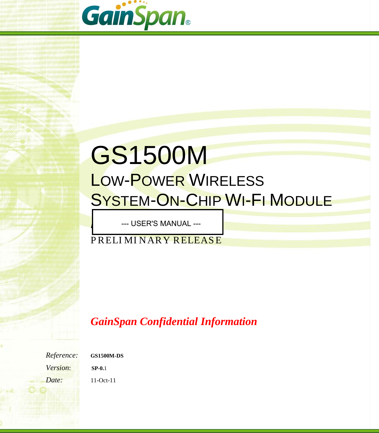
![GS1500M DATA SHEET PRELIMINARY GAINSPAN CONFIDENTIAL PAGE 7 OF 43 1 Overview 1.1 Document Overview HIS DOCUMENT describes the GS1500M Low Power module hardware specification. The GS1500M module provides a cost effective, low power, and flexible platform to add Wi-Fi® connectivity for embedded devices for a variety of applications, such as wireless sensors and thermostats. It combines ARM7-based processors with an RF transceiver, 802.11 MAC, security, & PHY functions, FLASH and SRAM, onboard and off module certified antenna options, and various RF front end options for end customer range needs in order to provide a WiFi and regulatory certified IEEE 802.11 radio with concurrent application processing services for variety of applications, while leverage existing 802.11 [1] wireless network infrastructures. 1.2 Product Overview ► Family of modules with different antenna and output power options: • GS1500M 1.450 inches by 0.900 inches by 0.143 inches (Length * Width * Height) 48-pin Dual Flat pack PCB Surface Mount Package. • Simple API for embedded markets covering large areas of applications ► Compliant with IEEE 802.11and regulatory domains: • Fully compatible with IEEE 802.11b/g/n. o DSSS modulation for data rate of 1 Mb/s and 2 Mb/s; CCK modulation rates of 5.5 and 11 Mb/s. o OFDM modulation for data rates of 6, 9, 12, 18, 24, 36, 48 and 54 Mb/s. o 802.11n 1x1 HT20 for data rates of MCS0 – 7. • Supports short preamble and short slot times. • WiFi Certified Solution o Supports 802.11i security WPA™ - Enterprise, Personal WPA2™ - Enterprise, Personal Vendor EAP Type(s) • EAP-TTLS/MSCHAPv2, PEAPv0/EAP-MSCHAPv2, PEAPv1/EAP-GTC, EAP-FAST, EAP-TLS • Hardware encryption/decryption engines for WEP, WPA/WPA2 (AES and TKIP) • RoHS and CE compliant • FCC/IC Certified - TBD ► Dual ARM7 Processor Platform: • 1st ARM7 processor (WLAN CPU) for WLAN software • 2nd ARM7 (APP CPU) for networking software • Based on Advanced Microprocessor Bus Architecture (AMBA) system: o AMBA High-Speed Bus (AHB). o AMBA Peripheral Bus (APB). • On-chip WLAN boot code located in dedicated boot ROM. T](https://usermanual.wiki/Gainspan/GS1500M/User-Guide-1581899-Page-7.png)
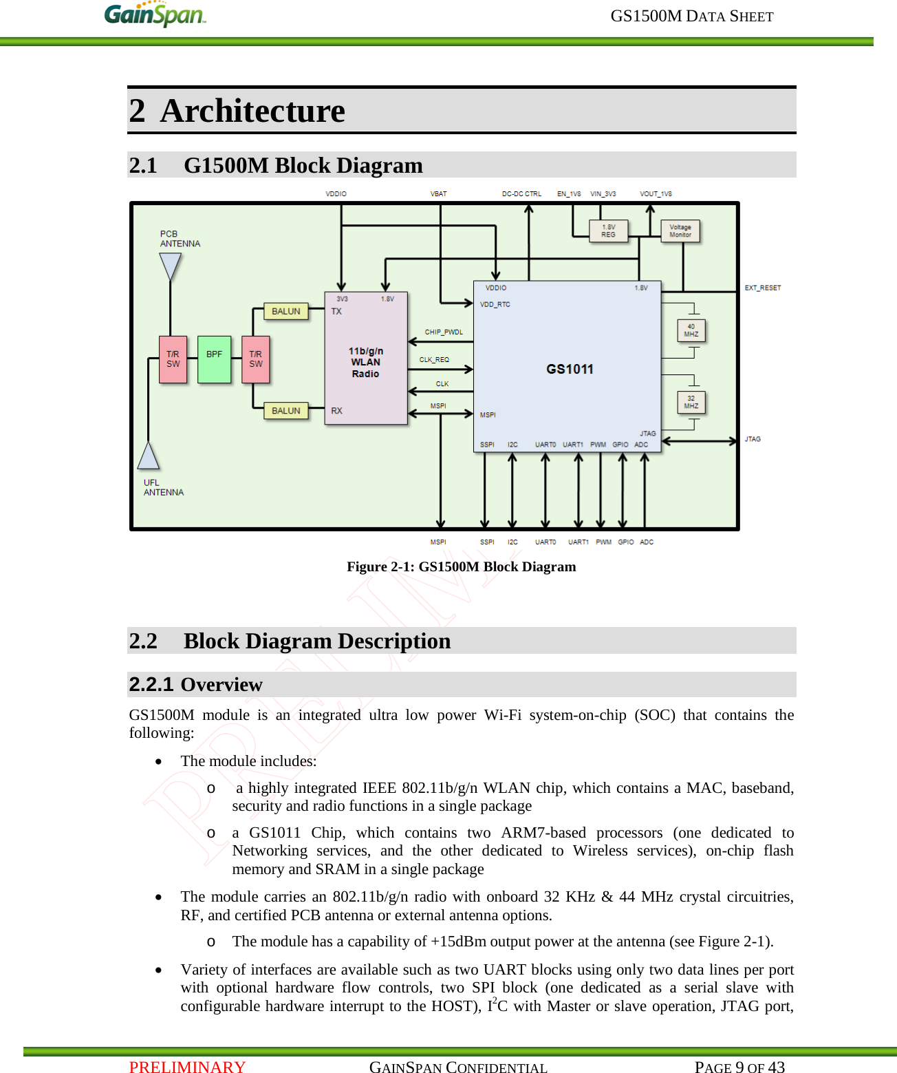
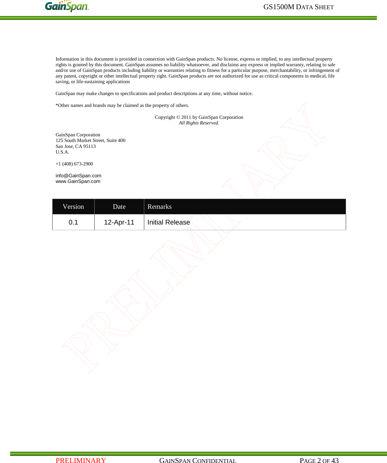
![GS1500M DATA SHEET PRELIMINARY GAINSPAN CONFIDENTIAL PAGE 10 OF 43 low-power 10-bit ADC capable of running at up to 32 KSamples/sec., GPIO’s, and LED Drivers/GPIO with 20mA capabilities. • GS1500M contains single power supply (VIN_3V3) with optional module controlled external regulator enable control pin (DC_DC_CNTL), a separate I/O supply (VDDIO) that can be tied to the HOST supply rail without the use of external voltage translators, Real Time Clock (RTC) with battery supply monitor option (VBAT), and two external alarm inputs enable wake-up of the system on external events & outputs (ALARM and RTC_OUT) to enable periodic wake-up of the remainder of the system. o The Module carries onboard single supply monitor for under voltage supply and onboard 1.8V regulator with enable/disable capabilities for power critical applications. 2.2.2 Wireless LAN and System Control Subsystem The GS1011 Wireless LAN and system control subsystem consists of an ARM7 TDMI-S CPU providing system control functions which provides for control and management functions of the external 802.11b/g/n WLAN chip. 2.2.3 Network Services Subsystem 2.2.3.1 APP CPU The Network services subsystem consists of an APP CPU which is based on an ARM7 TDMI-S core. It incorporates an AHB interface and a JTAG debug interface. The network RTOS, network stack, and customer application code can reside on this CPU. For more information, consult the GS1011 Peripheral and Register Description [2] and GS1011 IC data sheet [3] for detailed descriptions. 2.2.4 Memory Subsystem 2.2.4.1 Overview The GS1011 Chip contains several memory blocks: ► Boot ROM blocks. ► The software contained in this ROM provides the capability to download new firmware via the SPI Slave or UART interfaces and to control the update of WLAN and APP Flash Memory. ► 384 Kbytes of Embedded Flash to store program code. ► Three embedded Flash blocks of 128K bytes each ► WLAN Flash (contains the wireless LAN and system control subsystem software) ► APP Flash 0 and 1 (contain the Network/Application Software) ► 128 Kbytes of RAM shared between the two integrated CPU’s. ► 512 bytes of RTC memory ((retains data in all states, as long as the battery or other voltage supply is present) For more information, consult the GS1011 Peripheral and Register Description [2] and GS1011 IC data sheet [3] for detailed descriptions.](https://usermanual.wiki/Gainspan/GS1500M/User-Guide-1581899-Page-10.png)
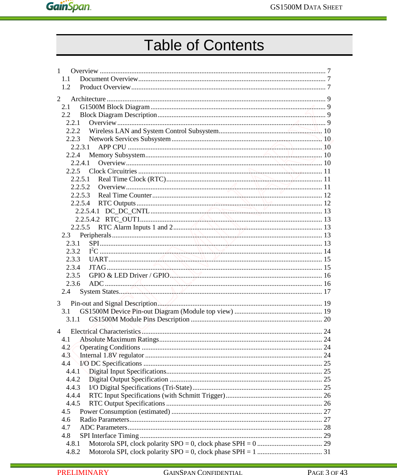
![GS1500M DATA SHEET PRELIMINARY GAINSPAN CONFIDENTIAL PAGE 12 OF 43 Figure 2-2: RTC Interface Diagram Resolution of the wake-up timer is one clock cycle, and, with onboard 32KHz. CLK, each 32bit effective register can provide up to 1.5 days worth of standby duration as the longest standby period. Polarity of the rtc_out1 pin is programmable. 2.2.5.3 Real Time Counter The Real Time Counter features: ► 48-bit length (with absolute duration dependent on the crystal frequency used). ► Low-power design. This counter is automatically reset by power-on-reset. This counter wraps around (returns to “all-0” once it has reached the highest possible “all-1” value). 2.2.5.4 RTC Outputs There are two RTC outputs (dc_dc_cntl and rtc_out1) that can be used to control external devices, such as sensors or voltage regulators. For more information, consult the GS1011 Peripheral and Register Description [2] and GS1011 IC data sheet [3] for detailed descriptions.](https://usermanual.wiki/Gainspan/GS1500M/User-Guide-1581899-Page-12.png)
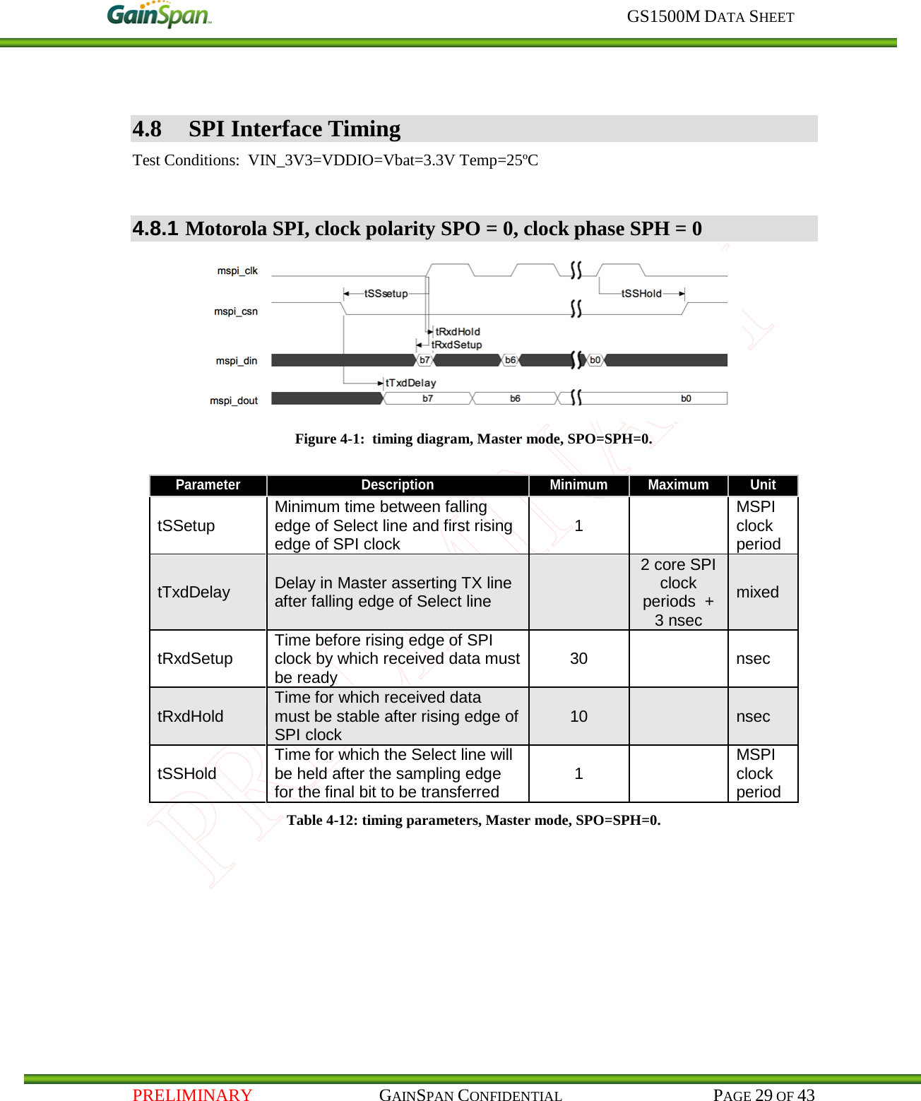
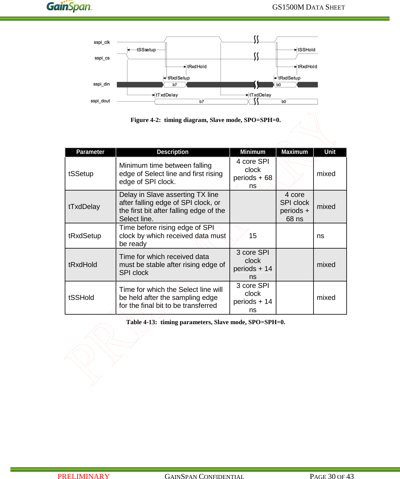
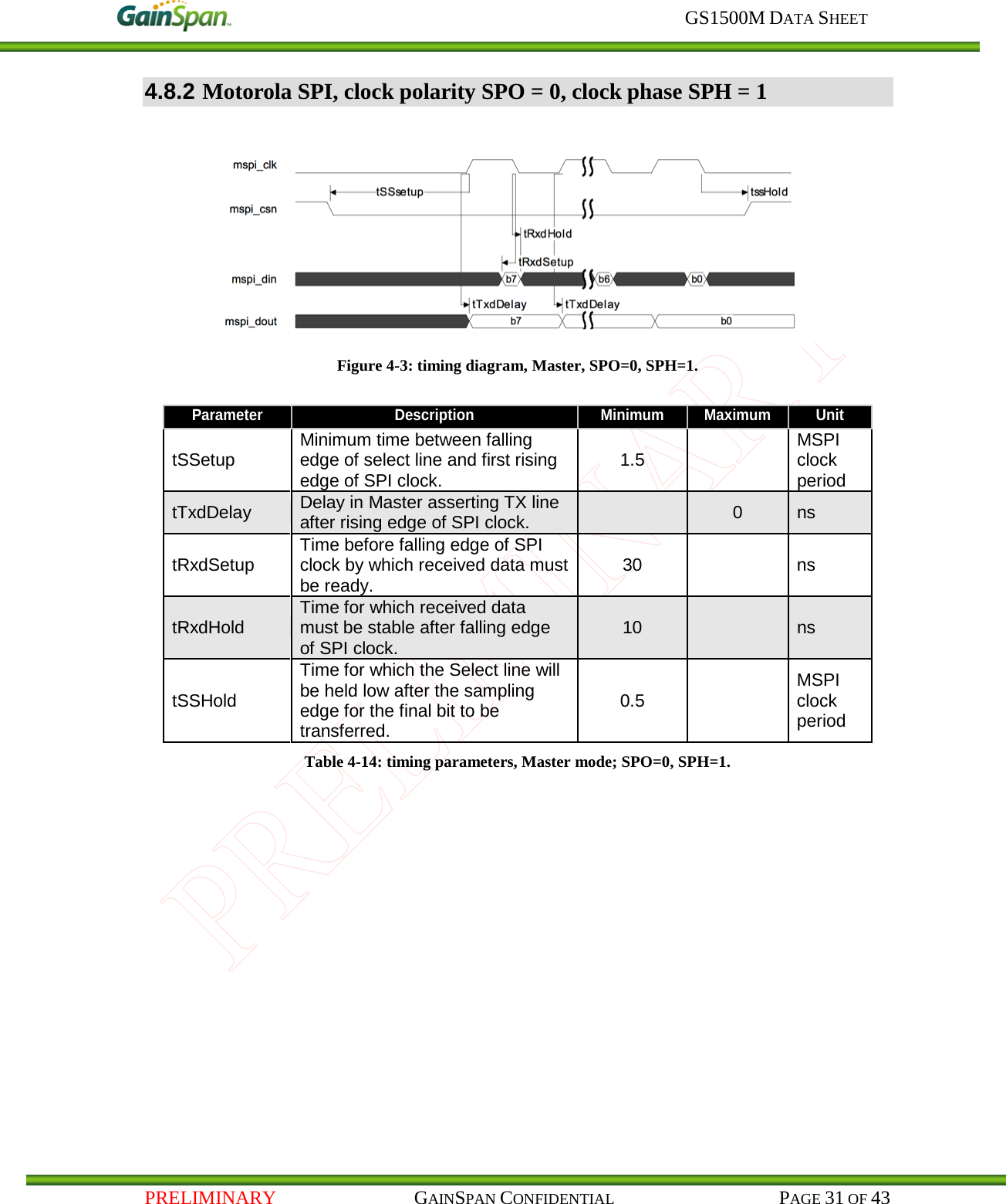
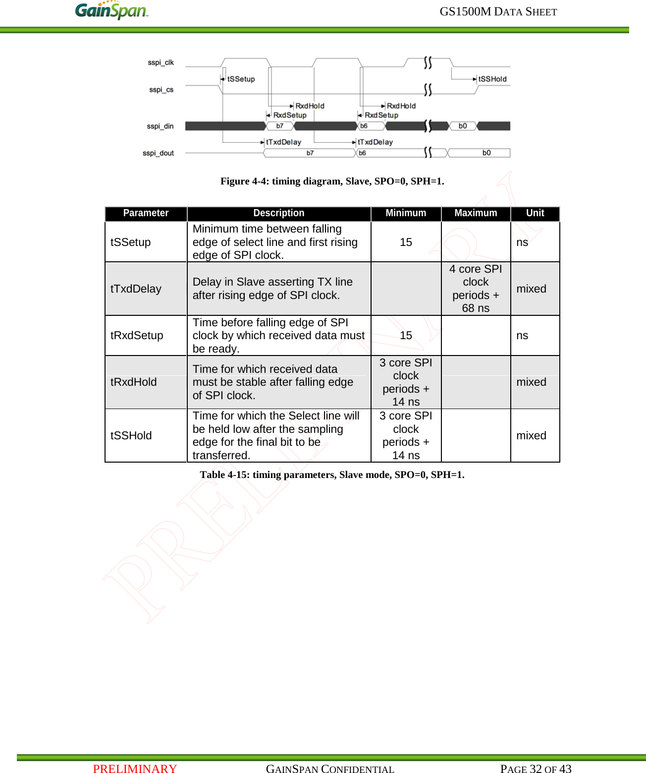
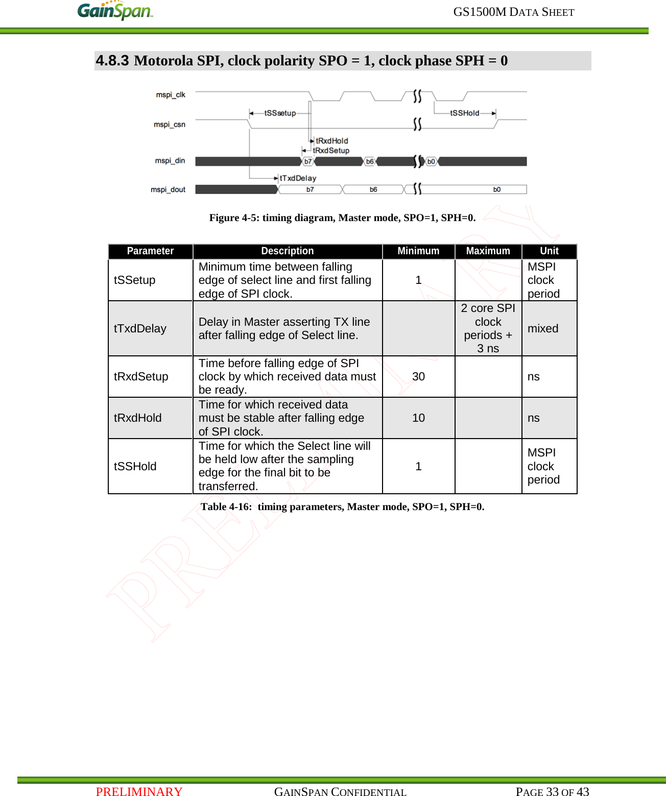
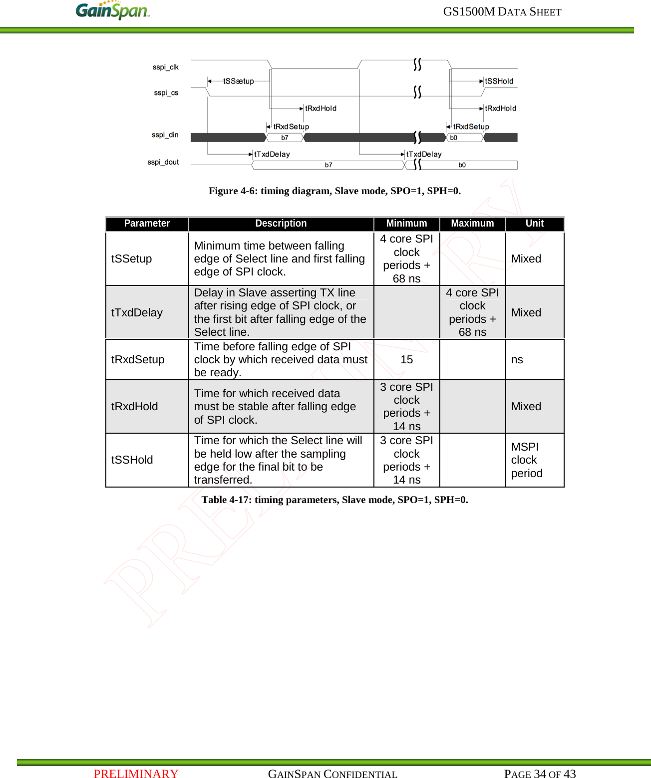
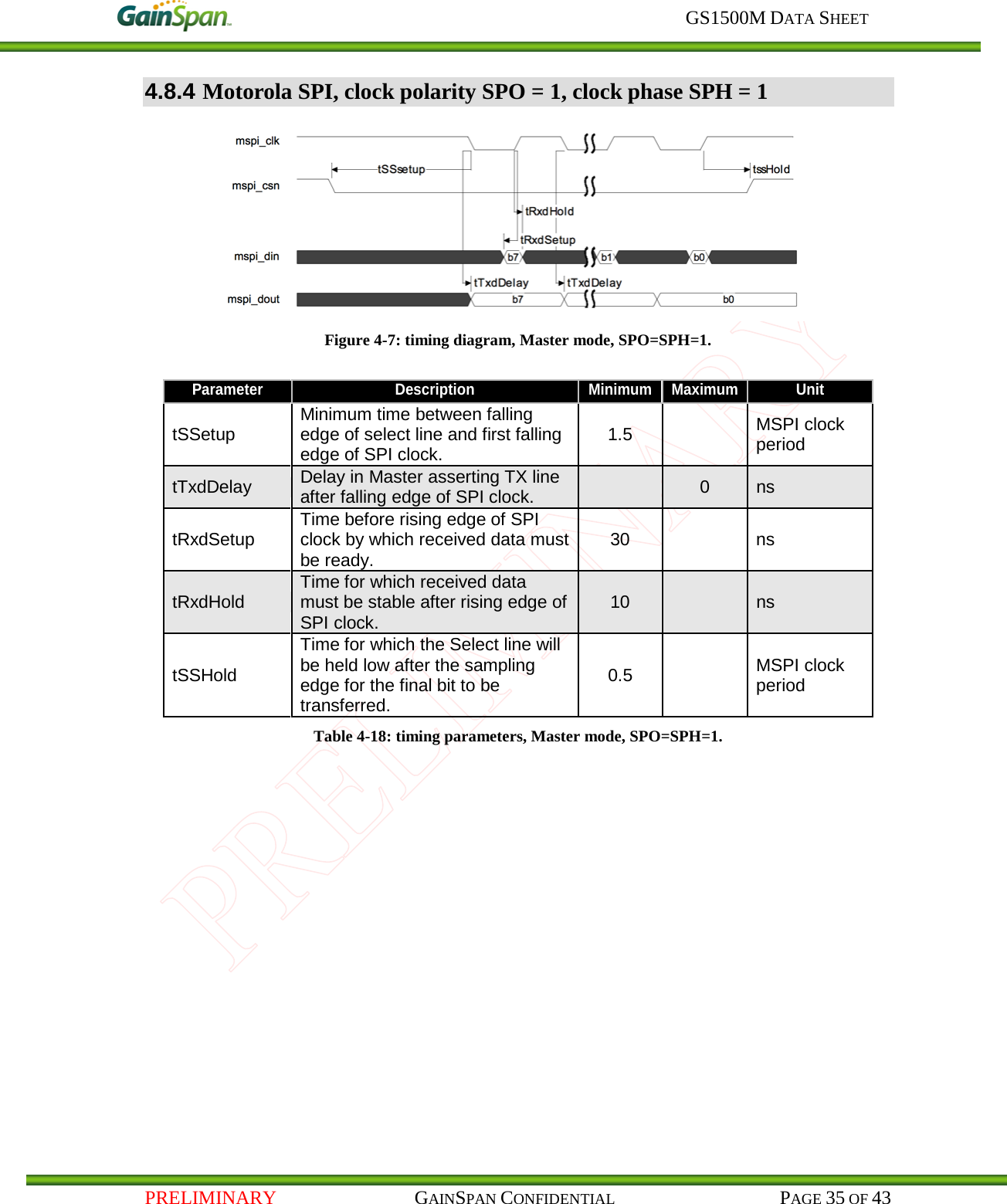
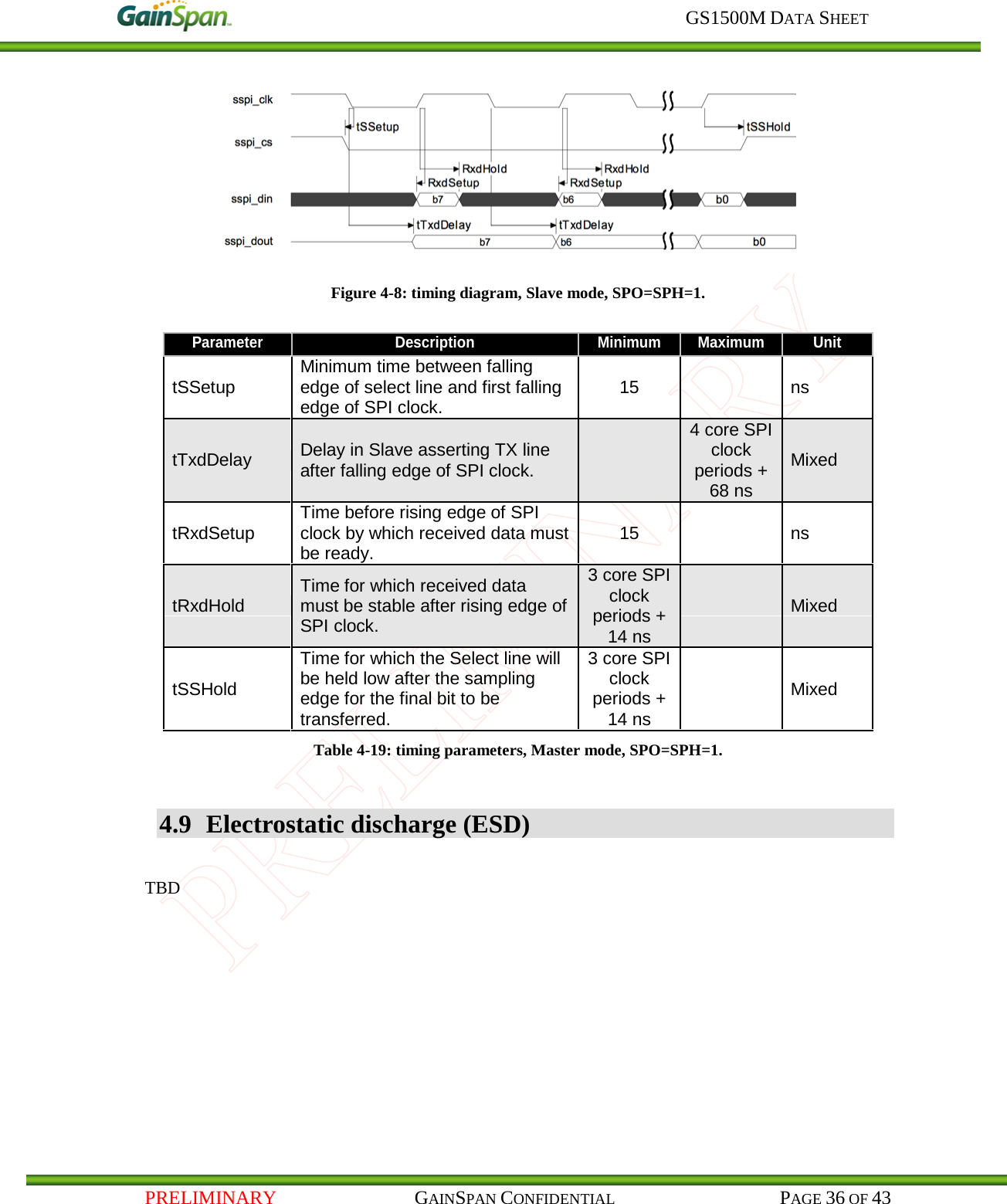
![GS1500M DATA SHEET PRELIMINARY GAINSPAN CONFIDENTIAL PAGE 13 OF 43 2.2.5.4.1 DC_DC_CNTL During Power-on-Reset (e.g. when the battery is connected), the dc_dc_cntl pin is held low; it goes high to indicate completion of RTC power-on-reset. This pin can be used as an enable into an external device such as voltage regulator. For more information, consult the GS1011 Peripheral and Register Description [2] and GS1011 IC data sheet [3] for detailed descriptions. 2.2.5.4.2 RTC_OUT1 The rtc_out1 signal can be disabled or driven by the Wake-up Counter 2. This counter is 34 bits long, and operates in the same fashion as Wake-up Counter 1. The rtc_out1 signal can be configured to output the low-power crystal oscillator clock (i.e. the 32 kHz clock) instead of a simple state transition. Wake-up Counter 2 is automatically reset at Power-on-Reset. For more information, consult the GS1011 Peripheral and Register Description [2] and GS1011 IC data sheet [3] for detailed descriptions. 2.2.5.5 RTC Alarm Inputs 1 and 2 The RTC inputs alarm1 and alarm2 operate as follows: ► dc_dc_cntl is set to “1” (typically enabling the power supply to the rest of the GS1011) whenever either of these inputs changes state. ► The RTC counter value is stored each time either of these inputs changes state. The inputs alarm1 and alarm2 have programmable polarity. Their task is to wake up the system (by setting dc_dc_cntl output pin to “1”) when an external event occurs. For more information, consult the GS1011 Peripheral and Register Description [2] and GS1011 IC data sheet [3] for detailed descriptions. 2.3 Peripherals Note: For register identification and additional details on the use of shared peripherals, refer to the GS1011 Peripheral and Register Description [3]. 2.3.1 SPI There are two general-purpose SPI interfaces (each configurable as master or slave) for external sensors, memory, or external CPU interface; one interface may be configured as a high-speed Slave-only. The master SPI block provides dual synchronous serial communication interfaces. The Master SPI block can be used in one of two modes of operations: as a serial master or a serial slave. Each block provides synchronous serial communication with slave or master devices, using one of the following protocols: ► Motorola Serial Peripheral Interface (SPI). ► Texas Instruments Synchronous Serial Protocol (SSP). ► National Semiconductor Microwire Protocol. Only Motorola Serial Peripheral Interface (SPI) timing is shown in this data sheet; however, National Semiconductor Microwire Protocol or Texas Instruments Synchronous Serial Protocol (SSP) modes are certainly supported. The SPI interface can also be used to access non-volatile external memory, such as an EEPROM block. The interface uses the SPI master mode to allow easy connection to industry-standard EEPROMs. The shared SPI blocks provide the following general features: ► 32-bit AMBA APB interface to allow access to data, control, and status information by the host processor. ► Full-duplex serial-master or serial-slave operation.](https://usermanual.wiki/Gainspan/GS1500M/User-Guide-1581899-Page-13.png)
![GS1500M DATA SHEET PRELIMINARY GAINSPAN CONFIDENTIAL PAGE 14 OF 43 ► Two clock design: • APB bus clock for bus interface and registers. • Serial input clock for core logic. ► Support of external EEPROM or other non-volatile memory. ► Programmable choice of Motorola SPI, Texas Instruments Synchronous Serial Protocol or National Semiconductor Microwire. ► Programmable control of the serial bit rate of the data transfer in serial-master mode of operation. ► Programmable phase and polarity of the bit rate clock. ► Programmable transfer modes to perform transmit and receive, transmit only, receive only and EEPROM read transfers. ► Programmable data word size (8, 16, 24 & 32 bits) for each data transfer. ► Transmit and receive FIFO buffer depth 8 words (of the selected size). ► Configurable number of slave select outputs in serial-master mode of operation: 1 to 4 serial slave-select output signals can be generated. ► Combined interrupt line with independent masking of interrupts. ► Transmit FIFO overflow, transmit FIFO empty, transmit FIFO underflow, receive FIFO full, receive FIFO underflow, receive FIFO overflow, and receive FIFO timeout interrupts. ► Transmit FIFO empty and receive FIFO full interrupts provide programmable threshold values. Both SPI blocks are configured to provide a FIFO depth of four entries. The SPI master interface can be used to access external sensor devices, and EEPROM containing system parameters, under software control while the SPI slave interface can be used to provide control of the GS1500M from an external CPU. SPI chip select (MPSISI_CS0 or MPSI_CS1) signals frame each data word. If the chip select is required to remain asserted for multiple data words, then a GPIO pin should be used for the chip select instead of the SPI chip select signals. For clock architecture and rates, please refer to section 7.1 Clock Architecture of GS1011 Peripheral and Register Description [2]. For other SPI Interface Timing, please refer to section 4.7. 2.3.2 I2C The I2C block provides a two-wire I2C serial interface. It provides the following features: ► 32-bit AMBA APB interface to allow access to data, control, and status Information by the host processor. ► Serial 2-wire I2C bus, compliant to the I2C Bus Specification Version 2.1. ► Supports only one transfer in Standard mode (100 Kb/s) and fast speed mode with a bit rate of up to 392 Kb/s. ► Supports Multi-Master System Architecture through I2C bus SCL line Synchronization and Arbitration. ► Transmitter and Receiver: The I2C block can act as the Transmitter or Receiver depending on the operation being performed. ► Master or slave I2C operation. ► 7- or 10-bit addressing.](https://usermanual.wiki/Gainspan/GS1500M/User-Guide-1581899-Page-14.png)
![GS1500M DATA SHEET PRELIMINARY GAINSPAN CONFIDENTIAL PAGE 15 OF 43 ► Ignores CBUS addresses (an older ancestor of I2C that used to share the I2C bus). ► Interrupt or polled mode operation. ► Combined interrupt line triggered by: • Tx FIFO not FULL. • Rx FIFO not EMPTY. • Rx FIFO FULL (can be used to transfer data by host interface in bursts). • Tx FIFO EMPTY (can be used to transfer data by host interface in bursts). • Rx FIFO OVER RUN. • Master mode to Slave Transfer Request. • Slave Transmit Request. • Break Interrupt (master mode): No Acknowledge received from slave for slave address or write data. ► Digital debounce logic for the received SDA and SCL lines. ► Hold Delay Insertion on SDA line. 2.3.3 UART The GS1500M includes two UART blocks. Each UART block provides an asynchronous communication interface, using only two data lines: Rx data and Tx data. Hardware flow control using RTS/CTS signaling is provided as an option. The UART is a standard asynchronous serial interface, 16450/16550 compatible. It provides the following features: ► Operation in full-duplex mode. ► All standard bit rates up to 921.6 kbps are supported. ► RTS/CTS flow control handshake (standard 16550 approach). ► 5, 6, 7 and 8-bit character format. ► 1 or 2 stop bits (1.5 in case of a 5-bit character format). ► Parity bit: none, even, odd, mark, or space. ► 16-byte Rx and 16-byte Tx FIFOs. The UART Serial port can be used to communicate with a PC or other devices, for debug or additional functionality. 2.3.4 JTAG The JTAG ports facilitate debugging of the board and system designs. This block has the following features: ► Compliant to IEEE-1149.1 TAP ports. ► One JTAG boundary scan TAP port. ► One set of JTAG pins, which support the following mode of operation: • APP ARM7TDMI-S Debug Mode. A detailed example of JTAG debug access is described in GainSpan Application Note AN-011 [4].](https://usermanual.wiki/Gainspan/GS1500M/User-Guide-1581899-Page-15.png)
![GS1500M DATA SHEET PRELIMINARY GAINSPAN CONFIDENTIAL PAGE 16 OF 43 2.3.5 GPIO & LED Driver / GPIO The GPIO ports are referenced to VDDIO. Two GPIO pins called GPIO30_LED1 & GPO31_LED2 have the capability to sink/source 20 mA typical (VDDIO=3.3V) to connect to devices such as switch contacts or LEDs. I2C_DATA/GPIO8 & I2C_CLK/GPIO9 have the capability to sink/source 12 mA typical (VDDIO=3.3V). Other GPIO’s have the capability to sink/source 4 mA typical (VDDIO=3.3V). All inputs are capable of generating processor interrupts. They can be individually programmed to provide edge- or level-triggered interrupts. For details on configuring GPIO ports, refer to the GS1011 Peripheral and Register Description [2]. 2.3.6 ADC The ADC is a 10-bit, low-power, A-to-D converter capable of running at up to 32 ksps. The ADC contains an internal band-gap reference which provides a stable 1.2 V reference voltage. The ADC can be programmed to use the 1.8 V supply as the full-scale reference. The ADC uses an input clock with a maximum frequency of 1 MHz. A conversion requires 32 clock cycles. When the internal band-gap reference is used, the reported integer Value at temperature T (ºC) is related to the voltage Vactual at the input pin as: Vactual=Value 1.2444 −0.00014 25 −T( )1023 When the 1.8V supply voltage is used as the reference, the corresponding relation is: Vactual =Value VDD,ADC −0.0361023 To reduce power consumption the ADC can be disabled automatically between periodic measurements and after single measurements. For more information, consult the GS1011 Peripheral and Register Description [2] and GS1011 IC data sheet [3] for detailed descriptions.](https://usermanual.wiki/Gainspan/GS1500M/User-Guide-1581899-Page-16.png)
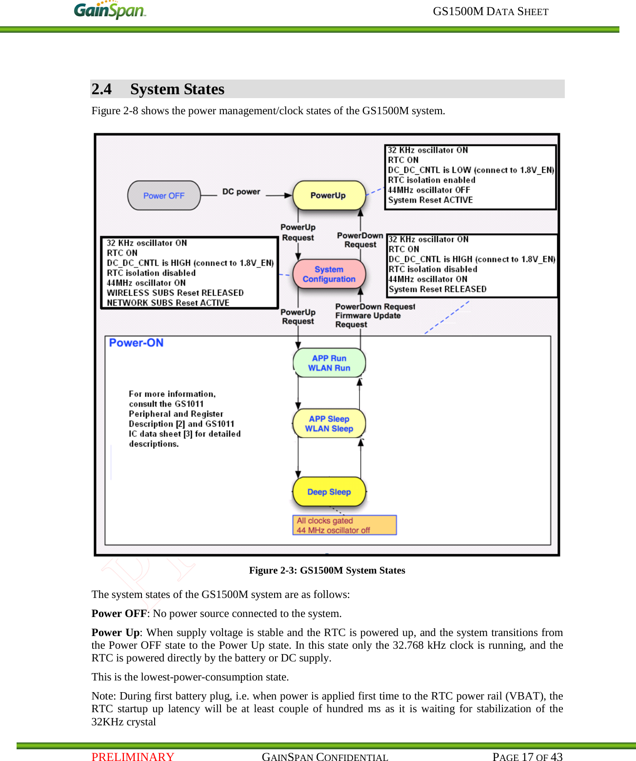
![GS1500M DATA SHEET PRELIMINARY GAINSPAN CONFIDENTIAL PAGE 18 OF 43 System Configuration: When a power-up is requested, the system transitions from the Power Up state to the System Configuration state. In this state, the WLAN CPU is released from reset by the RTC. The APP CPU remains in the reset state during System Configuration. The WLAN CPU then executes the required system configurations, releases the APP CPU from reset, and transitions to the Power-ON state. The System Configuration state is also entered on transition from the Power-ON state to the Power Up state, to complete necessary preparations before shutting off the power to the core system. Finally, the System Configuration state is used for firmware updates. Power-ON: This is the active state where all system components can be running. The Power-ON state has various sub-states, in which unused parts of the system can be in sleep mode, reducing power consumption. Sleep states are implemented by gating the clock signal off for a specific system component. The Deep-Sleep sub-state, in which all clocks are gated off, allows minimum power consumption while permitting rapid resumption of normal operation. In this state, the 44 MHz reference oscillator can be turned off to further reduce power consumption. For more information, consult the GS1011 Peripheral and Register Description [2] and GS1011 IC data sheet [3] for detailed descriptions.](https://usermanual.wiki/Gainspan/GS1500M/User-Guide-1581899-Page-18.png)
![GS1500M DATA SHEET PRELIMINARY GAINSPAN CONFIDENTIAL PAGE 43 OF 43 9 References [[11]] Title Wireless LAN Medium Access Control (MAC) and Physical Layer (PHY) Specifications Reference IEEE Standard 802.11-2007 Version Date June 12, 2007 Source IEEE [[22]] Title GS1011 Peripheral and Register Description Reference GS1011-PRD Version 1.0 Date November 11, 2009 Source GainSpan [[33]] Title GS1011 ULTRA LOW-POWER WIRELESS SYSTEM-ON-CHIP DATA SHEET Reference GS1011-DS Version 1.0 Date November 9, 2009 Source GainSpan](https://usermanual.wiki/Gainspan/GS1500M/User-Guide-1581899-Page-43.png)