Gainspan GS1500M LOW POWER WI-FI MODULE User Manual GS1011 Data sheet
Gainspan Corporation LOW POWER WI-FI MODULE GS1011 Data sheet
Gainspan >
Users Manual

GS1500M
LOW-POWER WIRELESS
SYSTEM-ON-CHIP WI-FI MODULE
DATA SHEET
PRELIMINARY RELEASE
GainSpan Confidential Information
Reference: GS1500M-DS
Version: SP-0.1
Date: 11-Oct-11
USER MANUAL
- USER MANUAL
USER'S MANUAL

GS1500M DATA SHEET
PRELIMINARY GAINSPAN CONFIDENTIAL PAGE 2 OF 43
Information in this document is provided in connection with GainSpan products. No license, express or implied, to any intellectual property
rights is granted by this document. GainSpan assumes no liability whatsoever, and disclaims any express or implied warranty, relating to sale
and/or use of GainSpan products including liability or warranties relating to fitness for a particular purpose, merchantability, or infringement of
any patent, copyright or other intellectual property right. GainSpan products are not authorized for use as critical components in medical, life
saving, or life-sustaining applications
GainSpan may make changes to specifications and product descriptions at any time, without notice.
*Other names and brands may be claimed as the property of others.
Copyright © 2011 by GainSpan Corporation
All Rights Reserved.
GainSpan Corporation
125 South Market Street, Suite 400
San Jose, CA 95113
U.S.A.
+1 (408) 673-2900
info@GainSpan.com
www.GainSpan.com
Version Date Remarks
0.1 12-Apr-11 Initial Release

GS1500M DATA SHEET
PRELIMINARY GAINSPAN CONFIDENTIAL PAGE 3 OF 43
Table of Contents
1 Overview ................................................................................................................................. 7
1.1 Document Overview ........................................................................................................... 7
1.2 Product Overview ............................................................................................................... 7
2 Architecture ............................................................................................................................. 9
2.1 G1500M Block Diagram .................................................................................................... 9
2.2 Block Diagram Description ................................................................................................ 9
2.2.1 Overview ....................................................................................................................... 9
2.2.2 Wireless LAN and System Control Subsystem ........................................................... 10
2.2.3 Network Services Subsystem ...................................................................................... 10
2.2.3.1 APP CPU ............................................................................................................... 10
2.2.4 Memory Subsystem ..................................................................................................... 10
2.2.4.1 Overview ................................................................................................................ 10
2.2.5 Clock Circuitries ......................................................................................................... 11
2.2.5.1 Real Time Clock (RTC) ......................................................................................... 11
2.2.5.2 Overview ................................................................................................................ 11
2.2.5.3 Real Time Counter ................................................................................................. 12
2.2.5.4 RTC Outputs .......................................................................................................... 12
2.2.5.4.1 DC_DC_CNTL .................................................................................................. 13
2.2.5.4.2 RTC_OUT1........................................................................................................ 13
2.2.5.5 RTC Alarm Inputs 1 and 2 ..................................................................................... 13
2.3 Peripherals ........................................................................................................................ 13
2.3.1 SPI ............................................................................................................................... 13
2.3.2 I2C ............................................................................................................................... 14
2.3.3 UART .......................................................................................................................... 15
2.3.4 JTAG ........................................................................................................................... 15
2.3.5 GPIO & LED Driver / GPIO ....................................................................................... 16
2.3.6 ADC ............................................................................................................................ 16
2.4 System States .................................................................................................................... 17
3 Pin-out and Signal Description .............................................................................................. 19
3.1 GS1500M Device Pin-out Diagram (Module top view) .................................................. 19
3.1.1 GS1500M Module Pins Description ........................................................................... 20
4 Electrical Characteristics ....................................................................................................... 24
4.1 Absolute Maximum Ratings ............................................................................................. 24
4.2 Operating Conditions ....................................................................................................... 24
4.3 Internal 1.8V regulator ..................................................................................................... 24
4.4 I/O DC Specifications ...................................................................................................... 25
4.4.1 Digital Input Specifications ......................................................................................... 25
4.4.2 Digital Output Specification ....................................................................................... 25
4.4.3 I/O Digital Specifications (Tri-State) .......................................................................... 25
4.4.4 RTC Input Specifications (with Schmitt Trigger) ....................................................... 26
4.4.5 RTC Output Specifications ......................................................................................... 26
4.5 Power Consumption (estimated) ...................................................................................... 27
4.6 Radio Parameters .............................................................................................................. 27
4.7 ADC Parameters ............................................................................................................... 28
4.8 SPI Interface Timing ........................................................................................................ 29
4.8.1 Motorola SPI, clock polarity SPO = 0, clock phase SPH = 0 ..................................... 29
4.8.2 Motorola SPI, clock polarity SPO = 0, clock phase SPH = 1 ..................................... 31

GS1500M DATA SHEET
PRELIMINARY GAINSPAN CONFIDENTIAL PAGE 4 OF 43
4.8.3 Motorola SPI, clock polarity SPO = 1, clock phase SPH = 0 ..................................... 33
4.8.4 Motorola SPI, clock polarity SPO = 1, clock phase SPH = 1 ..................................... 35
4.9 Electrostatic discharge (ESD) .......................................................................................... 36
5 Package and Layout Guidelines ............................................................................................ 37
5.1 GS1500M Recommended PCB Footprint and Dimensions ............................................. 37
6 Ordering Information ............................................................................................................. 39
7 Regulatory Notes ................................................................................................................... 40
8 Limitations ............................................................................................................................. 42
9 References ............................................................................................................................. 43

GS1500M DATA SHEET
PRELIMINARY GAINSPAN CONFIDENTIAL PAGE 5 OF 43
Figures
Figure 2-1: GS1500M Block Diagram ........................................................................................................ 9
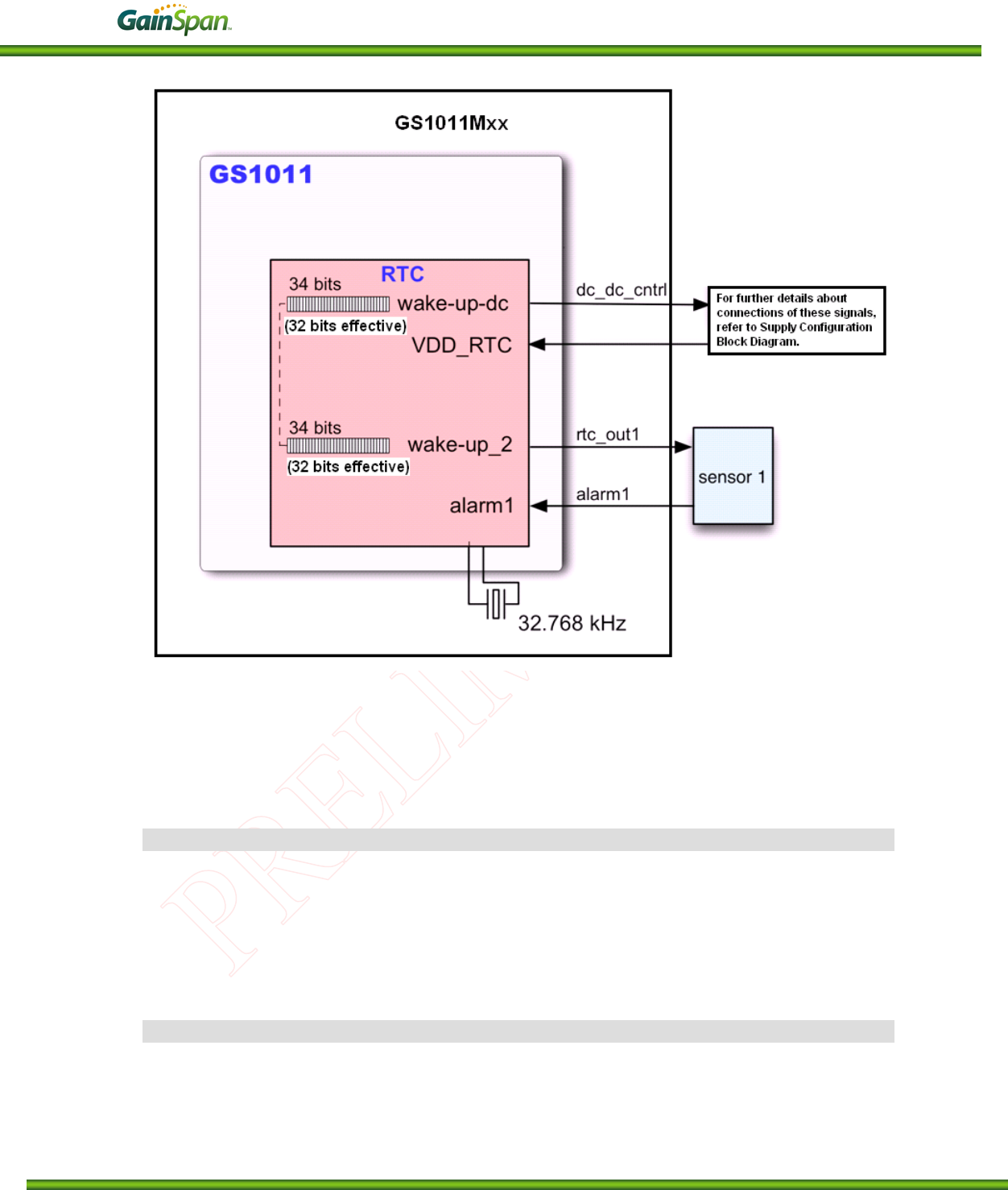
Figure 2-2: RTC Interface Diagram .......................................................................................................... 12
Figure 2-3: GS1500M System States ........................................................................................................ 17
Figure 3-1: GS1500M Device Pin-out Diagram (Module top view) ......................................................... 19
Figure 3-2: Module pin connection diagram ............................................................................................. 23
Figure 4-1: timing diagram, Master mode, SPO=SPH=0. ........................................................................ 29
Figure 4-2: timing diagram, Slave mode, SPO=SPH=0. .......................................................................... 30
Figure 4-3: timing diagram, Master, SPO=0, SPH=1................................................................................ 31
Figure 4-4: timing diagram, Slave, SPO=0, SPH=1. ................................................................................. 32
Figure 4-5: timing diagram, Master mode, SPO=1, SPH=0. ..................................................................... 33
Figure 4-6: timing diagram, Slave mode, SPO=1, SPH=0. ....................................................................... 34
Figure 4-7: timing diagram, Master mode, SPO=SPH=1. ......................................................................... 35
Figure 4-8: timing diagram, Slave mode, SPO=SPH=1. ........................................................................... 36
Figure 5-1: GS1500M Module Recommended PCB Footprint (dimensions are in inches) ..................... 37
Figure 5-2: GS1500M Module Dimensions (in inches) ........................................................................... 38

GS1500M DATA SHEET
PRELIMINARY GAINSPAN CONFIDENTIAL PAGE 6 OF 43
Tables
Table 3-1: Signal Description .................................................................................................................... 22
Table 4-1: Absolute Maximum Ratings .................................................................................................... 24
Table 4-2: Operating Conditions ............................................................................................................... 24
Table 4-3: Internal 1.8V Regulator ........................................................................................................... 24
Table 4-4: Digital Input Parameters .......................................................................................................... 25
Table 4-5: Digital Output Parameters ........................................................................................................ 25
Table 4-6: I/O Digital Parameters ............................................................................................................. 26
Table 4-7: RTC Input Parameters .............................................................................................................. 26
Table 4-8: RTC Output Parameters ........................................................................................................... 26
Table 4-9: Power Consumption in Different States................................................................................... 27
Table 4-10: Radio Parameters ................................................................................................................... 27
Table 4-11: ADC Parameters .................................................................................................................... 28
Table 4-12: timing parameters, Master mode, SPO=SPH=0. ................................................................... 29
Table 4-13: timing parameters, Slave mode, SPO=SPH=0. ..................................................................... 30
Table 4-14: timing parameters, Master mode; SPO=0, SPH=1. ............................................................... 31
Table 4-15: timing parameters, Slave mode, SPO=0, SPH=1. .................................................................. 32
Table 4-16: timing parameters, Master mode, SPO=1, SPH=0................................................................ 33
Table 4-17: timing parameters, Slave mode, SPO=1, SPH=0. .................................................................. 34
Table 4-18: timing parameters, Master mode, SPO=SPH=1. ................................................................... 35
Table 4-19: timing parameters, Master mode, SPO=SPH=1. ................................................................... 36

GS1500M DATA SHEET
PRELIMINARY GAINSPAN CONFIDENTIAL PAGE 7 OF 43
1 Overview
1.1 Document Overview
HIS DOCUMENT describes the GS1500M Low Power module hardware specification. The GS1500M
module provides a cost effective, low power, and flexible platform to add Wi-Fi® connectivity for
embedded devices for a variety of applications, such as wireless sensors and thermostats. It combines
ARM7-based processors with an RF transceiver, 802.11 MAC, security, & PHY functions, FLASH and
SRAM, onboard and off module certified antenna options, and various RF front end options for end
customer range needs in order to provide a WiFi and regulatory certified IEEE 802.11 radio with
concurrent application processing services for variety of applications, while leverage existing 802.11 [1]
wireless network infrastructures.
1.2 Product Overview
► Family of modules with different antenna and output power options:
• GS1500M 1.450 inches by 0.900 inches by 0.143 inches (Length * Width * Height) 48-pin
Dual Flat pack PCB Surface Mount Package.
• Simple API for embedded markets covering large areas of applications
► Compliant with IEEE 802.11and regulatory domains:
• Fully compatible with IEEE 802.11b/g/n.
o DSSS modulation for data rate of 1 Mb/s and 2 Mb/s; CCK modulation rates of 5.5
and 11 Mb/s.
o OFDM modulation for data rates of 6, 9, 12, 18, 24, 36, 48 and 54 Mb/s.
o 802.11n 1x1 HT20 for data rates of MCS0 – 7.
• Supports short preamble and short slot times.
• WiFi Certified Solution
o Supports 802.11i security
WPA™ - Enterprise, Personal
WPA2™ - Enterprise, Personal
Vendor EAP Type(s)
• EAP-TTLS/MSCHAPv2, PEAPv0/EAP-MSCHAPv2, PEAPv1/EAP-
GTC, EAP-FAST, EAP-TLS
• Hardware encryption/decryption engines for WEP, WPA/WPA2 (AES and TKIP)
• RoHS and CE compliant
• FCC/IC Certified - TBD
► Dual ARM7 Processor Platform:
• 1st ARM7 processor (WLAN CPU) for WLAN software
• 2nd ARM7 (APP CPU) for networking software
• Based on Advanced Microprocessor Bus Architecture (AMBA) system:
o AMBA High-Speed Bus (AHB).
o AMBA Peripheral Bus (APB).
• On-chip WLAN boot code located in dedicated boot ROM.
T

GS1500M DATA SHEET
PRELIMINARY GAINSPAN CONFIDENTIAL PAGE 8 OF 43
► Interfaces:
• PCB or external antenna options.
• Two general-purpose SPI interfaces (each configurable as master or slave) for external
sensors, memory, or external CPU interface; one interface may be configured as a high-speed
Slave-only.
• Two multi-purpose UART interfaces.
• Up to 23 configure able general purpose I/Os.
• Single 3.3V supply option
o I/O supply voltage 1.8 ~ 3.3V option
• One PWM output
• I2C master/slave interface.
• Two 10-bit ADC channels, aggregate sample rate 32 kS/s.
• Two alarm inputs to asynchronously awaken the chip.
• Support of up to two control outputs for power supply and sensors.
► Embedded RTC (Real Time Clock) can run directly from battery.
► Power supply monitoring capability.
► Low-power mode operations
► Sleep and Deep Sleep
GS1500M DATA SHEET
PRELIMINARY GAINSPAN CONFIDENTIAL PAGE 9 OF 43
2 Architecture
2.1 G1500M Block Diagram
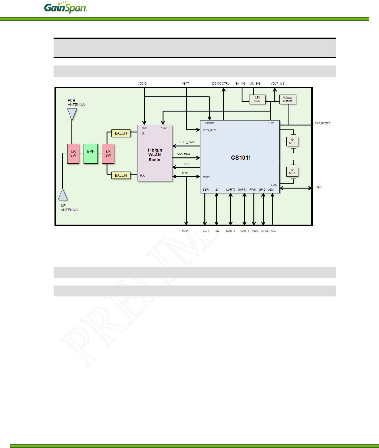
Figure 2-1: GS1500M Block Diagram
2.2 Block Diagram Description
2.2.1 Overview
GS1500M module is an integrated ultra low power Wi-Fi system-on-chip (SOC) that contains the
following:
• The module includes:
o a highly integrated IEEE 802.11b/g/n WLAN chip, which contains a MAC, baseband,
security and radio functions in a single package
o a GS1011 Chip, which contains two ARM7-based processors (one dedicated to
Networking services, and the other dedicated to Wireless services), on-chip flash
memory and SRAM in a single package
• The module carries an 802.11b/g/n radio with onboard 32 KHz & 44 MHz crystal circuitries,
RF, and certified PCB antenna or external antenna options.
o The module has a capability of +15dBm output power at the antenna (see Figure 2-1).
• Variety of interfaces are available such as two UART blocks using only two data lines per port
with optional hardware flow controls, two SPI block (one dedicated as a serial slave with
configurable hardware interrupt to the HOST), I2C with Master or slave operation, JTAG port,

GS1500M DATA SHEET
PRELIMINARY GAINSPAN CONFIDENTIAL PAGE 10 OF 43
low-power 10-bit ADC capable of running at up to 32 KSamples/sec., GPIO’s, and LED
Drivers/GPIO with 20mA capabilities.
• GS1500M contains single power supply (VIN_3V3) with optional module controlled external
regulator enable control pin (DC_DC_CNTL), a separate I/O supply (VDDIO) that can be tied to
the HOST supply rail without the use of external voltage translators, Real Time Clock (RTC)
with battery supply monitor option (VBAT), and two external alarm inputs enable wake-up of
the system on external events & outputs (ALARM and RTC_OUT) to enable periodic wake-up
of the remainder of the system.
o The Module carries onboard single supply monitor for under voltage supply and onboard
1.8V regulator with enable/disable capabilities for power critical applications.
2.2.2 Wireless LAN and System Control Subsystem
The GS1011 Wireless LAN and system control subsystem consists of an ARM7 TDMI-S CPU providing
system control functions which provides for control and management functions of the external
802.11b/g/n WLAN chip.
2.2.3 Network Services Subsystem
2.2.3.1 APP CPU
The Network services subsystem consists of an APP CPU which is based on an ARM7 TDMI-S core. It
incorporates an AHB interface and a JTAG debug interface. The network RTOS, network stack, and
customer application code can reside on this CPU. For more information, consult the GS1011 Peripheral
and Register Description [2] and GS1011 IC data sheet [3] for detailed descriptions.
2.2.4 Memory Subsystem
2.2.4.1 Overview
The GS1011 Chip contains several memory blocks:
► Boot ROM blocks.
► The software contained in this ROM provides the capability to download new firmware via
the SPI Slave or UART interfaces and to control the update of WLAN and APP Flash
Memory.
► 384 Kbytes of Embedded Flash to store program code.
► Three embedded Flash blocks of 128K bytes each
► WLAN Flash (contains the wireless LAN and system control subsystem software)
► APP Flash 0 and 1 (contain the Network/Application Software)
► 128 Kbytes of RAM shared between the two integrated CPU’s.
► 512 bytes of RTC memory ((retains data in all states, as long as the battery or other voltage supply
is present)
For more information, consult the GS1011 Peripheral and Register Description [2] and GS1011 IC data
sheet [3] for detailed descriptions.

GS1500M DATA SHEET
PRELIMINARY GAINSPAN CONFIDENTIAL PAGE 11 OF 43
2.2.5 Clock Circuitries
The GS1500M architecture uses a low-power oscillator (i.e. 32 kHz) to provide a minimal subset of
functions when the chip is in its low-power deep sleep mode, and a high-speed 44 MHz oscillator to
provide clock signals for the processors, bus, and interfaces during active operation. Intermediate modes
of operation, in which the 44 MHz oscillator is active but some modules are inactive, are obtained by
gating the clock signal to different subsystems. The Clock & Reset Controller, within the device, is
responsible for generation, selection and gating of the clocks used in the module to reduce power
consumption in various power states.
2.2.5.1 Real Time Clock (RTC)
2.2.5.2 Overview
To provide global time (and date) to the system, the GS1500M Chip is equipped with a low-power Real
Time Clock (RTC).
RTC key features include:
► 32.768 kHz crystal support.
► Two external alarm inputs to wake up the device.
► Two programmable periodic outputs (one for a DC/DC regulator and one for a sensor).
► Embedded 128x32 non-volatile (battery-powered) RAM.
► Embedded Power On Reset.
► Real Time Counter (48 bits; 46 bits effective).
An overview of RTC block diagram is shown in Figure 2-3. The RTC contains a low-power oscillator
that can use 32.768 kHz crystals. In normal operation the RTC is always powered up, even in the Power
Up state (see Figure 2-3).
Two programmable embedded alarm counters (wrap-around) are provided to enable periodic wake-up of
the remainder of the system, and one independent external component (typically a sensor). Two external
alarm inputs enable wake-up of the system on external events. The global times are recorded on each
external event and if the system is in the Power-ON state (see Figure 2-8), an interrupt is provided. The
RTC includes a Power-On Reset (POR) circuit, to eliminate the need for an external component. The
RTC contains low-leakage non-volatile (battery-powered) RAM, to enable storage of data that needs to
be preserved.
Total current consumption of the RTC in the worst case is typically less than 5 µA without data storage,
using the 32.768 kHz oscillator.
GS1500M DATA SHEET
PRELIMINARY GAINSPAN CONFIDENTIAL PAGE 12 OF 43
Figure 2-2: RTC Interface Diagram
Resolution of the wake-up timer is one clock cycle, and, with onboard 32KHz. CLK, each 32bit effective
register can provide up to 1.5 days worth of standby duration as the longest standby period. Polarity of
the rtc_out1 pin is programmable.
2.2.5.3 Real Time Counter
The Real Time Counter features:
► 48-bit length (with absolute duration dependent on the crystal frequency used).
► Low-power design.
This counter is automatically reset by power-on-reset.
This counter wraps around (returns to “all-0” once it has reached the highest possible “all-1” value).
2.2.5.4 RTC Outputs
There are two RTC outputs (dc_dc_cntl and rtc_out1) that can be used to control external devices, such
as sensors or voltage regulators. For more information, consult the GS1011 Peripheral and Register
Description [2] and GS1011 IC data sheet [3] for detailed descriptions.

GS1500M DATA SHEET
PRELIMINARY GAINSPAN CONFIDENTIAL PAGE 13 OF 43
2.2.5.4.1 DC_DC_CNTL
During Power-on-Reset (e.g. when the battery is connected), the dc_dc_cntl pin is held low; it goes high
to indicate completion of RTC power-on-reset. This pin can be used as an enable into an external device
such as voltage regulator. For more information, consult the GS1011 Peripheral and Register Description
[2] and GS1011 IC data sheet [3] for detailed descriptions.
2.2.5.4.2 RTC_OUT1
The rtc_out1 signal can be disabled or driven by the Wake-up Counter 2. This counter is 34 bits long,
and operates in the same fashion as Wake-up Counter 1. The rtc_out1 signal can be configured to output
the low-power crystal oscillator clock (i.e. the 32 kHz clock) instead of a simple state transition. Wake-
up Counter 2 is automatically reset at Power-on-Reset. For more information, consult the GS1011
Peripheral and Register Description [2] and GS1011 IC data sheet [3] for detailed descriptions.
2.2.5.5 RTC Alarm Inputs 1 and 2
The RTC inputs alarm1 and alarm2 operate as follows:
► dc_dc_cntl is set to “1” (typically enabling the power supply to the rest of the GS1011) whenever
either of these inputs changes state.
► The RTC counter value is stored each time either of these inputs changes state.
The inputs alarm1 and alarm2 have programmable polarity. Their task is to wake up the system (by
setting dc_dc_cntl output pin to “1”) when an external event occurs. For more information, consult the
GS1011 Peripheral and Register Description [2] and GS1011 IC data sheet [3] for detailed descriptions.
2.3 Peripherals
Note: For register identification and additional details on the use of shared peripherals, refer to the
GS1011 Peripheral and Register Description [3].
2.3.1 SPI
There are two general-purpose SPI interfaces (each configurable as master or slave) for external sensors,
memory, or external CPU interface; one interface may be configured as a high-speed Slave-only. The
master SPI block provides dual synchronous serial communication interfaces. The Master SPI block can
be used in one of two modes of operations: as a serial master or a serial slave. Each block provides
synchronous serial communication with slave or master devices, using one of the following protocols:
► Motorola Serial Peripheral Interface (SPI).
► Texas Instruments Synchronous Serial Protocol (SSP).
► National Semiconductor Microwire Protocol.
Only Motorola Serial Peripheral Interface (SPI) timing is shown in this data sheet; however, National
Semiconductor Microwire Protocol or Texas Instruments Synchronous Serial Protocol (SSP) modes are
certainly supported. The SPI interface can also be used to access non-volatile external memory, such as
an EEPROM block. The interface uses the SPI master mode to allow easy connection to industry-
standard EEPROMs.
The shared SPI blocks provide the following general features:
► 32-bit AMBA APB interface to allow access to data, control, and status information by the host
processor.
► Full-duplex serial-master or serial-slave operation.

GS1500M DATA SHEET
PRELIMINARY GAINSPAN CONFIDENTIAL PAGE 14 OF 43
► Two clock design:
• APB bus clock for bus interface and registers.
• Serial input clock for core logic.
► Support of external EEPROM or other non-volatile memory.
► Programmable choice of Motorola SPI, Texas Instruments Synchronous Serial Protocol or
National Semiconductor Microwire.
► Programmable control of the serial bit rate of the data transfer in serial-master mode of operation.
► Programmable phase and polarity of the bit rate clock.
► Programmable transfer modes to perform transmit and receive, transmit only, receive only and
EEPROM read transfers.
► Programmable data word size (8, 16, 24 & 32 bits) for each data transfer.
► Transmit and receive FIFO buffer depth 8 words (of the selected size).
► Configurable number of slave select outputs in serial-master mode of operation: 1 to 4 serial slave-
select output signals can be generated.
► Combined interrupt line with independent masking of interrupts.
► Transmit FIFO overflow, transmit FIFO empty, transmit FIFO underflow, receive FIFO full,
receive FIFO underflow, receive FIFO overflow, and receive FIFO timeout interrupts.
► Transmit FIFO empty and receive FIFO full interrupts provide programmable threshold values.
Both SPI blocks are configured to provide a FIFO depth of four entries.
The SPI master interface can be used to access external sensor devices, and EEPROM containing system
parameters, under software control while the SPI slave interface can be used to provide control of the
GS1500M from an external CPU.
SPI chip select (MPSISI_CS0 or MPSI_CS1) signals frame each data word. If the chip select is required
to remain asserted for multiple data words, then a GPIO pin should be used for the chip select instead of
the SPI chip select signals. For clock architecture and rates, please refer to section 7.1 Clock
Architecture of GS1011 Peripheral and Register Description [2]. For other SPI Interface Timing, please
refer to section 4.7.
2.3.2 I2C
The I2C block provides a two-wire I2C serial interface. It provides the following features:
► 32-bit AMBA APB interface to allow access to data, control, and status Information by the host
processor.
► Serial 2-wire I2C bus, compliant to the I2C Bus Specification Version 2.1.
► Supports only one transfer in Standard mode (100 Kb/s) and fast speed mode with a bit rate of up
to 392 Kb/s.
► Supports Multi-Master System Architecture through I2C bus SCL line Synchronization and
Arbitration.
► Transmitter and Receiver: The I2C block can act as the Transmitter or Receiver depending on the
operation being performed.
► Master or slave I2C operation.
► 7- or 10-bit addressing.

GS1500M DATA SHEET
PRELIMINARY GAINSPAN CONFIDENTIAL PAGE 15 OF 43
► Ignores CBUS addresses (an older ancestor of I2C that used to share the I2C bus).
► Interrupt or polled mode operation.
► Combined interrupt line triggered by:
• Tx FIFO not FULL.
• Rx FIFO not EMPTY.
• Rx FIFO FULL (can be used to transfer data by host interface in bursts).
• Tx FIFO EMPTY (can be used to transfer data by host interface in bursts).
• Rx FIFO OVER RUN.
• Master mode to Slave Transfer Request.
• Slave Transmit Request.
• Break Interrupt (master mode): No Acknowledge received from slave for slave address or
write data.
► Digital debounce logic for the received SDA and SCL lines.
► Hold Delay Insertion on SDA line.
2.3.3 UART
The GS1500M includes two UART blocks. Each UART block provides an asynchronous communication
interface, using only two data lines: Rx data and Tx data. Hardware flow control using RTS/CTS
signaling is provided as an option. The UART is a standard asynchronous serial interface, 16450/16550
compatible. It provides the following features:
► Operation in full-duplex mode.
► All standard bit rates up to 921.6 kbps are supported.
► RTS/CTS flow control handshake (standard 16550 approach).
► 5, 6, 7 and 8-bit character format.
► 1 or 2 stop bits (1.5 in case of a 5-bit character format).
► Parity bit: none, even, odd, mark, or space.
► 16-byte Rx and 16-byte Tx FIFOs.
The UART Serial port can be used to communicate with a PC or other devices, for debug or additional
functionality.
2.3.4 JTAG
The JTAG ports facilitate debugging of the board and system designs. This block has the following
features:
► Compliant to IEEE-1149.1 TAP ports.
► One JTAG boundary scan TAP port.
► One set of JTAG pins, which support the following mode of operation:
• APP ARM7TDMI-S Debug Mode.
A detailed example of JTAG debug access is described in GainSpan Application Note AN-011 [4].

GS1500M DATA SHEET
PRELIMINARY GAINSPAN CONFIDENTIAL PAGE 16 OF 43
2.3.5 GPIO & LED Driver / GPIO
The GPIO ports are referenced to VDDIO. Two GPIO pins called GPIO30_LED1 & GPO31_LED2 have
the capability to sink/source 20 mA typical (VDDIO=3.3V) to connect to devices such as switch contacts
or LEDs. I2C_DATA/GPIO8 & I2C_CLK/GPIO9 have the capability to sink/source 12 mA typical
(VDDIO=3.3V). Other GPIO’s have the capability to sink/source 4 mA typical (VDDIO=3.3V). All
inputs are capable of generating processor interrupts. They can be individually programmed to provide
edge- or level-triggered interrupts. For details on configuring GPIO ports, refer to the GS1011
Peripheral and Register Description [2].
2.3.6 ADC
The ADC is a 10-bit, low-power, A-to-D converter capable of running at up to 32 ksps. The ADC
contains an internal band-gap reference which provides a stable 1.2 V reference voltage. The ADC can
be programmed to use the 1.8 V supply as the full-scale reference. The ADC uses an input clock with a
maximum frequency of 1 MHz. A conversion requires 32 clock cycles.
When the internal band-gap reference is used, the reported integer Value at temperature T (ºC) is related
to the voltage Vactual at the input pin as:
V
actual
=Value 1.2444 −0.00014 25 −T
( )
1023
When the 1.8V supply voltage is used as the reference, the corresponding relation is:
Vactual =Value VDD,ADC −0.036
1023
To reduce power consumption the ADC can be disabled automatically between periodic measurements
and after single measurements.
For more information, consult the GS1011 Peripheral and Register Description [2] and GS1011 IC data
sheet [3] for detailed descriptions.
GS1500M DATA SHEET
PRELIMINARY GAINSPAN CONFIDENTIAL PAGE 17 OF 43
2.4 System States
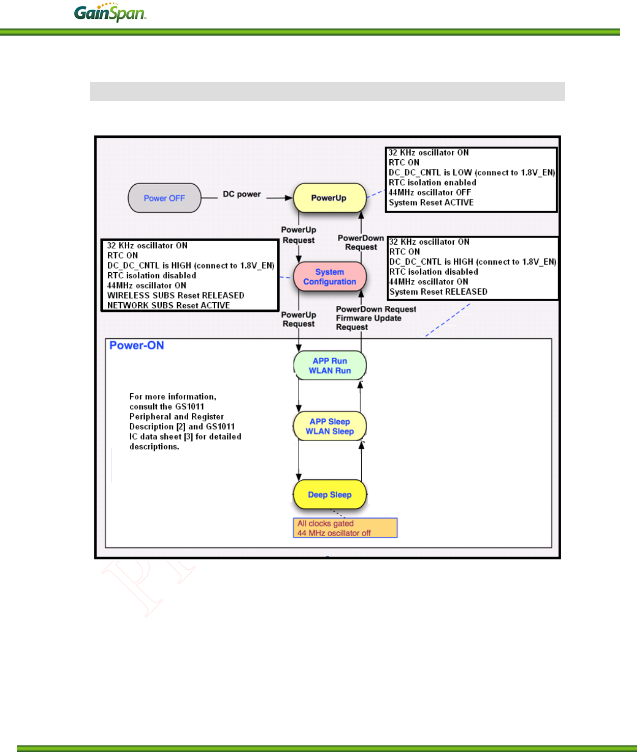
Figure 2-8 shows the power management/clock states of the GS1500M system.
Figure 2-3: GS1500M System States
The system states of the GS1500M system are as follows:
Power OFF: No power source connected to the system.
Power Up: When supply voltage is stable and the RTC is powered up, and the system transitions from
the Power OFF state to the Power Up state. In this state only the 32.768 kHz clock is running, and the
RTC is powered directly by the battery or DC supply.
This is the lowest-power-consumption state.
Note: During first battery plug, i.e. when power is applied first time to the RTC power rail (VBAT), the
RTC startup up latency will be at least couple of hundred ms as it is waiting for stabilization of the
32KHz crystal

GS1500M DATA SHEET
PRELIMINARY GAINSPAN CONFIDENTIAL PAGE 18 OF 43
System Configuration: When a power-up is requested, the system transitions from the Power Up state
to the System Configuration state. In this state, the WLAN CPU is released from reset by the RTC. The
APP CPU remains in the reset state during System Configuration. The WLAN CPU then executes the
required system configurations, releases the APP CPU from reset, and transitions to the Power-ON state.
The System Configuration state is also entered on transition from the Power-ON state to the Power Up
state, to complete necessary preparations before shutting off the power to the core system. Finally, the
System Configuration state is used for firmware updates.
Power-ON: This is the active state where all system components can be running. The Power-ON state
has various sub-states, in which unused parts of the system can be in sleep mode, reducing power
consumption. Sleep states are implemented by gating the clock signal off for a specific system
component. The Deep-Sleep sub-state, in which all clocks are gated off, allows minimum power
consumption while permitting rapid resumption of normal operation. In this state, the 44 MHz reference
oscillator can be turned off to further reduce power consumption.
For more information, consult the GS1011 Peripheral and Register Description [2] and GS1011 IC data
sheet [3] for detailed descriptions.
GS1500M DATA SHEET
PRELIMINARY GAINSPAN CONFIDENTIAL PAGE 19 OF 43
3 Pin-out and Signal Description
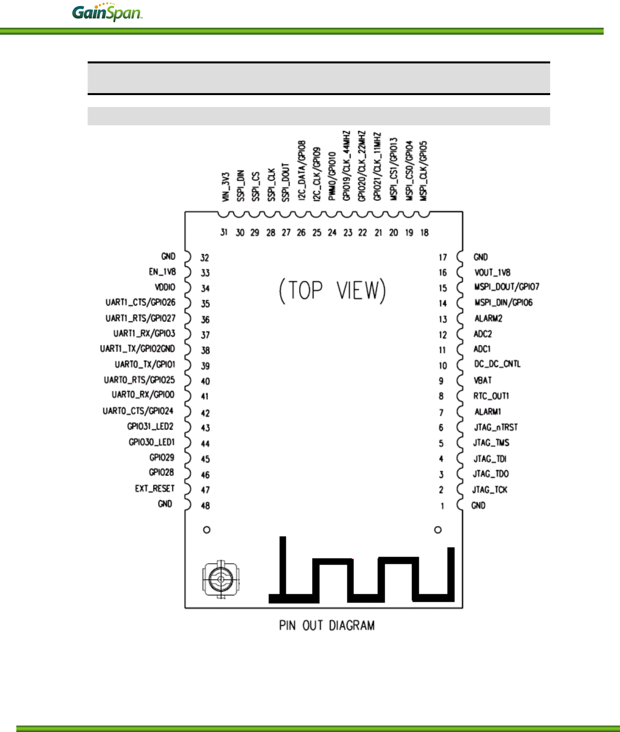
3.1 GS1500M Device Pin-out Diagram (Module top view)
Figure 3-1: GS1500M Device Pin-out Diagram (Module top view)
GS1500M DATA SHEET
PRELIMINARY GAINSPAN CONFIDENTIAL PAGE 20 OF 43
3.1.1 GS1500M Module Pins Description
Pins Name Voltage Domain Internal Bias after
hardware reset Signal State Description
1 GND 0V Not Applicable Analog port Ground
2 JTAG_TCK VDDIO Pull-up (See Note 1) Digital Input Joint Test Action Group Test Clock
3 JTAG_TDO VDDIO Not Applicable Digital Output Joint Test Action Group Test Data Out
4 JTAG_TDI VDDIO Pull-up (See Note 1) Digital Input Joint Test Action Group Test Data In
5 JTAG_TMS VDDIO Pull-up (See Note 1) Digital Input Joint Test Action Group Test Mode Select
6 JTAG_nTRST VDDIO Pull-up (See Note 1) Digital Input Joint Test Action Group Test Mode Reset
Active Low
7 ALARM1 VBAT Pull-down (See Note 1) Digital Input Embedded Real Time Clock Wake Up Input 1
8 RTC_OUT1 VBAT Not Applicable Digital Output Embedded Real Time Clock Wake Up Output 1
9 VBAT VBAT Not Applicable Analog port Embedded Real Time Clock Power Supply
10 DC_DC_CNTL VBAT Not Applicable Digital Output VIN_3V3 Regulator Control Output
11 ADC1 VDD18
(internal)
Not Applicable Analog Output General Analog to Digital Converter 1
12 ADC2 VDD18
(internal)
Not Applicable Analog Output General Analog to Digital Converter 2
13 ALARM2 VBAT Pull-down (See Note 1) Digital Input Embedded Real Time Clock Wake Up Input 2
14 MSPI_DIN / GPIO6 VDDIO Pull-down Digital Input Master Serial Peripheral Interface Bus Data Input /
General Purpose Input Output
15 MSPI_DOUT / GPIO7 VDDIO Pull-down Digital Output Master Serial Peripheral Interface Bus Data Output /
General Purpose Input Output
16 VOUT_1V8 VIN_3V3
(internally regulated)
Not Applicable Analog port Internal 1.8V Vout
17 GND 0V Not Applicable Analog port Ground
18 MSPI_CLK / GPIO5 VDDIO Pull-down Digital Input /
Output Master Serial Peripheral Interface Bus Clock /
General Purpose Input Output
19 MSPI_CS0 / GPIO4 VDDIO Pull-down Digital Input /
Output Master Serial Peripheral Interface Bus Chip Select 0 /
General Purpose Input Output
20 MSPI_CS1 / GPIO13 VDDIO Pull-down Digital Output Master Serial Peripheral Interface Bus Chip Select 1 /
General Purpose Input Output
21 GPO21_11MHZ VDDIO Pull-down Digital Input Internal Clock Circuitry Test Point / General Purpose
Input Output
22 GPO20_22MHZ VDDIO Pull-down Digital Input Internal Clock Circuitry Test Point / General Purpose
Input Output

GS1500M DATA SHEET
PRELIMINARY GAINSPAN CONFIDENTIAL PAGE 21 OF 43
Pins Name Voltage Domain Internal Bias after
hardware reset Signal State Description
23 GPO19_44MHZ VDDIO Pull-down Digital Input Internal Clock Circuitry Test Point / General Purpose
Input Output
24 PWM0 / GPIO10 VDDIO Pull-down Digital Output Pulse Width Modulator / General Purpose Input
Output
25 I2C_CLK/GPIO9 VDDIO Pull-down (NOTE 4) Digital Input /
Output
Inter-Integrated Circuit Clock / General Purpose Input
Output
26 I2C_DATA/GPIO8 VDDIO Pull-down (NOTE 4) Digital Input /
Output Inter-Integrated Circuit Data / General Purpose Input
Output
27 SSPI_DOUT VDDIO Pull-up (See Note 1) Digital Input
SPI Slave Transmit Data Output to the HOST
28 SSPI_CLK VDDIO Pull-up (See Note 1) Digital Input
SPI Slave Clock Input from the HOST
29 SSPI_CS VDDIO Pull-up (See Note 1) Digital Input
SPI Slave Chip Select Input from the HOST
30 SSPI_DIN VDDIO Pull-down (See Note 1) Digital Input
SPI Slave Receive Data Input from the HOST
31 VIN_3V3 VIN_3V3 Not Applicable Analog port Single Supply Port
32 GND 0V Not Applicable Analog port Ground
33 EN_1V8 VDDIO Need to be driven HIGH
or LOW externally Digital Input Internal 1.8V regulator enable port-Active High
34 VDDIO VDDIO Not Applicable Analog port All I/O voltage domain (can be tied to VIN_3V3 or tied
to HOST I/O supply)
35 UART1_CTS / GPIO26 VDDIO Pull-down Digital Input Universal Asynchronous Receiver Transmitter 1 Clear
to Send Input / General Purpose Input Output
36 UART1_RTS / GPIO27 VDDIO Pull-down
(See Note 2)
Digital Output Universal Asynchronous Receiver Transmitter 1
Request to Send Output / General Purpose Input
Output
37 UART1_RX / GPIO3 VDDIO Pull-down Digital Input Universal Asynchronous Receiver Transmitter 1
Receive Input / General Purpose Input Output
38 UART1_TX / GPIO2 VDDIO Pull-down Digital Output Universal Asynchronous Receiver Transmitter 1
Transmitter Output / General Purpose Input Output
39 UART0_TX / GPIO1 VDDIO Pull-down Digital Output Universal Asynchronous Receiver Transmitter 0
Transmitter Output / General Purpose Input Output
40 UART0_RTS / GPIO25 VDDIO Pull-down Digital Output Universal Asynchronous Receiver Transmitter 0
Request to Send Output / General Purpose Input
Output
41 UART0_RX / GPIO0 VDDIO Pull-down Digital Input Universal Asynchronous Receiver Transmitter 0
Receive Input / General Purpose Input Output
GS1500M DATA SHEET
PRELIMINARY GAINSPAN CONFIDENTIAL PAGE 22 OF 43
Pins Name Voltage Domain Internal Bias after
hardware reset Signal State Description
42 UART0_CTS /
GPIO24 VDDIO Pull-down Digital Input Universal Asynchronous Receiver Transmitter 0 Clear to
Send Input / General Purpose Input Output
43 GPO31_LED2 VDDIO Pull-down Digital Output Light Emitting Diode Driver / General Purpose Input Output
44 GPIO30_LED1 VDDIO Pull-down Digital Output Light Emitting Diode Driver / General Purpose Input Output
45 GPIO29 VDDIO Pull-down
(See Note 3)
Digital Input /
Output General Purpose Input Output
46 GPIO28 VDDIO Pull-down
(See Note 3)
Digital Input /
Output General Purpose Input Output
47 EXT_RESET VDDIO Pull-up Digital Input /
Output Module Hardware Reset Input and Power Supply Reset
Monitor Indictor
48 GND 0V Not Applicable Analog port Ground
Table 3-1: Signal Description
Notes:
1. These pins have onboard hardware configured pull-ups/downs and cannot be changed by software.
2. If UART1_RTS is high during boot, then the WLAN will wait for Flash download via UART0. For
development purposes, route this pin to a test point on the board so it can be pulled up to VIN_3V3.
3. GPIO 28 and 29 are sampled at reset to establish JTAG configuration for debugging. These signals should
not be driven from an external device. If using JTAG, configure these pins as outputs.
4. If I2C interface is used, provide 2K Ohm pull-ups, to VDDIO, for pins 25 and 26 (I2C_CLK and I2C_DATA)
GS1500M DATA SHEET
PRELIMINARY GAINSPAN CONFIDENTIAL PAGE 23 OF 43
Figure 3-2: Module pin connection diagram
Note 1) For the noted pin configurations, please refer to data sheet power supply section.
Note 2) If I2C interface is used, provide 2KOhm pull-ups, to VDDIO, for pins 25 and 26 (I2C_CLK and
I2C_DATA). If not used, leave pins 25 and 26 as No Connects.
Note 3) Connect to external HOST SPI (can be left as No Connects if not used).
Note 4) Connect to external serial HOST UART (can be left as No Connections if not used)
Note 5) This switch enables the programming of GS1011 onboard flash. Switch is recommended for
development purposes and is not needed for production.
GS1500M DATA SHEET
PRELIMINARY GAINSPAN CONFIDENTIAL PAGE 24 OF 43
4 Electrical Characteristics
4.1 Absolute Maximum Ratings
Conditions beyond those cited in Table 4-1 may cause permanent damage to the GS1500M, and must be
avoided.
Parameter
Symbol
Minimum
Typical
Maximum
Unit
Storage temperature
T
ST
-55
+125
ºC
RTC Power Supply
Vbat
-0.5
4.0
V
I/O Supply voltage
VDDIO
-0.5
4.0
V
Single Supply Port VIN_3V3 2.7 3.3 4.0 V
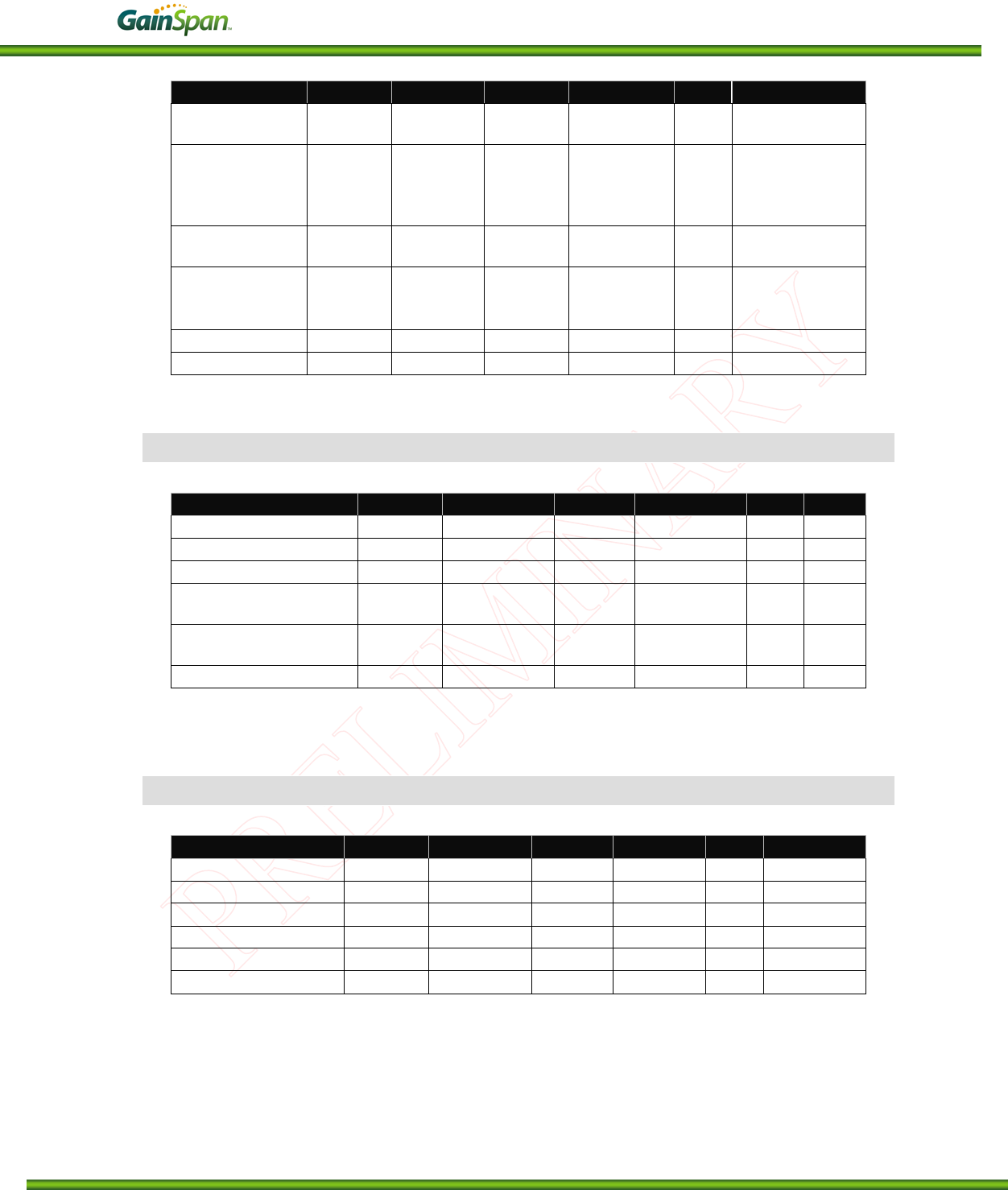
Table 4-1: Absolute Maximum Ratings
NOTE: For limitations on state voltage ranges, please consult section 2.6.1 Power supply.
4.2 Operating Conditions
Parameter
Symbol
Minimum
Typical
Maximum
Unit
Extended temp. range
T
A
-40
+85
ºC
RTC Power Supply
Vbat
2.5
3.3
3.6
V
I/O Supply voltage
VDDIO
1.7
3.3
3.6
V
Single Supply Port
GS1500M VIN_3V3 2.7 3.3 3.6 V
Table 4-2: Operating Conditions
4.3 Internal 1.8V regulator
VIN_3V3=VDDIO=Vbat=3.3V Temp=25ºC fOSC=3.0MHz
Parameter Symbol
Test
conditions Minimum Typical Maximum Unit
Output Voltage
VOUT_1V8
1.8
V
Maximum Output Current
IVOUT_1V8
30
50
mA
Oscillation Frequency fOSC 1.6 3.45 MHz
1.8V Regulator Enable
"H" Voltage EN_1V8
1.0 VIN_3V3 V
1.8V Regulator Enable
"L" Voltage EN_1V8
0 0.25 V
Table 4-3: Internal 1.8V Regulator

GS1500M DATA SHEET
PRELIMINARY GAINSPAN CONFIDENTIAL PAGE 25 OF 43
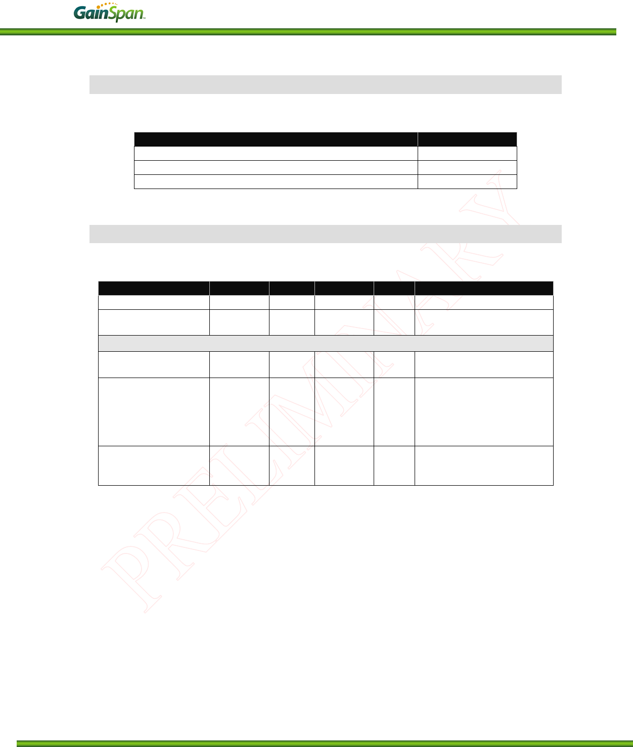
4.4 I/O DC Specifications
4.4.1 Digital Input Specifications
Parameter
Symbol
Minimum
Typical
Maximum
Unit
Note
Input Low Voltage
V
IL
-0.3
0.25* VDDIO
V
Input High Voltage V
IH
0.8*
VDDIO VDDIO V
Table 4-4: Digital Input Parameters
4.4.2 Digital Output Specification
Parameter
Symbol
Mininum
Typical
Maximum
Unit
Note
Output Low
Voltage V
OL
0 0.4 V With 4 mA load
Output High
Voltage V
OH
1.3 V
VDDIO V
V
DDIO
=3.0V, DC
current load 4.0 mA
V
DDIO
=1.62 V, DC
current
load 2.0 mA
Output rise
time @
VDDIO=3.3V t
TLH
7 ns
With 4 mA, 33 pF load
Output fall
time @
VDDIO=3.3V t
THL
7 ns
With 4 mA, 33 pF load
Table 4-5: Digital Output Parameters
4.4.3 I/O Digital Specifications (Tri-State)
Parameter
Symbol
Mininum
Typical
Maximum
Unit
Note
Input Low Voltage
V
IL
-0.3
0.25* VDDIO
V
Input High
Voltage V
IH
0.8*
VDDIO VDDIO V
Schmitt trig. Low
to High threshold
point V
T+
1.5 V
Schmitt trig. High
to Low threshold
point V
T-
1 V
Input Leakage
Current I
L
5
µ
A Pull up/down
disabled
Tri-State Output
Leakage Current Oz
L
5
µ
A
Pull up/down
disabled
Pull-Up Resistor R
u
0.05 1
M
Ω
Pull-Down
Resistor R
d
0.05 1
M
Ω
GS1500M DATA SHEET
PRELIMINARY GAINSPAN CONFIDENTIAL PAGE 26 OF 43
Parameter Symbol Mininum Typical Maximum Unit Note
Output Low
Voltage V
OL
0 0.4 V
With 4/12/20 mA
load
Output High
Voltage V
OH
1.3 V
VDDIO V
With 4/12/20 mA
load
With 2/6/10 mA
load
Output rise time
@ VDDIO =3.3V t
ToLH
7 ns With 4/12/20 mA
load, 33 pF
Output fall time @
VDDIO = 3.3V
t
ToHL
7
ns
With 4/12/20 mA
load, 33 pF
Input rise time
t
TiLH
7
ns
Input fall time
t
TiHL
7
ns
Table 4-6: I/O Digital Parameters
4.4.4 RTC Input Specifications (with Schmitt Trigger)
Parameter
Symbol
Mininum
Typical
Maximum
Unit
Note
I/O Supply Voltage
V
DDRTC
1.2
Vbat
V
Input Low Voltage
V
IL
-0.3
0.25*V
DDRTC
V
Input High Voltage V
IH
0.8*V
DDRTC
V
DDRTC
V
Schmitt trig. Low to High
threshold point V
T+
0.57*V
DDRTC
0.68*V
DDRTC
V
Schmitt trig. High to Low
threshold point V
T-
0.27*V
DDRTC
0.35*V
DDRTC
V
Input Leakage Current
I
L
260
pA
Table 4-7: RTC Input Parameters
4.4.5 RTC Output Specifications
Parameter
Symbol
Mininum
Typical
Maximum
Unit
Note
I/O Supply Voltage
V
DDRTC
1.2
Vbat
V
Output Low Voltage
V
OL
0
0.4
V
Output High Voltage
V
OH
0.8*V
DDRTC
V
DDRTC
V
Output rise time
t
TLH
19
142
ns
50 pF load
Output fall time
t
THL
21
195
ns
50 pF load
Input Leakage Current
I
L
730
pA
Table 4-8: RTC Output Parameters
GS1500M DATA SHEET
PRELIMINARY GAINSPAN CONFIDENTIAL PAGE 27 OF 43
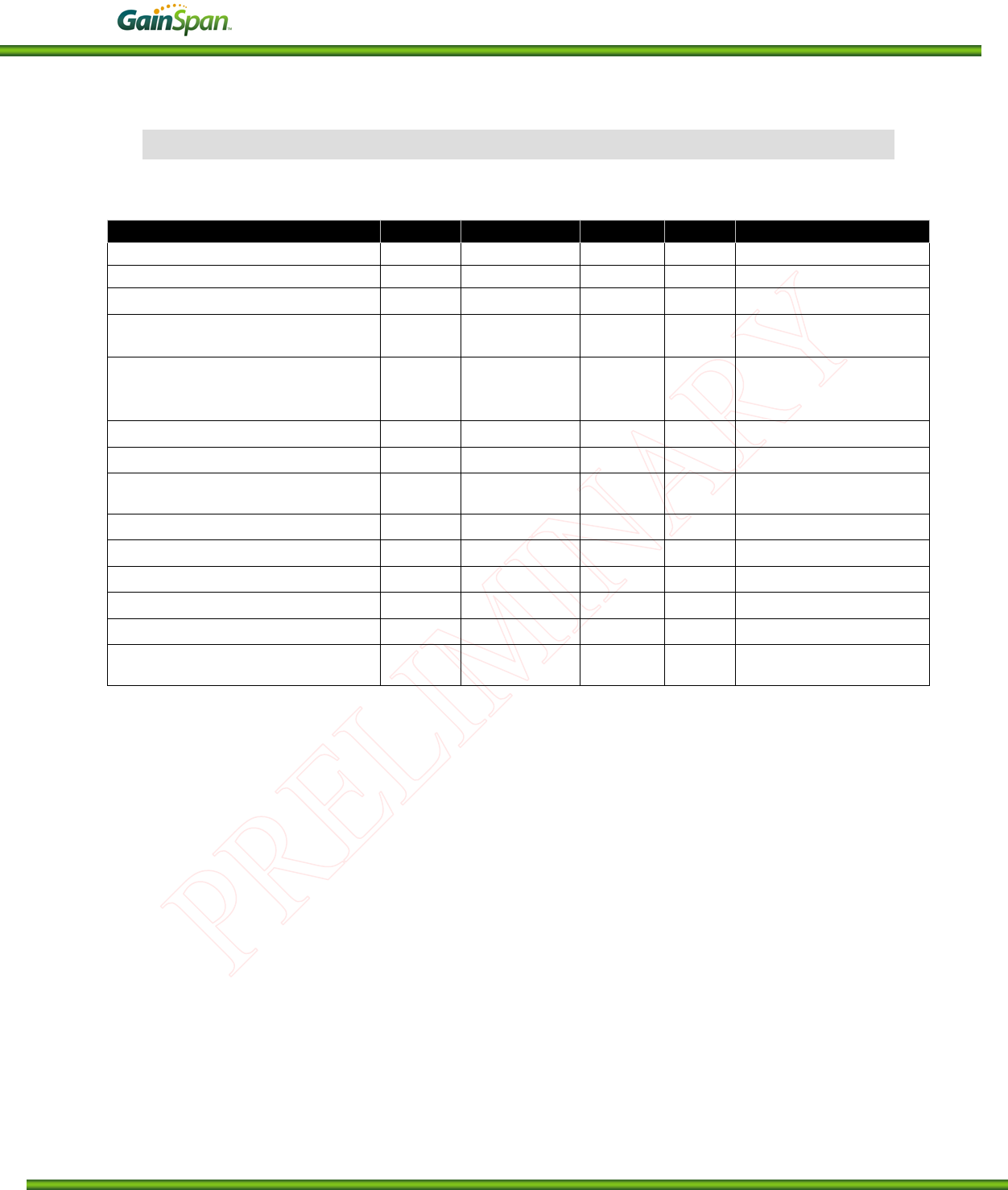
4.5 Power Consumption (estimated)
Test Conditions: VDD33=VDDIO=Vbat=3.3V Temp=25ºC
System state
Current (Typ.)
Deep Sleep
3mA
Receive (GS1500M; -xx dBm RX sens. @ xxMbps.
TBD
Transmit (GS1500M; xx dBm at antenna port @ 11n HT20 MCS7)
TBD
Table 4-9: Power Consumption in Different States
4.6 Radio Parameters
Test Conditions: VIN_3V3=VDDIO=Vbat=3.3V Temp=25ºC
Parameter Minimum Typical Maximum Unit Notes
RF Frequency range 2412 2497 MHz
Radio bit rate 1
HT20
MCS7 Mbps
Transmit/Recieve specification for GS1500M
Output power (average) 11 dBm
Modulated signal at antenna
port; 54 Mbps.
Spectrum Mask
F0 +/- 11 MHz
Offset >= 22 MHz
-TBD
-TBD
dBr Modulated signal at antenna
port
Receive Sensitivity at
antenna port
-TBD
-73
-94
dBm
HT20, MCS7 OFDM, 8% PER
54 Mbps OFDM, 8% PER
1 Mbps BPSK, 8% PER
Table 4-10: Radio Parameters
GS1500M DATA SHEET
PRELIMINARY GAINSPAN CONFIDENTIAL PAGE 28 OF 43
4.7 ADC Parameters
Test Conditions: VIN_3V3=VDDIO=Vbat=3.3V Temp=25ºC
Parameter
Minimum
Typical
Maximum
Unit
Notes
ADC Resolution
-
10
-
Bits
ADC Sample Freq
1.024
-
31.25
ksps
ADC input Clock Freq 32.768 - 1000 kHz
ADC Full Scale Voltage VOUT_1V8 –
0.036 V
Reference =
VOUT_1V8
Conversion Time 32 Clocks
Based on internally
generated 1MHz or
32.768 KHz Clocks
ADC Integral Non-Linearity (INL) -2.0 - 2.0 LSB
ADC Differential non-linearity (DNL) -1.0 - 1.0 LSB
AVDD Power Supply current
(operational) - 400 800
µ
A
ADC Offset Error -10 - 10 mV
ADC Gain Error -10 - 10 mV
Settling Time - 1
µ
S
Input resistance 1 - - MOhm
Input Capacitance - 10 - pF
Bandgap Output Voltage (Vref) (T = 25
ºC) 1.179 1.24 1.301 V
Table 4-11: ADC Parameters
GS1500M DATA SHEET
PRELIMINARY GAINSPAN CONFIDENTIAL PAGE 29 OF 43
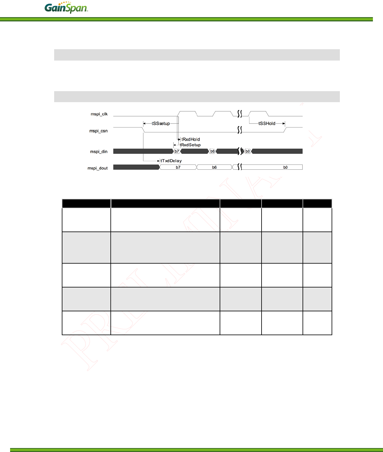
4.8 SPI Interface Timing
Test Conditions: VIN_3V3=VDDIO=Vbat=3.3V Temp=25ºC
4.8.1 Motorola SPI, clock polarity SPO = 0, clock phase SPH = 0
Figure 4-1: timing diagram, Master mode, SPO=SPH=0.
Parameter
Description
Minimum
Maximum
Unit
tSSetup
Minimum time between falling
edge of Select line and first rising
edge of SPI clock
1
MSPI
clock
period
tTxdDelay Delay in Master asserting TX line
after falling edge of Select line
2 core SPI
clock
periods +
3 nsec
mixed
tRxdSetup
Time before rising edge of SPI
clock by which received data must
be ready
30 nsec
tRxdHold
Time for which received data
must be stable after rising edge of
SPI clock
10 nsec
tSSHold
Time for which the Select line will
be held after the sampling edge
for the final bit to be transferred
1
MSPI
clock
period
Table 4-12: timing parameters, Master mode, SPO=SPH=0.
GS1500M DATA SHEET
PRELIMINARY GAINSPAN CONFIDENTIAL PAGE 30 OF 43
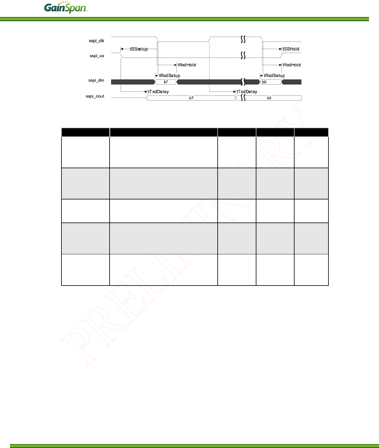
Figure 4-2: timing diagram, Slave mode, SPO=SPH=0.
Parameter
Description
Minimum
Maximum
Unit
tSSetup Minimum time between falling
edge of Select line and first rising
edge of SPI clock.
4 core SPI
clock
periods + 68
ns
mixed
tTxdDelay
Delay in Slave asserting TX line
after falling edge of SPI clock, or
the first bit after falling edge of the
Select line.
4 core
SPI clock
periods +
68 ns
mixed
tRxdSetup
Time before rising edge of SPI
clock by which received data must
be ready
15 ns
tRxdHold Time for which received data
must be stable after rising edge of
SPI clock
3 core SPI
clock
periods + 14
ns
mixed
tSSHold Time for which the Select line will
be held after the sampling edge
for the final bit to be transferred
3 core SPI
clock
periods + 14
ns
mixed
Table 4-13: timing parameters, Slave mode, SPO=SPH=0.
GS1500M DATA SHEET
PRELIMINARY GAINSPAN CONFIDENTIAL PAGE 31 OF 43
4.8.2 Motorola SPI, clock polarity SPO = 0, clock phase SPH = 1
Figure 4-3: timing diagram, Master, SPO=0, SPH=1.
Parameter
Description
Minimum
Maximum
Unit
tSSetup
Minimum time between falling
edge of select line and first rising
edge of SPI clock.
1.5
MSPI
clock
period
tTxdDelay
Delay in Master asserting TX line
after rising edge of SPI clock.
0 ns
tRxdSetup
Time before falling edge of SPI
clock by which received data must
be ready.
30 ns
tRxdHold
Time for which received data
must be stable after falling edge
of SPI clock.
10 ns
tSSHold
Time for which the Select line will
be held low after the sampling
edge for the final bit to be
transferred.
0.5 MSPI
clock
period
Table 4-14: timing parameters, Master mode; SPO=0, SPH=1.
GS1500M DATA SHEET
PRELIMINARY GAINSPAN CONFIDENTIAL PAGE 32 OF 43
Figure 4-4: timing diagram, Slave, SPO=0, SPH=1.
Parameter
Description
Minimum
Maximum
Unit
tSSetup
Minimum time between falling
edge of select line and first rising
edge of SPI clock.
15 ns
tTxdDelay Delay in Slave asserting TX line
after rising edge of SPI clock.
4 core SPI
clock
periods +
68 ns
mixed
tRxdSetup
Time before falling edge of SPI
clock by which received data must
be ready.
15 ns
tRxdHold Time for which received data
must be stable after falling edge
of SPI clock.
3 core SPI
clock
periods +
14 ns
mixed
tSSHold
Time for which the Select line will
be held low after the sampling
edge for the final bit to be
transferred.
3 core SPI
clock
periods +
14 ns
mixed
Table 4-15: timing parameters, Slave mode, SPO=0, SPH=1.
GS1500M DATA SHEET
PRELIMINARY GAINSPAN CONFIDENTIAL PAGE 33 OF 43
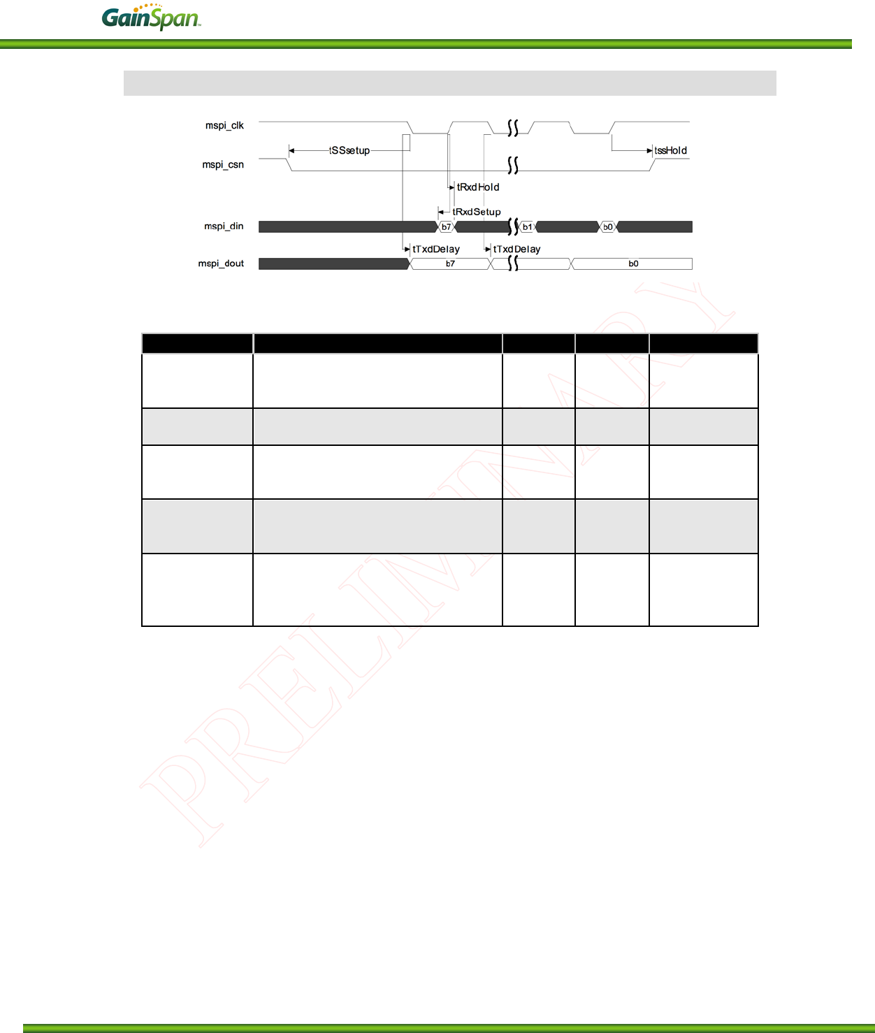
4.8.3 Motorola SPI, clock polarity SPO = 1, clock phase SPH = 0
Figure 4-5: timing diagram, Master mode, SPO=1, SPH=0.
Parameter
Description
Minimum
Maximum
Unit
tSSetup
Minimum time between falling
edge of select line and first falling
edge of SPI clock.
1
MSPI
clock
period
tTxdDelay Delay in Master asserting TX line
after falling edge of Select line.
2 core SPI
clock
periods +
3 ns
mixed
tRxdSetup
Time before falling edge of SPI
clock by which received data must
be ready.
30 ns
tRxdHold
Time for which received data
must be stable after falling edge
of SPI clock.
10 ns
tSSHold
Time for which the Select line will
be held low after the sampling
edge for the final bit to be
transferred.
1 MSPI
clock
period
Table 4-16: timing parameters, Master mode, SPO=1, SPH=0.
GS1500M DATA SHEET
PRELIMINARY GAINSPAN CONFIDENTIAL PAGE 34 OF 43
Figure 4-6: timing diagram, Slave mode, SPO=1, SPH=0.
Parameter Description Minimum Maximum Unit
tSSetup Minimum time between falling
edge of Select line and first falling
edge of SPI clock.
4 core SPI
clock
periods +
68 ns
Mixed
tTxdDelay
Delay in Slave asserting TX line
after rising edge of SPI clock, or
the first bit after falling edge of the
Select line.
4 core SPI
clock
periods +
68 ns
Mixed
tRxdSetup
Time before falling edge of SPI
clock by which received data must
be ready.
15 ns
tRxdHold Time for which received data
must be stable after falling edge
of SPI clock.
3 core SPI
clock
periods +
14 ns
Mixed
tSSHold
Time for which the Select line will
be held low after the sampling
edge for the final bit to be
transferred.
3 core SPI
clock
periods +
14 ns
MSPI
clock
period
Table 4-17: timing parameters, Slave mode, SPO=1, SPH=0.
GS1500M DATA SHEET
PRELIMINARY GAINSPAN CONFIDENTIAL PAGE 35 OF 43
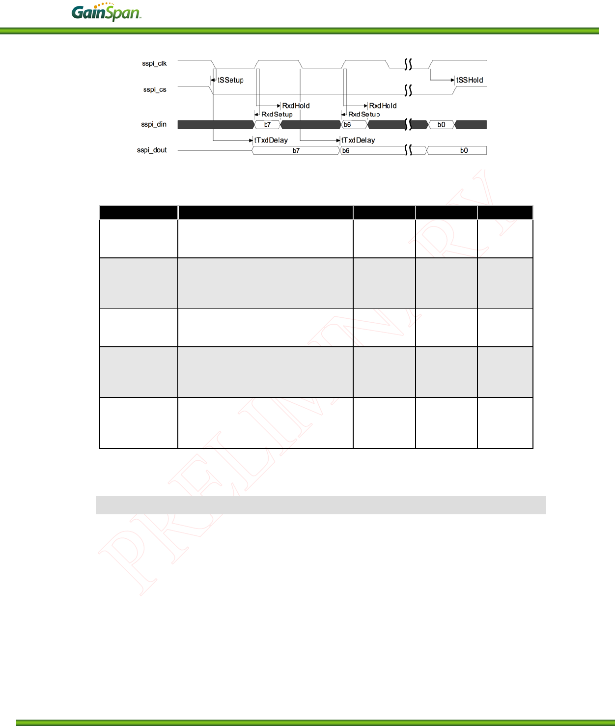
4.8.4 Motorola SPI, clock polarity SPO = 1, clock phase SPH = 1
Figure 4-7: timing diagram, Master mode, SPO=SPH=1.
Parameter
Description
Minimum
Maximum
Unit
tSSetup
Minimum time between falling
edge of select line and first falling
edge of SPI clock.
1.5 MSPI clock
period
tTxdDelay Delay in Master asserting TX line
after falling edge of SPI clock.
0 ns
tRxdSetup
Time before rising edge of SPI
clock by which received data must
be ready.
30 ns
tRxdHold
Time for which received data
must be stable after rising edge of
SPI clock.
10 ns
tSSHold
Time for which the Select line will
be held low after the sampling
edge for the final bit to be
transferred.
0.5 MSPI clock
period
Table 4-18: timing parameters, Master mode, SPO=SPH=1.
GS1500M DATA SHEET
PRELIMINARY GAINSPAN CONFIDENTIAL PAGE 36 OF 43
Figure 4-8: timing diagram, Slave mode, SPO=SPH=1.
Parameter
Description
Minimum
Maximum
Unit
tSSetup
Minimum time between falling
edge of select line and first falling
edge of SPI clock.
15 ns
tTxdDelay Delay in Slave asserting TX line
after falling edge of SPI clock.
4 core SPI
clock
periods +
68 ns
Mixed
tRxdSetup
Time before rising edge of SPI
clock by which received data must
be ready.
15 ns
tRxdHold Time for which received data
must be stable after rising edge of
SPI clock.
3 core SPI
clock
periods +
14 ns
Mixed
tSSHold
Time for which the Select line will
be held low after the sampling
edge for the final bit to be
transferred.
3 core SPI
clock
periods +
14 ns
Mixed
Table 4-19: timing parameters, Master mode, SPO=SPH=1.
4.9 Electrostatic discharge (ESD)
TBD
GS1500M DATA SHEET
PRELIMINARY GAINSPAN CONFIDENTIAL PAGE 37 OF 43
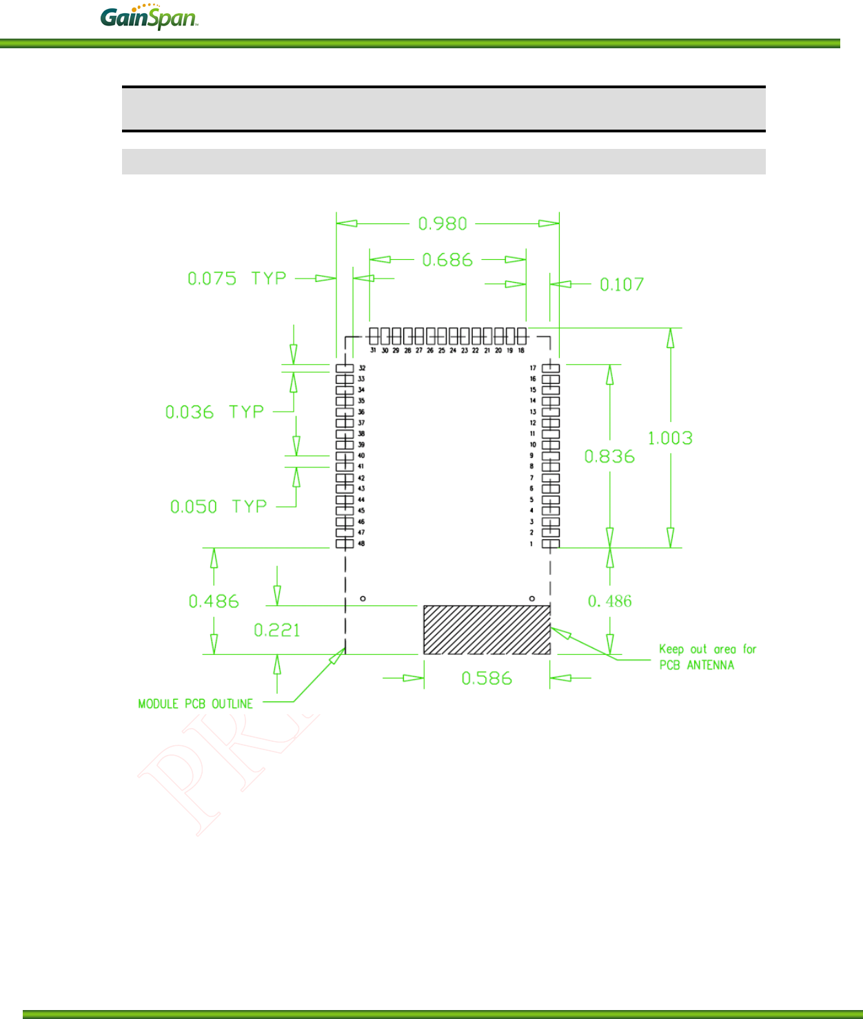
5 Package and Layout Guidelines
5.1 GS1500M Recommended PCB Footprint and Dimensions
Figure 5-1: GS1500M Module Recommended PCB Footprint (dimensions are in inches)
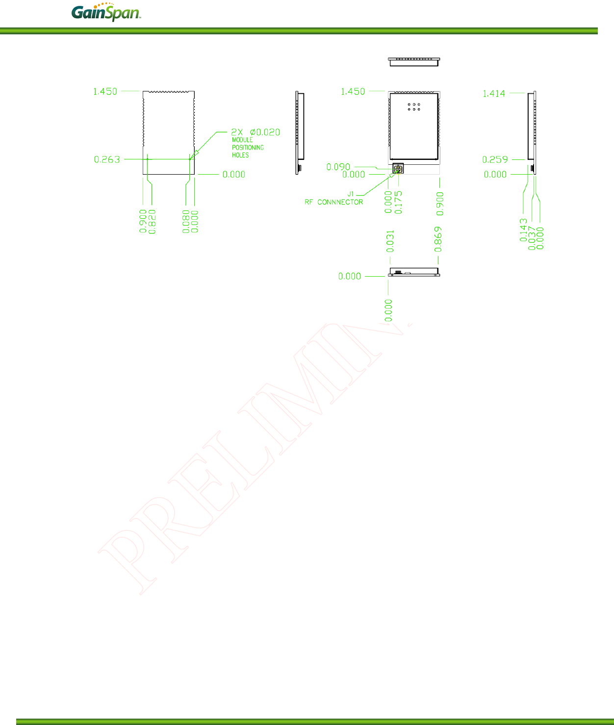
GS1500M DATA SHEET
PRELIMINARY GAINSPAN CONFIDENTIAL PAGE 38 OF 43
Figure 5-2: GS1500M Module Dimensions (in inches)
GS1500M DATA SHEET
PRELIMINARY GAINSPAN CONFIDENTIAL PAGE 39 OF 43
6 Ordering Information
DEVICE DESCRIPTION ORDERING NUMBER Rev
Low power module using PCB antenna
GS1500M
Rev X.X

GS1500M DATA SHEET
PRELIMINARY GAINSPAN CONFIDENTIAL PAGE 40 OF 43
7 Regulatory Notes
Federal Communication Commission Interference Statement
This equipment has been tested and found to comply with the limits for a Class B digital device, pursuant
to Part 15 of the FCC Rules. These limits are designed to provide reasonable protection against harmful
interference in a residential installation. This equipment generates uses and can radiate radio frequency
energy and, if not installed and used in accordance with the instructions, may cause harmful interference
to radio communications. However, there is no guarantee that interference will not occur in a particular
installation. If this equipment does cause harmful interference to radio or television reception, which can
be determined by turning the equipment off and on, the user is encouraged to try to correct the
interference by one of the following measures:
- Reorient or relocate the receiving antenna.
- Increase the separation between the equipment and receiver.
- Connect the equipment into an outlet on a circuit different from that to which the receiver is connected.
- Consult the dealer or an experienced radio/TV technician for help.
FCC Caution: To assure continued compliance, (example - use only shielded interface cables when
connecting to computer or peripheral devices). Any changes or modifications not
expressly approved by the party responsible for compliance could void the user's authority to
operate this equipment.
This device complies with Part 15 of the FCC Rules. Operation is subject to the following two
conditions: (1) This device may not cause harmful interference, and (2) this device must accept
any interference received, including interference that may cause undesired operation.
IMPORTANT NOTE:
FCC & IC Radiation Exposure Statement:
This equipment complies with FCC & IC radiation exposure limits set forth for an uncontrolled
environment. This equipment should be installed and operated with minimum distance 20cm between the
radiator & your body.
This transmitter must not be co-located or operating in conjunction with any other antenna or transmitter.
This device is intended only for OEM integrators under the following conditions:
1) The antenna must be installed such that 20 cm is maintained between the antenna and
users, and
2) The transmitter module may not be co-located with any other transmitter or antenna.
As long as 2 conditions above are met, further transmitter test will not be required. However, the
OEM integrator is still responsible for testing their end-product for any additional compliance
requirements required with this module installed (for example, digital device emissions, PC peripheral
requirements, etc.).
IMPORTANT NOTE: In the event that these conditions cannot be met (for example certain
laptop configurations or co-location with another transmitter), then the FCC & IC authorizations
are no longer considered valid and the FCC & IC IDs cannot be used on the final product. In
these circumstances, the OEM integrator will be responsible for re-evaluating the end product
(including the transmitter) and obtaining separate FCC & IC authorizations.
End Product Labeling
This transmitter module is authorized only for use in device where the antenna may be installed
such that 20 cm may be maintained between the antenna and users (for example access points, routers,
wireless ADSL modems, and similar equipment). The final end product must be labeled in a visible area
with the corresponding FCC ID number.

GS1500M DATA SHEET
PRELIMINARY GAINSPAN CONFIDENTIAL PAGE 41 OF 43
IC Certification — Canada
The labeling requirements for Industry Canada are similar to those of the FCC. A visible label on the
outside of the final product must display the IC labeling. The user is responsible for the end product to
comply with IC ICES-003 (Unintentional radiators)
Manual Information That Must be Included
The user’s manual for end users must include the following in-formation in a prominent location.
IMPORTANT NOTE: To comply with FCC & IC RF exposure compliance requirements, the
antenna used for this transmitter must be installed to provide a separation distance of at least 20 cm from
all persons and must not be co-located or operating in conjunction with any other antenna or transmitter.
Other notes:
GainSpan modules have been built or under development for near body exposure applications.
The 20cm statement is a standard note because absorption rate testing (commonly known as
SAR or Specific absorption rate) is not modularly transferable for FCC/IC. Thus, if a radio is
being used against the body, the end user is still responsible to test for regulatory near body
exposure testing (for USA, please refer to the following):
• FCC Part 1.1037
• FCC Part 2.1091 Mobile Devices
• FCC Part 2.1093 Portable Devices
• FCC Part 15.247 (b) (4)

GS1500M DATA SHEET
PRELIMINARY GAINSPAN CONFIDENTIAL PAGE 42 OF 43
8 Limitations
THIS DEVICE AND ASSOCIATED SOFTWARE ARE NOT DESIGNED, MANUFACTURED OR
INTENDED FOR USE OR RESALE FOR THE OPERATION OF APPLICATION IN A
HAZARDOUS ENVIRONMENT, OR REQUIRING FAIL-SAFE PERFORMANCE, OR IN WHICH
THE FAILURE OF PRODUCTS COULD LEAD DIRECTLY TO DEATH, PERSONAL INJURY, OR
SEVERE PHYSICAL OR ENVIRONMENTAL DAMAGE (COLLECTIVELY, "HIGH RISK
APPLICATIONS"). YOU AGREE AND ACKNOWLEDGE THAT YOU HAVE NO LICENSE TO,
AND SHALL NOT (AND SHALL NOT ALLOW A THIRD PARTY TO) USE THE TECHNOLOGY
IN ANY HIGH RISK APPLICATIONS, AND LICENSOR SPECIFICALLY DISCLAIMS ANY
WARRANTY REGARDING, AND ANY LIABILITY ARISING OUT OF, HIGH RISK
APPLICATIONS.
GS1500M DATA SHEET
PRELIMINARY GAINSPAN CONFIDENTIAL PAGE 43 OF 43
9 References
[
[1
1]
]
Title Wireless LAN Medium Access Control (MAC) and Physical Layer (PHY) Specifications
Reference IEEE Standard 802.11-2007
Version Date June 12, 2007
Source IEEE
[
[2
2]
]
Title GS1011 Peripheral and Register Description
Reference GS1011-PRD
Version 1.0 Date November 11, 2009
Source GainSpan
[
[3
3]
]
Title GS1011 ULTRA LOW-POWER WIRELESS SYSTEM-ON-CHIP DATA SHEET
Reference GS1011-DS
Version 1.0 Date November 9, 2009
Source GainSpan