GatesAir CZF Ranger CZ725F User Manual 2604s100
GatesAir, Inc. Ranger CZ725F 2604s100
UserManual.wiki
>
GatesAir
>
CZF User Manual
>
Users Manual E
Contents
1.
Users Manual D0
2.
Users Manual D1
3.
Users Manual D1A
4.
Users Manual D2
5.
Users Manual E
Users Manual E
Navigation menu
Upload a User Manual
Namespaces
Wiki Guide
HTML
PDF
Info
Views
User Manual
Discussion / Help
Navigation


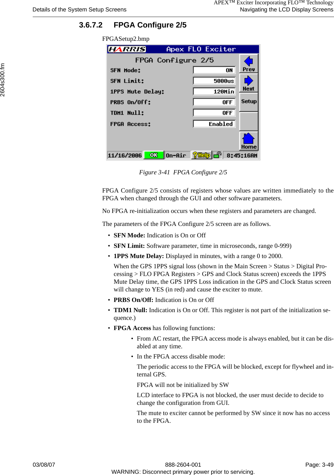
![APEX™ Exciter Incorporating FLO™ TechnologyNavigating the LCD Display Screens Details of the System Setup ScreensPage: 3-48 888-2604-001 03/08/07WARNING: Disconnect primary power prior to servicing.3.6.7 FPGA SetupThe FPGA modulator setup is accomplished in the following nine screens.3.6.7.1 FPGA Configure 1/5FPGASetup1.bmpFigure 3-40 FPGA Configure 1/5FPGA Configure 1/5 consists of registers whose values are written immediately to theFPGA when changed through the GUI. No FPGA re-initialization occurs when any of these registers are changed.The parameters of the FPGA Configure 1/5 screen are as follows.•Transmitter ID: (Unsigned 16-bit Decimal, range 0 to 65535)•Wide Area PID: (Unsigned 13-bit Decimal, range 0 to 8191)•Local Area PID: (Unsigned 13-bit Decimal, range 0 to 8191)•TS Stream Control: (TS1 Active/TS2 Active)•TS Source Control: (Automatic/Manual)•Infrastructure ID: (Unsigned 16-bit Decimal, range 0 to 65535)•Local Time Offset: (Signed Real Decimal in Hours, range -16.0 to +15.5 in 0.5 in-crements Register value is calculated as [Local Time Offset]*2)•Daylight Savings: (Standard/Daylight)](https://usermanual.wiki/GatesAir/CZF.Users-Manual-E/User-Guide-939483-Page-88.png)