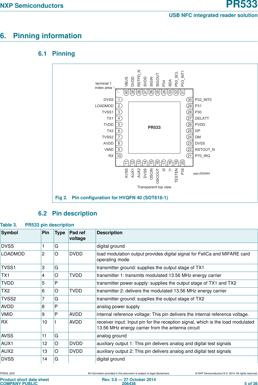
Getac Technology PR533A RFID module User Manual PR533 USB NFC integrated reader solution
Getac Technology Corporation RFID module PR533 USB NFC integrated reader solution
UserManual.wiki
>
Getac Technology
>
PR533A User Manual
>
User Manual Module
Contents
1.
User Manual Host
2.
User Manual Module
User Manual Module
Navigation menu
Upload a User Manual
Namespaces
Wiki Guide
HTML
PDF
Info
Views
User Manual
Discussion / Help
Navigation
![PR533_SDS All information provided in this document is subject to legal disclaimers. © NXP Semiconductors N.V. 2014. All rights reserved.Product short data sheetCOMPANY PUBLICRev. 3.6 — 27 October 2014206436 3 of 36NXP Semiconductors PR533USB NFC integrated reader solutionDedicated I/O ports for external device control3. Quick reference data [1] VDDD, VDDA and VDD(TVDD) must always be at the same supply voltage.Table 1. Quick reference dataSymbol Parameter Conditions Min Typ Max UnitVBUS bus supply voltage 4.02 5 5.25 V(non-USB mode); VBUS =VDDD; VSSD =0V2.5 3.3 3.6 VVDDA analog supply voltage VDDA = VDDD = VDD(TVDD) = VDD(PVDD); VSSA = VSSD = VSS(PVSS) = VSS(TVSS) = 0 V[1] 2.5 3.3 3.6 VVDDD digital supply voltage [1] 2.5 3.3 3.6 VVDD(TVDD) TVDD supply voltage [1] 2.5 3.3 3.6 VVDD(PVDD) PVDD supply voltage 1.6 - 3.6 VVDD(SVDD) SVDD supply voltage VSSA = VSSD = VSS(PVSS) = VSS(TVSS) = 0 V; reserved for future useVDDD 0.1 - VDDD VIBUS bus supply current maximum load current (USB mode); measured on VBUS150 mAmaximum inrush current lim-itation; at power-up (curlimoff = 0)100 mAIpd power-down current VDDA = VDDD = VDD(TVDD) = VDD(PVDD) = 3 V; not powered from USBhard power-down; RF level detector off10 Asoft power-down; RF level detector on30 AICCSL suspended low-power device supply currentRF level detector on, (with-out resistor on DP/DM)--250AIDDD digital supply current RF level detector on, VDD(SVDD) switch off[1] -15-mAIDD(SVDD) SVDD supply current VDDS = 3 V - - 30 mAIDDA analog supply current RF level detector on - 6 - mAIDD(TVDD) TVDD supply current during RF transmission; VDD(TVDD) =3 V-60100mAPtot total power dissipation Tamb =30 to +85 C--0.55WTamb ambient temperature 30 - +85 C](https://usermanual.wiki/Getac-Technology/PR533A.User-Manual-Module/User-Guide-3466028-Page-3.png)
![PR533_SDS All information provided in this document is subject to legal disclaimers. © NXP Semiconductors N.V. 2014. All rights reserved.Product short data sheetCOMPANY PUBLICRev. 3.6 — 27 October 2014206436 4 of 36NXP Semiconductors PR533USB NFC integrated reader solution4. Ordering information [1] 60 or 70 refers to the ROM code version described in the User Manual. For differences of romcode versions refer to the release note of the product.[2] Refer to Section 14.4 “Licenses”.[3] MSL 2 (Moisture Sensitivity Level).5. Block diagramThe following block diagram describes hardware blocks controlled by PR5331C3HN firmware or which can be accessible for data transaction by a host baseband. Table 2. Ordering informationType number Package Name Description VersionPR5331C3HN/C360[1][2][3] HVQFN40 plastic thermal enhanced very thin quad flat package; no leads; 40 terminals; body 6 6 0.85 mmSOT618-1PR5331C3HN/C370[1][2][3]Fig 1. Block diagramaaa-000043SUPPLYSUPERVISOR27 MHz OSCANDFRAC NPLLSVDDSWITCHNFCANALOGFRONT ENDANDCLUART80C51 CPU44 k ROM1.2 k BYTES RAMUSBDEVICEI2CMASTERMATXRSTPD_NPVDDSVDDVBUSP30 P31 P32_INT0GPIOsP33_INT0 P35RSTOUT_N DVDD P70_IRQ AVSSDVSSOSCINOSCOUTI0I1SDAP50_SCLDELATT48 MHzSIGINSIGOUTP34TVDDAVDDRXVMIDTX1TVSSTX2REGULATOR3.3 VPCR](https://usermanual.wiki/Getac-Technology/PR533A.User-Manual-Module/User-Guide-3466028-Page-4.png)
![PR533_SDS All information provided in this document is subject to legal disclaimers. © NXP Semiconductors N.V. 2014. All rights reserved.Product short data sheetCOMPANY PUBLICRev. 3.6 — 27 October 2014206436 7 of 36NXP Semiconductors PR533USB NFC integrated reader solution[1] Pin types: I= Input, O = Output, I/O = Input/Output, P = Power and G = Ground.7. Limiting values [1] 1500 , 100 pF; EIA/JESD22-A114-A[2] 0.75 mH, 200 pF; EIA/JESD22-A115-A[3] Field induced model; EIA/JESC22-C101-CRSTPD_N 38 I PVDD reset and power-down: When LOW, internal current sources are switched off, the oscillator is inhibited, and the input pads are disconnected from the out-side world. With a negative edge on this pin the internal reset phase starts.DVDD 39 P digital power supplyVBUS 40 P USB power supply.Table 3. PR533 pin description …continuedSymbol Pin Type Pad ref voltageDescriptionTable 4. Limiting valuesIn accordance with the Absolute Maximum Rating System (IEC 60134).Symbol Parameter Conditions Min Max UnitVDDA analog supply voltage 0.5 +4 VVDDD digital supply voltage 0.5 +4 VVDD(TVDD) TVDD supply voltage 0.5 +4 VVDD(PVDD) PVDD supply voltage 0.5 +4 VVDD(SVDD) SVDD supply voltage 0.5 +4 VVBUS bus supply voltage 0.5 +5.5 VPtot total power dissipation - 500 mWIDD(SVDD) SVDD supply current maximum current in VDDS switch-30 mAViinput voltage TX1, TX2, RX pins 0.5 +4 VVESD electrostatic discharge voltage HBM [1] 2.0 kVMM [2] -200VCDM [3] -1kVTstg storage temperature 55 +150 CTjjunction temperature 40 +125 CVi(dyn)(RX) dynamic input voltage on pin RX input signal at 13.56 MHz 0.7 VDD(AVDD) +1.0 VVi(dyn)(TX1) dynamic input voltage on pin TX1 input signal at 13.56 MHz 1.2 VDD(TVDD) +1.3 VVi(dyn)(TX2) dynamic input voltage on pin TX2 input signal at 13.56 MHz 1.2 VDD(TVDD) +1.3 VITX1 current on pin TX1 output signal at 13.56 MHz 300 +300 mAITX2 current on pin TX2 output signal at 13.56 MHz 300 +300 mA](https://usermanual.wiki/Getac-Technology/PR533A.User-Manual-Module/User-Guide-3466028-Page-7.png)
![PR533_SDS All information provided in this document is subject to legal disclaimers. © NXP Semiconductors N.V. 2014. All rights reserved.Product short data sheetCOMPANY PUBLICRev. 3.6 — 27 October 2014206436 8 of 36NXP Semiconductors PR533USB NFC integrated reader solution8. Recommended operating conditions [1] VSSA, VDDD and VDD(TVDD) shall always be on the same voltage level.[2] Supply voltages below 3 V reduces the performance (e.g. the achievable operating distance).9. Thermal characteristics 10. CharacteristicsUnless otherwise specified, the limits are given for the full operating conditions. The typical value is given for 25 C, VDDD = 3.4 V and VDD(PVDD) = 3 V in non-USB bus power mode, VBUS = 5 V in USB power mode.Timings are only given from characterization results.10.1 Power management characteristics10.1.1 Current consumption characteristicsTypical value using a complementary driver configuration and an antenna matched to 40 between TX1 and TX2 at 13.56 MHz.Table 5. Operating conditionsSymbol Parameter Conditions Min Typ Max UnitVBUS bus supply voltage VSSA = VSSD = VSS(PVSS) = VSS(TVSS) = 0 V 4.02 5 5.25 Vsupply voltage (non-USB mode); VBUS = VDDD; VSSA = VSSD = VSS(PVSS) = VSS(TVSS) = 0 V2.53.3 3.6VVDDA analog supply volt-ageVDDA = VDDD = VDD(TVDD) = VDD(PVDD); VSSA =VSSD = VSS(PVSS) = VSS(TVSS) = 0 V[1][2] 2.53.3 3.6VVDDD digital supply volt-ageVDDA = VDDD = VDD(TVDD) = VDD(PVDD); VSSA =VSSD = VSS(PVSS) = VSS(TVSS) = 0 V[1][2] 2.53.3 3.6VVDD(TVDD) TVDD supply volt-ageVDDA = VDDD = VDD(TVDD) = VDD(PVDD); VSSA =VSSD = VSS(PVSS) = VSS(TVSS) = 0 V[1][2] 2.53.3 3.6VVDD(PVDD) PVDD supply volt-agesupply pad for host interface; VDDA =VDDD =VDD(TVDD) = VDD(PVDD); VSSA =VSSD = VSS(PVSS) = VSS(TVSS) = 0 V[2] 1.6 1.8 to 3.3 3.6 VTamb ambient tempera-ture30 +25 +85 CTable 6. Thermal characteristicsSymbol Parameter Conditions Min Typ Max UnitRth(j-a) thermal resistance from junction to ambientin free air with exposed pad soldered on a 4 layer Jedec PCB-0.5-3741.1K/W](https://usermanual.wiki/Getac-Technology/PR533A.User-Manual-Module/User-Guide-3466028-Page-8.png)
![PR533_SDS All information provided in this document is subject to legal disclaimers. © NXP Semiconductors N.V. 2014. All rights reserved.Product short data sheetCOMPANY PUBLICRev. 3.6 — 27 October 2014206436 9 of 36NXP Semiconductors PR533USB NFC integrated reader solution [1] Ipd is the total currents over all supplies.[2] IDD(PVDD) depends on the overall load at the digital pins.[3] IDD(SVDD) depends on the overall load on VDD(SVDD) pad.[4] IDD(TVDD) depends on VDD(TVDD) and the external circuitry connected to TX1 and TX2.[5] During operation with a typical circuitry the overall current is below 100 mA.10.1.2 Voltage regulator characteristics [1] The internal regulator is only enabled when the USB interface is selected by I0 and I1.10.2 Antenna presence self test thresholdsThe values in Ta ble 9 are guaranteed by design. Only functional is done in production for cases andet_ithl[1:0] = 10b and for andet_ithh[2:0] = 011b.Table 7. Current consumption characteristicsSymbol Parameter Conditions Min Typ Max UnitIpd power-down current VDDA = VDDD = VDD(TVDD) = VDD(PVDD) = 3 V; not powered from USBhard power-down current; not powered from USB; RF level detector off[1] -1.310Asoft power-down current; not powered from USB; RF level detector on[1] -930AICCSL suspended low-power device supply currentVBUS =5V; VDDA = VDDD = VDD(TVDD) = VDD(PVDD) =3V; VDDS = 0 V; RF level detector on (without resistor on pin DP (D+))[1] - 120 250 AIDDD digital supply current VDDA = VDDD = VDD(TVDD) = VDD(PVDD) = 3 V; RF level detector on -12- mAIDDA analog supply current VDDA = VDDD = VDD(TVDD) = VDD(PVDD) =3V RF level detector on - 3 6 mARF level detector off - 1.5 5 mAIDD(PVDD) PVDD supply current [2] --30mAIDD(SVDD) SVDD supply current sam_switch_en set to 1 [3] --30mAIDD(TVDD) TVDD supply current continuous wave; VDD(TVDD) =3V [4][5] - 60 100 mATable 8. Voltage regulator characteristics[1]Symbol Parameter Conditions Min Typ Max UnitVBUS bus supply voltage USB mode; VSS = 0 V 4.02 5 5.25 VVDDD digital supply voltage after inrush current limitation (USB mode); from IVDDD = 0 mA to IVDDD =150mA2.95 3.3 3.6 VIBUS bus supply current USB mode; measure on VBUS --150mAIinrush(lim) inrush current limit at power-up (curlimofff = 0) - - 100 mAVth(rst)reg regulator reset threshold voltage regulator reset 1.90 2.15 2.40 VVth(rst)reg(hys) regulator reset threshold voltage hysteresis35 60 85 mVVDDD decoupling capacitor 8 10 - F](https://usermanual.wiki/Getac-Technology/PR533A.User-Manual-Module/User-Guide-3466028-Page-9.png)
![PR533_SDS All information provided in this document is subject to legal disclaimers. © NXP Semiconductors N.V. 2014. All rights reserved.Product short data sheetCOMPANY PUBLICRev. 3.6 — 27 October 2014206436 10 of 36NXP Semiconductors PR533USB NFC integrated reader solution Table 9. Antenna presence detectionParameter Conditions Min Typ Max UnitIVDDD lower current threshold for antenna presence detectionandet_ithl[1:0] 00b - 5 - mA01b - 15 - mA10b - 25 - mA11b - 35 - mAIVDDD upper current threshold for antenna presence detectionandet_ithh[2:0] 000b - 45 - mA001b - 60 - mA010b - 75 - mA011b - 90 - mA100b - 105 - mA101b - 120 - mA110b - 135 - mA111b - 150 - mA](https://usermanual.wiki/Getac-Technology/PR533A.User-Manual-Module/User-Guide-3466028-Page-10.png)
![PR533_SDS All information provided in this document is subject to legal disclaimers. © NXP Semiconductors N.V. 2014. All rights reserved.Product short data sheetCOMPANY PUBLICRev. 3.6 — 27 October 2014206436 11 of 36NXP Semiconductors PR533USB NFC integrated reader solution10.3 Typical 27.12 MHz Crystal requirements 10.4 Pin characteristics for 27.12 MHz XTAL Oscillator (OSCIN, OSCOUT) [1] n(th) and fn(th) define the mask for maximum acceptable phase noise of the clock signal at the OSCIN, OSCOUT inputs. See Figure 3 “27.12 MHz input clock phase noise spectrum mask”. Table 10. Crystal requirementsSymbol Parameter Conditions Min Typ Max Unitfxtal crystal frequency 27.107 27.12 27.133 MHzESR equivalent series resistance - - 100 CLload capacitance - 10 - pFPxtal crystal power dissipation 100 - - WTable 11. Pin characteristics for 27.12 MHz XTAL Oscillator (OSCIN, OSCOUT)Symbol Parameter Conditions Min Typ Max UnitILI input leakage current RSTPD_N = 0 V 1-+1mAVIH HIGH-level input voltage 0.7 VDDA -VDDA VVIL LOW-level input voltage 0 - 0.3 VDDA VVOH HIGH-level output voltage - 1.1 - VVOL LOW-level output voltage - 0.2 - Vfclk clock frequency 0.05 % 27.12 +0.05 % MHzduty cycle 40 50 60 %n(th) phase noise threshold [1] --140 dBc/Hzfn(th) phase noise threshold fre-quency n(th) = 140dBc/Hz; 20dB/decade slope[1] - - 50 kHzOSCINViinput voltage DC - 0.65 - VCiinput capacitance VDDA = 2.8 V; Vi(DC) = 0.65 V; Vi(AC) = 1 V p-p-2-pFOSCOUTCiinput capacitance - 2 - pFFig 3. 27.12 MHz input clock phase noise spectrum maskφn(th)phase noise(dBc/Hz)-20 dB/decade acceptable phase noise area001aao393fφn(th) frequency (Hz)](https://usermanual.wiki/Getac-Technology/PR533A.User-Manual-Module/User-Guide-3466028-Page-11.png)
![PR533_SDS All information provided in this document is subject to legal disclaimers. © NXP Semiconductors N.V. 2014. All rights reserved.Product short data sheetCOMPANY PUBLICRev. 3.6 — 27 October 2014206436 12 of 36NXP Semiconductors PR533USB NFC integrated reader solution10.5 RSTPD_N input pin characteristics 10.6 Input pin characteristics for I0, I1 and TESTEN [1] To minimize power consumption when in soft power-down mode, the limit is VDDD 0.4 V.[2] To minimize power consumption when in soft power-down mode, the limit is 0.4 V.[3] TESTEN should never be set to high level in the application. It is used for production test purpose only. It is recommended to connect TESTEN to ground although there is a pull-down included.Table 12. RSTPD_N input pin characteristicsSymbol Parameter Conditions Min Typ Max UnitVIH HIGH-level input volt-ageVDD(PVDD) 0.4 - VDD(PVDD) VVIL LOW-level input volt-age0-0.4VIIH HIGH-level input cur-rentVI=VDD(PVDD) 1-1AIIL LOW-level input current VI = 0 V 1-1ACiinput capacitance - 2.5 - pFTable 13. Input pin characteristics for I0, I1 and TESTENSymbol Parameter Conditions Min Typ Max UnitVIH HIGH-level input voltage [1] 0.7 VDDD -VDDD VVIL LOW-level input voltage [2] 00.3VDDD VIIH HIGH-level input current I0 and I1; VI=VDDD[3] 1-1 AIIL LOW-level input current VI=0V 1-1 ACiinput capacitance - 2.5 - pF](https://usermanual.wiki/Getac-Technology/PR533A.User-Manual-Module/User-Guide-3466028-Page-12.png)
![PR533_SDS All information provided in this document is subject to legal disclaimers. © NXP Semiconductors N.V. 2014. All rights reserved.Product short data sheetCOMPANY PUBLICRev. 3.6 — 27 October 2014206436 13 of 36NXP Semiconductors PR533USB NFC integrated reader solution10.7 RSTOUT_N output pin characteristics [1] Data at VDD(PVDD) = 1.8V are only given from characterization results.[2] IOH and IOL give the output drive capability from which the rise and fall times may be calculated as a function of the load capacitance.Table 14. RSTOUT_N output pin characteristicsSymbol Parameter Conditions Min Typ Max UnitVOH HIGH-level output voltageVDD(PVDD) =3V; IOH =4mA 0.7VDD(PVDD) -VDD(PVDD) VVDD(PVDD) =1.8V; IOH = 2mA [1] 0.7 VDD(PVDD) -VDD(PVDD) VVOL LOW-level output voltageVDD(PVDD) =3V; IOL =4mA 0 - 0.3VDD(PVDD) VVDD(PVDD) =1.8V; IOL =2mA [1] 0-0.3VDD(PVDD) VIOH HIGH-level output currentVDD(PVDD) =3V; VOH = 0.8 VDD(PVDD)[2] 4-- mAVDD(PVDD) =1.8V; VOH = 0.7 VDD(PVDD)2-- mAIOL LOW-level output currentVDD(PVDD) =3V; VOL = 0.2 VDD(PVDD)[2] 4--mAVDD(PVDD) =1.8V; VOL = 0.3 VDD(PVDD)2--mACLload capacitance - 30 pFtrrise time VDD(PVDD) =3V; VOH =0.8VDD(PVDD); CL =30pF--13.5nsVDDP =1.8V; VOH =0.7VDD(PVDD); CL=30pF--10.8nstffall time VDD(PVDD) =3V; VOL =0.2VDD(PVDD); CL =30pF--13.5nsVDD(PVDD) =1.8V; VOL =0.3VDD(PVDD); CL=30pF--10.8ns](https://usermanual.wiki/Getac-Technology/PR533A.User-Manual-Module/User-Guide-3466028-Page-13.png)
![PR533_SDS All information provided in this document is subject to legal disclaimers. © NXP Semiconductors N.V. 2014. All rights reserved.Product short data sheetCOMPANY PUBLICRev. 3.6 — 27 October 2014206436 14 of 36NXP Semiconductors PR533USB NFC integrated reader solution10.8 Input/output characteristics for pin P70_IRQ [1] To minimize power consumption when in soft power-down mode, the limit is VDD(PVDD) 0.4 V.[2] To minimize power consumption when in soft power-down mode, the limit is 0.4 V.[3] Data at VDD(PVDD) = 1.8 V are only given from characterization results.[4] The IOH and IOL give the output driving capability and allow to calculate directly the rise and fall time as function of the load capacitance.Table 15. Input/output pin characteristics for pin P70_IRQSymbol Parameter Conditions Min Typ Max UnitVIH HIGH-level input volt-age[1] 0.7 VDD(PVDD) -VDD(PVDD) VVIL LOW-level input voltage [2] 0-0.3VDD(PVDD) VVOH HIGH-level output volt-agepush-pull mode; VDD(PVDD) =3V; IOH =4mA0.7 VDD(PVDD) -VDD(PVDD) Vpush-pull mode; VDD(PVDD) = 1.8 V; IOH =-2mA[3] 0.7 VDD(PVDD) -VDD(PVDD) VVOL LOW-level output volt-agepush-pull mode; VDD(PVDD) =3V; IOL =4mA0-0.3VDD(PVDD) Vpush-pull mode; VDD(PVDD) = 1.8 V; IOL =2mA[3] 0-0.3VDD(PVDD) VIIH HIGH-level input current input mode; VI=VDDD 1-1 AIIL LOW-level input current input mode; VI=0V 1-1 AIOH HIGH-level output cur-rentVDD(PVDD) =3V; VOH =0.8VDD(PVDD)[5] 4-- mAIOL LOW-level output cur-rentVDD(PVDD) =3V; VOL =0.2VDD(PVDD)[5] 4--mAILI input leakage current RSTPD_N = 0.4 V 1-1 ACiinput capacitance - 2.5 pFCLload capacitance - - 30 pFtrrise time VDD(PVDD) =3V; VOH =0.8VDD(PVDD); CL=30pF--13.5nsVDD(PVDD) =1.8V; VOH =0.7VDD(PVDD); CL=30pF--10.8nstffall time VDD(PVDD) =3V; VOL =0.2VDD(PVDD); CL=30pF--13.5nsVDD(PVDD) =1.8V; VOL =0.3VDD(PVDD); CL=30pF--10.8ns](https://usermanual.wiki/Getac-Technology/PR533A.User-Manual-Module/User-Guide-3466028-Page-14.png)
![PR533_SDS All information provided in this document is subject to legal disclaimers. © NXP Semiconductors N.V. 2014. All rights reserved.Product short data sheetCOMPANY PUBLICRev. 3.6 — 27 October 2014206436 15 of 36NXP Semiconductors PR533USB NFC integrated reader solution10.9 Input/output pin characteristics for P30 / UART_RX, P31 / UART_TX, P32_INT0, P33_INT1 [1] To minimize power consumption when in soft power-down mode, the limit is VDD(PVDD) 0.4 V.[2] To minimize power consumption when in soft power-down mode, the limit is 0.4 V[3] Data at VDD(PVDD) = 1.8 V are only given from characterization results.[4] The IOH and IOL give the output driving capability and allow to calculate directly the rise and fall time as function of the load capacitance.Table 16. Input/output pin characteristics for P30 / UART_RX, P31 / UART_TX, P32_INT0, P33_INT1Symbol Parameter Conditions Min Typ Max UnitVIH HIGH-level input voltage [1] 0.7 VDD(PVDD) -VDD(PVDD) VVIL LOW-level input voltage [2] 0-0.3VDD(PVDD) VVOH HIGH-level output volt-agepush-pull mode; VDD(PVDD) =3V; IOH =4mAVDD(PVDD) 0.4 - VDD(PVDD) VVDD(PVDD) =1.8V; IOH =2mA[3] VDD(PVDD) 0.4 - VDD(PVDD) VVOL LOW-level output volt-agepush-pull mode; VDD(PVDD) =3V; IOL =4mA0-0.4VVDD(PVDD) =1.8V; IOL =2mA[3] 0-0.4VIIH HIGH-level input current input mode; VI=VDD(PVDD)1-1 AIIL LOW-level input current input mode; VI=0V 1-1 AIOH HIGH-level output cur-rentVDD(PVDD) =3V; VOH =0.8VDD(PVDD)[4] 4-- mAIOL LOW-level output current VDD(PVDD) =3V; VOL =0.2VDD(PVDD)[4] 4--mAILI input leakage current RSTPD_N = 0.4 V 1-1 ACiinput capacitance - 2.5 - pFCLload capacitance - - 30 pFtrrise time VDD(PVDD) =3V; VOH =0.8VDD(PVDD); CL=30pF--13.5nsVDD(PVDD) =1.8V; VOH =0.7VDD(PVDD); CL=30pF--10.8nstffall time VDD(PVDD) =3V; VOL =0.2VDD(PVDD); CL=30pF--13.5nsVDD(PVDD) =1.8V; VOL =0.3VDD(PVDD); CL=30pF--10.8ns](https://usermanual.wiki/Getac-Technology/PR533A.User-Manual-Module/User-Guide-3466028-Page-15.png)
![PR533_SDS All information provided in this document is subject to legal disclaimers. © NXP Semiconductors N.V. 2014. All rights reserved.Product short data sheetCOMPANY PUBLICRev. 3.6 — 27 October 2014206436 16 of 36NXP Semiconductors PR533USB NFC integrated reader solution10.10 Input/output pin characteristics for P35 [1] To minimize power consumption when in soft power-down mode, the limit is VDDD 0.4 V.[2] To minimize power consumption when in soft power-down mode, the limit is 0.4 V.[3] The IOH and IOL give the output driving capability and allow to calculate directly the rise and fall time as function of the load capacitance.Table 17. Input/output pin characteristics for P35Symbol Parameter Conditions Min Typ Max UnitVIH HIGH-level input voltage [1] 0.7 VDDD -VDDD VVIL LOW-level input voltage [2] 0-0.3VDDD VVOH HIGH-level output volt-ageVDDD =3V; IOH =4mA VDDD 0.4 - VDDD VVOL LOW-level output voltage VDDD =3V; IOL =4mA 0 - 0.4 VIIH HIGH-level input current VI=VDDD 1-1 AIIL LOW-level input current VI=0V 1-1 AIOH HIGH-level output current VDDD =3V; VOH =0.8VDD(PVDD)[3] 4-- mAIOL LOW-level output current VDDD =3V; VOL =0.2VDD(PVDD)[3] 4-- mAILI input leakage current RSTPD_N = 0.4 V 1-1 ACiinput capacitance - 2.5 - pFCLload capacitance - - 30 pFtrrise time VDDD =3V; VOH =0.8VDDD; CL=30pF--13.5nsVDDD =1.8V; VOH =0.7VDDD; CL=30pF--10.8nstffall time VDDD =3V; VOL =0.2VDDD; CL=30pF--13.5nsVDDD =1.8V; VOL =0.3VDDD; CL=30pF--10.8ns](https://usermanual.wiki/Getac-Technology/PR533A.User-Manual-Module/User-Guide-3466028-Page-16.png)
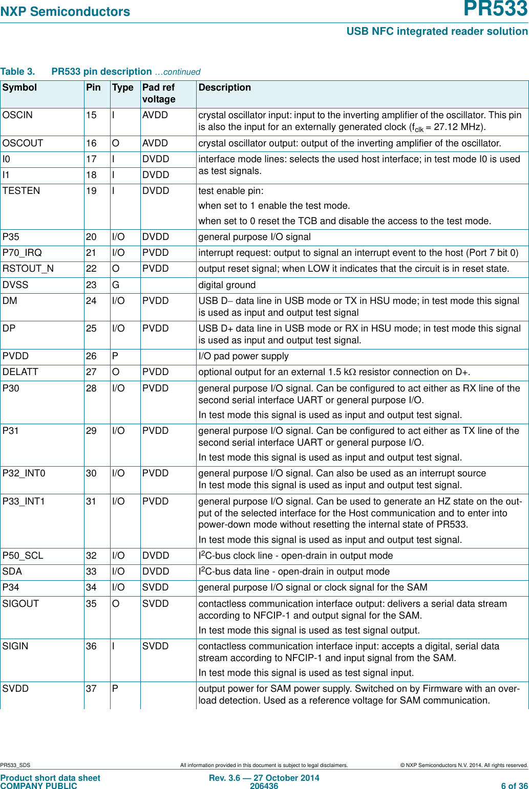
![PR533_SDS All information provided in this document is subject to legal disclaimers. © NXP Semiconductors N.V. 2014. All rights reserved.Product short data sheetCOMPANY PUBLICRev. 3.6 — 27 October 2014206436 17 of 36NXP Semiconductors PR533USB NFC integrated reader solution10.11 Input/output pin characteristics for DP and DM [1] The value does not guarantee the power-down consumptions. To reach the specified power-down consumptions, the limit is 0.4 V.[2] The IOH and IOL give the output driving capability and allow to calculate directly the rise and fall time as function of the load capacitance.Table 18. Input/output pin characteristics for DP and DM for USB interfaceSymbol Parameter Conditions Min Typ Max UnitVIH HIGH-level input voltage VDD(PVDD) =3.3V 2 - 3.6 VVIL LOW-level input voltage [1] 0- 0.8VVOH HIGH-level output voltage VDD(PVDD) =3.3V; RPD =1.5 to VSS2.8 - VDD(PVDD) VVOL LOW-level output voltage VDD(PVDD) =3.3V; RPD =1.5 to VDD(PVDD)0- 0.3VIOH HIGH-level output current VDD(PVDD) =3.3V; VOH =0.8VDD(PVDD)[2] 4- - mAVDD(PVDD) =1.8V; VOH =0.7VDD(PVDD)2- - mAIOL LOW-level output current VDD(PVDD) =3.3V; VOL =0.2VDD(PVDD)[2] 4- - mAVDD(PVDD) =1.8V; VOL =0.3VDD(PVDD)2- - mAIIH HIGH-level input current VI=VDD(PVDD) --1AIIL LOW-level input current VI=0V --1AILI input leakage current RSTPD_N = 0 V 1- +1ACiinput capacitance - 2.5 3.5 pFZINP input impedance exclusive of pull-up/pull-down (for low-/full speed)300 - - kZDRV driver output impedance for driver which is not high-speed capable28 - 44 tFDRATE full-speed data rate for devices which are not high-speed capable11.97 - 12.03 Mb/stDJ1 source jitter total (including fre-quency tolerance) to next transition3.5 - +3.5 nstDJ2 source jitter total (including fre-quency tolerance) for paired transi-tions4- +4nstFDEOP source jitter for differential transition to SE0 transition2- +5nstJR1 receiver jitter to next transition 18.5 - +18.5 nstJR2 receiver jitter for paired transitions 9- +9nstFEOPT source SE0 interval of EOP 160 - 175 nstFEOPR receiver SE0 interval of EOP 82 - - nstFST width of SE0 interval during differ-ential transition--14ns](https://usermanual.wiki/Getac-Technology/PR533A.User-Manual-Module/User-Guide-3466028-Page-17.png)
![PR533_SDS All information provided in this document is subject to legal disclaimers. © NXP Semiconductors N.V. 2014. All rights reserved.Product short data sheetCOMPANY PUBLICRev. 3.6 — 27 October 2014206436 19 of 36NXP Semiconductors PR533USB NFC integrated reader solution [1] The value does not guarantee the power-down consumptions. To reach the specified power-down consumptions, the limit is VDD(PVDD) 0.4 V.[2] The value does not guarantee the power-down consumptions. To reach the specified power-down consumptions, the limit is 0.4 V. [1] The IOH and IOL give the output driving capability and allow to calculate directly the rise and fall time as function of the load capacitanceTable 21. Input Pin characteristics for DP for HSU interfaceSymbol Parameter Conditions Min Typ Max UnitVIH HIGH-level input voltage [1] 0.7 VDD(PVDD) -VDD(PVDD) VVIL LOW-level input voltage [2] 0-0.3VDD(PVDD) VIIH HIGH-level input current Vi = VDD(PVDD) --1mAIIL LOW-level input current Vi = 0 V - - 1 mAILI input leakage current RSTPD_N = 0 V 11mACiinput capacitance - 2.5 3.5 pFTable 22. Output Pin characteristics for DM for HSU interfaceSymbol Parameter Conditions Min Typ Max UnitVOH HIGH-level output voltageVDD(PVDD) =3V; IOH =4 mA VDD(PVDD) 0.4 - VDD(PVDD) VVDD(PVDD) =1.8V; IOH =2 mA VDD(PVDD) 0.4 - VDD(PVDD) VVOL LOW-level output volt-ageVDD(PVDD) =3V; IOL =4 mA 0 - 0.4 VVDD(PVDD) =1.8V; IOL =2 mA 0 - 0.4 VIOH HIGH-level output currentVDD(PVDD) =3V; VOH =0.8VDD(PVDD)[1] 4--mAVDD(PVDD) =1.8V; VOH =0.7VDD(PVDD)2--mAIOL LOW-level output cur-rentVDD(PVDD) =3.3V; VOL =0.2VDD(PVDD)[1] 4--mAVDD(PVDD) =1.8V; VOL =0.3VDD(PVDD)2--mAILI input leakage current RSTPD_N = 0 V 1-1mACLload capacitance - - 30 pFtrrise time VDDP =3V; VOH =0.8VDD(PVDD); CL=30pF- - 13.5 nsVDD(PVDD) =1.8V; VOH =0.7VDD(PVDD); CL=30pF- - 10.8 nstffall time VDD(PVDD) =3V; VOL =0.2VDD(PVDD); CL=30pF- - 13.5 nsVDDP =1.8V; VOL =0.3VDD(PVDD); CL=30pF- - 10.8 ns](https://usermanual.wiki/Getac-Technology/PR533A.User-Manual-Module/User-Guide-3466028-Page-19.png)
![PR533_SDS All information provided in this document is subject to legal disclaimers. © NXP Semiconductors N.V. 2014. All rights reserved.Product short data sheetCOMPANY PUBLICRev. 3.6 — 27 October 2014206436 20 of 36NXP Semiconductors PR533USB NFC integrated reader solution10.12 Input pin characteristics for SCL [1] To minimize power consumption when in soft power-down mode, the limit is VDDD 0.4 V.[2] To minimize power consumption when in soft power-down mode, the limit is 0.4 V.[3] The PR533 has a slope control according to the I2C-bus specification for the Fast mode. The slope control is always present and not dependent of the I2C-bus speed.10.13 Input/output pin characteristics for SDA [1] To minimize power consumption when in soft power-down mode, the limit is VDDD 0.4 V.[2] To minimize power consumption when in soft power-down mode, the limit is 0.4 V.[3] The PR533 has a slope control according to the I2C-bus specification for the Fast mode. The slope control is always present and not dependent of the I2C-bus speed.Table 23. Input/output drain output pin characteristics for SCL I2C interfaceSymbol Parameter Conditions Min Typ Max UnitVIH HIGH-level input voltage [1] 0.7 VDD(PVDD) -VDDD VVIL LOW-level input voltage [2] 0-0.3VDDD VVOL LOW-level output voltage VDDD =3V; IOL =4mA0-0.3VIIH HIGH-level input current VI=VDDD 1-1AIIL LOW-level input current VI=0V 1-1AILI input leakage current RSTPD_N = 0.4 V 1-1ACiinput capacitance - 2.5 pFCLload capacitance - - 30 pFtrrise time of both SDA and SCL signals [3] 20 - 300 nstffall time of both SDA and SCL signals [3] 20 - 300 nsTable 24. Input/output drain output pin characteristics for SDA I2C interfaceSymbol Parameter Conditions Min Typ Max UnitVIH HIGH-level input voltage [1] 0.7 VDD(PVDD) -VDDD VVIL LOW-level input voltage [2] 0-0.3VDDD VVOL LOW-level output voltage VDDD =3V; IOL =4mA0-0.3VIIH HIGH-level input current VI=VDDD 1-1AIIL LOW-level input current VI=0V 1-1AILI input leakage current RSTPD_N = 0.4 V 1-1ACiinput capacitance - 2.5 pFCLload capacitance - - 30 pFtrrise time of both SDA and SCL signals [3] 20 - 300 nstffall time of both SDA and SCL signals [3] 20 - 300 ns](https://usermanual.wiki/Getac-Technology/PR533A.User-Manual-Module/User-Guide-3466028-Page-20.png)
![PR533_SDS All information provided in this document is subject to legal disclaimers. © NXP Semiconductors N.V. 2014. All rights reserved.Product short data sheetCOMPANY PUBLICRev. 3.6 — 27 October 2014206436 21 of 36NXP Semiconductors PR533USB NFC integrated reader solution10.14 Output pin characteristics for DELATT [1] To minimize power consumption when in soft power-down mode, the limit is VDD(PVDD) 0.4 V.10.15 Input pin characteristics for SIGIN [1] To minimize power consumption when in soft power-down mode, the limit is VDD(SVDD) 0.4 V.[2] To minimize power consumption when in soft power-down mode, the limit is 0.4 V.10.16 Output pin characteristics for SIGOUT Table 25. Output pin characteristics for DELATTSymbol Parameter Conditions Min Typ Max UnitVOH HIGH-level output voltage [1] 0.7 VDD(SVDD) -VDD(SVDD) VVIL LOW-level input voltage 0 - 0.3 VDD(PVDD) VIIH HIGH-level input current input mode; VI=VDD(SVDD) 1-1 AIIL LOW-level input current input mode; VI=0V 1-1 AILI input leakage current RSTPD_N = 0.4 V 1-1 ACiinput capacitance - 2.5 - pFTable 26. Input/output pin characteristics for SIGINSymbol Parameter Conditions Min Typ Max UnitVIH HIGH-level input voltage [1] 0.7 VDD(SVDD) -VDD(SVDD) VVIL LOW-level input voltage [2] 0-0.3VDD(SVDD) VIIH HIGH-level input current VI=VDD(SVDD) 1-+1AIIL LOW-level input current VI=0V 1-+1AILI input leakage current RSTPD_N = 0.4 V 1-+1ACiinput capacitance - 2.5 - pFTable 27. Output pin characteristics for SIGOUTSymbol Parameter Conditions Min Typ Max UnitVOH HIGH-level output voltage VDDD 0.1 < VDD(SVDD) <VDDD IOH =4mAVDD(SVDD) 0.4 - VDD(SVDD) VVOL LOW-level output voltage VDDD 0.1 < VDD(SVDD) <VDDD IOL =+4mA0-0.4VIOH HIGH-level output current VDDD 0.1 < VDD(SVDD) <VDDD IOH =4mA0.4 - - mAIOL LOW-level output current VDDD 0.1 < VDD(SVDD) <VDDD IOL =+4mA4--mAILI input leakage current RSTPD_N = 0.4 V 1-+1ACiinput capacitance - 2.5 pFCLload capacitance - - 30 pFtrrise time VDD(SVDD) =3V; VOH =0.8VDD(SVDD); Cout =30pF--9nstffall time VDD(SVDD) =3V; VOL =0.2VDD(SVDD); Cout =30pF--9ns](https://usermanual.wiki/Getac-Technology/PR533A.User-Manual-Module/User-Guide-3466028-Page-21.png)
![PR533_SDS All information provided in this document is subject to legal disclaimers. © NXP Semiconductors N.V. 2014. All rights reserved.Product short data sheetCOMPANY PUBLICRev. 3.6 — 27 October 2014206436 22 of 36NXP Semiconductors PR533USB NFC integrated reader solution10.17 Input/output pin characteristics for P34 [1] To minimize power consumption when in soft power-down mode, the limit is VDD(SVDD) 0.4 V.[2] To minimize power consumption when in soft power-down mode, the limit is 0.4 V.[3] IOH and IOL specify the output drive capability from which the rise and fall times may be calculated as a function of the load capacitance.10.18 Output pin characteristics for LOADMOD Table 28. Input/output pin characteristics for P34Symbol Parameter Conditions Min Typ Max UnitVIH HIGH-level input voltage [1] 0.7 VDD(SVDD) -VDD(SVDD) VVIL LOW-level input voltage [2] 0-0.3VDD(SVDD) VVOH HIGH-level output volt-agepush-pull; VDDD 0.1 < VDD(SVDD) <VDDD IOH =4mAVDD(SVDD) 0.4 - VDD(SVDD) VVOL LOW-level output volt-agepush-pull; VDDD 0.1 < VDD(SVDD) <VDDD IOH =+4mA0-0.4VIIH HIGH-level input current input mode; VI=VDD(SVDD) 1-+1AIIL LOW-level input current input mode; VI=0V 1-+1AVOH HIGH-level output volt-ageVDDD 0.1 < VDD(SVDD) <VDDD IOH =4mA0.4 - - VVOL LOW-level output volt-ageVDDD 0.1 < VDD(SVDD) <VDDD IOL =+4mA4--VILI input leakage current RSTPD_N = 0.4 V 1-+1ACiinput capacitance - 2.5 pFCLload capacitance - 30 pFtrrise time VDDD = 0.1 < VDDD VOH =0.8VDD(SVDD); Cout =30pF[3] - 13.5 - nstffall time VDDD = 0.1 < VDDD VOL =0.2VDD(SVDD); Cout =30pF[3] - 13.5 - nsTable 29. Output pin characteristics for LOADMODSymbol Parameter Conditions Min Typ Max UnitVOH HIGH-level output voltage VDDD =3 V; IOH =4mAVDDD 0.4 - VDDD VVOL LOW-level output voltage VDDD =3 V; IOL =4mA0-0.4VCLload capacitance - - 10 pFtrrise time VDDD =3 V; VOH =0.8VDDD; Cout =10pF--4.5nstffall time VDDD =3 V; VOL =0.2VDDD; Cout =10pF--4.5ns](https://usermanual.wiki/Getac-Technology/PR533A.User-Manual-Module/User-Guide-3466028-Page-22.png)
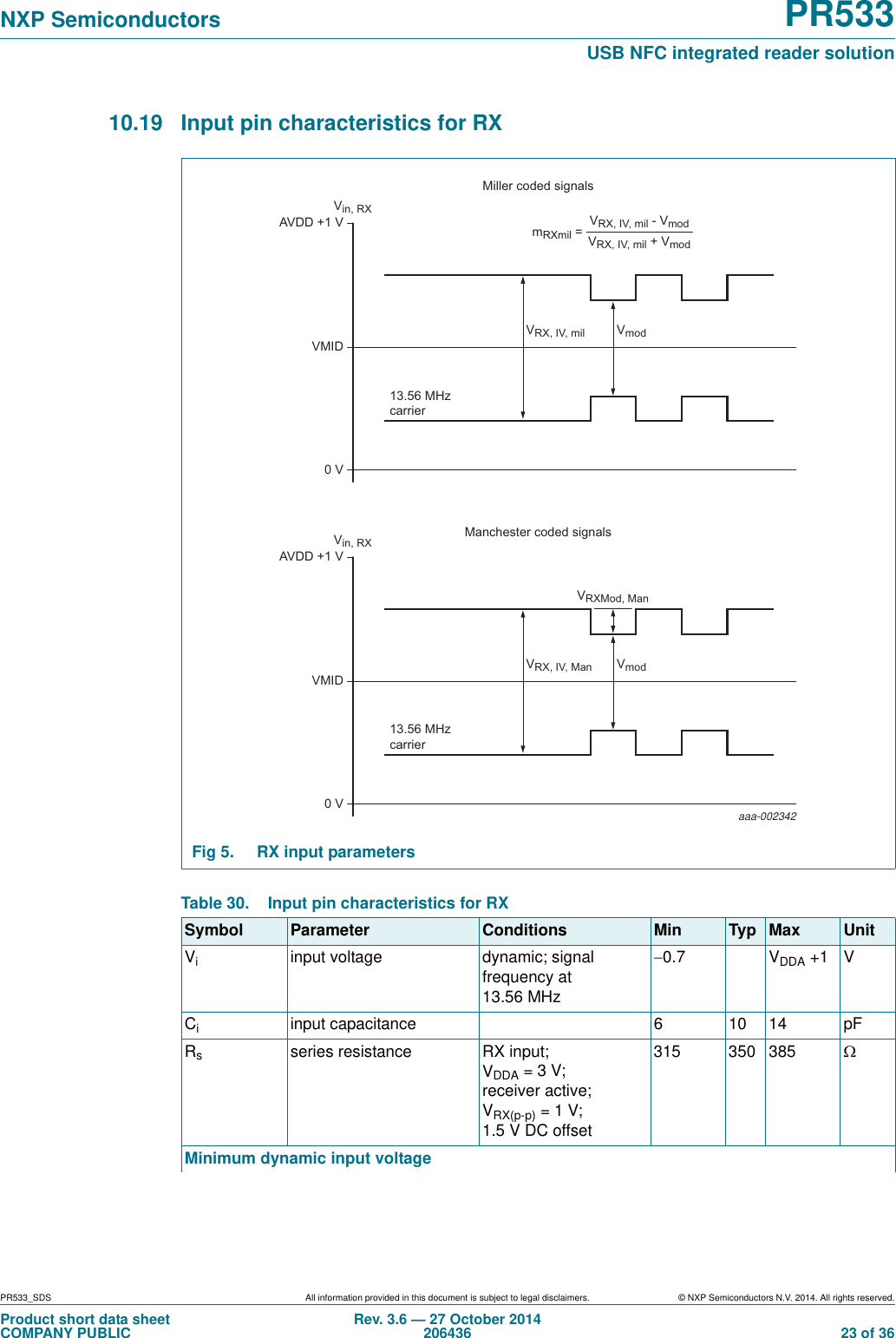
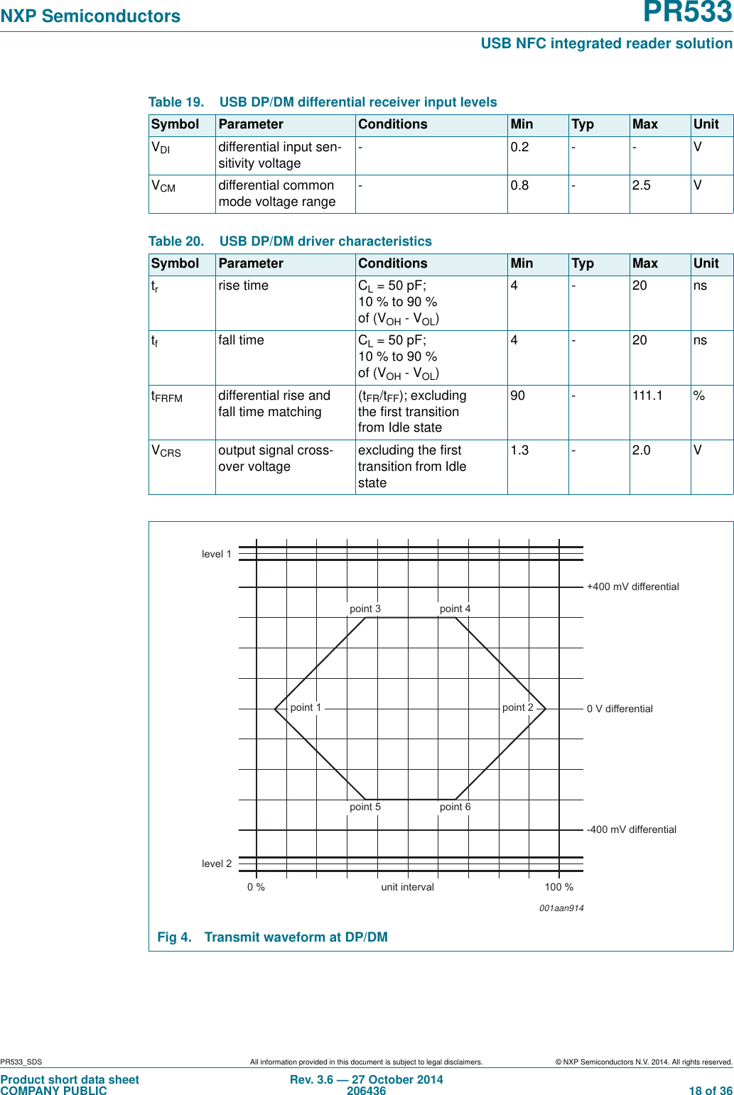
![PR533_SDS All information provided in this document is subject to legal disclaimers. © NXP Semiconductors N.V. 2014. All rights reserved.Product short data sheetCOMPANY PUBLICRev. 3.6 — 27 October 2014206436 24 of 36NXP Semiconductors PR533USB NFC integrated reader solution[1] The minimum modulation voltage is valid for all modulation schemes except Miller coded signals.10.20 Output pin characteristics for AUX1/AUX2 VRX(p-p) peak-to-peak receiver voltageMiller coded; 106 kbit/s-150500mVManchester coded; 212 kbit/s and 424 kbit/s-100200mVMaximum dynamic input voltageVRX(p-p) peak-to-peak receiver voltageMiller coded; 106 kbit/sVDDA -- VManchester coded; 212 and 424 kbit/sVDDA -- VMinimum modulation voltageVmod modulation voltage RxGain = 6 and 7 [1] --6mVRxGain = 4 and 5 [1] --18mVRxGain = 0 to 3 [1] --120mVMinimum modulation indexm modulation index Miller coded; 106 kbit/s VRX(p-p)=1.5V; SensMiller = 3-33-%Table 30. Input pin characteristics for RX …continuedSymbol Parameter Conditions Min Typ Max UnitTable 31. Output pin characteristics for AUX1/AUX2Symbol Parameter Conditions Min Typ Max UnitVOH HIGH-level output voltage VDDD =3V; IOH =4mAVDDD 0.4 - VDDD VVOL LOW-level output voltage VDDD =3V; IOL =4mAVSSD -VSSD +0.4 VIOH HIGH-level output current VDDD= 3 V; VOH = VDDD 0.34-- mAIOL LOW-level output current VDDD= 3 V; VOL = VDDD -0.34--mAILI input leakage current RSTPD_N = 0 V 1-+1ACiinput capacitance - 2.5 - pFCLload capacitance - - 15 pF](https://usermanual.wiki/Getac-Technology/PR533A.User-Manual-Module/User-Guide-3466028-Page-24.png)
![PR533_SDS All information provided in this document is subject to legal disclaimers. © NXP Semiconductors N.V. 2014. All rights reserved.Product short data sheetCOMPANY PUBLICRev. 3.6 — 27 October 2014206436 26 of 36NXP Semiconductors PR533USB NFC integrated reader solution10.22 System reset timing [1] Dependent on the 27.12 MHz crystal oscillator startup time.[2] If the trst pulse is shorter than 20 ns, the device may be only partially reset.Fig 6. System reset overviewtw(rst)trstVth(rst)reg + Vth(rst)reg(hys)Vth(rst)reg(hys)VDD(PVDD)RSTPD_NRSTOUT_NtPOR001aao394Table 34. Reset duration timeSymbol Parameter Conditions Min Typ Max UnittPOR power-on reset time [1] 0.1 0.4 2 mstrst reset time hard power-down time; user dependent [2] 20 - - nstw(rst) reset pulse width reset time when RSTPD_N is released [1] 0.1 0.4 2 ms](https://usermanual.wiki/Getac-Technology/PR533A.User-Manual-Module/User-Guide-3466028-Page-26.png)
![PR533_SDS All information provided in this document is subject to legal disclaimers. © NXP Semiconductors N.V. 2014. All rights reserved.Product short data sheetCOMPANY PUBLICRev. 3.6 — 27 October 2014206436 27 of 36NXP Semiconductors PR533USB NFC integrated reader solution10.23 Timing for the I2C-bus interface [1] The PR533 has a slope control according to the I2C-bus specification for the Fast mode. The slope control is always present and not dependent of the I2C-bus speed.[2] 27.12 MHz quartz starts in less than 800 s. For example, quartz like TAS-3225A, TAS-7 or KSS2F with appropriate layout.[3] The PR533 has an internal hold time of around 270 ns for the SDA signal to bridge the undefined region of the falling edge of P50_SCL.Fig 7. I2C-bus parametersTable 35. I2C-bus timing specificationSymbol Parameter Conditions Min Typ Max UnitfSCL SCL clock frequency 0 - 400 kHztHD;STA hold time (repeated) START condi-tionafter this period, the first clock pulse is generated600 - - nstSU;STA set-up time for a repeated START condition600 - - nstSU;STO set-up time for STOP condition 600 - - nstLOW LOW period of the SCL clock P50_SCL 1300 - - nstHIGH HIGH period of the SCL clock P50_SCL 600 - - nstHD;DAT data hold time 0 - 900 nstSU;DAT data set-up time 100 - - nstrrise time of both SDA and SCL sig-nalsP50_SCL [1] 20 - 300 nstffall time of both SDA and SCL sig-nalsP50_SCL [1] 20 - 300 nstBUF bus free time between a STOP and START condition1.3 - - mststretch stretch time stretching time on P50_SCL when woken-up on its own address[2] --1msthhold time internal for SDA 330 - 590 nsinternal for SDA in SPD mode[3] -270-ns001aaj635SDAtfSCLtLOW tftSP trtHD;STA tHD;DATtHD;STAtrtHIGHtSU;DATSSrPStSU;STAtSU;STOtBUF](https://usermanual.wiki/Getac-Technology/PR533A.User-Manual-Module/User-Guide-3466028-Page-27.png)
![PR533_SDS All information provided in this document is subject to legal disclaimers. © NXP Semiconductors N.V. 2014. All rights reserved.Product short data sheetCOMPANY PUBLICRev. 3.6 — 27 October 2014206436 28 of 36NXP Semiconductors PR533USB NFC integrated reader solution10.24 Temperature sensor [1] The temperature sensor embedded in the PR533 is not intended to monitor the temperature. Its purpose is to prevent destruction of the IC due to excessive heat. The external application should include circuitry to ensure that the ambient temperature does not exceed 85 C as specified in Table 5 “Operating conditions”.Table 36. Temperature sensor characteristicsSymbol Parameter Conditions Min Typ Max UnitTth(act)otp overtemperature protection acti-vation threshold temperature CIU [1] 100 125 140 C](https://usermanual.wiki/Getac-Technology/PR533A.User-Manual-Module/User-Guide-3466028-Page-28.png)
![PR533_SDS All information provided in this document is subject to legal disclaimers. © NXP Semiconductors N.V. 2014. All rights reserved.Product short data sheetCOMPANY PUBLICRev. 3.6 — 27 October 2014206436 30 of 36NXP Semiconductors PR533USB NFC integrated reader solution13. Revision history [1] Revision 3.4 is not available.Table 38. Revision historyDocument ID Release date Data sheet status Change notice SupersedesPR533_SDS v.3.6 20141027 Product short data sheet - PR533_SDS v.3.5Modifications: •Section 1.2 “Interfaces”: updatedPR533_SDS v.3.5[1] 20141003 Product short data sheet - PR533_SDS v.3.4Modifications: •Template updated.•Descriptive title updated.•Alternative descriptive title updated.PR533_SDS v.3.3 20121020 Product short data sheet - PR533_SDS v.3.2Modifications: •Section 14.4 “Licenses”: updatedPR533_SDS v.3.2 20120306 Product short data sheet - PR5331C3HN_SDS v.3.0Modifications: •Section 4 “Ordering information”: updated•General update to comply full data sheetPR5331C3HN_SDS v.3.0 20110803 Product short data sheet - -](https://usermanual.wiki/Getac-Technology/PR533A.User-Manual-Module/User-Guide-3466028-Page-30.png)
![PR533_SDS All information provided in this document is subject to legal disclaimers. © NXP Semiconductors N.V. 2014. All rights reserved.Product short data sheetCOMPANY PUBLICRev. 3.6 — 27 October 2014206436 31 of 36NXP Semiconductors PR533USB NFC integrated reader solution14. Legal information14.1 Data sheet status [1] Please consult the most recently issued document before initiating or completing a design. [2] The term ‘short data sheet’ is explained in section “Definitions”. [3] The product status of device(s) described in this document may have changed since this document was published and may differ in case of multiple devices. The latest product status information is available on the Internet at URL http://www.nxp.com. 14.2 DefinitionsDraft — The document is a draft version only. The content is still under internal review and subject to formal approval, which may result in modifications or additions. NXP Semiconductors does not give any representations or warranties as to the accuracy or completeness of information included herein and shall have no liability for the consequences of use of such information.Short data sheet — A short data sheet is an extract from a full data sheet with the same product type number(s) and title. A short data sheet is intended for quick reference only and should not be relied upon to contain detailed and full information. For detailed and full information see the relevant full data sheet, which is available on request via the local NXP Semiconductors sales office. In case of any inconsistency or conflict with the short data sheet, the full data sheet shall prevail.Product specification — The information and data provided in a Product data sheet shall define the specification of the product as agreed between NXP Semiconductors and its customer, unless NXP Semiconductors and customer have explicitly agreed otherwise in writing. In no event however, shall an agreement be valid in which the NXP Semiconductors product is deemed to offer functions and qualities beyond those described in the Product data sheet.14.3 DisclaimersLimited warranty and liability — Information in this document is believed to be accurate and reliable. However, NXP Semiconductors does not give any representations or warranties, expressed or implied, as to the accuracy or completeness of such information and shall have no liability for the consequences of use of such information. NXP Semiconductors takes no responsibility for the content in this document if provided by an information source outside of NXP Semiconductors.In no event shall NXP Semiconductors be liable for any indirect, incidental, punitive, special or consequential damages (including - without limitation - lost profits, lost savings, business interruption, costs related to the removal or replacement of any products or rework charges) whether or not such damages are based on tort (including negligence), warranty, breach of contract or any other legal theory. Notwithstanding any damages that customer might incur for any reason whatsoever, NXP Semiconductors’ aggregate and cumulative liability towards customer for the products described herein shall be limited in accordance with the Terms and conditions of commercial sale of NXP Semiconductors.Right to make changes — NXP Semiconductors reserves the right to make changes to information published in this document, including without limitation specifications and product descriptions, at any time and without notice. This document supersedes and replaces all information supplied prior to the publication hereof.Suitability for use — NXP Semiconductors products are not designed, authorized or warranted to be suitable for use in life support, life-critical or safety-critical systems or equipment, nor in applications where failure or malfunction of an NXP Semiconductors product can reasonably be expected to result in personal injury, death or severe property or environmental damage. NXP Semiconductors and its suppliers accept no liability for inclusion and/or use of NXP Semiconductors products in such equipment or applications and therefore such inclusion and/or use is at the customer’s own risk.Applications — Applications that are described herein for any of these products are for illustrative purposes only. NXP Semiconductors makes no representation or warranty that such applications will be suitable for the specified use without further testing or modification. Customers are responsible for the design and operation of their applications and products using NXP Semiconductors products, and NXP Semiconductors accepts no liability for any assistance with applications or customer product design. It is customer’s sole responsibility to determine whether the NXP Semiconductors product is suitable and fit for the customer’s applications and products planned, as well as for the planned application and use of customer’s third party customer(s). Customers should provide appropriate design and operating safeguards to minimize the risks associated with their applications and products. NXP Semiconductors does not accept any liability related to any default, damage, costs or problem which is based on any weakness or default in the customer’s applications or products, or the application or use by customer’s third party customer(s). Customer is responsible for doing all necessary testing for the customer’s applications and products using NXP Semiconductors products in order to avoid a default of the applications and the products or of the application or use by customer’s third party customer(s). NXP does not accept any liability in this respect.Limiting values — Stress above one or more limiting values (as defined in the Absolute Maximum Ratings System of IEC 60134) will cause permanent damage to the device. Limiting values are stress ratings only and (proper) operation of the device at these or any other conditions above those given in the Recommended operating conditions section (if present) or the Characteristics sections of this document is not warranted. Constant or repeated exposure to limiting values will permanently and irreversibly affect the quality and reliability of the device.Terms and conditions of commercial sale — NXP Semiconductors products are sold subject to the general terms and conditions of commercial sale, as published at http://www.nxp.com/profile/terms, unless otherwise agreed in a valid written individual agreement. In case an individual agreement is concluded only the terms and conditions of the respective agreement shall apply. NXP Semiconductors hereby expressly objects to applying the customer’s general terms and conditions with regard to the purchase of NXP Semiconductors products by customer.No offer to sell or license — Nothing in this document may be interpreted or construed as an offer to sell products that is open for acceptance or the grant, conveyance or implication of any license under any copyrights, patents or other industrial or intellectual property rights.Document status[1][2] Product status[3] DefinitionObjective [short] data sheet Development This document contains data from the objective specification for product development. Preliminary [short] data sheet Qualification This document contains data from the preliminary specification. Product [short] data sheet Production This document contains the product specification.](https://usermanual.wiki/Getac-Technology/PR533A.User-Manual-Module/User-Guide-3466028-Page-31.png)
![PR533_SDS All information provided in this document is subject to legal disclaimers. © NXP Semiconductors N.V. 2014. All rights reserved.Product short data sheetCOMPANY PUBLICRev. 3.6 — 27 October 2014206436 34 of 36NXP Semiconductors PR533USB NFC integrated reader solution16. TablesTable 1. Quick reference data . . . . . . . . . . . . . . . . . . . . .3Table 2. Ordering information . . . . . . . . . . . . . . . . . . . . .4Table 3. PR533 pin description . . . . . . . . . . . . . . . . . . . .5Table 4. Limiting values . . . . . . . . . . . . . . . . . . . . . . . . . .7Table 5. Operating conditions . . . . . . . . . . . . . . . . . . . . .8Table 6. Thermal characteristics . . . . . . . . . . . . . . . . . . .8Table 7. Current consumption characteristics . . . . . . . . .9Table 8. Voltage regulator characteristics[1] . . . . . . . . . . .9Table 9. Antenna presence detection. . . . . . . . . . . . . . .10Table 10. Crystal requirements. . . . . . . . . . . . . . . . . . . . . 11Table 11. Pin characteristics for 27.12 MHz XTAL Oscillator (OSCIN, OSCOUT). . . . . . . . . . . . . . 11Table 12. RSTPD_N input pin characteristics . . . . . . . . .12Table 13. Input pin characteristics for I0, I1 and TESTEN . . . . . . . . . . . . . . . . . . . . . . . . . . . . .12Table 14. RSTOUT_N output pin characteristics . . . . . . .13Table 15. Input/output pin characteristics for pin P70_IRQ . . . . . . . . . . . . . . . . . . . . . . . . . . .14Table 16. Input/output pin characteristics for P30 / UART_RX, P31 / UART_TX, P32_INT0, P33_INT1 . . . . . . . . . . . . . . . . . . . . . . . . . . . . .15Table 17. Input/output pin characteristics for P35 . . . . . .16Table 18. Input/output pin characteristics for DP and DM for USB interface. . . . . . . . . . . . . . . . .17Table 19. USB DP/DM differential receiver input levels . .18Table 20. USB DP/DM driver characteristics . . . . . . . . . .18Table 21. Input Pin characteristics for DP for HSUinterface . . . . . . . . . . . . . . . . . . . . . . . . . . . . . .19Table 22. Output Pin characteristics for DM for HSU interface . . . . . . . . . . . . . . . . . . . . . . . . . . . . . .19Table 23. Input/output drain output pin characteristics for SCL I2C interface. . . . . . . . . . . . . . . . . . . . .20Table 24. Input/output drain output pin characteristics for SDA I2C interface . . . . . . . . . . . . . . . . . . . .20Table 25. Output pin characteristics for DELATT . . . . . . .21Table 26. Input/output pin characteristics for SIGIN. . . . .21Table 27. Output pin characteristics for SIGOUT . . . . . . .21Table 28. Input/output pin characteristics for P34 . . . . . .22Table 29. Output pin characteristics for LOADMOD . . . .22Table 30. Input pin characteristics for RX . . . . . . . . . . . .23Table 31. Output pin characteristics for AUX1/AUX2 . . .24Table 32. Output pin characteristics for TX1/TX2. . . . . . .25Table 33. Output resistance for TX1/TX2 . . . . . . . . . . . . .25Table 34. Reset duration time . . . . . . . . . . . . . . . . . . . . .26Table 35. I2C-bus timing specification . . . . . . . . . . . . . . .27Table 36. Temperature sensor characteristics . . . . . . . . .28Table 37. Abbreviations . . . . . . . . . . . . . . . . . . . . . . . . . .29Table 38. Revision history . . . . . . . . . . . . . . . . . . . . . . . .30](https://usermanual.wiki/Getac-Technology/PR533A.User-Manual-Module/User-Guide-3466028-Page-34.png)