Getac Technology PR533A RFID module User Manual PR533 USB NFC integrated reader solution
Getac Technology Corporation RFID module PR533 USB NFC integrated reader solution
Contents
- 1. User Manual Host
- 2. User Manual Module
User Manual Module

1. General description
The PR5331C3HN is a highly integrated transceiver module for contactless reader/writer
communication at 13.56 MHz.
A dedicated ROM code is implemented to handle different RF protocols by an integrated
microcontroller. The system host controller communicates with the PR5331C3HN by
using the USB or the HSU link.
The protocol between the host controller and the PR5331C3HN, on top of this physical
link is the CCID protocol.
1.1 RF protocols
PR5331C3HN supports the PCD mode for FeliCa (212 kbps and 424 kbps),
ISO/IEC14443 Type A and B (from 106 kbps to 848 kbps), MIFARE (106 kbps), B' cards
(106 kbps), picoPass tag (106 kbps) and Innovision Jewel cards (106 kbps)
The Initiator passive mode (from 106 kbps to 424 kbps) can be supported through the
PC/SC transparent mode.
1.2 Interfaces
The PR5331C3HN supports a USB 2.0 full speed interface (bus powered or host powered
mode).
Alternatively to the USB interface, a High Speed UART (from 9600b up to 1.2 Mb) can be
used to connect the PR533 to a host.
The PR5331C3HN has also a master I2C-bus interface that allows to connect one of the
following peripherals:
•An external EEPROM: in this case the PR5331C3HN is configured as master and is
able to communicate with external EEPROM (address A0h) which can store
configuration data like PID, UID and RF parameters. When a USB host interface is
used, these parameters are retrieved from the EEPROM at startup of the device
•A TDA8029 contact smart card reader
1.3 Standards compliancy
PR5331C3HN offers commands in order for applications to be compliant with “EMV
Contactless Communication Protocol Specification V2.0.1”.
PR5331C3HN supports RF protocols ISO/IEC 14443A and B such as compliancy with
Smart eID standard can be achieved at application level.
PR533
USB NFC integrated reader solution
Rev. 3.6 — 27 October 2014
206436
Product short data sheet
COMPANY PUBLIC

PR533_SDS All information provided in this document is subject to legal disclaimers. © NXP Semiconductors N.V. 2014. All rights reserved.
Product short data sheet
COMPANY PUBLIC
Rev. 3.6 — 27 October 2014
206436 2 of 36
NXP Semiconductors PR533
USB NFC integrated reader solution
Support of USB 2.0 full speed, interoperable with USB 3.0 hubs.
The PR533C3HN in PCD mode is compliant with EMV contactless specification V2.0.1.
1.4 Supported operating systems
•Microsoft Windows 2000
•Microsoft Windows XP (32 and 64 bits)
•Microsoft Windows 2003 Server (32 and 64 bits)
•Microsoft Windows 2008 Server (32 and 64 bits)
•Microsoft Windows Vista (32 and 64 bits)
•Microsoft Windows 7 (32 and 64 bits)
The PR533 is supported by the following OS through the PCSC-Lite driver:
•GNU/Linux using libusb 1.0.x and later
•Mac OS Leopard (1.5.6 and newer)
•Mac OS Snow Leopard (1.6.X)
•Solaris
•FreeBSD
2. Features and benefits
USB 2.0 full speed host interface and CCID protocol support
Integrated microcontroller implements high-level RF protocols
Buffered output drivers to connect an antenna with minimum number of external
components
Integrated RF level detector
Integrated data mode detector
Supports ISO/IEC 14443A Reader/Writer mode up to 848 kbit/s
Supports ISO/IEC 14443B Reader/Writer mode up to 848 kbit/s
Supports contactless communication according to the FeliCa protocol at 212 kbit/s and
424 kbit/s
Supports MIFARE encryption
Typical operating distance in Read/Write mode for communication to
ISO/IEC 14443A/MIFARE, ISO/IEC 14443B or FeliCa cards up to 50 mm depending
on antenna size and tuning
I2C-bus master interface allows to connect an external I2C EEPROM for configuration
data storage or to control a TDA8029 contact smart card reader
Low-power modes
Hard power-down mode
Soft power-down mode
Only one external oscillator required (27.12 MHz Crystal oscillator)
Power modes
USB bus power mode
2.5 V to 3.6 V power supply operating range in non-USB bus power mode
PR533_SDS All information provided in this document is subject to legal disclaimers. © NXP Semiconductors N.V. 2014. All rights reserved.
Product short data sheet
COMPANY PUBLIC
Rev. 3.6 — 27 October 2014
206436 3 of 36
NXP Semiconductors PR533
USB NFC integrated reader solution
Dedicated I/O ports for external device control
3. Quick reference data
[1] VDDD, VDDA and VDD(TVDD) must always be at the same supply voltage.
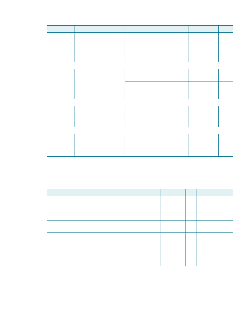
Table 1. Quick reference data
Symbol Parameter Conditions Min Typ Max Unit
VBUS bus supply voltage 4.02 5 5.25 V
(non-USB mode);
VBUS =V
DDD; VSSD =0V
2.5 3.3 3.6 V
VDDA analog supply voltage VDDA = VDDD = VDD(TVDD) =
VDD(PVDD); VSSA = VSSD =
VSS(PVSS) = VSS(TVSS) = 0 V
[1] 2.5 3.3 3.6 V
VDDD digital supply voltage [1] 2.5 3.3 3.6 V
VDD(TVDD) TVDD supply voltage [1] 2.5 3.3 3.6 V
VDD(PVDD) PVDD supply voltage 1.6 - 3.6 V
VDD(SVDD) SVDD supply voltage VSSA = VSSD = VSS(PVSS) =
VSS(TVSS) = 0 V; reserved for
future use
VDDD 0.1 - VDDD V
IBUS bus supply current maximum load current (USB
mode); measured on VBUS
150 mA
maximum inrush current lim-
itation; at power-up
(curlimoff = 0)
100 mA
Ipd power-down current VDDA = VDDD = VDD(TVDD) = VDD(PVDD) = 3 V; not powered from USB
hard power-down;
RF level detector off
10 A
soft power-down; RF level
detector on
30 A
ICCSL suspended low-power
device supply current
RF level detector on, (with-
out resistor on DP/DM)
--250A
IDDD digital supply current RF level detector on,
VDD(SVDD) switch off
[1] -15-mA
IDD(SVDD) SVDD supply current VDDS = 3 V - - 30 mA
IDDA analog supply current RF level detector on - 6 - mA
IDD(TVDD) TVDD supply current during RF transmission;
VDD(TVDD) =3 V
-60100mA
Ptot total power dissipation Tamb =30 to +85 C--0.55W
Tamb ambient temperature 30 - +85 C
PR533_SDS All information provided in this document is subject to legal disclaimers. © NXP Semiconductors N.V. 2014. All rights reserved.
Product short data sheet
COMPANY PUBLIC
Rev. 3.6 — 27 October 2014
206436 4 of 36
NXP Semiconductors PR533
USB NFC integrated reader solution
4. Ordering information
[1] 60 or 70 refers to the ROM code version described in the User Manual. For differences of romcode versions refer to the release note of
the product.
[2] Refer to Section 14.4 “Licenses”.
[3] MSL 2 (Moisture Sensitivity Level).
5. Block diagram
The following block diagram describes hardware blocks controlled by PR5331C3HN
firmware or which can be accessible for data transaction by a host baseband.
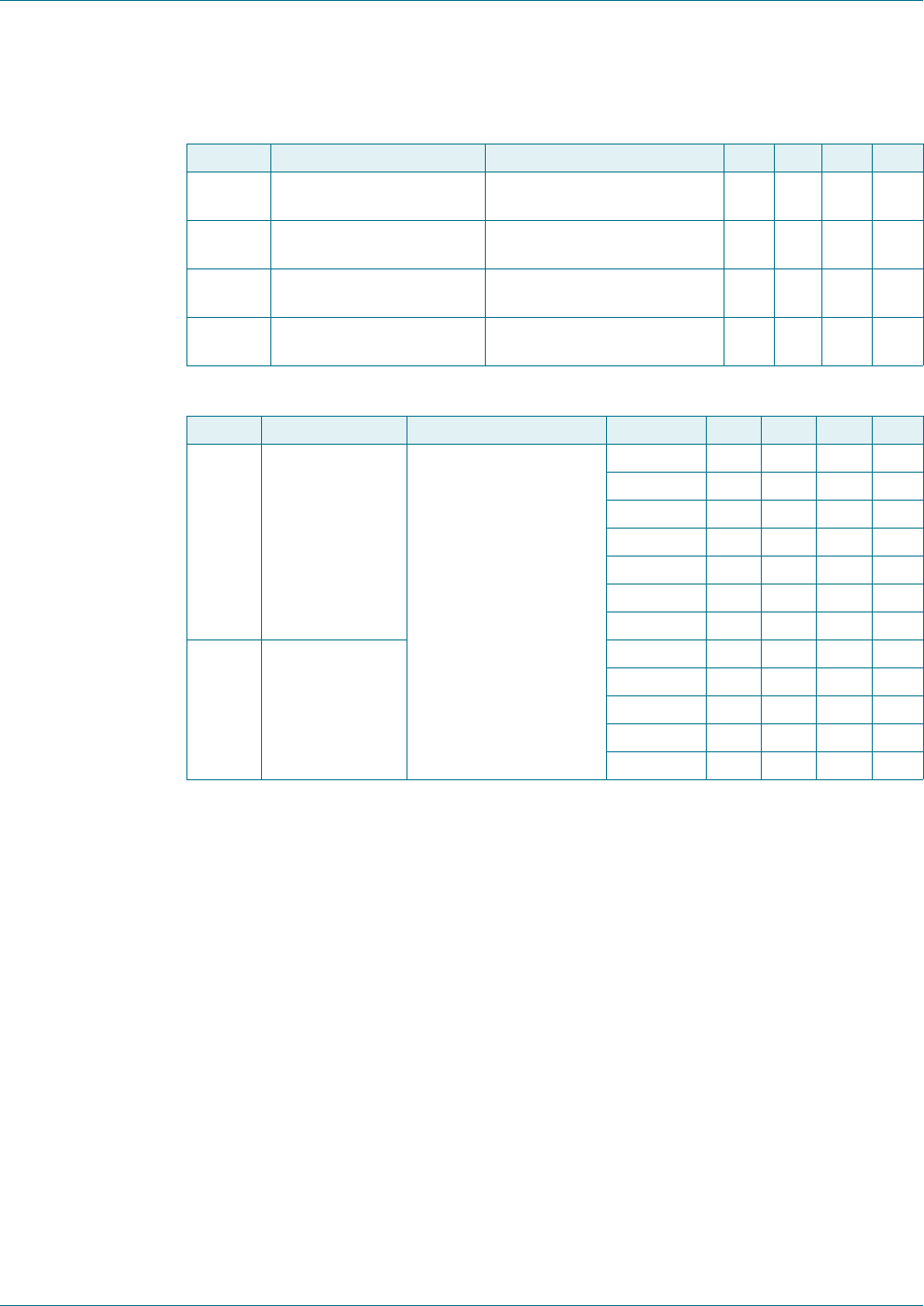
Table 2. Ordering information
Type number Package
Name Description Version
PR5331C3HN/C360[1][2][3] HVQFN40 plastic thermal enhanced very thin quad flat package; no leads;
40 terminals; body 6 6 0.85 mm
SOT618-1
PR5331C3HN/C370[1][2][3]
Fig 1. Block diagram
aaa-000043
SUPPLY
SUPERVISOR
27 MHz OSC
AND
FRAC N
PLL
SVDD
SWITCH
NFC
ANALOG
FRONT END
AND
CLUART
80C51 CPU
44 k ROM
1.2 k BYTES RAM
USB
DEVICE
I
2
C
MASTER
MATX
RSTPD_N
PVDD
SVDD
VBUS
P30 P31 P32_INT0
GPIOs
P33_INT0 P35
RSTOUT_N DVDD P70_IRQ AVSS
DVSS
OSCIN
OSCOUT
I0
I1
SDA
P50_SCL
DELATT
48 MHz
SIGIN
SIGOUT
P34
TVDD
AVDD
RX
VMID
TX1
TVSS
TX2
REGULATOR
3.3 V
PCR
PR533_SDS All information provided in this document is subject to legal disclaimers. © NXP Semiconductors N.V. 2014. All rights reserved.
Product short data sheet
COMPANY PUBLIC
Rev. 3.6 — 27 October 2014
206436 5 of 36
NXP Semiconductors PR533
USB NFC integrated reader solution
6. Pinning information
6.1 Pinning
6.2 Pin description
Fig 2. Pin configuration for HVQFN 40 (SOT618-1)
aaa-000044
PR533
P70_IRQ
VMID
RX
RSTOUT_N
AVDD DVSS
TVSS2 DM
TX2 DP
TVDD PVDD
TX1 DELATT
TVSS1 P30
LOADMOD P31
DVSS P32_INT0
AVSS
AUX1
AUX2
DVSS
OSCIN
OSCOUT
I0
I1
TESTEN
P35
VBUS
DVDD
RSTPD_N
SVDD
SIGIN
SIGOUT
P34
SDA
P50_SCL
P33_INT1
10 21
922
823
724
625
526
427
328
229
130
11
12
13
14
15
16
17
18
19
20
40
39
38
37
36
35
34
33
32
31
terminal 1
index area
Transparent top view
Table 3. PR533 pin description
Symbol Pin Type Pad ref
voltage
Description
DVSS 1 G digital ground
LOADMOD 2 O DVDD load modulation output provides digital signal for FeliCa and MIFARE card
operating mode
TVSS1 3 G transmitter ground: supplies the output stage of TX1
TX1 4 O TVDD transmitter 1: transmits modulated 13.56 MHz energy carrier
TVDD 5 P transmitter power supply: supplies the output stage of TX1 and TX2
TX2 6 O TVDD transmitter 2: delivers the modulated 13.56 MHz energy carrier
TVSS2 7 G transmitter ground: supplies the output stage of TX2
AVDD 8 P analog power supply
VMID 9 P AVDD internal reference voltage: This pin delivers the internal reference voltage.
RX 10 I AVDD receiver input: Input pin for the reception signal, which is the load modulated
13.56 MHz energy carrier from the antenna circuit
AVSS 11 G analog ground
AUX1 12 O DVDD auxiliary output 1: This pin delivers analog and digital test signals
AUX2 13 O DVDD auxiliary output 2: This pin delivers analog and digital test signals
DVSS 14 G digital ground

PR533_SDS All information provided in this document is subject to legal disclaimers. © NXP Semiconductors N.V. 2014. All rights reserved.
Product short data sheet
COMPANY PUBLIC
Rev. 3.6 — 27 October 2014
206436 6 of 36
NXP Semiconductors PR533
USB NFC integrated reader solution
OSCIN 15 I AVDD crystal oscillator input: input to the inverting amplifier of the oscillator. This pin
is also the input for an externally generated clock (fclk = 27.12 MHz).
OSCOUT 16 O AVDD crystal oscillator output: output of the inverting amplifier of the oscillator.
I0 17 I DVDD interface mode lines: selects the used host interface; in test mode I0 is used
as test signals.
I1 18 I DVDD
TESTEN 19 I DVDD test enable pin:
when set to 1 enable the test mode.
when set to 0 reset the TCB and disable the access to the test mode.
P35 20 I/O DVDD general purpose I/O signal
P70_IRQ 21 I/O PVDD interrupt request: output to signal an interrupt event to the host (Port 7 bit 0)
RSTOUT_N 22 O PVDD output reset signal; when LOW it indicates that the circuit is in reset state.
DVSS 23 G digital ground
DM 24 I/O PVDD USB D data line in USB mode or TX in HSU mode; in test mode this signal
is used as input and output test signal
DP 25 I/O PVDD USB D+ data line in USB mode or RX in HSU mode; in test mode this signal
is used as input and output test signal.
PVDD 26 P I/O pad power supply
DELATT 27 O PVDD optional output for an external 1.5 k resistor connection on D+.
P30 28 I/O PVDD general purpose I/O signal. Can be configured to act either as RX line of the
second serial interface UART or general purpose I/O.
In test mode this signal is used as input and output test signal.
P31 29 I/O PVDD general purpose I/O signal. Can be configured to act either as TX line of the
second serial interface UART or general purpose I/O.
In test mode this signal is used as input and output test signal.
P32_INT0 30 I/O PVDD general purpose I/O signal. Can also be used as an interrupt source
In test mode this signal is used as input and output test signal.
P33_INT1 31 I/O PVDD general purpose I/O signal. Can be used to generate an HZ state on the out-
put of the selected interface for the Host communication and to enter into
power-down mode without resetting the internal state of PR533.
In test mode this signal is used as input and output test signal.
P50_SCL 32 I/O DVDD I2C-bus clock line - open-drain in output mode
SDA 33 I/O DVDD I2C-bus data line - open-drain in output mode
P34 34 I/O SVDD general purpose I/O signal or clock signal for the SAM
SIGOUT 35 O SVDD contactless communication interface output: delivers a serial data stream
according to NFCIP-1 and output signal for the SAM.
In test mode this signal is used as test signal output.
SIGIN 36 I SVDD contactless communication interface input: accepts a digital, serial data
stream according to NFCIP-1 and input signal from the SAM.
In test mode this signal is used as test signal input.
SVDD 37 P output power for SAM power supply. Switched on by Firmware with an over-
load detection. Used as a reference voltage for SAM communication.
Table 3. PR533 pin description …continued
Symbol Pin Type Pad ref
voltage
Description
PR533_SDS All information provided in this document is subject to legal disclaimers. © NXP Semiconductors N.V. 2014. All rights reserved.
Product short data sheet
COMPANY PUBLIC
Rev. 3.6 — 27 October 2014
206436 7 of 36
NXP Semiconductors PR533
USB NFC integrated reader solution
[1] Pin types: I= Input, O = Output, I/O = Input/Output, P = Power and G = Ground.
7. Limiting values
[1] 1500 , 100 pF; EIA/JESD22-A114-A
[2] 0.75 mH, 200 pF; EIA/JESD22-A115-A
[3] Field induced model; EIA/JESC22-C101-C
RSTPD_N 38 I PVDD reset and power-down: When LOW, internal current sources are switched off,
the oscillator is inhibited, and the input pads are disconnected from the out-
side world.
With a negative edge on this pin the internal reset phase starts.
DVDD 39 P digital power supply
VBUS 40 P USB power supply.
Table 3. PR533 pin description …continued
Symbol Pin Type Pad ref
voltage
Description
Table 4. Limiting values
In accordance with the Absolute Maximum Rating System (IEC 60134).
Symbol Parameter Conditions Min Max Unit
VDDA analog supply voltage 0.5 +4 V
VDDD digital supply voltage 0.5 +4 V
VDD(TVDD) TVDD supply voltage 0.5 +4 V
VDD(PVDD) PVDD supply voltage 0.5 +4 V
VDD(SVDD) SVDD supply voltage 0.5 +4 V
VBUS bus supply voltage 0.5 +5.5 V
Ptot total power dissipation - 500 mW
IDD(SVDD) SVDD supply current maximum current in VDDS
switch
-30 mA
Viinput voltage TX1, TX2, RX pins 0.5 +4 V
VESD electrostatic discharge voltage HBM [1] 2.0 kV
MM [2] -200V
CDM [3] -1kV
Tstg storage temperature 55 +150 C
Tjjunction temperature 40 +125 C
Vi(dyn)(RX) dynamic input voltage on pin RX input signal at 13.56 MHz 0.7 VDD(AVDD) +1.0 V
Vi(dyn)(TX1) dynamic input voltage on pin TX1 input signal at 13.56 MHz 1.2 VDD(TVDD) +1.3 V
Vi(dyn)(TX2) dynamic input voltage on pin TX2 input signal at 13.56 MHz 1.2 VDD(TVDD) +1.3 V
ITX1 current on pin TX1 output signal at 13.56 MHz 300 +300 mA
ITX2 current on pin TX2 output signal at 13.56 MHz 300 +300 mA
PR533_SDS All information provided in this document is subject to legal disclaimers. © NXP Semiconductors N.V. 2014. All rights reserved.
Product short data sheet
COMPANY PUBLIC
Rev. 3.6 — 27 October 2014
206436 8 of 36
NXP Semiconductors PR533
USB NFC integrated reader solution
8. Recommended operating conditions
[1] VSSA, VDDD and VDD(TVDD) shall always be on the same voltage level.
[2] Supply voltages below 3 V reduces the performance (e.g. the achievable operating distance).
9. Thermal characteristics
10. Characteristics
Unless otherwise specified, the limits are given for the full operating conditions. The
typical value is given for 25 C, VDDD = 3.4 V and VDD(PVDD) = 3 V in non-USB bus power
mode, VBUS = 5 V in USB power mode.
Timings are only given from characterization results.
10.1 Power management characteristics
10.1.1 Current consumption characteristics
Typical value using a complementary driver configuration and an antenna matched to
40 between TX1 and TX2 at 13.56 MHz.
Table 5. Operating conditions
Symbol Parameter Conditions Min Typ Max Unit
VBUS bus supply voltage VSSA = VSSD = VSS(PVSS) = VSS(TVSS) = 0 V 4.02 5 5.25 V
supply voltage (non-USB mode); VBUS = VDDD;
VSSA = VSSD = VSS(PVSS) = VSS(TVSS) = 0 V
2.53.3 3.6V
VDDA analog supply volt-
age
VDDA = VDDD = VDD(TVDD) = VDD(PVDD);
VSSA =V
SSD = VSS(PVSS) = VSS(TVSS) = 0 V
[1][2] 2.53.3 3.6V
VDDD digital supply volt-
age
VDDA = VDDD = VDD(TVDD) = VDD(PVDD);
VSSA =V
SSD = VSS(PVSS) = VSS(TVSS) = 0 V
[1][2] 2.53.3 3.6V
VDD(TVDD) TVDD supply volt-
age
VDDA = VDDD = VDD(TVDD) = VDD(PVDD);
VSSA =V
SSD = VSS(PVSS) = VSS(TVSS) = 0 V
[1][2] 2.53.3 3.6V
VDD(PVDD) PVDD supply volt-
age
supply pad for host interface;
VDDA =V
DDD =V
DD(TVDD) = VDD(PVDD);
VSSA =V
SSD = VSS(PVSS) = VSS(TVSS) = 0 V
[2] 1.6 1.8 to 3.3 3.6 V
Tamb ambient tempera-
ture
30 +25 +85 C
Table 6. Thermal characteristics
Symbol Parameter Conditions Min Typ Max Unit
Rth(j-a) thermal resistance from
junction to ambient
in free air with exposed pad
soldered on a 4 layer Jedec
PCB-0.5
-3741.1K/W
PR533_SDS All information provided in this document is subject to legal disclaimers. © NXP Semiconductors N.V. 2014. All rights reserved.
Product short data sheet
COMPANY PUBLIC
Rev. 3.6 — 27 October 2014
206436 9 of 36
NXP Semiconductors PR533
USB NFC integrated reader solution
[1] Ipd is the total currents over all supplies.
[2] IDD(PVDD) depends on the overall load at the digital pins.
[3] IDD(SVDD) depends on the overall load on VDD(SVDD) pad.
[4] IDD(TVDD) depends on VDD(TVDD) and the external circuitry connected to TX1 and TX2.
[5] During operation with a typical circuitry the overall current is below 100 mA.
10.1.2 Voltage regulator characteristics
[1] The internal regulator is only enabled when the USB interface is selected by I0 and I1.
10.2 Antenna presence self test thresholds
The values in Ta ble 9 are guaranteed by design. Only functional is done in production for
cases andet_ithl[1:0] = 10b and for andet_ithh[2:0] = 011b.
Table 7. Current consumption characteristics
Symbol Parameter Conditions Min Typ Max Unit
Ipd power-down current VDDA = VDDD = VDD(TVDD) = VDD(PVDD) = 3 V; not powered from USB
hard power-down current; not powered
from USB; RF level detector off
[1] -1.310A
soft power-down current; not powered
from USB; RF level detector on
[1] -930A
ICCSL suspended low-power device
supply current
VBUS =5V; V
DDA = VDDD = VDD(TVDD) =
VDD(PVDD) =3V; V
DDS = 0 V; RF level
detector on (without resistor on pin DP
(D+))
[1] - 120 250 A
IDDD digital supply current VDDA = VDDD = VDD(TVDD) = VDD(PVDD)
= 3 V; RF level detector on
-12- mA
IDDA analog supply current VDDA = VDDD = VDD(TVDD) = VDD(PVDD) =3V
RF level detector on - 3 6 mA
RF level detector off - 1.5 5 mA
IDD(PVDD) PVDD supply current [2] --30mA
IDD(SVDD) SVDD supply current sam_switch_en set to 1 [3] --30mA
IDD(TVDD) TVDD supply current continuous wave; VDD(TVDD) =3V [4][5] - 60 100 mA
Table 8. Voltage regulator characteristics[1]
Symbol Parameter Conditions Min Typ Max Unit
VBUS bus supply voltage USB mode; VSS = 0 V 4.02 5 5.25 V
VDDD digital supply voltage after inrush current limitation (USB
mode); from IVDDD = 0 mA to
IVDDD =150mA
2.95 3.3 3.6 V
IBUS bus supply current USB mode; measure on VBUS --150mA
Iinrush(lim) inrush current limit at power-up (curlimofff = 0) - - 100 mA
Vth(rst)reg regulator reset threshold voltage regulator reset 1.90 2.15 2.40 V
Vth(rst)reg(hys) regulator reset threshold voltage
hysteresis
35 60 85 mV
VDDD decoupling capacitor 8 10 - F
PR533_SDS All information provided in this document is subject to legal disclaimers. © NXP Semiconductors N.V. 2014. All rights reserved.
Product short data sheet
COMPANY PUBLIC
Rev. 3.6 — 27 October 2014
206436 10 of 36
NXP Semiconductors PR533
USB NFC integrated reader solution
Table 9. Antenna presence detection
Parameter Conditions Min Typ Max Unit
IVDDD lower current threshold for antenna presence detection
andet_ithl[1:0] 00b - 5 - mA
01b - 15 - mA
10b - 25 - mA
11b - 35 - mA
IVDDD upper current threshold for antenna presence detection
andet_ithh[2:0] 000b - 45 - mA
001b - 60 - mA
010b - 75 - mA
011b - 90 - mA
100b - 105 - mA
101b - 120 - mA
110b - 135 - mA
111b - 150 - mA
PR533_SDS All information provided in this document is subject to legal disclaimers. © NXP Semiconductors N.V. 2014. All rights reserved.
Product short data sheet
COMPANY PUBLIC
Rev. 3.6 — 27 October 2014
206436 11 of 36
NXP Semiconductors PR533
USB NFC integrated reader solution
10.3 Typical 27.12 MHz Crystal requirements
10.4 Pin characteristics for 27.12 MHz XTAL Oscillator (OSCIN, OSCOUT)
[1] n(th) and fn(th) define the mask for maximum acceptable phase noise of the clock signal at the OSCIN, OSCOUT inputs. See Figure 3
“27.12 MHz input clock phase noise spectrum mask”.
Table 10. Crystal requirements
Symbol Parameter Conditions Min Typ Max Unit
fxtal crystal frequency 27.107 27.12 27.133 MHz
ESR equivalent series resistance - - 100
CLload capacitance - 10 - pF
Pxtal crystal power dissipation 100 - - W
Table 11. Pin characteristics for 27.12 MHz XTAL Oscillator (OSCIN, OSCOUT)
Symbol Parameter Conditions Min Typ Max Unit
ILI input leakage current RSTPD_N = 0 V 1-+1mA
VIH HIGH-level input voltage 0.7 VDDA -V
DDA V
VIL LOW-level input voltage 0 - 0.3 VDDA V
VOH HIGH-level output voltage - 1.1 - V
VOL LOW-level output voltage - 0.2 - V
fclk clock frequency 0.05 % 27.12 +0.05 % MHz
duty cycle 40 50 60 %
n(th) phase noise threshold [1] --140 dBc/Hz
fn(th) phase noise threshold fre-
quency
n(th) = 140dBc/Hz;
20dB/decade slope
[1] - - 50 kHz
OSCIN
Viinput voltage DC - 0.65 - V
Ciinput capacitance VDDA = 2.8 V; Vi(DC) = 0.65 V;
Vi(AC) = 1 V p-p
-2-pF
OSCOUT
Ciinput capacitance - 2 - pF
Fig 3. 27.12 MHz input clock phase noise spectrum mask
φn(th)
phase noise
(dBc/Hz)
-20 dB/decade acceptable phase
noise area
001aao393
fφn(th) frequency (Hz)
PR533_SDS All information provided in this document is subject to legal disclaimers. © NXP Semiconductors N.V. 2014. All rights reserved.
Product short data sheet
COMPANY PUBLIC
Rev. 3.6 — 27 October 2014
206436 12 of 36
NXP Semiconductors PR533
USB NFC integrated reader solution
10.5 RSTPD_N input pin characteristics
10.6 Input pin characteristics for I0, I1 and TESTEN
[1] To minimize power consumption when in soft power-down mode, the limit is VDDD 0.4 V.
[2] To minimize power consumption when in soft power-down mode, the limit is 0.4 V.
[3] TESTEN should never be set to high level in the application. It is used for production test purpose only. It is
recommended to connect TESTEN to ground although there is a pull-down included.
Table 12. RSTPD_N input pin characteristics
Symbol Parameter Conditions Min Typ Max Unit
VIH HIGH-level input volt-
age
VDD(PVDD) 0.4 - VDD(PVDD) V
VIL LOW-level input volt-
age
0-0.4V
IIH HIGH-level input cur-
rent
VI=V
DD(PVDD) 1-1A
IIL LOW-level input current VI = 0 V 1-1A
Ciinput capacitance - 2.5 - pF
Table 13. Input pin characteristics for I0, I1 and TESTEN
Symbol Parameter Conditions Min Typ Max Unit
VIH HIGH-level input voltage [1] 0.7 VDDD -V
DDD V
VIL LOW-level input voltage [2] 00.3VDDD V
IIH HIGH-level input current I0 and I1;
VI=V
DDD
[3] 1-1 A
IIL LOW-level input current VI=0V 1-1 A
Ciinput capacitance - 2.5 - pF
PR533_SDS All information provided in this document is subject to legal disclaimers. © NXP Semiconductors N.V. 2014. All rights reserved.
Product short data sheet
COMPANY PUBLIC
Rev. 3.6 — 27 October 2014
206436 13 of 36
NXP Semiconductors PR533
USB NFC integrated reader solution
10.7 RSTOUT_N output pin characteristics
[1] Data at VDD(PVDD) = 1.8V are only given from characterization results.
[2] IOH and IOL give the output drive capability from which the rise and fall times may be calculated as a function of the load capacitance.
Table 14. RSTOUT_N output pin characteristics
Symbol Parameter Conditions Min Typ Max Unit
VOH HIGH-level output
voltage
VDD(PVDD) =3V; I
OH =4mA 0.7VDD(PVDD) -V
DD(PVDD) V
VDD(PVDD) =1.8V; I
OH = 2mA [1] 0.7 VDD(PVDD) -V
DD(PVDD) V
VOL LOW-level output
voltage
VDD(PVDD) =3V; I
OL =4mA 0 - 0.3VDD(PVDD) V
VDD(PVDD) =1.8V; I
OL =2mA [1] 0-0.3VDD(PVDD) V
IOH HIGH-level output
current
VDD(PVDD) =3V; V
OH =
0.8 VDD(PVDD)
[2] 4-- mA
VDD(PVDD) =1.8V; V
OH =
0.7 VDD(PVDD)
2-- mA
IOL LOW-level output
current
VDD(PVDD) =3V; V
OL =
0.2 VDD(PVDD)
[2] 4--mA
VDD(PVDD) =1.8V; V
OL =
0.3 VDD(PVDD)
2--mA
CLload capacitance - 30 pF
trrise time VDD(PVDD) =3V;
VOH =0.8VDD(PVDD); CL =30pF
--13.5ns
VDDP =1.8V;
VOH =0.7VDD(PVDD); CL=30pF
--10.8ns
tffall time VDD(PVDD) =3V;
VOL =0.2VDD(PVDD); CL =30pF
--13.5ns
VDD(PVDD) =1.8V;
VOL =0.3VDD(PVDD); CL=30pF
--10.8ns
PR533_SDS All information provided in this document is subject to legal disclaimers. © NXP Semiconductors N.V. 2014. All rights reserved.
Product short data sheet
COMPANY PUBLIC
Rev. 3.6 — 27 October 2014
206436 14 of 36
NXP Semiconductors PR533
USB NFC integrated reader solution
10.8 Input/output characteristics for pin P70_IRQ
[1] To minimize power consumption when in soft power-down mode, the limit is VDD(PVDD) 0.4 V.
[2] To minimize power consumption when in soft power-down mode, the limit is 0.4 V.
[3] Data at VDD(PVDD) = 1.8 V are only given from characterization results.
[4] The IOH and IOL give the output driving capability and allow to calculate directly the rise and fall time as function of the load capacitance.
Table 15. Input/output pin characteristics for pin P70_IRQ
Symbol Parameter Conditions Min Typ Max Unit
VIH HIGH-level input volt-
age
[1] 0.7 VDD(PVDD) -V
DD(PVDD) V
VIL LOW-level input voltage [2] 0-0.3VDD(PVDD) V
VOH HIGH-level output volt-
age
push-pull mode;
VDD(PVDD) =3V; I
OH =4mA
0.7 VDD(PVDD) -V
DD(PVDD) V
push-pull mode;
VDD(PVDD) = 1.8 V; IOH =-2mA
[3] 0.7 VDD(PVDD) -V
DD(PVDD) V
VOL LOW-level output volt-
age
push-pull mode;
VDD(PVDD) =3V; I
OL =4mA
0-0.3VDD(PVDD) V
push-pull mode;
VDD(PVDD) = 1.8 V; IOL =2mA
[3] 0-0.3VDD(PVDD) V
IIH HIGH-level input current input mode; VI=V
DDD 1-1 A
IIL LOW-level input current input mode; VI=0V 1-1 A
IOH HIGH-level output cur-
rent
VDD(PVDD) =3V;
VOH =0.8VDD(PVDD)
[5] 4-- mA
IOL LOW-level output cur-
rent
VDD(PVDD) =3V;
VOL =0.2VDD(PVDD)
[5] 4--mA
ILI input leakage current RSTPD_N = 0.4 V 1-1 A
Ciinput capacitance - 2.5 pF
CLload capacitance - - 30 pF
trrise time VDD(PVDD) =3V;
VOH =0.8VDD(PVDD);
CL=30pF
--13.5ns
VDD(PVDD) =1.8V;
VOH =0.7VDD(PVDD);
CL=30pF
--10.8ns
tffall time VDD(PVDD) =3V;
VOL =0.2VDD(PVDD);
CL=30pF
--13.5ns
VDD(PVDD) =1.8V;
VOL =0.3VDD(PVDD);
CL=30pF
--10.8ns
PR533_SDS All information provided in this document is subject to legal disclaimers. © NXP Semiconductors N.V. 2014. All rights reserved.
Product short data sheet
COMPANY PUBLIC
Rev. 3.6 — 27 October 2014
206436 15 of 36
NXP Semiconductors PR533
USB NFC integrated reader solution
10.9 Input/output pin characteristics for P30 / UART_RX, P31 / UART_TX,
P32_INT0, P33_INT1
[1] To minimize power consumption when in soft power-down mode, the limit is VDD(PVDD) 0.4 V.
[2] To minimize power consumption when in soft power-down mode, the limit is 0.4 V
[3] Data at VDD(PVDD) = 1.8 V are only given from characterization results.
[4] The IOH and IOL give the output driving capability and allow to calculate directly the rise and fall time as function of the load capacitance.
Table 16. Input/output pin characteristics for P30 / UART_RX, P31 / UART_TX, P32_INT0, P33_INT1
Symbol Parameter Conditions Min Typ Max Unit
VIH HIGH-level input voltage [1] 0.7 VDD(PVDD) -V
DD(PVDD) V
VIL LOW-level input voltage [2] 0-0.3VDD(PVDD) V
VOH HIGH-level output volt-
age
push-pull mode;
VDD(PVDD) =3V;
IOH =4mA
VDD(PVDD) 0.4 - VDD(PVDD) V
VDD(PVDD) =1.8V;
IOH =2mA
[3] VDD(PVDD) 0.4 - VDD(PVDD) V
VOL LOW-level output volt-
age
push-pull mode;
VDD(PVDD) =3V;
IOL =4mA
0-0.4V
VDD(PVDD) =1.8V;
IOL =2mA
[3] 0-0.4V
IIH HIGH-level input current input mode;
VI=V
DD(PVDD)
1-1 A
IIL LOW-level input current input mode; VI=0V 1-1 A
IOH HIGH-level output cur-
rent
VDD(PVDD) =3V;
VOH =0.8VDD(PVDD)
[4] 4-- mA
IOL LOW-level output current VDD(PVDD) =3V;
VOL =0.2VDD(PVDD)
[4] 4--mA
ILI input leakage current RSTPD_N = 0.4 V 1-1 A
Ciinput capacitance - 2.5 - pF
CLload capacitance - - 30 pF
trrise time VDD(PVDD) =3V;
VOH =0.8VDD(PVDD);
CL=30pF
--13.5ns
VDD(PVDD) =1.8V;
VOH =0.7VDD(PVDD);
CL=30pF
--10.8ns
tffall time VDD(PVDD) =3V;
VOL =0.2VDD(PVDD);
CL=30pF
--13.5ns
VDD(PVDD) =1.8V;
VOL =0.3VDD(PVDD);
CL=30pF
--10.8ns
PR533_SDS All information provided in this document is subject to legal disclaimers. © NXP Semiconductors N.V. 2014. All rights reserved.
Product short data sheet
COMPANY PUBLIC
Rev. 3.6 — 27 October 2014
206436 16 of 36
NXP Semiconductors PR533
USB NFC integrated reader solution
10.10 Input/output pin characteristics for P35
[1] To minimize power consumption when in soft power-down mode, the limit is VDDD 0.4 V.
[2] To minimize power consumption when in soft power-down mode, the limit is 0.4 V.
[3] The IOH and IOL give the output driving capability and allow to calculate directly the rise and fall time as function of the load capacitance.
Table 17. Input/output pin characteristics for P35
Symbol Parameter Conditions Min Typ Max Unit
VIH HIGH-level input voltage [1] 0.7 VDDD -V
DDD V
VIL LOW-level input voltage [2] 0-0.3VDDD V
VOH HIGH-level output volt-
age
VDDD =3V; I
OH =4mA V
DDD 0.4 - VDDD V
VOL LOW-level output voltage VDDD =3V; I
OL =4mA 0 - 0.4 V
IIH HIGH-level input current VI=V
DDD 1-1 A
IIL LOW-level input current VI=0V 1-1 A
IOH HIGH-level output current VDDD =3V;
VOH =0.8VDD(PVDD)
[3] 4-- mA
IOL LOW-level output current VDDD =3V;
VOL =0.2VDD(PVDD)
[3] 4-- mA
ILI input leakage current RSTPD_N = 0.4 V 1-1 A
Ciinput capacitance - 2.5 - pF
CLload capacitance - - 30 pF
trrise time VDDD =3V; V
OH =0.8VDDD;
CL=30pF
--13.5ns
VDDD =1.8V; V
OH =0.7VDDD;
CL=30pF
--10.8ns
tffall time VDDD =3V; V
OL =0.2VDDD;
CL=30pF
--13.5ns
VDDD =1.8V; V
OL =0.3VDDD;
CL=30pF
--10.8ns
PR533_SDS All information provided in this document is subject to legal disclaimers. © NXP Semiconductors N.V. 2014. All rights reserved.
Product short data sheet
COMPANY PUBLIC
Rev. 3.6 — 27 October 2014
206436 17 of 36
NXP Semiconductors PR533
USB NFC integrated reader solution
10.11 Input/output pin characteristics for DP and DM
[1] The value does not guarantee the power-down consumptions. To reach the specified power-down consumptions, the limit is 0.4 V.
[2] The IOH and IOL give the output driving capability and allow to calculate directly the rise and fall time as function of the load capacitance.
Table 18. Input/output pin characteristics for DP and DM for USB interface
Symbol Parameter Conditions Min Typ Max Unit
VIH HIGH-level input voltage VDD(PVDD) =3.3V 2 - 3.6 V
VIL LOW-level input voltage [1] 0- 0.8V
VOH HIGH-level output voltage VDD(PVDD) =3.3V;
RPD =1.5 to VSS
2.8 - VDD(PVDD) V
VOL LOW-level output voltage VDD(PVDD) =3.3V;
RPD =1.5 to VDD(PVDD)
0- 0.3V
IOH HIGH-level output current VDD(PVDD) =3.3V;
VOH =0.8VDD(PVDD)
[2] 4- - mA
VDD(PVDD) =1.8V;
VOH =0.7VDD(PVDD)
2- - mA
IOL LOW-level output current VDD(PVDD) =3.3V;
VOL =0.2VDD(PVDD)
[2] 4- - mA
VDD(PVDD) =1.8V;
VOL =0.3VDD(PVDD)
2- - mA
IIH HIGH-level input current VI=V
DD(PVDD) --1A
IIL LOW-level input current VI=0V --1A
ILI input leakage current RSTPD_N = 0 V 1- +1A
Ciinput capacitance - 2.5 3.5 pF
ZINP input impedance exclusive of
pull-up/pull-down (for low-/full
speed)
300 - - k
ZDRV driver output impedance for driver
which is not high-speed capable
28 - 44
tFDRATE full-speed data rate for devices
which are not high-speed capable
11.97 - 12.03 Mb/s
tDJ1 source jitter total (including fre-
quency tolerance) to next transition
3.5 - +3.5 ns
tDJ2 source jitter total (including fre-
quency tolerance) for paired transi-
tions
4- +4ns
tFDEOP source jitter for differential transition
to SE0 transition
2- +5ns
tJR1 receiver jitter to next transition 18.5 - +18.5 ns
tJR2 receiver jitter for paired transitions 9- +9ns
tFEOPT source SE0 interval of EOP 160 - 175 ns
tFEOPR receiver SE0 interval of EOP 82 - - ns
tFST width of SE0 interval during differ-
ential transition
--14ns
PR533_SDS All information provided in this document is subject to legal disclaimers. © NXP Semiconductors N.V. 2014. All rights reserved.
Product short data sheet
COMPANY PUBLIC
Rev. 3.6 — 27 October 2014
206436 18 of 36
NXP Semiconductors PR533
USB NFC integrated reader solution
Table 19. USB DP/DM differential receiver input levels
Symbol Parameter Conditions Min Typ Max Unit
VDI differential input sen-
sitivity voltage
- 0.2--V
VCM differential common
mode voltage range
- 0.8 - 2.5 V
Table 20. USB DP/DM driver characteristics
Symbol Parameter Conditions Min Typ Max Unit
trrise time CL = 50 pF;
10 % to 90 %
of (VOH - VOL)
4- 20ns
tffall time CL = 50 pF;
10 % to 90 %
of (VOH - VOL)
4- 20ns
tFRFM differential rise and
fall time matching
(tFR/tFF); excluding
the first transition
from Idle state
90 - 111.1 %
VCRS output signal cross-
over voltage
excluding the first
transition from Idle
state
1.3 - 2.0 V
Fig 4. Transmit waveform at DP/DM
001aan914
level 1
level 2
-400 mV differential
+400 mV differential
0 V differential
unit interval 100 %0 %
point 5 point 6
point 3 point 4
point 1 point 2
PR533_SDS All information provided in this document is subject to legal disclaimers. © NXP Semiconductors N.V. 2014. All rights reserved.
Product short data sheet
COMPANY PUBLIC
Rev. 3.6 — 27 October 2014
206436 19 of 36
NXP Semiconductors PR533
USB NFC integrated reader solution
[1] The value does not guarantee the power-down consumptions. To reach the specified power-down consumptions, the limit is
VDD(PVDD) 0.4 V.
[2] The value does not guarantee the power-down consumptions. To reach the specified power-down consumptions, the limit is 0.4 V.
[1] The IOH and IOL give the output driving capability and allow to calculate directly the rise and fall time as function of the load capacitance
Table 21. Input Pin characteristics for DP for HSU interface
Symbol Parameter Conditions Min Typ Max Unit
VIH HIGH-level input voltage [1] 0.7 VDD(PVDD) -V
DD(PVDD) V
VIL LOW-level input voltage [2] 0-0.3VDD(PVDD) V
IIH HIGH-level input current Vi = VDD(PVDD) --1mA
IIL LOW-level input current Vi = 0 V - - 1 mA
ILI input leakage current RSTPD_N = 0 V 11mA
Ciinput capacitance - 2.5 3.5 pF
Table 22. Output Pin characteristics for DM for HSU interface
Symbol Parameter Conditions Min Typ Max Unit
VOH HIGH-level output
voltage
VDD(PVDD) =3V; I
OH =4 mA VDD(PVDD) 0.4 - VDD(PVDD) V
VDD(PVDD) =1.8V; I
OH =2 mA VDD(PVDD) 0.4 - VDD(PVDD) V
VOL LOW-level output volt-
age
VDD(PVDD) =3V; I
OL =4 mA 0 - 0.4 V
VDD(PVDD) =1.8V; I
OL =2 mA 0 - 0.4 V
IOH HIGH-level output
current
VDD(PVDD) =3V;
VOH =0.8VDD(PVDD)
[1] 4--mA
VDD(PVDD) =1.8V;
VOH =0.7VDD(PVDD)
2--mA
IOL LOW-level output cur-
rent
VDD(PVDD) =3.3V;
VOL =0.2VDD(PVDD)
[1] 4--mA
VDD(PVDD) =1.8V;
VOL =0.3VDD(PVDD)
2--mA
ILI input leakage current RSTPD_N = 0 V 1-1mA
CLload capacitance - - 30 pF
trrise time VDDP =3V;
VOH =0.8VDD(PVDD);
CL=30pF
- - 13.5 ns
VDD(PVDD) =1.8V;
VOH =0.7VDD(PVDD);
CL=30pF
- - 10.8 ns
tffall time VDD(PVDD) =3V;
VOL =0.2VDD(PVDD);
CL=30pF
- - 13.5 ns
VDDP =1.8V;
VOL =0.3VDD(PVDD);
CL=30pF
- - 10.8 ns
PR533_SDS All information provided in this document is subject to legal disclaimers. © NXP Semiconductors N.V. 2014. All rights reserved.
Product short data sheet
COMPANY PUBLIC
Rev. 3.6 — 27 October 2014
206436 20 of 36
NXP Semiconductors PR533
USB NFC integrated reader solution
10.12 Input pin characteristics for SCL
[1] To minimize power consumption when in soft power-down mode, the limit is VDDD 0.4 V.
[2] To minimize power consumption when in soft power-down mode, the limit is 0.4 V.
[3] The PR533 has a slope control according to the I2C-bus specification for the Fast mode. The slope control is always present and not
dependent of the I2C-bus speed.
10.13 Input/output pin characteristics for SDA
[1] To minimize power consumption when in soft power-down mode, the limit is VDDD 0.4 V.
[2] To minimize power consumption when in soft power-down mode, the limit is 0.4 V.
[3] The PR533 has a slope control according to the I2C-bus specification for the Fast mode. The slope control is always present and not
dependent of the I2C-bus speed.
Table 23. Input/output drain output pin characteristics for SCL I2C interface
Symbol Parameter Conditions Min Typ Max Unit
VIH HIGH-level input voltage [1] 0.7 VDD(PVDD) -V
DDD V
VIL LOW-level input voltage [2] 0-0.3VDDD V
VOL LOW-level output voltage VDDD =3V;
IOL =4mA
0-0.3V
IIH HIGH-level input current VI=V
DDD 1-1A
IIL LOW-level input current VI=0V 1-1A
ILI input leakage current RSTPD_N = 0.4 V 1-1A
Ciinput capacitance - 2.5 pF
CLload capacitance - - 30 pF
trrise time of both SDA and SCL signals [3] 20 - 300 ns
tffall time of both SDA and SCL signals [3] 20 - 300 ns
Table 24. Input/output drain output pin characteristics for SDA I2C interface
Symbol Parameter Conditions Min Typ Max Unit
VIH HIGH-level input voltage [1] 0.7 VDD(PVDD) -V
DDD V
VIL LOW-level input voltage [2] 0-0.3VDDD V
VOL LOW-level output voltage VDDD =3V;
IOL =4mA
0-0.3V
IIH HIGH-level input current VI=V
DDD 1-1A
IIL LOW-level input current VI=0V 1-1A
ILI input leakage current RSTPD_N = 0.4 V 1-1A
Ciinput capacitance - 2.5 pF
CLload capacitance - - 30 pF
trrise time of both SDA and SCL signals [3] 20 - 300 ns
tffall time of both SDA and SCL signals [3] 20 - 300 ns
PR533_SDS All information provided in this document is subject to legal disclaimers. © NXP Semiconductors N.V. 2014. All rights reserved.
Product short data sheet
COMPANY PUBLIC
Rev. 3.6 — 27 October 2014
206436 21 of 36
NXP Semiconductors PR533
USB NFC integrated reader solution
10.14 Output pin characteristics for DELATT
[1] To minimize power consumption when in soft power-down mode, the limit is VDD(PVDD) 0.4 V.
10.15 Input pin characteristics for SIGIN
[1] To minimize power consumption when in soft power-down mode, the limit is VDD(SVDD) 0.4 V.
[2] To minimize power consumption when in soft power-down mode, the limit is 0.4 V.
10.16 Output pin characteristics for SIGOUT
Table 25. Output pin characteristics for DELATT
Symbol Parameter Conditions Min Typ Max Unit
VOH HIGH-level output voltage [1] 0.7 VDD(SVDD) -V
DD(SVDD) V
VIL LOW-level input voltage 0 - 0.3 VDD(PVDD) V
IIH HIGH-level input current input mode; VI=V
DD(SVDD) 1-1 A
IIL LOW-level input current input mode; VI=0V 1-1 A
ILI input leakage current RSTPD_N = 0.4 V 1-1 A
Ciinput capacitance - 2.5 - pF
Table 26. Input/output pin characteristics for SIGIN
Symbol Parameter Conditions Min Typ Max Unit
VIH HIGH-level input voltage [1] 0.7 VDD(SVDD) -V
DD(SVDD) V
VIL LOW-level input voltage [2] 0-0.3VDD(SVDD) V
IIH HIGH-level input current VI=V
DD(SVDD) 1-+1A
IIL LOW-level input current VI=0V 1-+1A
ILI input leakage current RSTPD_N = 0.4 V 1-+1A
Ciinput capacitance - 2.5 - pF
Table 27. Output pin characteristics for SIGOUT
Symbol Parameter Conditions Min Typ Max Unit
VOH HIGH-level output voltage VDDD 0.1 < VDD(SVDD) <V
DDD
IOH =4mA
VDD(SVDD) 0.4 - VDD(SVDD) V
VOL LOW-level output voltage VDDD 0.1 < VDD(SVDD) <V
DDD
IOL =+4mA
0-0.4V
IOH HIGH-level output current VDDD 0.1 < VDD(SVDD) <V
DDD
IOH =4mA
0.4 - - mA
IOL LOW-level output current VDDD 0.1 < VDD(SVDD) <V
DDD
IOL =+4mA
4--mA
ILI input leakage current RSTPD_N = 0.4 V 1-+1A
Ciinput capacitance - 2.5 pF
CLload capacitance - - 30 pF
trrise time VDD(SVDD) =3V;
VOH =0.8VDD(SVDD); Cout =30pF
--9ns
tffall time VDD(SVDD) =3V;
VOL =0.2VDD(SVDD); Cout =30pF
--9ns
PR533_SDS All information provided in this document is subject to legal disclaimers. © NXP Semiconductors N.V. 2014. All rights reserved.
Product short data sheet
COMPANY PUBLIC
Rev. 3.6 — 27 October 2014
206436 22 of 36
NXP Semiconductors PR533
USB NFC integrated reader solution
10.17 Input/output pin characteristics for P34
[1] To minimize power consumption when in soft power-down mode, the limit is VDD(SVDD) 0.4 V.
[2] To minimize power consumption when in soft power-down mode, the limit is 0.4 V.
[3] IOH and IOL specify the output drive capability from which the rise and fall times may be calculated as a function of the load capacitance.
10.18 Output pin characteristics for LOADMOD
Table 28. Input/output pin characteristics for P34
Symbol Parameter Conditions Min Typ Max Unit
VIH HIGH-level input voltage [1] 0.7 VDD(SVDD) -V
DD(SVDD) V
VIL LOW-level input voltage [2] 0-0.3VDD(SVDD) V
VOH HIGH-level output volt-
age
push-pull;
VDDD 0.1 < VDD(SVDD) <V
DDD
IOH =4mA
VDD(SVDD) 0.4 - VDD(SVDD) V
VOL LOW-level output volt-
age
push-pull;
VDDD 0.1 < VDD(SVDD) <V
DDD
IOH =+4mA
0-0.4V
IIH HIGH-level input current input mode; VI=V
DD(SVDD) 1-+1A
IIL LOW-level input current input mode; VI=0V 1-+1A
VOH HIGH-level output volt-
age
VDDD 0.1 < VDD(SVDD) <V
DDD
IOH =4mA
0.4 - - V
VOL LOW-level output volt-
age
VDDD 0.1 < VDD(SVDD) <V
DDD
IOL =+4mA
4--V
ILI input leakage current RSTPD_N = 0.4 V 1-+1A
Ciinput capacitance - 2.5 pF
CLload capacitance - 30 pF
trrise time VDDD = 0.1 < VDDD
VOH =0.8VDD(SVDD);
Cout =30pF
[3] - 13.5 - ns
tffall time VDDD = 0.1 < VDDD
VOL =0.2VDD(SVDD);
Cout =30pF
[3] - 13.5 - ns
Table 29. Output pin characteristics for LOADMOD
Symbol Parameter Conditions Min Typ Max Unit
VOH HIGH-level output voltage VDDD =3 V;
IOH =4mA
VDDD 0.4 - VDDD V
VOL LOW-level output voltage VDDD =3 V;
IOL =4mA
0-0.4V
CLload capacitance - - 10 pF
trrise time VDDD =3 V;
VOH =0.8VDDD;
Cout =10pF
--4.5ns
tffall time VDDD =3 V;
VOL =0.2VDDD;
Cout =10pF
--4.5ns
PR533_SDS All information provided in this document is subject to legal disclaimers. © NXP Semiconductors N.V. 2014. All rights reserved.
Product short data sheet
COMPANY PUBLIC
Rev. 3.6 — 27 October 2014
206436 23 of 36
NXP Semiconductors PR533
USB NFC integrated reader solution
10.19 Input pin characteristics for RX
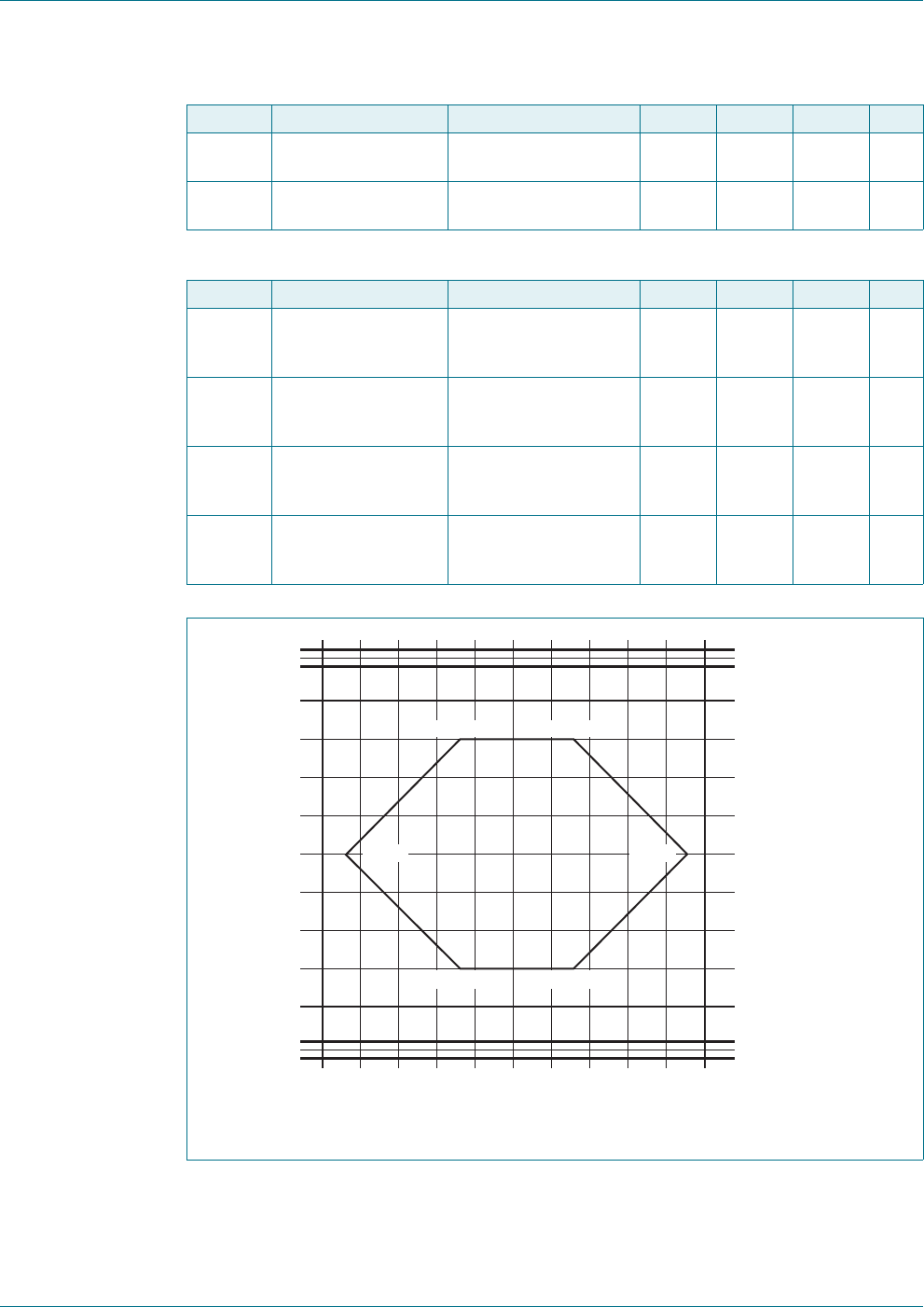
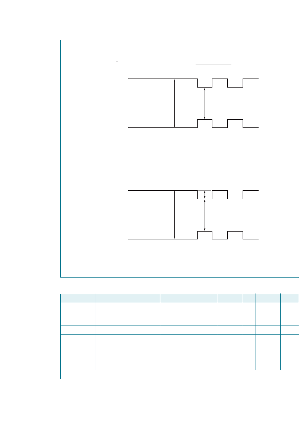
Fig 5. RX input parameters
Table 30. Input pin characteristics for RX
Symbol Parameter Conditions Min Typ Max Unit
Viinput voltage dynamic; signal
frequency at
13.56 MHz
0.7 VDDA +1 V
Ciinput capacitance 6 10 14 pF
Rsseries resistance RX input;
VDDA =3V;
receiver active;
VRX(p-p) =1V;
1.5 V DC offset
315 350 385
Minimum dynamic input voltage
VMID
A
VDD +1 V
V
in, RX
0 V
V
RX, IV, mil
m
RXmil
= V
RX, IV, mil
- V
mod
V
RX, IV, mil
+ V
mod
V
mod
13.56 MHz
carrier
Miller coded signals
aaa-002342
VMID
A
VDD +1 V
V
in, RX
0 V
V
RX, IV, Man
V
mod
V
RXMod, Man
13.56 MHz
carrier
Manchester coded signals
PR533_SDS All information provided in this document is subject to legal disclaimers. © NXP Semiconductors N.V. 2014. All rights reserved.
Product short data sheet
COMPANY PUBLIC
Rev. 3.6 — 27 October 2014
206436 24 of 36
NXP Semiconductors PR533
USB NFC integrated reader solution
[1] The minimum modulation voltage is valid for all modulation schemes except Miller coded signals.
10.20 Output pin characteristics for AUX1/AUX2
VRX(p-p) peak-to-peak receiver
voltage
Miller coded;
106 kbit/s
-150500mV
Manchester
coded; 212 kbit/s
and 424 kbit/s
-100200mV
Maximum dynamic input voltage
VRX(p-p) peak-to-peak receiver
voltage
Miller coded;
106 kbit/s
VDDA -- V
Manchester
coded;
212 and 424 kbit/s
VDDA -- V
Minimum modulation voltage
Vmod modulation voltage RxGain = 6 and 7 [1] --6mV
RxGain = 4 and 5 [1] --18mV
RxGain = 0 to 3 [1] --120mV
Minimum modulation index
m modulation index Miller coded;
106 kbit/s
VRX(p-p)=1.5V;
SensMiller = 3
-33-%
Table 30. Input pin characteristics for RX …continued
Symbol Parameter Conditions Min Typ Max Unit
Table 31. Output pin characteristics for AUX1/AUX2
Symbol Parameter Conditions Min Typ Max Unit
VOH HIGH-level output voltage VDDD =3V;
IOH =4mA
VDDD 0.4 - VDDD V
VOL LOW-level output voltage VDDD =3V;
IOL =4mA
VSSD -V
SSD +0.4 V
IOH HIGH-level output current VDDD= 3 V; VOH =
VDDD 0.3
4-- mA
IOL LOW-level output current VDDD= 3 V; VOL =
VDDD -0.3
4--mA
ILI input leakage current RSTPD_N = 0 V 1-+1A
Ciinput capacitance - 2.5 - pF
CLload capacitance - - 15 pF
PR533_SDS All information provided in this document is subject to legal disclaimers. © NXP Semiconductors N.V. 2014. All rights reserved.
Product short data sheet
COMPANY PUBLIC
Rev. 3.6 — 27 October 2014
206436 25 of 36
NXP Semiconductors PR533
USB NFC integrated reader solution
10.21 Output pin characteristics for TX1/TX2
Table 32. Output pin characteristics for TX1/TX2
Symbol Parameter Conditions Min Typ Max Unit
VOH HIGH-level output voltage VDD(TVDD) = 3 V;
IO= 32 mA; CWGsN = Fh
- - 150 mV
VDD(TVDD) = 3 V;
IO= 80 mA; CWGsN = Fh
- - 400 mV
VOL LOW-level output voltage VDD(TVDD) = 2.5 V;
IO= 32 mA; CWGsN = Fh
- - 240 mV
VDD(TVDD) = 2.5 V;
IO= 80 mA; CWGsN = Fh
- - 640 mV
Table 33. Output resistance for TX1/TX2
Symbol Parameter Conditions1 CWGsP Min Typ Max Unit
ROH HIGH-level out-
put resistance
VDD(TVDD) = 3 V; VO =
VDD(TVDD) 100 mV
01h 133 180 251
02h 67 90 125
04h 34 46 62
08h 17 23 31
10h 8.5 12 15.5
20h 4.7 6 7.8
3Fh 2.3 3 4.4
ROL LOW-level output
resistance
10h 34 46 62
20h 17 23 31
40h 8.5 12 15.5
80h 4.7 6 7.8
F0h 2.3 3 4.4
PR533_SDS All information provided in this document is subject to legal disclaimers. © NXP Semiconductors N.V. 2014. All rights reserved.
Product short data sheet
COMPANY PUBLIC
Rev. 3.6 — 27 October 2014
206436 26 of 36
NXP Semiconductors PR533
USB NFC integrated reader solution
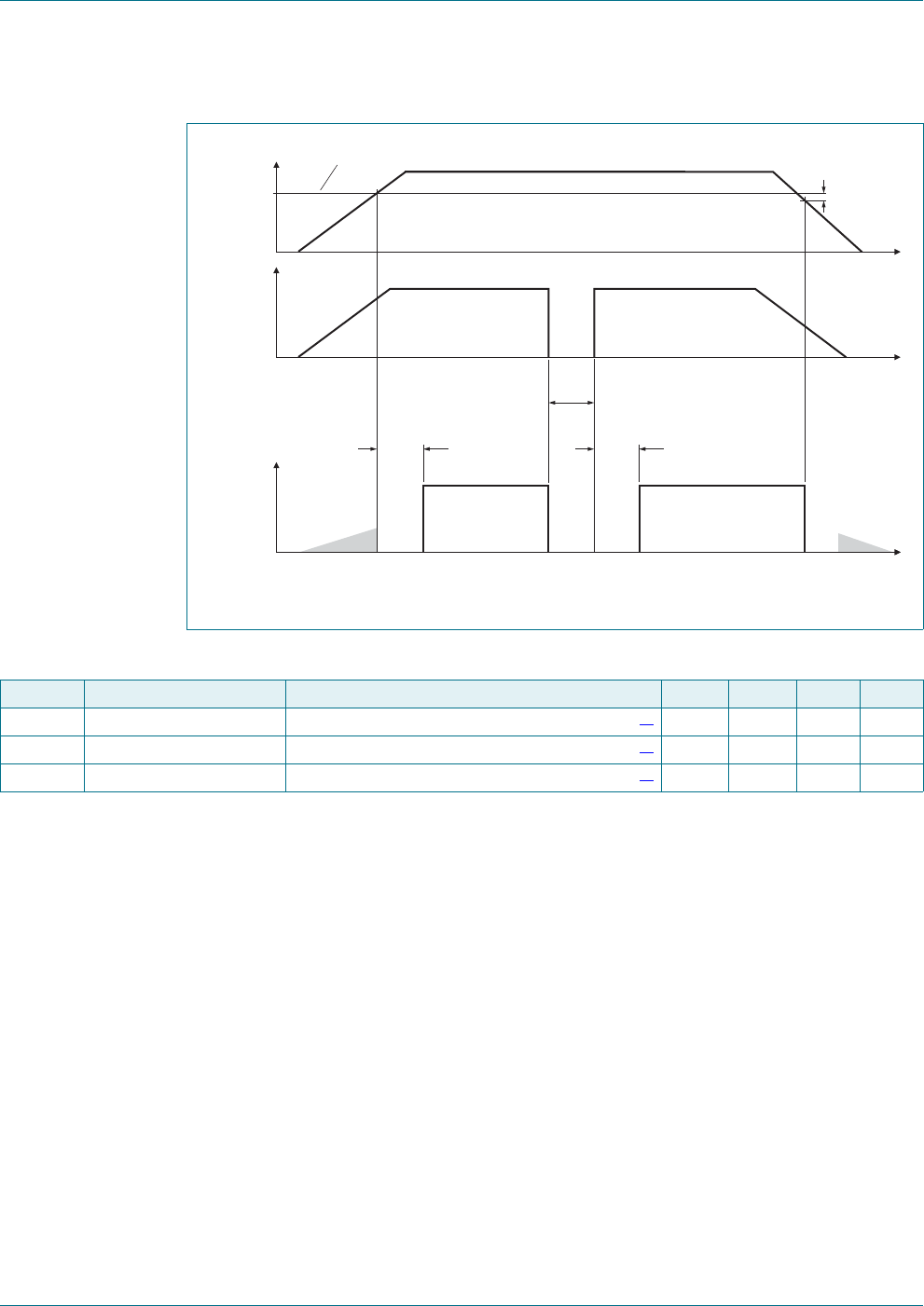
10.22 System reset timing
[1] Dependent on the 27.12 MHz crystal oscillator startup time.
[2] If the trst pulse is shorter than 20 ns, the device may be only partially reset.
Fig 6. System reset overview
t
w(rst)
t
rst
V
th(rst)reg +
V
th(rst)reg(hys)
V
th(rst)reg(hys)
V
DD(PVDD)
RSTPD_N
RSTOUT_N
t
POR
001aao394
Table 34. Reset duration time
Symbol Parameter Conditions Min Typ Max Unit
tPOR power-on reset time [1] 0.1 0.4 2 ms
trst reset time hard power-down time; user dependent [2] 20 - - ns
tw(rst) reset pulse width reset time when RSTPD_N is released [1] 0.1 0.4 2 ms
PR533_SDS All information provided in this document is subject to legal disclaimers. © NXP Semiconductors N.V. 2014. All rights reserved.
Product short data sheet
COMPANY PUBLIC
Rev. 3.6 — 27 October 2014
206436 27 of 36
NXP Semiconductors PR533
USB NFC integrated reader solution
10.23 Timing for the I2C-bus interface
[1] The PR533 has a slope control according to the I2C-bus specification for the Fast mode. The slope control
is always present and not dependent of the I2C-bus speed.
[2] 27.12 MHz quartz starts in less than 800 s. For example, quartz like TAS-3225A, TAS-7 or KSS2F with
appropriate layout.
[3] The PR533 has an internal hold time of around 270 ns for the SDA signal to bridge the undefined region of
the falling edge of P50_SCL.
Fig 7. I2C-bus parameters
Table 35. I2C-bus timing specification
Symbol Parameter Conditions Min Typ Max Unit
fSCL SCL clock frequency 0 - 400 kHz
tHD;STA hold time (repeated) START condi-
tion
after this period, the
first clock pulse is
generated
600 - - ns
tSU;STA set-up time for a repeated START
condition
600 - - ns
tSU;STO set-up time for STOP condition 600 - - ns
tLOW LOW period of the SCL clock P50_SCL 1300 - - ns
tHIGH HIGH period of the SCL clock P50_SCL 600 - - ns
tHD;DAT data hold time 0 - 900 ns
tSU;DAT data set-up time 100 - - ns
trrise time of both SDA and SCL sig-
nals
P50_SCL [1] 20 - 300 ns
tffall time of both SDA and SCL sig-
nals
P50_SCL [1] 20 - 300 ns
tBUF bus free time between a STOP
and START condition
1.3 - - ms
tstretch stretch time stretching time on
P50_SCL when
woken-up on its
own address
[2] --1ms
thhold time internal for SDA 330 - 590 ns
internal for SDA in
SPD mode
[3] -270-ns
001aaj635
SDA
tf
SCL
tLOW tf
tSP tr
tHD;STA tHD;DAT
tHD;STA
trtHIGH
tSU;DAT
SSrPS
tSU;STA
tSU;STO
tBUF

PR533_SDS All information provided in this document is subject to legal disclaimers. © NXP Semiconductors N.V. 2014. All rights reserved.
Product short data sheet
COMPANY PUBLIC
Rev. 3.6 — 27 October 2014
206436 28 of 36
NXP Semiconductors PR533
USB NFC integrated reader solution
10.24 Temperature sensor
[1] The temperature sensor embedded in the PR533 is not intended to monitor the temperature. Its purpose is
to prevent destruction of the IC due to excessive heat. The external application should include circuitry to
ensure that the ambient temperature does not exceed 85 C as specified in Table 5 “Operating conditions”.
Table 36. Temperature sensor characteristics
Symbol Parameter Conditions Min Typ Max Unit
Tth(act)otp overtemperature protection acti-
vation threshold temperature
CIU [1] 100 125 140 C
PR533_SDS All information provided in this document is subject to legal disclaimers. © NXP Semiconductors N.V. 2014. All rights reserved.
Product short data sheet
COMPANY PUBLIC
Rev. 3.6 — 27 October 2014
206436 29 of 36
NXP Semiconductors PR533
USB NFC integrated reader solution
11. Application information
12. Abbreviations
Fig 8. Application diagram of PR533
aaa-000042
RSCL
R1
L0
L0
C1
C1
C0C2
C0C2
RQ
RQ
R2
CRX
antenna
CVMID
interface supply
supply
RSDA
l2C
MEMORY
SECURE
CORE
SDA
SVDD
SIGOUT
SIGIN
TVDDP70_IRQ
RTSPD_N
PVDD
DVDD
VBUS
HOST - PROCESSOR
host interface
AVDD
OSCIN OSCOUT
AVSSDVSS
27.12 MHz
P34
RX
VMID
PR533
TX1
TVSS1
TVSS2
TX2
P50_SCL
Table 37. Abbreviations
Acronym Description
CDM Charge device Body Model
CRC Cyclic Redundancy Check
EEPROM Electrically Erasable Programmable Read-Only Memory
HBM Human Body Model
HPD Hard Power Down
MM Machine Model
NFC Near Field Communication
SPD Soft Power Down mode
PR533_SDS All information provided in this document is subject to legal disclaimers. © NXP Semiconductors N.V. 2014. All rights reserved.
Product short data sheet
COMPANY PUBLIC
Rev. 3.6 — 27 October 2014
206436 30 of 36
NXP Semiconductors PR533
USB NFC integrated reader solution
13. Revision history
[1] Revision 3.4 is not available.
Table 38. Revision history
Document ID Release date Data sheet status Change notice Supersedes
PR533_SDS v.3.6 20141027 Product short data sheet - PR533_SDS v.3.5
Modifications: •Section 1.2 “Interfaces”: updated
PR533_SDS v.3.5[1] 20141003 Product short data sheet - PR533_SDS v.3.4
Modifications: •Template updated.
•Descriptive title updated.
•Alternative descriptive title updated.
PR533_SDS v.3.3 20121020 Product short data sheet - PR533_SDS v.3.2
Modifications: •Section 14.4 “Licenses”: updated
PR533_SDS v.3.2 20120306 Product short data sheet - PR5331C3HN_SDS v.3.0
Modifications: •Section 4 “Ordering information”: updated
•General update to comply full data sheet
PR5331C3HN_SDS v.3.0 20110803 Product short data sheet - -

PR533_SDS All information provided in this document is subject to legal disclaimers. © NXP Semiconductors N.V. 2014. All rights reserved.
Product short data sheet
COMPANY PUBLIC
Rev. 3.6 — 27 October 2014
206436 31 of 36
NXP Semiconductors PR533
USB NFC integrated reader solution
14. Legal information
14.1 Data sheet status
[1] Please consult the most recently issued document before initiating or completing a design.
[2] The term ‘short data sheet’ is explained in section “Definitions”.
[3] The product status of device(s) described in this document may have changed since this document was published and may differ in case of multiple devices. The latest product status
information is available on the Internet at URL http://www.nxp.com.
14.2 Definitions
Draft — The document is a draft version only. The content is still under
internal review and subject to formal approval, which may result in
modifications or additions. NXP Semiconductors does not give any
representations or warranties as to the accuracy or completeness of
information included herein and shall have no liability for the consequences of
use of such information.
Short data sheet — A short data sheet is an extract from a full data sheet
with the same product type number(s) and title. A short data sheet is intended
for quick reference only and should not be relied upon to contain detailed and
full information. For detailed and full information see the relevant full data
sheet, which is available on request via the local NXP Semiconductors sales
office. In case of any inconsistency or conflict with the short data sheet, the
full data sheet shall prevail.
Product specification — The information and data provided in a Product
data sheet shall define the specification of the product as agreed between
NXP Semiconductors and its customer, unless NXP Semiconductors and
customer have explicitly agreed otherwise in writing. In no event however,
shall an agreement be valid in which the NXP Semiconductors product is
deemed to offer functions and qualities beyond those described in the
Product data sheet.
14.3 Disclaimers
Limited warranty and liability — Information in this document is believed to
be accurate and reliable. However, NXP Semiconductors does not give any
representations or warranties, expressed or implied, as to the accuracy or
completeness of such information and shall have no liability for the
consequences of use of such information. NXP Semiconductors takes no
responsibility for the content in this document if provided by an information
source outside of NXP Semiconductors.
In no event shall NXP Semiconductors be liable for any indirect, incidental,
punitive, special or consequential damages (including - without limitation - lost
profits, lost savings, business interruption, costs related to the removal or
replacement of any products or rework charges) whether or not such
damages are based on tort (including negligence), warranty, breach of
contract or any other legal theory.
Notwithstanding any damages that customer might incur for any reason
whatsoever, NXP Semiconductors’ aggregate and cumulative liability towards
customer for the products described herein shall be limited in accordance
with the Terms and conditions of commercial sale of NXP Semiconductors.
Right to make changes — NXP Semiconductors reserves the right to make
changes to information published in this document, including without
limitation specifications and product descriptions, at any time and without
notice. This document supersedes and replaces all information supplied prior
to the publication hereof.
Suitability for use — NXP Semiconductors products are not designed,
authorized or warranted to be suitable for use in life support, life-critical or
safety-critical systems or equipment, nor in applications where failure or
malfunction of an NXP Semiconductors product can reasonably be expected
to result in personal injury, death or severe property or environmental
damage. NXP Semiconductors and its suppliers accept no liability for
inclusion and/or use of NXP Semiconductors products in such equipment or
applications and therefore such inclusion and/or use is at the customer’s own
risk.
Applications — Applications that are described herein for any of these
products are for illustrative purposes only. NXP Semiconductors makes no
representation or warranty that such applications will be suitable for the
specified use without further testing or modification.
Customers are responsible for the design and operation of their applications
and products using NXP Semiconductors products, and NXP Semiconductors
accepts no liability for any assistance with applications or customer product
design. It is customer’s sole responsibility to determine whether the NXP
Semiconductors product is suitable and fit for the customer’s applications and
products planned, as well as for the planned application and use of
customer’s third party customer(s). Customers should provide appropriate
design and operating safeguards to minimize the risks associated with their
applications and products.
NXP Semiconductors does not accept any liability related to any default,
damage, costs or problem which is based on any weakness or default in the
customer’s applications or products, or the application or use by customer’s
third party customer(s). Customer is responsible for doing all necessary
testing for the customer’s applications and products using NXP
Semiconductors products in order to avoid a default of the applications and
the products or of the application or use by customer’s third party
customer(s). NXP does not accept any liability in this respect.
Limiting values — Stress above one or more limiting values (as defined in
the Absolute Maximum Ratings System of IEC 60134) will cause permanent
damage to the device. Limiting values are stress ratings only and (proper)
operation of the device at these or any other conditions above those given in
the Recommended operating conditions section (if present) or the
Characteristics sections of this document is not warranted. Constant or
repeated exposure to limiting values will permanently and irreversibly affect
the quality and reliability of the device.
Terms and conditions of commercial sale — NXP Semiconductors
products are sold subject to the general terms and conditions of commercial
sale, as published at http://www.nxp.com/profile/terms, unless otherwise
agreed in a valid written individual agreement. In case an individual
agreement is concluded only the terms and conditions of the respective
agreement shall apply. NXP Semiconductors hereby expressly objects to
applying the customer’s general terms and conditions with regard to the
purchase of NXP Semiconductors products by customer.
No offer to sell or license — Nothing in this document may be interpreted or
construed as an offer to sell products that is open for acceptance or the grant,
conveyance or implication of any license under any copyrights, patents or
other industrial or intellectual property rights.
Document status[1][2] Product status[3] Definition
Objective [short] data sheet Development This document contains data from the objective specification for product development.
Preliminary [short] data sheet Qualification This document contains data from the preliminary specification.
Product [short] data sheet Production This document contains the product specification.

PR533_SDS All information provided in this document is subject to legal disclaimers. © NXP Semiconductors N.V. 2014. All rights reserved.
Product short data sheet
COMPANY PUBLIC
Rev. 3.6 — 27 October 2014
206436 32 of 36
NXP Semiconductors PR533
USB NFC integrated reader solution
Export control — This document as well as the item(s) described herein
may be subject to export control regulations. Export might require a prior
authorization from competent authorities.
Quick reference data — The Quick reference data is an extract of the
product data given in the Limiting values and Characteristics sections of this
document, and as such is not complete, exhaustive or legally binding.
Non-automotive qualified products — Unless this data sheet expressly
states that this specific NXP Semiconductors product is automotive qualified,
the product is not suitable for automotive use. It is neither qualified nor tested
in accordance with automotive testing or application requirements. NXP
Semiconductors accepts no liability for inclusion and/or use of
non-automotive qualified products in automotive equipment or applications.
In the event that customer uses the product for design-in and use in
automotive applications to automotive specifications and standards, customer
(a) shall use the product without NXP Semiconductors’ warranty of the
product for such automotive applications, use and specifications, and (b)
whenever customer uses the product for automotive applications beyond
NXP Semiconductors’ specifications such use shall be solely at customer’s
own risk, and (c) customer fully indemnifies NXP Semiconductors for any
liability, damages or failed product claims resulting from customer design and
use of the product for automotive applications beyond NXP Semiconductors’
standard warranty and NXP Semiconductors’ product specifications.
Translations — A non-English (translated) version of a document is for
reference only. The English version shall prevail in case of any discrepancy
between the translated and English versions.
14.4 Licenses
14.5 Trademarks
Notice: All referenced brands, product names, service names and trademarks
are the property of their respective owners.
MIFARE — is a trademark of NXP Semiconductors N.V.
I2C-bus — logo is a trademark of NXP Semiconductors N.V.
15. Contact information
For more information, please visit: http://www.nxp.com
For sales office addresses, please send an email to: salesaddresses@nxp.com
Purchase of NXP ICs with ISO/IEC 14443 type B functionality
This NXP Semiconductors IC is ISO/IEC 14443 Type B
software enabled and is licensed under Innovatron’s
Contactless Card patents license for ISO/IEC 14443 B.
The license includes the right to use the IC in systems
and/or end-user equipment.
RATP/Innovatron
Technology
Purchase of NXP ICs with NFC technology
Purchase of an NXP Semiconductors IC that complies with one of the Near
Field Communication (NFC) standards ISO/IEC 18092 and ISO/IEC 21481
does not convey an implied license under any patent right infringed by
implementation of any of those standards.

PR533_SDS All information provided in this document is subject to legal disclaimers. © NXP Semiconductors N.V. 2014. All rights reserved.
Product short data sheet
COMPANY PUBLIC
Rev. 3.6 — 27 October 2014
206436 33 of 36
NXP Semiconductors PR533
USB NFC integrated reader solution
Notes

PR533_SDS All information provided in this document is subject to legal disclaimers. © NXP Semiconductors N.V. 2014. All rights reserved.
Product short data sheet
COMPANY PUBLIC
Rev. 3.6 — 27 October 2014
206436 34 of 36
NXP Semiconductors PR533
USB NFC integrated reader solution
16. Tables
Table 1. Quick reference data . . . . . . . . . . . . . . . . . . . . .3
Table 2. Ordering information . . . . . . . . . . . . . . . . . . . . .4
Table 3. PR533 pin description . . . . . . . . . . . . . . . . . . . .5
Table 4. Limiting values . . . . . . . . . . . . . . . . . . . . . . . . . .7
Table 5. Operating conditions . . . . . . . . . . . . . . . . . . . . .8
Table 6. Thermal characteristics . . . . . . . . . . . . . . . . . . .8
Table 7. Current consumption characteristics . . . . . . . . .9
Table 8. Voltage regulator characteristics[1] . . . . . . . . . . .9
Table 9. Antenna presence detection. . . . . . . . . . . . . . .10
Table 10. Crystal requirements. . . . . . . . . . . . . . . . . . . . . 11
Table 11. Pin characteristics for 27.12 MHz XTAL
Oscillator (OSCIN, OSCOUT). . . . . . . . . . . . . . 11
Table 12. RSTPD_N input pin characteristics . . . . . . . . .12
Table 13. Input pin characteristics for I0, I1 and
TESTEN . . . . . . . . . . . . . . . . . . . . . . . . . . . . .12
Table 14. RSTOUT_N output pin characteristics . . . . . . .13
Table 15. Input/output pin characteristics for
pin P70_IRQ . . . . . . . . . . . . . . . . . . . . . . . . . . .14
Table 16. Input/output pin characteristics for P30 /
UART_RX, P31 / UART_TX, P32_INT0,
P33_INT1 . . . . . . . . . . . . . . . . . . . . . . . . . . . . .15
Table 17. Input/output pin characteristics for P35 . . . . . .16
Table 18. Input/output pin characteristics for DP
and DM for USB interface. . . . . . . . . . . . . . . . .17
Table 19. USB DP/DM differential receiver input levels . .18
Table 20. USB DP/DM driver characteristics . . . . . . . . . .18
Table 21. Input Pin characteristics for DP for HSU
interface . . . . . . . . . . . . . . . . . . . . . . . . . . . . . .19
Table 22. Output Pin characteristics for DM for HSU
interface . . . . . . . . . . . . . . . . . . . . . . . . . . . . . .19
Table 23. Input/output drain output pin characteristics
for SCL I2C interface. . . . . . . . . . . . . . . . . . . . .20
Table 24. Input/output drain output pin characteristics
for SDA I2C interface . . . . . . . . . . . . . . . . . . . .20
Table 25. Output pin characteristics for DELATT . . . . . . .21
Table 26. Input/output pin characteristics for SIGIN. . . . .21
Table 27. Output pin characteristics for SIGOUT . . . . . . .21
Table 28. Input/output pin characteristics for P34 . . . . . .22
Table 29. Output pin characteristics for LOADMOD . . . .22
Table 30. Input pin characteristics for RX . . . . . . . . . . . .23
Table 31. Output pin characteristics for AUX1/AUX2 . . .24
Table 32. Output pin characteristics for TX1/TX2. . . . . . .25
Table 33. Output resistance for TX1/TX2 . . . . . . . . . . . . .25
Table 34. Reset duration time . . . . . . . . . . . . . . . . . . . . .26
Table 35. I2C-bus timing specification . . . . . . . . . . . . . . .27
Table 36. Temperature sensor characteristics . . . . . . . . .28
Table 37. Abbreviations . . . . . . . . . . . . . . . . . . . . . . . . . .29
Table 38. Revision history . . . . . . . . . . . . . . . . . . . . . . . .30

PR533_SDS All information provided in this document is subject to legal disclaimers. © NXP Semiconductors N.V. 2014. All rights reserved.
Product short data sheet
COMPANY PUBLIC
Rev. 3.6 — 27 October 2014
206436 35 of 36
NXP Semiconductors PR533
USB NFC integrated reader solution
17. Figures
Fig 1. Block diagram . . . . . . . . . . . . . . . . . . . . . . . . . . . .4
Fig 2. Pin configuration for HVQFN 40 (SOT618-1) . . . .5
Fig 3. 27.12 MHz input clock phase noise spectrum
mask . . . . . . . . . . . . . . . . . . . . . . . . . . . . . . . . . .11
Fig 4. Transmit waveform at DP/DM . . . . . . . . . . . . . . .18
Fig 5. RX input parameters . . . . . . . . . . . . . . . . . . . . . .23
Fig 6. System reset overview. . . . . . . . . . . . . . . . . . . . .26
Fig 7. I2C-bus parameters . . . . . . . . . . . . . . . . . . . . . . .27
Fig 8. Application diagram of PR533 . . . . . . . . . . . . . . .29

NXP Semiconductors PR533
USB NFC integrated reader solution
© NXP Semiconductors N.V. 2014. All rights reserved.
For more information, please visit: http://www.nxp.com
For sales office addresses, please send an email to: salesaddresses@nxp.com
Date of release: 27 October 2014
206436
Please be aware that important notices concerning this document and the product(s)
described herein, have been included in section ‘Legal information’.
18. Contents
1 General description . . . . . . . . . . . . . . . . . . . . . . 1
1.1 RF protocols . . . . . . . . . . . . . . . . . . . . . . . . . . . 1
1.2 Interfaces . . . . . . . . . . . . . . . . . . . . . . . . . . . . . 1
1.3 Standards compliancy. . . . . . . . . . . . . . . . . . . . 1
1.4 Supported operating systems . . . . . . . . . . . . . . 2
2 Features and benefits . . . . . . . . . . . . . . . . . . . . 2
3 Quick reference data . . . . . . . . . . . . . . . . . . . . . 3
4 Ordering information. . . . . . . . . . . . . . . . . . . . . 4
5 Block diagram . . . . . . . . . . . . . . . . . . . . . . . . . . 4
6 Pinning information. . . . . . . . . . . . . . . . . . . . . . 5
6.1 Pinning . . . . . . . . . . . . . . . . . . . . . . . . . . . . . . . 5
6.2 Pin description . . . . . . . . . . . . . . . . . . . . . . . . . 5
7 Limiting values. . . . . . . . . . . . . . . . . . . . . . . . . . 7
8 Recommended operating conditions. . . . . . . . 8
9 Thermal characteristics . . . . . . . . . . . . . . . . . . 8
10 Characteristics. . . . . . . . . . . . . . . . . . . . . . . . . . 8
10.1 Power management characteristics . . . . . . . . . 8
10.1.1 Current consumption characteristics . . . . . . . . 8
10.1.2 Voltage regulator characteristics. . . . . . . . . . . . 9
10.2 Antenna presence self test thresholds . . . . . . . 9
10.3 Typical 27.12 MHz Crystal requirements . . . . 11
10.4 Pin characteristics for 27.12 MHz XTAL
Oscillator (OSCIN, OSCOUT). . . . . . . . . . . . . 11
10.5 RSTPD_N input pin characteristics . . . . . . . . 12
10.6 Input pin characteristics for I0, I1 and
TESTEN . . . . . . . . . . . . . . . . . . . . . . . . . . . . . 12
10.7 RSTOUT_N output pin characteristics . . . . . . 13
10.8 Input/output characteristics for pin P70_IRQ . 14
10.9 Input/output pin characteristics for P30 /
UART_RX, P31 / UART_TX, P32_INT0,
P33_INT1 . . . . . . . . . . . . . . . . . . . . . . . . . . . . 15
10.10 Input/output pin characteristics for P35 . . . . . 16
10.11 Input/output pin characteristics for DP and DM 17
10.12 Input pin characteristics for SCL. . . . . . . . . . . 20
10.13 Input/output pin characteristics for SDA . . . . . 20
10.14 Output pin characteristics for DELATT . . . . . . 21
10.15 Input pin characteristics for SIGIN . . . . . . . . . 21
10.16 Output pin characteristics for SIGOUT . . . . . . 21
10.17 Input/output pin characteristics for P34 . . . . . 22
10.18 Output pin characteristics for LOADMOD. . . . 22
10.19 Input pin characteristics for RX. . . . . . . . . . . . 23
10.20 Output pin characteristics for AUX1/AUX2 . . . 24
10.21 Output pin characteristics for TX1/TX2. . . . . . 25
10.22 System reset timing . . . . . . . . . . . . . . . . . . . . 26
10.23 Timing for the I2C-bus interface . . . . . . . . . . . 27
10.24 Temperature sensor . . . . . . . . . . . . . . . . . . . . 28
11 Application information . . . . . . . . . . . . . . . . . 29
12 Abbreviations . . . . . . . . . . . . . . . . . . . . . . . . . 29
13 Revision history . . . . . . . . . . . . . . . . . . . . . . . 30
14 Legal information . . . . . . . . . . . . . . . . . . . . . . 31
14.1 Data sheet status . . . . . . . . . . . . . . . . . . . . . . 31
14.2 Definitions . . . . . . . . . . . . . . . . . . . . . . . . . . . 31
14.3 Disclaimers . . . . . . . . . . . . . . . . . . . . . . . . . . 31
14.4 Licenses. . . . . . . . . . . . . . . . . . . . . . . . . . . . . 32
14.5 Trademarks . . . . . . . . . . . . . . . . . . . . . . . . . . 32
15 Contact information . . . . . . . . . . . . . . . . . . . . 32
16 Tables . . . . . . . . . . . . . . . . . . . . . . . . . . . . . . . . 34
17 Figures . . . . . . . . . . . . . . . . . . . . . . . . . . . . . . . 35
18 Contents. . . . . . . . . . . . . . . . . . . . . . . . . . . . . . 36