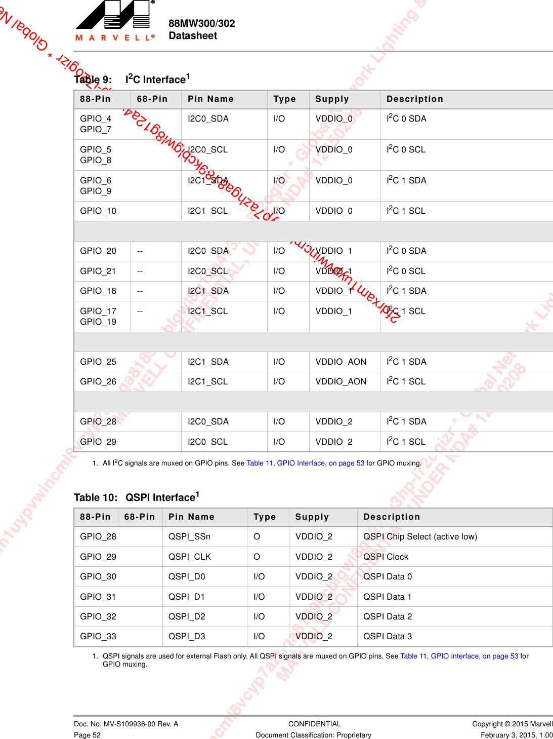
Globalscale Technologies GTIMW302 GTI MW302 Module User Manual 88MW300 302 Datasheet
Globalscale Technologies INC GTI MW302 Module 88MW300 302 Datasheet
UserManual.wiki
>
Globalscale Technologies
>
GTIMW302 User Manual
User manual
Navigation menu
Upload a User Manual
Namespaces
Wiki Guide
HTML
PDF
Info
Views
User Manual
Discussion / Help
Navigation
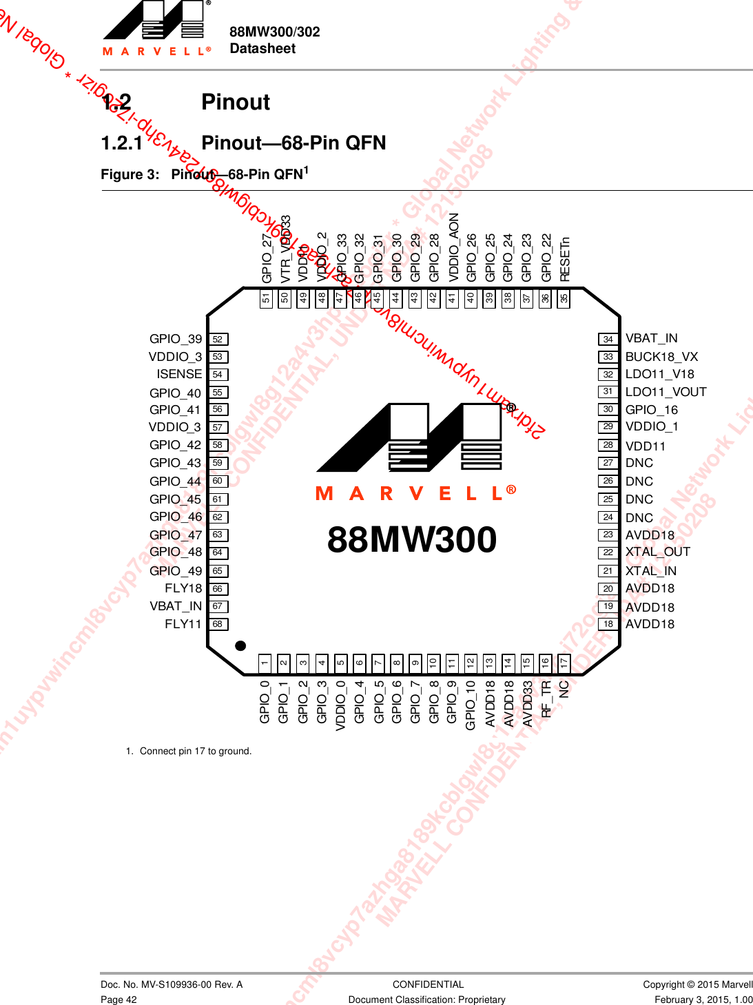
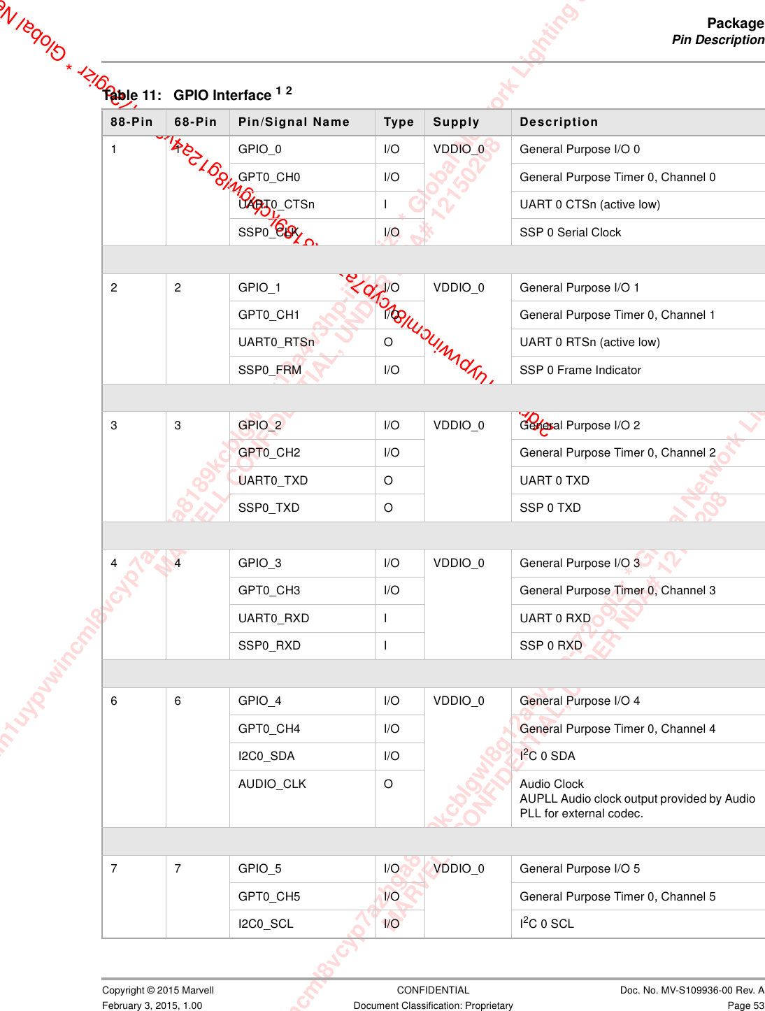
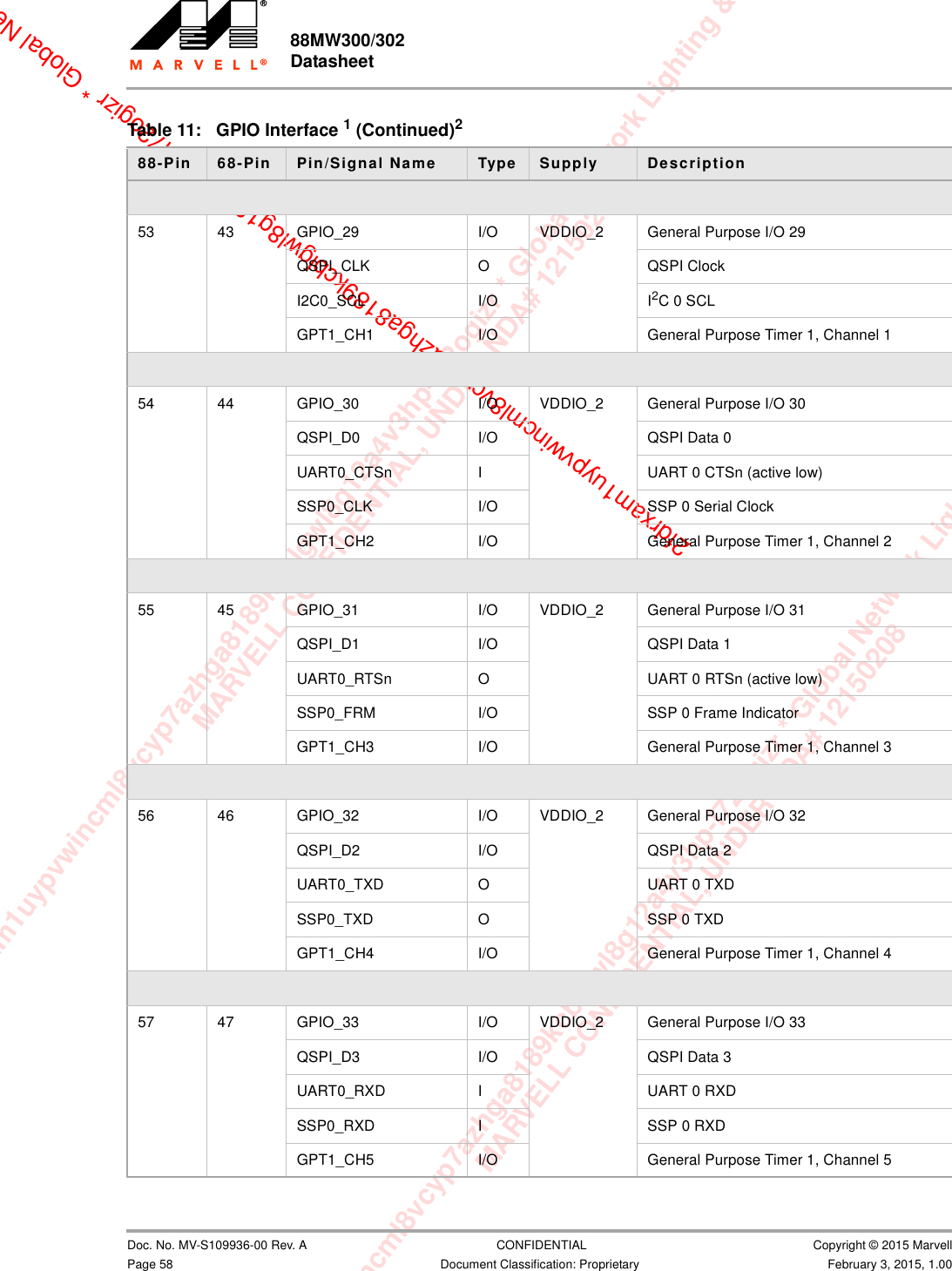
![xam1uypvwincml8vcyp7azhga8189kcblgwl8g12a4v3hp-i72ogizr * Global Network Lighting & ConMARVELL CONFIDENTIAL, UNDER NDA# 12150208m1uypvwincml8vcyp7azhga8189kcblgwl8g12a4v3hp-i72ogizr * Global Network Lighting & Control InMARVELL CONFIDENTIAL, UNDER NDA# 121502082fdrxam1uypvwincml8vcyp7azhga8189kcblgwl8g12a4v3hp-i72ogizr * Global NetPackagePin Description Copyright © 2015 Marvell CONFIDENTIAL Doc. No. MV-S109936-00 Rev. AFebruary 3, 2015, 1.00 Document Classification: Proprietary Page 5513 -- GPIO_11 I/O VDDIO_0 General Purpose I/O 11GPT2_CH0 I/O General Purpose Timer 2, Channel 0UART1_CTSn I UART 1 CTSn (active low)SSP1_CLK I/O SSP 1 Serial Clock14 -- GPIO_12 I/O VDDIO_0 General Purpose I/O 12GPT2_CH1 I/O General Purpose Timer 2, Channel 1UART1_RTSn O UART 1 RTSn (active low)SSP1_FRM I/O SSP 1 Frame Indicator15 -- GPIO_13 I/O VDDIO_0 General Purpose I/O 13GPT2_CH2 I/O General Purpose Timer 2, Channel 2UART1_TXD O UART 1 TXDSSP1_TXD O SSP 1 TXD16 -- GPIO_14 I/O VDDIO_0 General Purpose I/O 14GPT2_CH3 I/O General Purpose Timer 2, Channel 3UART1_RXD I UART 1 RXDSSP1_RXD I SSP 1 RXD17 -- GPIO_15 I/O VDDIO_0 General Purpose I/O 15GPT2_CH4 I/O General Purpose Timer 2, Channel 435 30 GPIO_16 I/O VDDIO_1 General Purpose I/O 16CON[5] I/O Configuration BitSee Table 17, Configuration Pins, on page 67.AUDIO_CLK O Audio ClockAUPLL Audio clock output provided by Audio PLL for external codec.Table 11: GPIO Interface 1 (Continued)288-Pin 68-Pin Pin/Signal Name Type Supply Description](https://usermanual.wiki/Globalscale-Technologies/GTIMW302/User-Guide-2777835-Page-19.png)
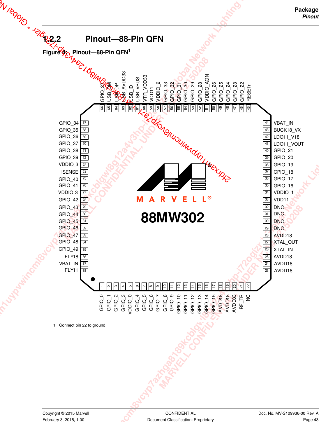
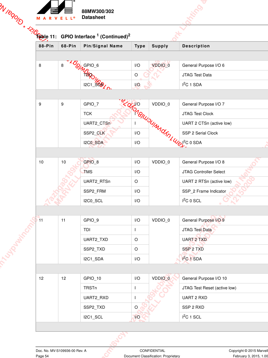
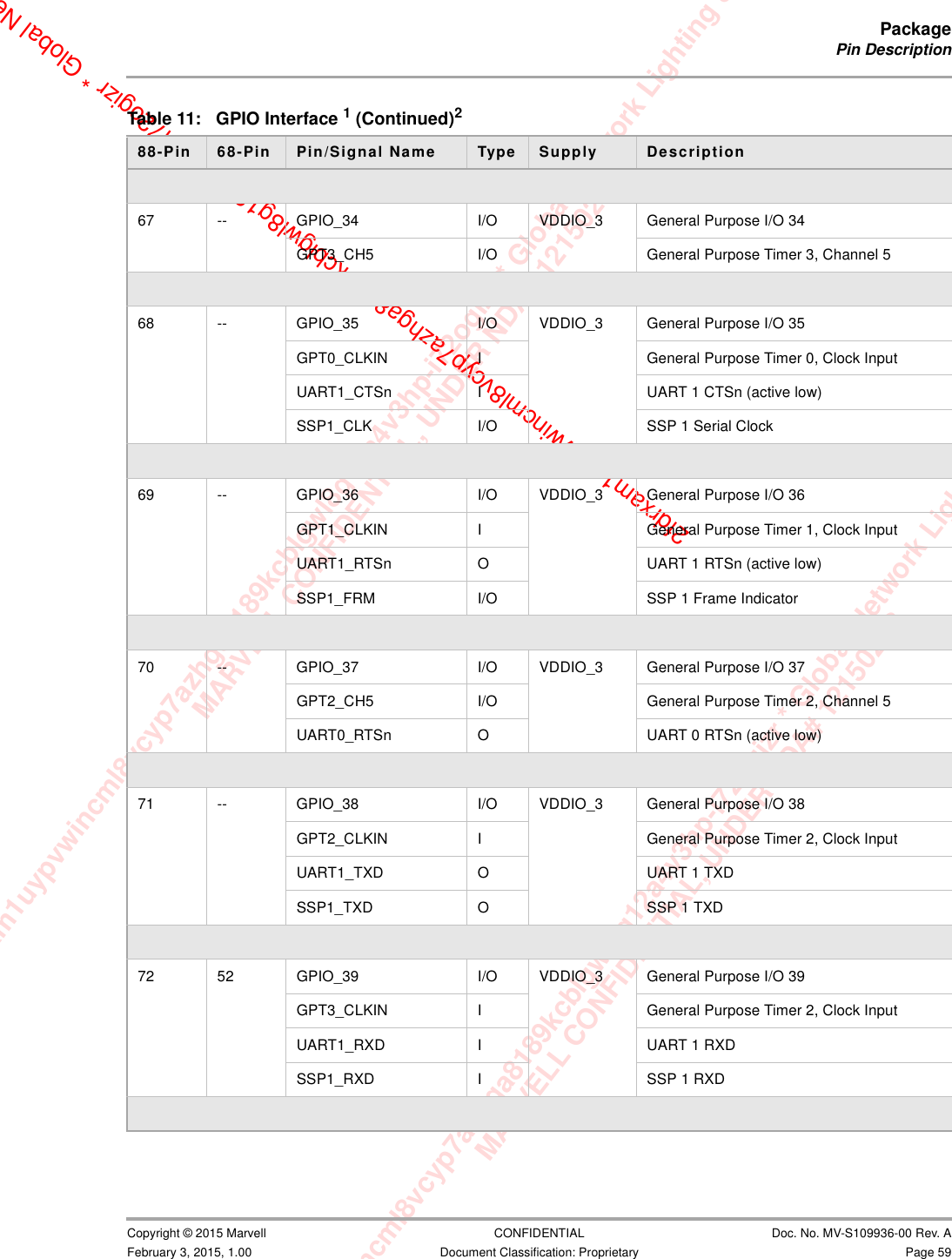
![xam1uypvwincml8vcyp7azhga8189kcblgwl8g12a4v3hp-i72ogizr * Global Network Lighting & ConMARVELL CONFIDENTIAL, UNDER NDA# 12150208m1uypvwincml8vcyp7azhga8189kcblgwl8g12a4v3hp-i72ogizr * Global Network Lighting & Control InMARVELL CONFIDENTIAL, UNDER NDA# 121502082fdrxam1uypvwincml8vcyp7azhga8189kcblgwl8g12a4v3hp-i72ogizr * Global NetPackagePin Description Copyright © 2015 Marvell CONFIDENTIAL Doc. No. MV-S109936-00 Rev. AFebruary 3, 2015, 1.00 Document Classification: Proprietary Page 5747 37 GPIO_23 I/O VDDIO_AONGeneral Purpose I/O 23UART0_CTSn I UART 0 CTSn (active low)WAKE_UP1 I Wake-Up 1COMP_IN_P I LDO18 Comparator Input, PositivePositive input to LDO18 comparator.48 38 GPIO_24 I/O VDDIO_AONGeneral Purpose I/O 24UART0_RXD I UART 0 RXDGPT1_CH5 I/O General Purpose Timer 1, Channel 5COMP_IN_N I LDO18 Comparator Input, NegativeNegative input to LDO18 comparator.49 39 GPIO_25 I/O VDDIO_AONGeneral Purpose I/O 25XTAL32K_IN I 32.768 kHz Crystal InputI2C1_SDA I/O I2C1 SDA50 40 GPIO_26 I/O VDDIO_AONGeneral Purpose I/O 26XTAL32K_OUT O 32.768 kHz Crystal OutputI2C1_SCL I/O I2C1 SCL66 51 GPIO_27 I/O VDDIO_3 General Purpose I/O 27-- USB_DRV_VBUS O Drive 5V on VBUS51 UART0_TXD O UART 0 TXD51 CON[4] I/O Configuration BitSee Table 17, Configuration Pins, on page 67.52 42 GPIO_28 I/O VDDIO_2 General Purpose I/O 28QSPI_SSn O QSPI Chip Select (active low)I2C0_SDA I/O I2C0 SDAGPT1_CH0 I/O General Purpose Timer 1, Channel 0Table 11: GPIO Interface 1 (Continued)288-Pin 68-Pin Pin/Signal Name Type Supply Description](https://usermanual.wiki/Globalscale-Technologies/GTIMW302/User-Guide-2777835-Page-21.png)
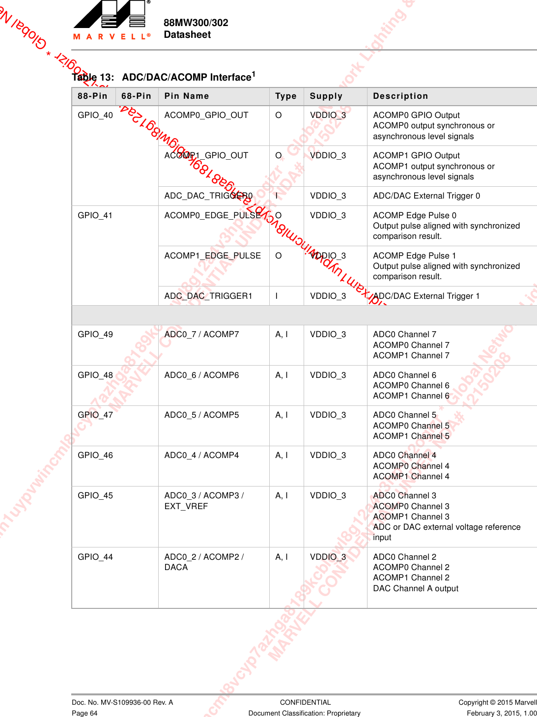
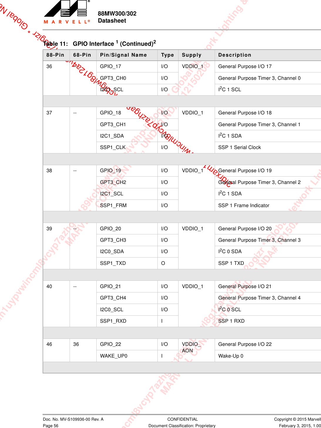
![xam1uypvwincml8vcyp7azhga8189kcblgwl8g12a4v3hp-i72ogizr * Global Network Lighting & ConMARVELL CONFIDENTIAL, UNDER NDA# 12150208m1uypvwincml8vcyp7azhga8189kcblgwl8g12a4v3hp-i72ogizr * Global Network Lighting & Control InMARVELL CONFIDENTIAL, UNDER NDA# 121502082fdrxam1uypvwincml8vcyp7azhga8189kcblgwl8g12a4v3hp-i72ogizr * Global NetPackageConfiguration Pins Copyright © 2015 Marvell CONFIDENTIAL Doc. No. MV-S109936-00 Rev. AFebruary 3, 2015, 1.00 Document Classification: Proprietary Page 671.5 Configuration PinsTable 17 shows the pins used as configuration inputs to set parameters following a reset. The definition of these pins changes immediately after reset to their usual function. To set a configuration bit to 0, attach a 100 kΩ resistor from the pin to ground. No external circuitry is required to set a configuration bit to 1. Table 17: Configuration PinsConfiguration Bits Pin Name Configuration FunctionCON[5] GPIO_16 Boot Options 00 = boot from UART01 = reserved 10 = boot from USB 11 = boot from Flash (default) CON[4] GPIO_27](https://usermanual.wiki/Globalscale-Technologies/GTIMW302/User-Guide-2777835-Page-31.png)