Globalscale Technologies GTIMW302 GTI MW302 Module User Manual 88MW300 302 Datasheet
Globalscale Technologies INC GTI MW302 Module 88MW300 302 Datasheet
User manual

xam1
uypvwincml8vcyp7azhga8189kcblgwl8g12a4v3hp-i72ogizr * Global Network Lighting &
Con
MARVELL CONFIDENTIAL, UNDER NDA# 12150208
m1u
ypvwincml8vcyp7azhga8189kcblgwl8g12a4v3hp-i72ogizr * Global Network Lighting & Con
trol In
MARVELL CONFIDENTIAL, UNDER NDA# 12150208
2fdrxam1uypvwincml8vcyp7azhga8189kcblgwl8g12a4v3hp-i72ogizr * Globa
l Net
Doc. No. MV-S109936-00, Rev. A
February 3, 2015, 1.00
CONFIDENTIAL
Document Classification: Proprietary
Cover
88MW300/302
WLAN Microcontroller
IEEE 802.11n/g/b
Datasheet

xam1
uypvwincml8vcyp7azhga8189kcblgwl8g12a4v3hp-i72ogizr * Global Network Lighting &
Con
MARVELL CONFIDENTIAL, UNDER NDA# 12150208
m1u
ypvwincml8vcyp7azhga8189kcblgwl8g12a4v3hp-i72ogizr * Global Network Lighting & Con
trol In
MARVELL CONFIDENTIAL, UNDER NDA# 12150208
2fdrxam1uypvwincml8vcyp7azhga8189kcblgwl8g12a4v3hp-i72ogizr * Globa
l Net
Document Conventions
Note: Provides related information or information of special importance.
Caution: Indicates potential damage to hardware or software, or loss of data.
Warning: Indicates a risk of personal injury.
Document Status
Doc Status: 1.00 Technical Publication: 0.xx
For more information, visit our website at: http://www.marvell.com
Disclaimer
No part of this document may be reproduced or transmitted in any form or by any means, electronic or mechanical, including photocopying and recording, for any purpose,
without the express written permission of Marvell. Marvell retains the right to make changes to this document at any time, without notice. Marvell makes no warranty of any
kind, expressed or implied, with regard to any information contained in this document, including, but not limited to, the implied warranties of merchantability or fitness for any
particular purpose. Further, Marvell does not warrant the accuracy or completeness of the information, text, graphics, or other items contained within this document.
Marvell products are not designed for use in life-support equipment or applications that would cause a life-threatening situation if any such products failed. Do not use
Marvell products in these types of equipment or applications.
With respect to the products described herein, the user or recipient, in the absence of appropriate U.S. government authorization, agrees:
1) Not to re-export or release any such information consisting of technology, software or source code controlled for national security reasons by the U.S. Export Control
Regulations ("EAR"), to a national of EAR Country Groups D:1 or E:2;
2) Not to export the direct product of such technology or such software, to EAR Country Groups D:1 or E:2, if such technology or software and direct products thereof are
controlled for national security reasons by the EAR; and,
3) In the case of technology controlled for national security reasons under the EAR where the direct product of the technology is a complete plant or component of a plant,
not to export to EAR Country Groups D:1 or E:2 the direct product of the plant or major component thereof, if such direct product is controlled for national security reasons
by the EAR, or is subject to controls under the U.S. Munitions List ("USML").
At all times hereunder, the recipient of any such information agrees that they shall be deemed to have manually signed this document in connection with their receipt of any
such information.
Copyright © 1999–2015. Marvell International Ltd. All rights reserved. Alaska, ARMADA, Avanta, Avastar, CarrierSpan, Kinoma, Link Street, LinkCrypt, Marvell logo,
Marvell, Moving Forward Faster, Marvell Smart, PISC, Prestera, Qdeo, QDEO logo, QuietVideo, Virtual Cable Tester, The World as YOU See It, Vmeta, Xelerated, and
Yukon are registered trademarks of Marvell or its affiliates. G.now, HyperDuo, Kirkwood, and Wirespeed by Design are trademarks of Marvell or its affiliates.
Patent(s) Pending—Products identified in this document may be covered by one or more Marvell patents and/or patent applications.
88MW300/302
Datasheet
Doc. No. MV-S109936-00 Rev. A CONFIDENTIAL Copyright © 2015 Marvell
Page 2 Document Classification: Proprietary February 3, 2015, 1.00

xam1
uypvwincml8vcyp7azhga8189kcblgwl8g12a4v3hp-i72ogizr * Global Network Lighting &
Con
MARVELL CONFIDENTIAL, UNDER NDA# 12150208
m1u
ypvwincml8vcyp7azhga8189kcblgwl8g12a4v3hp-i72ogizr * Global Network Lighting & Con
trol In
MARVELL CONFIDENTIAL, UNDER NDA# 12150208
2fdrxam1uypvwincml8vcyp7azhga8189kcblgwl8g12a4v3hp-i72ogizr * Globa
l Net
88MW300/302
WLAN Microcontroller
Datasheet
Copyright © 2015 Marvell CONFIDENTIAL Doc. No. MV-S109936-00 Rev. A
February 3, 2015, 1.00 Document Classification: Proprietary Page 3
PRODUCT OVERVIEW
The Marvell® 88MW300/302 is a highly integrated,
low-power WLAN Microcontroller System-on-Chip (SoC)
solution designed for a broad array of smart devices for
Internet of Things (IoT), wearables, accessories,
Machine-to-Machine (M2M), home automation, and
Smart Energy applications
A high degree of integration enables very low system
costs requiring only a single 3.3V power input, a
38.4 MHz crystal, and SPI Flash. The RF path needs
only a lowpass filter for antenna connection.
The SoC includes a full-featured W LAN subsystem
powered by proven and mature IEEE 802.11n/g/b
Marvell technology. The WLAN subsystem integrates a
WLAN MAC, baseband, and direct-conversion RF radio
with integrated PA, LNA, and transmit/receive switch. It
also integrates a CPU subsystem with integrated
memory to run Marvell WLAN firmware to handle real
time WLAN protocol processing to off-load many WLAN
functions from the main application CPU.
The 88MW300/302 application subsystem is powered by
an ARM Cortex-M4F CPU that operates up to 200 MHz.
The device supports an integrated 512 KB SRAM,
128 KB mask ROM, and a QSPI interface to external
Flash. An integrated Flash Controller with a 32 KB
SRAM cache enables eXecute In Place (XIP) support for
firmware from Flash.
The SoC is designed for low-power operation and
includes several low-power states and fast wake-up
times. Multiple power domains and clocks can be
individually shut down to save power. The SoC also has
a high-efficiency internal PA that can be operated in
low-power mode to save power. The microcontroller and
WLAN subsystems can be placed into low-power states,
independently, supporting a variety of application use
cases. An internal DC-DC regulator provides the 1.8V
rail for the WLAN subsystem.
The SoC provides a full array of peripheral interfaces
including SSP/SPI/I2S (3x), UART (3x), I2C (2x), General
Purpose Timers and PWM, ADC, DAC, Analog
Comparator, and GPIOs. It also includes a hardware
cryptographic engine, RTC, and Watchdog Timer. The
88MW302 includes a high speed USB On-The-Go
(OTG) interface to enable USB audio, video, and other
applications.
A complete set of digital and analog interfaces enable
direct interfacing for I/O avoiding the need for external
chips. The application CPU can be used to support
custom application development avoiding the need for
another microcontroller or processor.
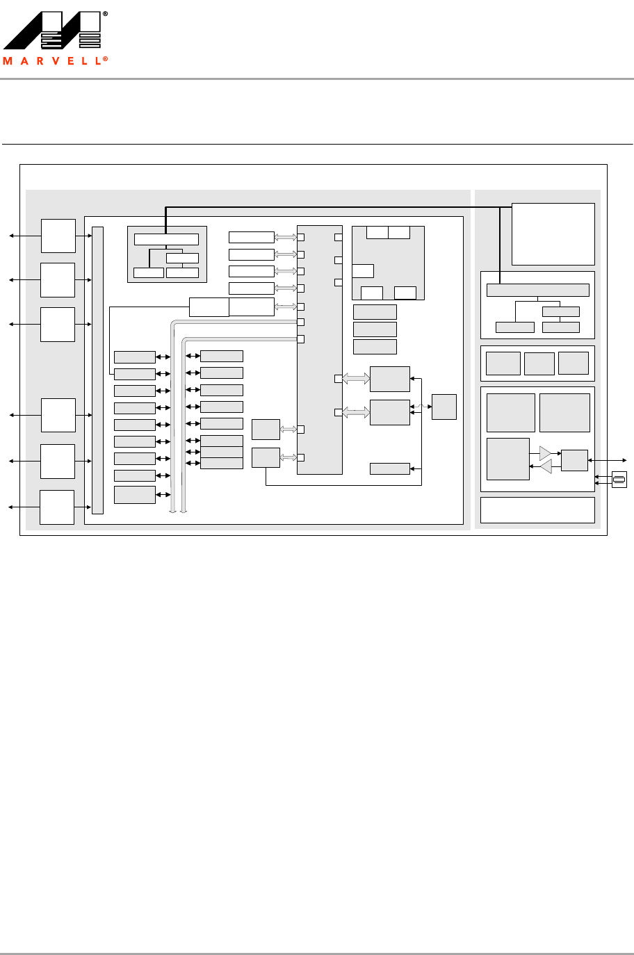
Figure 1 shows an overall block diagram of the device.
xam1
uypvwincml8vcyp7azhga8189kcblgwl8g12a4v3hp-i72ogizr * Global Network Lighting &
Con
MARVELL CONFIDENTIAL, UNDER NDA# 12150208
m1u
ypvwincml8vcyp7azhga8189kcblgwl8g12a4v3hp-i72ogizr * Global Network Lighting & Con
trol In
MARVELL CONFIDENTIAL, UNDER NDA# 12150208
2fdrxam1uypvwincml8vcyp7azhga8189kcblgwl8g12a4v3hp-i72ogizr * Globa
l Net
88MW300/302
Datasheet
Doc. No. MV-S109936-00 Rev. A CONFIDENTIAL Copyright © 2015 Marvell
Page 4 Document Classification: Proprietary February 3, 2015, 1.00
Applications
White goods/appliances—refrigerator, washer,
dryer, oven range, microwave, dishwasher, water
heater, air conditioner
Consumer devices and accessories—toys,
speakers, headset, alarm clock, gaming accessory,
remote control
Home automation—smart outlet, light switch,
security camera, thermostat, sprinkler controller,
sensor, door lock, door bell, garage door, security
system
Personal health devices—weighing scale,
glucometer, blood pressure monitor, fitness
equipment
IoT/wearables—coffee pot, rice cooker, vacuum
cleaner, air purifier, smart watch, fitness bracelet,
pet monitor
Commercial/industrial—lighting, building
automation, asset management, Point of Sale
(POS) sales
Gateways—Connecting IR, sub-Gig or Legacy RF,
Bluetooth Smart, ZigBee, ZWave and other radios to
Wi-Fi/IP network
Key Features
Highly integrated SoC requiring very few external
components for a full system operation
Multiple low-power modes and fast wake-up times
Full-featured, single stream 802.11n/g/b WLAN
High-efficiency PA with a low-power (10 dB) mode
Cortex-M4F application CPU for applications with
integrated 512 KB SRAM and 128 KB mask ROM
Flash Controller with embedded 32 KB SRAM
cache to support XIP from external SPI Flash
Secure boot
Full set of digital and analog I/O interfaces
Power Management
Power modes—active, idle, standby, sleep, shutoff,
power-down
Integrated high efficiency buck DC-DC converter
Independent power domains
Brownout detection
Integrated POR
Wake-up through dedicated GPIO, IRQ, and RTC
Figure 1: Block Diagram
WL_MCI_REFCLK
DMA
Controller
AHB Bus
Fabric
I/O Multiplexer
M0
M1
S0
S1
RTC
PHY
M2
S2
S3
S4
USB
Controller
M3
M4
S7
S5
S6
S8
4k SRAM
JTAG SWD
NVIC
Cortex-M4
MPU FPU
Code RAM0
Code RAM1
Data RAM0
Data RAM1
Flash/Cache
Controller
UART
WDT
PINMUX
SSP/SPI/I2S
I2C
PMU
AHB
decode
ROM
AES/CRC
32 kHz GEN
32 MHz GEN
PLL
Microcontroller
88MW300/302
WLAN
32 KB
SRAM
APB0
APB1
BUCK18
Feroceon
CPU SRAM/
ROM JTAG
V18
LDO11
V11
.
.
.
I2C
QSPI
SSP/SPI/I2S
ADC/T-Sens
DAC
ACOMP
UART
GPIO
Timer/PWM
X2/12
LDO12
V12V18
LDO18
Digital
Analog
I/O
Digital
Analog
I/O
Digital
Analog
I/O
Digital
Analog
I/O
Digital
Analog
I/O
Digital
Analog
I/O
802.11 MAC
Tx/Rx 1x1
SISO
802.11
Baseband
(DSSS/OFDM,
1x1 SISO)
LNA
Direct
Conversion
WLAN RF
1x1 SISO
PA
T/R
Switch
2.4 GHz
Security/Encryption
VDD Power
Management
xam1
uypvwincml8vcyp7azhga8189kcblgwl8g12a4v3hp-i72ogizr * Global Network Lighting &
Con
MARVELL CONFIDENTIAL, UNDER NDA# 12150208
m1u
ypvwincml8vcyp7azhga8189kcblgwl8g12a4v3hp-i72ogizr * Global Network Lighting & Con
trol In
MARVELL CONFIDENTIAL, UNDER NDA# 12150208
2fdrxam1uypvwincml8vcyp7azhga8189kcblgwl8g12a4v3hp-i72ogizr * Globa
l Net
Package
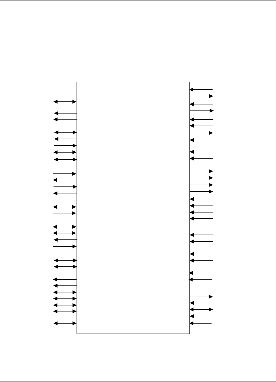
Signal Diagram
Copyright © 2015 Marvell CONFIDENTIAL Doc. No. MV-S109936-00 Rev. A
February 3, 2015, 1.00 Document Classification: Proprietary Page 41
1Package
1.1 Signal Diagram
Figure 2: Signal Diagram1234
1. Signals are muxed on dedicated pins. See Section 1.4, Pin Description, on page 46 for dedicated pin / muxed signal descriptions.
2. Some pins/signals are available on the 88-pin QFN only. See Section 1.4, Pin Description, on page 46.
3. RF_TR, USB OTG, XTAL_IN/OUT, and RESETn pins are dedicated. Others are muxed on GPIOs.
4. See Table 16, Power and Ground, on page 66 for power signals.
88MW300/302
GPIO Interface
GPIO_0 to GPIO_49
JTAG Interface
TDI
TCK
TDO
TMS
TRSTn
WLAN RF Interface
RF_TR
UART Interface
(UART0-UART2)
UARTx_TXD
UARTx_RXD
UARTx_CTSn
UARTx_RTSn
SSP Interface
(SSP0-SSP2)
SSPx_FRM
SSPx_CLK
SSPx_TXD
SSPx_RXD
GPTx_CHx GPT Interface
(GPT 0-GPT3,
Ch0-5 each)
GPT_CLKIN
Clock/Control
Interface WAKE_UP0
WAKE_UP1
XTAL32K_OUT
XTAL32K_IN
XTAL_OUT
XTAL_IN
RESETn
AUDIO_CLK
QSPI Interface
QSPI_CLK
QSPI_SSn
QSPI_D0
QSPI_D1
QSPI_D2
QSPI_D3
WLAN RF Front End
Interface
RF_CNTL0_N
RF_CNTL1_P
VOICE_N
VOICE_P
Voice
TS_INP
TS_INN
Temperature
Sensor Interface
DACB
DACA
DAC Interface
I2Cx_SDA I
2
C Interface
(I2C0-I2C1)
I2Cx_SCL
COMP_IN_P
COMP_IN_N
EXT_VREF
ADC/ACOMP Interface
(ADC0, Ch0-7)
ADC0_x / ACOMPx
ACOMP0_EDGE_PULS
E
ACOMP1_EDGE_PULS
E
ADC_DAC_TRIGGER0
ADC_DAC_TRIGGER1
ACOMP1_GPIO_OUT
ACOMP0_GPIO_OUT
LDO18
Comparator
Interface
USB OTG 2.0 Interface
USB_DP
USB_ID
USB_VBUS
USB_DM
USB_DRV_VBUS
xam1
uypvwincml8vcyp7azhga8189kcblgwl8g12a4v3hp-i72ogizr * Global Network Lighting &
Con
MARVELL CONFIDENTIAL, UNDER NDA# 12150208
m1u
ypvwincml8vcyp7azhga8189kcblgwl8g12a4v3hp-i72ogizr * Global Network Lighting & Con
trol In
MARVELL CONFIDENTIAL, UNDER NDA# 12150208
2fdrxam1uypvwincml8vcyp7azhga8189kcblgwl8g12a4v3hp-i72ogizr * Globa
l Net
88MW300/302
Datasheet
Doc. No. MV-S109936-00 Rev. A CONFIDENTIAL Copyright © 2015 Marvell
Page 42 Document Classification: Proprietary February 3, 2015, 1.00
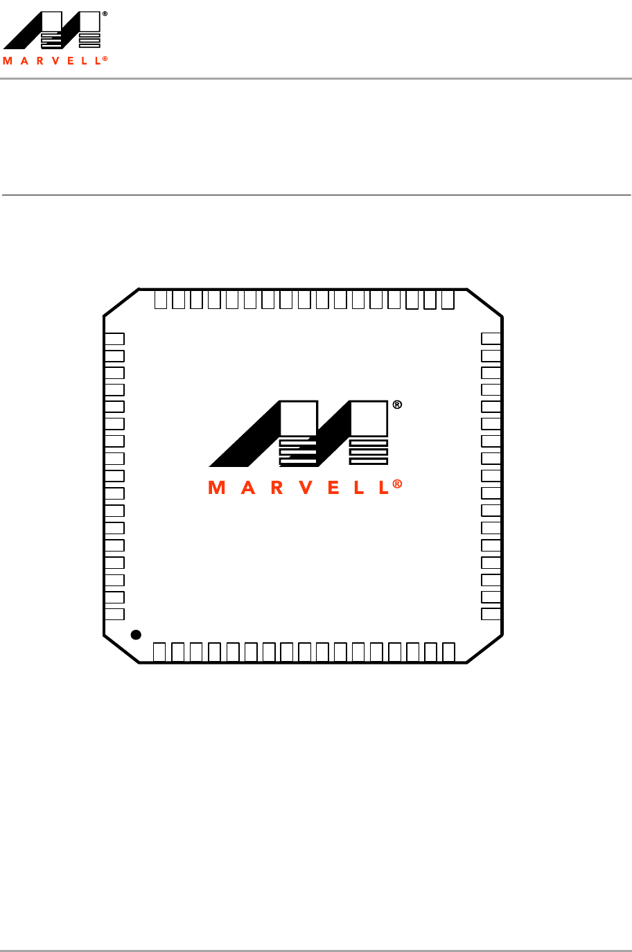
1.2 Pinout
1.2.1 Pinout—68-Pin QFN
Figure 3: Pinout—68-Pin QFN1
1. Connect pin 17 to ground.
68
67
66
65
64
63
62
61
60
59
58
57
56
55
54
53
52
88MW300
16
17
1
2
3
4
5
6
7
8
9
10
11
12
13
14
15
GPIO_27
GPIO_39
VDDIO_3
GPIO_40
GPIO_41
GPIO_46
GPIO_47
GPIO_48
GPIO_49
FLY18
VBAT_IN
FLY11
VBAT_IN
BUCK18_VX
LDO11_V18
LDO11_VOU
T
GPIO_16
VDDIO_1
VDD11
DNC
DNC
DNC
DNC
AVDD18
XTAL_OUT
XTAL_IN
AVDD18
AVDD18
AVDD18
18
19
20
21
22
23
24
25
26
27
28
29
30
31
32
33
34
GPIO_0
GPIO_1
GPIO_2
GPIO_3
V
DDIO_0
GPIO_4
GPIO_5
GPIO_6
GPIO_7
GPIO_8
GPIO_9
GPIO_10
AVDD18
AVDD18
AVDD33
RF_TR
NC
41
40
39
38
51
50
49
48
47
46
45
44
43
42
37
36
35
ISENSE
VDDIO_2
VDD11
VDDIO_AO
N
GPIO_26
GPIO_25
GPIO_24
GPIO_23
VTR_VDD3
3
GPIO_22
RES ETn
GPIO_33
GPIO_32
GPIO_31
GPIO_30
GPIO_29
GPIO_28
VDDIO_3
GPIO_42
GPIO_43
GPIO_44
GPIO_45
xam1
uypvwincml8vcyp7azhga8189kcblgwl8g12a4v3hp-i72ogizr * Global Network Lighting &
Con
MARVELL CONFIDENTIAL, UNDER NDA# 12150208
m1u
ypvwincml8vcyp7azhga8189kcblgwl8g12a4v3hp-i72ogizr * Global Network Lighting & Con
trol In
MARVELL CONFIDENTIAL, UNDER NDA# 12150208
2fdrxam1uypvwincml8vcyp7azhga8189kcblgwl8g12a4v3hp-i72ogizr * Globa
l Net
Package
Pinout
Copyright © 2015 Marvell CONFIDENTIAL Doc. No. MV-S109936-00 Rev. A
February 3, 2015, 1.00 Document Classification: Proprietary Page 43
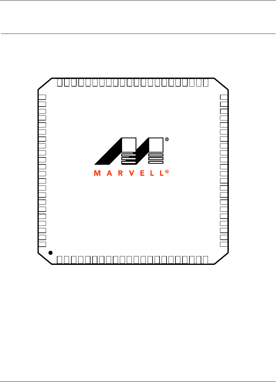
1.2.2 Pinout—88-Pin QFN
Figure 4: Pinout—88-Pin QFN1
1. Connect pin 22 to ground.
88
87
86
85
84
83
82
81
80
79
78
77
76
75
74
73
72
71
70
69
68
67
88MW302
51
50
49
48
66
65
64
63
62
61
60
59
58
57
56
55
54
53
52
47
46
45
23
24
25
26
27
28
29
30
31
32
33
34
35
36
37
38
39
40
41
42
43
44
16
17
18
19
1
2
3
4
5
6
7
8
9
10
11
12
13
14
15
20
21
22
GPIO_0
GPIO_1
GPIO_2
GPIO_3
V
DDIO_0
GPIO_4
GPIO_5
GPIO_6
GPIO_7
GPIO_8
GPIO_9
GPIO_10
GPIO_11
GPIO_12
GPIO_13
GPIO_14
GPIO_15
AVDD18
AVDD18
AVDD33
RF_TR
NC
USB_DM
USB_DP
USB_AVDD3
3
USB_ID
USB_VBUS
ISENSE
VDDIO_2
GPIO_33
GPIO_32
GPIO_31
GPIO_30
GPIO_29
GPIO_28
VDD11
VDDIO_AON
GPIO_26
GPIO_25
GPIO_24
GPIO_23
VTR_VDD33
GPIO_22
RESETn
VBAT_IN
BUCK18_VX
LDO11_V18
LDO11_VOU
T
GPIO_21
GPIO_20
GPIO_19
GPIO_18
GPIO_17
GPIO_16
VDDIO_1
VDD11
DNC
DNC
DNC
DNC
AVDD18
XTAL_OUT
XTAL_IN
AVDD18
AVDD18
AVDD18
GPIO_34
GPIO_35
GPIO_36
GPIO_37
GPIO_27
GPIO_38
GPIO_39
VDDIO_3
GPIO_40
GPIO_41
FLY18
VBAT_IN
FLY11
VDDIO_3
GPIO_46
GPIO_47
GPIO_48
GPIO_49
GPIO_42
GPIO_43
GPIO_44
GPIO_45
xam1
uypvwincml8vcyp7azhga8189kcblgwl8g12a4v3hp-i72ogiz
r * G
MARVELL CONFIDENTIAL, UNDER NDA
# 12
m1u
ypvwincml8vcyp7azhga8189kcblgwl8g12a4v3hp-i72ogizr * Global Network Lighting & Control Inc.
MARVELL CONFIDENTIAL, UNDER NDA# 12150208
MARVELL CONFIDENTIAL - UNAUTHORIZED DISTRIBUTION OR USE STR
ICTLY
88MW300/302
Datasheet
Doc. No. MV-S109936-00 Rev. A CONFIDENTIAL Copyright © 2015 Marvell
Page 44 Document Classification: Proprietary February 3, 2015, 1.00
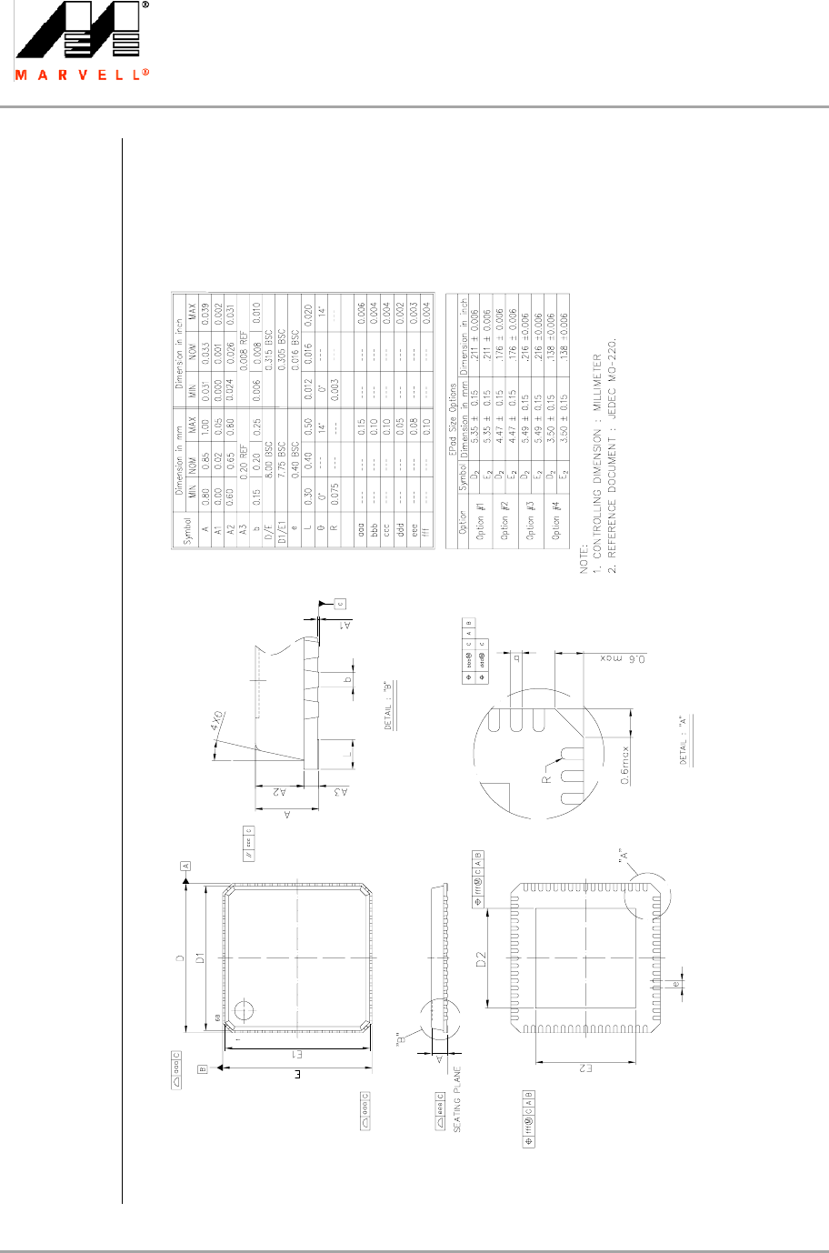
1.3 Mechanical Drawing
1.3.1 Mechanical Drawing—68-Pin QFN
Note: QFN package uses Epad size Option #3 only. See Section 22.4, Package Thermal Conditions, on page 315 for electrical
specifications. See Section 23.2, Package Marking, on page 336 for package marking.
Figure 5: Mechanical Drawing—68-Pin QFN
xam1
uypvwincml8vcyp7azhga8189kcblgwl8g12a4v3hp-i72ogiz
r * G
MARVELL CONFIDENTIAL, UNDER NDA
# 12
m1u
ypvwincml8vcyp7azhga8189kcblgwl8g12a4v3hp-i72ogizr * Global Network Lighting & Control Inc.
MARVELL CONFIDENTIAL, UNDER NDA# 12150208
MARVELL CONFIDENTIAL - UNAUTHORIZED DISTRIBUTION OR USE STR
ICTLY
Package
Mechanical Drawing
Copyright © 2015 Marvell CONFIDENTIAL Doc. No. MV-S109936-00 Rev. A
February 3, 2015, 1.00 Document Classification: Proprietary Page 45
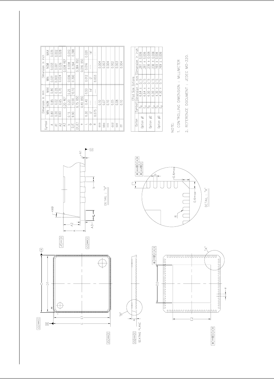
1.3.2 Mechanical Drawing—88-Pin QFN
Note: QFN package uses Epad size Option #3 only. See Section 22.4, Package Thermal Conditions, on page 315 for electrical
specifications. See Section 23.2, Package Marking, on page 336 for package marking.
Figure 6: Mechanical Drawing—88-Pin QFN
xam1
uypvwincml8vcyp7azhga8189kcblgwl8g12a4v3hp-i72ogizr * Global Network Lighting &
Con
MARVELL CONFIDENTIAL, UNDER NDA# 12150208
m1u
ypvwincml8vcyp7azhga8189kcblgwl8g12a4v3hp-i72ogizr * Global Network Lighting & Con
trol In
MARVELL CONFIDENTIAL, UNDER NDA# 12150208
2fdrxam1uypvwincml8vcyp7azhga8189kcblgwl8g12a4v3hp-i72ogizr * Globa
l Net
88MW300/302
Datasheet
Doc. No. MV-S109936-00 Rev. A CONFIDENTIAL Copyright © 2015 Marvell
Page 46 Document Classification: Proprietary February 3, 2015, 1.00
1.4 Pin Description
.
Table 2: Pin Types
Pin Type Description
I/O Digital input/output
I Digital input
O Digital output
A, I Analog input
A, O Analog output
NC No connect
DNC Do not connect
PWR Power
Ground Ground
Table 3: WLAN RF Interface
88-Pin 68-Pin Pin Name Type Supply Description
21 16 RF_TR A, I/O AVDD18 WLAN RF Interface (2.4 GHz Transmit/Receive)
Baseband input/output data
Table 4: WLAN RF Front End Interface
88-Pin 68-Pin Pin Name Type Supply Description
GPIO_44 RF_CNTL1_P A, O VDDIO_3 WLAN Radio Control 1
Power-down output high signal
GPIO_45 RF_CNTL0_N A, O VDDIO_3 WLAN Radio Control 0
Power-down output low signal

xam1
uypvwincml8vcyp7azhga8189kcblgwl8g12a4v3hp-i72ogizr * Global Network Lighting &
Con
MARVELL CONFIDENTIAL, UNDER NDA# 12150208
m1u
ypvwincml8vcyp7azhga8189kcblgwl8g12a4v3hp-i72ogizr * Global Network Lighting & Con
trol In
MARVELL CONFIDENTIAL, UNDER NDA# 12150208
2fdrxam1uypvwincml8vcyp7azhga8189kcblgwl8g12a4v3hp-i72ogizr * Globa
l Net
Package
Pin Description
Copyright © 2015 Marvell CONFIDENTIAL Doc. No. MV-S109936-00 Rev. A
February 3, 2015, 1.00 Document Classification: Proprietary Page 47
Table 5: USB 2.0 OTG Interface1
NOTE: Available on 88-pin package only (88MW302)
88-Pin 68-Pin Pin Name Type Supply Description
61 -- USB_VBUS A, I/O USB_AVDD33 USB VBUS Selection Input In Device Mode
Unused in host mode; I/O for OTG mode to
supply +5V@10mA during session
negotiation.
GPIO_27 -- USB_DRV_VBUS A, O VDDIO_3 Drive 5V on VBUS
0 = do not drive VBUS
1 = drive 5V on VBUS
The USB_DRV_VBUS port is connected to
the SoC pad to drive an external power
management chip to provide power for USB
VBUS.
62 -- USB_ID A, I USB_AVDD33 USB 2.0 OTG IDPIN
63 -- USB_AVDD33 A, I -- USB 3.3V Analog Power Supply
See Table 16, Power and Ground, on
page 66.
64 -- USB_DP A, I/O USB_AVDD33 USB 2.0 Bus Data+
65 -- USB_DM A, I/O USB_AVDD33 USB 2.0 Bus Data–
1. After POR, if USB is in host mode, USB_DPUSB_DM will be SE0. If USB is in device mode, USB_DP/USB_DM will be High-z.
Table 6: UART Interface1
88-Pin 68-Pin Signal Name Type Supply Description
GPIO_0 UART0_CTSn I VDDIO_0 UART 0 CTSn (active low)
GPIO_1 UART0_RTSn O VDDIO_0 UART 0 RTSn (active low)
GPIO_2 UART0_TXD O VDDIO_0 UART 0 TXD
GPIO_3 UART0_RXD I VDDIO_0 UART 0 RXD
GPIO_23 UART0_CTSn I VDDIO_AON UART 0 CTSn (active low)
GPIO_24 UART0_RXD I VDDIO_AON UART 0 RXD
GPIO_30 UART0_CTSn I VDDIO_2 UART 0 CTSn (active low)
GPIO_31 UART0_RTSn O VDDIO_2 UART 0 RTSn (active low)
GPIO_32 UART0_TXD O VDDIO_2 UART 0 TXD
GPIO_33 UART0_RXD I VDDIO_2 UART 0 RXD

xam1
uypvwincml8vcyp7azhga8189kcblgwl8g12a4v3hp-i72ogizr * Global Network Lighting &
Con
MARVELL CONFIDENTIAL, UNDER NDA# 12150208
m1u
ypvwincml8vcyp7azhga8189kcblgwl8g12a4v3hp-i72ogizr * Global Network Lighting & Con
trol In
MARVELL CONFIDENTIAL, UNDER NDA# 12150208
2fdrxam1uypvwincml8vcyp7azhga8189kcblgwl8g12a4v3hp-i72ogizr * Globa
l Net
88MW300/302
Datasheet
Doc. No. MV-S109936-00 Rev. A CONFIDENTIAL Copyright © 2015 Marvell
Page 48 Document Classification: Proprietary February 3, 2015, 1.00
GPIO_37 -- UART0_RTSn O VDDIO_3 UART 0 RTSn (active low)
GPIO_27 UART0_TXD O VDDIO_3 UART 0 TXD
GPIO_11 -- UART1_CTSn I VDDIO_0 UART 1 CTSn (active low)
GPIO_12 -- UART1_RTSn O VDDIO_0 UART 1 RTSn (active low)
GPIO_13 -- UART1_TXD O VDDIO_0 UART 1 TXD
GPIO_14 -- UART1_RXD I VDDIO_0 UART 1 RXD
GPIO_35 -- UART1_CTSn I VDDIO_3 UART 1 CTSn (active low)
GPIO_36 -- UART1_RTSn O VDDIO_3 UART 1 RTSn (active low)
GPIO_38 -- UART1_TXD O VDDIO_3 UART 1 TXD
GPIO_39 UART1_RXD I VDDIO_3 UART 1 RXD
GPIO_42 UART1_CTSn I VDDIO_3 UART 1 CTSn (active low)
GPIO_43 UART1_RTSn O VDDIO_3 UART 1 RTSn (active low)
GPIO_44 UART1_TXD O VDDIO_3 UART 1 TXD
GPIO_45 UART1_RXD I VDDIO_3 UART 1 RXD
GPIO_7 UART2_CTSn I VDDIO_0 UART 2 CTSn (active low)
GPIO_8 UART2_RTSn O VDDIO_0 UART 2 RTSn (active low)
GPIO_9 UART2_TXD O VDDIO_0 UART 2 TXD
GPIO_10 UART2_RXD I VDDIO_0 UART 2 RXD
GPIO_46 UART2_CTSn I VDDIO_3 UART 2 CTSn (active low)
GPIO_47 UART2_RTSn O VDDIO_3 UART 2 RTSn (active low)
GPIO_48 UART2_TXD O VDDIO_3 UART 2 TXD
GPIO_49 UART2_RXD I VDDIO_3 UART 2 RXD
1. All UART signals are muxed on GPIO pins. See Table 11, GPIO Interface, on page 53 for GPIO muxing.
Table 6: UART Interface1
88-Pin 68-Pin Signal Name Type Supply Description

xam1
uypvwincml8vcyp7azhga8189kcblgwl8g12a4v3hp-i72ogizr * Global Network Lighting &
Con
MARVELL CONFIDENTIAL, UNDER NDA# 12150208
m1u
ypvwincml8vcyp7azhga8189kcblgwl8g12a4v3hp-i72ogizr * Global Network Lighting & Con
trol In
MARVELL CONFIDENTIAL, UNDER NDA# 12150208
2fdrxam1uypvwincml8vcyp7azhga8189kcblgwl8g12a4v3hp-i72ogizr * Globa
l Net
Package
Pin Description
Copyright © 2015 Marvell CONFIDENTIAL Doc. No. MV-S109936-00 Rev. A
February 3, 2015, 1.00 Document Classification: Proprietary Page 49
Table 7: GPT Interface1
88-Pin 68-Pin Signal Name Type Supply Description
GPIO_0 GPT0_CH0 I/O VDDIO_0 General Purpose Timer 0, Channel 0
GPIO_1 GPT0_CH1 I/O VDDIO_0 General Purpose Timer 0, Channel 1
GPIO_2 GPT0_CH2 I/O VDDIO_0 General Purpose Timer 0, Channel 2
GPIO_3 GPT0_CH3 I/O VDDIO_0 General Purpose Timer 0, Channel 3
GPIO_4 GPT0_CH4 I/O VDDIO_0 General Purpose Timer 0, Channel 4
GPIO_5 GPT0_CH5 I/O VDDIO_0 General Purpose Timer 0, Channel 5
GPIO_35 -- GPT0_CLKIN I VDDIO_3 General Purpose Timer 0, Clock Input
GPIO_28 GPT1_CH0 I/O VDDIO_2 General Purpose Timer 1, Channel 0
GPIO_29 GPT1_CH1 I/O VDDIO_2 General Purpose Timer 1, Channel 1
GPIO_30 GPT1_CH2 I/O VDDIO_2 General Purpose Timer 1, Channel 2
GPIO_31 GPT1_CH3 I/O VDDIO_2 General Purpose Timer 1, Channel 3
GPIO_32 GPT1_CH4 I/O VDDIO_2 General Purpose Timer 1, Channel 4
GPIO_33 GPT1_CH5 I/O VDDIO_2 General Purpose Timer 1, Channel 5
GPIO_24 GPT1_CH5 I/O VDDIO_AON General Purpose Timer 1, Channel 5
GPIO_36 -- GPT1_CLKIN I VDDIO_3 General Purpose Timer 1, Clock Input
GPIO_11 -- GPT2_CH0 I/O VDDIO_0 General Purpose Timer 2, Channel 0
GPIO_12 -- GPT2_CH1 I/O VDDIO_0 General Purpose Timer 2, Channel 1
GPIO_13 -- GPT2_CH2 I/O VDDIO_0 General Purpose Timer 2, Channel 2
GPIO_14 -- GPT2_CH3 I/O VDDIO_0 General Purpose Timer 2, Channel 3
GPIO_15 -- GPT2_CH4 I/O VDDIO_0 General Purpose Timer 2, Channel 4
GPIO_37 -- GPT2_CH5 I/O VDDIO_3 General Purpose Timer 2, Channel 5
GPIO_38 -- GPT2_CLKIN I VDDIO_3 General Purpose Timer 2, Clock Input
GPIO_17 -- GPT3_CH0 I/O VDDIO_1 General Purpose Timer 3, Channel 0
GPIO_18 -- GPT3_CH1 I/O VDDIO_1 General Purpose Timer 3, Channel 1
GPIO_19 -- GPT3_CH2 I/O VDDIO_1 General Purpose Timer 3, Channel 2
GPIO_20 -- GPT3_CH3 I/O VDDIO_1 General Purpose Timer 3, Channel 3

xam1
uypvwincml8vcyp7azhga8189kcblgwl8g12a4v3hp-i72ogizr * Global Network Lighting &
Con
MARVELL CONFIDENTIAL, UNDER NDA# 12150208
m1u
ypvwincml8vcyp7azhga8189kcblgwl8g12a4v3hp-i72ogizr * Global Network Lighting & Con
trol In
MARVELL CONFIDENTIAL, UNDER NDA# 12150208
2fdrxam1uypvwincml8vcyp7azhga8189kcblgwl8g12a4v3hp-i72ogizr * Globa
l Net
88MW300/302
Datasheet
Doc. No. MV-S109936-00 Rev. A CONFIDENTIAL Copyright © 2015 Marvell
Page 50 Document Classification: Proprietary February 3, 2015, 1.00
GPIO_21 -- GPT3_CH4 I/O VDDIO_1 General Purpose Timer 3, Channel 4
GPIO_34 -- GPT3_CH5 I/O VDDIO_3 General Purpose Timer 3, Channel 5
GPIO_39 GPT3_CLKIN I VDDIO_3 General Purpose Timer 2, Clock Input
1. All GPT signals are muxed on GPIO pins. See Table 11, GPIO Interface, on page 53 for GPIO muxing.
Table 7: GPT Interface1
88-Pin 68-Pin Signal Name Type Supply Description
Table 8: SSP Interface1
88-Pin 68-Pin Pin Name Type Supply Description
GPIO_0 SSP0_CLK I/O VDDIO_0 SSP 0 Serial Clock
GPIO_1 SSP0_FRM I/O VDDIO_0 SSP 0 Frame Indicator
GPIO_2 SSP0_TXD O VDDIO_0 SSP 0 TXD
GPIO_3 SSP0_RXD I VDDIO_0 SSP 0 RXD
GPIO_30 SSP0_CLK I/O VDDIO_2 SSP 0 Serial Clock
GPIO_31 SSP0_FRM I/O VDDIO_2 SSP 0 Frame Indicator
GPIO_32 SSP0_TXD O VDDIO_2 SSP 0 TXD
GPIO_33 SSP0_RXD I VDDIO_2 SSP 0 RXD
GPIO_11 -- SSP1_CLK I/O VDDIO_0 SSP 1 Serial Clock
GPIO_12 -- SSP1_FRM I/O VDDIO_0 SSP 1 Frame Indicator
GPIO_13 -- SSP1_TXD O VDDIO_0 SSP 1 TXD
GPIO_14 -- SSP1_RXD I VDDIO_0 SSP 1 RXD
GPIO_18 -- SSP1_CLK I/O VDDIO_1 SSP 1 Serial Clock
GPIO_19 -- SSP1_FRM I/O VDDIO_1 SSP 1 Frame Indicator
GPIO_20 -- SSP1_TXD O VDDIO_1 SSP 1 TXD
GPIO_21 -- SSP1_RXD I VDDIO_1 SSP 1 RXD
GPIO_35 -- SSP1_CLK I/O VDDIO_3 SSP 1 Serial Clock
GPIO_36 -- SSP1_FRM I/O VDDIO_3 SSP 1 Frame Indicator

xam1
uypvwincml8vcyp7azhga8189kcblgwl8g12a4v3hp-i72ogizr * Global Network Lighting &
Con
MARVELL CONFIDENTIAL, UNDER NDA# 12150208
m1u
ypvwincml8vcyp7azhga8189kcblgwl8g12a4v3hp-i72ogizr * Global Network Lighting & Con
trol In
MARVELL CONFIDENTIAL, UNDER NDA# 12150208
2fdrxam1uypvwincml8vcyp7azhga8189kcblgwl8g12a4v3hp-i72ogizr * Globa
l Net
Package
Pin Description
Copyright © 2015 Marvell CONFIDENTIAL Doc. No. MV-S109936-00 Rev. A
February 3, 2015, 1.00 Document Classification: Proprietary Page 51
GPIO_38 -- SSP1_TXD O VDDIO_3 SSP 1 TXD
GPIO_39 SSP1_RXD I VDDIO_3 SSP 1 RXD
GPIO_42 SSP1_CLK I/O VDDIO_3 SSP 1 Serial Clock
GPIO_43 SSP1_FRM I/O VDDIO_3 SSP 1 Frame Indicator
GPIO_44 SSP1_TXD O VDDIO_3 SSP 1 TXD
GPIO_45 SSP1_RXD I VDDIO_3 SSP 1 RXD
GPIO_7 SSP2_CLK I/O VDDIO_0 SSP 2 Serial Clock
GPIO_8 SSP2_FRM I/O VDDIO_0 SSP 2 Frame Indicator
GPIO_9 SSP2_TXD O VDDIO_0 SSP 2 TXD
GPIO_10 SSP2_RXD I VDDIO_0 SSP 2 RXD
GPIO_46 SSP2_CLK I/O VDDIO_3 SSP 2 Serial Clock
GPIO_47 SSP2_FRM I/O VDDIO_3 SSP 2 Frame Indicator
GPIO_48 SSP2_TXD O VDDIO_3 SSP 2 TXD
GPIO_49 SSP2_RXD I VDDIO_3 SSP 2 RXD
1. All SSP signals are muxed on GPIO pins. See Table 11, GPIO Interface, on page 53 for GPIO muxing.
Table 8: SSP Interface1 (Continued)
88-Pin 68-Pin Pin Name Type Supply Description

xam1
uypvwincml8vcyp7azhga8189kcblgwl8g12a4v3hp-i72ogizr * Global Network Lighting &
Con
MARVELL CONFIDENTIAL, UNDER NDA# 12150208
m1u
ypvwincml8vcyp7azhga8189kcblgwl8g12a4v3hp-i72ogizr * Global Network Lighting & Con
trol In
MARVELL CONFIDENTIAL, UNDER NDA# 12150208
2fdrxam1uypvwincml8vcyp7azhga8189kcblgwl8g12a4v3hp-i72ogizr * Globa
l Net
88MW300/302
Datasheet
Doc. No. MV-S109936-00 Rev. A CONFIDENTIAL Copyright © 2015 Marvell
Page 52 Document Classification: Proprietary February 3, 2015, 1.00
Table 9: I2C Interface1
88-Pin 68-Pin Pin Name Type Supply Description
GPIO_4
GPIO_7
I2C0_SDA I/O VDDIO_0 I2C0 SDA
GPIO_5
GPIO_8
I2C0_SCL I/O VDDIO_0 I2C0 SCL
GPIO_6
GPIO_9
I2C1_SDA I/O VDDIO_0 I2C1 SDA
GPIO_10 I2C1_SCL I/O VDDIO_0 I2C1 SCL
GPIO_20 -- I2C0_SDA I/O VDDIO_1 I2C0 SDA
GPIO_21 -- I2C0_SCL I/O VDDIO_1 I2C0 SCL
GPIO_18 -- I2C1_SDA I/O VDDIO_1 I2C1 SDA
GPIO_17
GPIO_19
-- I2C1_SCL I/O VDDIO_1 I2C1 SCL
GPIO_25 I2C1_SDA I/O VDDIO_AON I2C1 SDA
GPIO_26 I2C1_SCL I/O VDDIO_AON I2C1 SCL
GPIO_28 I2C0_SDA I/O VDDIO_2 I2C1 SDA
GPIO_29 I2C0_SCL I/O VDDIO_2 I2C1 SCL
1. All I2C signals are muxed on GPIO pins. See Table 11, GPIO Interface, on page 53 for GPIO muxing.
Table 10: QSPI Interface1
88-Pin 68-Pin Pin Name Type Supply Description
GPIO_28 QSPI_SSn O VDDIO_2 QSPI Chip Select (active low)
GPIO_29 QSPI_CLK O VDDIO_2 QSPI Clock
GPIO_30 QSPI_D0 I/O VDDIO_2 QSPI Data 0
GPIO_31 QSPI_D1 I/O VDDIO_2 QSPI Data 1
GPIO_32 QSPI_D2 I/O VDDIO_2 QSPI Data 2
GPIO_33 QSPI_D3 I/O VDDIO_2 QSPI Data 3
1. QSPI signals are used for external Flash only. All QSPI signals are muxed on GPIO pins. See Table 11, GPIO Interface, on page 53 for
GPIO muxing.

xam1
uypvwincml8vcyp7azhga8189kcblgwl8g12a4v3hp-i72ogizr * Global Network Lighting &
Con
MARVELL CONFIDENTIAL, UNDER NDA# 12150208
m1u
ypvwincml8vcyp7azhga8189kcblgwl8g12a4v3hp-i72ogizr * Global Network Lighting & Con
trol In
MARVELL CONFIDENTIAL, UNDER NDA# 12150208
2fdrxam1uypvwincml8vcyp7azhga8189kcblgwl8g12a4v3hp-i72ogizr * Globa
l Net
Package
Pin Description
Copyright © 2015 Marvell CONFIDENTIAL Doc. No. MV-S109936-00 Rev. A
February 3, 2015, 1.00 Document Classification: Proprietary Page 53
Table 11: GPIO Interface 12
88-Pin 68-Pin Pin/Signal Name Type Supply Description
1 1 GPIO_0 I/O VDDIO_0 General Purpose I/O 0
GPT0_CH0 I/O General Purpose Timer 0, Channel 0
UART0_CTSn I UART 0 CTSn (active low)
SSP0_CLK I/O SSP 0 Serial Clock
2 2 GPIO_1 I/O VDDIO_0 General Purpose I/O 1
GPT0_CH1 I/O General Purpose Timer 0, Channel 1
UART0_RTSn O UART 0 RTSn (active low)
SSP0_FRM I/O SSP 0 Frame Indicator
3 3 GPIO_2 I/O VDDIO_0 General Purpose I/O 2
GPT0_CH2 I/O General Purpose Timer 0, Channel 2
UART0_TXD O UART 0 TXD
SSP0_TXD O SSP 0 TXD
4 4 GPIO_3 I/O VDDIO_0 General Purpose I/O 3
GPT0_CH3 I/O General Purpose Timer 0, Channel 3
UART0_RXD I UART 0 RXD
SSP0_RXD I SSP 0 RXD
6 6 GPIO_4 I/O VDDIO_0 General Purpose I/O 4
GPT0_CH4 I/O General Purpose Timer 0, Channel 4
I2C0_SDA I/O I2C0 SDA
AUDIO_CLK O Audio Clock
AUPLL Audio clock output provided by Audio
PLL for external codec.
7 7 GPIO_5 I/O VDDIO_0 General Purpose I/O 5
GPT0_CH5 I/O General Purpose Timer 0, Channel 5
I2C0_SCL I/O I2C0 SCL

xam1
uypvwincml8vcyp7azhga8189kcblgwl8g12a4v3hp-i72ogizr * Global Network Lighting &
Con
MARVELL CONFIDENTIAL, UNDER NDA# 12150208
m1u
ypvwincml8vcyp7azhga8189kcblgwl8g12a4v3hp-i72ogizr * Global Network Lighting & Con
trol In
MARVELL CONFIDENTIAL, UNDER NDA# 12150208
2fdrxam1uypvwincml8vcyp7azhga8189kcblgwl8g12a4v3hp-i72ogizr * Globa
l Net
88MW300/302
Datasheet
Doc. No. MV-S109936-00 Rev. A CONFIDENTIAL Copyright © 2015 Marvell
Page 54 Document Classification: Proprietary February 3, 2015, 1.00
8 8 GPIO_6 I/O VDDIO_0 General Purpose I/O 6
TDO O JTAG Test Data
I2C1_SDA I/O I2C1 SDA
9 9 GPIO_7 I/O VDDIO_0 General Purpose I/O 7
TCK I JTAG Test Clock
UART2_CTSn I UART 2 CTSn (active low)
SSP2_CLK I/O SSP 2 Serial Clock
I2C0_SDA I/O I2C0 SDA
10 10 GPIO_8 I/O VDDIO_0 General Purpose I/O 8
TMS I/O JTAG Controller Select
UART2_RTSn O UART 2 RTSn (active low)
SSP2_FRM I/O SSP_2 Frame Indicator
I2C0_SCL I/O I2C0 SCL
11 11 GPIO_9 I/O VDDIO_0 General Purpose I/O 9
TDI I JTAG Test Data
UART2_TXD O UART 2 TXD
SSP2_TXD O SSP 2 TXD
I2C1_SDA I/O I2C1 SDA
12 12 GPIO_10 I/O VDDIO_0 General Purpose I/O 10
TRSTn I JTAG Test Reset (active low)
UART2_RXD I UART 2 RXD
SSP2_TXD O SSP 2 RXD
I2C1_SCL I/O I2C1 SCL
Table 11: GPIO Interface 1 (Continued)2
88-Pin 68-Pin Pin/Signal Name Type Supply Description

xam1
uypvwincml8vcyp7azhga8189kcblgwl8g12a4v3hp-i72ogizr * Global Network Lighting &
Con
MARVELL CONFIDENTIAL, UNDER NDA# 12150208
m1u
ypvwincml8vcyp7azhga8189kcblgwl8g12a4v3hp-i72ogizr * Global Network Lighting & Con
trol In
MARVELL CONFIDENTIAL, UNDER NDA# 12150208
2fdrxam1uypvwincml8vcyp7azhga8189kcblgwl8g12a4v3hp-i72ogizr * Globa
l Net
Package
Pin Description
Copyright © 2015 Marvell CONFIDENTIAL Doc. No. MV-S109936-00 Rev. A
February 3, 2015, 1.00 Document Classification: Proprietary Page 55
13 -- GPIO_11 I/O VDDIO_0 General Purpose I/O 11
GPT2_CH0 I/O General Purpose Timer 2, Channel 0
UART1_CTSn I UART 1 CTSn (active low)
SSP1_CLK I/O SSP 1 Serial Clock
14 -- GPIO_12 I/O VDDIO_0 General Purpose I/O 12
GPT2_CH1 I/O General Purpose Timer 2, Channel 1
UART1_RTSn O UART 1 RTSn (active low)
SSP1_FRM I/O SSP 1 Frame Indicator
15 -- GPIO_13 I/O VDDIO_0 General Purpose I/O 13
GPT2_CH2 I/O General Purpose Timer 2, Channel 2
UART1_TXD O UART 1 TXD
SSP1_TXD O SSP 1 TXD
16 -- GPIO_14 I/O VDDIO_0 General Purpose I/O 14
GPT2_CH3 I/O General Purpose Timer 2, Channel 3
UART1_RXD I UART 1 RXD
SSP1_RXD I SSP 1 RXD
17 -- GPIO_15 I/O VDDIO_0 General Purpose I/O 15
GPT2_CH4 I/O General Purpose Timer 2, Channel 4
35 30 GPIO_16 I/O VDDIO_1 General Purpose I/O 16
CON[5] I/O Configuration Bit
See Table 17, Configuration Pins, on
page 67.
AUDIO_CLK O Audio Clock
AUPLL Audio clock output provided by Audio
PLL for external codec.
Table 11: GPIO Interface 1 (Continued)2
88-Pin 68-Pin Pin/Signal Name Type Supply Description
xam1
uypvwincml8vcyp7azhga8189kcblgwl8g12a4v3hp-i72ogizr * Global Network Lighting &
Con
MARVELL CONFIDENTIAL, UNDER NDA# 12150208
m1u
ypvwincml8vcyp7azhga8189kcblgwl8g12a4v3hp-i72ogizr * Global Network Lighting & Con
trol In
MARVELL CONFIDENTIAL, UNDER NDA# 12150208
2fdrxam1uypvwincml8vcyp7azhga8189kcblgwl8g12a4v3hp-i72ogizr * Globa
l Net
88MW300/302
Datasheet
Doc. No. MV-S109936-00 Rev. A CONFIDENTIAL Copyright © 2015 Marvell
Page 56 Document Classification: Proprietary February 3, 2015, 1.00
36 -- GPIO_17 I/O VDDIO_1 General Purpose I/O 17
GPT3_CH0 I/O General Purpose Timer 3, Channel 0
I2C1_SCL I/O I2C1 SCL
37 -- GPIO_18 I/O VDDIO_1 General Purpose I/O 18
GPT3_CH1 I/O General Purpose Timer 3, Channel 1
I2C1_SDA I/O I2C1 SDA
SSP1_CLK I/O SSP 1 Serial Clock
38 -- GPIO_19 I/O VDDIO_1 General Purpose I/O 19
GPT3_CH2 I/O General Purpose Timer 3, Channel 2
I2C1_SCL I/O I2C1 SDA
SSP1_FRM I/O SSP 1 Frame Indicator
39 -- GPIO_20 I/O VDDIO_1 General Purpose I/O 20
GPT3_CH3 I/O General Purpose Timer 3, Channel 3
I2C0_SDA I/O I2C0 SDA
SSP1_TXD O SSP 1 TXD
40 -- GPIO_21 I/O VDDIO_1 General Purpose I/O 21
GPT3_CH4 I/O General Purpose Timer 3, Channel 4
I2C0_SCL I/O I2C0 SCL
SSP1_RXD I SSP 1 RXD
46 36 GPIO_22 I/O VDDIO_
AON
General Purpose I/O 22
WAKE_UP0 I Wake-Up 0
Table 11: GPIO Interface 1 (Continued)2
88-Pin 68-Pin Pin/Signal Name Type Supply Description

xam1
uypvwincml8vcyp7azhga8189kcblgwl8g12a4v3hp-i72ogizr * Global Network Lighting &
Con
MARVELL CONFIDENTIAL, UNDER NDA# 12150208
m1u
ypvwincml8vcyp7azhga8189kcblgwl8g12a4v3hp-i72ogizr * Global Network Lighting & Con
trol In
MARVELL CONFIDENTIAL, UNDER NDA# 12150208
2fdrxam1uypvwincml8vcyp7azhga8189kcblgwl8g12a4v3hp-i72ogizr * Globa
l Net
Package
Pin Description
Copyright © 2015 Marvell CONFIDENTIAL Doc. No. MV-S109936-00 Rev. A
February 3, 2015, 1.00 Document Classification: Proprietary Page 57
47 37 GPIO_23 I/O VDDIO_
AON
General Purpose I/O 23
UART0_CTSn I UART 0 CTSn (active low)
WAKE_UP1 I Wake-Up 1
COMP_IN_P I LDO18 Comparator Input, Positive
Positive input to LDO18 comparator.
48 38 GPIO_24 I/O VDDIO_
AON
General Purpose I/O 24
UART0_RXD I UART 0 RXD
GPT1_CH5 I/O General Purpose Timer 1, Channel 5
COMP_IN_N I LDO18 Comparator Input, Negative
Negative input to LDO18 comparator.
49 39 GPIO_25 I/O VDDIO_
AON
General Purpose I/O 25
XTAL32K_IN I 32.768 kHz Crystal Input
I2C1_SDA I/O I2C1 SDA
50 40 GPIO_26 I/O VDDIO_
AON
General Purpose I/O 26
XTAL32K_OUT O 32.768 kHz Crystal Output
I2C1_SCL I/O I2C1 SCL
66 51 GPIO_27 I/O VDDIO_3 General Purpose I/O 27
-- USB_DRV_VBUS O Drive 5V on VBUS
51 UART0_TXD O UART 0 TXD
51 CON[4] I/O Configuration Bit
See Table 17, Configuration Pins, on
page 67.
52 42 GPIO_28 I/O VDDIO_2 General Purpose I/O 28
QSPI_SSn O QSPI Chip Select (active low)
I2C0_SDA I/O I2C0 SDA
GPT1_CH0 I/O General Purpose Timer 1, Channel 0
Table 11: GPIO Interface 1 (Continued)2
88-Pin 68-Pin Pin/Signal Name Type Supply Description

xam1
uypvwincml8vcyp7azhga8189kcblgwl8g12a4v3hp-i72ogizr * Global Network Lighting &
Con
MARVELL CONFIDENTIAL, UNDER NDA# 12150208
m1u
ypvwincml8vcyp7azhga8189kcblgwl8g12a4v3hp-i72ogizr * Global Network Lighting & Con
trol In
MARVELL CONFIDENTIAL, UNDER NDA# 12150208
2fdrxam1uypvwincml8vcyp7azhga8189kcblgwl8g12a4v3hp-i72ogizr * Globa
l Net
88MW300/302
Datasheet
Doc. No. MV-S109936-00 Rev. A CONFIDENTIAL Copyright © 2015 Marvell
Page 58 Document Classification: Proprietary February 3, 2015, 1.00
53 43 GPIO_29 I/O VDDIO_2 General Purpose I/O 29
QSPI_CLK O QSPI Clock
I2C0_SCL I/O I2C0 SCL
GPT1_CH1 I/O General Purpose Timer 1, Channel 1
54 44 GPIO_30 I/O VDDIO_2 General Purpose I/O 30
QSPI_D0 I/O QSPI Data 0
UART0_CTSn I UART 0 CTSn (active low)
SSP0_CLK I/O SSP 0 Serial Clock
GPT1_CH2 I/O General Purpose Timer 1, Channel 2
55 45 GPIO_31 I/O VDDIO_2 General Purpose I/O 31
QSPI_D1 I/O QSPI Data 1
UART0_RTSn O UART 0 RTSn (active low)
SSP0_FRM I/O SSP 0 Frame Indicator
GPT1_CH3 I/O General Purpose Timer 1, Channel 3
56 46 GPIO_32 I/O VDDIO_2 General Purpose I/O 32
QSPI_D2 I/O QSPI Data 2
UART0_TXD O UART 0 TXD
SSP0_TXD O SSP 0 TXD
GPT1_CH4 I/O General Purpose Timer 1, Channel 4
57 47 GPIO_33 I/O VDDIO_2 General Purpose I/O 33
QSPI_D3 I/O QSPI Data 3
UART0_RXD I UART 0 RXD
SSP0_RXD I SSP 0 RXD
GPT1_CH5 I/O General Purpose Timer 1, Channel 5
Table 11: GPIO Interface 1 (Continued)2
88-Pin 68-Pin Pin/Signal Name Type Supply Description

xam1
uypvwincml8vcyp7azhga8189kcblgwl8g12a4v3hp-i72ogizr * Global Network Lighting &
Con
MARVELL CONFIDENTIAL, UNDER NDA# 12150208
m1u
ypvwincml8vcyp7azhga8189kcblgwl8g12a4v3hp-i72ogizr * Global Network Lighting & Con
trol In
MARVELL CONFIDENTIAL, UNDER NDA# 12150208
2fdrxam1uypvwincml8vcyp7azhga8189kcblgwl8g12a4v3hp-i72ogizr * Globa
l Net
Package
Pin Description
Copyright © 2015 Marvell CONFIDENTIAL Doc. No. MV-S109936-00 Rev. A
February 3, 2015, 1.00 Document Classification: Proprietary Page 59
67 -- GPIO_34 I/O VDDIO_3 General Purpose I/O 34
GPT3_CH5 I/O General Purpose Timer 3, Channel 5
68 -- GPIO_35 I/O VDDIO_3 General Purpose I/O 35
GPT0_CLKIN I General Purpose Timer 0, Clock Input
UART1_CTSn I UART 1 CTSn (active low)
SSP1_CLK I/O SSP 1 Serial Clock
69 -- GPIO_36 I/O VDDIO_3 General Purpose I/O 36
GPT1_CLKIN I General Purpose Timer 1, Clock Input
UART1_RTSn O UART 1 RTSn (active low)
SSP1_FRM I/O SSP 1 Frame Indicator
70 -- GPIO_37 I/O VDDIO_3 General Purpose I/O 37
GPT2_CH5 I/O General Purpose Timer 2, Channel 5
UART0_RTSn O UART 0 RTSn (active low)
71 -- GPIO_38 I/O VDDIO_3 General Purpose I/O 38
GPT2_CLKIN I General Purpose Timer 2, Clock Input
UART1_TXD O UART 1 TXD
SSP1_TXD O SSP 1 TXD
72 52 GPIO_39 I/O VDDIO_3 General Purpose I/O 39
GPT3_CLKIN I General Purpose Timer 2, Clock Input
UART1_RXD I UART 1 RXD
SSP1_RXD I SSP 1 RXD
Table 11: GPIO Interface 1 (Continued)2
88-Pin 68-Pin Pin/Signal Name Type Supply Description

xam1
uypvwincml8vcyp7azhga8189kcblgwl8g12a4v3hp-i72ogizr * Global Network Lighting &
Con
MARVELL CONFIDENTIAL, UNDER NDA# 12150208
m1u
ypvwincml8vcyp7azhga8189kcblgwl8g12a4v3hp-i72ogizr * Global Network Lighting & Con
trol In
MARVELL CONFIDENTIAL, UNDER NDA# 12150208
2fdrxam1uypvwincml8vcyp7azhga8189kcblgwl8g12a4v3hp-i72ogizr * Globa
l Net
88MW300/302
Datasheet
Doc. No. MV-S109936-00 Rev. A CONFIDENTIAL Copyright © 2015 Marvell
Page 60 Document Classification: Proprietary February 3, 2015, 1.00
75 55 GPIO_40 I/O VDDIO_3 General Purpose I/O 40
ADC_DAC_TRIGGER0 I ADC/DAC External Trigger 0
ACOMP0_GPIO_OUT O ACOMP0 GPIO Output
ACOMP0 output synchronous or
asynchronous level signals.
ACOMP1_GPIO_OUT O ACOMP1 GPIO Output
ACOMP1 output synchronous or
asynchronous level signals.
76 56 GPIO_41 I/O VDDIO_3 General Purpose I/O 41
ADC_DAC_TRIGGER1 I ADC/DAC External Trigger 1
ACOMP0_EDGE_
PULSE
O ACOMP Edge Pulse 0
Output pulse aligned with synchronized
comparison result.
ACOMP1_EDGE_
PULSE
O ACOMP Edge Pulse 1
Output pulse aligned with synchronized
comparison result.
78 58 GPIO_42 I/O VDDIO_3 General Purpose I/O 42
ADC0_0 / ACOMP0 /
TS_INP / VOICE_P
A, I ADC0 Channel 0
ACOMP0 Channel 0
ACOMP1 Channel 0
Temperature sensor remote sensing positive
input
Voice sensing positive input
UART1_CTSn I UART 1 CTSn (active low)
SSP1_CLK I/O SSP 1 Serial Clock
Table 11: GPIO Interface 1 (Continued)2
88-Pin 68-Pin Pin/Signal Name Type Supply Description

xam1
uypvwincml8vcyp7azhga8189kcblgwl8g12a4v3hp-i72ogizr * Global Network Lighting &
Con
MARVELL CONFIDENTIAL, UNDER NDA# 12150208
m1u
ypvwincml8vcyp7azhga8189kcblgwl8g12a4v3hp-i72ogizr * Global Network Lighting & Con
trol In
MARVELL CONFIDENTIAL, UNDER NDA# 12150208
2fdrxam1uypvwincml8vcyp7azhga8189kcblgwl8g12a4v3hp-i72ogizr * Globa
l Net
Package
Pin Description
Copyright © 2015 Marvell CONFIDENTIAL Doc. No. MV-S109936-00 Rev. A
February 3, 2015, 1.00 Document Classification: Proprietary Page 61
79 59 GPIO_43 I/O VDDIO_3 General Purpose I/O 43
ADC0_1 / ACOMP1 /
TS_INN / DACB /
VOICE_N
A, I ADC0 Channel 1
ACOMP0 Channel 1
ACOMP1 Channel 1
Temperature sensor remote sensing
negative input
Voice sensing negative input
UART1_RTSn O UART 1 RTSn (active low)
SSP1_FRM I/O SSP 1 Frame Indicator
80 60 GPIO_44 I/O VDDIO_3 General Purpose I/O 44
ADC0_2 / ACOMP2 /
DACA
A, I ADC0 Channel 2
ACOMP0 Channel 2
ACOMP1 Channel 2
DAC Channel A output
UART1_TXD O UART 1 TXD
SSP1_TXD O SSP 1 TXD
RF_CNTL1_P O WLAN Radio Control 1
81 61 GPIO_45 I/O VDDIO_3 General Purpose I/O 45
ADC0_3 / ACOMP3 /
EXT_VREF
A, I ADC0 Channel 3
ACOMP0 Channel 3
ACOMP1 Channel 3
ADC or DAC external voltage reference input
UART1_RXD I UART 1 RXD
SSP1_RXD I SSP 1 RXD
RF_CNTL0_N O WLAN Radio Control 0
82 62 GPIO_46 I/O VDDIO_3 General Purpose I/O 46
ADC0_4 / ACOMP4 A, I ADC0 Channel 4
ACOMP0 Channel 4
ACOMP1 Channel 4
UART2_CTSn I UART 2 CTSn (active low)
SSP2_CLK I/O SSP 2 Serial Clock
Table 11: GPIO Interface 1 (Continued)2
88-Pin 68-Pin Pin/Signal Name Type Supply Description

xam1
uypvwincml8vcyp7azhga8189kcblgwl8g12a4v3hp-i72ogizr * Global Network Lighting &
Con
MARVELL CONFIDENTIAL, UNDER NDA# 12150208
m1u
ypvwincml8vcyp7azhga8189kcblgwl8g12a4v3hp-i72ogizr * Global Network Lighting & Con
trol In
MARVELL CONFIDENTIAL, UNDER NDA# 12150208
2fdrxam1uypvwincml8vcyp7azhga8189kcblgwl8g12a4v3hp-i72ogizr * Globa
l Net
88MW300/302
Datasheet
Doc. No. MV-S109936-00 Rev. A CONFIDENTIAL Copyright © 2015 Marvell
Page 62 Document Classification: Proprietary February 3, 2015, 1.00
83 63 GPIO_47 I/O VDDIO_3 General Purpose I/O 47
ADC0_5 / ACOMP5 A, I ADC0 Channel 5
ACOMP0 Channel 5
ACOMP1 Channel 5
UART2_RTSn O UART 2 RTSn (active low)
SSP2_FRM I/O SSP 2 Frame Indicator
84 64 GPIO_48 I/O VDDIO_3 General Purpose I/O 48
ADC0_6 / ACOMP6 A, I ADC0 Channel 6
ACOMP0 Channel 6
ACOMP1 Channel 6
UART2_TXD O UART 2 TXD
SSP2_TXD O SSP 2 TXD
85 65 GPIO_49 I/O VDDIO_3 General Purpose I/O 49
ADC0_7 / ACOMP7 A, I ADC0 Channel 7
ACOMP0 Channel 7
ACOMP1 Channel 7
UART2_RXD I UART 2 RXD
SSP2_RXD I SSP 2 RXD
1. GPIO_11 to GPIO_15, GPIO_17 to GPIO_21, GPIO_34 to GPIO_38 I/O and associated muxing available on 88-pin QFN only.
2. All GPIO pins are pull-up high after POR.
Table 11: GPIO Interface 1 (Continued)2
88-Pin 68-Pin Pin/Signal Name Type Supply Description

xam1
uypvwincml8vcyp7azhga8189kcblgwl8g12a4v3hp-i72ogizr * Global Network Lighting &
Con
MARVELL CONFIDENTIAL, UNDER NDA# 12150208
m1u
ypvwincml8vcyp7azhga8189kcblgwl8g12a4v3hp-i72ogizr * Global Network Lighting & Con
trol In
MARVELL CONFIDENTIAL, UNDER NDA# 12150208
2fdrxam1uypvwincml8vcyp7azhga8189kcblgwl8g12a4v3hp-i72ogizr * Globa
l Net
Package
Pin Description
Copyright © 2015 Marvell CONFIDENTIAL Doc. No. MV-S109936-00 Rev. A
February 3, 2015, 1.00 Document Classification: Proprietary Page 63
Table 12: Clock/Control Interface1
88-Pin 68-Pin Pin/Signal
Name Type Supply Description
26 21 XTAL_IN A, I AVDD18 Crystal Oscillator Input
27 22 XTAL_OUT A, O AVDD18 Crystal Oscillator Output
Connect to ground when an external oscillator used.
GPIO_25 XTAL32K_IN A, I VDDIO_AON 32.768 kHz Crystal Input
GPIO_26 XTAL32K_OUT A, O VDDIO_AON 32.768 kHz Crystal Output
GPIO_22 WAKE_UP0 I VDDIO_AON Wake-Up 0
GPIO_23 WAKE_UP1 I VDDIO_AON Wake-Up 1
GPIO_4
GPIO_16
AUDIO_CLK VDDIO_0 Audio Clock
AUPLL audio clock output provided by audio PLL for
external codec.
45 35 RESETn I VDDIO_AON Chip Reset (active low)
1. The XTAL32K_IN/OUT and WAKE_UP0/1 signals are muxed on GPIO pins. See Table 11, GPIO Interface, on page 53 for GPIO muxing.

xam1
uypvwincml8vcyp7azhga8189kcblgwl8g12a4v3hp-i72ogizr * Global Network Lighting &
Con
MARVELL CONFIDENTIAL, UNDER NDA# 12150208
m1u
ypvwincml8vcyp7azhga8189kcblgwl8g12a4v3hp-i72ogizr * Global Network Lighting & Con
trol In
MARVELL CONFIDENTIAL, UNDER NDA# 12150208
2fdrxam1uypvwincml8vcyp7azhga8189kcblgwl8g12a4v3hp-i72ogizr * Globa
l Net
88MW300/302
Datasheet
Doc. No. MV-S109936-00 Rev. A CONFIDENTIAL Copyright © 2015 Marvell
Page 64 Document Classification: Proprietary February 3, 2015, 1.00
Table 13: ADC/DAC/ACOMP Interface1
88-Pin 68-Pin Pin Name Type Supply Description
GPIO_40 ACOMP0_GPIO_OUT O VDDIO_3 ACOMP0 GPIO Output
ACOMP0 output synchronous or
asynchronous level signals
ACOMP1_GPIO_OUT O VDDIO_3 ACOMP1 GPIO Output
ACOMP1 output synchronous or
asynchronous level signals
ADC_DAC_TRIGGER0 I VDDIO_3 ADC/DAC External Trigger 0
GPIO_41 ACOMP0_EDGE_PULSE O VDDIO_3 ACOMP Edge Pulse 0
Output pulse aligned with synchronized
comparison result.
ACOMP1_EDGE_PULSE O VDDIO_3 ACOMP Edge Pulse 1
Output pulse aligned with synchronized
comparison result.
ADC_DAC_TRIGGER1 I VDDIO_3 ADC/DAC External Trigger 1
GPIO_49 ADC0_7 / ACOMP7 A, I VDDIO_3 ADC0 Channel 7
ACOMP0 Channel 7
ACOMP1 Channel 7
GPIO_48 ADC0_6 / ACOMP6 A, I VDDIO_3 ADC0 Channel 6
ACOMP0 Channel 6
ACOMP1 Channel 6
GPIO_47 ADC0_5 / ACOMP5 A, I VDDIO_3 ADC0 Channel 5
ACOMP0 Channel 5
ACOMP1 Channel 5
GPIO_46 ADC0_4 / ACOMP4 A, I VDDIO_3 ADC0 Channel 4
ACOMP0 Channel 4
ACOMP1 Channel 4
GPIO_45 ADC0_3 / ACOMP3 /
EXT_VREF
A, I VDDIO_3 ADC0 Channel 3
ACOMP0 Channel 3
ACOMP1 Channel 3
ADC or DAC external voltage reference
input
GPIO_44 ADC0_2 / ACOMP2 /
DACA
A, I VDDIO_3 ADC0 Channel 2
ACOMP0 Channel 2
ACOMP1 Channel 2
DAC Channel A output

xam1
uypvwincml8vcyp7azhga8189kcblgwl8g12a4v3hp-i72ogizr * Global Network Lighting &
Con
MARVELL CONFIDENTIAL, UNDER NDA# 12150208
m1u
ypvwincml8vcyp7azhga8189kcblgwl8g12a4v3hp-i72ogizr * Global Network Lighting & Con
trol In
MARVELL CONFIDENTIAL, UNDER NDA# 12150208
2fdrxam1uypvwincml8vcyp7azhga8189kcblgwl8g12a4v3hp-i72ogizr * Globa
l Net
Package
Pin Description
Copyright © 2015 Marvell CONFIDENTIAL Doc. No. MV-S109936-00 Rev. A
February 3, 2015, 1.00 Document Classification: Proprietary Page 65
GPIO_43 ADC0_1 / ACOMP1 /
TS_INN / DACB /
VOICE_N
A, I VDDIO_3 ADC0 Channel 1
ACOMP0 Channel 1
ACOMP1 Channel 1
Temperature sensor remote sensing
negative input
Voice sensing negative input
GPIO_42 ADC0_0 / ACOMP0 /
TS_INP / VOICE_P
A, I VDDIO_3 ADC0 Channel 0
ACOMP0 Channel 0
ACOMP1 Channel 0
Temperature sensor remote sensing
positive input
Voice sensing positive input
1. All ADC/DAC/ACOMP signals are muxed on GPIO pins. See Table 11, GPIO Interface, on page 53 for GPIO muxing.
Table 13: ADC/DAC/ACOMP Interface1 (Continued)
88-Pin 68-Pin Pin Name Type Supply Description
Table 14: LDO18 Comparator Interface1
88-Pin 68-Pin Pin Name Type Supply Description
GPIO_23 COMP_IN_P A, I VDDIO_AON LDO18 Comparator Input, Positive
Positive input to LDO18 comparator.
GPIO_24 COMP_IN_N A, I VDDIO_AON LDO18 Comparator Input, Negative
Positive input to LDO18 comparator.
1. All COMP signals are muxed on GPIO pins. See Table 11, GPIO Interface, on page 53 for GPIO muxing.
Table 15: JTAG Interface1
88-Pin 68-Pin Signal Name Type Supply Description
GPIO_6 TDO O VDDIO_0 JTAG Test Data
GPIO_7 TCK I VDDIO_0 JTAG Test Clock
GPIO_8 TMS I/O VDDIO_0 JTAG Controller Select
GPIO_9 TDI I VDDIO_0 JTAG Test Data
GPIO_10 TRSTn I VDDIO_0 JTAG Test Reset I/O (active low)
1. All JTAG signals are muxed on GPIO pins. See Table 11, GPIO Interface, on page 53 for GPIO muxing.

xam1
uypvwincml8vcyp7azhga8189kcblgwl8g12a4v3hp-i72ogizr * Global Network Lighting &
Con
MARVELL CONFIDENTIAL, UNDER NDA# 12150208
m1u
ypvwincml8vcyp7azhga8189kcblgwl8g12a4v3hp-i72ogizr * Global Network Lighting & Con
trol In
MARVELL CONFIDENTIAL, UNDER NDA# 12150208
2fdrxam1uypvwincml8vcyp7azhga8189kcblgwl8g12a4v3hp-i72ogizr * Globa
l Net
88MW300/302
Datasheet
Doc. No. MV-S109936-00 Rev. A CONFIDENTIAL Copyright © 2015 Marvell
Page 66 Document Classification: Proprietary February 3, 2015, 1.00
Table 16: Power and Ground
NOTE: See Section 22.2, Recommended Operating Conditions, on page 314 for ratings.
88-Pin 68-Pin Pin Name Type Description
33
59
28
49
VDD11 PWR 1.1V Core Power Supply Input
5 5 VDDIO_0 PWR I/O Digital Power Supply
34 29 VDDIO_1
58 48 VDDIO_2
77 57 VDDIO_3
73 53
51 41 VDDIO_AON
60 50 VTR_VDD33 PWR 3.3V OTP Analog Power Supply
63 -- USB_AVDD33 PWR 3.3V USB Analog Power Supply
74 54 ISENSE -- USB Current Source
Connect pin to ground with resistance.
20 15 AVDD33 PWR 3.3V Analog Power Supply
18
19
23
24
25
28
13
14
18
19
20
23
AVDD18 PWR 1.8V Analog Power Supply
41 31 LDO11_VOUT PWR 1.1V LV LDO Voltage Output
42 32 LDO11_V18 -- BUCK18 Inductor Connection
43 33 BUCK18_VX -- BUCK18 Inductor Connection
44
87
34
67
VBAT_IN PWR LDO VBAT Input
This pin must be connected to VBAT/V33 input even if
BUCK18 is not used.
86 66 FLY18 -- 1.8V LDO Fly Capacitor to Ground Connection
88 68 FLY11 -- 1.1V LDO Fly Capacitor to Ground Connection
22 17 NC NC No Connect
NOTE: CONNECT THESE PINS to GROUND.
29
30
31
32
24
25
26
27
DNC DNC Do Not Connect
Do not connect these pins. Leave these pins floating.

xam1
uypvwincml8vcyp7azhga8189kcblgwl8g12a4v3hp-i72ogizr * Global Network Lighting &
Con
MARVELL CONFIDENTIAL, UNDER NDA# 12150208
m1u
ypvwincml8vcyp7azhga8189kcblgwl8g12a4v3hp-i72ogizr * Global Network Lighting & Con
trol In
MARVELL CONFIDENTIAL, UNDER NDA# 12150208
2fdrxam1uypvwincml8vcyp7azhga8189kcblgwl8g12a4v3hp-i72ogizr * Globa
l Net
Package
Configuration Pins
Copyright © 2015 Marvell CONFIDENTIAL Doc. No. MV-S109936-00 Rev. A
February 3, 2015, 1.00 Document Classification: Proprietary Page 67
1.5 Configuration Pins
Table 17 shows the pins used as configuration inputs to set parameters following a reset. The
definition of these pins changes immediately after reset to their usual function. To set a configuration
bit to 0, attach a 100 kΩ resistor from the pin to ground. No external circuitry is required to set a
configuration bit to 1.
Table 17: Configuration Pins
Configuration
Bits Pin Name Configuration Function
CON[5] GPIO_16 Boot Options
00 = boot from UART
01 = reserved
10 = boot from USB
11 = boot from Flash (default)
CON[4] GPIO_27
This device complies with part 15 of the FCC Rules. Operation is subject to the following two conditions: (1) This
device may not cause harmful interference, and (2) this device must accept any interference received, including
interference that may cause undesired operation.
Changes or modifications not expressly approved by the party responsible for compliance could void the user's
authority to operate the equipment.
NOTE: This equipment has been tested and found to comply with the limits for a Class B digital device, pursuant
to Part 15 of the FCC Rules. These limits are designed to provide reasonable protection against harmful
interference in a residential installation. This equipment generates, uses and can radiate radio frequency energy and,
if not installed and used in accordance with the instructions, may cause harmful interference to radio
communications. However, there is no guarantee that interference will not occur in a particular installation. If this
equipment does cause harmful interference to radio or television reception, which can be determined by turning the
equipment off and on, the user is encouraged to try to correct the interference by one or more of the following
measures:
-- Reorient or relocate the receiving antenna.
-- Increase the separation between the equipment and receiver.
-- Connect the equipment into an outlet on a circuit different from that to which the receiver is connected.
-- Consult the dealer or an experienced radio/TV technician for help.
FCC Radiation Exposure Statement
The modular can be installed or integrated in mobile or fix devices only. This modular cannot be installed in any
portable device, for example, USB dongle like transmitters is forbidden.
This modular complies with FCC RF radiation exposure limits set forth for an uncontrolled environment. This
transmitter must not be co-located or operating in conjunction with any other antenna or transmitter. This modular
must be installed and operated with a minimum distance of 20 cm between the radiator and user body.
If the FCC identification number is not visible when the module is installed inside another device, then the outside
of the device into which the module is installed must also display a label referring to the enclosed module. This
exterior label can use wording such as the following: “Contains Transmitter Module FCC ID: YCJGTIMW302"
or "Contains FCC ID: YCJGTIMW302”
when the module is installed inside another device, the user manual of this device must contain below warning
statements;
1. This device complies with Part 15 of the FCC Rules. Operation is subject to the following two conditions:
(1) This device may not cause harmful interference.
(2) This device must accept any interference received, including interference that may cause undesired operation.
2. Changes or modifications not expressly approved by the party responsible for compliance could void the user's
authority to operate the equipment.
This device must be installed and operated with a minimum distance of 20 cm between the radiator and user body.