Guangzhou Shirui Electronics RK3399 Android Module User Manual AP6255 datasheet V1 1 04262015
Guangzhou Shirui Electronics Co., Ltd Android Module AP6255 datasheet V1 1 04262015
Users Manual
AMPAK Technology Inc. www.ampak.com.tw Proprietary & Confidential Information
Doc. NO:
正基
正基正基
正基科技股份有限公司
科技股份有限公司科技股份有限公司
科技股份有限公司
SPECIFICATION
SPEC. NO.:
::
: REV: 1.1
DATE:
::
: 04. 26. 2015
PRODUCT NAME:
::
: AP6255
APPROVED CHECKED PREPARED DCC ISSUE
NAME

AMPAK Technology Inc. www.ampak.com.tw Proprietary & Confidential Information
Doc. NO:
1
AMPAK
AP6255
WiFi 11ac + Bluetooth 4.1
Module Spec Sheet
AP6255 Datasheet
AMPAK Technology Inc. www.ampak.com.tw Proprietary & Confidential Information
Doc. NO:
2
Revision History
Date Revision Content Revised By
Version
2015/04/09 - Preliminary Gary 1.0
2015/04/26 - Add GPIO pin definiion Gary 1.1

AP6255 Datasheet
AMPAK Technology Inc. www.ampak.com.tw Proprietary & Confidential Information
Doc. NO:
3
Contents
Contents ................................................................................................................... 3
1. Introduction ......................................................................................................... 4
2. Features............................................................................................................... 5
3. Deliverables ........................................................................................................ 6
3.1 Deliverables .................................................................................................... 6
3.2 Regulatory certifications ................................................................................. 6
4. General Specification ......................................................................................... 7
4.1 General Specification ...................................................................................... 7
4.2 Voltages .......................................................................................................... 7
4.2.1 Absolute Maximum Ratings .................................................................... 7
4.2.2 Recommended Operating Rating ........................................................... 7
The module requires two power supplies: VBAT and VDDIO. ......................... 7
5. Wi-Fi RF Specification ........................................................................................ 8
5.1 2.4GHz RF Specification................................................................................. 8
5.1 5GHz RF Specification.................................................................................. 10
6. Bluetooth Specification .................................................................................... 13
6.1 Bluetooth Specification ................................................................................. 13
7. Pin Assignments ............................................................................................... 14
7.1 Pin Outline .................................................................................................... 14
7.2 Pin Definition ................................................................................................ 14
8. Dimensions ....................................................................................................... 16
8.1 Physical Dimensions .................................................................................... 16
8.2 Layout Recommendation .............................................................................. 17
9. External clock reference .................................................................................. 18
10.1 SDIO Pin Description .................................................................................. 19
10. Host Interface Timing Diagram ........................................................................ 20
10.1 Power-up Sequence Timing Diagram ......................................................... 20
10.2 SDIO Default Mode Timing Diagram........................................................... 22
10.3 SDIO High Speed Mode Timing Diagram ................................................... 23
10.4 SDIO Bus Timing Specifications in SDR Modes ......................................... 24
10.5 SDIO Bus Timing Specifications in DDR50 Mode ....................................... 26
11. Recommended Reflow Profile ......................................................................... 28
Solder Paste definition .......................................................................................... 29
12. Package Information ........................................................................................ 30
12.1 Label ........................................................................................................... 30
Label C
Inner box label . .................................................................................... 30
Label D
Carton box label . ................................................................................. 30

AP6255 Datasheet
AMPAK Technology Inc. www.ampak.com.tw Proprietary & Confidential Information
Doc. NO:
4
12.2 Dimension ................................................................................................... 31
12.3 MSL Level / Storage Condition ................................................................... 33
1. Introduction
AMPAK Technology would like to announce a low-cost and low-power consumption module
which has all of the Wi-Fi, Bluetooth functionalities. The highly integrated module makes the
possibilities of web browsing, VoIP, Bluetooth headsets applications. With seamless roaming
capabilities and advanced security, also could interact with different vendors’
802.11a/b/g/n/ac Access Points in the wireless LAN.
The wireless module complies with IEEE 802.11 a/b/g/n/ac standard and it can achieve up
to a speed of 433.3Mbps with single stream in 802.11ac draft to connect to the wireless LAN.
The integrated module provides SDIO interface for Wi-Fi, UART / PCM interface for
Bluetooth.
This compact module is a total solution for a combination of Wi-Fi + BT technologies. The
module is specifically developed for Smart phones and Portable devices.
AP6255 Datasheet
AMPAK Technology Inc. www.ampak.com.tw Proprietary & Confidential Information
Doc. NO:
5
2. Features
IEEE 802.11a/b/g/n/ac dual-band radio with virtual-simultaneous dual-band operation
Single-stream spatial multiplexing up to 433.3 Mbps data rate.
Supports 20, 40, 80 MHz channels with optional SGI(256 QAM modulation)
Bluetooth V4.0+EDR with integrated Class 1 PA and Low Energy (BLE) support
Concurrent Bluetooth, and WLAN operation
Simultaneous BT/WLAN receive with single antenna
Supports standard SDIO v3.0 and backward compatible with SDIO v2.0 host interfaces.
- SDIO v3.0(4-bit) — up to 208 MHz clock rate in SDR104 mode
BT host digital interface:
- UART (up to 4 Mbps)
IEEE Co-existence technologies are integrated die solution
ECI — enhanced coexistence support, ability to coordinate BT SCO transmissions
around WLAN receives
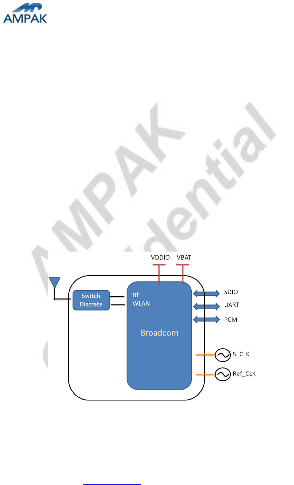
A simplified block diagram of the module is depicted in the figure below.

AP6255 Datasheet
AMPAK Technology Inc. www.ampak.com.tw Proprietary & Confidential Information
Doc. NO:
6
3. Deliverables
3.1 Deliverables
The following products and software will be part of the product.
Module with packaging
Evaluation Kits
Software utility for integration, performance test.
Product Datasheet.
Agency certified pre-tested report with the adapter board.
3.2 Regulatory certifications
The product delivery is a pre-tested module, without the module level certification. For
module approval, the platform’s antennas are required for the certification.
AP6255 Datasheet
AMPAK Technology Inc. www.ampak.com.tw Proprietary & Confidential Information
Doc. NO:
7
4. General Specification
4.1 General Specification
4.2 Voltages
4.2.1 Absolute Maximum Ratings
Symbol Description Min.
Max.
Unit
VBAT Input supply Voltage -0.5
6 V
VDDIO Digital/Bluetooth/SDIO/ I/O Voltage -0.5
3.9 V
4.2.2 Recommended Operating Rating
The module requires two power supplies: VBAT and VDDIO.
Min. Typ. Max. Unit
Operating Temperature -30 25 85 deg.C
VBAT 3.13 3.6 4.8 V
VDDIO 1.71 1.8 3.63 V
Model Name AP6255
Product Description Support Wi-Fi/Bluetooth functionalities
Dimension L x W x H: 12 x 12 x 1.5 (typical) mm
WiFi Interface SDIO v2.0/v3.0
BT Interface UART / PCM
Operating temperature
-30°C to 85°C
Storage temperature -40°C to 85°C
Humidity Operating Humidity 10% to 95% Non-Condensing
Storage Humidity 5% to 95% Non
-
Condensing
AP6255 Datasheet
AMPAK Technology Inc. www.ampak.com.tw Proprietary & Confidential Information
Doc. NO:
8
5. Wi-Fi RF Specification
5.1 2.4GHz RF Specification
Conditions : VBAT=3.6V ; VDDIO=3.3V ; Temp:25°C
Feature Description
WLAN Standard IEEE 802.11b/g/n/ac, WiFi compliant
Frequency Range 2.400 GHz ~ 2.497 GHz (2.4 GHz ISM Band)
Number of Channels
2.4GHz:Ch1 ~ Ch14
Modulation
802.11b : DQPSK, DBPSK, CCK
802.11g/n : 64-QAM,16-QAM, QPSK, BPSK
802.11ac : 256-QAM, 64-QAM,16-QAM, QPSK, BPSK
Output Power
802.11b /CCK : 16 dBm ± 1.5 dB @ EVM ≤ -9dB
802.11g /64-QAM(R=3/4) : 15 dBm ± 1.5 dB @ EVM ≤ -25dB
802.11n /64-QAM(R=5/6) : 14 dBm ± 1.5 dB @ EVM ≤ -28dB
Receive Sensitivity
(11b) @8% PER
- 1Mbps PER @ -96 dBm, typical
- 2Mbps PER @ -90 dBm, typical
- 5.5Mbps PER @ -88 dBm, typical
- 11Mbps PER @ -87 dBm, typical
Receive Sensitivity
(11g) @10% PER
- 6Mbps PER @ -90 dBm, typical
- 9Mbps PER @ -88 dBm, typical
- 12Mbps PER @ -87 dBm, typical
- 18Mbps PER @ -85 dBm, typical
- 24Mbps PER @ -83 dBm, typical
- 36Mbps PER @ -80 dBm, typical
- 48Mbps PER @ -76 dBm, typical
- 54Mbps PER @ -74 dBm, typical
Receive Sensitivity
(11n,20MHz)
@10% PER
- MCS=0 PER @ -89 dBm, typical
- MCS=1 PER @ -85 dBm, typical
- MCS=2 PER @ -84 dBm, typical
- MCS=3 PER @ -80 dBm, typical
- MCS=4 PER @ -77 dBm, typical
- MCS=5 PER @ -75 dBm, typical
- MCS=6 PER @ -72 dBm, typical
- MCS=7 PER @ -71 dBm, typical
Receive Sensitivity
(11n,40MHz)
- MCS=0 PER @ -89 dBm, typical
- MCS=1 PER @ -85 dBm, typical
AP6255 Datasheet
AMPAK Technology Inc. www.ampak.com.tw Proprietary & Confidential Information
Doc. NO:
9
@10% PER - MCS=2 PER @ -84 dBm, typical
- MCS=3 PER @ -80 dBm, typical
- MCS=4 PER @ -76 dBm, typical
- MCS=5 PER @ -72 dBm, typical
- MCS=6 PER @ -70 dBm, typical
- MCS=7 PER @ -69 dBm, typical
Receive Sensitivity
(11ac,20MHz)
@10% PER
- MCS=0 PER @ -90 dBm, typical
- MCS=1 PER @ -87 dBm, typical
- MCS=2 PER @ -86 dBm, typical
- MCS=3 PER @ -82 dBm, typical
- MCS=4 PER @ -79 dBm, typical
- MCS=5 PER @ -75 dBm, typical
- MCS=6 PER @ -73 dBm, typical
- MCS=7 PER @ -72 dBm, typical
- MCS=8 PER @ -67 dBm, typical
Receive Sensitivity
(11ac,40MHz)
@10% PER
- MCS=0 PER @ -88 dBm, typical
- MCS=1 PER @ -85 dBm, typical
- MCS=2 PER @ -83 dBm, typical
- MCS=3 PER @ -80 dBm, typical
- MCS=4 PER @ -77 dBm, typical
- MCS=5 PER @ -72 dBm, typical
- MCS=6 PER @ -71 dBm, typical
- MCS=7 PER @ -69 dBm, typical
- MCS=8 PER @ -65 dBm, typical
- MCS=9 PER @ -64 dBm, typical
Maximum Input Level
802.11b : -10dBm
802.11g/n : -20dBm
802.11ac : -30dBm
Antenna Reference Small antennas with 0~2 dBi peak gain
AP6255 Datasheet
AMPAK Technology Inc. www.ampak.com.tw Proprietary & Confidential Information
Doc. NO:
10
5.1 5GHz RF Specification
Conditions : VBAT=3.6V ; VDDIO=3.3V ; Temp:25°C
Feature Description
WLAN Standard IEEE 802.11a/b/g/n/ac, Wi-Fi compliant
Frequency Range 4.900 GHz ~ 5.845 GHz (5.0 GHz ISM Band)
Number of Channels
5.0GHz:Please see the table
1
Modulation 802.11a/n : 64-QAM,16-QAM, QPSK, BPSK
802.11ac : 256-QAM, 64-QAM,16-QAM, QPSK, BPSK
Output Power
802.11a /64-QAM(R=3/4) : 14 dBm ± 1.5 dB @ EVM ≤ -25dB
802.11n /64-QAM(R=5/6) : 13 dBm ± 1.5 dB @ EVM ≤ -28dB
802.11ac/256-QAM(R=3/4) : 12 dBm ± 1.5 dB @ EVM ≤ -30dB
802.11ac/256-QAM(R=5/6) : 10 dBm ± 1.5 dB @ EVM ≤ -32dB
Receive Sensitivity
(11a, 20MHz) @10%
PER
- 6Mbps PER @ -91 dBm, typical
- 9Mbps PER @ -89 dBm, typical
- 12Mbps PER @ -88 dBm, typical
- 18Mbps PER @ -86 dBm, typical
- 24Mbps PER @ -82 dBm, typical
- 36Mbps PER @ -79 dBm, typical
- 48Mbps PER @ -74 dBm, typical
- 54Mbps PER @ -73 dBm, typical
Receive Sensitivity
(11n,20MHz)
@10% PER
- MCS=0 PER @ -90 dBm, typical
- MCS=1 PER @ -88 dBm, typical
- MCS=2 PER @ -85 dBm, typical
- MCS=3 PER @ -82 dBm, typical
- MCS=4 PER @ -78 dBm, typical
- MCS=5 PER @ -74 dBm, typical
- MCS=6 PER @ -72 dBm, typical
- MCS=7 PER @ -71 dBm, typical
Receive Sensitivity
(11n,40MHz)
@10% PER
- MCS=0 PER @ -88 dBm, typical
- MCS=1 PER @ -85 dBm, typical
- MCS=2 PER @ -83 dBm, typical
- MCS=3 PER @ -79 dBm, typical
- MCS=4 PER @ -76 dBm, typical
- MCS=5 PER @ -71 dBm, typical
- MCS=6 PER @ -70 dBm, typical
- MCS=7 PER @ -68 dBm, typical
AP6255 Datasheet
AMPAK Technology Inc. www.ampak.com.tw Proprietary & Confidential Information
Doc. NO:
11
Receive Sensitivity
(11ac,20MHz)
@10% PER
- MCS=0 PER @ -89 dBm, typical
- MCS=1 PER @ -87 dBm, typical
- MCS=2 PER @ -84 dBm, typical
- MCS=3 PER @ -81 dBm, typical
- MCS=4 PER @ -77 dBm, typical
- MCS=5 PER @ -73 dBm, typical
- MCS=6 PER @ -71 dBm, typical
- MCS=7 PER @ -70 dBm, typical
- MCS=8 PER @ -66 dBm, typical
Receive Sensitivity
(11ac,40MHz)
@10% PER
- MCS=0 PER @ -87 dBm, typical
- MCS=1 PER @ -83 dBm, typical
- MCS=2 PER @ -81 dBm, typical
- MCS=3 PER @ -78 dBm, typical
- MCS=4 PER @ -75 dBm, typical
- MCS=5 PER @ -70 dBm, typical
- MCS=6 PER @ -68 dBm, typical
- MCS=7 PER @ -66 dBm, typical
- MCS=8 PER @ -64 dBm, typical
- MCS=9 PER @ -63 dBm, typical
Receive Sensitivity
(11ac,80MHz)
@10% PER
- MCS=0 PER @ -83 dBm, typical
- MCS=1 PER @ -80 dBm, typical
- MCS=2 PER @ -78 dBm, typical
- MCS=3 PER @ -74 dBm, typical
- MCS=4 PER @ -71 dBm, typical
- MCS=5 PER @ -69 dBm, typical
- MCS=6 PER @ -65 dBm, typical
- MCS=7 PER @ -63 dBm, typical
- MCS=8 PER @ -60 dBm, typical
- MCS=9 PER @ -59 dBm, typical
Maximum Input Level
802.11a/n : -20dBm
802.11ac : -30dBm
Antenna Reference Small antennas with 0~2 dBi peak gain
AP6255 Datasheet
AMPAK Technology Inc. www.ampak.com.tw Proprietary & Confidential Information
Doc. NO:
12
15GHz Channel table
Band (GHz) Operating Channel
Numbers
Channel center
frequencies(MHz)
5.15GHz~5.25GHz
36 5180
40 5200
44 5220
48 5240
5.25GHz~5.35GHz
52 5260
56 5280
60 5300
64 5320
5.5GHz~5.7GHz
100 5500
104 5520
108 5540
112 5560
116 5580
120 5600
124 5620
128 5640
132 5660
136 5680
140 5700
5.725GHz~5.825GHz
149 5745
153 5765
157 5785
161 5805
165 5825
AP6255 Datasheet
AMPAK Technology Inc. www.ampak.com.tw Proprietary & Confidential Information
Doc. NO:
13
6. Bluetooth Specification
6.1 Bluetooth Specification
Conditions : VBAT=3.6V ; VDDIO=3.3V ; Temp:25°C
Feature Description
General Specification
Bluetooth Standard Bluetooth V4.0 of 1, 2 and 3 Mbps.
Host Interface UART
Antenna Reference Small antennas with 0~2 dBi peak gain
Frequency Band 2402 MHz ~ 2480 MHz
Number of Channels 79 channels
Modulation FHSS, GFSK, DPSK, DQPSK
RF Specification
Min. Typical. Max.
Output Power (Class 1.5) 9 dBm
Output Power (Class 2) 2 dBm
Sensitivity @ BER=0.1%
for GFSK (1Mbps) -86 dBm
Sensitivity @ BER=0.01%
for π/4-DQPSK (2Mbps) -86 dBm
Sensitivity @ BER=0.01%
for 8DPSK (3Mbps) -80 dBm
Maximum Input Level
GFSK (1Mbps) :-20dBm
π/4-DQPSK (2Mbps) :-20dBm
8DPSK (3Mbps) :-20dBm
AP6255 Datasheet
AMPAK Technology Inc. www.ampak.com.tw Proprietary & Confidential Information
Doc. NO:
14
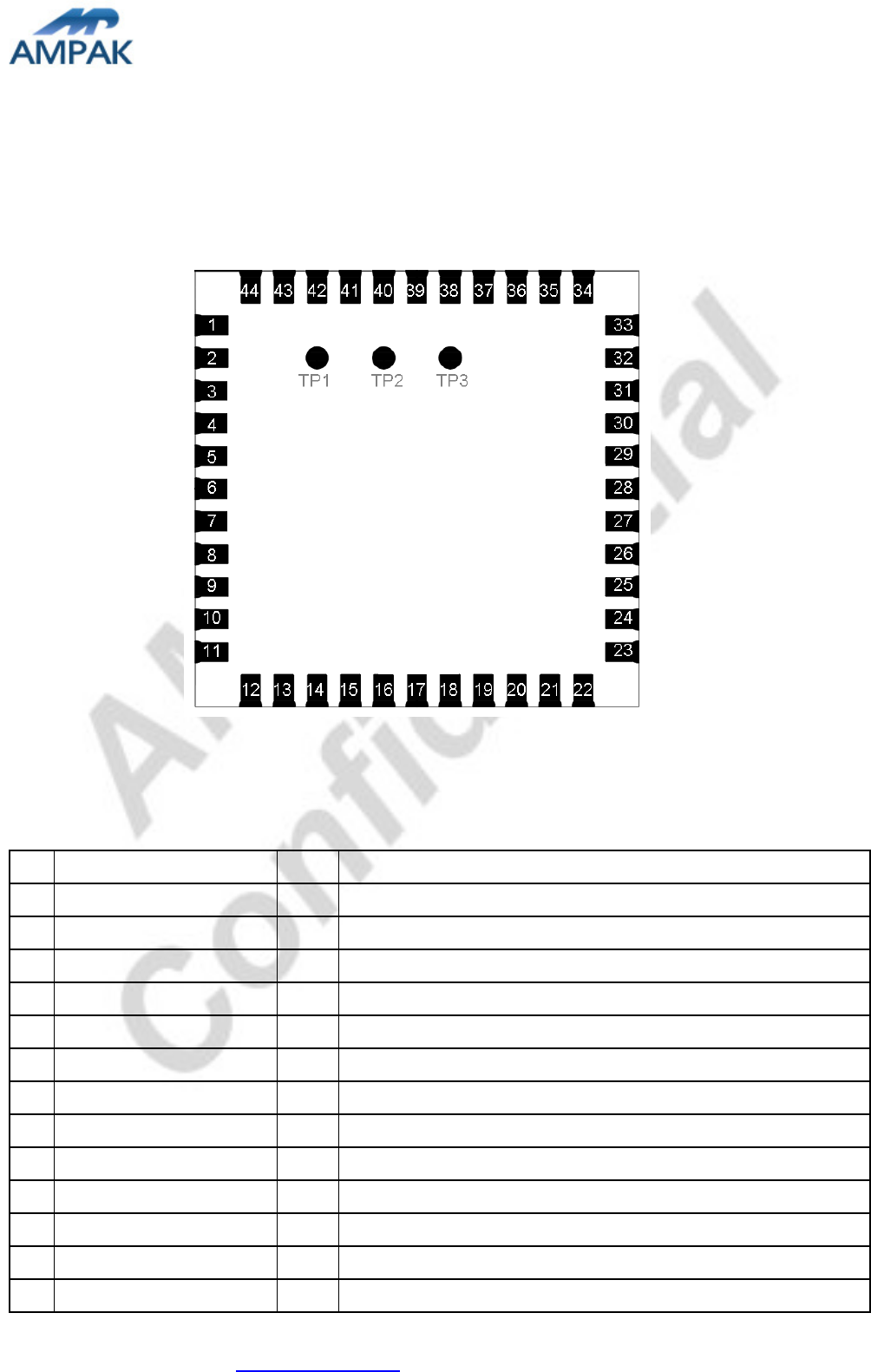
7. Pin Assignments
7.1 Pin Outline
< TOP VIEW >
7.2 Pin Definition
NO
Name Type
Description
1 GND - Ground connections
2 WL_BT_ANT I/O RF I/O port
3 GND - Ground connections
4 NC - Floating (Don’t connected to ground)
5 NC - Floating (Don’t connected to ground)
6 BT_WAKE I HOST wake-up Bluetooth device
7 BT_HOST_WAKE O Bluetooth device to wake-up HOST
8 NC - Floating (Don’t connected to ground)
9 VBAT P Main power voltage source input
10
XTAL_IN I Crystal input
11
XTAL_OUT O Crystal output
12
WL_REG_ON I Power up/down internal regulators used by WiFi section
13
WL_HOST_WAKE O WLAN to wake-up HOST
AP6255 Datasheet
AMPAK Technology Inc. www.ampak.com.tw Proprietary & Confidential Information
Doc. NO:
15
14
SDIO_DATA_2 I/O SDIO data line 2
15
SDIO_DATA_3 I/O SDIO data line 3
16
SDIO_DATA_CMD I/O SDIO command line
17
SDIO_DATA_CLK I/O SDIO clock line
18
SDIO_DATA_0 I/O SDIO data line 0
19
SDIO_DATA_1 I/O SDIO data line 1
20
GND - Ground connections
21
VIN_LDO_OUT P Internal Buck voltage generation pin
22
VDDIO P I/O Voltage supply input
23
VIN_LDO P Internal Buck voltage generation pin
24
LPO I External Low Power Clock input (32.768KHz)
25
PCM_OUT O PCM Data output
26
PCM_CLK I/O PCM clock
27
PCM_IN I PCM data input
28
PCM_SYNC I/O PCM sync signal
29
SDIO_VSEL I/O SDIO mode selection pin
30
NC - Floating (Don’t connected to ground)
31
GND - Ground connections
32
NC - Floating (Don’t connected to ground)
33
GND - Ground connections
34
BT_REG_ON I Power up/down internal regulators used by BT section
35
NC - Floating (Don’t connected to ground)
36
GND - Ground connections
37
GPIO_6 I/O GPIO configuration pin
38
GPIO_3 I/O GPIO configuration pin
39
GPIO_5 I/O GPIO configuration pin
40
GPIO_2 I/O GPIO configuration pin
41
UART_RTS_N O Bluetooth UART interface
42
UART_TXD O Bluetooth UART interface
43
UART_RXD I Bluetooth UART interface
44
UART_CTS_N I Bluetooth UART interface
45
TP1(NC) - Floating (Don’t connected to ground)
46
TP2(NC) - Floating (Don’t connected to ground)
47
TP3(NC) - Floating (Don’t connected to ground)
AP6255 Datasheet
AMPAK Technology Inc. www.ampak.com.tw Proprietary & Confidential Information
Doc. NO:
16
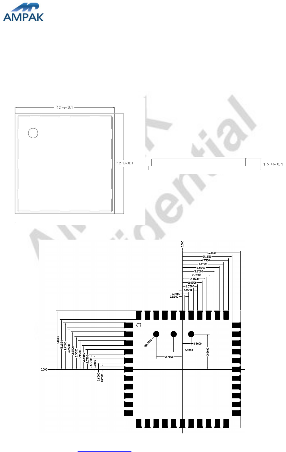
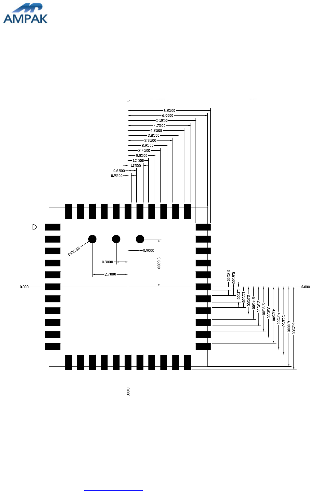
8. Dimensions
8.1 Physical Dimensions
(Unit: mm)
< TOP VIEW > < Side View >
< TOP VIEW >
AP6255 Datasheet
AMPAK Technology Inc. www.ampak.com.tw Proprietary & Confidential Information
Doc. NO:
17
8.2 Layout Recommendation
(Unit: mm)
< TOP VIEW >
AP6255 Datasheet
AMPAK Technology Inc. www.ampak.com.tw Proprietary & Confidential Information
Doc. NO:
18
9. External clock reference
External LPO signal characteristics
Parameter Specification Units
Nominal input frequency 32.768 kHz
Frequency accuracy 30
±
ppm
Duty cycle 30 - 70 %
Input signal amplitude 400 to 1800 mV, p-p
Signal type Square-wave -
Input impedance >100k
<5
Ω
pF
Clock jitter (integrated over 300Hz – 15KHz) <1 Hz
Output high voltage 0.7Vio - Vio V
AP6255 Datasheet
AMPAK Technology Inc. www.ampak.com.tw Proprietary & Confidential Information
Doc. NO:
19
10.1 SDIO Pin Description
All three package options of the WLAN section provide support for SDIO version 3.0
including the new UHS-I modes:
DS: Default speed up to 25MHz (3.3V signaling).
HS: High speed up to 50MH (3.3V signaling).
SDR12: SDR up to 25MHz (1.8V signaling).
SDR25: SDR up to 50MHz (1.8V signaling).
SDR50: SDR up to 100MHz (1.8V signaling).
SDR104: SDR up to 208MHz (1.8V signaling).
DDR50: DDR up to 50MHz (1.8V signaling).
The SDIO interface also has the ability to map the interrupt signal on to a GPIO pin for
applications requiring an interrupt different from the one provided by SDIO interface. The
ability to force control of gated clocks from within the device is also provided.
The following three functions are supported:
Function 0 Standard SDIO function (Max BlockSize / ByteCount = 32B)
Function 1 Backplane Function to access the internal System On Chip (SOC)
address space (Max BlockSize / ByteCount = 64B)
Function 2 WLAN Function for efficient WLAN packet transfer through DMA (Max
BlockSize/ByteCount=512B)
SDIO Pin Description
SD 4-Bit Mode
DATA0
Data Line 0
DATA1
Data Line 1 or Interrupt
DATA2
Data Line 2 or Read Wait
DATA3
Data Line 3
CLK Clock
CMD Command Line
AP6255 Datasheet
AMPAK Technology Inc. www.ampak.com.tw Proprietary & Confidential Information
Doc. NO:
20
10. Host Interface Timing Diagram
10.1 Power-up Sequence Timing Diagram
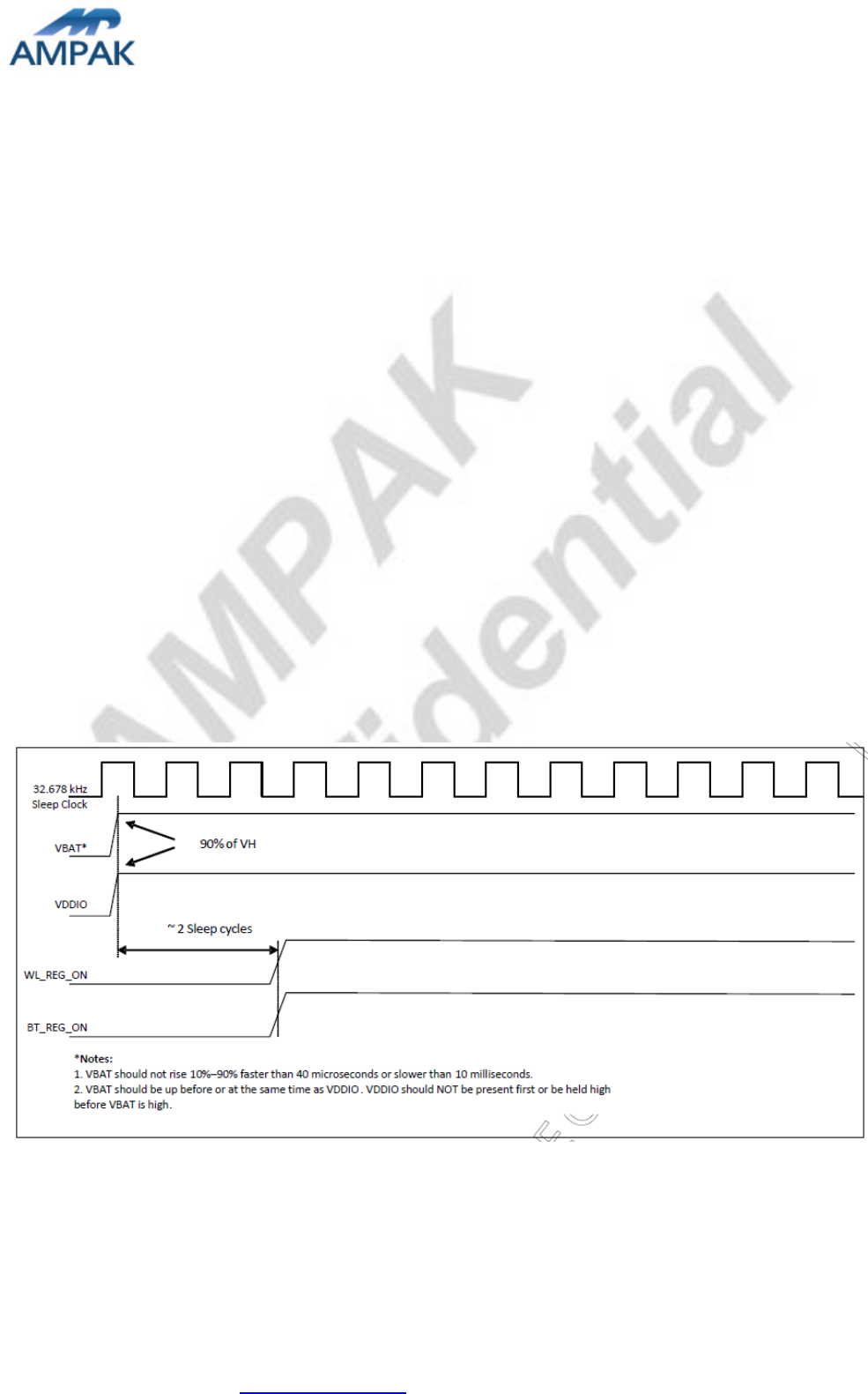
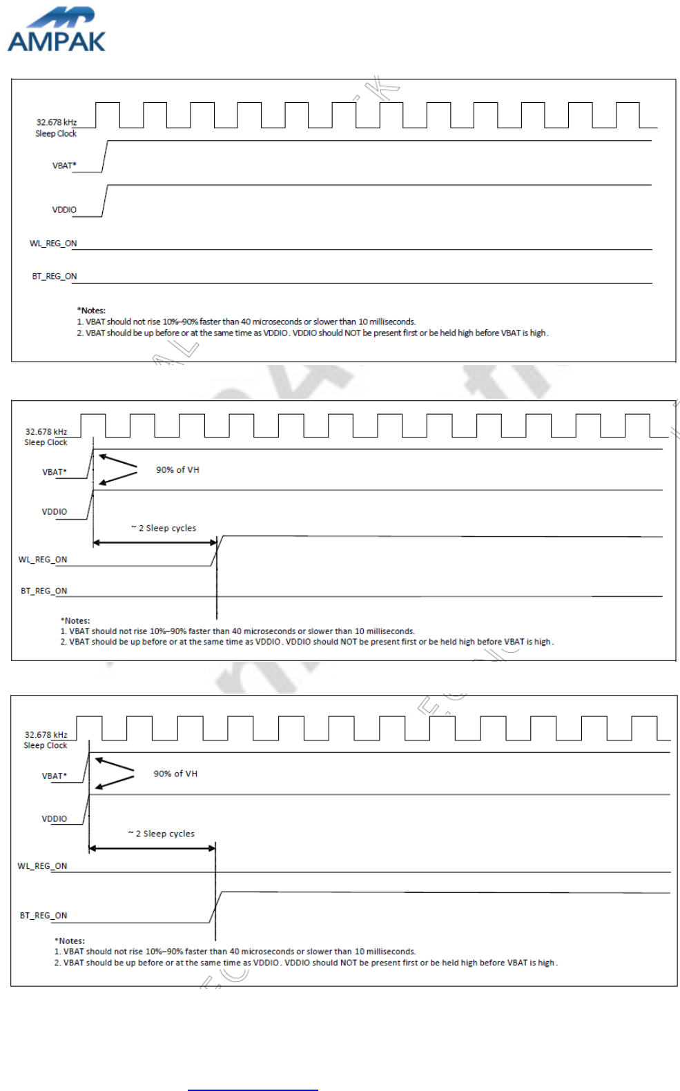
The module has signals that allow the host to control power consumption by enabling or
disabling the Bluetooth, WLAN and internal regulator blocks. These signals are described
below.
Additionally, diagrams are provided to indicate proper sequencing of the signals for carious
operating states. The timing value indicated are minimum required values: longer delays are
also acceptable.
※ WL_REG_ON: Used by the PMU to power up or power down the internal
regulators used by the WLAN section. When this pin is high, the regulators are
enabled and the WLAN section is out of reset. When this pin is low the WLAN
section is in reset.
※ BT_REG_ON: Used by the PMU to power up or power down the internal regulators
used by the BT section. Low asserting reset for Bluetooth. This pin has no effect on
WLAN and does not control any PMU functions. This pin must be driven high or low
(not left floating).
WLAN=ON, Bluetooth=ON
AP6255 Datasheet
AMPAK Technology Inc. www.ampak.com.tw Proprietary & Confidential Information
Doc. NO:
21
WLAN=OFF, Bluetooth=OFF
WLAN=ON, Bluetooth=OFF
WLAN=OFF, Bluetooth=ON
AP6255 Datasheet
AMPAK Technology Inc. www.ampak.com.tw Proprietary & Confidential Information
Doc. NO:
22
10.2 SDIO Default Mode Timing Diagram

AP6255 Datasheet
AMPAK Technology Inc. www.ampak.com.tw Proprietary & Confidential Information
Doc. NO:
23
10.3 SDIO High Speed Mode Timing Diagram
AP6255 Datasheet
AMPAK Technology Inc. www.ampak.com.tw Proprietary & Confidential Information
Doc. NO:
24
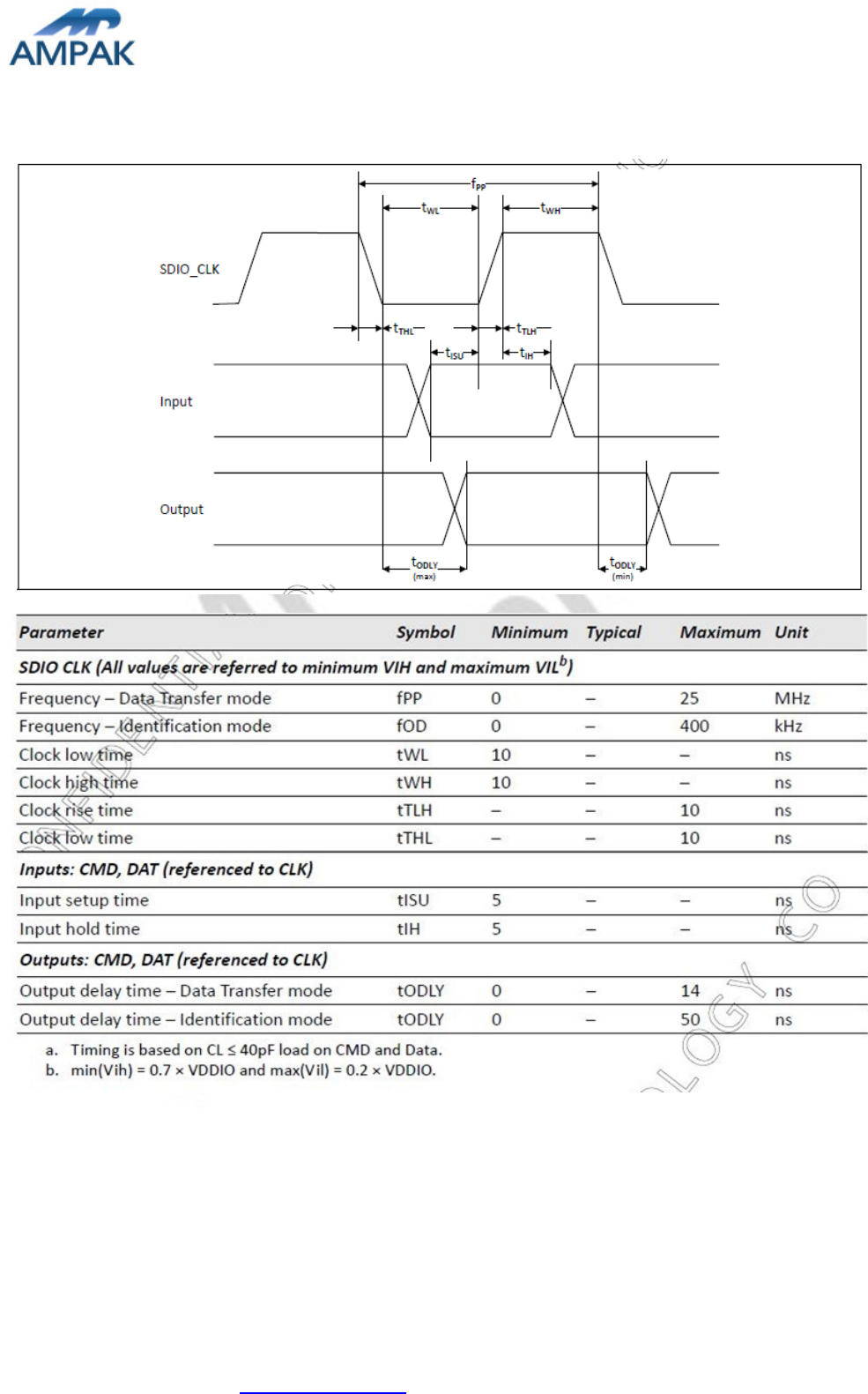
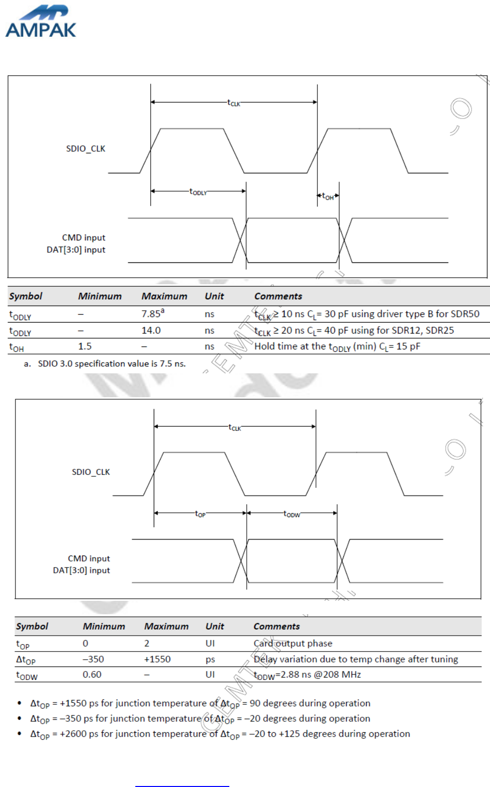
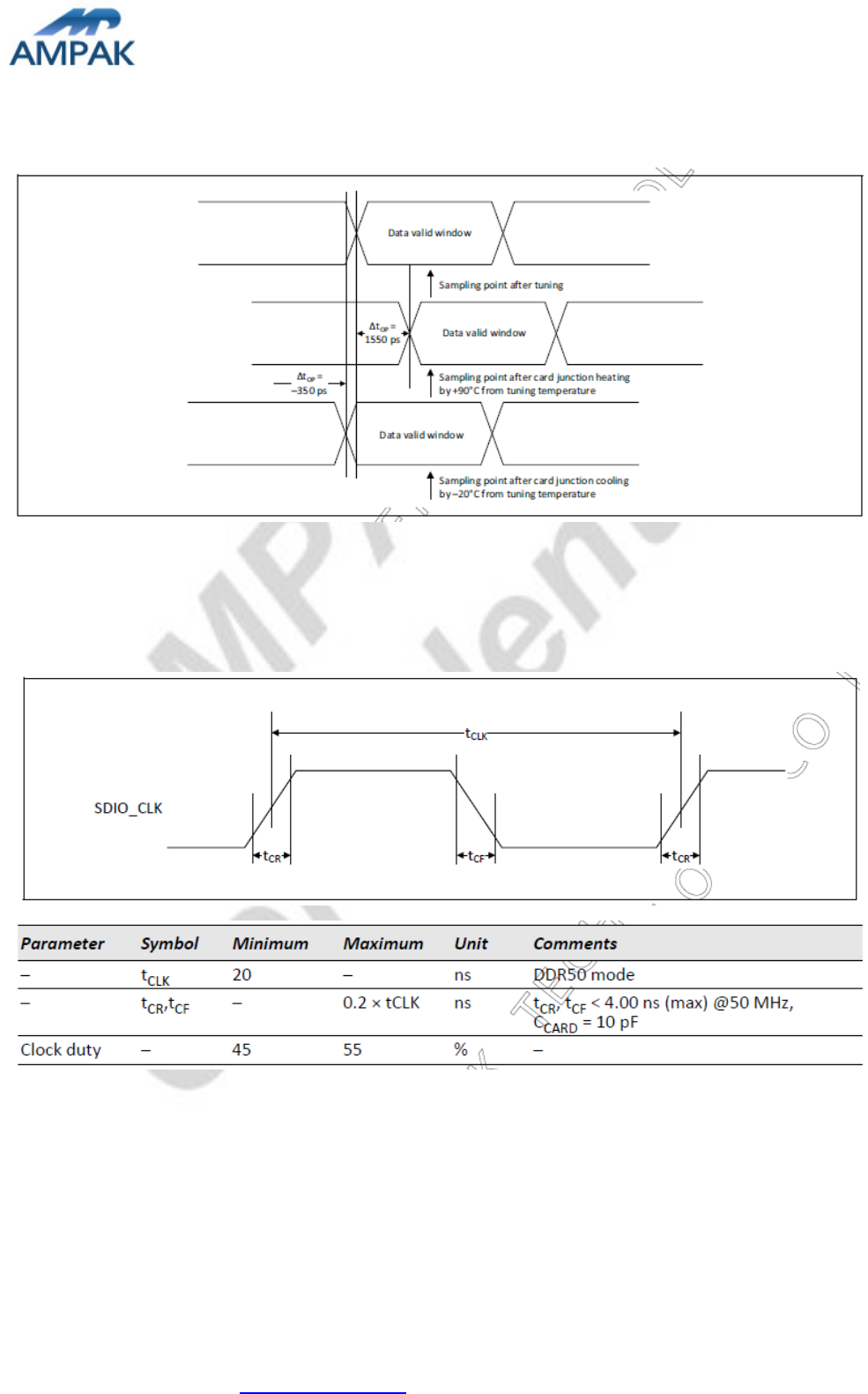
10.4 SDIO Bus Timing Specifications in SDR Modes
Clock timing (SDR Modes)
Card Input timing (SDR Modes)
AP6255 Datasheet
AMPAK Technology Inc. www.ampak.com.tw Proprietary & Confidential Information
Doc. NO:
25
Card output timing (SDR Modes up to 100MHz)
Card output timing (SDR Modes 100MHz to 208MHz)
AP6255 Datasheet
AMPAK Technology Inc. www.ampak.com.tw Proprietary & Confidential Information
Doc. NO:
26
OP
t∆Consideration for Variable Data Window (SDR 104 Mode)
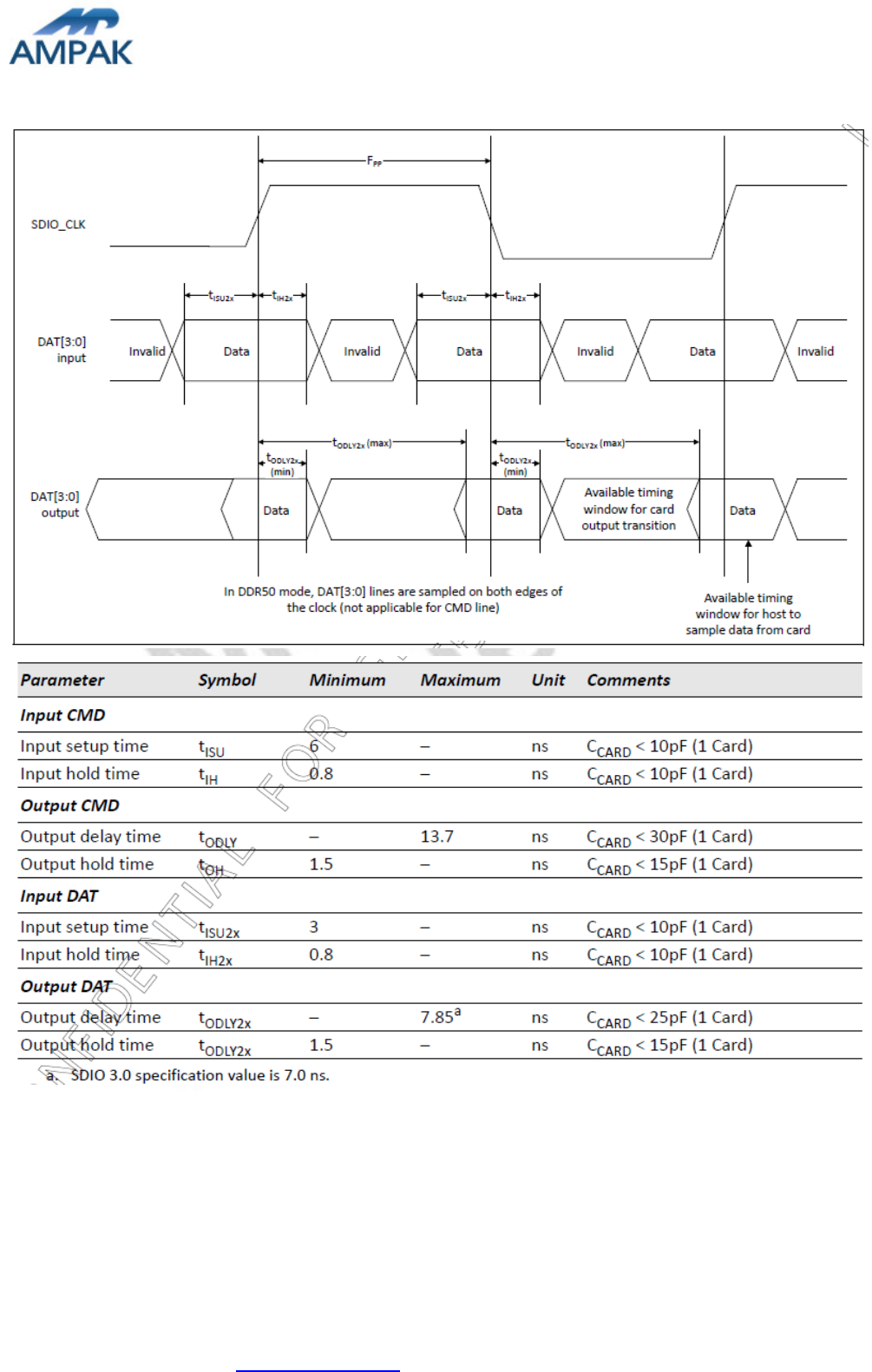
10.5 SDIO Bus Timing Specifications in DDR50 Mode
AP6255 Datasheet
AMPAK Technology Inc. www.ampak.com.tw Proprietary & Confidential Information
Doc. NO:
27
Data Timing
AP6255 Datasheet
AMPAK Technology Inc. www.ampak.com.tw Proprietary & Confidential Information
Doc. NO:
28
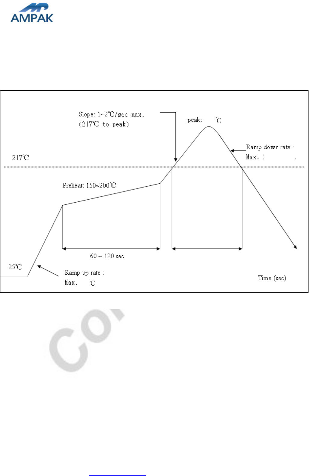
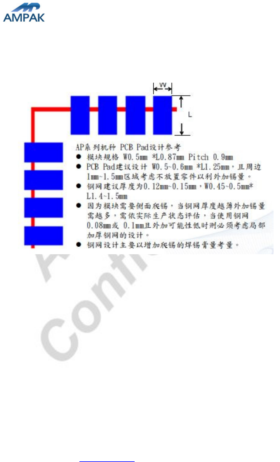
11. Recommended Reflow Profile
Referred to IPC/JEDEC standard.
Peak Temperature : <250°C
Number of Times : ≤2 times
2.
5 /sec
2.5
°
C
/sec
40~70 sec
2
50
AP6255 Datasheet
AMPAK Technology Inc. www.ampak.com.tw Proprietary & Confidential Information
Doc. NO:
29
Solder Paste definition
AP6255 Datasheet
AMPAK Technology Inc. www.ampak.com.tw Proprietary & Confidential Information
Doc. NO:
30
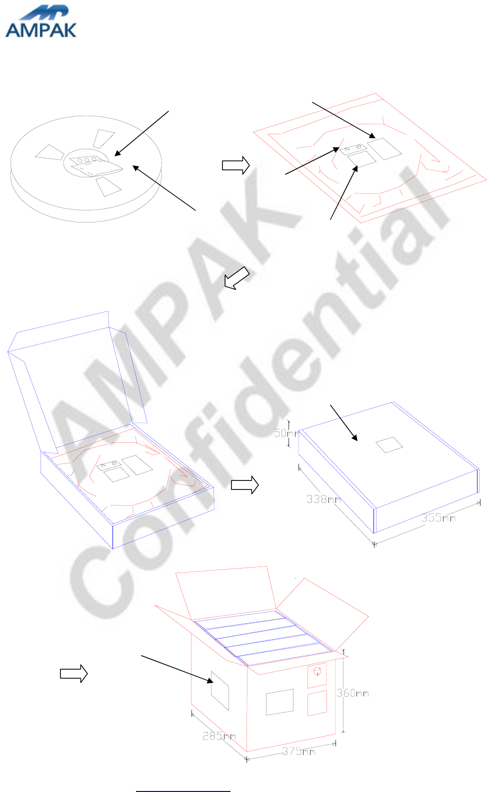
12. Package Information
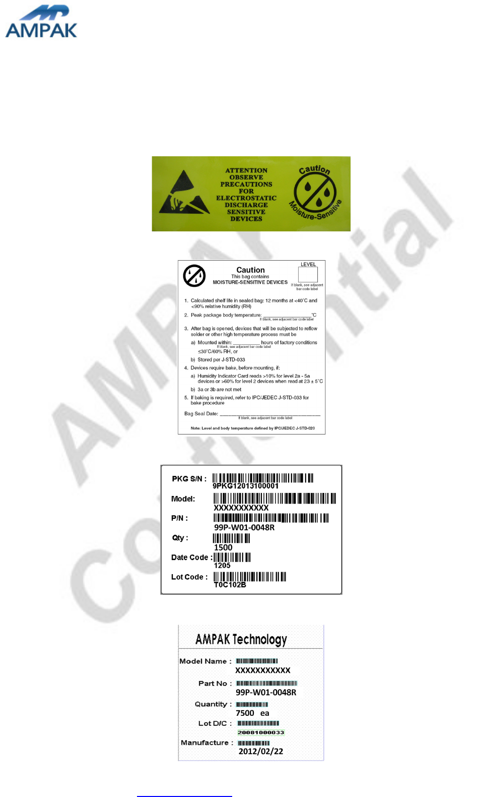
12.1 Label
Label A Anti-static and humidity notice
Label B MSL caution / Storage Condition
Label C Inner box label .
Label D Carton box label .
AP6255 Datasheet
AMPAK Technology Inc. www.ampak.com.tw Proprietary & Confidential Information
Doc. NO:
31
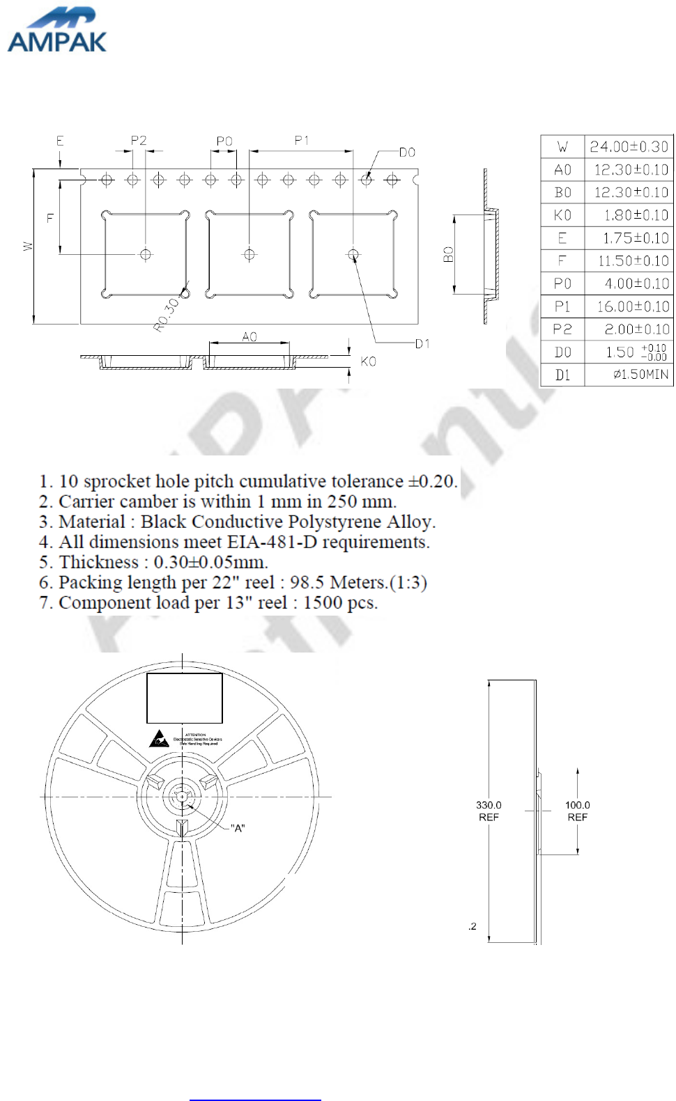
12.2 Dimension
AP6255 Datasheet
AMPAK Technology Inc. www.ampak.com.tw Proprietary & Confidential Information
Doc. NO:
32
A
B
C
Humidity indicator
Desiccant
C
D
AP6255 Datasheet
AMPAK Technology Inc. www.ampak.com.tw Proprietary & Confidential Information
Doc. NO:
33
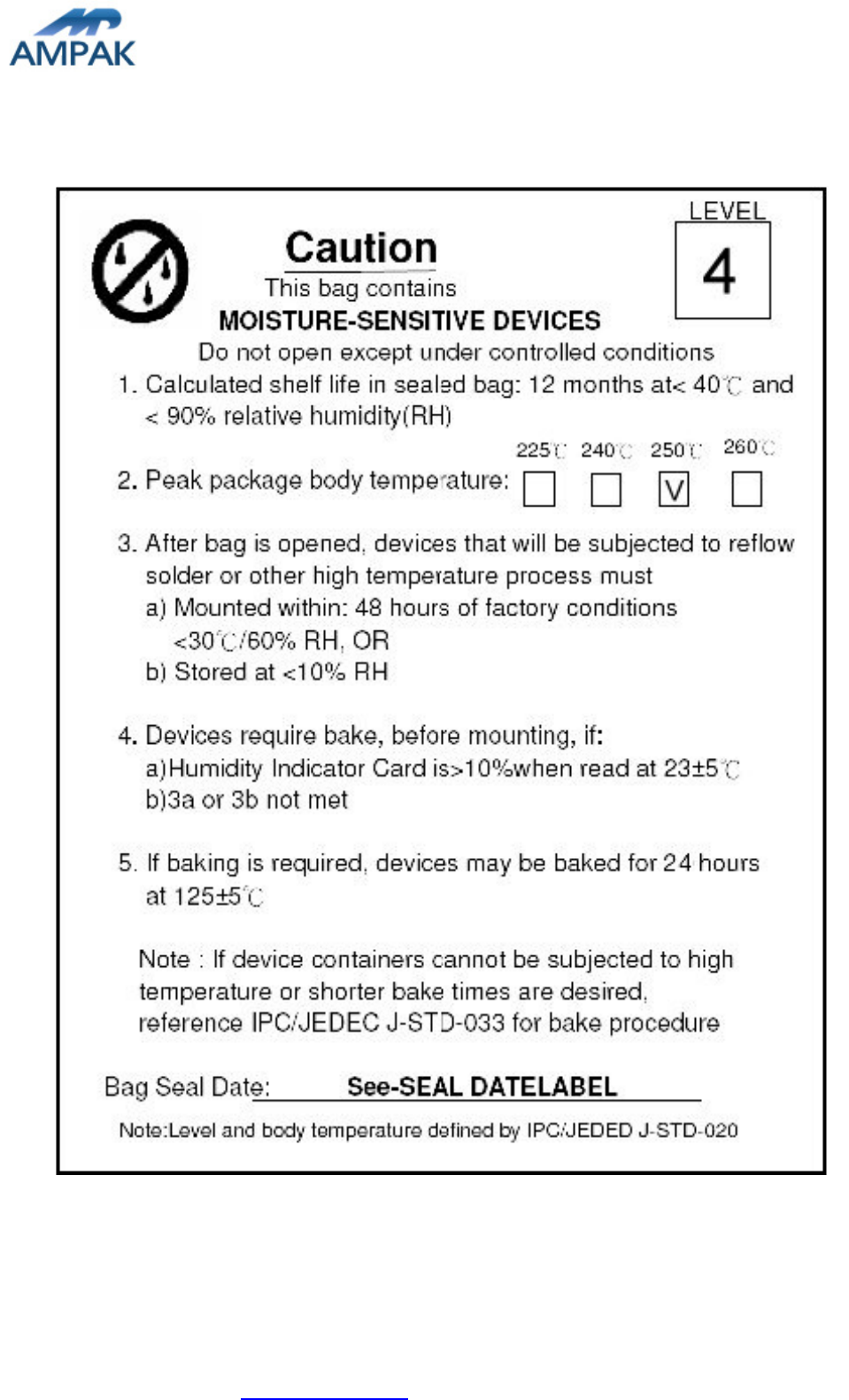
12.3 MSL Level / Storage Condition
※
※※
※NOTE : Accumulated baking time should not exceed 96hrs
Federal Communication Commission Interference Statement
This equipment has been tested and found to comply with the limits for a Class B digital device, pursuant to Part 15 of the FCC Rules. These limits are
designed to provide reasonable protection against harmful interference in a residential installation. This equipment generates, uses and can radiate radio
frequency energy and, if not installed and used in accordance with the instructions, may cause harmful interference to radio communications. However,
there is no guarantee that interference will not occur in a particular installation. If this equipment does cause harmful interference to radio or television
reception, which can be determined by turning the equipment off and on, the user is encouraged to try to correct the interference by one of the following
measures:
- Reorient or relocate the receiving antenna.
- Increase the separation between the equipment and receiver.
- Connect the equipment into an outlet on a circuit different from that to which the receiver is connected.
- Consult the dealer or an experienced radio/TV technician for help.
FCC Caution:
Any changes or modifications not expressly approved by the party responsible for compliance could void the user's authority to operate this equipment.
This device complies with Part 15 of the FCC Rules. Operation is subject to the following two conditions:
(1) This device may not cause harmful interference, and
(2) This device must accept any interference received, including interference that may cause undesired operation.
FCC Radiation Exposure Statement:
This equipment complies with FCC radiation exposure limits set forth for an uncontrolled environment. This transmitter module must not be co-located
or operating in conjunction with any other antenna or transmitter.
This End equipment should be installed and operated with a minimum distance of 20 centimeters between the radiator and your body.
IMPORTANT NOTE:
In the event that these conditions cannot be met (for example certain laptop configurations or co-location with another transmitter), then the FCC
authorization is no longer considered valid and the FCC ID cannot be used on the final product. In these circumstances, the OEM integrator will be
responsible for re-evaluating the end product (including the transmitter) and obtaining a separate FCC authorization.
End Product Labeling
The final end product must be labeled in a visible area with the following:
“Contains FCC ID: 2AFG6-RK3399”.
Manual Information to the End User
The OEM integrator has to be aware not to provide information to the end user regarding how to install or remove this RF module in the user’s manual
of the end product which integrates this module.
Canada Statement
This device complies with Industry Canada’s licence-exempt RSSs. Operation is subject to the following two conditions:
(1) This device may not cause interference; and
(2) This device must accept any interference, including interference that may cause undesired operation of the device.
Le présent appareil est conforme aux CNR d’Industrie Canada applicables aux appareils radio exempts de licence. L’exploitation est autorisée aux deux
conditions suivantes :
(1) l’appareil ne doit pas produire de brouillage;
(2) l’utilisateur de l’appareil doit accepter tout brouillage radioélectrique subi, même si le brouillage est susceptible d’en compromettre le
fonctionnement.
Caution Exposure:
This device meets the exemption from the routine evaluation limits in section 2.5 of RSS102 and users can obtain Canadian information on RF exposure
and compliance.
Le dispositif répond à l'exemption des limites d'évaluation de routine dans la section 2.5 de RSS102 et les utilisateurs peuvent obtenir des
renseignements canadiens sur l'exposition aux RF et le respect.
the device for operation in the band 5150-5250 MHz is only for indoor use to reduce the potential for harmful interference to co-channel mobile satellite
systems
les dispositifs fonctionnant dans la bande 5150-5250 MHz sont réservés uniquement pour une utilisation à l’intérieur afin de réduire les risques de
brouillage préjudiciable aux systèmes de satellites mobiles utilisant les mêmes canaux;
Users should also be advised that high-power radars are allocated as primary users (i.e. priority users) of the bands 5250-5350 MHz and 5650-5850 MHz
and that these radars could cause interference and/or damage to LE-LAN devices.
les utilisateurs de radars de haute puissance sont désignés utilisateurs principaux (c.-à-d., qu'ils ont la priorité) des bandes de 5 250 à 5 350 MHz et de 5
650 à 5 850 MHz et, d’autre part, que ces radars pourraient causer du brouillage et/ou des dommages aux dispositifs de RL-EL.
for devices with detachable antenna(s), the maximum antenna gain permitted for devices in the band 5725-5850 MHz shall be such that the equipment
still complies with the e.i.r.p. limits specified for point-to-point and non-point-to-point operation as appropriate.

le gain maximal d’antenne permis (pour les dispositifs utilisant la bande 5 725-5 825 MHz) doit se conformer à la limite de p.i.r.e. spécifiée pour
l’exploitation point à point et non point à point, selon le cas.
The final end product must be labelled in a visible area with the following:
The Industry Canada certification label of a module shall be clearly visible at all times when installed in the host device, otherwise the host device must
be labelled to display the Industry Canada certification number of the module, preceded by the words “Contains transmitter module”, or the word
“Contains”, or similar wording expressing the same meaning, as follows:
Contains transmitter module IC: 22166-RK3399
The module must be installed in Android Module
This End equipment should be installed and operated with a minimum distance of 20 centimeters between the radiator and your body.
Cet équipement devrait être installé et actionné avec une distance minimum de 20 centimètres entre le radiateur et votre corps.
The end user manual shall include all required regulatory information/warning as show in this manual.
This radio transmitter (RK3399) has been approved by Industry Canada to operate with the antenna types listed below with the maximum permissible
gain and required antenna impedance for each antenna type indicated. Antenna types not included in this list, having a gain greater than the maximum
gain indicated for that type, are strictly prohibited for use with this device.
Le présent émetteur radio (RK3399) a été approuvé par Industrie Canada pour fonctionner avec les types d'antenne énumérés ci-dessous et ayant un gain
admissible maximal et l'impédance requise pour chaque type d'antenne. Les types d'antenne non inclus dans cette liste, ou dont le gain est supérieur au
gain maximal indiqué, sont strictement interdits pour l'exploitation de l'émetteur.
2.4G:
5G: