HB Wireless Communication Technology CG757560 RF module User Manual S200 SPEC
HB Wireless Communication Technology RF module S200 SPEC
Users Manual

1
HongBo
HM7601 SIP Module
User Manual
Product
Version
Date

2
Document History
Date
Revised Contents
Revised by
Version
Oct. 18th,2015
Preliminary version
Derrick
1.0

3
INDEX
1. Description ................................................................................................................................................. 4
1-1. Block Diagram ....................................................................................................................................... 5
1-2. Specification .......................................................................................................................................... 6
2. Electrical Characteristics ............................................................................................................................ 7
2-1. Absolute Maximum Ratings ................................................................................................................. 7
2-2. Recommended Operation Conditions ................................................................................................. 7
2-3. Current consumption ............................................................................................................................ 7
2-4. RF Characteristics .................................................................................................................................. 8
2-4-1. RF Tx Specification ........................................................................................................................... 8
2-4-2. RF Rx Specification ......................................................................................................................... 10
2-5. SDIO Host Interface Protocol Timing ......................................................................................................
2-5-1. SDIO 25MHz Timing Waveform ..........................................................................................................
2-5-2. SDIO 50MHz Timing Waveform ..........................................................................................................
3. Pin Definition ........................................................................................................................................... 11
3-1. Pin Description ...................................................................................................................................... 11
3-2. Pin Assignment ..................................................................................................................................... 11
3-3. Mechanical Dimensions ....................................................................................................................... 12
4. Regulation ................................................................................................................................................ 13
5. Recommended Reflow Profile ................................................................................................................ 13
6. SiP Module Preparation .......................................................................................................................... 14
6-1. Handling .............................................................................................................................................. 14
6-2. SMT Preparation ................................................................................................................................. 14
7. Package Information ............................................................................................................................... 15
7-1. Product Making ................................................................................................................................... 15
7-2. Tray Dimension ........................................................................................................................................
7-3. Packing Information............................................................................................................................ 16
7-4. Humidity Indicator Card ..................................................................................................................... 17

4
1. Description
HM7601 is a low-cost Wi-Fi SIP module, which fully supports the features and functional compliance of IEEE
802.11b/g/n standards. It supports up to 150Mbps high-speed wireless network connections. Also, it is
designed to provide excellent performance with low power consumption as well as a cost-effective solution.
The module is able to be developed for Wi-Fi USB dongle, Wi-Fi camera, wireless module for IoT products..etc.
Feature
Small dimension : 11mm X 11mm X 2.0mm
Host interface : USB 2.0
Support Orthogonal Frequency Division Multiplexing(OFDM), Complementary Code Keying(CCK), and Direct
Sequence Spread Spectrum(DSSS) to provide a variety of data rates
Integrated switching regulator enables direct connection to battery
Support AP /STA / ad-hoc mode / Wi-Fi direct
IEEE 802.11n (HT20 MCS7), IEEE 802.11g(OFDM 54Mbps) and IEEE 802.11b(DSSS 11Mbps)
Support Wi-Fi Direct (WFA P-2-P Standard)
Security: WFA WPA/WPA2 personal, WPS2.0, WAPI
QoS: WFA WMM, WMM PS
Compatible with Windows XP, Vista, W7 32/64, W8 32/64, W8.1 32/64
Linux and MAC OS X
Plug and play, easy set-up installation
5
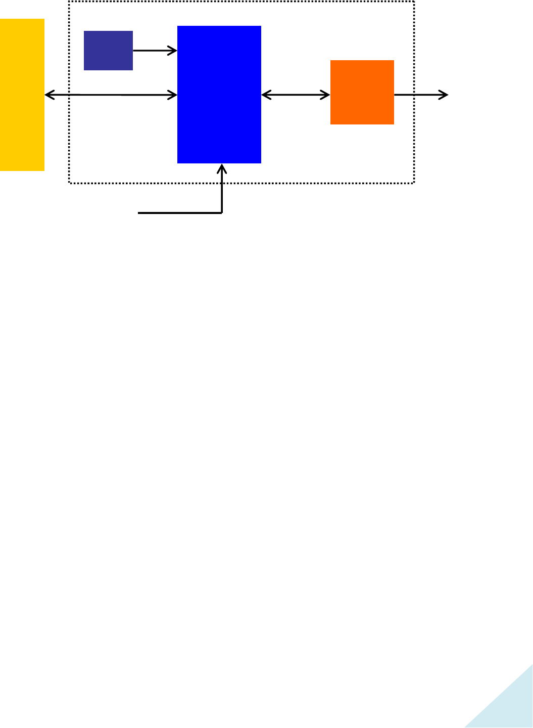
1-1. Block Diagram
A simplified block diagram of the HM7601 SiP module is shown in the figure below.
MT7601
Balun
Filter
WL/2.4G/TRx
Crystal
40MHz
USB Interface
Interface Signals
External 3.3V
ANT
AI7601H

6
1-2. Specification
Model Name
HM7601
Product Description
Wi-Fi SiP Module
Network Standard
IEEE 802.11b/g/n Compliant
Host Interface
USB 2.0
Operation Conditions
Operating Voltage
3.3V typ.
Temperature
Operating : 0℃ ~ 70℃
Storage : -40℃ ~ 125℃
Humidity
Operating : 10 ~ 95% (Non-Condensing)
Storage : 5 ~ 95% (Non-Condensing)
Dimension
11mm X 11mm X 2.0mm
Package
Half hole stamp type
Electrical Specifications
Frequency
2.4GHz ISM radio band
Channel
1~14
Modulation
DSSS, OFDM, 64-QAM, 16-QAM, QPSK, BPSK, CCK, DQPSK, DBPSK
Security
WFA WPA/WPA2 personal
WPS2.0
WAPI
Operation System
Windows XP, Vista, W7 32/64, W8 32/64, W8.1 32/64 ; Linux and MAC
OS X

7
2. Electrical Characteristics
2-1. Absolute Maximum Ratings
Symbol
Parameter
Min.
Max.
Unit
VDD33
Power supply
-0.3
3.6
V
2-2. Recommended Operation Conditions
Symbol
Parameter
Min.
Typ.
Max.
Unit
VDD33
Power supply
2.97
3.3
3.63
V
2-3. Current consumption
Description
Performance
Typ.
Units
Sleep mode
1.1
μA
RX Active, BW40, MCS7
151
mA
RX Listen
6
mA
RX Power saving, DTIM=1
15
mA
TX HT40, MCS7@15dBm
210
mA
TX CCK, 11M@19dBm
242
mA
Note: All result is measured at the antenna port and VDD33 is 3.3V.

8
2-4. RF Characteristics
2-4-1. RF Tx Specification (@module O/P)
802.11b Transmit
Item
Condition
Min.
Typ.
Max.
Unit
Frequency range
Channel 1
Channel 14
Tx Power Level
1~11Mbps DSSS
16
18
20
dBm
Frequency tolerance
-10
10
ppm
Spectral Mask
11MHz→22MHz
-30
dBr
>22MHz
-50
dBr
Tx power-on
10%→90%
0.2
2
uS
Tx power-down
90%→10%
0.2
2
uS
Modulation accuracy
1/2/5.5/11 Mbps
4
8
20
%
802.11g Transmit
Item
Condition
Min.
Typ.
Max.
Unit
Frequency range
Channel 1
Channel 14
Tx Power Level
6~54Mbps OFDM
14
16
18
dBm
Frequency tolerance
-10
10
ppm
Modulation accuracy
54Mbps
<-30
-25
dB
48 Mbps
<-30
-22
dB
36 Mbps
<-30
-19
dB
24 Mbps
<-30
-16
dB
18 Mbps
<-30
-13
dB
12 Mbps
<-30
-10
dB
9 Mbps
<-30
-8
dB
6 Mbps
<-30
-5
dB
Spectral Mask
11MHz
-20
dBr
20MHz
-28
dBr
30MHz
-40
dBr
Spectral flatness
±10 sub-carrier
-2
2
dB
±17→±26 sub-carrier
-4
2
dB

9
802.11n Transmit
Item
Condition
Min.
Typ.
Max.
Unit
Frequency range
Channel 1
Channel 14
Tx Power Level
HT20 MCS0~7
13
15
17
dBm
Frequency tolerance
-10
10
ppm
Modulation accuracy
MCS 7
<-30
-28
dB
MCS 6
<-30
-25
dB
MCS 5
<-30
-22
dB
MCS 4
<-30
-19
dB
MCS 3
<-30
-16
dB
MCS 2
<-30
-13
dB
MCS 1
<-30
-10
dB
MCS 0
<-30
-5
dB
Spectral Mask
11MHz
-20
dBr
20MHz
-28
dBr
30MHz
-45
dBr
Spectral flatness
±10 sub-carrier
-2
2
dB
±17→±28 sub-carrier
-4
2
dB

10
2-4-2. RF Rx Specification (@module O/P)
802.11b Receiver
Item
Condition
Min.
Typ.
Max.
Unit
Frequency range
Channel 1
Channel 14
Min. input
(PER<8%)
11Mbps
-84
-76
dBm
5.5Mbps
-87
-76
dBm
2Mbps
-89
-80
dBm
1Mbps
-92
-80
dBm
Max. input level
11Mbps
0
dBm
802.11g Receiver
Item
Condition
Min.
Typ.
Max.
Unit
Frequency range
Channel 1
Channel 14
Min. input
(PER<10%)
54Mbps
-71
-65
dBm
48Mbps
-72
-66
dBm
36Mbps
-77
-70
dBm
24Mbps
-80
-74
dBm
18Mbps
-83
-77
dBm
12Mbps
-85
-79
dBm
9Mbps
-87
-81
dBm
6Mbps
-88
-82
dBm
Max. input level
6/54Mbps
0/-10
dBm
802.11n HT20 Receiver
Item
Condition
Min.
Typ.
Max.
Unit
Frequency range
Channel 1
Channel 14
Min. input
(PER<10%)
MCS 7
-70
-64
dBm
MCS 6
-71
-65
dBm
MCS 5
-73
-66
dBm
MCS 4
-77
-70
dBm
MCS 3
-80
-74
dBm
MCS 2
-83
-77
dBm
MCS 1
-85
-79
dBm
MCS 0
-87
-82
dBm
Max. input level
MCS0/MCS7
-10/-14
dBm

11
3. Pin Definition
3-1. Pin Description
Pin
Definition
I/O
Description
1
VDD33
Power
Main power supply
2
GND
Power
Ground
3
DP
AIO
D+ data input/output
4
DM
AIO
D- data input/output
5
WL_GPIO5
DIO
LED indicator control signal
6
WL_GPIO2
DIO
WPS button control signal
7
GND
Power
Ground
8
ANT_Module
RF
2.4GHz RF output
9
GND
Power
Ground
12
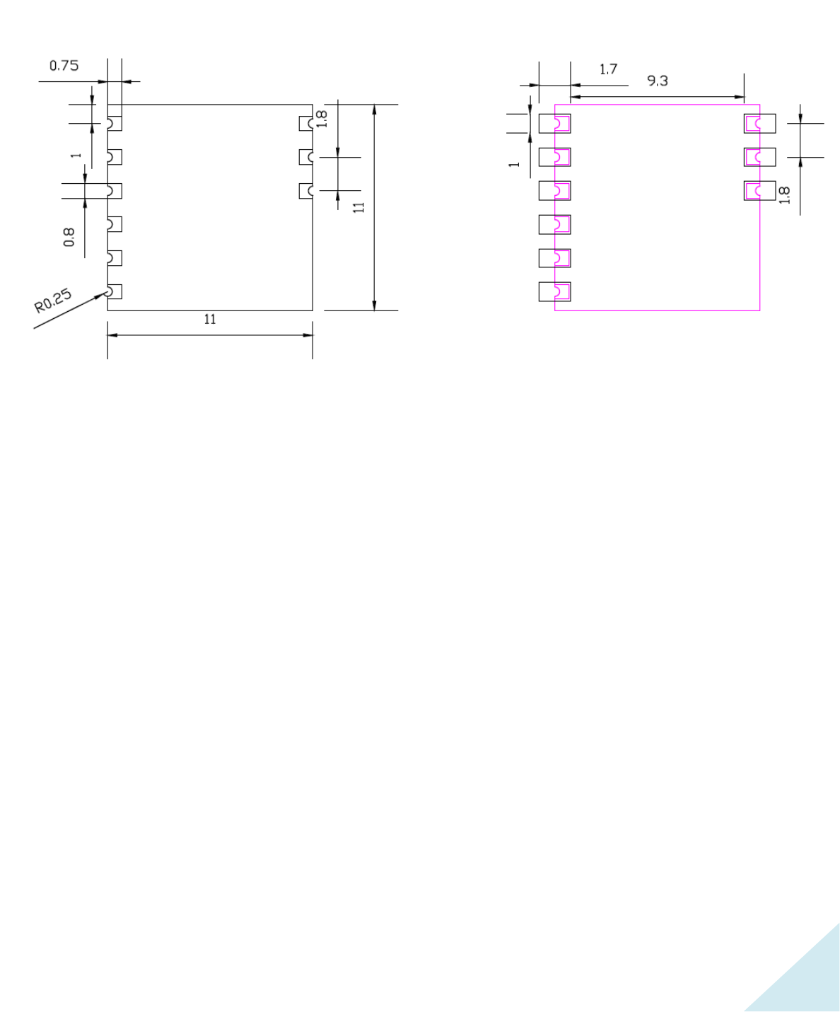
3-2. Pin Assignment and Mechanical Dimensions
The SiP module will conform to the following pin map, shown in the following diagram (top view)
UNIT: mm
Pin1 Pin9
TOP View
13
4. Regulation
The SiP module was pre-scanned with module level to comply with following standards:
• US/CAN: FCC CFR47 Part 15.247
• Europe: ETS 300-328 V1.6.1
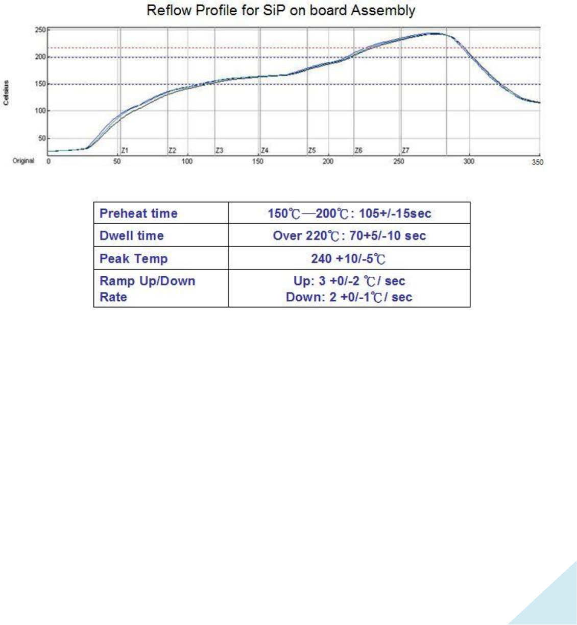
5. Recommended Reflow Profile

14
6. SiP Module Preparation
6-1. Handling
Handling the module must wear the anti-static wrist strap to avoid ESD damage. After each module is aligned
and tested, it should be transport and storage with anti -static tray and packing. This protective package must
be remained in suitable environment until the module is assembled and soldered onto the main board.
6-2. SMT Preparation
1. Calculated shelf life in sealed bag: 6 months at<40℃ and <90% relative humidity (RH).
2. Peak package body temperature: 250℃.
3. After bag was opened, devices that will be subjected to reflow solder or other high temperature process
must.
A. Mounted within: 168 hours of factory conditions<30℃/60%RH.
B. Stored at≦10%RH with N2 flow box.
4. Devices require baking, before mounting, if:
A. Package bag does not keep in vacuumed while first time open.
B. Humidity Indicator Card is >10% when read at 23±5℃.
C. Expose at 3A condition over 8 hours or Expose at 3B condition over 24 hours.
5. If baking is required, devices may be baked for 12 hours at 125±5℃.

15
7. Federal Communications Commission (FCC) Statement
This device complies with Part 15 of the FCC Rules. Operation is subject to the following two conditions: (1)
This device may not cause harmful interference, and (2) this device must accept any interference received,
including interference that may cause undesired operation.
This equipment has been tested and found to comply with the limits for a Class B digital device, pursuant to
Part 15 of the FCC Rules. These limits are designed to provide reasonable protection against harmful
interference in a residential installation. This equipment generates, uses and can radiate radio frequency
energy and, if not installed and used in accordance with the instructions, may cause harmful interference to
radio communications. However, there is no guarantee that interference will not occur in a particular
installation. If this equipment does cause harmful interference to radio or television reception, which can
be determined by turning the equipment off and on, the user is encouraged to try to correct the interference
by one of the following measures:
Reorient or relocate the receiving antenna.
Increase the separation between the equipment and receiver.
Connect the equipment into an outlet on a circuit different from that
to which the receiver is connected.
Consult the dealer or an experienced radio/TV technician for help.
This device complies with Part 15 of the FCC Rules. Operation is subject to the following two conditions:
1) this device may not cause harmful interference and
2) this device must accept any interference received, including interference that may cause undesired
operation of the device.
FCC RF Radiation Exposure Statement:
1. This Transmitter must not be co-located or operating in conjunction with any other antenna or

16
transmitter.
2. This equipment complies with FCC RF radiation exposure limits set forth for an uncontrolled environment.
This equipment should be installed and operated with a minimum distance of 20 centimeters between
the radiator and your body.
End Product Labeling:
This module is designed to comply with the FCC statement, FCC ID :2AJICCG757560
The host system using this module, should have label in a visible area indicated the following texts:
"Contains FCC ID :2AJICCG757560".
Manual Information to the End User
The OEM integrator has to be aware not to provide information to the end user regarding how to install or
remove this RF module in the user’s manual of the ed product which integrates this module.
The end user manual shall include all required regulatory information/warning as shown in this manual.