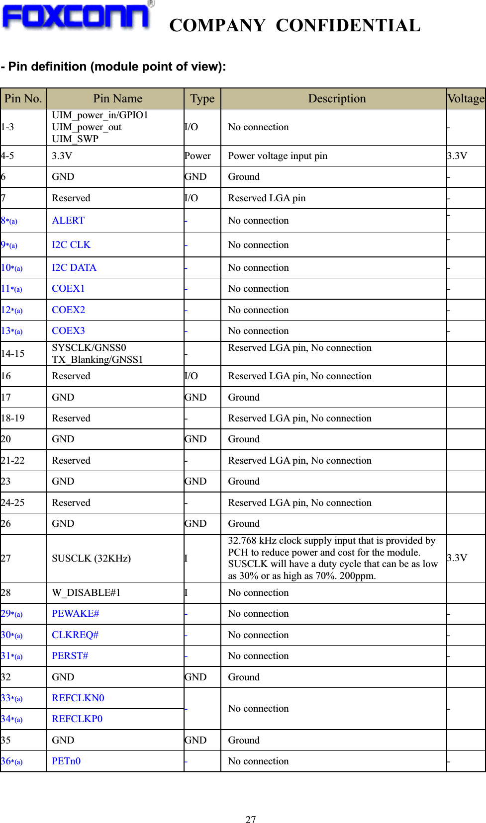
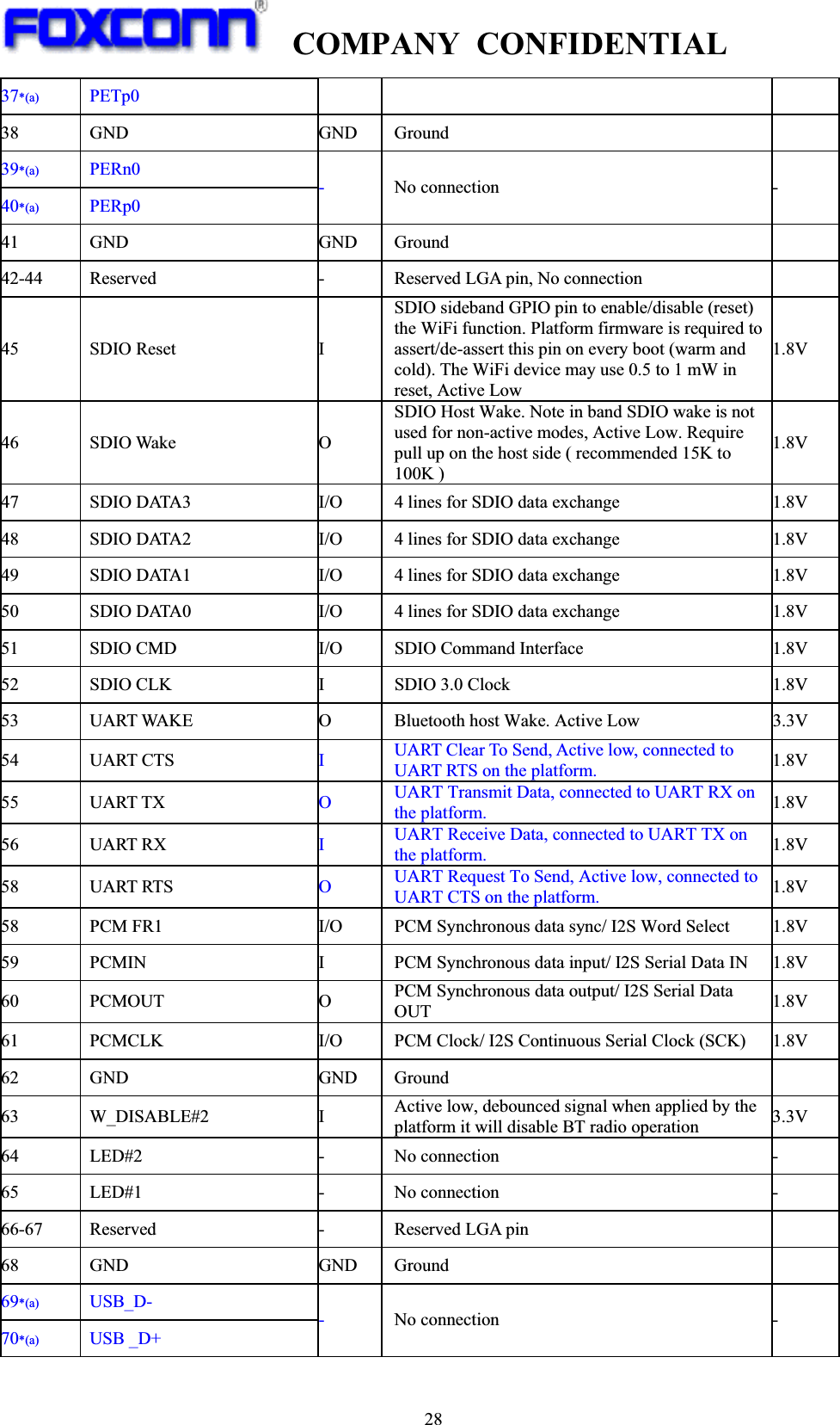
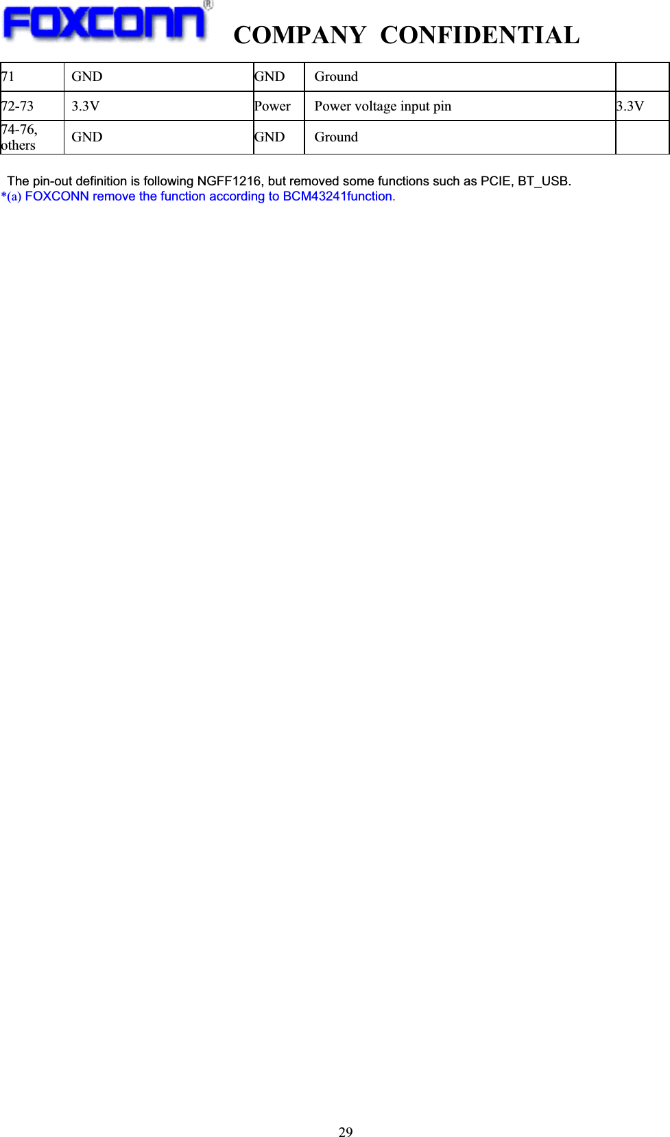
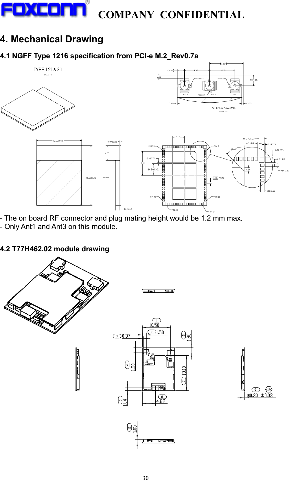
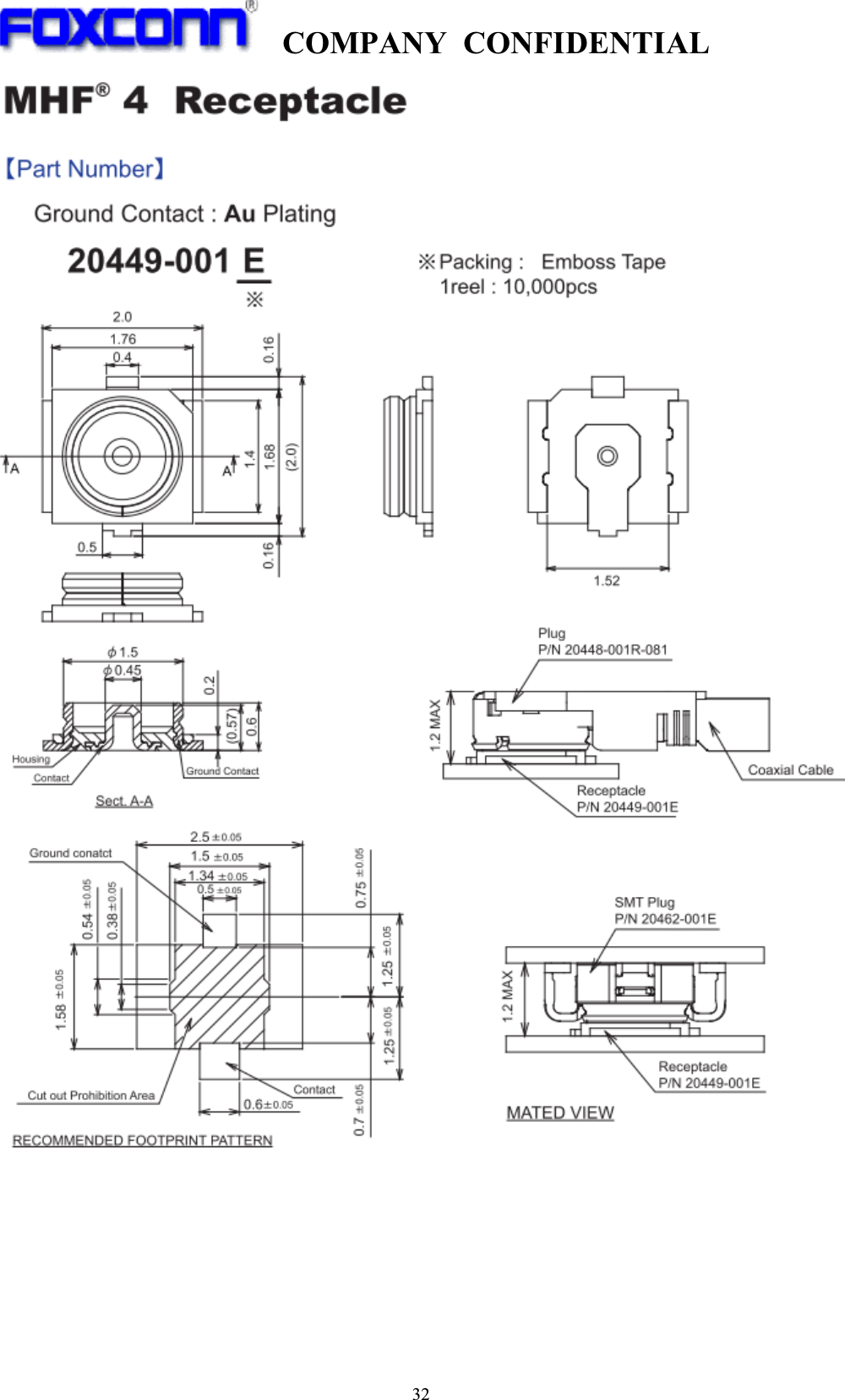
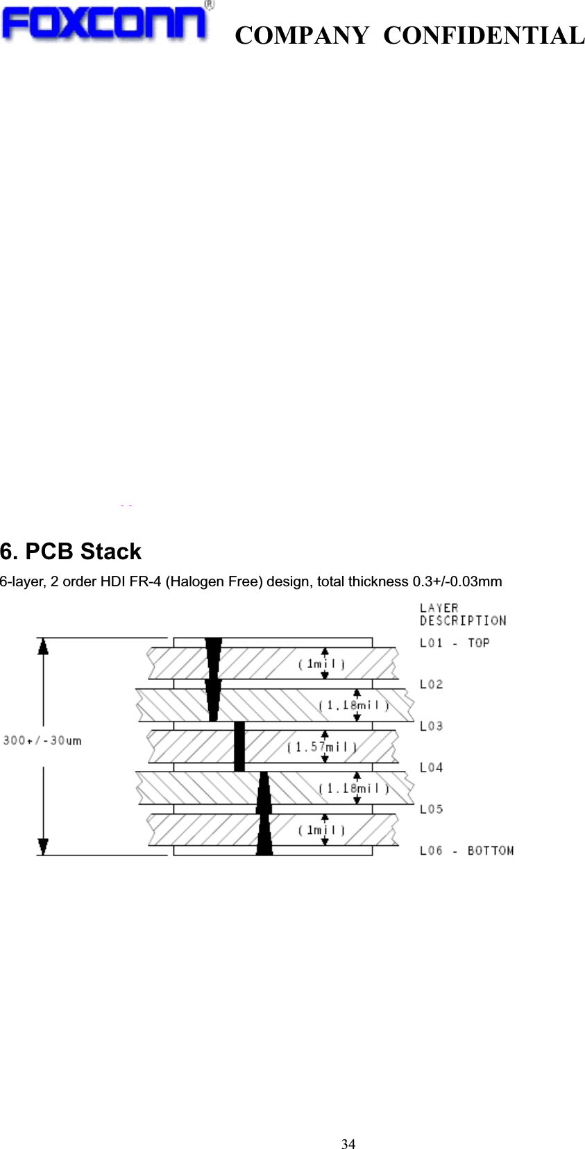
HON HAI PRECISION IND T77H462 802.11abgn+BT4.0 module User Manual

HON HAI Precision Ind. Co., Ltd. 802.11abgn+BT4.0 module

User Manual.pdf

COMPANY CONFIDENTIAL1!Prepared by  Reviewed by  Approved by Jason Hu  Gary Su  Chang-fu Lin !TotalPages ProductRev. Date Sales39 01S1 20130725 EagleWeiPartName 802.11a/g/n+BT4.0ModuleRevisionNoteRev. 3.2FoxconnPartNo. T77H462.02LenovoPartNo.HONHAIPRECISIONIND.CO.,LTD.5F1,5HsinAnRoad,Hsinchu,ScienceBasedIndustrialPark300,TaiwanTel:+88635784975 Revision Note (Specification Sheet)
COMPANY CONFIDENTIAL2!           Index 1. REVISION HISTORY ................................................................................................................................................... 32. INTRODUCTION .......................................................................................................................................................... 42.1 SCOPE ...................................................................................................................................................................... 42.2 FUNCTION ................................................................................................................................................................. 43. PRODUCT SPECIFICATION ..................................................................................................................................... 53.1 HARDWARE CHARACTERISTIC ................................................................................................................................. 53.2 HARDWARE ARCHITECTURE .................................................................................................................................... 53.3 ELECTRICAL SPECIFICATION .................................................................................................................................... 63.4 WLAN RF CHARACTERISTICS ................................................................................................................................. 73.4.1 IEEE802.11b .................................................................................................................................................. 73.4.2 IEEE802.11g .................................................................................................................................................. 83.4.4 IEEE802.11a ................................................................................................................................................ 123.5 BLUETOOTH RF SPECIFICATIONS .......................................................................................................................... 183.6 INTERFACE TIMING .................................................................................................................................................. 233.6.1 SDIO INTERFACE TIMING .................................................................................................................................... 233.6.2 UART INTERFACE TIMING ................................................................................................................................... 253.7 LGA PIN DEFINITION .............................................................................................................................................. 264. MECHANICAL DRAWING ....................................................................................................................................... 305. SCHEMATIC REFERENCE DESIGN ..................................................................................................................... 336. PCB STACK ............................................................................................................................................................... 347. SOFTWARE SUPPORT ............................................................................................................................................ 358. REGULATORY ........................................................................................................................................................... 369. ENVIRONMENTAL REQUIREMENTS AND SPECIFICATIONS ....................................................................... 379.1 TEMPERATURE ....................................................................................................................................................... 379.2 PCB BENDING ........................................................................................................................................................ 379.3 HANDLING ENVIRONMENT ....................................................................................................................................... 379.4 STORAGE CONDITION ............................................................................................................................................. 379.5 BAKING CONDITION ................................................................................................................................................ 379.6 SOLDERING AND REFLOW CONDITION .................................................................................................................... 3810 PACKAGE INFORMATION ..................................................................................................................................... 39
COMPANY CONFIDENTIAL3!1. Revision History  Date Change Note  Rev. 2012-12-26 Initial release  1.0 2013-01-18  Modify the Pin definition to PCIeM.2_Rev0.7a and RF connector information  1.1 2013-04-08 Modify  Section 3.2: Hardware Architecture Section 3.4: WLAN RF Characteristics Section 3.6: LGA Pin Definition: add note to some pins Chapter 4: add note to the mechanical drawing   2.0 2013-04-12 Modify  Section 3.2: Hardware Architecture Section 3.4: WLAN RF Characteristics Section 3.6: LGA Pin Definition Section 5: Schematics reference design 2.1 2013-04-26 Add Section 3.6: signal level voltage Modify  Section 3.6: UART_WAKE from platform signal Output to Signal Input  2.2 2013-06-28 Modify Section 3.4: WLAN RF Characteristics Section 3.5: BT RF Characteristics   Add 3.6 interface timing Section 3.7: Pin definition Section 4: Mechanical drawing Section 5: schematics reference design Section 7: Software support Section 8: Regulatory Section 9: environment specification Section 10: package information3.0 2013-07-02  Modify Section 3.7: Pin definition, The I/O type of UART pin 54-58    3.1 2013-07-25  Add FCC power table  3.2
COMPANY CONFIDENTIAL4!2. Introduction Project Name: 802.11abgn (2X2) + BT4.0 combo module This documentation describes the product specification of the WLAN+BT combo Module. WLAN is Compliant with IEEE 802.11 a/b/g and 2x2 IEEE 802.11n MAC/ baseband/radio, Bluetooth is compliant with Bluetooth 4.0+HS. This module takes advantage of the high throughput and extended range of Broadcom second-generation MIMO solution. It is a confidential document of Foxconn.  * For b/g/n and a/b/g/n module, Foxconn HW/FW are the same, platform use different firmware and driver to enable or disable 5GHz  2.1 Scope This combo Module combines WLAN, Bluetooth in one module, the WLAN is available in the 2.4GHz and 5GHz band, it is compatible with the IEEE 802.11 a/b/g standard and the 802.11n standard. It allow user to switch to different vendors’ Access Points through the wireless networks and to prevent from eavesdropping. The 802.11 a/g data rate provides for 54, 48, 36, 24, 18, 12, 9, 6Mbps, 802.11b data rate provides for 11, 5.5, 2, 1 Mbps, it can also support 11n high data rate up to MCS15(HT40) with PHY data rate to 300Mbps by dual stream. Bluetooth is compliant to Core Specification version 4.0.  2.2 Function¾  Single stream 802.11n support for 20MHz channels provide PHY Layer rates up to 72Mbps. ¾  Dual stream 802.11n support for 20MHz/40MHz channels provide PHY Layer rates up to 300Mbps. ¾  Bluetooth supports Class 1 and Class 2 output power. ¾ Provides a small form factor solution and ultra low power consumption to support low cost requirement. ¾  Host interface supports:  WLAN: SDIO   BT data: UART   BT digital audio: PCM
COMPANY CONFIDENTIAL5!3. Product Specification 3.1 Hardware Characteristic      Form factor  12mmx16mmx1.5mm Host Interface  WLAN: SDIO   BT: UART for data, PCM for Audio PCB  6-layer HDI design   RF connector  Two MHF4 RF connectors on module  3.2 Hardware Architecture The WLAN+BT combo module is designed base on BROADCOM BCM43241 chip, the Broadcom BCM43241 is a highly integrated single chip solution for single and dual stream dual-band WLAN and BT4.0. Single and dual Antenna support, a 37.4MHz crystal is used for reference clock generation, see the block diagram as below:
COMPANY CONFIDENTIAL6!3.3 Electrical Specification Absolute Maximum Ratings These specifications indicate levels where permanent damage to the device can occur. Functional operation is not guaranteed under these conditions. Operation at absolute maximum conditions for extended can adversely affect long-term reliability of the device.   Recommended Operating Condition Element  Symbol                Value  Unit Minimum  Typical Maximum DC supply voltage for the device  3.3V  3.0  3.3  3.6  V  Power-Up Sequence Timing Current Consumption TBDRating Symbol Value Unit DC supply voltage for the device  3.3V  2.3 to 4.8  V
COMPANY CONFIDENTIAL7!3.4 WLAN RF Characteristics 3.4.1 IEEE802.11b Parameter  Condition  Min.  Type  Max.  Units Target Power  CH1~CH13, 1~11Mbps  14.5 16.5 17.5 dBm Spectrum Mask fc-22MHz<f< fc-11MHz fc+11MHz<f<fc+22MHz    -30 dBr f<fc-22MHz f>fc+22MHz    -50 Transmission Spurious Emission-1 f<2.387GHz   -26 dBm 2.387 GHz< f<2.400 GHz      -16 2.4835 GHz<f<2.4965 GHz      -16 f>2.4965 GHz      -26 Transmission Spurious Emission-2 470~805MHz   -125 dBm/Hz869~894MHz   -130 925~960MHz   -130 1,805~1,880MHz   -130 1,930~1,990MHz   -130 2,110~2,170MHz   -130 1,574.4~1,576.4MHz   -145 OBW --    26 MHz Spread Bandwidth  --  7     RF Carrier Suppression  Data=0101 and DQPSK modulation  15     dB Transmit power –on ramp  10% to 90% of max power      2  us Transmit power –down ramp  90% to 10% of max power      2  us Center Frequency Tolerance   -20  20 ppm EVM (peak) 1Mbps   35 % 2Mbps   35 5.5Mbps   35 11Mbps   35 Receiver Minimum Input Level Sensitivity at Antenna 1 Mbps    -95.5  -93 dBm 2 Mbps    -93  -90 5.5 Mbps    -91  -88 11 Mbps    -87.5  -85 Adjacent Channel Rejection  11Mbps 35   dB Receiver Maximum Input Level  ALL -6   dBm
COMPANY CONFIDENTIAL8!3.4.2 IEEE802.11g   Parameter   Min.  Type  Max.  UnitsTarget Power CH1~CH13,6~24Mbps 13.5 15.5 16.5 dBm CH1~CH13, 36~54Mbps  12.5  14.5  15.5 Spectrum Mask +/- 11MHz      -20 dBr +/- 20MHz      -28 +/- 30MHz      -40 Transmission Spurious Emission-1 f<2.387GHz   -26 dBm 2.387 GHz< f<2.400 GHz      -16 2.4835 GHz<f<2.4965 GHz      -16 f>2.4965 GHz      -26   Transmission Spurious Emission-2 470~805MHz   -125 dBm/ Hz 869~894MHz   -130 925~960MHz   -130 1,805~1,880MHz   -130 1,930~1,990MHz   -130 2,110~2,170MHz   -130 1,574.4~1,576.4MHz   -145 Output Center Frequency Tolerance  Overall -20  +20 ppm OBW --    26 MHz Output Center Frequency Leakage  --   -15 dB Output Spectrum Flatness In-band -2  2 dB Out-band -4  2 EVM 6 Mbps      -5 dB 9 Mbps      -8 12 Mbps      -10 18 Mbps      -13 24 Mbps      -16 36 Mbps      -19 48 Mbps      -22 54 Mbps      -25
COMPANY CONFIDENTIAL9!Parameter   Min.  Type  Max.  UnitsReceiver Minimum Input Level Sensitivity at the Antenna 6 Mbps    -91.5  -89 dBm 9 Mbps    -89  -86 12 Mbps    -87.5  -85 18 Mbps    -85.5  -83 24 Mbps    -81.5  -79 36 Mbps    -79  -76 48 Mbps    -75.5  -73 54 Mbps    -73  -70 Adjacent Channel Rejection 6 Mbps  16     dB 9 Mbps  15     12 Mbps  13     18 Mbps  11     24 Mbps  8     36 Mbps  4     48 Mbps  0     54 Mbps  -1     Receiver Maximum Input Level  ALL -16   dBm Receiver Spurious <1GHz   -54 dBm 1~10GHz   -54 10GHz~   -54
COMPANY CONFIDENTIAL10 !3.4.3 IEEE802.11gn HT20 Single chain   Parameter   Min.  Type  Max.  UnitsTarget Power CH1~CH13,MCS0~MCS4 12.5 14.5 15.5 dBm CH1~CH13,MCS5~MCS7  11.5 13.5 14.5 Spectrum Mask +/- 11MHz      -20 dBr +/- 20MHz      -28 +/- 30MHz      -45 Transmission Spurious Emission-1 f<2.387GHz   -26 dBm 2.387 GHz< f<2.400 GHz      -16 2.4835 GHz<f<2.4965 GHz      -16 f>2.4965 GHz      -26   Transmission Spurious Emission-2 470~805MHz   -125 dBm/ Hz 869~894MHz   -130 925~960MHz   -130 1,805~1,880MHz   -130 1,930~1,990MHz   -130 2,110~2,170MHz   -130  1,574.4~1,576.4MHz   -145  Output Center Frequency Tolerance  Overall -20  +20 ppm OBW --    26 MHz Output Center Frequency Leakage  --   -20 dB Output Spectrum Flatness Inband -2  2 dB Outband -4  2 EVM MCS0 Mbps     -5 dB MCS1 Mbps     -10 MCS2 Mbps     -13 MCS3 Mbps     -16 MCS4 Mbps     -19 MCS5 Mbps     -22 MCS6 Mbps     -25 MCS7 Mbps     -28
COMPANY CONFIDENTIAL11 ! Parameter   Min.  Type  Max.  UnitsReceiver Minimum Input Level Sensitivity at the Antenna MCS0 Mbps   -89.5  -87 dBm MCS1 Mbps   -86.5  -84 MCS2 Mbps   -84  -81 MCS3 Mbps   -80.5  -78 MCS4 Mbps   -77.5  -75 MCS5 Mbps   -73  70 MCS6 Mbps   -72  -69 MCS7 Mbps   -71  -68 Adjacent Channel Rejection MCS0 Mbps 16     dB MCS1 Mbps 13     MCS2 Mbps 11     MCS3 Mbps 8     MCS4 Mbps 4     MCS5 Mbps 0     MCS6 Mbps -1     MCS7 Mbps -2     Receiver Maximum Input Level  ALL -16   dBm Receiver Spurious <1GHz   -54 dBm 1~10GHz   -54 10GHz~   -54
COMPANY CONFIDENTIAL12 !3.4.4 IEEE802.11a Parameter   Min.  Type  Max.  UnitsTarget Power B1,B2,B3,B4,6~24Mbps 13.5 15.5 16.5 dBm B1,B2,B3,B4, 36~54Mbps  12.5  14.5  15.5 Spectrum Mask +/- 11MHz      -20 dBr +/- 20MHz      -28 +/- 30MHz      -40 Transmission Spurious Emission-1 f<2.387GHz   -26 dBm 2.387 GHz< f<2.400 GHz      -16 2.4835 GHz<f<2.4965 GHz      -16 f>2.4965 GHz      -26   Transmission Spurious Emission-2 470~805MHz   -125 dBm/ Hz 869~894MHz   -130 925~960MHz   -130 1,805~1,880MHz   -130 1,930~1,990MHz   -130 2,110~2,170MHz   -130 1,574.4~1,576.4MHz   -145 Output Center Frequency Tolerance  Overall -20  +20 ppm OBW --    26 MHz Output Center Frequency Leakage  --   -15 dB Output Spectrum Flatness In-band -2  2 dB Out-band -4  2 EVM 6 Mbps      -5 dB 9 Mbps      -8 12 Mbps      -10 18 Mbps      -13 24 Mbps      -16 36 Mbps      -19 48 Mbps      -22 54 Mbps      -25
COMPANY CONFIDENTIAL13 !Parameter   Min.  Type  Max.  UnitsReceiver Minimum Input Level Sensitivity at the Antenna 6 Mbps    -92  -89 dBm 9 Mbps    -88.5  -86 12 Mbps    -86.5  -84 18 Mbps    -84.5  -82 24 Mbps    -81.5  -79 36 Mbps    -78.5  -76 48 Mbps    -74.5  -72 54 Mbps    -73  -70 Adjacent Channel Rejection 6 Mbps  16     dB 9 Mbps  15     12 Mbps  13     18 Mbps  11     24 Mbps  8     36 Mbps  4     48 Mbps  0     54 Mbps  -1     Receiver Maximum Input Level  ALL -26   dBm Receiver Spurious <1GHz   -54 dBm 1~10GHz   -54 10GHz~   -54 B1:5180~5240MHz; B2: 5260~5320MHz; B3:5500~5700MHz; B4:5745~5825MHz
COMPANY CONFIDENTIAL14 !3.4.5 IEEE802.11an HT20 Single chain      Parameter   Min.  Type  Max.  UnitsTarget Power B1,B2,B3,B4;MCS0~MCS4 12.5 14.5 15.5 dBm B1,B2,B3,B4;MCS5~MCS7 11.5 13.5 14.5 Spectrum Mask +/- 11MHz      -20 dBr +/- 20MHz      -28 +/- 30MHz      -45 Transmission Spurious Emission-1 f<2.387GHz   -26 dBm 2.387 GHz< f<2.400 GHz      -16 2.4835 GHz<f<2.4965 GHz      -16 f>2.4965 GHz      -26   Transmission Spurious Emission-2 470~805MHz   -125 dBm/ Hz 869~894MHz   -130 925~960MHz   -130 1,805~1,880MHz   -130 1,930~1,990MHz   -130 2,110~2,170MHz   -130  1,574.4~1,576.4MHz   -145  Output Center Frequency Tolerance  Overall -20  +20 ppm OBW --    26 MHz Output Center Frequency Leakage  --   -20 dB Output Spectrum Flatness In-band -2  2 dB Out-band -4  2 EVM MCS0 Mbps     -5 dB MCS1 Mbps     -10 MCS2 Mbps     -13 MCS3 Mbps     -16 MCS4 Mbps     -19 MCS5 Mbps     -22 MCS6 Mbps     -25 MCS7 Mbps     -28
COMPANY CONFIDENTIAL15 !Parameter   Min.  Type  Max.  UnitsReceiver Minimum Input Level Sensitivity at the Antenna MCS0 Mbps  -90 -87 dBm MCS1 Mbps   -87.5  -85 MCS2 Mbps   -84.5  -82 MCS3 Mbps   -81.5  -79 MCS4 Mbps   -78.5  -76 MCS5 Mbps   -74  -71 MCS6 Mbps   -72.5  -70 MCS7 Mbps   -71  -68 Adjacent Channel Rejection MCS0 Mbps 16     dB MCS1 Mbps 13     MCS2 Mbps 11     MCS3 Mbps 8     MCS4 Mbps 4     MCS5 Mbps 0     MCS6 Mbps -1     MCS7 Mbps -2     Receiver Maximum Input Level  ALL -26   dBm Receiver Spurious <1GHz   -54 dBm 1~10GHz   -54 10GHz~   -54 B1:5180~5240MHz; B2:5260~5320MHz; B3:5500~5700MHz; B4:5745~5825MHz
COMPANY CONFIDENTIAL16 !3.4.6 IEEE802.11an HT40 Single chain Parameter   Min.  Type  Max.  UnitsTarget Power B1,B2,B3,B4;MCS0~MCS4 12.5 14.5 15.5 dBm B1,B2,B3,B4;MCS5~MCS7 11.5 13.5 14.5 Spectrum Mask +/- 11MHz      -20 dBr +/- 20MHz      -28 +/- 30MHz      -45 Transmission Spurious Emission-1 f<2.387GHz   -26 dBm 2.387 GHz< f<2.400 GHz      -16 2.4835 GHz<f<2.4965 GHz      -16 f>2.4965 GHz      -26   Transmission Spurious Emission-2 470~805MHz   -125 dBm/ Hz 869~894MHz   -130 925~960MHz   -130 1,805~1,880MHz   -130 1,930~1,990MHz   -130 2,110~2,170MHz   -130  1,574.4~1,576.4MHz   -145  Output Center Frequency Tolerance  Overall -20  +20 ppm OBW --    26 MHz Output Center Frequency Leakage  --   -20 dB Output Spectrum Flatness In-band -2  2 dB Out-band -4  2 EVM MCS0 Mbps     -5 dB MCS1 Mbps     -10 MCS2 Mbps     -13 MCS3 Mbps     -16 MCS4 Mbps     -19 MCS5 Mbps     -22 MCS6 Mbps     -25 MCS7 Mbps     -28
COMPANY CONFIDENTIAL17 !Parameter   Min.  Type  Max.  UnitsReceiver Minimum Input Level Sensitivity at the Antenna MCS0 Mbps  -87.5 -85 dBm MCS1 Mbps   -84.5  -82 MCS2 Mbps   -82.5  -80 MCS3 Mbps   -78.5  -76 MCS4 Mbps   -75.5  -73 MCS5 Mbps   -71  -68 MCS6 Mbps   -69.5  -67 MCS7 Mbps   -68  -65 Adjacent Channel Rejection MCS0 Mbps      dB MCS1 Mbps      MCS2 Mbps      MCS3 Mbps      MCS4 Mbps      MCS5 Mbps      MCS6 Mbps      MCS7 Mbps      Receiver Maximum Input Level  ALL -26   dBm Receiver Spurious <1GHz   -54 dBm 1~10GHz   -54 10GHz~   -54 B1:5190~5230MHz; B2:5270~5310MHz; B3:5510~5670MHz; B4:5755~5795MHz
COMPANY CONFIDENTIAL18 !3.5 Bluetooth RF Specifications ¾  Bluetooth Core Specification version 4.0: ¾  Host interface: UART, baud rates up to 4Mbps ¾  Support all Bluetooth 4.0+HS packet types. ¾  Operating frequency range: 2400MHz ~2483.5MHz ¾ Modulation type:    Basic rate 1Mbps: GFSK,   Enhanced data rate 2Mbps: QPSK   Enhanced data rate 3Mbps: 8PSK  Parameter  Condition  Specification  Units Min  Typ  Max Basic Data Rate – Transmit Performance RF Transmit Power at the Antenna  +5  8  +11  dBm Tx Output Spectrum   -20 dB Bandwidth    1 MHz Frequency range    83.5 Initial Carrier Frequency Tolerance   ±75  KHz Carrier Frequency Drift   DH1/3/5 Drift rate   ±20  kHz/50 s DH1 <±20 KHz DH3  ±40 DH5 <±40 Modulation Characteristics   F1avg 140<f1avg<175 kHz F2max  115 F2avg/F1avg 80 % Adjacent Channel Transmit Power +/-500KHz  -27  dBc |M-N|=2   -20 dBm |M-N|3   -40 Transmission Spurious Emission-1 f<2.387GHz   -26 dBm 2.387 GHz< f<2.400 GHz      -16 2.4835 GHz<f<2.4965 GHz      -16 f>2.4965 GHz      -26   Transmission Spurious Emission-2 470~805MHz   -130 dBm/ Hz 869~894MHz   -135 925~960MHz   -135 1,805~1,880MHz   -135 1,930~1,990MHz   -135 2,110~2,170MHz   -135  1,574.4~1,576.4MHz   -150
COMPANY CONFIDENTIAL19 ! Parameter  Condition  Specification  Units Min  Typ  Max Enhanced Data Rate – Transmit Performance RF Transmit Power /4 DQPSK  +3  6  +9 dBm 8DPSK +3 6 +9 Relative Transmit Power  Pdpsk  (PGFSK-4 dB)<PDPSK<(PGFSK+1 dB) Carrier Frequency Stability   i  -75   75 kHz 0  -10   10 i +Ԁ0  -75   75 Modulation Accuracy – RMS DEVM /4 DQPSK   20 % 8DPSK  13 Modulation Accuracy – Peak DEVM /4 DQPSK   35 8DPSK  25 Modulation Accuracy – 99% DEVM /4 DQPSK   30   8DPSK  20 In-band Spurious Emissions f>f0+3 MHz   -40 dBm f<f0-3 MHz   -40 f=f0-3 MHz   -40 f=f0-2 MHz   -20 f=f0-1 MHz   -26 dBr f=f0+1 MHz   -26 f=f0+2 MHz   -20 dBm f=f0+3 MHz   -40
COMPANY CONFIDENTIAL20 ! Parameter  Condition  Specification  Units Min  Typ  Max EDR Differential Phase Coding Transmission Spurious Emission-1 f<2.387GHz   -26 dBm 2.387 GHz< f<2.400 GHz      -16 2.4835 GHz<f<2.4965 GHz      -16 f>2.4965 GHz      -26   Transmission Spurious Emission-2 470~805MHz   -130 dBm/ Hz 869~894MHz   -135 925~960MHz   -135 1,805~1,880MHz   -135 1,930~1,990MHz   -135 2,110~2,170MHz   -135  1,574.4~1,576.4MHz   -150  Basic Data Rate – Receiver Performance at the Antenna Sensitivity (DH1) at 0.1% BER    Nominal    -90  -88  dBm C/I Performance at BER0.1% Co-ch interface C/Ico <11 dB Adjacent Chanel Sensitivity C/I f=f0±1 MHz  < 0 Adjacent Chanel Sensitivity C/I f=f0±2 MHz  <-30 Adjacent Chanel Sensitivity C/I ff0±3 MHz    < -40 Image Ch interference C/Iimage < -9 Image Ch interference C/Iimage1MHz   < -20 Blocking Performance at BER0.1% 30MHz~2GHz -10   dBm 2GHz~2.4GHz -27   2.5GHz~3GHz -27   3GHz~12.75GHz -10   Intermodulation Performance at BER0.1%  Carrier Level:-64dBm  -39      dBm Max input Level    -20      dBm Receiver Spurious <1GHz   -54 dBm 1~10GHz   -54 10GHz~   -54
COMPANY CONFIDENTIAL21 ! Parameter  Condition  Specification  Units Min  Typ  Max Enhanced Data Rate – Receiver Performance at the Antenna Sensitivity at BER0.01%  Nominal /4 DQPSK(ch0~78)    -92  -90 dBm 8DPSK(ch0~78)  -86 -84         Max input Level /4 DQPSK  -20     dBm 8DPSK -20   C/I Performance at BER0.1%(/4 DQPSK) Co-ch interface C/Ico <13 dB Adjacent Chanel Sensitivity C/I f=f0±1 MHz  < 0 Adjacent Chanel Sensitivity C/I f=f0±2 MHz  <-30 Adjacent Chanel Sensitivity C/I ff0±3 MHz    < -40 Image Ch interference C/Iimage < -7 Image Ch interference C/Iimage1MHz   < -20 C/I Performance at BER0.1%(8DPSK) Co-ch interface C/Ico <21 dB Adjacent Chanel Sensitivity C/I f=f0±1 MHz  < 5 Adjacent Chanel Sensitivity C/I f=f0±2 MHz  <-25 Adjacent Chanel Sensitivity C/I ff0±3 MHz    < -33 Image Ch interference C/Iimage < -0 Image Ch interference C/Iimage1MHz   < -13 Receiver Spurious <1GHz   -54 dBm 1~10GHz   -54 10GHz~   -54
COMPANY CONFIDENTIAL22 !BLE RF specification: Parameter  Condition  Specification  Units Min  Typ  Max BLE RF specification: Sensitivity at BER0.01%  Nominal  GFSK 0.1%, 1M    -91.5 -89.5  dBm RF Transmit Power  GFSK  2  5  8  dBm Mod char:delta f1 average    225   275  kHz Mod char:delta f2 max    99.9     % Receiver Spurious <1GHz   -54 dBm 1~10GHz   -54 10GHz~   -54 Transmission Spurious Emission-1 f<2.387GHz   -26 dBm 2.387 GHz< f<2.400 GHz      -16 2.4835 GHz<f<2.4965 GHz      -16 f>2.4965 GHz      -26   Transmission Spurious Emission-2 470~805MHz   -130 dBm/ Hz 869~894MHz   -135 925~960MHz   -135 1,805~1,880MHz   -135 1,930~1,990MHz   -135 2,110~2,170MHz   -135  1,574.4~1,576.4MHz   -150
COMPANY CONFIDENTIAL23 !3.6 Interface timing 3.6.1 SDIO Interface timing SDIO Default Mode Timing    SDIO Bus Timing Parameters (Default Mode) Parameter Symbol Minimum Typical Maximum Unit SDIO CLK (All values are referred to minimum VIH and maximum VILb)Frequency – Data Transfer mode  fPP  0  -  25  MHz Frequency – Identification mode  fOD  0  -  400  kHz Clock low time  tWL  10  -  -  ns Clock high time  tWH  10  -  -  ns Clock rise time  tTLH  -  -  10  ns Clock low time  tTHL  -  -  10  ns Inputs: CMD DAT (referenced to CLK) Input setup time  tISU  5  -  -  ns Input hold time  tIH  5  -  -  ns Outputs: CMD, DAT (referenced to CLK) Output delay time – Data Transfer mode  tODLY  0  -  14  ns Output delay time – Identification mode  tODLY  0  -  50  ns a. TimingisbasedonCL Љ 40pFloadonCMDandData.b. min(Vih)=0.7xVDDIOandmax(ViL)=0.2xVDDIO.
COMPANY CONFIDENTIAL24 !SDIO High-Speed Mode Timing    SDIO Bus Timing Parameters (High-Speed Mode) Parameter Symbol Minimum Typical Maximum Unit SDIO CLK (All values are referred to minimum VIH and maximum VILb)Frequency – Data Transfer mode  fPP  0  -  50  MHz Frequency – Identification mode  fOD  0  -  400  kHz Clock low time  tWL  7  -  -  ns Clock high time  tWH  7  -  -  ns Clock rise time  tTLH  -  -  3  ns Clock low time  tTHL  -  -  3  ns Inputs: CMD DAT (referenced to CLK) Input setup time  tISU  6  -  -  ns Input hold time  tIH  2  -  -  ns Outputs: CMD, DAT (referenced to CLK) Output delay time – Data Transfer mode  tODLY  -  -  14  ns Output hold time  tOH  2.5  -  -  ns Total system capacitance (each line)  CL  -  -  40  pF a. TimingisbasedonCL Љ 40pFloadonCMDandData.b. min(Vih)=0.7xVDDIOandmax(ViL)=0.2xVDDIO.
COMPANY CONFIDENTIAL25 !3.6.2 UART Interface timing
COMPANY CONFIDENTIAL26 !3.7 LGA Pin Definition - Module pin-out definition: - Platform pin-out definition:                           ToP View
COMPANY CONFIDENTIAL27 !- Pin definition (module point of view): Pin No.  Pin Name  Type Description Voltage1-3 UIM_power_in/GPIO1 UIM_power_out UIM_SWP I/O No connection  - 4-5  3.3V  Power  Power voltage input pin  3.3V 6 GND  GND Ground  - 7  Reserved  I/O  Reserved LGA pin  - 8*(a) ALERT  -  No connection -9*(a) I2C CLK  -  No connection -10*(a) I2C DATA  -  No connection -11*(a) COEX1  -  No connection -12*(a) COEX2  -  No connection -13*(a) COEX3  -  No connection -14-15  SYSCLK/GNSS0 TX_Blanking/GNSS1  -Reserved LGA pin, No connection 16  Reserved  I/O  Reserved LGA pin, No connection   17 GND  GND Ground   18-19  Reserved  -  Reserved LGA pin, No connection   20 GND  GND Ground   21-22  Reserved  -  Reserved LGA pin, No connection   23 GND  GND Ground   24-25  Reserved  -  Reserved LGA pin, No connection   26 GND  GND Ground   27 SUSCLK (32KHz)  I 32.768 kHz clock supply input that is provided by PCH to reduce power and cost for the module. SUSCLK will have a duty cycle that can be as low as 30% or as high as 70%. 200ppm.   3.3V 28   W_DISABLE#1  I  No connection   29*(a) PEWAKE#  -  No connection -30*(a) CLKREQ#  -  No connection -31*(a) PERST#  -  No connection -32 GND  GND Ground   33*(a) REFCLKN0 -No connection -34*(a) REFCLKP0 35 GND  GND Ground   36*(a) PETn0  -  No connection -
COMPANY CONFIDENTIAL28 !37*(a) PETp0 38 GND  GND Ground   39*(a) PERn0 -No connection -40*(a) PERp0 41 GND  GND Ground   42-44  Reserved  -  Reserved LGA pin, No connection   45 SDIO Reset  I SDIO sideband GPIO pin to enable/disable (reset) the WiFi function. Platform firmware is required to assert/de-assert this pin on every boot (warm and cold). The WiFi device may use 0.5 to 1 mW in reset, Active Low   1.8V 46 SDIO Wake  O SDIO Host Wake. Note in band SDIO wake is not used for non-active modes, Active Low. Require pull up on the host side ( recommended 15K to 100K )   1.8V 47  SDIO DATA3  I/O  4 lines for SDIO data exchange    1.8V 48  SDIO DATA2  I/O  4 lines for SDIO data exchange    1.8V 49  SDIO DATA1  I/O  4 lines for SDIO data exchange    1.8V 50  SDIO DATA0  I/O  4 lines for SDIO data exchange    1.8V 51 SDIO CMD  I/O SDIO Command Interface  1.8V 52  SDIO CLK  I  SDIO 3.0 Clock    1.8V 53  UART WAKE  O  Bluetooth host Wake. Active Low    3.3V 54 UART CTS  IUART Clear To Send, Active low, connected to UART RTS on the platform.  1.8V 55 UART TX  OUART Transmit Data, connected to UART RX on the platform.  1.8V 56 UART RX  IUART Receive Data, connected to UART TX on the platform.  1.8V 58 UART RTS  OUART Request To Send, Active low, connected to UART CTS on the platform.  1.8V 58  PCM FR1  I/O  PCM Synchronous data sync/ I2S Word Select    1.8V 59  PCMIN  I  PCM Synchronous data input/ I2S Serial Data IN  1.8V 60 PCMOUT  O PCM Synchronous data output/ I2S Serial Data OUT  1.8V 61  PCMCLK  I/O  PCM Clock/ I2S Continuous Serial Clock (SCK)    1.8V 62 GND  GND Ground   63 W_DISABLE#2  I Active low, debounced signal when applied by the platform it will disable BT radio operation    3.3V 64 LED#2  - No connection -65 LED#1  - No connection -66-67  Reserved  -  Reserved LGA pin   68 GND  GND Ground   69*(a) USB_D- -No connection -70*(a) USB _D+
COMPANY CONFIDENTIAL29 !71 GND  GND Ground   72-73  3.3V  Power  Power voltage input pin  3.3V 74-76, others  GND GND Ground   The pin-out definition is following NGFF1216, but removed some functions such as PCIE, BT_USB. *(a) FOXCONN remove the function according to BCM43241function.
COMPANY CONFIDENTIAL30 !4. Mechanical Drawing 4.1 NGFF Type 1216 specification from PCI-e M.2_Rev0.7a - The on board RF connector and plug mating height would be 1.2 mm max. - Only Ant1 and Ant3 on this module.   4.2 T77H462.02 module drawing
COMPANY CONFIDENTIAL31 !4.3 RF  connector:    - New RF connector is needed, for lower z-height and smaller footprint   - Same RF Receptacle on module supports either 0.81mm or 1.13mm diameter cable - Cable diameter determines mated height: 1.2mm mated height with 0.81mm cable 4.4 Example of IPEX RF connector  IPEX P/N:  20449-001E (MHF4) IPEX P/N:  20448-001R-081
COMPANY CONFIDENTIAL32 !
COMPANY CONFIDENTIAL33 !5. Schematic Reference Design   z  Module pin-out & 32.768kHz
COMPANY CONFIDENTIAL34 !z  Audio PCM interface:    6. PCB Stack 6-layer, 2 order HDI FR-4 (Halogen Free) design, total thickness 0.3+/-0.03mm
COMPANY CONFIDENTIAL35 !7. Software Support - Operating System Support  Windows 8  Windows Blue or later Android 4.3 and above  - WLAN Feature Support  WiFi Direct  WiFi Display    Wi-Fi Miracast (Intel will support WiDi with Miracast interoperability)  - WLAN Security Support  WPA/WPA2 Enterprise  CCX Lite or higher  WMM/AES/TKIP/CKIP - WLAN Transmit Power Reduction  Software control to meet FCC SAR requirement  Capability to disable 5GHz operation - Bluetooth Profile Support  A2DP-Sink A2DP-Source AV R C P - Ta r g e t   DUN-DT  FTP-Client FTP-Server HCRP-Client HID-Host MCAP OPP-Client OPP-Server PAN-User  SDP Serial-DevA Serial-DevB - BLE (Bluetooth Low Energy) Support  Windows 8  Windows Blue or later
COMPANY CONFIDENTIAL36 !8. Regulatory ¾  USA : FCC P15B / FCC P15C / FCC P15E ¾  Canada : IC RSS-210 ¾  Japan : TELEC ¾  EU : EN300328 V1.8.1 , EN301893 V1.6.1 , EN301489-1/-17 , EN 60950-1 2nd    BCM43241 module 5GHz power table :  ˧̌̃˼˶˴˿ʳ̃̂̊˸̅ʳʻ˿˼̀˼̇ʳ˼̆ʳʾ˄˂ˀ˅˷˕ʼʳʻ̈́˼̇ˍ˷˕̀ʼ˛˧˅˃ ˖˛ˆˉ ˖˛ˇˋ ˖˛ˈ˅ ˖˛ˉˇ ˖˛˄˃˃ ˖˛˄˅˃ ˖˛˄ˇ˃ ˖˛˄ˇˌ ˖˛˄ˉˈˉ̑˅ˇˠ˵̃̆ ˄ˈˁˈ ˄ˈˁˈ ˄ˈˁˈ ˄ˇ ˄ˈˁˈ ˄ˈˁˈ ˄ˆˁˈ ˄ˈˁˈ ˄ˈˁˈˆˉ̑ˈˇˠ˵̃̆ ˄ˇˁˈ ˄ˇˁˈ ˄ˇˁˈ ˄ˇ ˄ˇˁˈ ˄ˇˁˈ ˄ˆˁˈ ˄ˇˁˈ ˄ˇˁˈˠ˖˦˃̑ˠ˖˦ˇ ˄ˆ ˄ˆ ˄ˇˁˈ ˄ˆˁˈ ˄ˇˁˈ ˄ˇˁˈ ˄˅ˁˈ ˄ˇˁˈ ˄ˇˁˈˠ˖˦ˈ̑ˠ˖˦ˊ ˄ˆ ˄ˆ ˄ˆˁˈ ˄ˆˁˈ ˄ˆˁˈ ˄ˆˁˈ ˄˅ˁˈ ˄ˆˁˈ ˄ˆˁˈˠ˖˦ˋ̑ˠ˖˦˄˅ ˄ˉ ˄ˉ ˄ˊˁˈ ˄ˉˁˈ ˄ˊˁˈ ˄ˊˁˈ ˄ˈˁˈ ˄ˊˁˈ ˄ˊˁˈˠ˖˦˄ˆ̑ˠ˖˦˄ˈ ˄ˉ ˄ˉ ˄ˉˁˈ ˄ˉˁˈ ˄ˉˁˈ ˄ˉˁˈ ˄ˈˁˈ ˄ˉˁˈ ˄ˉˁˈˡ̂̇˸ˍ˹̂̅ʳ˙˖˖ʿ̇˻˸ʳ̃̂̊˸̅ʳ˿˼̀˼̇ʳ˼̆ʳ˄ˊ˷˕̀ʳ˹̂̅ʳ˕˔ˡ˗˜ʳʻˈ˄ˋ˃̑ˈ˅ˇ˃ˠ˛̍ʼ˛˧ˇ˃ ˖˛ˆˋ ˖˛ˇˉ ˖˛ˈˇ ˖˛ˉ˅ ˖˛˄˃˅ ˖˛˄ˆˇ ˖˛˄ˈ˄ ˖˛˄ˈˌˠ˖˦˃̑ˠ˖˦ˇ ˄˄ˁˈ ˄ˆ ˄ˇˁˈ ˄˄ˁˈ ˄ˆˁˈ ˄ˆ ˄ˇˁˈ ˄ˇˁˈˠ˖˦ˈ̑ˠ˖˦ˊ ˄˄ˁˈ ˄ˆ ˄ˆˁˈ ˄˄ˁˈ ˄ˆˁˈ ˄ˆ ˄ˆˁˈ ˄ˆˁˈˠ˖˦ˋ̑ˠ˖˦˄˅ ˄ˇˁˈ ˄ˉ ˄ˊˁˈ ˄ˇˁˈ ˄ˉˁˈ ˄ˉ ˄ˊˁˈ ˄ˊˁˈˠ˖˦˄ˆ̑ˠ˖˦˄ˈ ˄ˇˁˈ ˄ˉ ˄ˉˁˈ ˄ˇˁˈ ˄ˉˁˈ ˄ˉ ˄ˉˁˈ ˄ˉˁˈ  BCM43241 module 2.4GHz power table  ˧̌̃˼˶˴˿ʳ̃̂̊˸̅ʳʻ˿˼̀˼̇ʳ˼̆ʳʾ˄˂ˀ˅˷˕ʼʳʻ̈́˼̇ˍ˷˕̀ʼ˛˧˅˃ ˖˛˄ ˖˛˅ ˖˛ˆ ˖˛ˇ ˖˛ˈ ˖˛ˉ ˖˛ˊ ˖˛ˋ ˖˛ˌ ˖˛˄˃ ˖˛˄˄˄̑˄˄ˠ˵̃̆ ˄ˉˁˈ ˄ˉˁˈ ˄ˉˁˈ ˄ˉˁˈ ˄ˉˁˈ ˄ˉˁˈ ˄ˉˁˈ ˄ˉˁˈ ˄ˉˁˈ ˄ˉˁˈ ˄ˉˉ̑˅ˇˠ˵̃̆ ˄ˈˁˈ ˄ˈˁˈ ˄ˈˁˈ ˄ˈˁˈ ˄ˈˁˈ ˄ˈˁˈ ˄ˈˁˈ ˄ˈˁˈ ˄ˈˁˈ ˄ˈˁˈ ˄ˆˆˉ̑ˈˇˠ˵̃̆ ˄ˇˁˈ ˄ˇˁˈ ˄ˇˁˈ ˄ˇˁˈ ˄ˇˁˈ ˄ˇˁˈ ˄ˇˁˈ ˄ˇˁˈ ˄ˇˁˈ ˄ˇˁˈ ˄ˆˠ˖˦˃̑ˠ˖˦ˇ ˄ˇ ˄ˇˁˈ ˄ˇˁˈ ˄ˇˁˈ ˄ˇˁˈ ˄ˇˁˈ ˄ˇˁˈ ˄ˇˁˈ ˄ˇˁˈ ˄ˇˁˈ ˄ˆˁˈˠ˖˦ˈ̑ˠ˖˦ˊ ˄ˆˁˈ ˄ˆˁˈ ˄ˆˁˈ ˄ˆˁˈ ˄ˆˁˈ ˄ˆˁˈ ˄ˆˁˈ ˄ˆˁˈ ˄ˆˁˈ ˄ˆˁˈ ˄ˆˁˈˠ˖˦ˋ̑ˠ˖˦˄˅ ˄ˊ ˄ˊˁˈ ˄ˊˁˈ ˄ˊˁˈ ˄ˊˁˈ ˄ˊˁˈ ˄ˊˁˈ ˄ˊˁˈ ˄ˊˁˈ ˄ˊˁˈ ˄ˉˁˈˠ˖˦˄ˆ̑ˠ˖˦˄ˈ ˄ˉˁˈ ˄ˉˁˈ ˄ˉˁˈ ˄ˉˁˈ ˄ˉˁˈ ˄ˉˁˈ ˄ˉˁˈ ˄ˉˁˈ ˄ˉˁˈ ˄ˉˁˈ ˄ˉˁˈ
COMPANY CONFIDENTIAL37 !9. Environmental Requirements and Specifications 9.1 Temperature  9.1.1 Operating Temperature Conditions The product shall be capable of continuous reliable operation when operating in ambient temperature of   0 °C to +70°C.  9.1.2 Non-Operating Temperature Conditions Neither subassemblies shall be damaged nor shall the operational performance be degraded when restored to the operating temperature when exposed to storage temperature in the range of -10°C to +85°C.  9.2 PCB bending The PCB bending spec limits plainness under 0.1mm for both Foxconn and end assembly customer.  9.3 Handling environment ESD:There are semiconductors on the module, please handle the module under ESD protected and well-controlled environment (<100V).    Terminals Handling Notice The product is mounted with motherboard through Land Grid Array. In order to prevent poor soldering, please do not touch LGA portion by hand.  Notes: As a rule, baking the components in accordance with condition mentioned above, because tape and real for packaging materials have no heat resistance, please bake the components moved into another container such as heat resistance trays. Others: 1.  Please make sure to avoid mechanical shock and vibration for this module. 2.  Please do not drop the module. 3.  Please do not clean the module.  9.4 Storage Condition   1.  Moisture barrier bag must be stored under 40  к, humidity under 90% RH, when the moisture barrier bag is sealed by Foxconn.   2.  The calculated shelf life for the dry packed product shall be a 12 months from the bag seal date. 3.  If Moisture barrier bag is open, the component must be stored in an environment of <25 5 /10%RH 4.  Please keep the module at 30к/70% RH.   9.5 Baking Condition The module would be required for baking if: 1.  Humidity indicator cards read >30% 2.  Temp < 30  к, Humidity <70%RH, moisture barrier bag open over 96 hours  The baking criteria would be: 1.  Baking condition: 90  к, 12-22 hours 2.  Baking times: Max. 2 times
COMPANY CONFIDENTIAL38 !9.6 Soldering and reflow condition 1. Heating method: Conventional Convection or IR/convection 2. Temperature measurement: Thermocouple d=0.1mm ~ 0.2mm CA (K) or CC (T) at soldering portion or equivalent method. 3. Solder paste composition: Sn/3.0Ag/0.5Cu 4.  Allowable reflow soldering times: 2 times, based on the below reflow soldering profile 5. Temperature profile: Reflow soldering shall be done according to the below temperature profile.   6.  Peak temp: 245 degree C    Temperature profile for evaluation of solder heat resistance of a component (at solder joint)
COMPANY CONFIDENTIAL39 !10 Package information TBD Federal Communication Commission Interference Statement  This device complies with Part 15 of the FCC Rules. Operation is subject to the following two conditions: (1) This device may not cause harmful interference, and (2) this device must accept any interference received, including interference that may cause undesired operation.  This equipment has been tested and found to comply with the limits for a Class B digital device, pursuant to Part 15 ofthe FCC Rules.  These limits are designed to provide reasonable protection against harmful interference in a residential installation. This equipment generates, uses and can radiate radio frequency energy and, if not installed and used in accordance with the instructions, may cause harmful interference to radio communications.  However, there is no guarantee that interference will not occur in a particular installation.  If this equipment does cause harmful interference to radio or television reception, which can be determined by turning the equipment off and on, the user is encouraged to try to correct the interference by one of the following measures:  - Reorient or relocate the receiving antenna. - Increase the separation between the equipment and receiver. - Connect the equipment into an outlet on a circuit different from that to which the receiver is connected. - Consult the dealer or an experienced radio/TV technician for help.  FCC Caution: Any changes or modifications not expressly approved by the party responsible for compliance could void the user's authority to operate this equipment.  This transmitter must not be co-located or operating in conjunction with any other antenna or transmitter.  Operations in the 5.15-5.25GHz band are restricted to indoor usage only.   Radiation Exposure Statement: This equipment complies with FCC radiation exposure limits set forth for an uncontrolled environment. This equipment should be installed and operated with minimum distance 20cm between the radiator & your body. This device is intended only for OEM integrators under the following conditions:  1) The antenna must be installed such that 20 cm is maintained between the antenna and users, and  2) The transmitter module may not be co-located with any other transmitter or antenna.  As long as 2 conditions above are met, further transmitter test will not be required. However, the OEM integrator is still responsible for testing their end-product for any additional compliance requirements required with this module installed  IMPORTANT NOTE: In the event that these conditions can not be met (for example certain laptop configurations or co-location with another transmitter), then the FCC authorization is no longer considered valid and the FCC ID can not be used on the final product. In these circumstances, the OEM integrator will be responsible for re-evaluating the end product (including the transmitter) and obtaining a separate FCC authorization.  End Product Labeling This transmitter module is authorized only for use in device where the antenna may be installed such that 20 cm may be maintained between the antenna and users. The final end product must be labeled in a visible area with the following: “Contains FCC ID: MCLT77H462”. The grantee's FCC ID can be used only when all FCC compliance requirements are met.  Manual Information To the End User The OEM integrator has to be aware not to provide information to the end user regarding how to install or remove this RF module in the user's manual of the end product which integrates this module. The end user manual shall include all required regulatory information/warning as show in this manual.

Navigation menu