HUNAN FN LINK TECHNOLOGY
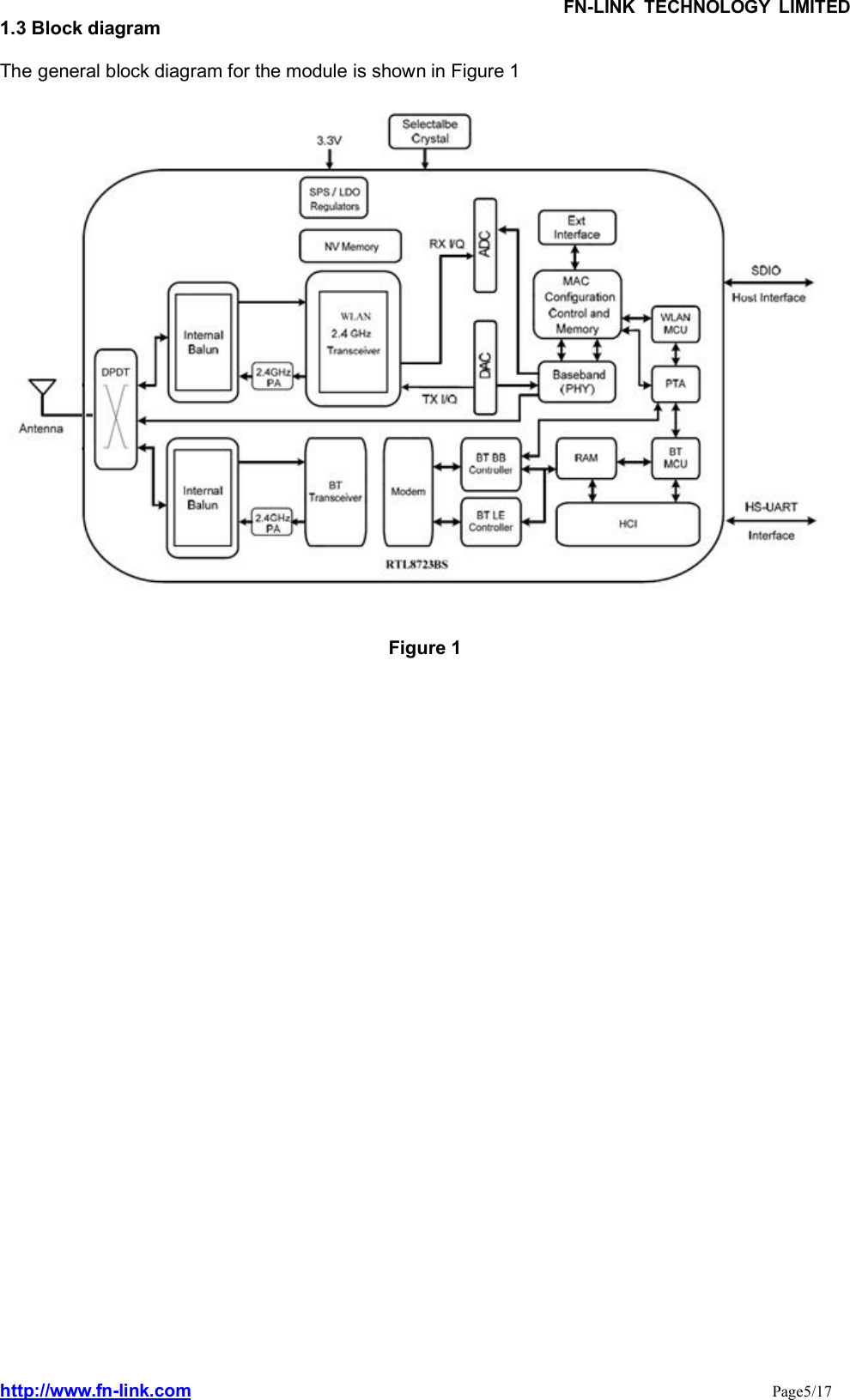
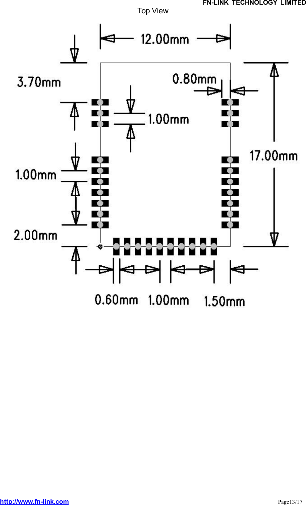
 F23BDSM43 WiFi+BT Module User Manual

FN-LINK TECHNOLOGY LIMITED WiFi+BT Module Users Manual

15_F23BDSM43 UserMan,r1.pdf

Product SpecificationIEEE 802.11 b/g/n 2.4GHz 1T1R WiFi with Bluetooth v2.1+EDR/Bluetooth 3.0/4.0(Single Antenna)Project Name WiFi+BT Module Model NO F23BDSM43Approved: William Tan Checked: Jim Hu Drafted: Neal YuFN-LINK TECHNOLOGY LIMITED5th Floor, A Building, Haoye Logistics Park,Shugang Channel, Bao'an District,Shenzhen City, CHINATEL: 86-0755-29558186FAX: 86-0755-29558196Website: www.fn-link.com
FN-LINK TECHNOLOGY LIMITEDhttp://www.fn-link.com Page2/17CONTENTS0 REVESION HISTORY.................................................................................................................................... 31 INTRODUCTIONS.......................................................................................................................................... 41.1 OVERVEIW.............................................................................................................................................. 41.2 PRODUCT FEATURES..........................................................................................................................41.3 BLOCK DIAGRAM.................................................................................................................................. 52 GENERAL SPECIFICATION......................................................................................................................... 63 ELECTRICAL CHARACTERISTICS............................................................................................................ 83.1 POWER SUPPLY DC CHARACTERISTICS......................................................................................83.2 DIGITAL I/O PIN DC CHARACTERISTICS........................................................................................ 83.3 SDIO INTERFACE AC CHARACTERISTICS.................................................................................... 83.4 SDIO INTERFACE POWER-ON SEQUENCE.................................................................................. 93.5 UART INTERFACE POWER-ON SEQUENCE............................................................................... 104 PIN DEFINITION........................................................................................................................................... 115 MECHANICAL SPECIFICATION............................................................................................................... 145.1 OUTLINE DRAWING........................................................................................................................... 145.2 RECOMMENDED REFLOW PROFILE............................................................................................ 155.3 NOTICE.................................................................................................................................................. 156 PACKAGE...................................................................................................................................................... 16
FN-LINK TECHNOLOGY LIMITEDhttp://www.fn-link.com Page3/170. Revision HistoryREV NO Date Modifications Draft ApprovedNeal YuFirst Released2016-03-05REV 1.0 William Tan
FN-LINK TECHNOLOGY LIMITEDhttp://www.fn-link.com Page4/171. Introduction1.1 OverviewF23BDSM43 is a small size and low profile WiFi   +    BT Combo module, The size is 12mm*17mm.  Itcan be easily manufactured on SMT process and highly suitable for tablet PC, ultra book, mobiledevice and consumer products. It provides SDIO interface for WiFi to connect with host processor andhigh speed UART interface for BT. It also has a PCM interface for audio data transmission with directlink to external audio codec via BT controller. The WiFi throughput can go up to 150Mbps in theory byusing 1x1 802.11 b/g/n MIMO technology and Bluetooth can support BT2.1+EDR/BT3.0 and BT4.0.F23BDSM43 uses  Realtek  RTL8723BS.  It is a highly integrated 802.11b/g/n  1T1R WLAN, anintegrated Bluetooth 2.1/3.0/4.0 module. It combines a WLAN MAC, a 1T1R capable WLAN baseband,BT protocol Stack(LM, LL, and LE), BT baseband, modem, and WLAN/BT RF in the module. TheNF23BDSM43provides  a complete  solution  for a high throughput performance integrated wirelessLAN and Bluetooth controller.1.2 Product FeaturesGeneral12mm*17mm802.11b/g/n 1T1R WLAN and Bluetooth moduleHost InterfaceComplies with SDIO 1.1/2.0/3.0 for WLAN with clock rate up to 100MHz (DDR50)Complies with HS-UART with configurable baud rate for BluetoothWLAN FeaturesCMOS MAC, Baseband PHY, and RF in a single chip for 802.11b/g/n compatible WLANComplete 802.11n solution for 2.4GHz bandOne Transmit and one Receive path (1T1R)Short Guard Interval (400ns)Maximum data rate 54Mbps in 802.11g; and 150Mbps in 802.11n802.11i (WPA, WPA2). Open, shared key, and pair-wise key authentication servicesBT FeaturesCompatible with Bluetooth v2.1+EDR and v3.0 SystemsSupports Bluetooth 4.0 Low Energy(BLE)Integrated MCU to execute Bluetooth protocol stackPCM interface for audio data transmission via Bluetooth controllerSupports AFH to dynamically detect channel quality to improve transmission quality
FN-LINK TECHNOLOGY LIMITEDhttp://www.fn-link.com Page5/171.3 Block diagramThe general block diagram for the module is shown in Figure 1Figure 1
FN-LINK TECHNOLOGY LIMITEDhttp://www.fn-link.com Page6/172. General specificationGeneral featuresMain Chipset Realtek RTL8723BSHost Interface SDIO for WLANUART for BTWiFi Standards 802.11b/g/nBT Standards Bluetooth 2.1/3.0/4.0Dimension L17.0mm*W12.0mm*H1.7mmOperating conditionsOperating Voltage 3.3±10% VdcOperating Temperature 0°C to +70°CStorage Temperature -40°C to +80°CRF featuresOperating Frequency 2.400~2.4835GHzChannelsWiFi:USA/Canada: channel 1~11;BT:Channel 0~78ModulationWiFi:802.11b(DSSS): CCK(11, 5.5Mbps), DQPSK(2Mbps), DBPSK(1Mbps);802.11g(OFDM): BPSK(9,6Mbps), QPSK(18,12Mbps),16QAM(36,24Mbps), 64QAM(54,48Mbps);802.11n(OFDM): BPSK, QPSK, 16QAM, 64QAM(150Mbps)BT:8DPSK, π /4 DQPSK, GFSKPHY Data ratesWiFi:802.11b: 11,5.5,2,1 Mbps802.11g: 54,48,36,24,18,12,9,6 Mbps802.11n: up to 150MbpsBT:1 Mbps for Basic Rate2,3 Mbps for Enhanced Data RateOutput PowerWiFi:802.11b <16dBm802.11g <15dBm802.11n <14dBmBT:Max <10dBm
FN-LINK TECHNOLOGY LIMITEDhttp://www.fn-link.com Page7/17EVM802.11b EVM≦35%802.11g EVM≦-25dB802.11n EVM≦-28dBSensitivityWiFi:802.11b@8% PER1Mbps -88dBm2Mbps -87dBm5.5Mbps -85dBm11Mbps -82dBm802.11g@10% PER6Mbps -86dBm9Mbps -85dBm12Mbps -84dBm18Mbps -82dBm24Mbps -80dBm36Mbps -77dBm48Mbps -73dBm54Mbps -71dBm802.11n_HT20@10% PERMCS 0 -83dBmMCS 1 -82dBmMCS 2 -80dBmMCS 3 -78dBmMCS 4 -75dBmMCS 5 -71dBmMCS 6 -69dBmMCS 7 -67dBmBT:-89dBm @ 1Mbps-86dBm @ 2Mbps-83dBm @ 3MbpsOther featuresAntenna Chip Antenna (Single Antenna)Network ArchitectureWiFi:Ad-hoc mode (Peer-to-Peer )Infrastructure modeSoftware APWiFi DirectBT: Pico Net, Scatter NetSecurityWiFi: WPA, WPA-PSK, WPA2, WPA2-PSK, WEP 64bit & 128bit, IEEE802.11x, IEEE 802.11iBT: Simple ParingOS Supported Android /Linux/ Win CE /XP/WIN7/iOS
FN-LINK TECHNOLOGY LIMITEDhttp://www.fn-link.com Page8/173. Electrical Characteristics3.1 Power Supply DC CharacteristicsSymbol Parameter Minimum Typical Maximum UnitVIN33 3.3V Supply Voltage 3.0 3.3 3.6 VVDDIO DC supply for digital I/O 1.62 1.8-3.3 3.6 V3.2 Digital I/O Pin 1.8V DC CharacteristicsSymbol Parameter Minimum Typical Maximum UnitVIH Input high voltage 1.7 1.8 2.0 VVIL Input low voltage - 0 0.8 VVOH Output high voltage 1.62 - 1.8 VVOL Output low voltage 0 - 0.18 V3.3 Digital I/O Pin 3.3V DC CharacteristicsSymbol Parameter Minimum Typical Maximum UnitVIH Input high voltage 2.0 3.3 3.6 VVIL Input low voltage - 0 0.9 VVOH Output high voltage 2.97 - 3.3 VVOL Output low voltage 0 - 0.33 V3.4 SDIO/GSPI Interface AC CharacteristicsFigure 2. SDIO Interface TimingSDIO Interface Timing ParametersNO Parameter Mode MIN MAX UnitfPP Clock Frequency Default 0 25 MHzHS 0 50 MHzTWL Clock Low Time DEF 10 - nsHS 7 - nsTWH Clock High Time DEF 10 - nsHS 7 - nsTISU Input Setup Time DEF 5 - nsHS 6 - nsTIH Input Hold Time DEF 5 - nsHS 2 - nsTODLY Output Delay Time DEF - 14 nsHS - 14 ns
FN-LINK TECHNOLOGY LIMITEDhttp://www.fn-link.com Page9/173.4 SDIO Interface Power-On SequenceAfter power-on, the SDIO interface is selected by the RTL8723BS automatically when a valid SDIOcommand is received. To attain better SDIO host compatibility, the following power-on sequence isRecommended.Figure 3. SDIO Interface Power-On SequenceSDIO Interface Power-On SequenceSymbol DescriptionT33ramp’3.3V Power Pre-Charge Ramp Up Duration Before Formal Power Up.We recommend that a 3.3V power-on and then power-off sequence isexecuted by the host controller before the formal power on sequence. Thisprocedure can eliminate host card detection issues when power ramp upduration is too long, or when a system warm reboot fails.Toff The duration 3.3V is cut off before formal power up.T33ramp The 3.3V main power ramp up duration.T12ramp The internal 1.2V ramp up duration.TPORThe duration from when the power-on reset releases and the powermanagement unit executes power on tasks. A power on reset will detect both3.3V and 1.2V power ramp up after a predetermined duration.Tnon_rdySDIO Not Ready Duration.In this state, the RTL8723BS-VD may respond to commands without the readybit being set. After theready bit is set, the host will initiate complete card detection procedure.We recommend that the card detection procedures are divided into two phases: A 3.3V powerpre-charge phase and a formal power-up phase.During the 3.3V power pre-charge phase, the power ramp up duration is not limited. The 3.3V power iscut off and is turned on after the Toff period. The ramp up time is specified in the T33ramp duration.After main 3.3V ramp up and 1.2V ramp up, the power management unit is enabled by the power readydetection circuit. The power management unit enables the SDIO block. eFUSE is then autoloaded toSDIO circuits during the Tnon_rdy duration. After the autoload has completed, the SDIO sets the readybit. After CMD5/5/3/7 procedures, card detection is executed. When the driver has loaded, normalCMD52 and CMD53 are used.
FN-LINK TECHNOLOGY LIMITEDhttp://www.fn-link.com Page10/17SDIO Interface Power-On Timing ParametersSymbol MIN Typical MAX UnitT33ramp’ - - No Limit msToff 250 500 1000 msT33ramp 0.1 0.5 2.5 msT12ramp 0.1 0.5 1.5 msTPOR 2 2 8 msTnon_rdy 1 2 10 ms3.5 UART Interface Power-On SequenceFigure 4. UART Power On Sequence With Hardware Flow ControlUART Interface Power-On SequenceSymbol DescriptionT33ramp’3.3V Power Pre-Charge Ramp Up Duration Before Formal Power Up.We recommend that a 3.3V power-on and then power-off sequence isexecuted by the host controller before the formal power on sequence. Thisprocedure can eliminate host card detection issues whenpower ramp up duration is too long, or when a system warm reboot fails.Toff The duration 3.3V is cut off before formal power up.T33ramp The 3.3V main power ramp up duration.T12ramp The internal 1.2V ramp up duration.TPORThe duration from when the power-on reset releases and the powermanagement unit executes power on tasks. A power on reset will detect both3.3V and 1.2V power ramp up after a predetermined duration.Tnon_rdy UART Not Ready Duration.In this state, the RTL8723BS-VD will not respond to any commands.We recommend that the card detection procedures are divided into two phases: A 3.3V powerpre-charge phase and a formal power-up phase.During the 3.3V power pre-charge phase, the power ramp up duration is not limited. The 3.3V power iscut off and is turned on after the Toff period. The ramp up time is specified in the T33ramp duration.After main 3.3V ramp up and 1.2V ramp up, the power management unit is enabled by the power readydetection circuit. The power management unit enables the Bluetooth block. The Bluetooth firmware
FN-LINK TECHNOLOGY LIMITEDhttp://www.fn-link.com Page11/17theninitializes all circuits, included the UART. In addition to wait the Tnon_rdy time, if the host supportsUART hardware flow control it can detect RTS signals and follow the formal UART flow controlhandshake.UART Interface Power On Timing ParametersSymbol MIN Typical MAX UnitT33ramp’ - - No Limit msToff 250 500 1000 msT33ramp 0.1 0.5 2.5 msT12ramp 0.1 0.5 1.5 msTPOR 2 2 8 msTnon_rdy 1 2 10 ms4. Pin Definition(Top View)Pin AssignmentPin# Name Description Remark1 GND Ground2 ANT1 Antenna 13 GND Ground4 PCM_IN PCM data Input High level: 1.8V5 PCM_OUT PCM data Output High level: 1.8V6 PCM_CLK PCM Clock7 PCM_SYNC PCM Synchronization control8 GND Ground9 BT_WAKE_HOST_DEV10 HST_WAKE_BT Host wake up BT, active high
FN-LINK TECHNOLOGY LIMITEDhttp://www.fn-link.com Page12/1711 UART_CTS High-Speed UART CTS12 UART_IN High-Speed UART Data In VDDIO13 UART_OUT High-Speed UART Data Out VDDIO14 GND Ground VDDIO15 SD_CLK SDIO Clock Input VDDIO16 SD_CMD SDIO Command Line VDDIO17 SD_D0 SDIO Data Line 0 VDDIO18 SD_D1 SDIO Data Line 1 VDDIO19 SD_D2 SDIO Data Line 2 VDDIO20 SD_D3 SDIO Data Line 3 VDDIO21 GND Ground22 3.3V 3.3V Power Supply VDDIO23 VDDIO Digital IO Supply Voltage24 SUSCLK_IN External sleep clock input(32.768kHz)25 WLAN_WAKE_HOST VDDIO26 WL_ENABLE Wlan Radio-off Function VDDIO27 BT_RESET BT Radio-off Function VDDIO28 GND Ground29 ANT2 Antenna 230 GND ground5.Mechanical Specification5.1 Outline Drawing(Unit: mm)(Top Side) (Bottom Side)
FN-LINK TECHNOLOGY LIMITEDhttp://www.fn-link.com Page13/17Top View
FN-LINK TECHNOLOGY LIMITEDhttp://www.fn-link.com Page14/175.2 Recommended Reflow ProfileReferred to IPC/JEDEC standard.Peak Temperature : <250°CNumber of Times : ≤2 times5.3 Patch WIFI modules installed before the notice:WIFI module installed note:1. Please press 1 : 1 and then expand outward proportion to 0.7 mm, 0.12 mm thickness When open astencil2. Take and use the WIFI module, please insure the electrostatic protective measures.3. Reflow soldering temperature should be according to the customer the main size of the products,such as the temperature set at 250 + 5 ℃for the MID motherboard.About the module packaging, storage and use of matters needing attention are as follows:1. The module of the reel and storage life of vacuum packing: 1). Shelf life: 8 months, storageenvironment conditions: temperature in: < 40 ℃, relative humidity: < 90% r.h.2. The module vacuum packing once opened, time limit of the assembly:Card: 1) check the humidity display value should be less than 30% (in blue), such as: 30% ~ 40%(pink), or greater than 40% (red) the module have been moisture absorption.2.) factory environmental temperature humidity control: ≦30 ℃,≦60% r.h..3). Once opened, the workshop the preservation of life for 168 hours.3. Once opened, such as when not used up within 168 hours:1). The module must be again to remove the module moisture absorption.2). The baking temperature: 125 ℃, 8 hours.3.) After baking, put the right amount of desiccant to seal packages.
FN-LINK TECHNOLOGY LIMITEDhttp://www.fn-link.com Page15/176. Package6.1 Reel Packaging2000pcs/reel
FCC Statement: This device complies with Part 15 of the FCC Rules. Operation is subject to the following two conditions: (1) This device may not cause harmful interference. (2) This device must accept any interference received, including interference that may cause undesired operation.    NOTE: This equipment has been tested and found to comply with the limits for a Class B digital device, pursuant to Part 15 of the FCC Rules. These limits are designed to provide reasonable protection against harmful interference in a residential installation. This equipment generates uses and can radiate radio frequency energy and, if not installed and used in accordance with the instructions, may cause harmful interference to radio communications. However, there is no guarantee that interference will not occur in a particular installation. If this equipment does cause harmful interference to radio or television reception, which can be determined by turning the equipment off and on, the user is encouraged to try to correct the interference by one or more of the following measures:   ---Reorient or relocate the receiving antenna. ---Increase the separation between the equipment and receiver.     ---Connect the equipment into an outlet on a circuit different from that to which the receiver is connected. ---Consult the dealer or an experienced radio/TV technician for help.  WARNING: Changes or modifications not expressly approved by the party responsible for compliance could void the user's authority to operate the equipment.    LABEL OF THE END PRODUCT: The final end product must be labelled in a visible area with the following "Contains TX FCC ID: 2AATL-F23BDSM43". If the size of the end product is smaller than 8x10cm, then additional FCC part 15.19 statement is required to be available in the users manual: This device complies with Part 15 of the FCC Rules. Operation is subject to the following two conditions: (1) this device may not cause harmful interference, and (2) this device must accept any interference received, including interference that may cause undesired operation.  RF Exposure This device has been evaluated and shown compliant with the FCC RF Exposure limits under fixed exposure conditions (antennas are greater than 20cm from a person's body) when installed in certain specific OEM configurations. This modular complies with FCC RF radiation exposure limits set forth for an uncontrolled environment. This transmitter must not be co-located or operating in conjunction with any other antenna or transmitter. Due to missing shielding the module is strictly limited to integration by the Grantee himself or his dedicated    OEM integrator under control of the Grantee. However, the OEM integrator is still responsible for testing their end-product for any additional compliance requirements required with this module installed.    FN-LINK TECHNOLOGY LIMITEDhttp://www.fn-link.com Page16/17
IMPORTANT NOTE:   This device is intended only for OEM integrators under the following conditions: (1) According to FCC Part 15 Subpart C Section 15.212, the radio elements of the modular transmitter must have their own shielding. However, due to there is no shielding for this WIFI/BT module, this module is granted as a Limited Modular Approval. (2) This module has been designed to operate with a Integral Chip antenna having a maximum gain of 1.5dBi. Only this type of antenna may be used. (3) Integration is typically strictly restricted to Grantee himself or dedicated OEM integrators under control of the Grantee.  In the event that these conditions can not be met (for example certain laptop configurations or co-location with another transmitter. then the FCC authorization is no longer considered valid and the FCC ID can not be used on the final product. In these circumstances, the OEM integrator will be responsible for re-evaluating the end product (including the transmitter) and obtaining a separate FCC authorization. The module will be responsible to satisfy SAR/RF Exposure requirements, when the module integrated into any (portable, mobile, fixed) host device. This module is intended for OEM integrator only and the OEM integrators and instructed to ensure that the end user has no manual instructions to remove or install the device. The OEM integrator is still responsible for the FCC compliance requirement of the end product, which integrates this module.  The module has no shielding and tested stand alone. This module is tested and approved as Limited modular approval with stand alone configuration, any OEM incorporated this radio module into any system are require additional testing and evaluation. The module is only certified with the installed antenna. Any change of the antenna will void the certification. The host device including this RF module need to undergo separate certification.           FN-LINK TECHNOLOGY LIMITEDhttp://www.fn-link.com Page17/17The OEM integrator has to be aware not to provide information to the end use regarding how to install or remove this RF module in the user's manual of the end product which integrates this module. The end user manual shall include all required regulatory information/warming as shown in this manual.

Navigation menu