HUNAN FN LINK TECHNOLOGY F23BDSM43 WiFi+BT Module User Manual
FN-LINK TECHNOLOGY LIMITED WiFi+BT Module Users Manual
15_F23BDSM43 UserMan,r1.pdf

Product Specification
IEEE 802.11 b/g/n 2.4GHz 1T1R WiFi with Bluetooth v2.1+EDR/Bluetooth 3.0/4.0
(Single Antenna)
Project Name WiFi+BT Module
Model NO F23BDSM43
Approved: William Tan Checked: Jim Hu Drafted: Neal Yu
FN-LINK TECHNOLOGY LIMITED
5th Floor, A Building, Haoye Logistics Park,
Shugang Channel, Bao'an District,
Shenzhen City, CHINA
TEL: 86-0755-29558186
FAX: 86-0755-29558196
Website: www.fn-link.com

FN-LINK TECHNOLOGY LIMITED
http://www.fn-link.com Page2/17
CONTENTS
0 REVESION HISTORY.................................................................................................................................... 3
1 INTRODUCTIONS.......................................................................................................................................... 4
1.1 OVERVEIW.............................................................................................................................................. 4
1.2 PRODUCT FEATURES..........................................................................................................................4
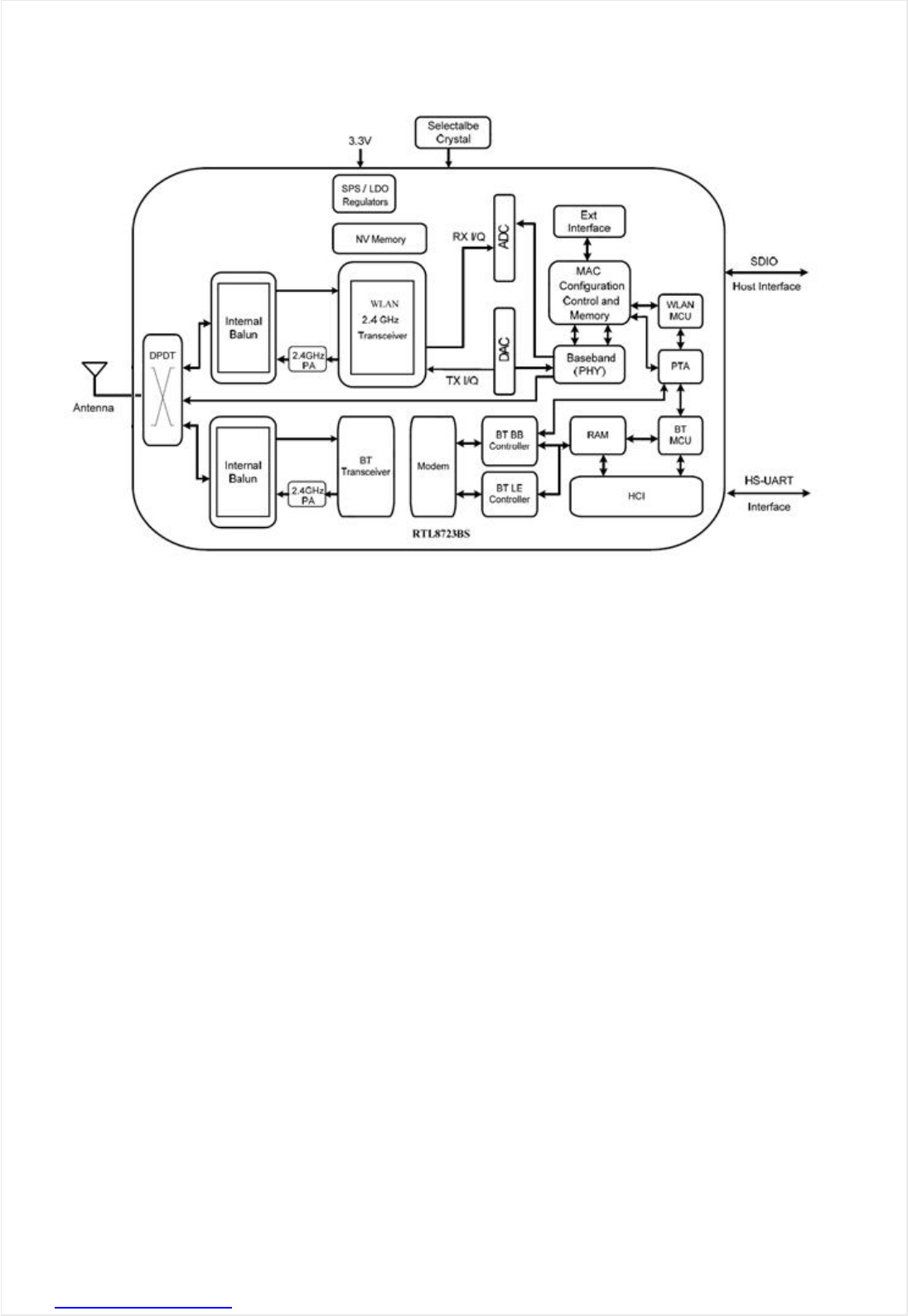
1.3 BLOCK DIAGRAM.................................................................................................................................. 5
2 GENERAL SPECIFICATION......................................................................................................................... 6
3 ELECTRICAL CHARACTERISTICS............................................................................................................ 8
3.1 POWER SUPPLY DC CHARACTERISTICS......................................................................................8
3.2 DIGITAL I/O PIN DC CHARACTERISTICS........................................................................................ 8
3.3 SDIO INTERFACE AC CHARACTERISTICS.................................................................................... 8
3.4 SDIO INTERFACE POWER-ON SEQUENCE.................................................................................. 9
3.5 UART INTERFACE POWER-ON SEQUENCE............................................................................... 10
4 PIN DEFINITION........................................................................................................................................... 11
5 MECHANICAL SPECIFICATION............................................................................................................... 14
5.1 OUTLINE DRAWING........................................................................................................................... 14
5.2 RECOMMENDED REFLOW PROFILE............................................................................................ 15
5.3 NOTICE.................................................................................................................................................. 15
6 PACKAGE...................................................................................................................................................... 16


FN-LINK TECHNOLOGY LIMITED
http://www.fn-link.com Page4/17
1. Introduction
1.1 Overview
F23BDSM43 is a small size and low profile WiFi + BT Combo module, The size is 12mm*17mm. It
can be easily manufactured on SMT process and highly suitable for tablet PC, ultra book, mobile
device and consumer products. It provides SDIO interface for WiFi to connect with host processor and
high speed UART interface for BT. It also has a PCM interface for audio data transmission with direct
link to external audio codec via BT controller. The WiFi throughput can go up to 150Mbps in theory by
using 1x1 802.11 b/g/n MIMO technology and Bluetooth can support BT2.1+EDR/BT3.0 and BT4.0.
F23BDSM43 uses Realtek RTL8723BS. It is a highly integrated 802.11b/g/n 1T1R WLAN, an
integrated Bluetooth 2.1/3.0/4.0 module. It combines a WLAN MAC, a 1T1R capable WLAN baseband,
BT protocol Stack(LM, LL, and LE), BT baseband, modem, and WLAN/BT RF in the module. The
NF23BDSM43provides a complete solution for a high throughput performance integrated wireless
LAN and Bluetooth controller.
1.2 Product Features
General
12mm*17mm
802.11b/g/n 1T1R WLAN and Bluetooth module
Host Interface
Complies with SDIO 1.1/2.0/3.0 for WLAN with clock rate up to 100MHz (DDR50)
Complies with HS-UART with configurable baud rate for Bluetooth
WLAN Features
CMOS MAC, Baseband PHY, and RF in a single chip for 802.11b/g/n compatible WLAN
Complete 802.11n solution for 2.4GHz band
One Transmit and one Receive path (1T1R)
Short Guard Interval (400ns)
Maximum data rate 54Mbps in 802.11g; and 150Mbps in 802.11n
802.11i (WPA, WPA2). Open, shared key, and pair-wise key authentication services
BT Features
Compatible with Bluetooth v2.1+EDR and v3.0 Systems
Supports Bluetooth 4.0 Low Energy(BLE)
Integrated MCU to execute Bluetooth protocol stack
PCM interface for audio data transmission via Bluetooth controller
Supports AFH to dynamically detect channel quality to improve transmission quality

FN-LINK TECHNOLOGY LIMITED
http://www.fn-link.com Page6/17
2. General specification
General features
Main Chipset Realtek RTL8723BS
Host Interface SDIO for WLAN
UART for BT
WiFi Standards 802.11b/g/n
BT Standards Bluetooth 2.1/3.0/4.0
Dimension L17.0mm*W12.0mm*H1.7mm
Operating conditions
Operating Voltage 3.3±10% Vdc
Operating Temperature 0°C to +70°C
Storage Temperature -40°C to +80°C
RF features
Operating Frequency 2.400~2.4835GHz
Channels
WiFi:
USA/Canada: channel 1~11;
BT:
Channel 0~78
Modulation
WiFi:
802.11b(DSSS): CCK(11, 5.5Mbps), DQPSK(2Mbps), DBPSK(1Mbps);
802.11g(OFDM): BPSK(9,6Mbps), QPSK(18,12Mbps),
16QAM(36,24Mbps), 64QAM(54,48Mbps);
802.11n(OFDM): BPSK, QPSK, 16QAM, 64QAM(150Mbps)
BT:
8DPSK, π /4 DQPSK, GFSK
PHY Data rates
WiFi:
802.11b: 11,5.5,2,1 Mbps
802.11g: 54,48,36,24,18,12,9,6 Mbps
802.11n: up to 150Mbps
BT:
1 Mbps for Basic Rate
2,3 Mbps for Enhanced Data Rate
Output Power
WiFi:
802.11b <16dBm
802.11g <15dBm
802.11n <14dBm
BT:
Max <10dBm

FN-LINK TECHNOLOGY LIMITED
http://www.fn-link.com Page7/17
EVM
802.11b EVM≦35%
802.11g EVM≦-25dB
802.11n EVM≦-28dB
Sensitivity
WiFi:
802.11b@8% PER
1Mbps -88dBm
2Mbps -87dBm
5.5Mbps -85dBm
11Mbps -82dBm
802.11g@10% PER
6Mbps -86dBm
9Mbps -85dBm
12Mbps -84dBm
18Mbps -82dBm
24Mbps -80dBm
36Mbps -77dBm
48Mbps -73dBm
54Mbps -71dBm
802.11n_HT20@10% PER
MCS 0 -83dBm
MCS 1 -82dBm
MCS 2 -80dBm
MCS 3 -78dBm
MCS 4 -75dBm
MCS 5 -71dBm
MCS 6 -69dBm
MCS 7 -67dBm
BT:
-89dBm @ 1Mbps
-86dBm @ 2Mbps
-83dBm @ 3Mbps
Other features
Antenna Chip Antenna (Single Antenna)
Network Architecture
WiFi:
Ad-hoc mode (Peer-to-Peer )
Infrastructure mode
Software AP
WiFi Direct
BT: Pico Net, Scatter Net
Security
WiFi: WPA, WPA-PSK, WPA2, WPA2-PSK, WEP 64bit & 128bit, IEEE
802.11x, IEEE 802.11i
BT: Simple Paring
OS Supported Android /Linux/ Win CE /XP/WIN7/iOS
FN-LINK TECHNOLOGY LIMITED
http://www.fn-link.com Page8/17
3. Electrical Characteristics
3.1 Power Supply DC Characteristics
Symbol Parameter Minimum Typical Maximum Unit
VIN33 3.3V Supply Voltage 3.0 3.3 3.6 V
VDDIO DC supply for digital I/O 1.62 1.8-3.3 3.6 V
3.2 Digital I/O Pin 1.8V DC Characteristics
Symbol Parameter Minimum Typical Maximum Unit
VIH Input high voltage 1.7 1.8 2.0 V
VIL Input low voltage - 0 0.8 V
VOH Output high voltage 1.62 - 1.8 V
VOL Output low voltage 0 - 0.18 V
3.3 Digital I/O Pin 3.3V DC Characteristics
Symbol Parameter Minimum Typical Maximum Unit
VIH Input high voltage 2.0 3.3 3.6 V
VIL Input low voltage - 0 0.9 V
VOH Output high voltage 2.97 - 3.3 V
VOL Output low voltage 0 - 0.33 V
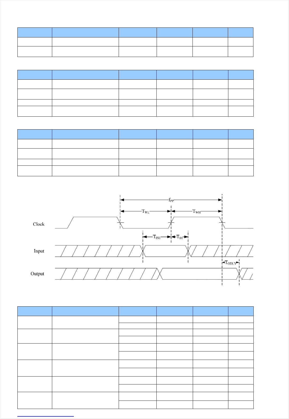
3.4 SDIO/GSPI Interface AC Characteristics
Figure 2. SDIO Interface Timing
SDIO Interface Timing Parameters
NO Parameter Mode MIN MAX Unit
fPP Clock Frequency Default 0 25 MHz
HS 0 50 MHz
TWL Clock Low Time DEF 10 - ns
HS 7 - ns
TWH Clock High Time DEF 10 - ns
HS 7 - ns
TISU Input Setup Time DEF 5 - ns
HS 6 - ns
TIH Input Hold Time DEF 5 - ns
HS 2 - ns
TODLY Output Delay Time DEF - 14 ns
HS - 14 ns
FN-LINK TECHNOLOGY LIMITED
http://www.fn-link.com Page9/17
3.4 SDIO Interface Power-On Sequence
After power-on, the SDIO interface is selected by the RTL8723BS automatically when a valid SDIO
command is received. To attain better SDIO host compatibility, the following power-on sequence is
Recommended.
Figure 3. SDIO Interface Power-On Sequence
SDIO Interface Power-On Sequence
Symbol Description
T33ramp’
3.3V Power Pre-Charge Ramp Up Duration Before Formal Power Up.
We recommend that a 3.3V power-on and then power-off sequence is
executed by the host controller before the formal power on sequence. This
procedure can eliminate host card detection issues when power ramp up
duration is too long, or when a system warm reboot fails.
Toff The duration 3.3V is cut off before formal power up.
T33ramp The 3.3V main power ramp up duration.
T12ramp The internal 1.2V ramp up duration.
TPOR
The duration from when the power-on reset releases and the power
management unit executes power on tasks. A power on reset will detect both
3.3V and 1.2V power ramp up after a predetermined duration.
Tnon_rdy
SDIO Not Ready Duration.
In this state, the RTL8723BS-VD may respond to commands without the ready
bit being set. After the
ready bit is set, the host will initiate complete card detection procedure.
We recommend that the card detection procedures are divided into two phases: A 3.3V power
pre-charge phase and a formal power-up phase.
During the 3.3V power pre-charge phase, the power ramp up duration is not limited. The 3.3V power is
cut off and is turned on after the Toff period. The ramp up time is specified in the T33ramp duration.
After main 3.3V ramp up and 1.2V ramp up, the power management unit is enabled by the power ready
detection circuit. The power management unit enables the SDIO block. eFUSE is then autoloaded to
SDIO circuits during the Tnon_rdy duration. After the autoload has completed, the SDIO sets the ready
bit. After CMD5/5/3/7 procedures, card detection is executed. When the driver has loaded, normal
CMD52 and CMD53 are used.
FN-LINK TECHNOLOGY LIMITED
http://www.fn-link.com Page10/17
SDIO Interface Power-On Timing Parameters
Symbol MIN Typical MAX Unit
T33ramp’ - - No Limit ms
Toff 250 500 1000 ms
T33ramp 0.1 0.5 2.5 ms
T12ramp 0.1 0.5 1.5 ms
TPOR 2 2 8 ms
Tnon_rdy 1 2 10 ms
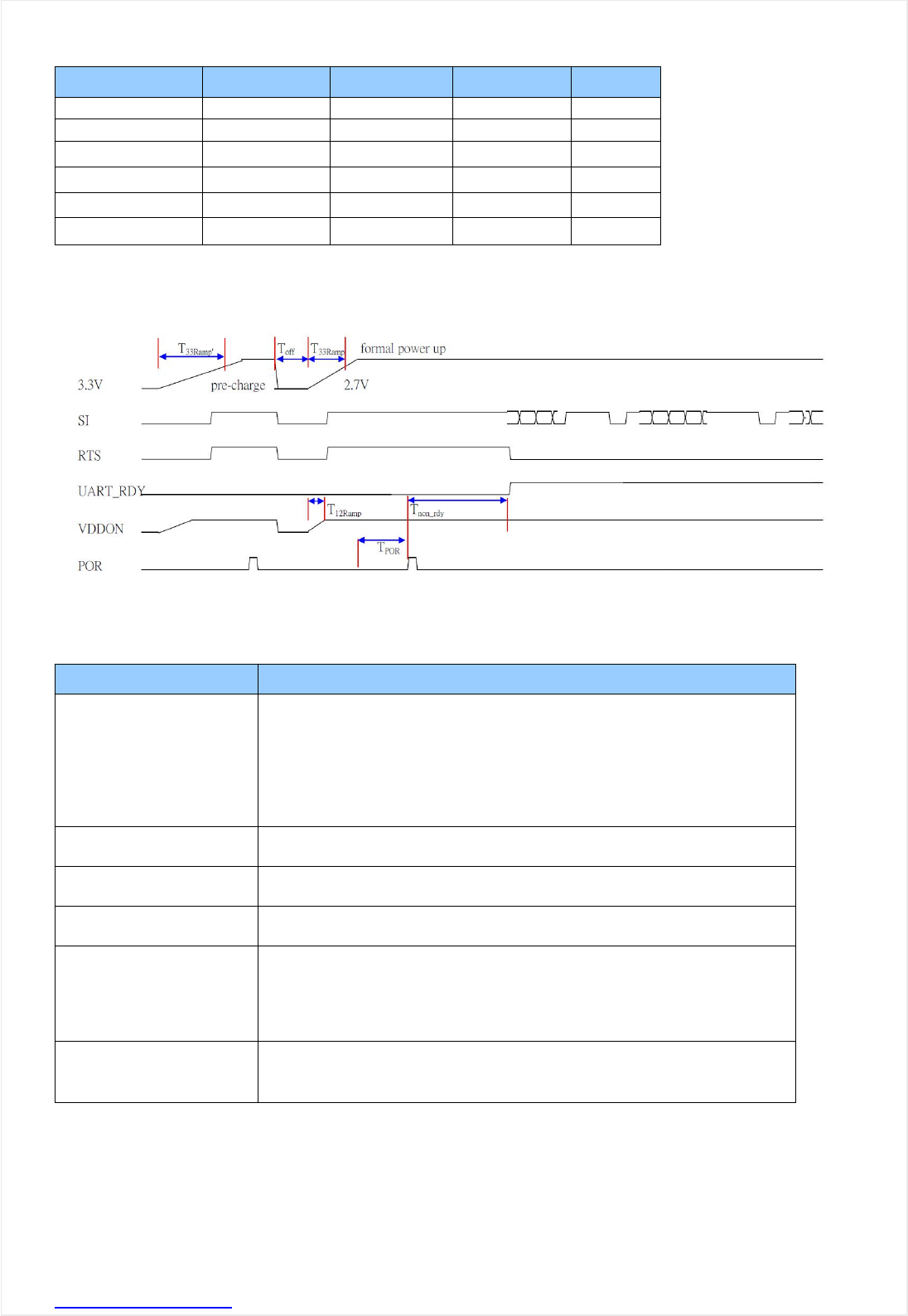
3.5 UART Interface Power-On Sequence
Figure 4. UART Power On Sequence With Hardware Flow Control
UART Interface Power-On Sequence
Symbol Description
T33ramp’
3.3V Power Pre-Charge Ramp Up Duration Before Formal Power Up.
We recommend that a 3.3V power-on and then power-off sequence is
executed by the host controller before the formal power on sequence. This
procedure can eliminate host card detection issues when
power ramp up duration is too long, or when a system warm reboot fails.
Toff The duration 3.3V is cut off before formal power up.
T33ramp The 3.3V main power ramp up duration.
T12ramp The internal 1.2V ramp up duration.
TPOR
The duration from when the power-on reset releases and the power
management unit executes power on tasks. A power on reset will detect both
3.3V and 1.2V power ramp up after a predetermined duration.
Tnon_rdy UART Not Ready Duration.
In this state, the RTL8723BS-VD will not respond to any commands.
We recommend that the card detection procedures are divided into two phases: A 3.3V power
pre-charge phase and a formal power-up phase.
During the 3.3V power pre-charge phase, the power ramp up duration is not limited. The 3.3V power is
cut off and is turned on after the Toff period. The ramp up time is specified in the T33ramp duration.
After main 3.3V ramp up and 1.2V ramp up, the power management unit is enabled by the power ready
detection circuit. The power management unit enables the Bluetooth block. The Bluetooth firmware
FN-LINK TECHNOLOGY LIMITED
http://www.fn-link.com Page11/17
theninitializes all circuits, included the UART. In addition to wait the Tnon_rdy time, if the host supports
UART hardware flow control it can detect RTS signals and follow the formal UART flow control
handshake.
UART Interface Power On Timing Parameters
Symbol MIN Typical MAX Unit
T33ramp’ - - No Limit ms
Toff 250 500 1000 ms
T33ramp 0.1 0.5 2.5 ms
T12ramp 0.1 0.5 1.5 ms
TPOR 2 2 8 ms
Tnon_rdy 1 2 10 ms
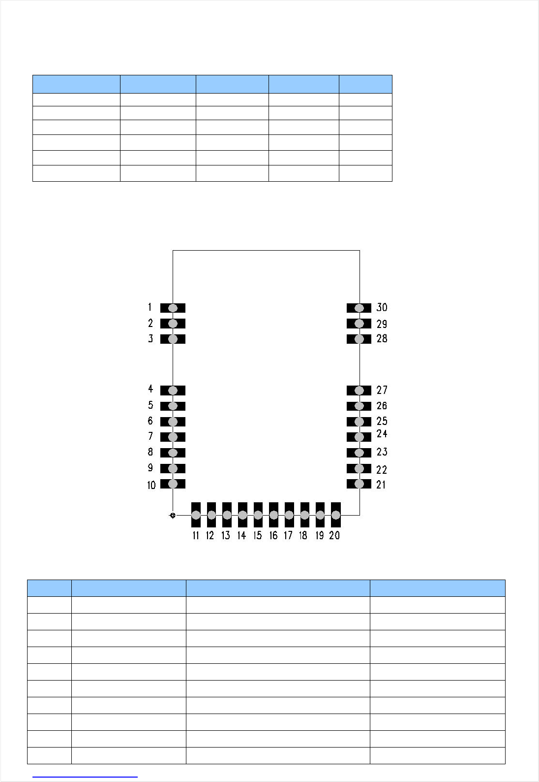
4. Pin Definition(Top View)
Pin Assignment
Pin# Name Description Remark
1 GND Ground
2 ANT1 Antenna 1
3 GND Ground
4 PCM_IN PCM data Input High level: 1.8V
5 PCM_OUT PCM data Output High level: 1.8V
6 PCM_CLK PCM Clock
7 PCM_SYNC PCM Synchronization control
8 GND Ground
9 BT_WAKE_HOST_DEV
10 HST_WAKE_BT Host wake up BT, active high
FN-LINK TECHNOLOGY LIMITED
http://www.fn-link.com Page12/17
11 UART_CTS High-Speed UART CTS
12 UART_IN High-Speed UART Data In VDDIO
13 UART_OUT High-Speed UART Data Out VDDIO
14 GND Ground VDDIO
15 SD_CLK SDIO Clock Input VDDIO
16 SD_CMD SDIO Command Line VDDIO
17 SD_D0 SDIO Data Line 0 VDDIO
18 SD_D1 SDIO Data Line 1 VDDIO
19 SD_D2 SDIO Data Line 2 VDDIO
20 SD_D3 SDIO Data Line 3 VDDIO
21 GND Ground
22 3.3V 3.3V Power Supply VDDIO
23 VDDIO Digital IO Supply Voltage
24 SUSCLK_IN External sleep clock input(32.768kHz)
25 WLAN_WAKE_HOST VDDIO
26 WL_ENABLE Wlan Radio-off Function VDDIO
27 BT_RESET BT Radio-off Function VDDIO
28 GND Ground
29 ANT2 Antenna 2
30 GND ground
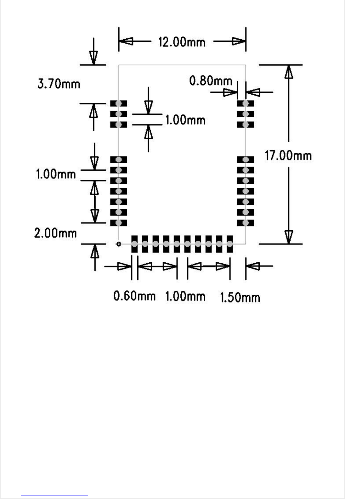
5.Mechanical Specification
5.1 Outline Drawing(Unit: mm)
(Top Side) (Bottom Side)
FN-LINK TECHNOLOGY LIMITED
http://www.fn-link.com Page14/17
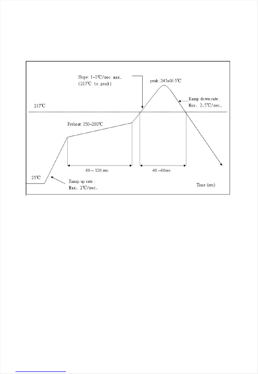
5.2 Recommended Reflow Profile
Referred to IPC/JEDEC standard.
Peak Temperature : <250°C
Number of Times : ≤2 times
5.3 Patch WIFI modules installed before the notice:
WIFI module installed note:
1. Please press 1 : 1 and then expand outward proportion to 0.7 mm, 0.12 mm thickness When open a
stencil
2. Take and use the WIFI module, please insure the electrostatic protective measures.
3. Reflow soldering temperature should be according to the customer the main size of the products,
such as the temperature set at 250 + 5 ℃for the MID motherboard.
About the module packaging, storage and use of matters needing attention are as follows:
1. The module of the reel and storage life of vacuum packing: 1). Shelf life: 8 months, storage
environment conditions: temperature in: < 40 ℃, relative humidity: < 90% r.h.
2. The module vacuum packing once opened, time limit of the assembly:
Card: 1) check the humidity display value should be less than 30% (in blue), such as: 30% ~ 40%
(pink), or greater than 40% (red) the module have been moisture absorption.
2.) factory environmental temperature humidity control: ≦30 ℃,≦60% r.h..
3). Once opened, the workshop the preservation of life for 168 hours.
3. Once opened, such as when not used up within 168 hours:
1). The module must be again to remove the module moisture absorption.
2). The baking temperature: 125 ℃, 8 hours.
3.) After baking, put the right amount of desiccant to seal packages.

FCC Statement:
This device complies with Part 15 of the FCC Rules. Operation is subject to the following two
conditions: (1) This device may not cause harmful interference. (2) This device must accept any
interference received, including interference that may cause undesired operation.
NOTE: This equipment has been tested and found to comply with the limits for a Class B digital
device, pursuant to Part 15 of the FCC Rules. These limits are designed to provide reasonable
protection against harmful interference in a residential installation. This equipment generates
uses and can radiate radio frequency energy and, if not installed and used in accordance with
the instructions, may cause harmful interference to radio communications. However, there is no
guarantee that interference will not occur in a particular installation. If this equipment does
cause harmful interference to radio or television reception, which can be determined by turning
the equipment off and on, the user is encouraged to try to correct the interference by one or
more of the following measures:
---Reorient or relocate the receiving antenna.
---Increase the separation between the equipment and receiver.
---Connect the equipment into an outlet on a circuit different from that to which the receiver is
connected.
---Consult the dealer or an experienced radio/TV technician for help.
WARNING: Changes or modifications not expressly approved by the party responsible for
compliance could void the user's authority to operate the equipment.
LABEL OF THE END PRODUCT:
The final end product must be labelled in a visible area with the following "Contains TX FCC ID:
2AATL-F23BDSM43". If the size of the end product is smaller than 8x10cm, then additional
FCC part 15.19 statement is required to be available in the users manual: This device complies
with Part 15 of the FCC Rules. Operation is subject to the following two conditions: (1) this
device may not cause harmful interference, and (2) this device must accept any interference
received, including interference that may cause undesired operation.
RF Exposure
This device has been evaluated and shown compliant with the FCC RF Exposure limits under
fixed exposure conditions (antennas are greater than 20cm from a person's body) when
installed in certain specific OEM configurations.
This modular complies with FCC RF radiation exposure limits set forth for an uncontrolled
environment. This transmitter must not be co-located or operating in conjunction with any other
antenna or transmitter. Due to missing shielding the module is strictly limited to integration by
the Grantee himself or his dedicated OEM integrator under control of the Grantee. However,
the OEM integrator is still responsible for testing their end-product for any additional compliance
requirements required with this module installed.
FN-LINK TECHNOLOGY LIMITED
http://www.fn-link.com Page16/17

IMPORTANT NOTE:
This device is intended only for OEM integrators under the following conditions:
(1) According to FCC Part 15 Subpart C Section 15.212, the radio elements of the modular
transmitter must have their own shielding. However, due to there is no shielding for this WIFI/BT
module, this module is granted as a Limited Modular Approval.
(2) This module has been designed to operate with a Integral Chip antenna having a maximum
gain of 1.5dBi. Only this type of antenna may be used.
(3) Integration is typically strictly restricted to Grantee himself or dedicated OEM integrators
under control of the Grantee.
In the event that these conditions can not be met (for example certain laptop configurations or
co-location with another transmitter. then the FCC authorization is no longer considered valid
and the FCC ID can not be used on the final product. In these circumstances, the OEM
integrator will be responsible for re-evaluating the end product (including the transmitter) and
obtaining a separate FCC authorization.
The module will be responsible to satisfy SAR/RF Exposure requirements, when the module
integrated into any (portable, mobile, fixed) host device.
This module is intended for OEM integrator only and the OEM integrators and instructed to
ensure that the end user has no manual instructions to remove or install the device. The OEM
integrator is still responsible for the FCC compliance requirement of the end product, which
integrates this module.
The module has no shielding and tested stand alone. This module is tested and approved as
Limited modular approval with stand alone configuration, any OEM incorporated this radio
module into any system are require additional testing and evaluation.
The module is only certified with the installed antenna. Any change of the antenna will void the
certification. The host device including this RF module need to undergo separate certification.
FN-LINK TECHNOLOGY LIMITED
http://www.fn-link.com Page17/17
The OEM integrator has to be aware not to provide information to the end use
regarding how to install or remove this RF module in the user's manual of
the end product which integrates this module. The end user manual shall
include all required regulatory information/warming as shown in this manual.