HYT Science and Technology Co TC3000V Two-Way Radio User Manual
Shenzhen HYT Science &Technology; Co Ltd Two-Way Radio Users Manual
UserManual.wiki
>
HYT Science and Technology Co
>
TC3000V User Manual
>
Users Manual
Contents
1.
Users Manual
2.
Revised user manual
Users Manual
Navigation menu
Upload a User Manual
Namespaces
Wiki Guide
HTML
PDF
Info
Views
User Manual
Discussion / Help
Navigation
![3Brief Introduction (1) Antenna Used to transmit/receive signals. (2) LED Following table indicates LED indication and corresponding radio status. LED Status No display Standby Green Receive Red Transmit Flashing green Scan Flashing red Low battery voltage Flashing orange Call waiting (3) Channel Selector Used to select wanted channel. (4) Programmable key [A] (5) Power/Volume Control Knob Rotate the Power/Volume Knob clockwise until a “click” is heard to turn the radio on, fully counter clockwise to turn the radio off. When the radio is on, turn the knob to adjust volume. (6) Battery Latch Used to fasten the battery. (7) Speaker Used to output sounds. (8) Microphone Used to input sounds. (9) External Jack Used to connect with external earphone or programming cable. (10) Belt Clip Used to clip the radio on your belt.](https://usermanual.wiki/HYT-Science-and-Technology-Co/TC3000V.Users-Manual/User-Guide-486643-Page-3.png)
![4(11) Battery Pack (12) PTT key Press and hold PTT, radio operates in transmit mode. Release PTT, radio returns to receive mode. (13) Programmable Key [B] (14) Programmable Key [C] The following table shows the key function when briefly pressed, pressed and held or held down: Key function Key Function Briefly Press Press and Hold Hold DownEmergency Siren Enable emergency siren Disable emergency siren - Monitor - - Monitor Scan Enable/Disable scan Enable/Disable scan - Nuisance Delete Delete nuisance channel in scan Delete nuisance channel in scan - Select High/Low Power Select High/Low Power Select High/Low Power - Repeater/Talk Around Select Repeater or Talk Around Mode Select Repeater or Talk Around Mode - Repeater/Reverse Frequency Select Repeater or Reverse Frequency ModeSelect Repeater or Reverse Frequency Mode - Call Transmit a Call Transmit a Call - Note: Please contact your dealer for more details about programmable keys.](https://usermanual.wiki/HYT-Science-and-Technology-Co/TC3000V.Users-Manual/User-Guide-486643-Page-4.png)

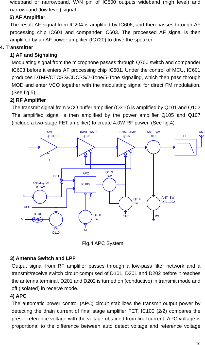
![16Adjustment Description Required Test Instrument Radio communication test set 1 set Scanner 1 set 3A/10V power supply 1 set Digital voltmeter 1 set 3A Ammeter 1 set Preparation Open the programming software in PC and operate as the following instructions. 1. Programme Download: Connect the radio with the computer via programming cable. And then turn the power on. LED glows red. Click “Programme” → “Download” on the interface to choose programme. Click “Open” to begin download and LED flashes red. When download is complete, click “End” and turn the power off. And then disconnect the programming cable. 2. Initialization: Turn the power on while holding down [PTT] and [A] key simultaneously. LED glows orange and a BEEP sounds. Radio channel frequency and setting data are initialized. 3. Destination Set: Connect the radio with the computer via programming cable. And then turn the power on. LED glows red. Set “frequency range” on the programming software interface. And then click “Programme” → “ Writing”. 4. Factory Setting The compander is open. Squelch level 2. Adjustment mode is disabled. Adjustment VCO Measurement Adjustment Item Condition Test Instrument Terminal Part Method Specification/Remarks 1. Setting Power supply 7.5V 1.Turn to CH1. PressPTT. TX High Check 3.3V±0.2V 2.Transmit VCO lock voltage 2. Press PTT again.TX Low Check 1.0V±0.4V 1. Turn to CH2. PressPTT. TX High Check 3.1V±0.2V 3. Receiving VCO lock voltage 2. Press PTT again.TX Low Digital Voltmeter CV TC350 TC351 Check 1.0V±0.4V](https://usermanual.wiki/HYT-Science-and-Technology-Co/TC3000V.Users-Manual/User-Guide-486643-Page-16.png)
![17 Transmitter Measurement Adjustment Item Condition Test Instrument Terminal Part Method Specification/Remarks 1. Transmit frequency Turn to CH3. Press PTT. Radio Communication Test Set ANT [B] (up) [C] (down) Adjust to center frequency. Press [A] to save. Error≤150Hz 1. Turn to CH4. Press PTT. Center frequency Adjust to 4.0 W, I≤1.6A. Press [A] to save. 2. Press PTT.Frequency changes tolow frequency. Adjust to 4.0 W, I≤1.6A. Press [A] to save. High 3. Press PTT again.Frequency changes tohigh frequency. Adjust to 4.0 W, I≤1.6A. Press [A] to save. 4.0W±0.3W 4.0W±0.3W 1. Turn to CH5. Press PTT. Center frequency. Adjust to 1.0 W, I≤0.7A. Press [A] to save. 2. Press PTT.Frequency changes to low frequency. Adjust to 1.0 W, I≤0.7A. Press [A] to save. 2. Power Low 3. Press PTT again.Frequency changes tohigh frequency. Radio Communication Test Set Ammeter ANT [B] (up) [C] (down)Adjust to 1.0 W, I≤0.7A. Press [A] to save. 1W±0.3W 1. Turn to CH6. Press PTT. The radio operateswith wideband. Center frequency. 2. Press PTT.Frequency changes to low frequency. 3. CDCSS balance Wideba-nd Narrow-band 3. Press PTT again.Frequency changes tohigh frequency. Radio Communication Test Set LPF: 15KHz ANT [B] (up) [C] (down) Rectify the waveform to square wave. Press [A] to save.](https://usermanual.wiki/HYT-Science-and-Technology-Co/TC3000V.Users-Manual/User-Guide-486643-Page-17.png)
![18 4. Press [A] for twoseconds. LED flashesindicating that theradio operates withnarrowband. Center frequency. Adjust narrowbandfollowing the abovesteps. Wideba-nd 1. Turn to CH7. Press PTT. The radio operateswith wideband. Center frequency. Adjust it to 4.0KHz±100Hz. Press [A] to save. 4. Maximu-m frequenc-y deviation Narrow-band 2. Press [A] for twoseconds. LED flashesindicating that theradio operates with narrowband. Center frequency. Radio Communication Test Set LPF: 15KHz AF: 1KHz 1V ANT MIC Jack [B] (up) [C] (down) Adjust it to 2.0KHz±100Hz. Press [A] to save. 5. MIC Sensitivity Turn to CH8. Press PTT. The radio operateswith wideband. Center frequency. Radio Communication Test Set LPF: 15KHz AF: 1KHz 24mVANT MIC Jack [B] (up) [C] (down)Check frequency deviation 2.9±0.1KHz. Press [A] to save. Adjust as wideband. 1. Turn to CH9. Press PTT. The radio operateswith wideband. Center frequency. 2. Press PTT.Frequency changes tolow frequency. Wideba-nd 3. Press PTT again,frequency changes tohigh frequency. Adjust deviationto 0.70KHz ±50Hz. Press [A] to save. 6. CTCSS deviation Narrow-band 4. Press [A] for twoseconds. LED flashesindicating that theradio operates withnarrowband. High frequency. Radio Communication Test Set LPF: 3KHz ANT [B] (up) [C] (down) Adjust deviation to 0.35KHz±50Hz. Press [A] to save.](https://usermanual.wiki/HYT-Science-and-Technology-Co/TC3000V.Users-Manual/User-Guide-486643-Page-18.png)
![195. Press PTT.Frequency changes tocenter frequency. 6. Press PTT.Frequency changes tolow frequency. Wideba-nd Turn to CH10. See CTCSS deviationadjustment. Adjust deviation to 0.70KHz±50Hz. Press [A] to save. 7. CDCSS deviation Narrowb-and See CTCSS deviationadjustment. Radio Communication Test Set LPF: 3KHz ANT [B] (up) [C] (down) Adjust deviation to 0.35KHz±50Hz. Press [A] to save. Wideba-nd Turn to CH11. See CTCSS deviationadjustment. Adjust deviation to 3KHz±0.1KHz. Press [A] to save. 8.FFSK deviation Narrow-band See CTCSS deviationadjustment. Radio Communication Test Set LPF: 3KHz ANT [B] (up) [C] (down) Adjust deviation to 1.45KHz±0.05KHz Press [A] to save. Wideba-nd Turn to CH12. See CTCSS deviationadjustment. Adjust it to 3KHz±0.1KHz. Press [A] to save. 9.TONE deviation Narrow-band See CTCSS deviationadjustment. Radio Communication Test Set LPF: 3KHz ANT [B] (up) [C] (down) Adjust it to 1.45KHz ±0.05KHz Press [A] to save. 10. Low battery alert level Turn to CH15. Adjustvoltage to 6.2V. Digital Voltmeter Press [A] to save. 11.VOX Sensitivity Turn to CH16. Radio Communication Test Set LPF:15KHz AF:1KHz 3mV ANT MIC Jack Press [A] to save.](https://usermanual.wiki/HYT-Science-and-Technology-Co/TC3000V.Users-Manual/User-Guide-486643-Page-19.png)
![20Receiver Measurement Adjustment Item Condition Test Instrument Terminal Part Method Specification/Remarks 1. Turn to CH13.Press PTT. Center frequency. 2. Press PTT.Frequency changes tolow frequency. Sensitivity 3. Press PTT.Frequency changes tohigh frequency. Scanner ANT T1 [B] (up) [C] (down) Adjust the waveform. Press [A] to save. 1. Turn to CH14.Press PTT. The radio operateswith wideband. Center frequency. 2. Press PTT. Frequency changes tolow frequency. Wideba-nd 3. Press PTT.Frequency changes tohigh frequency. Radio Communication Test Set SSG output: -118dBm MOD: 1KHz DEV: ±3KHz FILTER: 0.3-3.4KHz Adjust radio communication test set.SSG output: SINAD: 12dB Press [A] to save. 4. Press [A] for twoseconds. LED flashesindicating that theradio operates withnarrowband. High frequency. 5. Press PTT.Frequency changes tocenter frequency. Squelch Narrow-band 6. Press PTT.Frequency changes tolow frequency. Radio Communication Test Set SSG output: -118dBm MOD:1KHz DEV:±1.5KHz FILTER: 0.3-3.4KHz ANT Speaker Jack Adjust radio communication test set.SSG output: SINAD: 12dB Press [A] to save.](https://usermanual.wiki/HYT-Science-and-Technology-Co/TC3000V.Users-Manual/User-Guide-486643-Page-20.png)