HYT Science and Technology Co TC3000V Two-Way Radio User Manual
Shenzhen HYT Science &Technology; Co Ltd Two-Way Radio Users Manual
Contents
- 1. Users Manual
- 2. Revised user manual
Users Manual
1
Content
General
Brief Introduction
Radio Modes
Circuit Description
CPU Pins
Adjustment Description
TC3000-U Part List (Control Board)
TC3000-U Part List (RF Board)
TC3000-V Part List (Control Board)
TC3000-V Part List (RF Board)
Disassembly and Assembly for Repair
Exploded View
Part List 2
Packing
TC3000-U PC Board View
TC3000-V PC Board View
TC3000 Block Diagram
TC3000-U Schematic Diagram
TC3000-V Schematic Diagram
Specification
2
General
Manual Scope
This manual is intended for use by experienced technicians familiar with similar types of
communication equipment. It contains all service information required for the equipment
and is current as of the publication date.
User Safety Information
The following precautions are recommended for personnel safety:
DO NOT transmit until all RF connectors are verified secure and any open connectors
are properly terminated.
SHUT OFF and do not operate this equipment near electrical blasting caps or in an
explosive atmosphere.
When in vehicles with an airbag, do not place a portable radio in the area over an
airbag or in the airbag deployment area.
Do not expose the radio to direct sunlight for a long time nor place it close to a
heating source.
Do not use any portable radio with a damaged antenna. If a damaged antenna comes
into contact with your skin, a minor burn may result.
When transmitting with a portable radio, hold the radio in a vertical position with its
microphone about 5 centimeters away from your mouth.
If you wear a portable radio on your body, be sure to keep the antenna at least 2.5
centimeters away from your head or body when transmitting.
This equipment should be serviced by a qualified technician only.
3
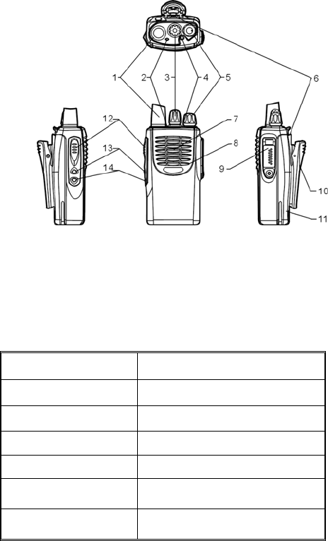
Brief Introduction
(1) Antenna
Used to transmit/receive signals.
(2) LED
Following table indicates LED indication and corresponding radio status.
LED Status
No display Standby
Green Receive
Red Transmit
Flashing green Scan
Flashing red Low battery voltage
Flashing orange Call waiting
(3) Channel Selector
Used to select wanted channel.
(4) Programmable key [A]
(5) Power/Volume Control Knob
Rotate the Power/Volume Knob clockwise until a “click” is heard to turn the radio on, fully
counter clockwise to turn the radio off. When the radio is on, turn the knob to adjust
volume.
(6) Battery Latch
Used to fasten the battery.
(7) Speaker
Used to output sounds.
(8) Microphone
Used to input sounds.
(9) External Jack
Used to connect with external earphone or programming cable.
(10) Belt Clip
Used to clip the radio on your belt.

4
(11) Battery Pack
(12) PTT key
Press and hold PTT, radio operates in transmit mode. Release PTT, radio returns to
receive mode.
(13) Programmable Key [B]
(14) Programmable Key [C]
The following table shows the key function when briefly pressed, pressed and held or
held down:
Key function
Key Function Briefly Press Press and Hold Hold Down
Emergency Siren Enable emergency siren Disable emergency siren -
Monitor - - Monitor
Scan Enable/Disable scan Enable/Disable scan -
Nuisance Delete Delete nuisance channel
in scan
Delete nuisance channel in
scan -
Select High/Low
Power Select High/Low Power Select High/Low Power -
Repeater/Talk Around Select Repeater or Talk
Around Mode
Select Repeater or Talk
Around Mode -
Repeater/Reverse
Frequency
Select Repeater or
Reverse Frequency Mode
Select Repeater or
Reverse Frequency Mode -
Call Transmit a Call Transmit a Call -
Note: Please contact your dealer for more details about programmable keys.
5
Radio Modes
Radio Feature Description
1. CTCSS/CDCSS/2-Tone/5-Tone
2. Channel Spacing 25KHz/12.5KHz (Wide/Narrow)
3. Programmable key
4. Squelch Tail Elimination
5. Priority Channel Scan/Nuisance Delete
6. Busy Channel Lockout
7. High/Low Power
8. Emergency Siren
9. Repeater/Talk Around
10. Call
11. TOT
12. VOX
13. Battery Save
14. Low Battery Alert
15. Voice Compression and Expansion
16. Software Upgrade
17. Wired Clone
18. PC Mode
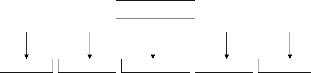
Frame of Radio Modes
Entry for Mode Startup
User Mode
Turn the power on to enter user mode. This mode is for normal operation.
Clone Mode
1) Connect the two radios with the clone cable. Turn the power on while holding down PTT
and programmable key B simultaneously. After two seconds, a BEEP sounds and LED
glows orange indicating that the radio enters clone mode.
2) In clone mode, pressing programmable key B can begin wired clone. MCU transmit data
Power On
User Mode Clone Mode PC Mode Adjustment Mode All Reset Mode
6
directly through UART port. During cloning, LED of source radio flashes red and that of
target radio flashes green. A BEEP sounds when cloning is complete.
PC Mode
1) Connect the radio with a PC by programming cable. And then turn the power on. The radio
enters PC mode after two seconds and LED glows orange.
2) Data can be transferred between MCU and PC via UART port. If data is transferred to the
radio from PC, it can be programmed into the EEPROM by MCU and LED flashes red during
data transfer. If data is transferred to PC from the radio, MCU sends the EEPROM data to PC
and LED flashes green during data transfer.
3) You can update software and provide second development feature for the user via PC
update programme. LED flashes orange during programme download.
4) To exit PC mode and enter conventional mode or other mode, turn on the power again.
All Reset Mode
Turn on the power while holding down PTT and programmable key A simultaneously (or short
circuit the two SELF points) to enter all reset mode. The EEPROM data is all reset. A BEEP
sounds and LED glows orange when All Reset is complete.
Adjustment Mode
Turn the power on while holding down PTT and programmable key C, after two seconds, the
radio enters adjustment mode. LED glows orange. Rotate channel selector knob to select
corresponding test item. Hold down A key to switch between wideband and narrowband.
Briefly press A key to save data. Press B key to adjust upwards and C downwards. Press PTT
to transmit or switch among center, low and high frequency.
CH1-CH16 are defined as following:
CH1: Transmitting VCO;
CH2: Receiving VCO;
CH3: Frequency Accuracy;
CH4: High power;
7
CH5: Low power;
CH6: CDCSS balance;
CH7: Maximum frequency deviation;
CH8: MIC sensitivity;
CH9: CTCSS deviation;
CH10: CDCSS deviation;
CH11: FFSK deviation;
CH12: TONE deviation;
CH13: Receiving sensitivity;
CH14: Squelch level;
CH15: Low battery alert level;
CH16: VOX sensitivity.
8
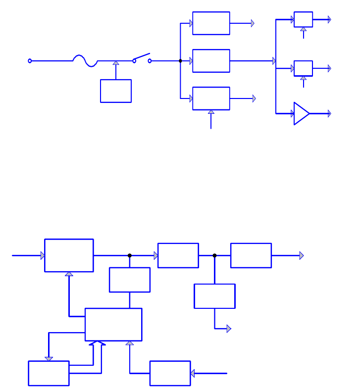
Circuit Description
1. Power Supply
Power supply of the radio is derived from the battery, which supplies battery B+ after
passing through fuse 3A and then feeds through power switch. The power supplies
voltage for three AVRs. IC505 supplies 5V (5M) voltage for the control circuit. IC9
supplies 5V (5C) voltage for the shared circuit. And IC6 supplies voltage for the
transmit/receive circuit. In transmit mode, 5TC becomes low voltage and Q3 is turned
on to supply 5V(5T) voltage for the transmit circuit. In receive mode, 5RC becomes
low voltage and Q2 is turned on to supply 5V (5R) voltage for the receive circuit.
BATT FUSE
PROTECT 5C
5M
BUFF
1/2BIA
S
AVR
AVR
SW
5R
5T
AVR
SW
SW
SAVE
5RC
5TC
Fig. 1 Power Supply Block Diagram
2. PLL Frequency Synthesizer
PLL circuit generates the first local oscillator signal for reception and RF signal
for transmission.
CPU
Q416
UL
X401
IC400
PLL
IC500
CV
CLK,DAT,EN TCXO
VCO BUFF SW
MB
D100
T/R
To Drive Amp
BUFF D103
SW
To Mixer
Q310
Fig2. PLL circuit
1) PLL
IC400 is fractional divider. Step frequency of PLL circuit is 2.5KHz or 6.25KHz. A
16.8MHz reference oscillator signal is divided at IC400 by a fixed counter to
generate a 20KHz or 50KHz reference frequency. Output signal from VCO is buffer
amplified by Q416 and divided at IC400 by a frequency divider. Divided signal is
compared in the phase comparator with 20KHz or 50KHz reference signal of IC400.
9
Output signal from phase comparator is filtered through a low pass filter and passed
to the VCO to control oscillator frequency.
2) VCO
The operating frequency is generated by Q352 in transmit mode and by Q350 in
receive mode. Operating frequency generates a control voltage by phase
comparator to control varactor diodes so that the oscillator frequency is the same as
the MCU preset frequency (D350, D352, D354 and D355 in transmit mode and D351,
D353, D356 and D357 in receive mode). T/R pin is set high level in receive mode
and low in transmit mode. The output from Q352 and Q350 is amplified by Q354 and
sent to buffer amplifier.
3) Unlock Detector
An unlock condition appears if low level appears at LOCK pin of IC400.
Transmission is forbidden if this condition is detected by microprocessor.
3. Receiver
The receiver utilizes double conversion superheterodyne.
C
ANT
ANT
SW
BPF Q201
RF AMP BPF MCF
XF201 IF AMP
Q222
MIXER
IC218
CF201,202
IF,MIX,DET
IC204
AF AMP
IC720 SP
1st Local OSC
(PLL) 2nd Local OSC
IF AMP
Q216
Fig.3 Receiver Section Configuration
1) Front-end Amplifier
The signal from antenna is amplified at RF amplifier (Q201) after passing
through a transmit/receive switch circuit and a band pass filter. The amplified
signal is filtered through a band pass filter to remove unwanted signals before
it passes the first mixer.
2) First Mixer
The signal from RF amplifier is mixed with the first local oscillator signal from PLL
frequency synthesizer circuit at the first mixer (IC218) to create a 44.85MHz first IF
signal. The first IF signal is then fed through a crystal filter (XF201) to further remove
spurious signals from adjacent channel.
3) IF Amplifier
The first IF signal is amplified by Q216 before passing through crystal filter and by
Q222 after crystal filter and then enters IF processing chip IC204. The signal is mixed
with the second local oscillator signal again in IC204 to create a 455KHz second IF
signal. The second IF signal then passes through a 455KHz ceramic filter (wideband:
CF201/narrowband: CF202) to eliminate unwanted signals before it is amplified and
detected in IC204.
4) Narrowband/Wideband Switch Circuit
Turn on ceramic filter CF201 (wideband)/CF202 (narrowband) to set each channel as
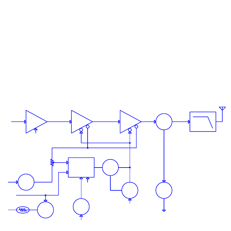
10
wideband or narrowband. W/N pin of IC500 outputs wideband (high level) and
narrowband (low level) signal.
5) AF Amplifier
The result AF signal from IC204 is amplified by IC606, and then passes through AF
processing chip IC601 and compander IC603. The processed AF signal is then
amplified by an AF power amplifier (IC720) to drive the speaker.
4. Transmitter
1) AF and Signaling
Modulating signal from the microphone passes through Q700 switch and compander
IC603 before it enters AF processing chip IC601. Under the control of MCU, IC601
produces DTMF/CTCSS/CDCSS/2-Tone/5-Tone signaling, which then pass through
MOD and enter VCO together with the modulating signal for direct FM modulation.
(See fig.5)
2) RF Amplifier
The transmit signal from VCO buffer amplifier (Q310) is amplified by Q101 and Q102.
The amplified signal is then amplified by the power amplifier Q105 and Q107
(include a two-stage FET amplifier) to create 4.0W RF power. (See fig.4)
D
C
B
A
Title
AMP
Q101.102
5T
DRIVE AMP
Q105
FINAL AMP
Q107
ANT SW
D101 LPF
ANT
ANT SW
D201.202
RX
Q106
SW
Q109
SW
5T
IC100
APC
DET
Q103.Q104
B SW
B
APC
5T
TH101
SW
Q110 5T
Q108
SW 5TC
Fig.4 APC System
3) Antenna Switch and LPF
Output signal from RF amplifier passes through a low-pass filter network and a
transmit/receive switch circuit comprised of D101, D201 and D202 before it reaches
the antenna terminal. D201 and D202 is turned on (conductive) in transmit mode and
off (isolated) in receive mode.
4) APC
The automatic power control (APC) circuit stabilizes the transmit output power by
detecting the drain current of final stage amplifier FET. IC100 (2/2) compares the
preset reference voltage with the voltage obtained from final current. APC voltage is
proportional to the difference between auto detect voltage and reference voltage
11
output from IC100 (1/2). The output voltage controls FET power amplifier and keeps
the transmitter output power constant. The output voltage can be varied by the
microprocessor, which hence controls the transmitter output power.
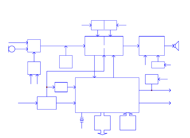
5. Signalling Section
The block diagram of signaling section is shown as figure 5.
D601
LIMITTER
X601
BASEBAND PROCESSOR
IC601
BBP_IRQN
BBP_RPL
SP
MIC SW
Q700 AF PA
IC710
SW
Q710
MIC
AUDIO_EN
EXT_SPK+
EXT_MIC
BBP_CSN
BBP_CMD
BBP_CLK
Q701
SW
EXT_MIC_SEL
EXT_SP_SEL
IC605
BUFFER Ver
Vbias
COMPANDER
IC603
SW
COM_SW EXP EXP_SW
IC604
MOD
MB
COMPRESSOR EXPANDER
AF PA
MIC_FB
AUDIO
SW
COM
IC606
BUFF AMP
Vbias
IC611
FILTER
AF DET
Fig.5 AF and Signalling Circuit
In the transmit section, signallings (CTCSS, CDCSS, DTMF, 2-Tone and 5-Tone) are
produced by IC601 under the control of MCU and enter VCO together with AF signal
from MIC for modulation.
In the receive section, after buffer amplified together with IF demodulation signals,
the signallings enter IC601 for decode. The decoded data is then sent to MCU for
recognition.
6. Control System
The IC500 CPU operates at 9.8304MHz.
The block diagram of MCU control system is shown as following:
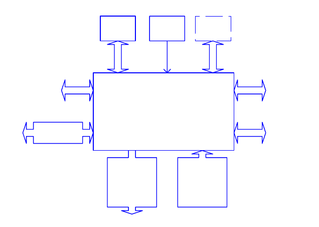
12
MCU
SAVE
APC/TV
BATT Det
VOL Level
CH Encode
5TC
5RC
W/N
MUTE
T/R
BEEP
LED
AP SW I/E
RSSI
PTT
KEY SW
TXD/RXD
CTC/CDC Codec
E2PROM FLASH
AF Processor
PLL IC
RESET
Fig.6 MCU Block Diagram
Circuit in this section is mainly comprised of MCU, EEPROM, FLASH and reset IC etc.
MCU control circuit accomplishes the following functions: accomplish the reset
initialization according to the programmed feature of the radio when power on; detect
key signal and monitor battery voltage; send necessary frequency data to PLL
according to encode of the channel; switch and control transmit/receive according to
the signal input from PTT; turn on/off the mute circuit according to the input signaling
decode signal and squelch level signal; output control signal to control the light/off of
LED; output BEEP signal to drive the speaker.

13
CPU Pins
No. Port Name I/O Feature Description
1 P94 O Ver Frequency accuracy adjustment
2 P93 O APC/TV Transmit power/receiving sensitivity adjustment
3 P92 I Key1 NC
4 P91 I External option judgement NC
5 P90 I SELF
All reset mode control; ground this pin to enter all reset
mode
6 BYTE I VCC 8 bit external data bus
7 CNVSS I GND MCU operates in single-chip mode after reset
8 P87 I Key2 NC
9 P86 I Key3 NC
10 RESET I Reset IC MCU reset when low level is input
11 Xout O Crystal oscillator output 9.8304M crystal oscillator
12 Vss I GND Ground
13 Xin I Crystal oscillator input 9.8304M crystal oscillator
14 Vcc I VCC Power supply
15 P85 I NMI Connect with high level
16 P84 I EN0 Channel selector knob input
17 P83 I SW1 A key
18 P82 I BBP_IRQN CMX881 interrupt output
19 P81 I BBP_RPL CMX881 data output
20 P80 O BBP_CLK CMX881 clock input
21 P77 O BBP_CMD CMX881 data input
22 P76 O BBP_CSN CMX881data enable, low level: Enable
23 P75 O AUDIO_EN AF amplifier control H: Enable L: Standby
24 P74 O COM_SW Compressor enable H: Enable L: Disable
25 P73 O EXP_SW Expander enable H: Enable L: Disable
26 P72 O W/N Narrowband/wideband H: Wideband L: Narrowband
27 P71 I/O EEPROM_DATA EEPROM data
28 P70 O EEPROM_CLOCK EEPROM clock input
29 P67 O NULL NC
30 P66 O NULL NC
31 P65 I LOCK PLL unlock detect H: PLL lock L: PLL unlock
32 P64 O PLL_EN PLL IC strobe
33 P63 O TXD Serial data output
34 P62 I RXD Serial data input
35 P61 I Key4 NC
36 P60 I External option judgement NC
37 P57 O VCC Clock output, connected to high level (Null)
38 P56 NULL NC
39 P55 I VCC HOLD pin, connected to high level (Null)

14
40 P54 NULL NC
41 P53 NULL NC
42 P52 O OE Flash data output enable, active low
43 P51 NULL NC
44 P50 O WE Flash data input enable, active low
45 P47 I OPTION2 External accessory select
46 P46 I OPTION1 External accessory select
47 P45 O T/R
Transmit/receive PLL select
H: receive L: transmit
48 P44 O CE Flash chip select, active low
49 P43 NULL NC
50 P42 O A18 Flash address
51 P41 O A17 Flash address
52 P40 O A16 Flash address
53 P37 O A15 Flash address
54 P36 O A14 Flash address
55 P35 O A13 Flash address
56 P34 O A12 Flash address
57 P33 O A11 Flash address
58 P32 O A10 Flash address
59 P31 O A9 Flash address
60 Vcc I VCC
61 P30 O A8 Flash address
62 Vss I GND
63 P27 O A7 Flash address
64 P26 O A6 Flash address
65 P25 O A5 Flash address
66 P24 O A4 Flash address
67 P23 O A3 Flash address
68 P22 O A2 Flash address
69 P21 O A1 Flash address
70 P20 O A0 Flash address
71 P17 I SW3 C key
72 P16 I SW2 B key
73 P15 I PTT PTT key
74 P14 O LR Red LED control H: light L: off
75 P13 O LG Green LED control H: light L: off
76 P12 O SAVE Battery save control H: off L: on
77 P11 O 5TC
Transmit circuit power supply control
H: off L: on
78 P10 O 5RC
Receive circuit power supply control
H: off L: on

15
79 P07 I/O D7 Flash data
80 P06 I/O D6 Flash data
81 P05 I/O D5 Flash data
82 P04 I/O D4 Flash data
83 P03 I/O D3 Flash data
84 P02 I/O D2 Flash data
85 P01 I/O D1 Flash data
86 P00 I/O D0 Flash data
87 P107 I EN3 Channel selector knob input
88 P106 I EN2 Channel selector knob input
89 P105 I EN1 Channel selector knob input
90 P104 I CTCSS_IN CTCSS input
91 P103 I BATTD Low battery level detect (analogue)
92 P102 I SQL Squelch level input (analogue)
93 P101 I RSSI RSSI detect pin (analogue)
94 Avss I VCC A/D conversion power supply input
95 P100 I VOL Volume knob input (analogue)
96 Vref I VCC Battery detect reference voltage
97 Avcc I VCC A/D conversion power supply input
98 P97 NULL NC
99 P96 O PLL_DATA PLL IC data input
100 P95 O PLL_CLK PLL IC clock

16
Adjustment Description
Required Test Instrument
Radio communication test set 1 set
Scanner 1 set
3A/10V power supply 1 set
Digital voltmeter 1 set
3A Ammeter 1 set
Preparation
Open the programming software in PC and operate as the following instructions.
1. Programme Download:
Connect the radio with the computer via programming cable. And then turn the power on. LED
glows red. Click “Programme” → “Download” on the interface to choose programme. Click
“Open” to begin download and LED flashes red. When download is complete, click “End” and
turn the power off. And then disconnect the programming cable.
2. Initialization:
Turn the power on while holding down [PTT] and [A] key simultaneously. LED glows orange
and a BEEP sounds. Radio channel frequency and setting data are initialized.
3. Destination Set:
Connect the radio with the computer via programming cable. And then turn the power on. LED
glows red. Set “frequency range” on the programming software interface. And then click
“Programme” → “ Writing”.
4. Factory Setting
The compander is open. Squelch level 2. Adjustment mode is disabled.
Adjustment
VCO
Measurement Adjustment
Item Condition
Test
Instrument Terminal Part Method
Specification/
Remarks
1. Setting Power supply 7.5V
1.Turn to CH1. Press
PTT. TX High Check 3.3V±0.2V
2.Transmit
VCO loc
k
voltage 2. Press PTT again.
TX Low Check 1.0V±0.4V
1. Turn to CH2. Press
PTT. TX High Check 3.1V±0.2V 3. Receiving
VCO loc
k
voltage 2. Press PTT again.
TX Low
Digital
Voltmeter CV TC350
TC351
Check 1.0V±0.4V

17
Transmitter
Measurement Adjustment
Item Condition
Test Instrument Terminal Part Method
Specification
/Remarks
1. Transmit
frequency
Turn to CH3.
Press PTT.
Radio
Communication
Test Set
ANT [B] (up)
[C] (down)
A
djust to cente
r
frequency. Press
[A] to save.
Error≤
150Hz
1. Turn to CH4.
Press PTT.
Center frequency
A
djust to 4.0 W,
I≤1.6A.
Press [A] to save.
2. Press PTT.
Frequency changes to
low frequency.
A
djust to 4.0 W,
I≤1.6A.
Press [A] to save.
High
3. Press PTT again.
Frequency changes to
high frequency.
A
djust to 4.0 W,
I≤1.6A.
Press [A] to save.
4.0W±0.3W
4.0W±0.3W
1. Turn to CH5.
Press PTT.
Center frequency.
A
djust to 1.0 W,
I≤0.7A.
Press [A] to save.
2. Press PTT.
Frequency changes to
low frequency.
A
djust to 1.0 W,
I≤0.7A.
Press [A] to save.
2. Power
Low
3. Press PTT again.
Frequency changes to
high frequency.
Radio
Communication
Test Set
Ammeter
ANT [B] (up)
[C] (down)
A
djust to 1.0 W,
I≤0.7A.
Press [A] to save.
1W±0.3W
1. Turn to CH6.
Press PTT.
The radio operates
with wideband.
Center frequency.
2. Press PTT.
Frequency changes to
low frequency.
3.
CDCSS
balance
Wideba-
nd
Narrow-
band
3. Press PTT again.
Frequency changes to
high frequency.
Radio
Communication
Test Set
LPF: 15KHz
ANT [B] (up)
[C] (down)
Rectify the
waveform to
square wave.
Press [A] to
save.

18
4. Press [A] for two
seconds. LED flashes
indicating that the
radio operates with
narrowband.
Center frequency.
A
djust narrowband
following the above
steps.
Wideba-
nd
1. Turn to CH7.
Press PTT.
The radio operates
with wideband.
Center frequency.
A
djust it to
4.0KHz±100Hz.
Press [A] to save.
4.
Maximu-
m
frequenc
-y
deviation
Narrow-
band
2. Press [A] for two
seconds. LED flashes
indicating that the
radio operates with
narrowband.
Center frequency.
Radio
Communication
Test Set
LPF: 15KHz
AF: 1KHz 1V
ANT
MIC Jack
[B] (up)
[C] (down)
A
djust it to
2.0KHz±100Hz.
Press [A] to save.
5. MIC Sensitivity
Turn to CH8.
Press PTT.
The radio operates
with wideband.
Center frequency.
Radio
Communication
Test Set
LPF: 15KHz
AF: 1KHz 24mV
ANT
MIC Jack
[B] (up)
[C] (down)
Check frequenc
y
deviation
2.9±0.1KHz.
Press [A] to save.
A
djust as
wideband.
1. Turn to CH9.
Press PTT.
The radio operates
with wideband.
Center frequency.
2. Press PTT.
Frequency changes to
low frequency.
Wideba-
nd
3. Press PTT again,
frequency changes to
high frequency.
A
djust deviation
to 0.70KHz ±
50Hz.
Press [A] to save.
6.
CTCSS
deviation
Narrow-
band
4. Press [A] for two
seconds. LED flashes
indicating that the
radio operates with
narrowband.
High frequency.
Radio
Communication
Test Set
LPF: 3KHz
ANT [B] (up)
[C] (down)
Adjust deviation
to 0.35KHz±
50Hz.
Press [A] to save.

19
5. Press PTT.
Frequency changes to
center frequency.
6. Press PTT.
Frequency changes to
low frequency.
Wideba-
nd
Turn to CH10.
See CTCSS deviation
adjustment.
Adjust deviation
to 0.70KHz±
50Hz.
Press [A] to save.
7.
CDCSS
deviation
Narrowb
-and
See CTCSS deviation
adjustment.
Radio
Communication
Test Set
LPF: 3KHz
ANT [B] (up)
[C] (down) Adjust deviation
to 0.35KHz±
50Hz.
Press [A] to save.
Wideba-
nd
Turn to CH11.
See CTCSS deviation
adjustment.
Adjust deviation
to 3KHz±
0.1KHz.
Press [A] to save.
8.FFSK
deviation
Narrow-
band
See CTCSS deviation
adjustment.
Radio
Communication
Test Set
LPF: 3KHz
ANT [B] (up)
[C] (down) Adjust deviation
to 1.45KHz±
0.05KHz
Press [A] to save.
Wideba-
nd
Turn to CH12.
See CTCSS deviation
adjustment.
Adjust it to
3KHz±0.1KHz.
Press [A] to save.
9.TONE
deviation
Narrow-
band
See CTCSS deviation
adjustment.
Radio
Communication
Test Set
LPF: 3KHz
ANT [B] (up)
[C] (down)
A
djust it to
1.45KHz ±
0.05KHz
Press [A] to save.
10. Low battery
alert level
Turn to CH15. Adjust
voltage to 6.2V. Digital Voltmeter Press [A] to save.
11.VOX
Sensitivity
Turn to CH16.
Radio
Communication
Test Set
LPF:15KHz
A
F:1KHz 3mV
ANT
MIC Jack Press [A] to save.
20
Receiver
Measurement Adjustment
Item Condition Test Instrument Terminal Part Method
Specification/
Remarks
1. Turn to CH13.
Press PTT.
Center frequency.
2. Press PTT.
Frequency changes to
low frequency.
Sensitivity
3. Press PTT.
Frequency changes to
high frequency.
Scanner ANT
T1
[B] (up)
[C] (down)
Adjust the
waveform.
Press [A] to save.
1. Turn to CH14.
Press PTT.
The radio operates
with wideband.
Center frequency.
2. Press PTT.
Frequency changes to
low frequency.
Wideba-
nd
3. Press PTT.
Frequency changes to
high frequency.
Radio
Communication
Test Set
SSG output:
-118dBm
MOD: 1KHz
DEV: ±3KHz
FILTER:
0.3-3.4KHz
A
djust radio
communication
test set.
SSG output:
SINAD: 12dB
Press [A] to save.
4. Press [A] for two
seconds. LED flashes
indicating that the
radio operates with
narrowband.
High frequency.
5. Press PTT.
Frequency changes to
center frequency.
Squelch
Narrow-
band
6. Press PTT.
Frequency changes to
low frequency.
Radio
Communication
Test Set
SSG output:
-118dBm
MOD:1KHz
DEV:±1.5KHz
FILTER:
0.3-3.4KHz
ANT
Speaker Jack
A
djust radio
communication
test set.
SSG output:
SINAD: 12dB
Press [A] to save.
21
Disassembly and Assembly for Repair
Disassemble the radio
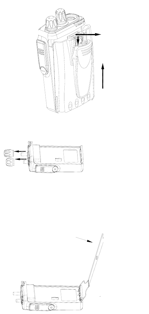
1. Turn off the radio.
2. Remove the battery: a. Press the release at top of the battery downwards.
b. Separate top of the battery from the radio.
c. Lift the battery off. (See fig.1)
电池推钮
Fig. 1
3. Remove the antenna.
4. Remove the knob. (See fig.2)
Fig. 2
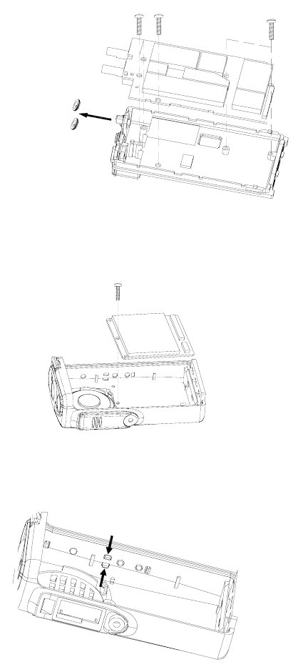
5. Separate the chassis from PCB:
a. Insert a screwdriver (Material No. 99050312) into the clearance between chassis and
the case.
b. Push the screwdriver downwards to separate the chassis from the case.
c. Lift the bottom of the chassis and pull it out of the PCB. (See fig.3)
Fig.3
Battery Latch
22
6. Remove the main PCB: a. Remove the two screw caps on top of the unit.
b. Remove the five screws between PCB and the chassis.
c. Loosen the weld between antenna pedestal and PCB
using a soldering iron.
d. Lift the PCB off. (See fig.4)
Fig.4
7. Remove the small PCB: Loosen the screw to remove the small PCB. And then loosen
the socket of flexible PCB. (See fig.5)
Fig.5
8. Disassemble PTT key: Push the tab on PTT out of the hole on the case to disassemble
PTT key. (See fig.6)
Fig.6
Assemble the radio
1. Attach PTT: Align the tab on PTT with the corresponding hole on the case.
(See fig.7)
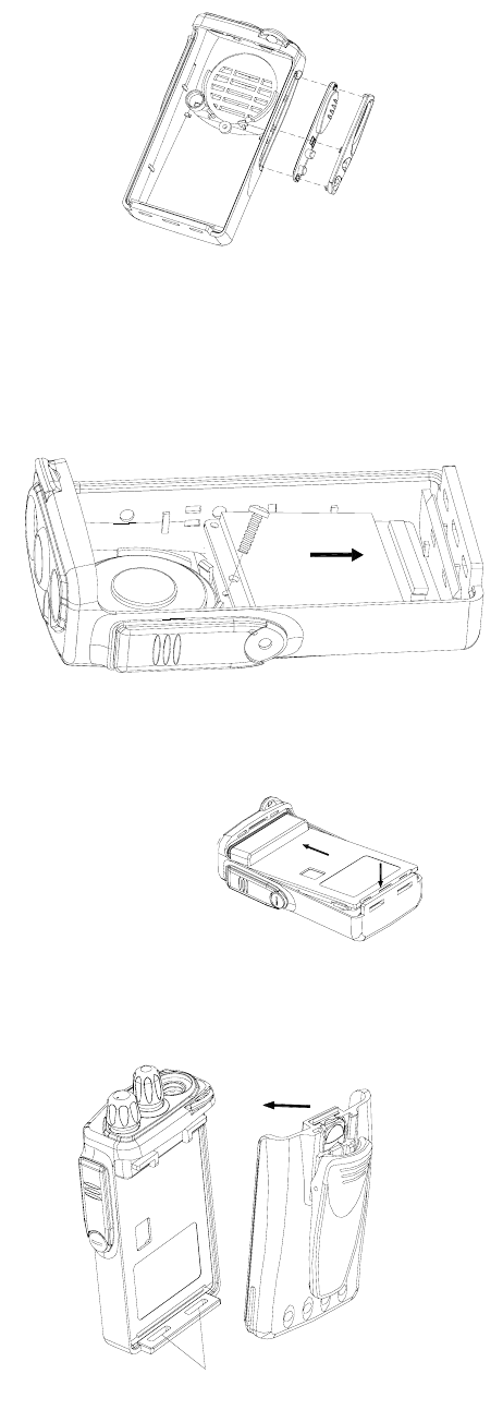
23
Fig.7
2. Assemble the small PCB:
a. Insert the flexible PCB into the socket on the small PCB and lock it up.
b. Insert the bottom of the small PCB into the underside of the two tabs under the
case.
c. Tighten the screws. (See fig.8)
Fig.8
3. Assemble the chassis and PCB
a. Insert the switch shaft in front of the PCB into the corresponding holes on the case.
b. Press the bottom of the chassis downwards until a click is heard. (See fig.9)
Fig.9
4. Attach the battery:
a. Insert the two extensions at the bottom of the battery into the two slots on the case.
b. Press the top of the battery toward the radio until a click is heard. (See fig.10)
Fig.10
Slot
24
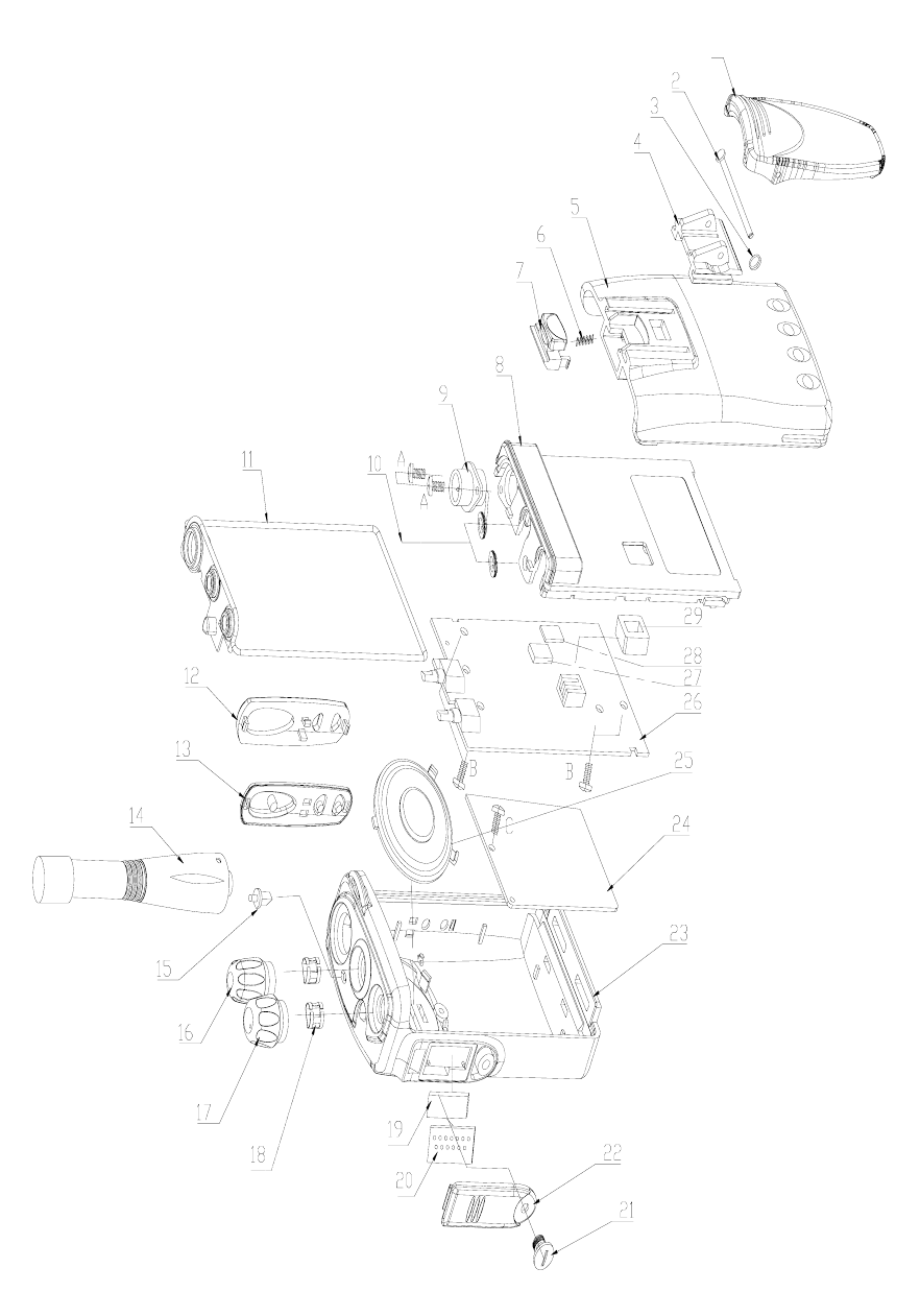
Exploded View
25
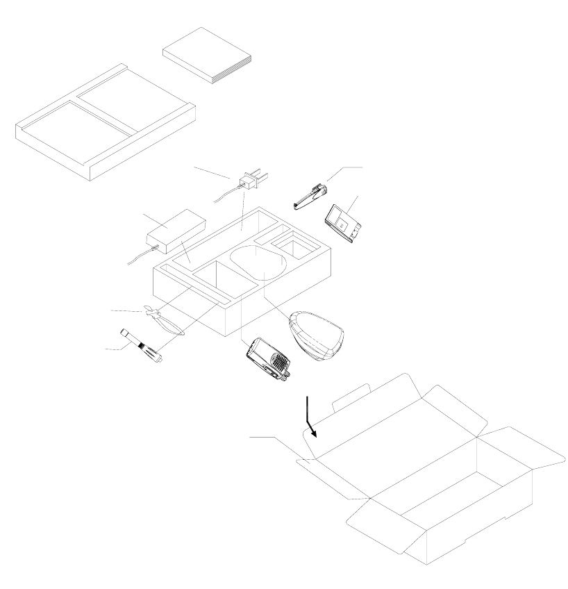
Packing
Owner ' s Manual
Belt Clip
Battery
Adapt er
Char ger
Gift Box
St r ap
Ant enna
Mai n Uni t
Power Suppl y Cor d

26
Specification
Item Specification
Frequency Range 400~430MHz 440~470MHz 145~175MHz
Channel Number 16
Channel Spacing 25KHz/12.5KHz
Frequency Stability ±2.5ppm
IF Frequency 44.85MHz/455KHz
Antenna Impedance 50Ω
Speaker Impedance 24Ω
Operation Voltage 7.2V
Operating Temperature -20~+50ºC
Receiver
Sensitivity 0.25uV (Wide)/0.35uV (Narrow)
S/N 45 (Wide) /40dB (Narrow)
Modulation Acceptance 2*7.5KHz/2*3.5KHz
Adjacent Channel Selectivity 70dB (Wide) /60dB (Narrow)
Co-channel Rejection -8dB (Wide) /-12dB (Narrow)
Blocking 85dB
Spurious Response 70dB
Intermodulation Rejection 65dB
Audio Response From 6 dB/oct. De-Emphasis. +2dB -6dB
AF Power 500mW
Audio Distortion 5%
Transmitter
Carrier Frequency Error ±2.5ppm
Output Power 4W±0.5 (High)/1W±0.2 (Low)
Modulation Limit 5K (Wide)/2.5K (Narrow)
Adjacent Channel Power 70dB (Wide)/60dB (Narrow)
Modulate Sensitivity 24±3mV
Modulate Distortion 3% (Wide) /5% (Narrow)
Audio Response From 6dB/oct. Pre-Emphasis ±3dB
Residual Frequency Modulation 45dB (Wide) /40dB (Narrow)
Conducted Spurious Emission -70dB/-36dBm
Transmit Current 1.6A/0.7A