Hanbit Electronics HANBIT-CFC Internet Phone User Manual
Hanbit Electronics Co., LTD. Internet Phone Users Manual
UserManual.wiki
>
Hanbit Electronics
>
HANBIT CFC User Manual
Users Manual
Navigation menu
Upload a User Manual
Namespaces
Wiki Guide
HTML
PDF
Info
Views
User Manual
Discussion / Help
Navigation
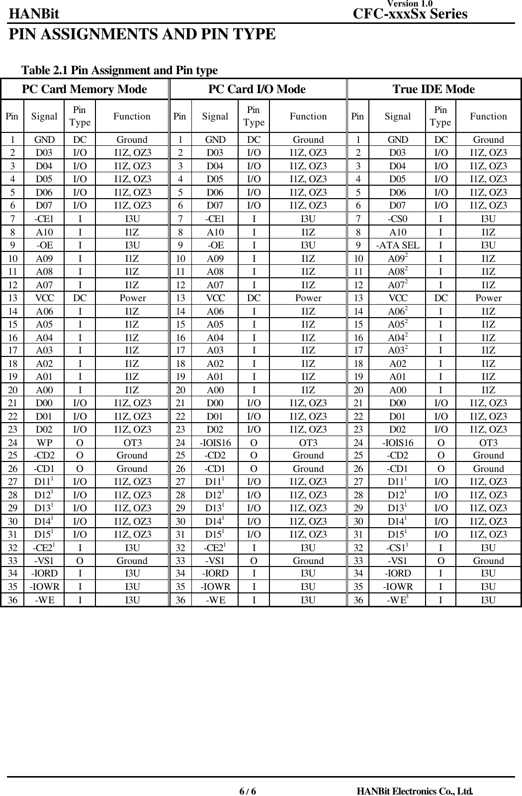
![Version 1.0 HANBit CFC-xxxSx Series 8 / 8 HANBit Electronics Co., Ltd. Table 2.2 Signal Descriptions Signal Name Dir. Pin Description A10 - A0 (PC Card Memory Mode) A10 - A0 (PC Card I/O Mode) A2 - A0 (True IDE Mode) I I 8,10,11,12,14,15,16, 17,18, 19,20 18,19, 20 These address lines along with the -REG signal are used to select the following: The I/O port address registers within the CompactFlash Storage Card or CF+ Card, the memory mapped port address registers within the CompactFlash Storage Card or CF+ Card, a byte in the card's information structure and its configuration control and status registers. This signal is the same as the PC Card Memory Mode signal. In True IDE Mode only A[2:0] are used to select the one of eight registers in the Task File, the remaining address lines should be grounded by the host. BVD1 (PC Card Memory Mode) -STSCHG (PC Card I/O Mode) Status Changed -PDIAG (True IDE Mode) I/O 46 This signal is asserted high as BVD1 is not supported. This signal is asserted low to alert the host to changes in the RDY/-BSY and Write Protect states, while the I/O interface is configured. Its use is controlled by the Card Config and Status Register. In the True IDE Mode, this input / output is the Pass Diagnostic signal in the Master / Slave handshake protocol. BVD2 (PC Card Memory Mode) -SPKR (PC Card I/O Mode) -DASP (True IDE Mode) I/O 45 This signal is asserted high as BVD2 is not supported. This line is the Binary Audio output from the card. If the Card does not support the Binary Audio function, this line should be held negated. In the True IDE Mode, this input/output is the Disk Active/Slave Present signal in the Master/Slave handshake protocol. -CD1, -CD2 (PC Card Memory Mode) -CD1, -CD2 (PC Card I/O Mode) -CD1, -CD2 (True IDE Mode) O 26,25 These Card Detect pins are connected to ground on the CompactFlash Storage Card or CF+ Card. They are used by the host to determine that the CompactFlash Storage Card or CF+ Card is fully inserted into its socket. This signal is the same for all modes. This signal is the same for all modes. -CE1, -CE2 (PC Card Memory Mode) Card Enable -CE1, -CE2 (PC Card I/O Mode) Card Enable -CS0, -CS1 (True IDE Mode) I 7,32 These input signals are used both to select the card and to indicate to the card whether a byte or a word operation is being performed. -CE2 always accesses the odd byte of the word. –CE1 accesses the even byte or the Odd byte of the word depending on A0 and -CE2. A multiplexing scheme based on A0, -CE1, -CE2 allows 8 bit hosts to access all data on D0-D7. This signal is the same as the PC Card Memory Mode signal. In the True IDE Mode CS0 is the chip select for the task file registers while CS2 is used to select the Alternate Status Register and the Device Control Register. Signal Name Dir. Pin Description -CSEL (PC Card Memory Mode) -CSEL (PC Card I/O Mode) -CSEL I 39 This signal is not used for this mode. This signal is not used for this mode. This internally pulled up signal is used to configure this device as a Master](https://usermanual.wiki/Hanbit-Electronics/HANBIT-CFC/User-Guide-183271-Page-8.png)