Hanbit Electronics HANBIT-CFC Internet Phone User Manual
Hanbit Electronics Co., LTD. Internet Phone Users Manual
Users Manual

Version 1.0
HANBit CFC-xxxSx Series
1 / 1 HANBit Electronics Co., Ltd.
1. PRODUCT OVERVIEW
GENERAL DESCRIPTION
The CFCxxxSx series CompactFlash card is a flash technology based with ATA interface flash
memory card. It is constructed with flash disk controller chip and NAND-type (Samsung) flash memory
device. The CompactFlash card operates in both 3.3-Volt and 5.0-Volt power supplies. It comes in
capacity of 16, 32, 64, 96, 128, 192, 256, 384 MB and up to 512 MB formatted for type-I card.
By optimizing flash memory management, the life of this card can be extended to its maximum level.
Because the ECC function is included, the correctness of data transfer between the card and the mobile
device can be guaranteed. The power down and sleep modes of the card can ensure longer life of the
batteries in the mobile devices. It is a perfect choice of solid-state mass-storage cards for battery backup
handheld devices such as Digital Camera, Audio Player, PDA, GPS, or the applications which require high
environment tolerance with high performance sustained write speed.
FEATURES
- ATA / True IDE compatible host interface
- ATA command set compatible
- Very high performance, very low power consumption
- Automatic error correction
- Support 3 power save mode : stop/idle/active
- Support for CIS implemented with 256 bytes of attribute memory
- Support for 8 or 16 bit host transfers
- 3.3V/5.0V operation voltage
- Host data transfer rate : 20MB/s
- Flash data transfer rate : 10MB/s
- Host Interface bus width : 8/16 bit Access
- Flash Interface bus width : 8 bit Access
- Capacity : Min. 16MB ~ Max. 512MB
- MTBF : 1,000,000 hours, minimum 30,000 insertions
- Operating vibration : 15G peak to peak maximum
- Operating shock : 1,000G maximum
PRODUCT SPECIFICATIONS
Capacities :
Compact Flash Card Min.16MB ~ Max.512MB, ATA/IDE Interface Mode,
Support 3 power save mode, 3.3V/5.0V Operating Part No. CFCxxxSx

Version 1.0
HANBit CFC-xxxSx Series
2 / 2 HANBit Electronics Co., Ltd.
16, 32, 48, 64, 96, 128, 192, 256, 384 and up to 512 MB (formatted)
System Compatibility :
Please refer to the compatibility list of index.
Performance :
Data Transfer Rates : up to 4.2 MB/s in ATA PIO mode 4
To/from Flash memory : up to 12.4 MB/s
To/from host : up to 20MB/s
Sustained write : up to 2.9MB/s in ATA PIO mode 4
Sustained read : up to 5.62MB/s in ATA PIO mode 4
Operating Voltage : 3.3V / 5.0V ± 10%
Power consumption :
Read mode 30 mA (typ), 40 mA (Max)
Write mode 30 mA (typ), 40 mA (Max)
Stop mode 30 µA (typ)
Environment conditions :
Operating temperature 0°C to + 65°C
Storage temperature - 20°C to + 70°C
Relative humidity 95%(Max)
Dimension :
Weight Capacity dependent
Length 36.4 ± 0.15 mm (1.433 ± 0.006 in.)
Width 42.8 ± 0.10 mm (1.685 ± 0.004 in.)
Thickness 3.3 mm ± 0.10 mm (0.130 ± 0.004 in.)
Version 1.0
HANBit CFC-xxxSx Series
3 / 3 HANBit Electronics Co., Ltd.
ELECTRICAL SPECIFICATIONS
Table 1.1 Absolute Maximum Ratings
Symbol Parameter Ratings Unit
VDD Supply voltage - 0.3 to + 7.0 V
VIN Input voltage - 0.3 to + 7.0 V
IIN DC input current - 10 mA
TSTG Storage temperature - 20 to + 85 °C
Table 1.2 Recommended Operating Conditions
Symbol Parameter Ratings Unit
5V 4.75 to 5.25 V
VDD DC Supply voltage 3.3V 3.0 to 3.6 V
Ta Storage temperature - 20 to +70 °C
Table 1.3 DC Characteristics
(Ta=0°C to 70°C, VDD=3.0 to 5.3V)
Symbol Parameter Min. Typ. Max. Unit
IDD Operating Current 30 70 mA
Ids Stop Current 50 150 µA
VDD High Level Output Voltage 2.4 V
VDD Low Level Output Voltage 0.4 V
Version 1.0
HANBit CFC-xxxSx Series
4 / 4 HANBit Electronics Co., Ltd.
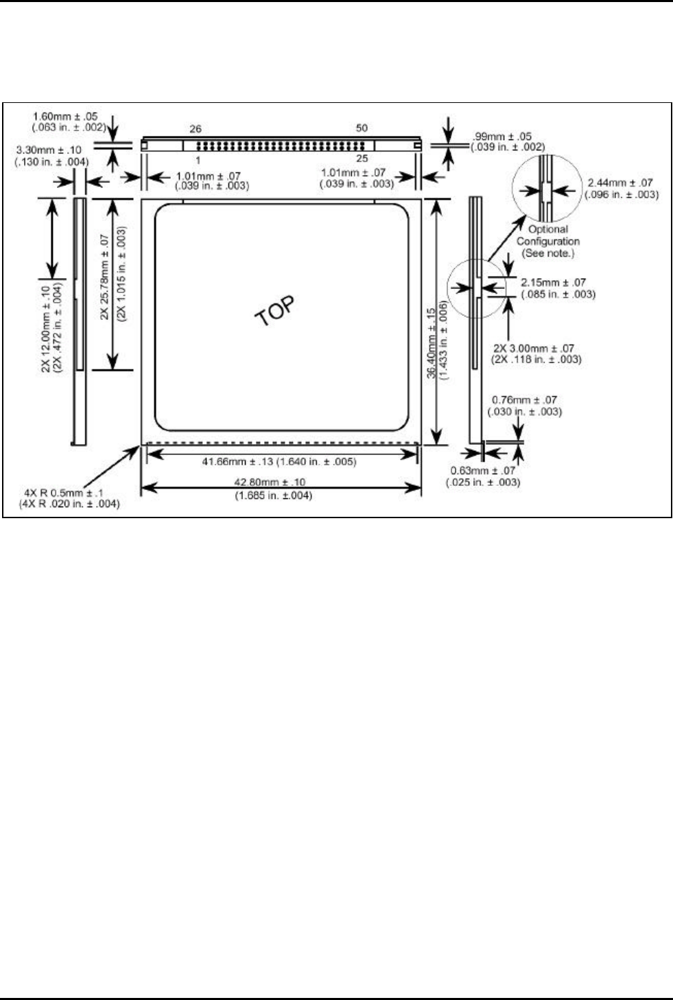
PHYSYCAL SPECIFICATION
Note: The optional notched configuration was shown in the CF Specification
Rev. 1.0. In specification Rev. 1.2, the notch was removed for ease of tooling.
This optional configuration can be used but it is not recommended.
Figure 1.1 Type I CompactFlash Storage Card Dimensions

Version 1.0
HANBit CFC-xxxSx Series
5 / 5 HANBit Electronics Co., Ltd.
Electrical Interface
Physical Description
The host is connected to the CompactFlash Storage Card or CF+ Card using a standard 50-pin
connector. The connector in the host consists of two rows of 25 male contacts each on 50 mil
(1.27 mm) centers.
Pin Assignments and Pin Type
The signal/pin assignments are listed in Table 4. Low active signals have a “-” prefix. Pin types are
Input, Output or Input/Output. Section 4.3 defines the DC characteristics for all input and output
type structures.
Electrical Description
The CompactFlash Storage Card functions in three basic modes:
1) PC Card ATA using I/O Mode
2) PC Card ATA using Memory Mode
3) True IDE Mode
Which is compatible with most disk drives. CompactFlash Storage Cards are required to support
all three modes. The CF Cards normally function in the first and second modes, however they can
optionally function in True IDE mode. The configuration of the CompactFlash Card will be
controlled using the standard PCMCIA configuration registers starting at address 200h in the
Attribute Memory space of the storage card or for True IDE Mode, pin 9 being grounded. The
configuration of the CF Card will be controlled using configuration registers starting at the address
defined in the configuration Tuple (CISTPL_CONFIG) in the Attribute Memory space of the CF
Card.
Signal description describes the I/O signals. Signals whose source is the host are designated as
inputs while signals that the CompactFlash Storage Card sources are outputs. The CompactFlash
Storage Card logic levels conform to those specified in the PCMCIA Release 2.1 specification.
Each signal has three possible operating modes:
1) PC Card Memory mode
2) PC Card I/O mode
3) True IDE
True IDE mode is required for CompactFlash Storage cards. All outputs from the card are totem
pole except the data bus signals that are bi-directional tri-state.
2. PIN INFORMATION

Version 1.0
HANBit CFC-xxxSx Series
6 / 6 HANBit Electronics Co., Ltd.
PIN ASSIGNMENTS AND PIN TYPE
Table 2.1 Pin Assignment and Pin type
PC Card Memory Mode PC Card I/O Mode True IDE Mode
Pin Signal Pin
Type Function Pin Signal Pin
Type Function Pin Signal Pin
Type Function
1 GND DC Ground 1 GND DC Ground 1 GND DC Ground
2 D03 I/O I1Z, OZ3 2 D03 I/O I1Z, OZ3 2 D03 I/O I1Z, OZ3
3 D04 I/O I1Z, OZ3 3 D04 I/O I1Z, OZ3 3 D04 I/O I1Z, OZ3
4 D05 I/O I1Z, OZ3 4 D05 I/O I1Z, OZ3 4 D05 I/O I1Z, OZ3
5 D06 I/O I1Z, OZ3 5 D06 I/O I1Z, OZ3 5 D06 I/O I1Z, OZ3
6 D07 I/O I1Z, OZ3 6 D07 I/O I1Z, OZ3 6 D07 I/O I1Z, OZ3
7 -CE1 I I3U 7 -CE1 I I3U 7 -CS0 I I3U
8 A10 I I1Z 8 A10 I I1Z 8 A10 I I1Z
9 -OE I I3U 9 -OE I I3U 9 -ATA SEL I I3U
10 A09 I I1Z 10 A09 I I1Z 10 A092 I I1Z
11 A08 I I1Z 11 A08 I I1Z 11 A082 I I1Z
12 A07 I I1Z 12 A07 I I1Z 12 A072 I I1Z
13 VCC DC Power 13 VCC DC Power 13 VCC DC Power
14 A06 I I1Z 14 A06 I I1Z 14 A062 I I1Z
15 A05 I I1Z 15 A05 I I1Z 15 A052 I I1Z
16 A04 I I1Z 16 A04 I I1Z 16 A042 I I1Z
17 A03 I I1Z 17 A03 I I1Z 17 A032 I I1Z
18 A02 I I1Z 18 A02 I I1Z 18 A02 I I1Z
19 A01 I I1Z 19 A01 I I1Z 19 A01 I I1Z
20 A00 I I1Z 20 A00 I I1Z 20 A00 I I1Z
21 D00 I/O I1Z, OZ3 21 D00 I/O I1Z, OZ3 21 D00 I/O I1Z, OZ3
22 D01 I/O I1Z, OZ3 22 D01 I/O I1Z, OZ3 22 D01 I/O I1Z, OZ3
23 D02 I/O I1Z, OZ3 23 D02 I/O I1Z, OZ3 23 D02 I/O I1Z, OZ3
24 WP O OT3 24 -IOIS16 O OT3 24 -IOIS16 O OT3
25 -CD2 O Ground 25 -CD2 O Ground 25 -CD2 O Ground
26 -CD1 O Ground 26 -CD1 O Ground 26 -CD1 O Ground
27 D111 I/O I1Z, OZ3 27 D111 I/O I1Z, OZ3 27 D111 I/O I1Z, OZ3
28 D121 I/O I1Z, OZ3 28 D121 I/O I1Z, OZ3 28 D121 I/O I1Z, OZ3
29 D131 I/O I1Z, OZ3 29 D131 I/O I1Z, OZ3 29 D131 I/O I1Z, OZ3
30 D141 I/O I1Z, OZ3 30 D141 I/O I1Z, OZ3 30 D141 I/O I1Z, OZ3
31 D151 I/O I1Z, OZ3 31 D151 I/O I1Z, OZ3 31 D151 I/O I1Z, OZ3
32 -CE21 I I3U 32 -CE21 I I3U 32 -CS11 I I3U
33 -VS1 O Ground 33 -VS1 O Ground 33 -VS1 O Ground
34 -IORD I I3U 34 -IORD I I3U 34 -IORD I I3U
35 -IOWR I I3U 35 -IOWR I I3U 35 -IOWR I I3U
36 -WE I I3U 36 -WE I I3U 36 -WE
3 I I3U

Version 1.0
HANBit CFC-xxxSx Series
7 / 7 HANBit Electronics Co., Ltd.
PC Card Memory Mode PC Card I/O Mode True IDE Mode
Pin Signal Pin
Type Function Pin Signal Pin
Type Function Pin Signal Pin
Type Function
37 RDY/BSY O OT1 37 IREQ O OT1 37 INTRQ O OZ1
38 VCC DC Power 38 VCC DC Power 38 VCC DC Power
39 -CSEL I I2Z 39 -CSEL I I2Z 39 -CSEL I I2U
40 -VS2 O Open 40 -VS2 O Open 40 -VS2 O Open
41 RESET I I2Z 41 RESET I I2Z 41 -RESET I I2Z
42 -WAIT O OT1 42 -WAIT O OT1 42 IORDY O ON1
43 -INPACK O OT1 43 -INPACK O OT1 43 -INPACK O OZ1
44 -REG I I3U 44 -REG I I3U 44 -REG3 I I3U
45 BVD2 I/O I1U, OT1 45 -SPKR I/O I1U, OT1 45 -DASP I/O I1U, ON1
46 BVD1 I/O I1U, OT1 46 -STSCHG I/O I1U, OT1 46 -PDIAG I/O I1U, ON1
47 D081 I/O I1Z, OZ3 47 D081 I/O I1Z, OZ3 47 D081 I/O I1Z, OZ3
48 D091 I/O I1Z, OZ3 48 D091 I/O I1Z, OZ3 48 D091 I/O I1Z, OZ3
49 D101 I/O I1Z, OZ3 49 D101 I/O I1Z, OZ3 49 D101 I/O I1Z, OZ3
50 GND DC Ground 50 GND DC Ground 50 GND DC Ground
Note : 1. These signals are required only for 16bit access and not required when
installed in 8-bit systems. Devices should allow for 3-state signals not to consume current.
2. Should be grounded by the host.
3. Should be tied to VCC by the host.
4. Optional required for PCMCIA Storage Cards.
Signal Descriptions

Version 1.0
HANBit CFC-xxxSx Series
8 / 8 HANBit Electronics Co., Ltd.
Table 2.2 Signal Descriptions
Signal Name Dir.
Pin Description
A10 - A0
(PC Card Memory Mode)
A10 - A0
(PC Card I/O Mode)
A2 - A0
(True IDE Mode)
I
I
8,10,11,1
2,14,15,1
6,
17,18,
19,20
18,19,
20
These address lines along with the -REG signal are used to
select the
following: The I/O port address registers within the
CompactFlash Storage
Card or CF+ Card, the memory mapped port address registers withi
n the
CompactFlash Storage Card or
CF+ Card, a byte in the card's information
structure and its configuration control and status registers.
This signal is the same as the PC Card Memory Mode signal.
In True IDE Mode only A[2:0] are used to select the one of eight
registers in
the Task File, the remaining address lines should be grounded by the host.
BVD1
(PC Card Memory Mode)
-STSCHG
(PC Card I/O Mode)
Status Changed
-PDIAG
(True IDE Mode)
I/O 46 This signal is asserted high as BVD1 is not supported.
This signal is asserted low to alert the host to changes in the RDY/-
BSY and
Write Protect states, while the I/O interface is
configured. Its use is
controlled by the Card Config and Status Register.
In the True IDE Mode, this input / output is the Pass Diagnostic
signal in the
Master / Slave handshake protocol.
BVD2
(PC Card Memory Mode)
-SPKR
(PC Card I/O Mode)
-DASP
(True IDE Mode)
I/O 45 This signal is asserted high as BVD2 is not supported.
This line is the Binary Audio output from the card. If the Card
does not
support the Binary Audio function, this line should be held negated.
In the True IDE Mode, this input/output is the Disk Active/Slave
Present
signal in the Master/Slave handshake protocol.
-CD1, -CD2
(PC Card Memory Mode)
-CD1, -CD2
(PC Card I/O Mode)
-CD1, -CD2
(True IDE Mode)
O 26,25 These Card Detect pins are connected to ground on the
CompactFlash
Storage Card or CF+ Card. They are used by the
host to determine that the
CompactFlash Storage Card or CF+ Card is fully inserted into its socket.
This signal is the same for all modes.
This signal is the same for all modes.
-CE1, -CE2
(PC Card Memory Mode)
Card Enable
-CE1, -CE2
(PC Card I/O Mode)
Card Enable
-CS0, -CS1
(True IDE Mode)
I 7,32 These input signals are used both to select the card and to
indicate to the
card whether a byte or a word operation is being performed. -
CE2 always
accesses the odd byte of the word. –
CE1 accesses the even byte or the Odd
byte of the word depending on A0 and -
CE2. A multiplexing scheme based
on A0, -CE1, -CE2 allows 8 bit hosts to access all data on D0-D7.
This signal is the same as the PC Card Memory Mode signal.
In the True IDE Mode CS0 is the chip select for the task file
registers while
CS2 is used to select the Alternate Status Register and the Device Control
Register.
Signal Name Dir.
Pin Description
-CSEL
(PC Card Memory Mode)
-CSEL
(PC Card I/O Mode)
-CSEL
I 39 This signal is not used for this mode.
This signal is not used for this mode.
This internally pulled up signal is used to configure this device as a Master

Version 1.0
HANBit CFC-xxxSx Series
9 / 9 HANBit Electronics Co., Ltd.
(True IDE Mode) or a Slave when configured in the True IDE Mode.
When this pin is grounded, this device is configured as a Master.
When the pin is open, this device is configured as a Slave.
D15 - D00
(PC Card Memory Mode)
D15 - D00
(PC Card I/O Mode)
D15 - D00
(True IDE Mode)
I/O 31,30,
29,28,
27,49,
48,47,
6,5,4,
3,2,
23,22,
21
These lines carry the Data, Commands and Status information between the
host and the controller. D00 is the LSB of the Even Byte of the Word. D08 is
the LSB of the Odd Byte of the Word.
This signal is the same as the PC Card Memory Mode signal.
In True IDE Mode, all Task File operations occur in byte mode on the low
order bus D00-D07 while all data transfers are 16 bit using D00-D15.
GND
(PC Card Memory Mode)
GND
(PC Card I/O Mode)
GND
(True IDE Mode)
-- 1,50 Ground.
This signal is the same for all modes.
This signal is the same for all modes.
-INPACK
( PC Card Memory Mode)
-INPACK
( PC Card I/O Mode)
Input Acknowledge
-INPACK
(True IDE Mode)
O 43 This signal is not used in this mode.
The Input Acknowledge signal is asserted by the CompactFlash Storage
Card or CF+ Card when the card is selected and responding to an I/O read
cycle at the address that is on the address bus. This signal is used by the
host to control the enable of any input data buffers between the
CompactFlash Storage Card or CF+ Card and the CPU.
In True IDE Mode this output signal is not used and should not be
connected at the host.
-IORD
(PC Card Memory Mode)
-IORD
(PC Card I/O Mode)
-IORD
(True IDE Mode)
I 34 This signal is not used in this mode.
This is an I/O Read strobe generated by the host. This signal gates I/O data
onto the bus from the CompactFlash Storage Card or CF+ Card when the card
is configured to use the I/O interface.
In True IDE Mode, this signal has the same function as in PC
Card I/O Mode.
-IOWR
(PC Card Memory Mode)
-IOWR
(PC Card I/O Mode)
-IOWR
(True IDE Mode)
I 35 This signal is not used in this mode.
The I/O Write strobe pulse is used to clock I/O data on the Card Data bus
into the CompactFlash Storage Card or CF+ Card controller registers when
the CompactFlash Storage Card or CF+ Card is configured to use the I/O
interface. The clocking will occur on the negative to positive edge of the
signal (trailing edge).
In True IDE Mode, this signal has the same function as in PC Card I/O Mode.
Signal Name Dir.
Pin Description
-OE
(PC Card Memory Mode)
-OE
(PC Card I/O Mode)
I 9 This is an Output Enable strobe generated by the host interface.
It is used to
read data from the CompactFlash Storage Card or
CF+ Card in Memory Mode
and to read the CIS and configuration registers.
In PC Card I/O Mode, this signal is used to read the CIS and
configuration
registers.

Version 1.0
HANBit CFC-xxxSx Series
10 / 10 HANBit Electronics Co., Ltd.
-ATA SEL
(True IDE Mode)
To enable True IDE Mode this input should be grounded by the host.
RDY/-BSY
(PC Card Memory Mode)
-IREQ
( PC Card I/O Mode)
INTRQ
(True IDE Mode)
O 37 In Memory Mode this signal is set high when the CompactFlash Storage
Card or CF+ Card is ready to accept a new data transfer operation and held
low when the card is busy. The Host memory card socket must provide a
pull-up resistor.
At power up and at Reset, the RDY/-BSY signal is held low(busy) until the
CompactFlash Storage Card or CF+ Card has completed its power up or reset
function. No access of any type should be made to the CompactFlash
Storage Card or CF+ Card during this time. The RDY/-BSY signal is held high
(disabled from being busy) whenever the following condition is true: The
CompactFlash Storage Card or CF+ Card has been powered up with +RESET
continuously disconnected or asserted.
I/O Operation – After the CompactFlash Storage Card or CF+ Card has been
configured for I/O operation, this signal is used as -Interrupt Request. This
line is strobed low to generate a pulse mode interrupt or held low for a level
mode interrupt.
In True IDE Mode signal is the active high Interrupt Request to the host.
-REG
(PC Card Memory mode)
Attribute Memory Select
-REG
(PC Card I/O Mode)
-REG
(True IDE Mode)
I 44 This signal is used during Memory Cycles to distinguish between
Common
Memory and Register (Attribute) Memory accesses.
High for Common
Memory, Low for Attribute Memory.
The signal must also be active (low) during I/O Cycles when the
I/O address
is on the Bus.
In True IDE Mode this input signal is not used and should be
connected to VCC by the host.
RESET
(PC Card Memory Mode)
RESET
(PC Card I/O Mode)
-RESET
(True IDE Mode)
I 41 When the pin is high, this signal Resets the CompactFlash Storage Card or
CF+ Card. The CompactFlash Storage Card or
CF+ Card is Reset only at
power up if this pin is left high or open from power-
up. The CompactFlash
Storage Card or CF+ Card is
also Reset when the Soft Reset bit in the Card
Configuration Option Register is set.
This signal is the same as the PC Card Memory Mode signal.
In the True IDE Mode this input pin is the active low hardware
reset from the host.
VCC
(PC Card Memory Mode)
VCC
(PC Card I/O Mode)
VCC
(True IDE Mode)
-- 13,38 +5 V, +3.3 V power.
This signal is the same for all modes.
This signal is the same for all modes.
Signal Name Dir. Pin Description
-VS1
-VS2
(PC Card Memory Mode)
-VS1
-VS2
O 33,40 Voltage Sense Signals. -VS1 is grounded so that the
CompactFlash Storage
Card or CF+ Card CIS can be read at 3.3 volts and -
VS2 is reserved by
PCMCIA for a secondary voltage.
This signal is the same for all modes.

Version 1.0
HANBit CFC-xxxSx Series
11 / 11 HANBit Electronics Co., Ltd.
(PC Card I/O Mode)
-VS1
-VS2
(True IDE Mode)
This signal is the same for all modes.
-WAIT
(PC Card Memory Mode)
-WAIT
(PC Card I/O Mode)
IORDY
(True IDE Mode)
O 42 The -WAIT signal is driven low by the CompactFlash Storage
Card or CF+ Card to signal the host to delay completion of a
memory or I/O cycle that is in progress.
This signal is the same as the PC Card Memory Mode signal.
In True IDE Mode this output signal may be used as IORDY.
-WE
(PC Card Memory Mode)
-WE
(PC Card I/O Mode)
-WE
(True IDE Mode)
I 36 This is a signal driven by the host and used for strobing memory
write data to
the registers of the CompactFlash Storage Card or
CF+ Card when the card is
configured in the memory interface mode.
It is also used for writing the
configuration registers.
In PC Card I/O Mode, this signal is used for writing the
configuration
registers.
In True IDE Mode this input signal is not used and should be
connected to VCC by the host.
WP
(PC Card Memory Mode)
Write Protect
-IOIS16
( PC Card I/O Mode)
-IOIS16
(True IDE Mode)
O 24 Memory Mode - The CompactFlash Storage Card or CF+ Card
does not have
a write protect switch. This signal is held low after
the completion of the reset
initialization sequence.
I/O Operation - When the CompactFlash Storage Card or CF+
Card is
configured for I/O Operation Pin 24 is used for the -I/O
Selected is 16 Bit Port
(-IOIS16) function. A Low signal indicates
that a 16 bit or odd byte only
operation can be performed at the addressed port.
In True IDE Mode this output signal is asserted low when this
device is expecting a word data transfer cycle.