Honeywell VM3WLANA Vehicle Mount Computer User Manual Product Data Sheet
Honeywell International Inc Vehicle Mount Computer Product Data Sheet
Contents
- 1. User Manual_BT111 bluetooth Module
- 2. User Manual_RegSht-VM3 Rev (b)
- 3. User Manual_VM3-W7-UG Rev (a)-1
- 4. User Manual_VM3-W7-UG Rev (a)-2
User Manual_BT111 bluetooth Module

BT111: Bluetooth® Smart Ready HCI Module
DATA SHEET
Monday, 05 August 2013
Version 1.25
Bluegiga Technologies Oy
Copyright © 2000-2013 Bluegiga Technologies
All rights reserved.
Bluegiga Technologies assumes no responsibility for any errors which may appear in this manual.
Furthermore, Bluegiga Technologies reserves the right to alter the hardware, software, and/or specifications
detailed here at any time without notice and does not make any commitment to update the information
contained here. Bluegiga’s products are not authorized for use as critical components in life support devices
or systems.
The WRAP is a registered trademark of Bluegiga Technologies
The Bluetooth trademark is owned by the Bluetooth SIG Inc., USA and is licensed to Bluegiga Technologies.
All other trademarks listed herein are owned by their respective owners.

Bluegiga Technologies Oy
VERSION HISTORY
Version
Comment
1.0
First public release
1.1
Minor changes
1.2
FCC and CE update
1.21
Low energy master and slave mode supported
1.22
IC statement modified
1.23
Contact details updated
1.24
Formatting, reel dimensions
1.25
Recommended PCB land pattern added
Bluegiga Technologies Oy
TABLE OF CONTENTS
1 BT111 Product numbering ............................................................................................................................7
2 Block Diagram ...............................................................................................................................................8
3 Pinout and Terminal Descriptions .................................................................................................................9
4 External Dimensions and Land Pattern ...................................................................................................... 11
5 Layout Guidelines ....................................................................................................................................... 13
5.1 BT111-A Layout Guide ....................................................................................................................... 13
6 Electrical Characteristics ............................................................................................................................ 15
6.1 Absolute Maximum Ratings ............................................................................................................... 15
6.2 Input/Output Terminal Characteristics ................................................................................................ 15
6.2.1 USB Linear Regulator ................................................................................................................... 15
6.2.2 High-voltage Linear Regulator ...................................................................................................... 16
6.2.3 Digital ............................................................................................................................................ 16
6.3 Current Consumption ......................................................................................................................... 17
7 RF Characteristics ...................................................................................................................................... 20
7.1 Transmitter Characteristics ................................................................................................................ 20
7.2 Receiver Characteristics .................................................................................................................... 21
7.3 Radiated Spurious Emissions ............................................................................................................ 22
7.4 Antenna Characteristics ..................................................................................................................... 22
8 Clock Generation ........................................................................................................................................ 23
9 Bluetooth Stack Microcontroller .................................................................................................................. 24
10 Programmable I/O Ports ......................................................................................................................... 24
11 Wi-Fi Coexistence Interface .................................................................................................................... 24
12 Memory Management ............................................................................................................................. 25
12.1 Memory Management Unit ................................................................................................................. 25
12.2 System RAM ...................................................................................................................................... 25
12.3 Internal ROM Memory (5Mb) ............................................................................................................. 25
12.4 Internal EEPROM ............................................................................................................................... 25
13 Serial Interfaces ...................................................................................................................................... 26
13.1 USB Interface ..................................................................................................................................... 26
13.2 Programming and Debug Interface .................................................................................................... 26
14 Audio Interfaces ...................................................................................................................................... 27
14.1 PCM Interface .................................................................................................................................... 27
14.1.1 PCM Interface Master/Slave ......................................................................................................... 27
14.1.2 Long Frame Sync .......................................................................................................................... 28
14.1.3 Short Frame Sync ......................................................................................................................... 28
14.2 Multi-slot Operation ............................................................................................................................ 29
14.2.1 GCI Interface ................................................................................................................................. 29
Bluegiga Technologies Oy
14.2.2 Slots and Sample Formats ............................................................................................................ 30
14.2.3 Additional Features ....................................................................................................................... 31
14.2.4 PCM Timing Information ............................................................................................................... 31
14.2.5 PCM_CLK and PCM_SYNC Generation ...................................................................................... 35
14.2.6 PCM Configuration ........................................................................................................................ 36
14.3 Digital Audio Interface (I2S) ................................................................................................................ 36
15 Power Control and Regulation ................................................................................................................ 41
15.1 Voltage Regulator Enable .................................................................................................................. 41
15.2 USB Linear Regulator ........................................................................................................................ 41
15.3 High Voltage Linear Regulator ........................................................................................................... 41
15.4 Low Voltage Linear Regulators .......................................................................................................... 42
15.5 Powering Sequence ........................................................................................................................... 42
15.6 Reset .................................................................................................................................................. 42
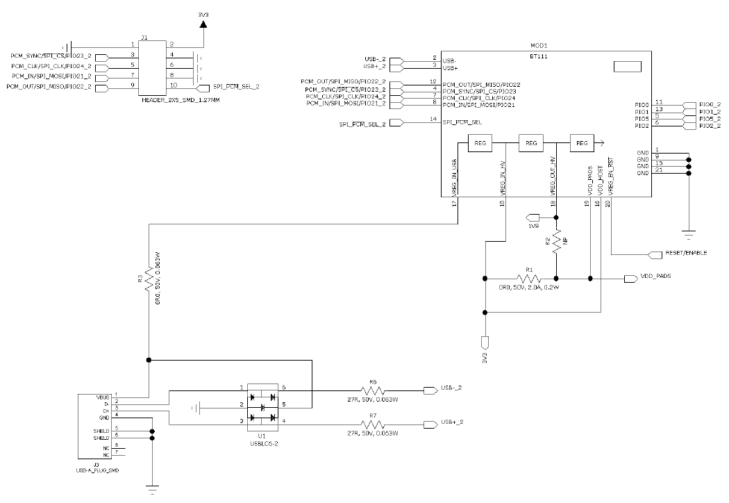
16 Example Schematic ................................................................................................................................ 43
17 Software .................................................................................................................................................. 44
17.1 On-chip Software ................................................................................................................................ 45
17.1.1 Bluetooth HCI Stack ...................................................................................................................... 45
17.1.2 Latest Feature of the HCI Stack .................................................................................................... 45
18 Soldering Recommendations .................................................................................................................. 46
19 Certifications ........................................................................................................................................... 47
19.1 Bluetooth ............................................................................................................................................ 47
19.2 FCC/IC (USA/Canada) ....................................................................................................................... 47
19.2.1 FCC et IC ...................................................................................................................................... 48
19.3 CE (Europe) ....................................................................................................................................... 49
19.4 Japan .................................................................................................................................................. 50
20 Moisture Sensitivity Level (MSL) classification ....................................................................................... 51
21 Packaging and Reel Information ............................................................................................................. 52
22 Contact Information................................................................................................................................. 54
Bluegiga Technologies Oy
BT111: Bluetooth Smart Ready HCI Module
DESCRIPTION
BT111 is a low cost and ultra-
small Bluetooth Smart Ready HCI module that
is designed for applications where
both Bluetooth classic and Bluetooth low
energy connectivity is needed. BT111
integrates a Bluetooth 4.0 dual mode radio,
HCI software stack, USB interface and an
antenna. BT111 is compatible with Windows
and Linux operating systems and Microsoft
and BlueZ Bluetooth stacks and offers OEMs
fast and risk free way to
integrate Bluetooth 4.0 connectivity into their
applications.
APPLICATIONS
Health and fitness gateways
Point of sale
M2M connectivity
Automotive aftermarket
Personal navigation devices
Consumer electronics
Industrial and home automation
gateways
KEY FEATURES
Bluetooth v.4.0, dual mode compliant
Support Bluetooth classic
Supports Bluetooth low
energy master and slave mode
Radio capabilities
Transmit power: +8dBm
Receiver sensitivity: -89dBm
Line-of-sight range: 100+ meters
Integrated antenna
Interfaces
HCI over USB host interface
802.11 co-existence interface
Software programmable GPIO
PCM or I2S audio interfaces
Supply voltage: 1.7V to 3.6V or 3.1V to
3.6V
Temperature range: -30C to +85C
Ultra compact size: 13.05mm x 9.30mm
Bluetooth, CE, FCC, IC and Japan
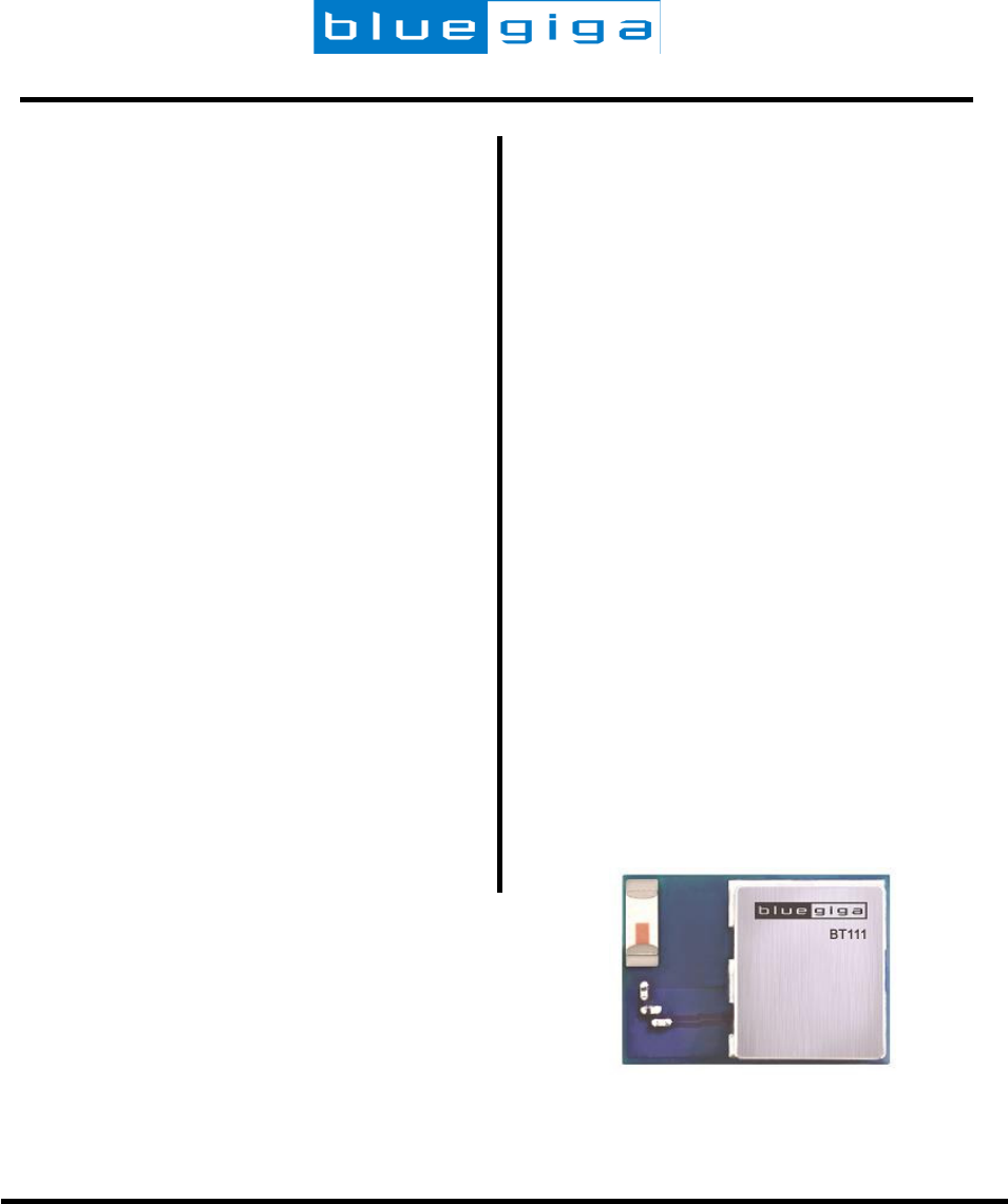
PHYSICAL OUTLOOK

Bluegiga Technologies Oy
Page 7 of 54
1 BT111 Product numbering
BT111-A-HCI
Firmware revision
Antenna:
A = Internal
Available products and product codes
Product code
Description
BT111-A-HCI
BT111 Bluetooth 4.0 HCI module with integrated antenna
Bluegiga Technologies Oy
Page 8 of 54
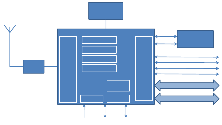
2 Block Diagram
64k EEPROM
PIO3
PIO4
26MHz XTAL
BPF
Antenna
PIO0
PIO1
PIO2
PIO5
SPI / PCM
USB
CSR8510
RF
RAM
ROM
MMU
MCU I/O
LDO 3V3 LDO 1V8
3 x LDO
1V3
5V0 3V3 1V8
Figure 1: Block diagram of BT111
CSR8510
BT111 is based on CSR8510 dual mode chip. The chip includes all the functions required for a complete
Bluetooth radio with on chip LDO regulators. The chip provides SPI, PCM and USB interfaces. Up to 4 general
purpose I/Os are available for general usage, such as Wi-Fi coexistence or general indicators.
Antenna
Antenna is a ceramic monopole chip antenna. See the antenna characteristics in chapter 7.
Band Pass Filter
The band pass filter filters the out of band emissions from the transmitter to meet the specific regulations for
type approvals of various countries.
64k EEPROM
The embedded 64k EEPROM can be used to store customizable parameters, such as maximum TX power,
PCM configuration, USB product ID, USB vendor ID and USB product description.
26MHz Crystal
The embedded 26MHz crystal is used for generating the internal digital clocks.
Bluegiga Technologies Oy
Page 9 of 54
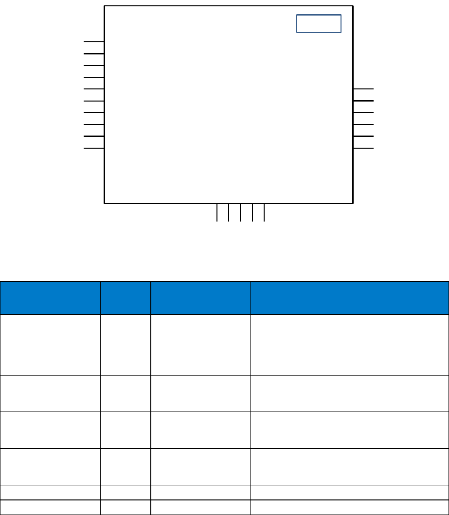
3 Pinout and Terminal Descriptions
1
2
3
4
5
6
7
8
9
10
GND
USB-
USB+
PCM_SYNC/SPI_CS/PIO23
PIO5
PIO2
PCM_CLK/SPI_CLK/PIO24
PCM_IN/SPI_MOSI/PIO21
GND
VREG_IN_HV
11
12
13
14
15
PIO0
PCM_OUT/SPI_MISO/PIO22
PIO01
SPI_PCM_SEL
GND
21
20
19
18
17
16VDD_HOST
VREG_IN_USB
VREG_OUT_HV
VDD_PADS
VREG_EN_RST#
GND
Figure 2: BT111
Power Supply
Pin No.
Pad Type
Description
VREG_EN_RST#
20
Input with strong
internal pull-down
Take high to enable internal regulators. Also
acts as active low reset. Maximum voltage is
VDD_PADS
Note: USB regulator is always enabled and
not controlled by this pin
VREG_IN_HV
10
Analogue regulator
input / output
Input to internal high-voltage regulator to
1.8V regulator, 3.3V output from USB
regulator.
VREG_OUT_HV
18
Analogue regulator
output
Output from internal high-voltage to 1.8V
regulator. Input to second stage internal
regulators.
VREG_IN_USB
17
Analogue regulator
input
Input to USB regulator. Connect to external
USB bus supply, e.g. USB_VBUS
VDD_HOST
16
VDD
USB system positive supply
VDD_PADS
19
VDD
Positive supply for digital I/O pads
Table 1: Supply Terminal Descriptions

Bluegiga Technologies Oy
Page 10 of 54
PIO Port
Pin No.
Pad Type
Supply Domain
Description
PIO0
11
Bidirectional, tristate,
with weak internal pull-
down
VDD_PADS
Programmable input/output line
PIO1
13
PIO2
6
PIO5
5
Table 2: I/O Terminal Descriptions
PCM Interface
Pin No.
Pad Type
Supply
Domain
Description
PCM_OUT/
SPI_MISO/
PIO22
12
Output, tristate, with
weak internal pull-
down
VDD_PADS
PCM syncronous data output
SPI data output
Programmable input/output line
PCM_IN/
SPI_MOSI/
PIO21
8
Input, tristate, with weak internal
pull-down
PCM syncronous data input
SPI data input
Programmable input/output line
PCM_SYNC/
SPI_CS#/
PIO23
4
Bidirectional, tristate, with weak
internal pulldown
PCM syncronous dara sync
SPI chip select, active low
Programmable input/output line
PCM_CLK/
SPI_CLK/
PIO24
7
PCM syncronous data clock
SPI clock
Programmable input/output line
SPI_PCM#_SEL
14
Input with weak internal pull-down
High switches SPI/PCM lines to SPI, low
switches SPI/PCM lines to PCM/PIO use
Table 3: PCM Interface
USB Interface
Pin No.
Pad Type
Supply
Domain
Description
USB+
3
Bidirectional
VDD_HOST
USB data plus with selectable internal 1.5kΩ
pull-up resistor
USB-
2
USB data minus
Table 4: USB Interface
Bluegiga Technologies Oy
Page 11 of 54
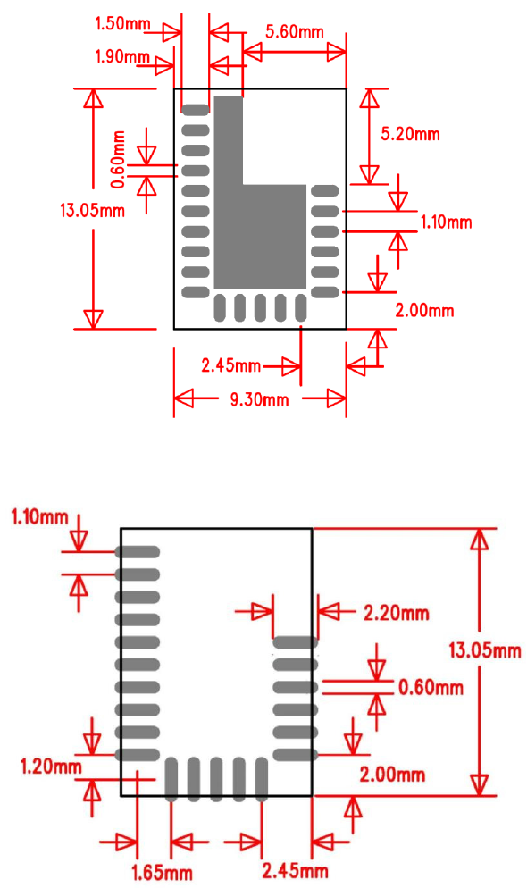
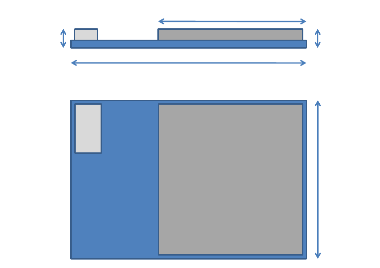
4 External Dimensions and Land Pattern
Figure 3: Footprint (top view)
Figure 4: Recommended PCB land pattern
Bluegiga Technologies Oy
Page 12 of 54
2.1mm (+/- 10%)
13.05mm (+/- 0.1mm)
1.9mm (+/- 10%)
7.3mm (+/- 0.1mm)
9.3mm (+/- 0.1mm)
Figure 5: External dimensions
Bluegiga Technologies Oy
Page 13 of 54
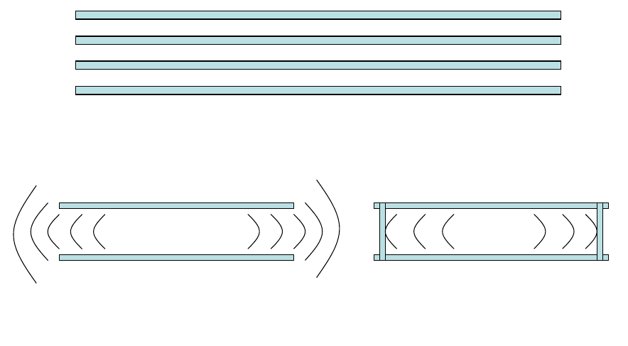
5 Layout Guidelines
Use good layout practices to avoid excessive noise coupling to supply voltage traces or sensitive analog
signal traces. If using overlapping ground planes use stitching vias separated by max 3 mm to avoid emission
from the edges of the PCB. Connect all the GND pins directly to a solid GND plane and make sure that there
is a low impedance path for the return current following the signal and supply traces all the way from start to
the end.
A good practice is to dedicate one of the inner layers to a solid GND plane and one of the inner layers to
supply voltage planes and traces and route all the signals on top and bottom layers of the PCB. This
arrangement will make sure that any return current follows the forward current as close as possible and any
loops are minimized.
•
–
–
–
•
–
–
–
–
Signals
GND
Power
Signals
Figure 6: Typical 4-layer PCB construction
Overlapping GND layers without
GND stitching vias
Overlapping GND layers with
GND stitching vias shielding the
RF energy
Figure 7: Use of stitching vias to avoid emissions from the edges of the PCB
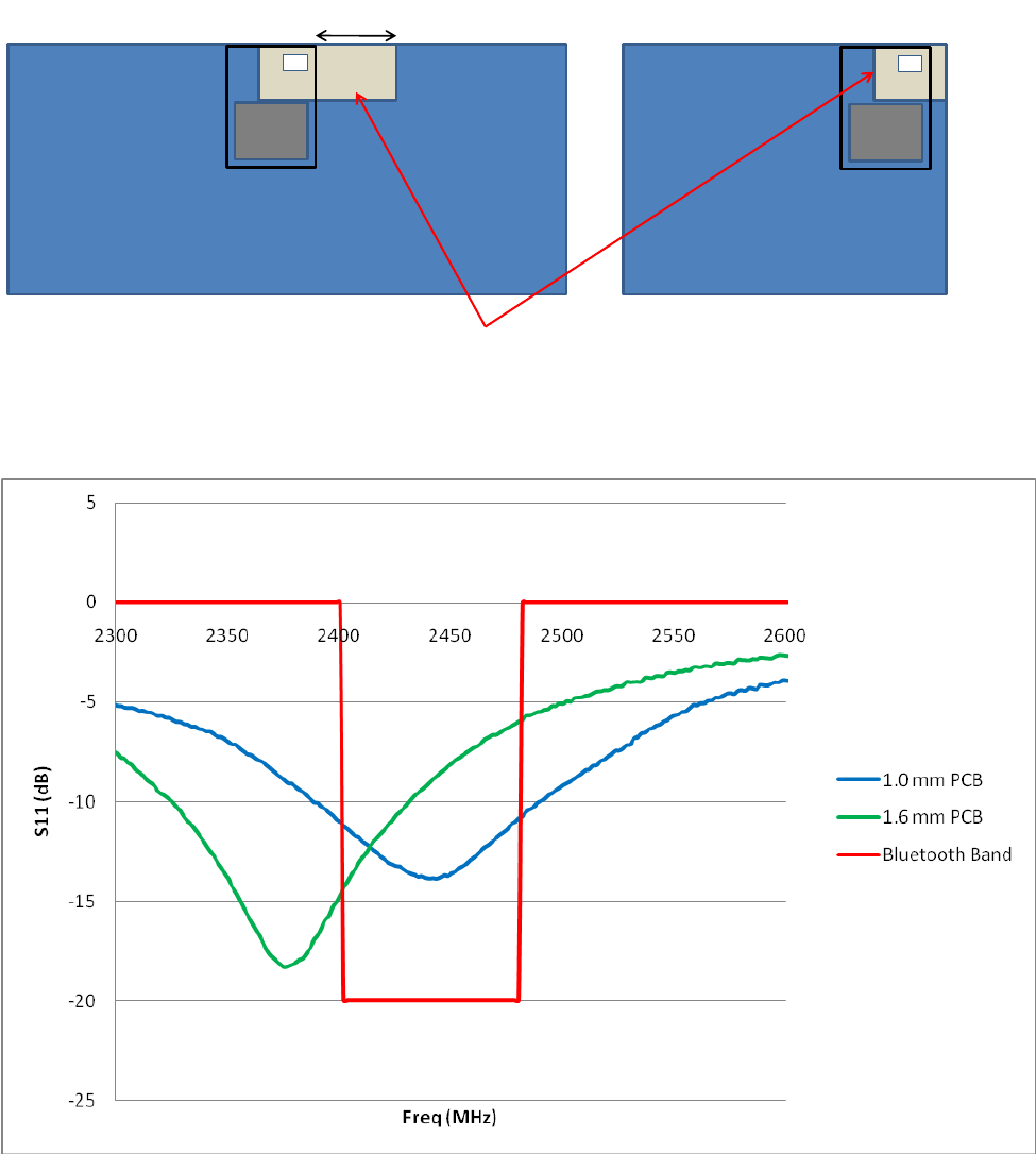
5.1 BT111-A Layout Guide
For optimal performance of the antenna place the module at the corner of the PCB of the mother board as
shown in the Figure 8. Optionally the module can be placed on the long edge of the mother board. In this case
the metal clearance area must be extended minimum 10mm from the edge of the module, as shown in Figure
8. The layout of the mother board has an impact on the antenna characteristic and radiation pattern, see the
antenna characteristics chapter. Do not place any metal (traces, components, battery etc.) within the
clearance area of the antenna. Connect all the GND pins directly to a solid GND plane. Place the GND vias as
close to the GND pins as possible. Use good layout practices to avoid any excessive noise coupling to signal
lines or supply voltage lines. Avoid placing plastic or any other dielectric material closer than 5 mm from the
antenna. Any dielectric closer than 5 mm from the antenna will detune the antenna to lower frequencies.
The antenna is optimized for mother board thickness of 1.0 mm. If the mother board is thicker than this, the
resonant frequency will be tuned downwards. If the mother board thickness is thinner than 1.0 mm, the
resonant frequency will be tuned upwards. S11 is a measure of how big portion of the transmitted power is
reflected back from the antenna. An adequate performance can be expected if S11 is less than – 7 dB. If
Bluegiga Technologies Oy
Page 14 of 54
using PCB thickness more than 1.6 mm, or if there is dielectric material around the antenna which is likely to
detune the resonant frequency, the antenna can be tuned in the mother board layout by removing FR4 below
the antenna.
Mother board
BT111
Mother board
BT111
Metal clearance area
Min. 10mm
Figure 8: Recommended layouts for BT111-A
Figure 9: Impedance matching of the antenna of BT111 with two different mother board PCB thickness
Bluegiga Technologies Oy
Page 15 of 54
6 Electrical Characteristics
6.1 Absolute Maximum Ratings
Rating
Min
Max
Unit
Storage temperature
-40
+85
⁰C
VREG_IN_USB
-0.2
5.85
V
VREG_IN_HV
-0.2
4.9
V
VDD_HOST
-0.2
3.7
V
VDD_PADS
-0.2
3.7
V
Other terminal voltages
VSS - 0.4V
VDD + 0.4 V
V
Table 5: Absolute maximum ratings
Rating
Min
Max
Unit
Operating temperature
-30
+85
⁰C
VREG_IN_USB
4.25
5.75
V
VREG_IN_HV
2.3
4.8
V
VDD_HOST
3.1
3.6
V
VDD_PADS (*
1.7(*
3.6(*
V
*) NOTE: The internal EEPROM is powered from VDD_PADS. To write the EEPROM,
minimum supply voltage is 2.7V and maximum is 3.3V. For reading the EEPROM the
minimum supply voltage is 1.7V and the maximum is 3.6V.
Table 6: Recommended operating conditions
6.2 Input/Output Terminal Characteristics
6.2.1 USB Linear Regulator
Rating
Min
Typ
Max
Unit
Input voltage
4.25
5.0
5.75
V
Output voltage
3.2
3.3
3.4
V
Output current
-
-
150
mA
Table 7: USB linear regulator

Bluegiga Technologies Oy
Page 16 of 54
6.2.2 High-voltage Linear Regulator
Normal Operation
Min
Typ
Max
Unit
Input voltage
2.3
3.3
4.8
V
Output voltage
1.75
1.85
1.95
V
Temperature coefficient
-200
-
200
pp/⁰C
Output noise (frequency range 100Hz to
100kHz)
-
-
0.4
mV rms
Settling time (settling ti within 10% of final
value)
-
-
5
µs
Output current
-
-
100
mA
Quiescent current (excluding load, Iload <1mA)
30
40
60
µA
Low-power Mode
Quiescent current (excluding load, Iload
<100µA)
14
18
23
µA
Table 8: High-voltage Linear Regulator
6.2.3 Digital
Normal Operation
Min
Typ
Max
Unit
Input Voltage
VIL input logic level low
-0.4
-
0.4
V
VIH input logic level high
0.7 x VDD
-
VDD + 0.4
V
Output Voltage
VOL output logic level low, IOL = 4.0mA
-
-
0.4
V
VOH output logic level high, IOL = 4.0mA
0.75 x VDD
-
-
V
Input and Tristate Currents
Strong pull-up
-150
-40
-10
µA
Striong pull-down
10
40
150
µA
Weak pull-up
-5
-1.0
-0.33
µA
Weak pull-down
0.33
1.0
5.0
µA
CI input capacitance
1.0
-
5.0
pF
Table 9: Digital I/O characteristics
Bluegiga Technologies Oy
Page 17 of 54
6.3 Current Consumption
Normal Operation
Peak
(8 dBm)
AVG
Unit
Idle
5
mA
USB Suspend
200
µA
Inguiry
73
51
mA
File Transfer
73
58
mA
LE Connected (Master)
74
(*
mA
LE Scan (Master)
48
(*
mA
*) LE AVG current consumption depends on the chosen TX interval and scanning window
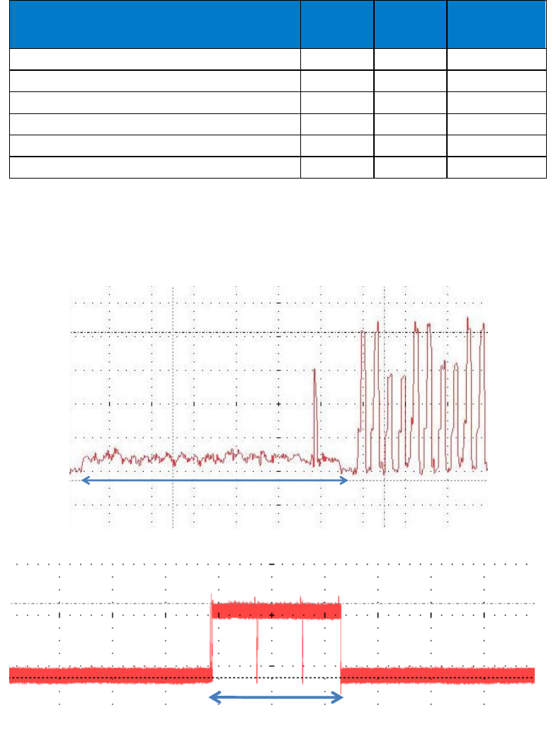
Table 10: Current consumption of BT111 with 8 dBm TX power
6.5 ms
TX Peak = 73 mA
Peak = 14 mA
Figure 10: Current consumption profile while creating a SPP connection
Peak = 48 mA
BGND Current = 6.4 mA
Window = 50 ms
Figure 11: LE scanning with 50 ms window
Bluegiga Technologies Oy
Page 18 of 54
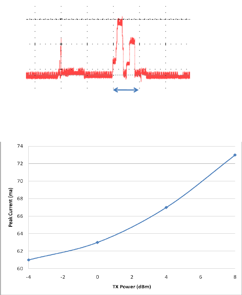
Peak = 74 mA
500 µs
AVG = 7.7 mA
(with 70 ms interval)
Figure 12: LE connected with 70 ms interval
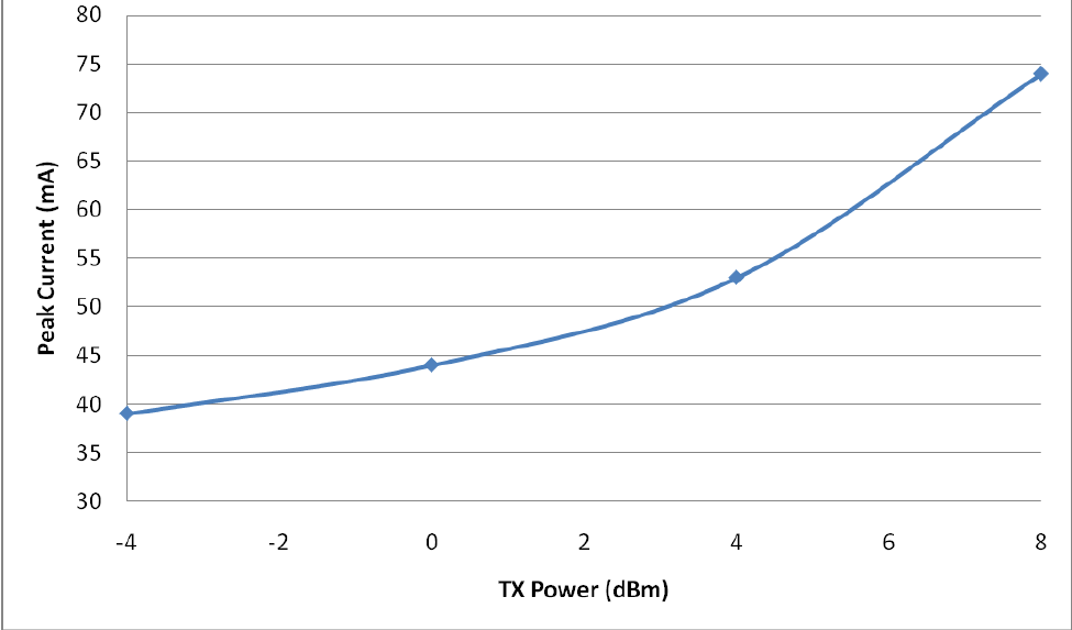
Figure 13: BDR Peak current vs TX power
Bluegiga Technologies Oy
Page 19 of 54
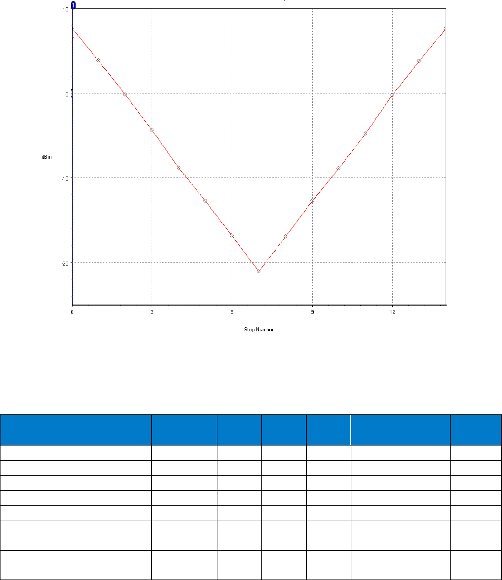
Figure 14: LE peak current vs. TX power

Bluegiga Technologies Oy
Page 20 of 54
7 RF Characteristics
7.1 Transmitter Characteristics
RF Characetristics, VDD = 3.3V @ room
temperature unless otherwise specified
Min
Typ
Max
Bluetooth
Specification
Unit
maximum RF Transmit Power
8
10
20
dBm
RF power variation over temperature range
1.5
-
dB
RF power variation over supply voltage range
0.2
-
dB
RF power variation over BT band (*
2
-
dB
RF power control range
-21
8
-
dBm
20dB band width for modulated carrier
1000
kHz
ACP (1
F = F0 ± 2MHz
-20
F = F0 ± 3MHz
-40
F = F0 > 3MHz
-40
Drift rate
10
+/-25
kHz
ΔF1avg
165
140<175
kHz
ΔF1max
168
140<175
kHz
ΔF2avg / ΔF1avg
0.9
>=0.8
*) Channel 0 @2402Mhz has generally 1.0 dB lower TX power than all the other channels. All the channels
between 2403 MHz and 2480 MHz are within 0.5 dB.
Table 11: Transmitter Characteristics, BDR
Bluegiga Technologies Oy
Page 21 of 54
Figure 15: Power control steps of BT111
7.2 Receiver Characteristics
RF characteristis, VDD = 3.3V,
room temperature
Packet type
Min
Typ
Max
Bluetooth
Spefication
Unit
Sensitivity for 0.1% BER
DH1
-89
-70
dBm
DH3
-89
dBm
DH5
-89
dBm
2-DH5
-92
dBm
3-DH5
-85
dBm
Sensitivity variation over BT band
(*
All
2
dB
Sensitivity variation over
temperature range
All
TBD
dB
*) Channel 0 @2402Mhz is generally 1.5dB less sensitive than all the other channels. All the channels
between 2403 MHz and 2480 MHz are within 0.5 dB.
Table 12: BDR and EDR receiver sensitivity

Bluegiga Technologies Oy
Page 22 of 54
7.3 Radiated Spurious Emissions
Standard
Band /
Frequency
Min
(AVG /
PEAK)
Typ
(AVG /
PEAK)
Max
(AVG /
PEAK)
Limit by the Standard
(AVG / PEAK)
Unit
FCC part 15
transmitter
spurious
emissions
2nd harmonic
51 / 58
54 / 74
dBuV/m
3rd harmonic
< 50
54 / 74
dBuV/m
Band edge
2483.5MHz
48 / -
54 / 74
dBuV/m
Band edge
2400MHz
-50
-20
dBc
Band edge
2483.5MHz
-35
-20
dBc
ETSI EN 300 328
transmitter
spurious
emissions
Band edge
2400MHz
-42
-30
dBm
2nd harmonic
-36
-30
dBm
3rd harmonic
<-40
-30
dBm
ETSI EN 300 328
receiver
spurious
emissions
(2400 - 2479)
MHz
<-70
-47
dBm
(1600 - 1653)
MHz
<-70
-47
dBm
Table 13: Radiated Spurious Emissions
7.4 Antenna Characteristics
The antenna is a standard monopole chip antenna. The radiation pattern is strongly dependent on the layout
of the mother board. Usually the gain is highest to the directions where there is most GND and weakest to the
opposite direction. Typically the total radiated efficiency is around 25% - 35%. The maximum gain is 0.5 dBi.
Bluegiga Technologies Oy
Page 23 of 54
8 Clock Generation
BT111 is using an internal 26 MHz crystal oscillator. All internal digital clocks are generated using a phase
locked loop, which is locked to the 26 MHz crystal oscillator. 26 MHz clock is calibrated in production and the
calibrated settings are stored to the internal EEPROM of BT111. The 32.768 kHz sleep clock is generated
internally to the module. BT111 does not need any external clock sources.

Bluegiga Technologies Oy
Page 24 of 54
9 Bluetooth Stack Microcontroller
BT111 uses a 16-bit RISC MCU for low power consumption and efficient use of memory.
The MCU, interrupt controller and event timer run the Bluetooth software stack and control the Bluetooth radio
and host interfaces.
10 Programmable I/O Ports
See the Device Terminal Functions section for the list of supplies to the PIOs.
PIO lines are configured through software to have either weak or strong pull-ups or pull-downs. All PIO lines
are configured as inputs with weak pull-downs at reset and have additional individual bus keeper
configuration. The default configuration for all the IO pins is input with weak pull-up.
11 Wi-Fi Coexistence Interface
Dedicated hardware is provided to implement a variety of Wi-Fi coexistence schemes. There is support for:
Channel skipping AFH
Priority signaling
Channel signaling
Host passing of channel instructions
The BT111 supports the Wi-Fi coexistence schemes:
Unity-3
Unity-3e
Unity+
Contact support (support@bluegiga.com) for more information
Bluegiga Technologies Oy
Page 25 of 54
12 Memory Management
12.1 Memory Management Unit
The MMU provides a number of dynamically allocated ring buffers that hold the data that is in transit between
the host and the air. The dynamic allocation of memory ensures efficient use of the available RAM and is
performed by a hardware MMU to minimize the overheads on the processor during data/voice transfers.
12.2 System RAM
56KB of integrated RAM supports the RISC MCU and is shared between the ring buffers for holding
voice/data for each active connection and the general-purpose memory required by the Bluetooth stack.
12.3 Internal ROM Memory (5Mb)
5Mb of internal ROM memory is available on BT111. This memory is provided for system firmware, storing
BT111 settings and program code.
12.4 Internal EEPROM
64kb internal EEPROM is available on BT111 to store device specific configuration information (PS Keys)
such as Bluetooth address, USB descriptors, PCM configuration and maximum TX power. The internal
EEPROM is powered from VDD_PADS. The minimum supply voltage writing the EEPROM is 2.7V and the
minimum supply voltage for reading the EEPROM is 1.7V.
Bluegiga Technologies Oy
Page 26 of 54
13 Serial Interfaces
13.1 USB Interface
BT111 has a full-speed (12Mbps) USB interface for communicating with other compatible digital devices. The
USB interface on BT111 acts as a USB peripheral, responding to requests from a master host controller.
BT111 supports the Universal Serial Bus Specification, Revision v2.0 (USB v2.0 Specification) and USB
Battery Charging Specification, available from http://www.usb.org. For more information on how to integrate
the USB interface on BT111 see the WT USB Design Guide available in Bluegiga Techforum.
As well as describing USB basics and architecture, the application note describes:
Power distribution for high and low bus-powered configurations
Power distribution for self-powered configuration, which includes USB VBUS monitoring
USB enumeration
Electrical design guidelines for the power supply and data lines, as well as PCB tracks and the effects
of ferrite beads
USB suspend modes and Bluetooth low-power modes:
Global suspend
Selective suspend, includes remote wake
Wake on Bluetooth, includes permitted devices and set-up prior to selective suspend
Suspend mode current draw
PIO status in suspend mode
Resume, detach and wake PIOs
Battery charging from USB, which describes dead battery provision, charge currents, charging in
suspend
Modes and USB VBUS voltage consideration
USB termination when interface is not in use
Internal modules, certification and non-specification compliant operation
See chapter 17 for the default USB vendor and product ID settings.
13.2 Programming and Debug Interface
This SPI programming and debug interface can configure the PS Keys stored in the internal EEPROM and
can also debug BT111. Bluegiga provides the development and production tools to communicate over this
interface from a PC.
BT111 uses a 16-bit data and 16-bit address programming and debug interface. Transactions occur when the
internal processor is running or is stopped. Data is written or read one word at a time, or the auto-increment
feature is available for the block access.
Configuring the parameters of the BT111 and running test scripts is also possible via the USB interface with
certain limitations; please see Section 14 for more information.
Bluegiga Technologies Oy
Page 27 of 54
14 Audio Interfaces
BT111 has digital audio interface that is configurable as either a PCM or I2S port.
14.1 PCM Interface
The audio PCM interface on the BT111 supports:
Continuous transmission and reception of PCM encoded audio data over Bluetooth.
Processor overhead reduction through hardware support for continual transmission and reception of
PCM data.
A bidirectional digital audio interface that routes directly into the baseband layer of the firmware. It
does not pass through the HCI protocol layer.
Hardware on BT111 for sending data to and from a SCO connection.
Up to 3 SCO connections on the PCM interface at any one time.
PCM interface master, generating PCM_SYNC and PCM_CLK.
PCM interface slave, accepting externally generated PCM_SYNC and PCM_CLK.
Various clock formats including:
o Long Frame Sync
o Short Frame Sync
o GCI timing environments
13-bit or 16-bit linear, 8-bit μ-law or A-law companded sample formats.
Receives and transmits on any selection of 3 of the first 4 slots following PCM_SYNC.
The PCM configuration options are enabled by setting PSKEY_PCM_CONFIG32.
14.1.1 PCM Interface Master/Slave
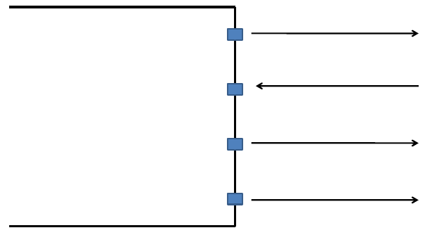
When configured as the master of the PCM interface, BT111 generates PCM_CLK and PCM_SYNC.
PCM_OUT
PCM_IN
PCM_CLK
PCM_SYNC
128/256/512/1536/2400kHz
8/48kHz
Figure 16: BT111 as PCM master
Bluegiga Technologies Oy
Page 28 of 54
PCM_OUT
PCM_IN
PCM_CLK
PCM_SYNC
Up to 2400kHz
8/48kHz
Figure 17: BT111 as PCM slave
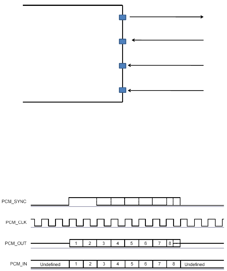
14.1.2 Long Frame Sync
Long Frame Sync is the name given to a clocking format that controls the transfer of PCM data words or
samples. In Long Frame Sync, the rising edge of PCM_SYNC indicates the start of the PCM word. When
BT111 is configured as PCM master, generating PCM_SYNC and PCM_CLK, then PCM_SYNC is 8 bits long.
When BT111 is configured as PCM Slave, PCM_SYNC is from 1 cycle PCM_CLK to half the PCM_SYNC
rate.
Figure 18: Long Frame Sync (Shown with 8-bit Companded Sample)
BT111 samples PCM_IN on the falling edge of PCM_CLK and transmits PCM_OUT on the rising edge.
PCM_OUT is configurable as high impedance on the falling edge of PCM_CLK in the LSB position or on the
rising edge.
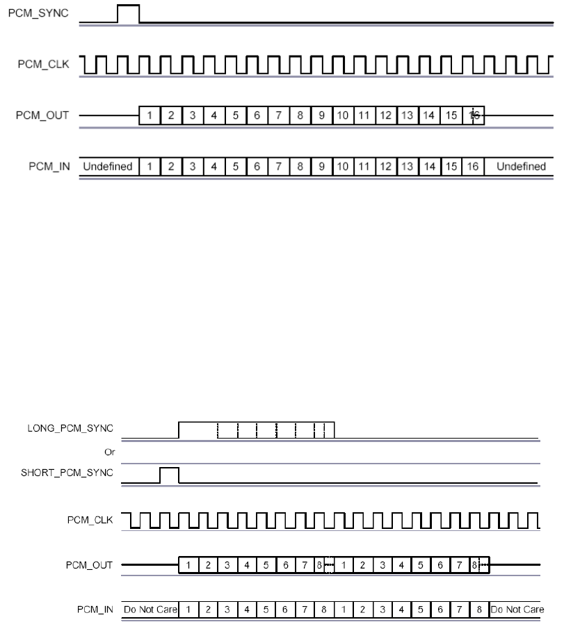
14.1.3 Short Frame Sync
In Short Frame Sync, the falling edge of PCM_SYNC indicates the start of the PCM word. PCM_SYNC is
always 1 clock cycle long.
Bluegiga Technologies Oy
Page 29 of 54
Figure 19: Short Frame Sync (shown with 16-bit sample)
As with Long Frame Sync, BT111 samples PCM_IN on the falling edge of PCM_CLK and transmits
PCM_OUT on the rising edge. PCM_OUT is configurable as high impedance on the falling edge of PCM_CLK
in the LSB position or on the rising edge.
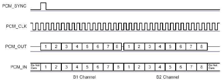
14.2 Multi-slot Operation
More than 1 SCO connection over the PCM interface is supported using multiple slots. Up to 3 SCO
connections are carried over any of the first 4 slots.
Figure 20: Multi-slot Operation with 2 Slots and 8-bit Companded Samples
14.2.1 GCI Interface
BT111 is compatible with the GCI, a standard synchronous 2B+D ISDN timing interface. The 2 64kbps B
channels are accessed when this mode is configured.
Bluegiga Technologies Oy
Page 30 of 54
Figure 21: GCI Interface
The start of frame is indicated by the rising edge of PCM_SYNC and runs at 8kHz.
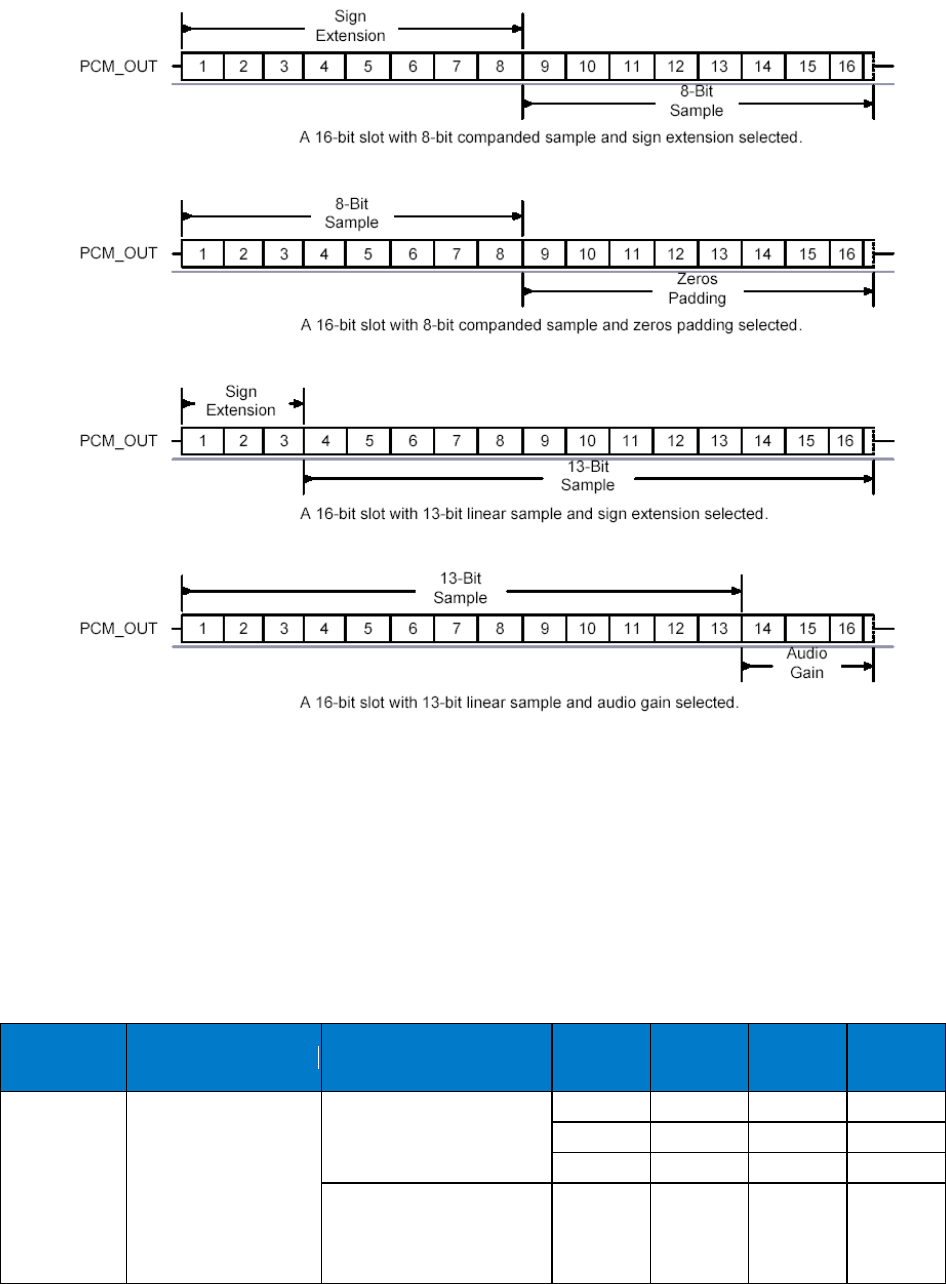
14.2.2 Slots and Sample Formats
BT111 receives and transmits on any selection of the first 4 slots following each sync pulse. Slot durations
are either 8 or 16 clock cycles:
8 clock cycles for 8-bit sample formats.
16 clock cycles for 8-bit, 13-bit or 16-bit sample formats.
BT111 supports:
13-bit linear, 16-bit linear and 8-bit μ-law or A-law sample formats.
A sample rate of 8ksps.
Little or big endian bit order.
For 16-bit slots, the 3 or 8 unused bits in each slot are filled with sign extension, padded with zeros or
a programmable 3-bit audio attenuation compatible with some codecs.
Bluegiga Technologies Oy
Page 31 of 54
Figure 22: 16-bit Slot Length and Sample Formats
14.2.3 Additional Features
BT111 has a mute facility that forces PCM_OUT to be 0. In master mode, BT111is compatible with some
codecs which control power down by forcing PCM_SYNC to 0 while keeping PCM_CLK running.
14.2.4 PCM Timing Information
Symbol
Parameter
Min
Typ
Max
Unit
fmclk
PCM_CLK
Frequency
4MHz DDS generation.
Ffrequency selection is
programmable.
-
128
-
kHz
256
512
48MHz DDS generation.
Frequency selection is
programmable.
2.9
-
-

Bluegiga Technologies Oy
Page 32 of 54
-
PCM_SYNC frequency for SCO connection
-
8
-
kHz
fmclkh
(a)
PCM_CLK high
4MHz DDS generation
980
-
-
ns
fmclkl
(a)
PCM_CLK low
4MHz DDS generation
730
-
-
ns
-
PCM_CLK jitter
48MHz DDS generation
-
-
21
ns pk-pk
Table 14: PCM Master Timing
(a) Assumes normal system clock operation. Figures vary during low-power modes, when system speeds
are reduced.
Symbol
Parameter
Min
Typ
Max
Unit
tdmclksynch
Delay time from
PCM_CLK high to
PCM sync high
4MHz DDS generation.
Ffrequency selection is
programmable.
-
-
20
ns
48MHz DDS generation
-
-
40.83
tdmclkpout
Delay time from PCM_CLK high to PCM_OUT
-
-
20
tdmclksyncl
Delay time from
PCM_CLK low to
PCM sync low (long
frame sync only)
4MHz DDS generation
-
-
20
48MHz DDS generation
-
-
40.83
tdmclklpoutz
Delay time from PCM_CLK low to PCM_OUT
high impedance
-
-
20
tdmclkhpoutz
Delay time from PCM_CLK high to PCM_OUT
high impedance
-
-
20
tsupinclkl
Set-up time for PCM_IN valid to PCM_CLK low
20
-
-
thpinclkl
Hold time for PCM_CLK low to PCM_IN invalid
0
-
-
Table 15: PCM Master Mode Timing Parameters
Bluegiga Technologies Oy
Page 33 of 54
Figure 23: PCM Master Timing Long Frame Sync
Figure 24: PCM Master Timing Short Frame Sync

Bluegiga Technologies Oy
Page 34 of 54
Symbol
Parameter
Min
Typ
Max
Unit
fsclk
PCM clock frequency
(Slave mode: Input)
64
-
2048
kHz
fsclk
PCM clock frequency
(GCI mode)
128
-
4096
kHz
fsclkl
PCM_CLK low time
200
-
-
ns
fsclkh
PCM_CLK high time
200
-
-
ns
Table 16: PCM Slave Timing
Symbol
Parameter
Min
Typ
Max
Unit
fhsclksynch
Hold time from PCM_CLK low to PCM_SYNC high
2
-
-
ns
fsusclksynch
Set-up time for PCM_SYNC high to PCM_CLK low
20
-
-
fdpout
Delay time from PCM_SYNC or PCM_CLK, whichever
is later, to valid PCM_OUT data (long frame sync only)
-
-
15
fdsclkhpout
Delay time from PCM_SYNC or PCM_CLK, whichever
is later, to valid PCM_OUT data
-
-
15
fdpoutz
Delay time from PCM_SYNC or PCM_CLK low,
whichever is later, to PCM_OUT data line high
impedance
-
-
20
fsupinsclkl
Set-up time for PCM_IN valid to PCM_CLK low
20
-
-
fhpinsclkl
Hold time from PCM_CLK low to PCM_IN valid
2
-
-
Table 17: PCM Slave Mode Timing Parameters
Bluegiga Technologies Oy
Page 35 of 54
Figure 25: PCM Slave Timing Long Frame Sync
Figure 26: PCM Slave Timing Short Frame Sync
14.2.5 PCM_CLK and PCM_SYNC Generation
BT111 has 2 methods of generating PCM_CLK and PCM_SYNC in master mode:
Generating these signals by DDS from BT111 internal 4MHz clock. Using this mode limits PCM_CLK
to 128, 256 or 512kHz and PCM_SYNC to 8kHz.
Generating these signals by DDS from an internal 48MHz clock, enables a greater range of
frequencies to be generated with low jitter but consumes more power. To select this second method
set bit 48M_PCM_CLK_GEN_EN in PSKEY_PCM_CONFIG32. When in this mode and with long
Bluegiga Technologies Oy
Page 36 of 54
frame sync, the length of PCM_SYNC is either 8 or 16 cycles of PCM_CLK, determined by
LONG_LENGTH_SYNC_EN in PSKEY_PCM_CONFIG32.
Following equation describes PCM_CLK frequency when generated from the internal 48MHz clock:
Equation 1: PCM_CLK Frequency Generated Using the Internal 48MHz Clock
Set the frequency of PCM_SYNC relative to PCM_CLK using following equation:
Equation 2: PCM_SYNC Frequency Relative to PCM_CLK
CNT_RATE, CNT_LIMIT and SYNC_LIMIT are set using PSKEY_PCM_LOW_JITTER_CONFIG. As an
example, to generate PCM_CLK at 512kHz with PCM_SYNC at 8kHz, set
PSKEY_PCM_LOW_JITTER_CONFIG to 0x08080177.
14.2.6 PCM Configuration
Configure the PCM by using PSKEY_PCM_CONFIG32 and PSKEY_PCM_LOW_JITTER_CONFIG, see your
PS Key file. The default for PSKEY_PCM_CONFIG32 is 0x00800000, i.e. first slot following sync is active, 13-
bit linear voice format, long frame sync and interface master generating 256kHz PCM_CLK from 4MHz
internal clock with no tri-state of PCM_OUT.
14.3 Digital Audio Interface (I2S)
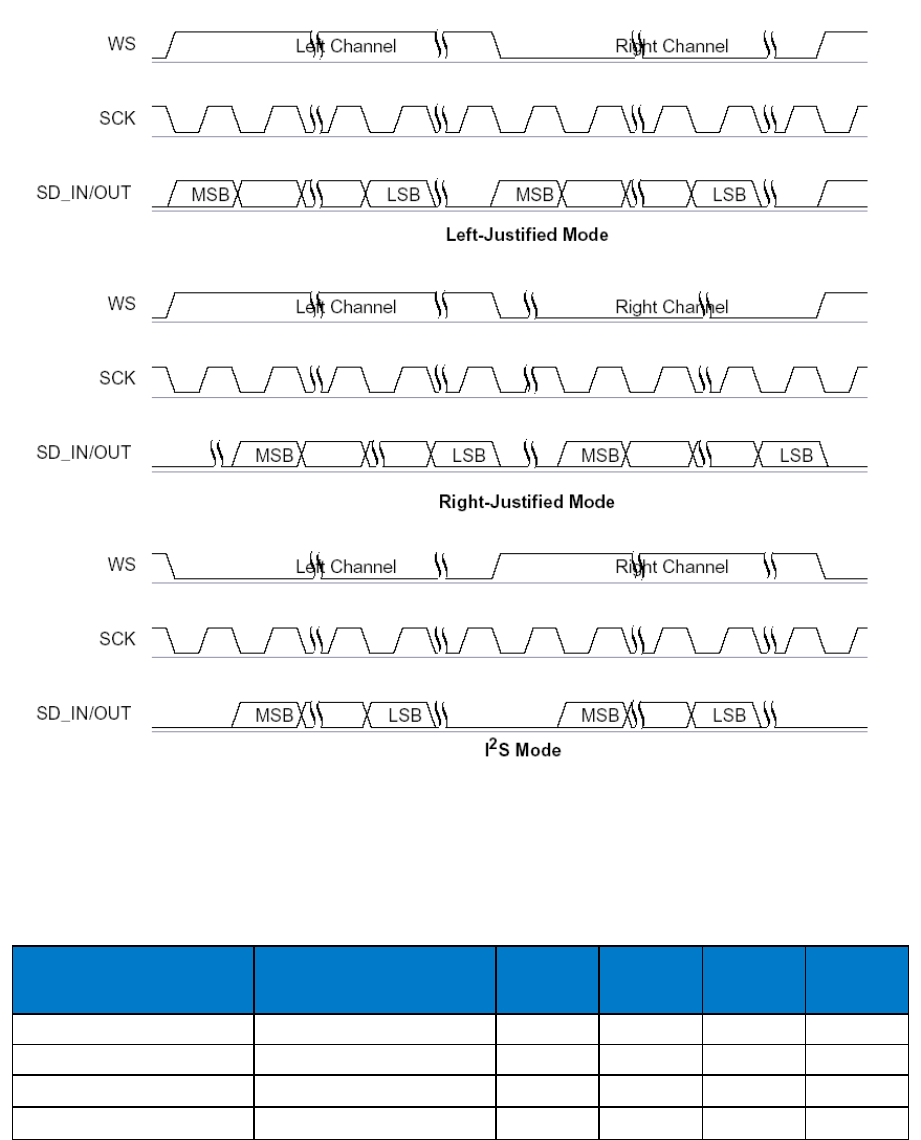
The digital audio interface supports the industry standard formats for I²S, left-justified or right-justified. The
interface shares the same pins as the PCM interface, which means each audio bus is mutually exclusive in its
usage. Table 17 lists these alternative functions.
PCM Interface
I2S Interface
PCM_OUT
SD_OUT
PCM_IN
SD_IN
PCM_SYNC
WS
PCM_CLK
SCK
Table 18: Alternative Function of the Digital Audio Bus Interface on the PCM Interface
Configure the digital audio interface using PSKEY_DIGITAL_AUDIO_CONFIG. Table 18 describes the values
for the PS Key (PSKEY_DIGITAL_AUDIO_CONFIG) that is used to set-up the digital audio interface. For
example, to configure an I2S interface with 16-bit SD data set PSKEY_DIGITAL_CONFIG to 0x0406.

Bluegiga Technologies Oy
Page 37 of 54
Bit
Mask
Name
Description
D[0]
0x0001
CONFIG_JUSTIFY_FORMAT
0 for left justified, 1 for right justified
D[1]
0x0002
CONFIG_LEFT_JUSTIFY_DELAY
For left justified formats: 0 is MSB of SD data
occurs in the first SCLK period following WS
transition. 1 is MSB of SD data occurs in the
second SCLK period.
D[2]
0x0004
CONFIG_CHANNEL_POLARITY
For 0, SD data is left channel when WS is high.
For 1 SD data is right channel.
D[3]
0x0008
CONFIG_AUDIO_ATTEN_EN
For 0, 17 bit SD data is rounded down to 16
bits. For 1, the audio attenuation defined in
CONFIG_AUDIO_ATTEN is applied over 24
bits with saturated rounding. Requires
CONFIG_16_BIT_CROP_EN to be 0.
D[7:4]
0x00F0
CONFIG_AUDIO_ATTEN
Attenuation in 6 dB steps.
D[9:8]
0x0300
CONFIG_JUSTIFY_RESOLUTION
Resolution of data on SD_IN, 00=16 bit, 01=20
bit, 10=24 bit, 11=Reserved. This is required for
right justified format and with left justified LSB
first.
D[10]
0x0400
CONFIG_16_BIT_CROP_EN
For 0, 17 bit SD_IN data is rounded down to 16
bits. For 1 only the most significant 16 bits of
data are received.
Table 19: PSKEY_DIGITAL_AUDIO_CONFIG
Bluegiga Technologies Oy
Page 38 of 54
Figure 27: Digital Audio Interface Modes
The internal representation of audio samples within BT111 is 16-bit and data on SD_OUT is limited to 16-bit
per channel.
Symbol
Parameter
Min
Typ
Max
Unit
-
SCK Frequency
-
-
6.2
MHz
-
WS Frequency
-
-
96
kHz
tch
SCK high time
80
-
-
ns
tcl
SCK low time
80
-
-
ns
Table 20: Digital Audio Interface Slave Timing
Bluegiga Technologies Oy
Page 39 of 54
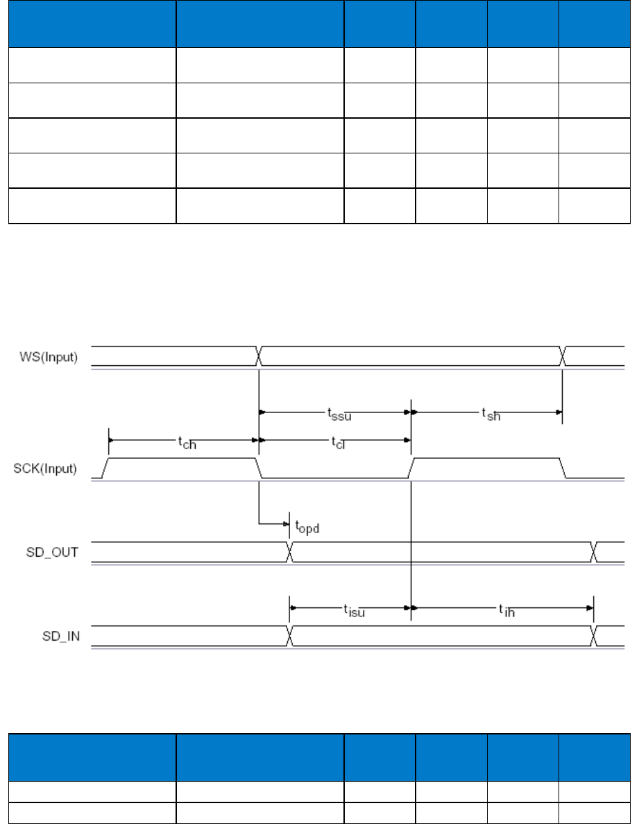
Symbol
Parameter
Min
Typ
Max
Unit
tssu
WS valid SCK high set-up
time
20
-
-
ns
tsh
SCK high to WS invalid
hold time
2.5
-
-
ns
topd
SCK low to SD_OUT valid
delay time
-
-
20
ns
tisu
SD_IN valid to SCK high
set-up time
20
-
-
ns
tih
SCK high to SD_IN invalid
hold time
2.5
-
-
ns
Table 21: I2C Slave Mode Timing
Figure 28: Digital Audio Interface Slave Timing
Symbol
Parameter
Min
Typ
Max
Unit
-
SCK Frequency
-
-
6.2
MHz
-
WS Frequency
-
-
96
kHz
Table 22: Digital Audio Interface Master Timing
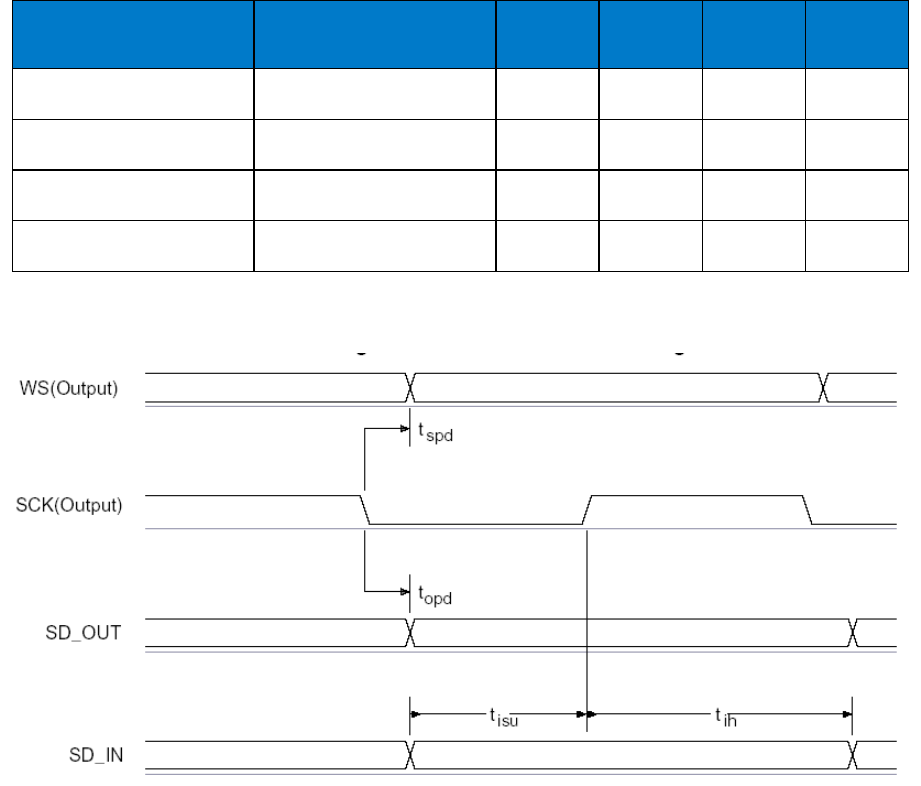
Bluegiga Technologies Oy
Page 40 of 54
Symbol
Parameter
Min
Typ
Max
Unit
tspd
SCK low to WS valid
delay time
-
-
39.27
ns
topd
SCK low to SD_OUT valid
delay time
-
-
18.44
ns
tisu
SD_IN valid to SCK high
set-up time
18.44
-
-
ns
tih
SCK high to SD_IN invalid
hold time
0
-
-
ns
Table 23: I2S Master Mode Timing Parameters, WS and SCK as Outputs
Figure 29: Digital Audio Interface Master Timing
Bluegiga Technologies Oy
Page 41 of 54
15 Power Control and Regulation
LDO 3V3 LDO 1V8 LDO 1V35
VBUS (4.25V –5.75V)
VREG_IN_HV
(3.3V OUT / 2.3V –4.8V IN)
VREG_OUT_HV
1.8V OUT / 1.7V –1.95V IN
VREG_EN_RST#
LDO 1V35
LDO 1V25
Figure 30: Internal regulators and powering of BT111
15.1 Voltage Regulator Enable
All the regulators are enabled, except the USB linear regulator, by taking the VREG_EN_RST# pin above 1V.
Also the BT111 firmware automatically controls the regulators.
Important Note:
VREG_EN_RST# should not be taken high before the supply on VREG_IN_HV is present.
The VREG_EN_RST# pin is connected internally to the reset function and is powered from VDD_PADS, so do
not apply voltages above VDD_PADS to the VREG_EN_RST# pin. The VREG_EN_RST# pin is pulled down
internally.
15.2 USB Linear Regulator
The integrated USB LDO linear regulator is available as a 3.30V supply rail and is intended to supply the USB
interface and the high-voltage linear regulator. The input voltage range is between 4.25V and 5.75V. The
maximum current from this regulator is 150mA.
This regulator is enabled by default. If the USB linear regulator is not required leave its input (VREG_IN_USB)
unconnected.
15.3 High Voltage Linear Regulator
The integrated high-voltage linear regulator is available to power the main 1.8V supply rail. The input voltage
range is between 2.3V and 4.8V. The maximum current from this regulator is 100mA.
Take VREG_EN_RST# high to enable this regulator.
Important Note:
VREG_EN_RST# should not be taken high before the supply on VREG_IN_HV is present.
If this regulator is not required then leave VREG_IN_HV unconnected or tied to VREG_OUT_HV.

Bluegiga Technologies Oy
Page 42 of 54
15.4 Low Voltage Linear Regulators
BT111 has three integrated low voltage linear regulators providing the internal supply voltages for RF and
digital circuits of BT111. The input voltage range is between 1.70V and 1.95V.
15.5 Powering Sequence
All the power supplies should be powered at the same time. The order of powering the supplies relative to the
I/O supply, VDD_PADS to VDD_HOST, is not important. If the I/O supply is powered before VDD_DIG, all
digital I/Os are weak pull-downs irrespective of the reset state.
15.6 Reset
The reset function is internally tied to the VREG_EN_RST# pin. BT111 is reset from several sources:
VREG_EN_RST# pin
Power-on reset
Via a software-configured watchdog timer
The VREG_EN_RST# pin is an active low reset. Assert the reset signal for a period >5ms to ensure a full
reset.
Important Note:
Bluegiga does not recommend assertions of the reset of <5ms on the VREG_EN_RST# pin, as any glitches
on this line can affect I/O integrity without triggering a reset.
A warm reset function is also available under software control. After a warm reset the RAM data remains
available.
Pin Name/Group
I/O Type
No Core Supply Reset
Full Chip Reset
VREG_EN_RST#
Digital input
Strong pull-down
N/A
SPI_CLK/PCM_CLK /
PIO[24]
Digital bidirectional
tristated
Weak pull-down
Weak pull-down
SPI_CS# / PCM_SYNC /
PIO[23]
Digital bidirectional
tristated
Weak pull-up (SPI)
Weak pull-down (PCM)
Weak pull-up (SPI)
Weak pull-down (PCM
/ PIO)
SPI_MISO / PCM_OUT /
PIO[22]
Digital output tristated
Weak pull-down
Weak pull-down
SPI_MOSI / PCM_OUT /
PIO[21]
Digital input
Weak pull-down
Weak pull-down
PIO[5:0]
Digital bidirectional
tristated
Weak pull-down
Weak pull-down
Table 24: Digital Pin States on Reset
Bluegiga Technologies Oy
Page 43 of 54
16 Example Schematic
Figure 31: Example schematic for BT111

Bluegiga Technologies Oy
Page 44 of 54
17 Software
BT111 is supplied with an on-chip Bluetooth v4.0 specification qualified HCI Controller stack firmware. It also
has an EEPROM chip, which allows modifications of many configuration parameters (PS-keys) of the
Bluetooth chip.
When the BT111 development kit is plugged into your PC, it will show up as a generic Bluetooth Controller,
and the Bluetooth Host stack installed on your PC will take control of it.
To access BT111’s configuration parameters, which are stored on its EEPROM chip, you need the included
SPI connector and PSTool software from the CSR BlueSuite tool collection. BlueSuite is available on the
Bluegiga Techforum at http://techforum.bluegiga.com.
PSTool contains a full list of the parameters that are possible to modify, along with their descriptions. Some
common parameter keys are:
- (0x0108) PSKEY_DEVICE_NAME – Bluetooth name of the device
- (0x02be) PSKEY_USB_VENDOR_ID – USB Vendor ID, if you have your own VID and wish to use it
(Default is 0a12 which is CSR’s VID)
- (0x02bf) PSKEY_USB_PRODUCT_ID – USB Product ID (Default is 0)
Please see the quick start guide for more information and examples.
Bluegiga Technologies Oy
Page 45 of 54
17.1 On-chip Software
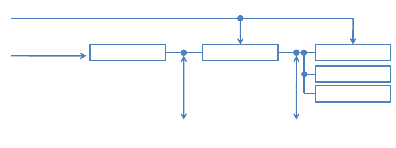
17.1.1 Bluetooth HCI Stack
Figure 32 shows an example implementation. An internal processor runs the Bluetooth stack up to the HCI.
The host processor must provide all the upper layers of Bluetooth protocol including the application.
Bluetooth HCI Handling ULP HIF Handling
LM ULP LL Control Handling
LC: Bluetooth per Packet Code LC: ULP per packet Code
LC: Bluetooth per Packet Code LC: ULP per Packet Code
Host Transport Device Drivers
Generic Command and Event Handling
Generic HCI Handling
LC Core Scheduler
2.4GHz Radio Hardware
PCM USB
Figure 32: Example FW Architecture
17.1.2 Latest Feature of the HCI Stack
BT111 is based on Bluetooth v4.0 qualified chip CSR8510 by CSR. This introduces the following features:
Generic Alternate MAC/PHY (AMP)
Generic Test Methodology for AMP
802.11 Protocol Adaptation Layer
Enhanced Power Control
Enhanced USB and SDIO HCI Transports
HCI read Encryption Key Size command
Unicast Connectionless Data
For Bluetooth v3.0 + HS operation a separate 802.11 IC is used in conjunction with BT111
Bluegiga Technologies Oy
Page 46 of 54
18 Soldering Recommendations
BT111 is compatible with a industrial standard reflow profile for Pb-free solders. The reflow profile used is
dependent on the thermal mass of the entire populated PCB, heat transfer efficiency of the oven and
particular type of solder paste used. Consult the datasheet of particular solder paste for profile configurations.
Bluegiga Technologies will give following recommendations for soldering the module to ensure the reliable
solder joint and operation of the module after soldering. Since the profile used is process and layout
dependent, the optimal profile should be studied case by case. Thus the following recommendation should be
taken into account as a starting point.
Refer to technical documentations of particular solder paste for profile configurations
Avoid using more than one flow.
Reliability of the solder joint and self-alignment of the component are dependent on the solder
volume. Minimum of 150m stencil thickness is recommended.
Aperture size of the stencil should be 1:1 with the pad size.
A low residue, “no clean” solder paste should be used due to low mounted height of the
component.

Bluegiga Technologies Oy
Page 47 of 54
19 Certifications
19.1 Bluetooth
BT111 is based on Bluetooth v4.0 qualified chip CSR8510 by CSR. BT111 can be used as a controller
subsystem with the Bluetooth QD ID B017701. To make a complete Bluetooth end product, Controller
Subsystem is used together with a qualified Host Subsystem.
19.2 FCC/IC (USA/Canada)
This device complies with Part 15 of the FCC Rules. Operation is subject to the following two conditions:
(1) this device may not cause harmful interference, and
(2) this device must accept any interference received, including interference that may
cause undesired operation.
Any changes or modifications not expressly approved by Bluegiga Technologies could void the
user’s authority to operate the equipment.
FCC RF Radiation Exposure Statement:
This equipment complies with FCC radiation exposure limits set forth for an uncontrolled environment. End
users must follow the specific operating instructions for satisfying RF exposure compliance. This transmitter
meets both portable and mobile limits as demonstrated in the RF Exposure Analysis and should not be used
closer than 5 mm from a human body in portable configuration. This transmitter must not be co-located or
operating in conjunction with any other antenna or transmitter except in accordance with FCC multi-transmitter
product procedures.
IC Statements:
This device complies with Industry Canada licence-exempt RSS standard(s). Operation is subject to the
following two conditions: (1) this device may not cause interference, and (2) this device must accept any
interference, including interference that may cause undesired operation of the device.
Under Industry Canada regulations, this radio transmitter may only operate using an antenna of a type and
maximum (or lesser) gain approved for the transmitter by Industry Canada. To reduce potential radio
interference to other users, the antenna type and its gain should be so chosen that the equivalent isotropically
radiated power (e.i.r.p.) is not more than that necessary for successful communication.
OEM Responsibilities to comply with FCC and Industry Canada Regulations
The BT111 module has been certified for integration into products only by OEM integrators under the following
condition:
The antenna(s) must be installed such that a minimum separation distance of 5 mm is maintained
between the radiator (antenna) and all persons at all times.
The transmitter module must not be co-located or operating in conjunction with any other antenna or
transmitter except in accordance with FCC multi-transmitter product procedures.

Bluegiga Technologies Oy
Page 48 of 54
As long as the two condition above is met, further transmitter testing will not be required. However, the OEM
integrator is still responsible for testing their end-product for any additional compliance requirements required
with this module installed (for example, digital device emissions, PC peripheral requirements, etc.).
IMPORTANT NOTE: In the event that these conditions can not be met (for certain configurations or co-
location with another transmitter), then the FCC and Industry Canada authorizations are no longer considered
valid and the FCC ID and IC Certification Number can not be used on the final product. In these
circumstances, the OEM integrator will be responsible for re-evaluating the end product (including the
transmitter) and obtaining a separate FCC and Industry Canada authorization.
End Product Labeling
The BT111 module is labeled with its own FCC ID and IC Certification Number. If the FCC ID and IC
Certification Number are not visible when the module is installed inside another device, then the outside of the
device into which the module is installed must also display a label referring to the enclosed module. In that
case, the final end product must be labeled in a visible area with the following:
“Contains Transmitter Module FCC ID: QOQBT111”
“Contains Transmitter Module IC: 5123A-BGTBT111”
or
“Contains FCC ID: QOQBT112”
“Contains IC: 5123A-BGTBT111”
The OEM integrator has to be aware not to provide information to the end user regarding how to install or
remove this RF module or change RF related parameters in the user manual of the end product.
19.2.1 FCC et IC
Déclaration d’IC :
Ce dispositif est conforme aux normes RSS exemptes de licence d’Industrie Canada. Son fonctionnement est
assujetti aux deux conditions suivantes : (1) ce dispositif ne doit pas provoquer de perturbation et (2) ce
dispositif doit accepter toute perturbation, y compris les perturbations qui peuvent entraîner un fonctionnement
non désiré du dispositif.
Selon les réglementations d’Industrie Canada, cet émetteur radio ne doit fonctionner qu’avec une antenne
d’une typologie spécifique et d’un gain maximum (ou inférieur) approuvé pour l’émetteur par Industrie
Canada. Pour réduire les éventuelles perturbations radioélectriques nuisibles à d’autres utilisateurs, le type
d’antenne et son gain doivent être choisis de manière à ce que la puissance isotrope rayonnée équivalente
(P.I.R.E.) n’excède pas les valeurs nécessaires pour obtenir une communication convenable.
Responsabilités des OEM quant à la conformité avec les réglementations de FCC et d’Industrie
Canada
Les modules BT111 ont été certifiés pour entrer dans la fabrication de produits exclusivement réalisés par des
intégrateurs dans les conditions suivantes :
Bluegiga Technologies Oy
Page 49 of 54
L’atee ou les atees doit te istalle de faço à aitei à tout istant une distance
minimum de 5 m ete la souce de adiatio l’atee et toute pesoe physiue.
Le module transmetteur ne doit pas être installé ou utilisé en concomitance avec une autre antenne
ou un autre transmetteur.
Tant que ces deux conditions sont réunies, il n’est pas nécessaire de procéder à des tests supplémentaires
sur le transmetteur. Cependant, l’intégrateur est responsable des tests effectués sur le produit final afin de se
mettre en conformité avec d’éventuelles exigences complémentaires lorsque le module est installé (exemple :
émissions provenant d’appareils numériques, exigences vis-à-vis de périphériques informatiques, etc.)
REMARQUE IMPORTANTE : En cas d’inobservance de ces conditions (en ce qui concerne certaines
configurations ou l’emplacement du dispositif à proximité d’un autre émetteur), les autorisations de FCC et
d’Industrie Canada ne seront plus considérées valables et l’identification de FCC et le numéro de certification
d’IC ne pourront pas être utilisés sur le produit final. Dans ces cas, l’intégrateur OEM sera chargé d’évaluer à
nouveau le produit final (y compris l’émetteur) et d’obtenir une autorisation indépendante de FCC et
d’Industrie Canada.
Étiquetage du produit final
Le module BT111 est étiqueté avec sa propre identification FCC et son propre numéro de certification IC. Si
l’identification FCC et le numéro de certification IC ne sont pas visibles lorsque le module est installé à
l’intérieur d’un autre dispositif, la partie externe du dispositif dans lequel le module est installé devra
également présenter une étiquette faisant référence au module inclus. Dans ce cas, le produit final devra être
étiqueté sur une zone visible avec les informations suivantes :
« Contient module émetteur identification FCC : QOQBT111 »
« Contient module émetteur IC : 5123A-BGTBT111 »
ou
« Contient identification FCC : QOQBT111 »
« Contient IC : 5123A-BGTBT111 »
Dans le guide d’utilisation du produit final, l’intégrateur OEM doit s’abstenir de fournir des informations à
l’utilisateur final portant sur les procédures à suivre pour installer ou retirer ce module RF ou pour changer les
paramètres RF.
19.3 CE (Europe)
BLE112 is in conformity with the essential requirements and other relevant requirements of the R&TTE
Directive (1999/5/EC). The product is conformity with the following standards and/or normative documents.
EMC (immunity only) EN 301 489-17 V2.1.1
Radiated emissions EN 300 328 V1.7.1
Safety EN60950-1:2006+A11:2009+A1:2010+A12:2011
Bluegiga Technologies Oy
Page 50 of 54
19.4 Japan
TBA
Bluegiga Technologies Oy
Page 51 of 54
20 Moisture Sensitivity Level (MSL) classification
Moisture sensitivity level (MSL) of this product is 3. Please follow the handling guidelines of the standard
IPC/JEDEC J-STD-020 and J-STD-033.
Bluegiga Technologies Oy
Page 52 of 54
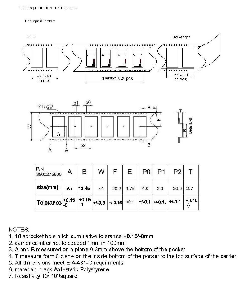
21 Packaging and Reel Information
Figure 33: BT111 reel dimensions
Bluegiga Technologies Oy
Page 53 of 54
Figure 34: Package tape dimensions

Bluegiga Technologies Oy
Page 54 of 54
22 Contact Information
Sales: sales@bluegiga.com
Technical support: www.bluegiga.com
Orders: orders@bluegiga.com
WWW: www.bluegiga.com
www.bluegiga.hk
Head Office / Finland:
Phone: +358-9-4355 060
Fax: +358-9-4355 0660
Sinikalliontie 5A
02630 ESPOO
FINLAND
Postal address / Finland:
P.O. BOX 120
02631 ESPOO
FINLAND
Sales Office / USA:
Phone: +1 770 291 2181
Fax: +1 770 291 2183
Bluegiga Technologies, Inc.
3235 Satellite Boulevard, Building 400, Suite 300
Duluth, GA, 30096, USA
Sales Office / Hong Kong:
Phone: +852 3972 2186
Bluegiga Technologies Ltd.
Unit 10-18
32/F, Tower 1, Millennium City 1
388 Kwun Tong Road
Kwun Tong, Kowloon
Hong Kong