Honeywell VM3WLANA Vehicle Mount Computer User Manual Product Data Sheet
Honeywell International Inc Vehicle Mount Computer Product Data Sheet
Contents
- 1. User Manual_BT111 bluetooth Module
- 2. User Manual_RegSht-VM3 Rev (b)
- 3. User Manual_VM3-W7-UG Rev (a)-1
- 4. User Manual_VM3-W7-UG Rev (a)-2
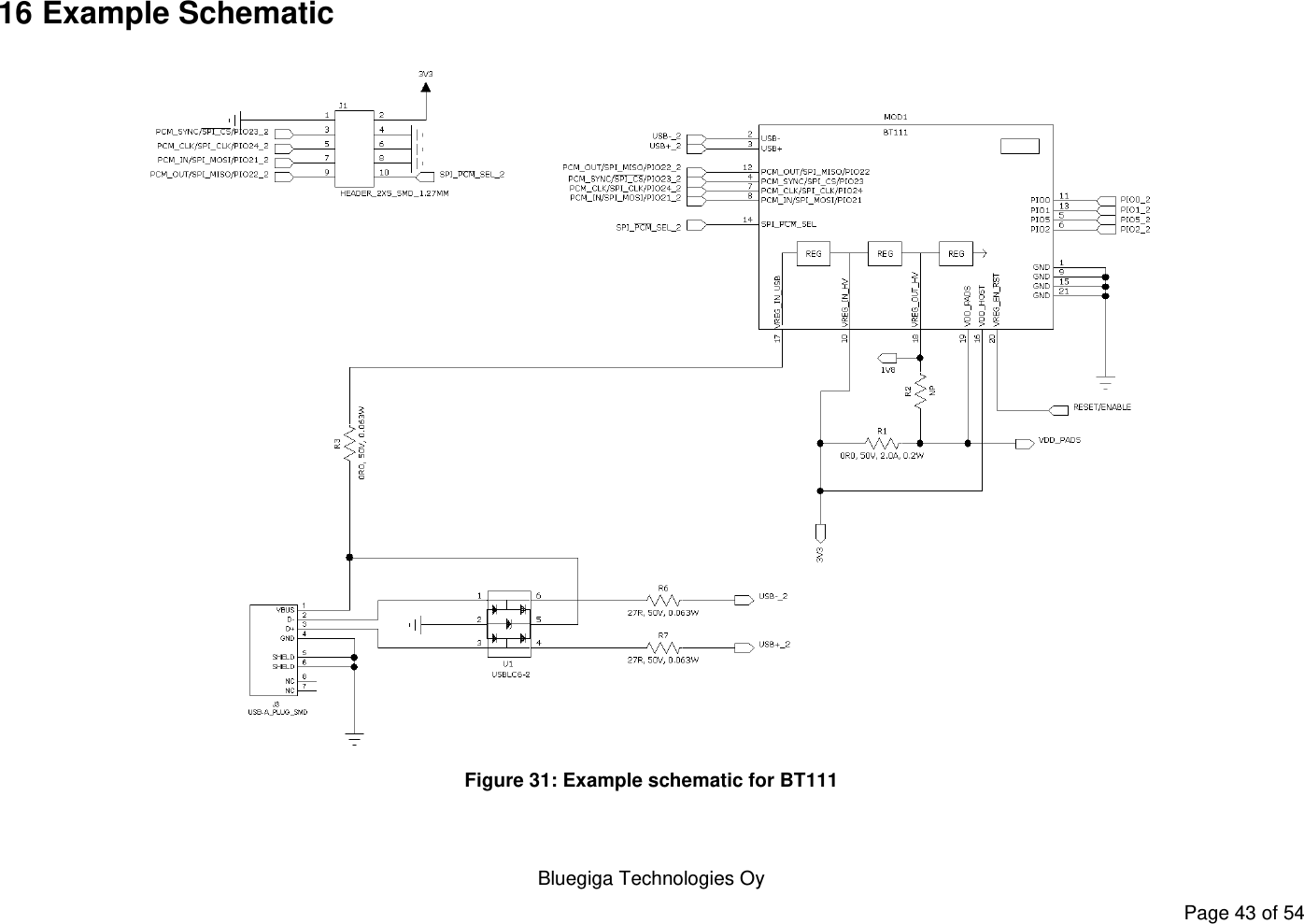
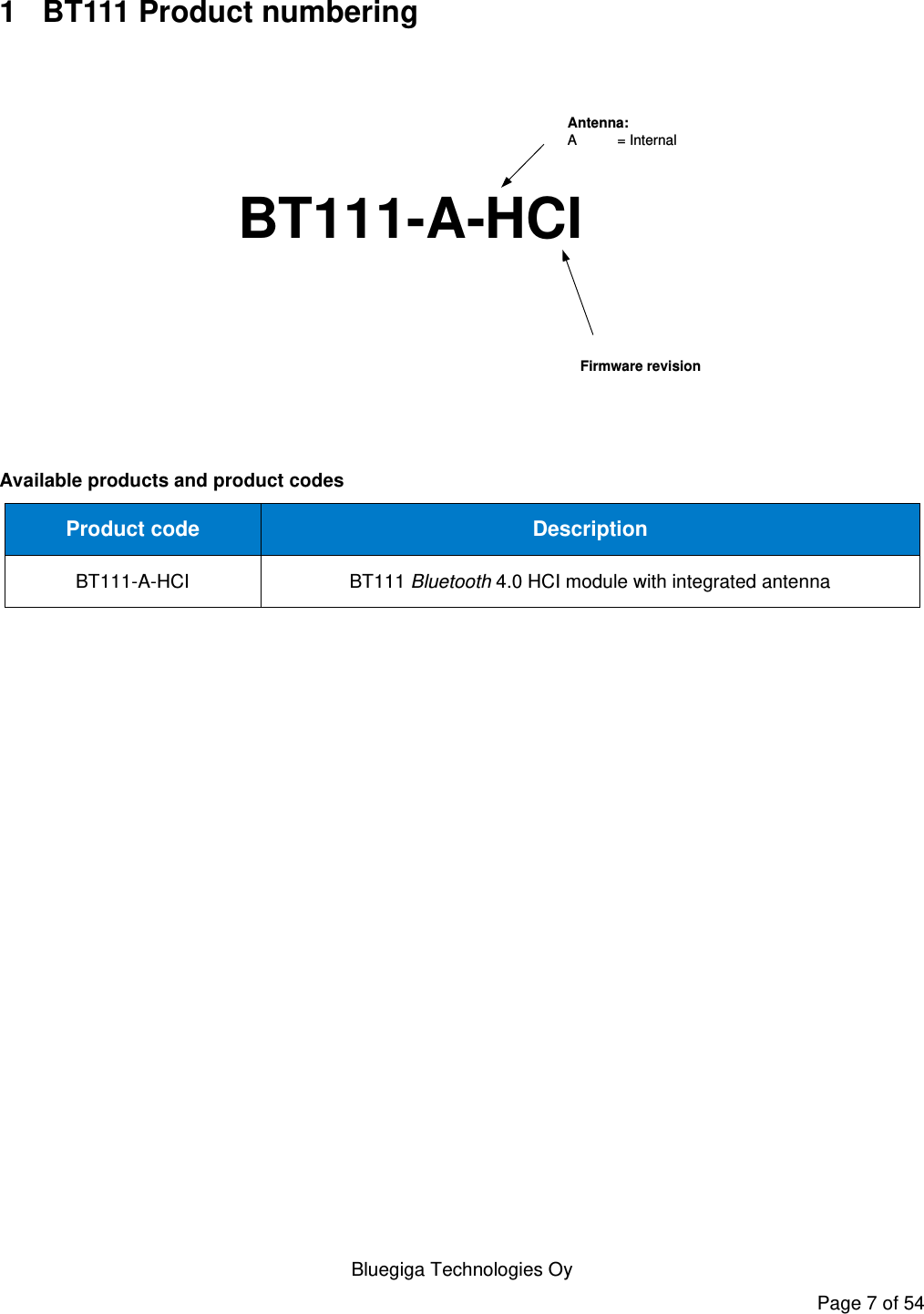
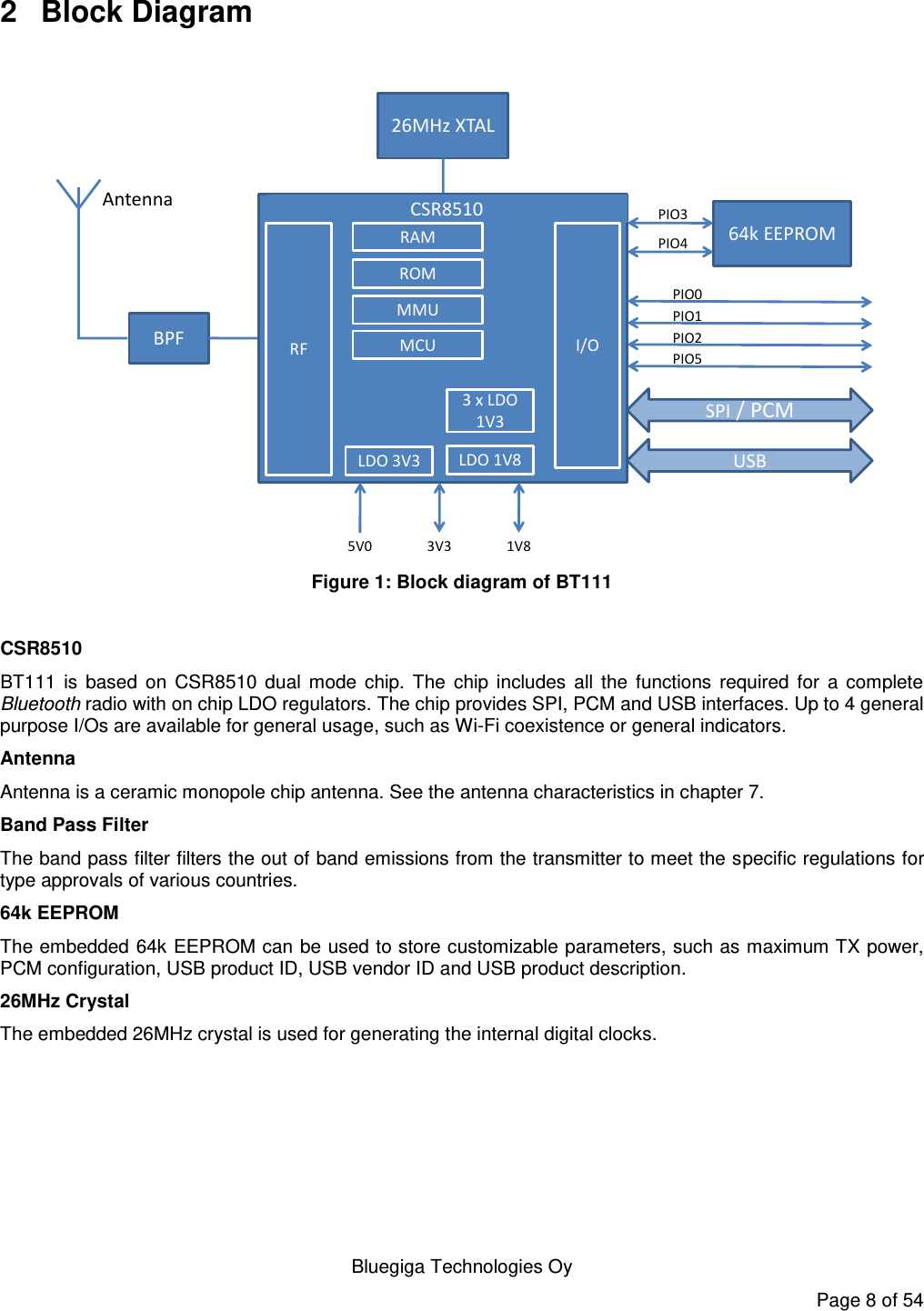
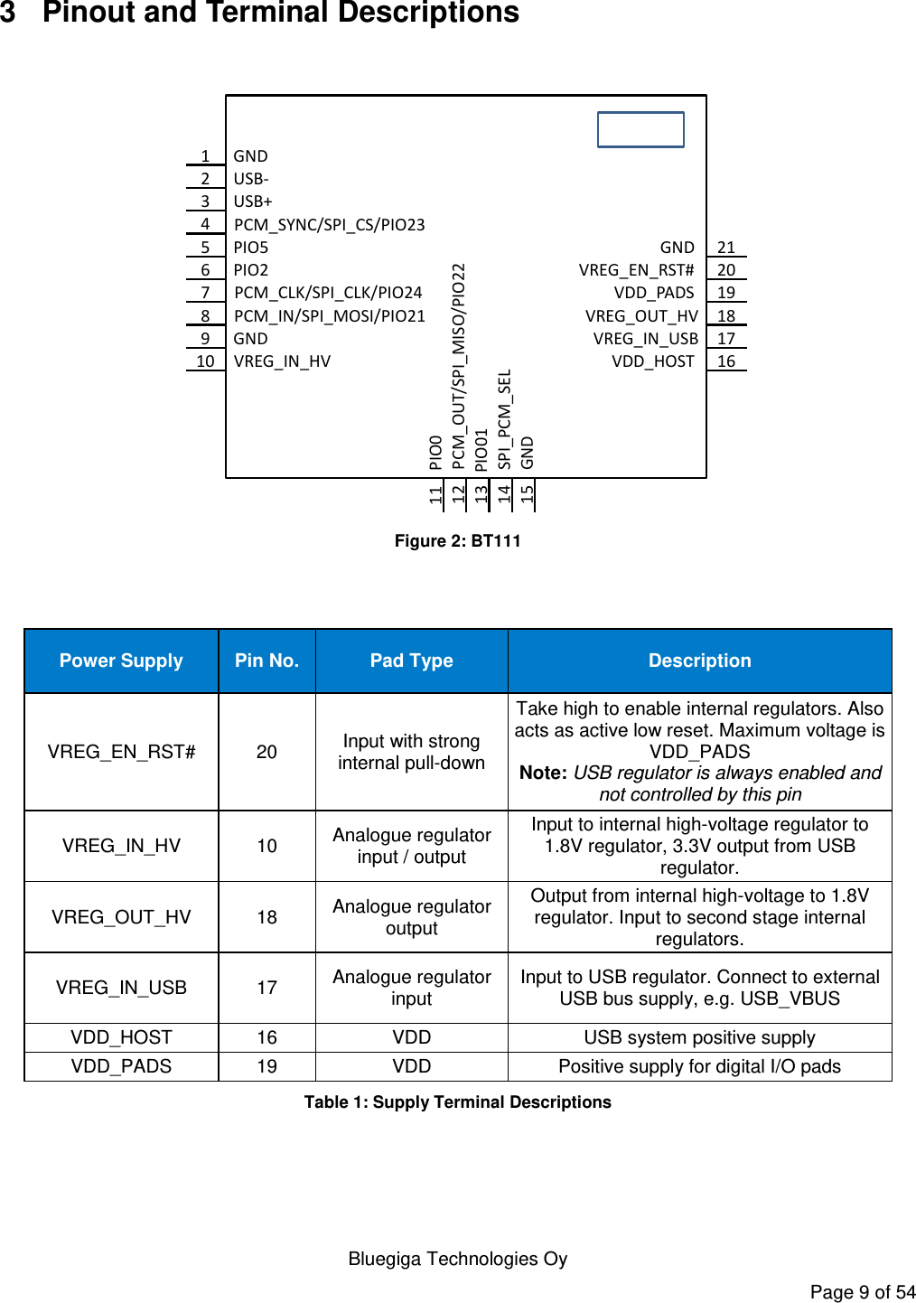
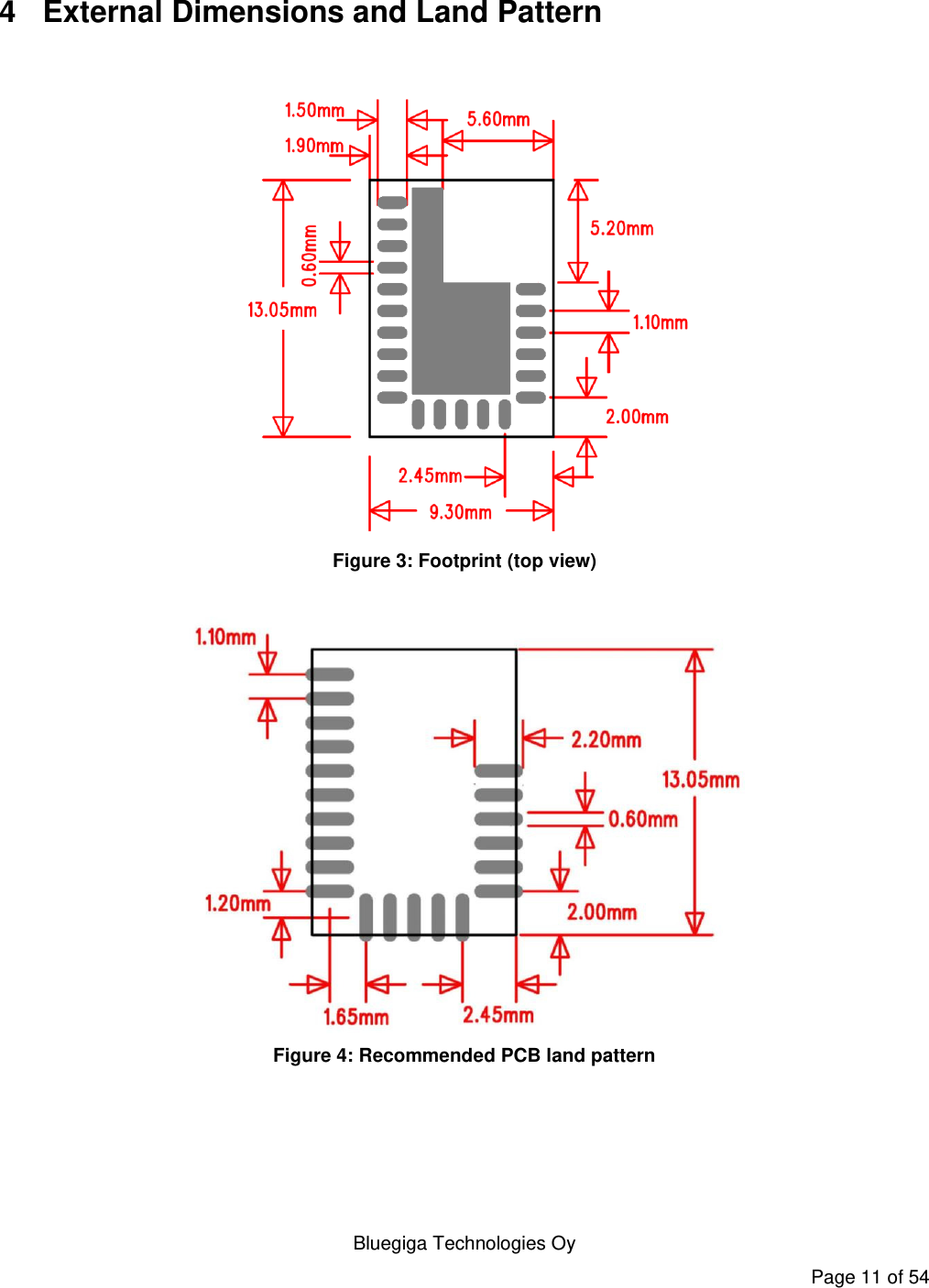
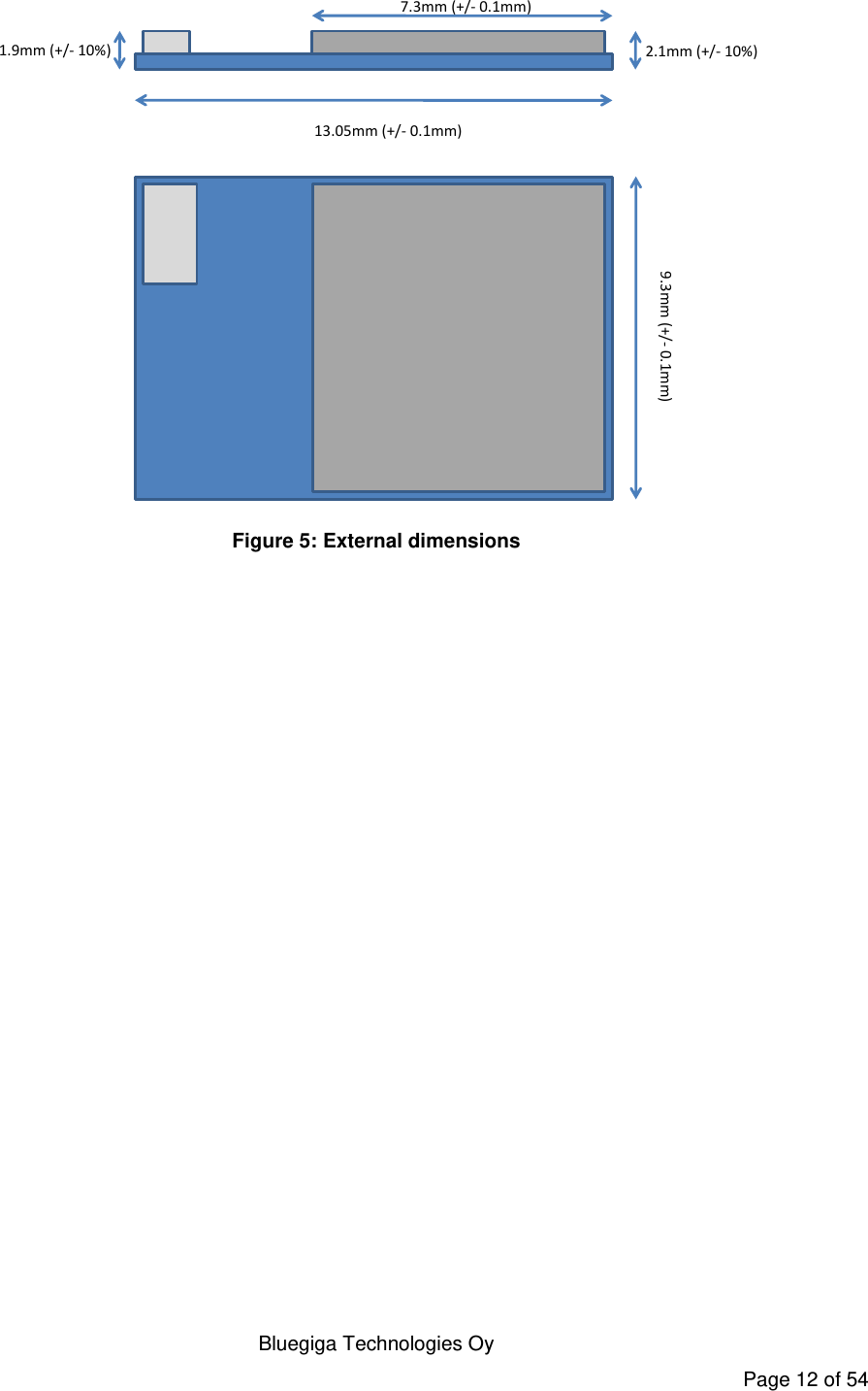
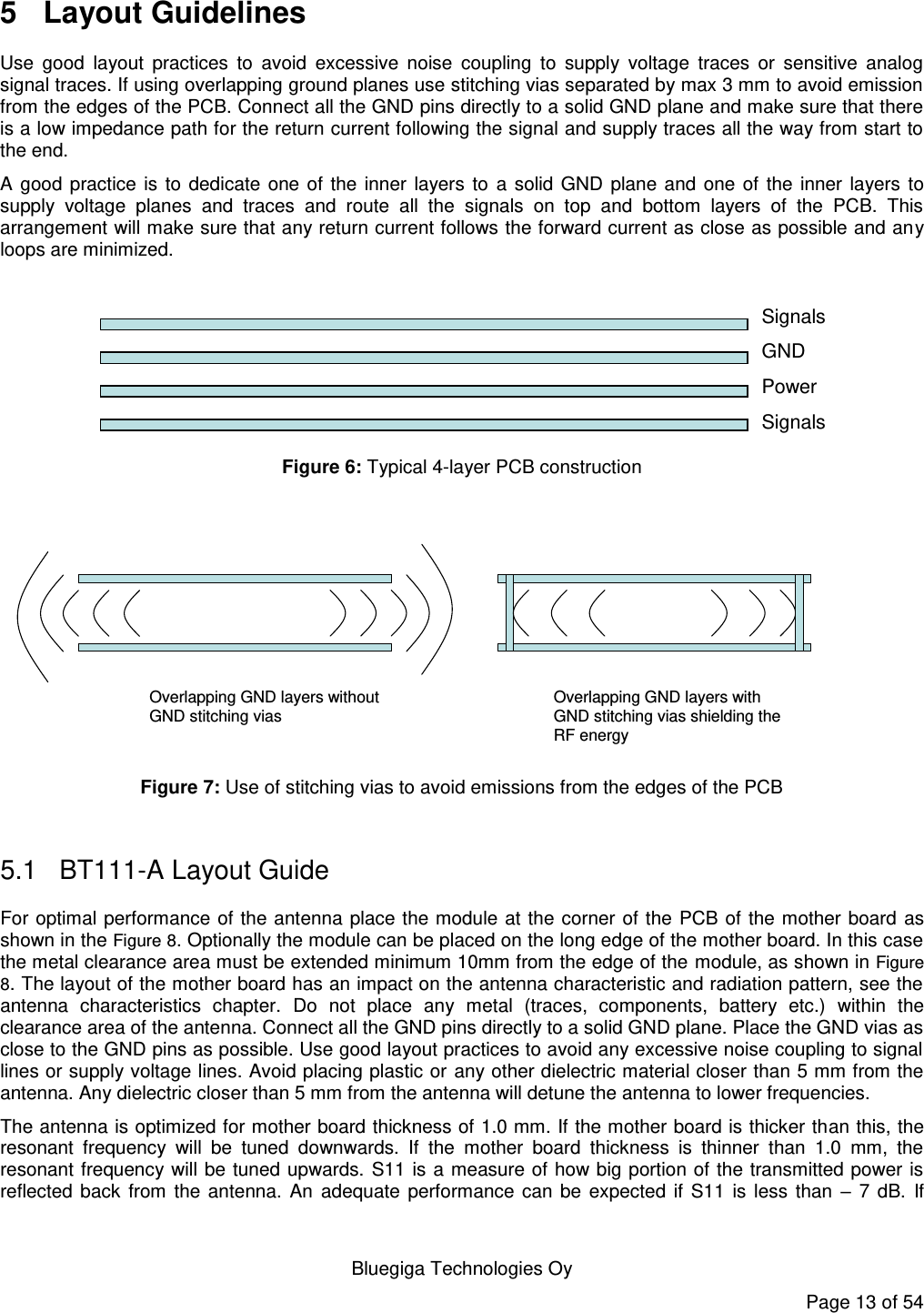
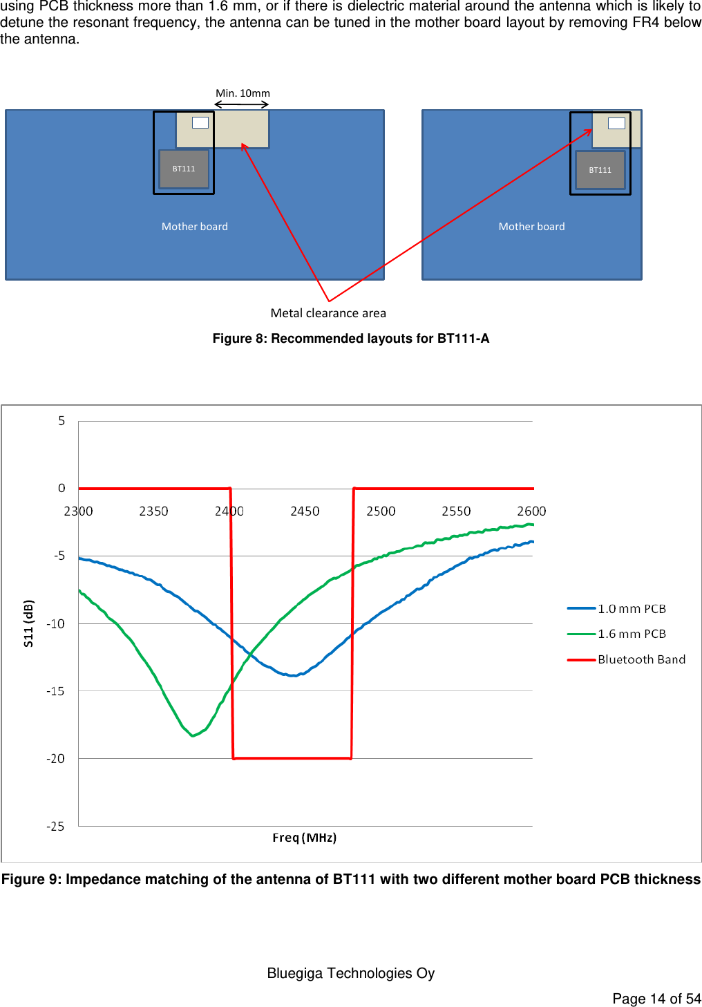
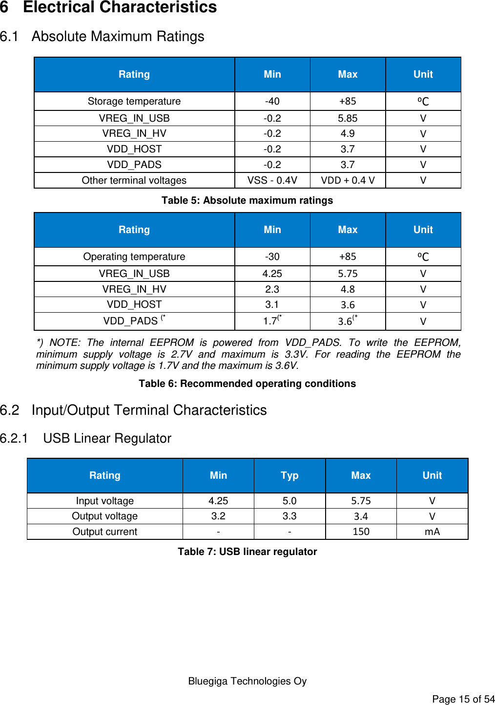
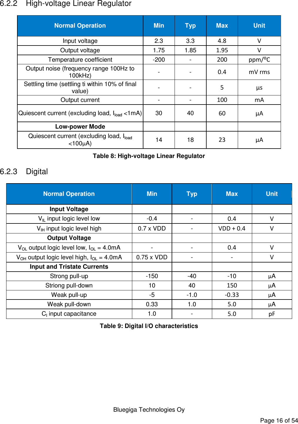
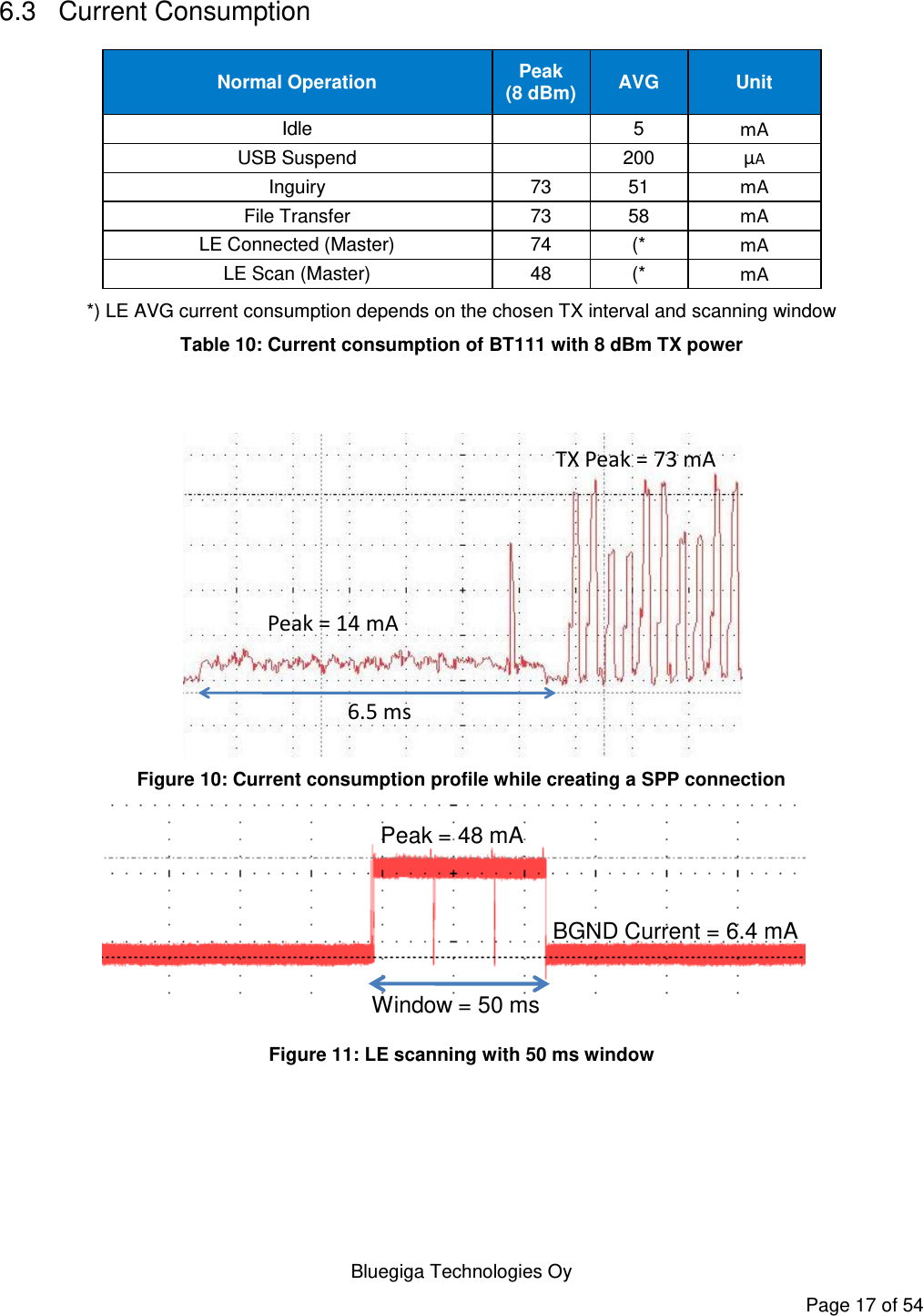
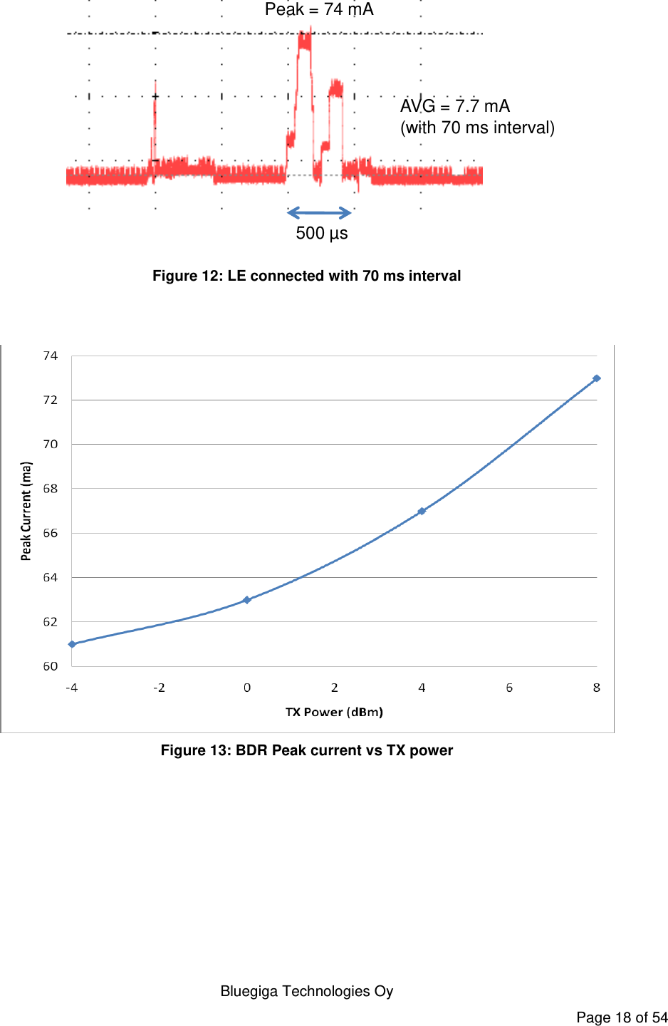
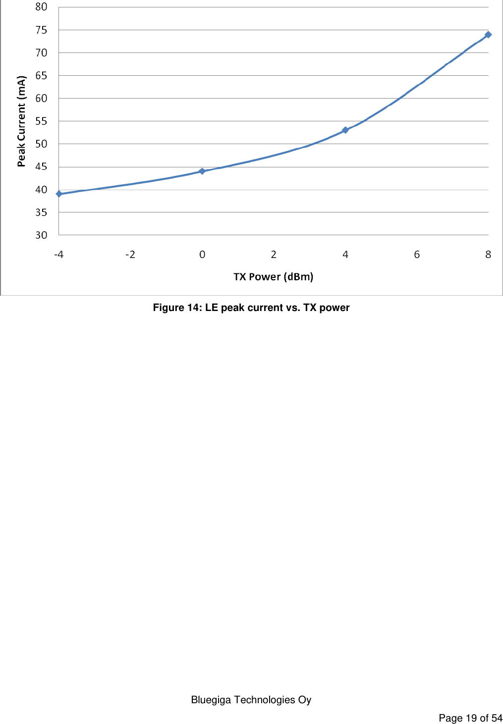
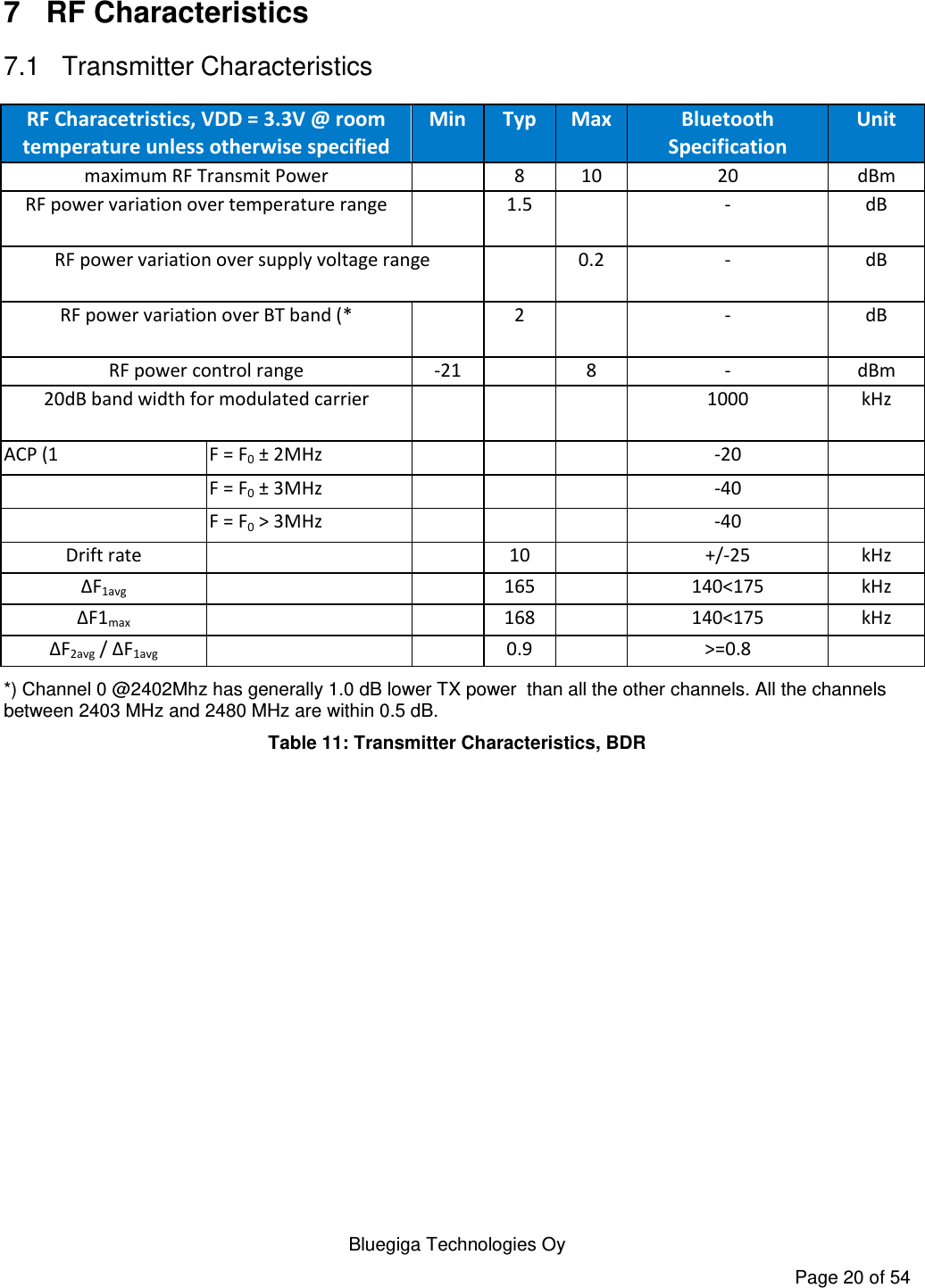
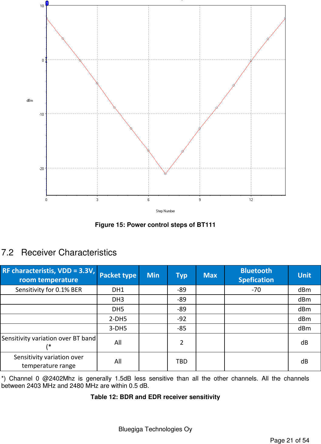
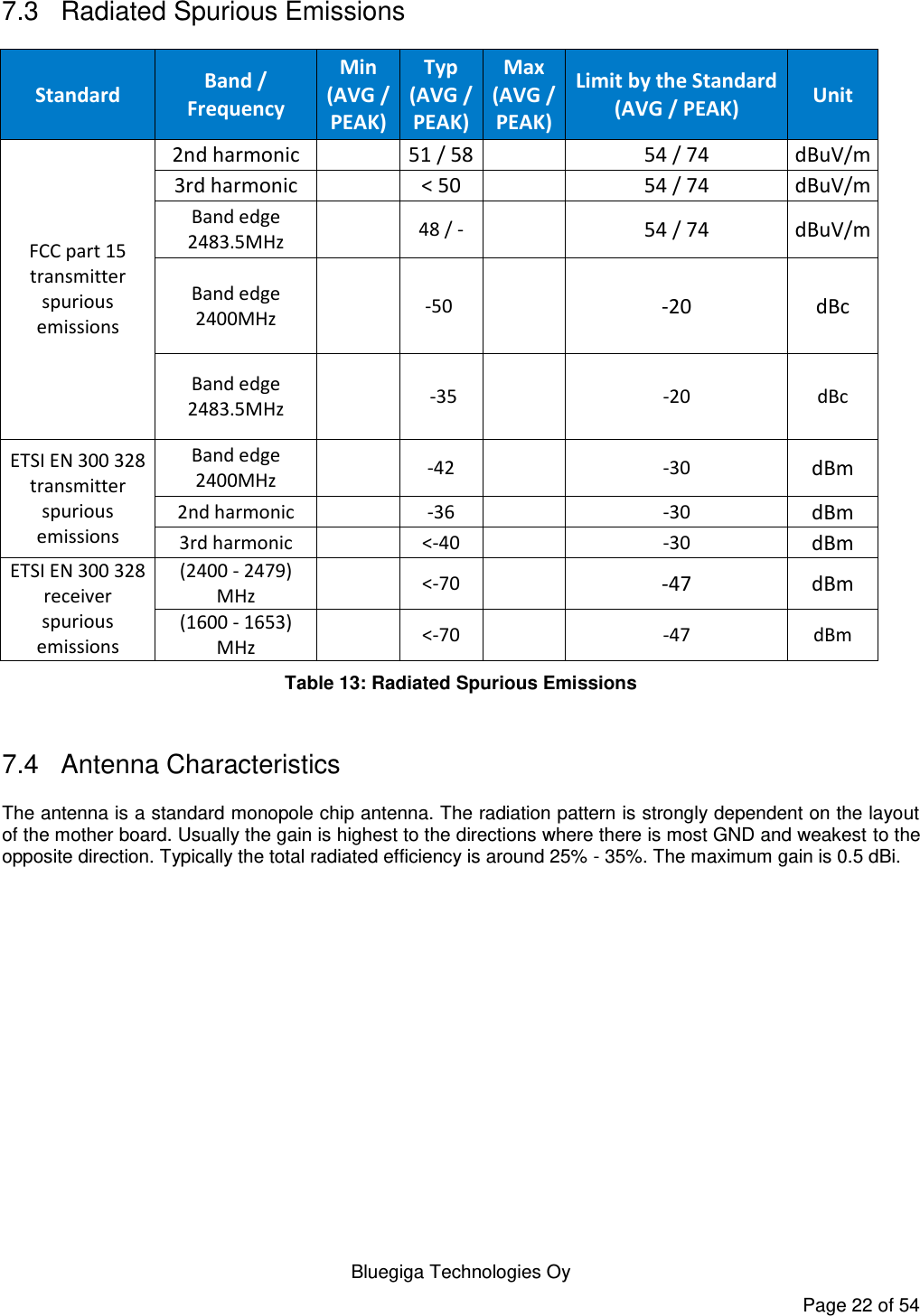
User Manual_BT111 bluetooth Module
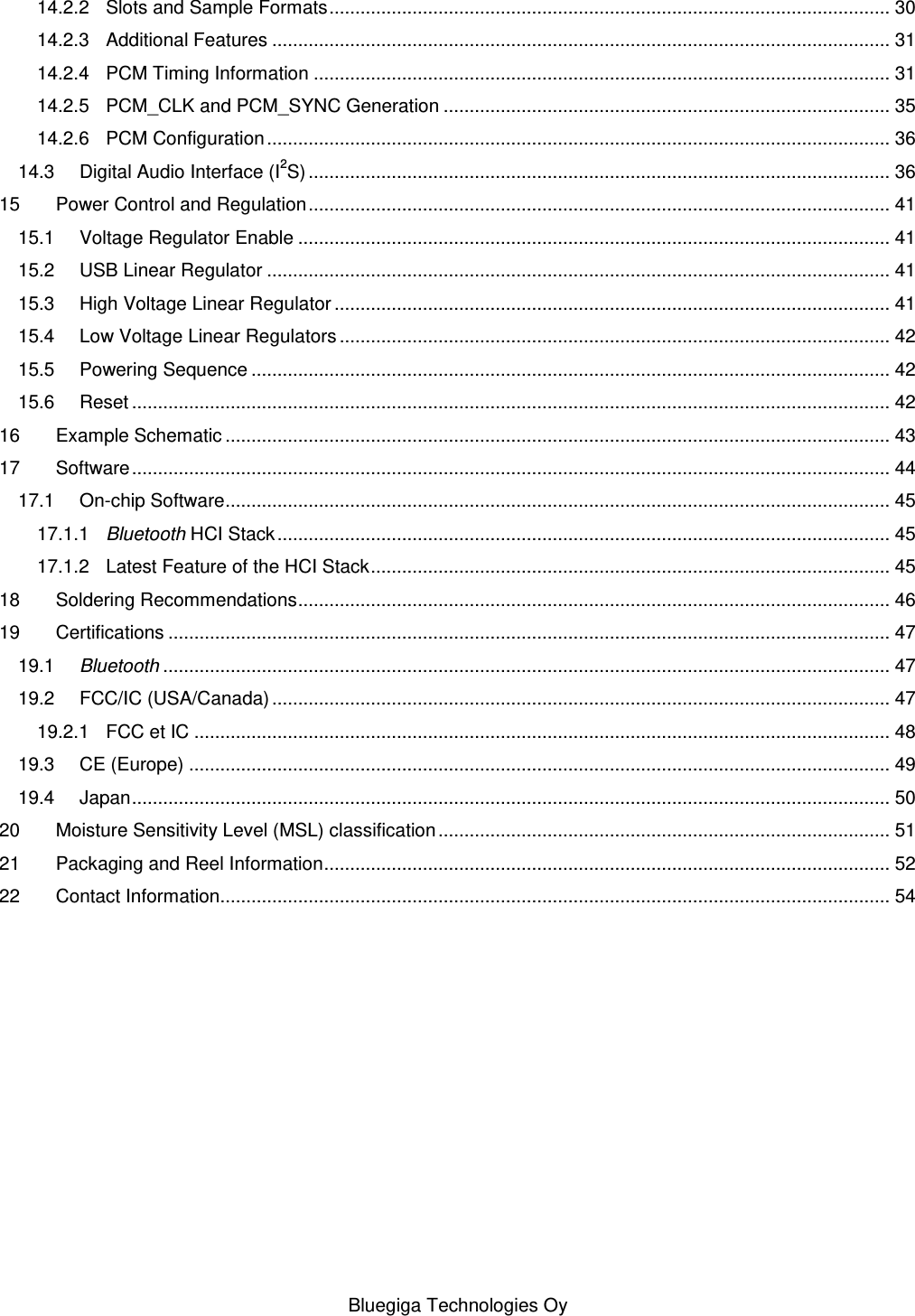

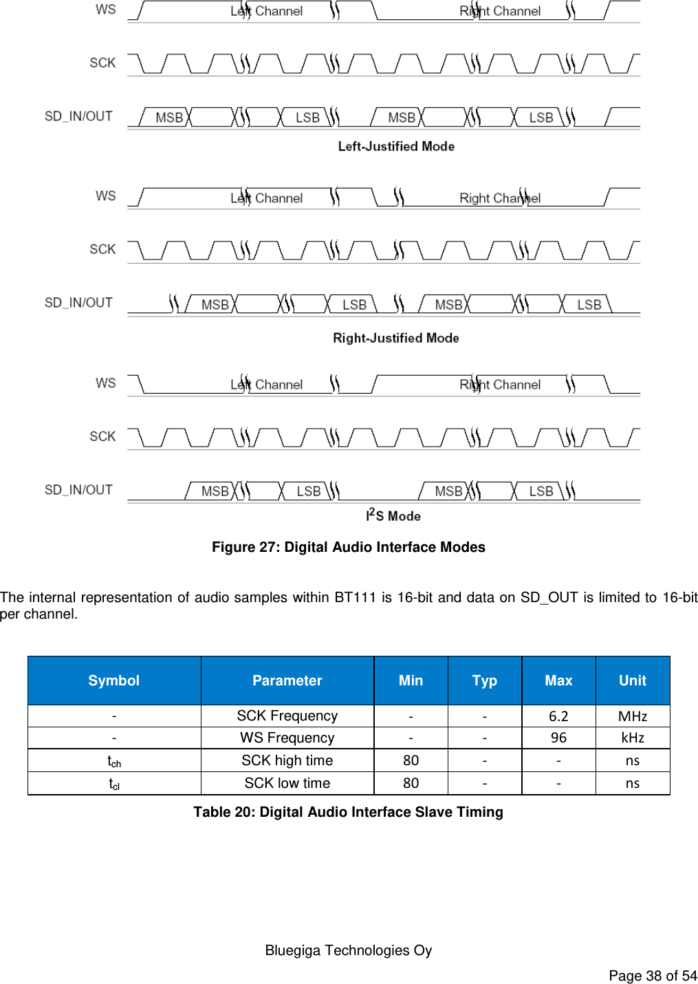
![Bluegiga Technologies Oy Page 37 of 54 Bit Mask Name Description D[0] 0x0001 CONFIG_JUSTIFY_FORMAT 0 for left justified, 1 for right justified D[1] 0x0002 CONFIG_LEFT_JUSTIFY_DELAY For left justified formats: 0 is MSB of SD data occurs in the first SCLK period following WS transition. 1 is MSB of SD data occurs in the second SCLK period. D[2] 0x0004 CONFIG_CHANNEL_POLARITY For 0, SD data is left channel when WS is high. For 1 SD data is right channel. D[3] 0x0008 CONFIG_AUDIO_ATTEN_EN For 0, 17 bit SD data is rounded down to 16 bits. For 1, the audio attenuation defined in CONFIG_AUDIO_ATTEN is applied over 24 bits with saturated rounding. Requires CONFIG_16_BIT_CROP_EN to be 0. D[7:4] 0x00F0 CONFIG_AUDIO_ATTEN Attenuation in 6 dB steps. D[9:8] 0x0300 CONFIG_JUSTIFY_RESOLUTION Resolution of data on SD_IN, 00=16 bit, 01=20 bit, 10=24 bit, 11=Reserved. This is required for right justified format and with left justified LSB first. D[10] 0x0400 CONFIG_16_BIT_CROP_EN For 0, 17 bit SD_IN data is rounded down to 16 bits. For 1 only the most significant 16 bits of data are received. Table 19: PSKEY_DIGITAL_AUDIO_CONFIG](https://usermanual.wiki/Honeywell/VM3WLANA.User-Manual-BT111-bluetooth-Module/User-Guide-2559730-Page-37.png)
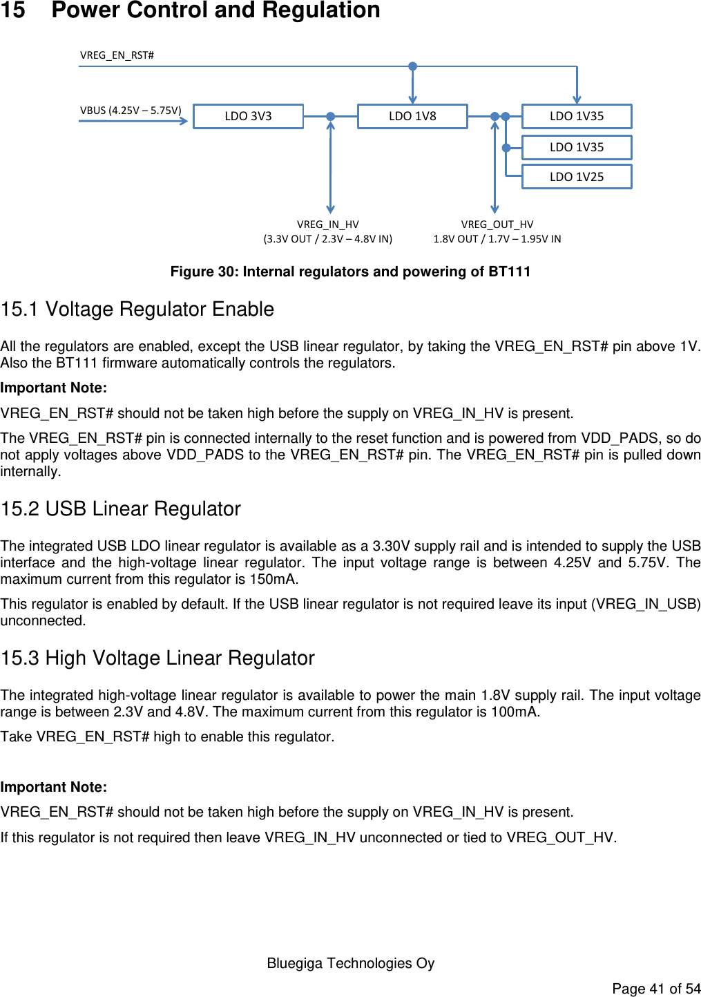
![Bluegiga Technologies Oy Page 42 of 54 15.4 Low Voltage Linear Regulators BT111 has three integrated low voltage linear regulators providing the internal supply voltages for RF and digital circuits of BT111. The input voltage range is between 1.70V and 1.95V. 15.5 Powering Sequence All the power supplies should be powered at the same time. The order of powering the supplies relative to the I/O supply, VDD_PADS to VDD_HOST, is not important. If the I/O supply is powered before VDD_DIG, all digital I/Os are weak pull-downs irrespective of the reset state. 15.6 Reset The reset function is internally tied to the VREG_EN_RST# pin. BT111 is reset from several sources: VREG_EN_RST# pin Power-on reset Via a software-configured watchdog timer The VREG_EN_RST# pin is an active low reset. Assert the reset signal for a period >5ms to ensure a full reset. Important Note: Bluegiga does not recommend assertions of the reset of <5ms on the VREG_EN_RST# pin, as any glitches on this line can affect I/O integrity without triggering a reset. A warm reset function is also available under software control. After a warm reset the RAM data remains available. Pin Name/Group I/O Type No Core Supply Reset Full Chip Reset VREG_EN_RST# Digital input Strong pull-down N/A SPI_CLK/PCM_CLK / PIO[24] Digital bidirectional tristated Weak pull-down Weak pull-down SPI_CS# / PCM_SYNC / PIO[23] Digital bidirectional tristated Weak pull-up (SPI) Weak pull-down (PCM) Weak pull-up (SPI) Weak pull-down (PCM / PIO) SPI_MISO / PCM_OUT / PIO[22] Digital output tristated Weak pull-down Weak pull-down SPI_MOSI / PCM_OUT / PIO[21] Digital input Weak pull-down Weak pull-down PIO[5:0] Digital bidirectional tristated Weak pull-down Weak pull-down Table 24: Digital Pin States on Reset](https://usermanual.wiki/Honeywell/VM3WLANA.User-Manual-BT111-bluetooth-Module/User-Guide-2559730-Page-42.png)