Huawei ME909s Series LTE LGA Module Hardware Guide (V100R001 04, English)
2016-12-28
User Manual: Huawei
Open the PDF directly: View PDF ![]() .
.
Page Count: 101 [warning: Documents this large are best viewed by clicking the View PDF Link!]
- Copyright © Huawei Technologies Co., Ltd. 2016. All rights reserved.
- Trademarks and Permissions
- Notice
- DISCLAIMER
- Import and Export Regulations
- Privacy Policy
- Revision History
- Scope
- 1 Introduction
- 2 Overall Description
- 3 Description of the Application Interfaces
- 3.1 About This Chapter
- 3.2 LGA Interface
- 3.3 Power Interface
- 3.4 Signal Control Interface
- 3.5 UART Interface
- 3.6 USB Interface
- 3.7 USIM Card Interface
- 3.8 Audio Interface
- 3.9 GPIO Interface
- 3.10 ADC Interface
- 3.11 JTAG Interface
- 3.12 RF Antenna Interface
- Table 3-16 Definition of the antenna pads
- Figure 3-25 RF signal trace design about MAIN_ANT for reference (the same for AUX_ANT)
- Figure 3-26 RF signal layout design about MAIN_ANT for reference (the same for AUX_ANT)
- Figure 3-27 Complete structure of the microstrip
- Figure 3-28 Complete structure of the stripline
- Figure 3-29 Pad for the RF interface
- Figure 3-30 RF Pad design for ME909s LGA
- 3.13 Reserved Interface
- 3.14 NC Interface
- 3.15 Test Points Design
- 4 RF Specifications
- 4.1 About This Chapter
- 4.2 Operating Frequencies
- 4.3 Conducted RF Measurement
- 4.4 Conducted Rx Sensitivity and Tx Power
- 4.5 Antenna Design Requirements
- 4.6 Suggestions about LTE and 2.4 GHz Wi-Fi Co-existence
- 4.6.1 Theory Analysis
- 4.6.2 Suggestions about the Interference
- 1. It is recommended that the system should be added Wi-Fi SAW filter to guarantee good attenuation in the LTE transmit Band (including Band 38, Band 40, Band 41), otherwise, LTE Band output power will block Wi-Fi receiver.
- 2. The good isolation between LTE antenna and Wi-Fi antenna is more than 25 dB.
- 3. Two ways above can help to make the isolation to be 60 dB. If they are still not enough, some channels may need to be disabled.
- 5 Electrical and Reliability Features
- 5.1 About This Chapter
- 5.2 Absolute Ratings
- 5.3 Operating and Storage Temperatures
- 5.4 Power Supply Features
- 5.4.1 Input Power Supply
- 5.4.2 Power Consumption
- Table 5-5 Averaged power off DC power consumption
- Table 5-6 Averaged standby DC power consumption of ME909s-821 LGA module
- Table 5-7 Averaged standby DC power consumption of ME909s-120 LGA module
- Table 5-8 Averaged Data Transmission DC power consumption of ME909s-821 LGA module (LTE/HSPA/WCDMA/TD-SCDMA)
- Table 5-9 Averaged Data Transmission DC power consumption of ME909s-120 LGA module (WCDMA/HSDPA/LTE)
- Table 5-10 Averaged DC power consumption of ME909s-821 LGA module (GPRS/EDGE)
- Table 5-11 Averaged DC power consumption of ME909s-120 LGA module (GPRS/EDGE)
- 5.5 Reliability Features
- 5.6 EMC and ESD Features
- 6 Mechanical Specifications
- 6.1 About This Chapter
- 6.2 Storage Requirement
- 6.3 Moisture Sensitivity
- 6.4 Dimensions
- 6.5 Packaging
- 6.6 Customer PCB Design
- 6.7 Thermal Design Solution
- 6.8 Assembly Processes
- 6.9 Specification of Rework
- 6.9.1 Process of Rework
- 6.9.2 Preparations of Rework
- 6.9.3 Removing of the Module
- 6.9.4 Welding Area Treatment
- Step 1 Remove the old solder by using a soldering iron and solder braid that can wet the solder.
- Step 2 Clean the pad and remove the flux residuals.
- Step 3 Solder pre-filling: Before the module is installed on a board, apply some solder paste to the pad of the module by using the rework fixture and stencil or apply some solder paste to the pad on the PCB by using a rework stencil.
- 6.9.5 Module Installation
- 6.9.6 Specifications of Rework
- 7 Certifications
- 8 Safety Information
- 8.1 About This Chapter
- 8.2 Interference
- 8.3 Medical Device
- 8.4 Area with Inflammables and Explosives
- 8.5 Traffic Security
- 8.6 Airline Security
- 8.7 Safety of Children
- 8.8 Environment Protection
- 8.9 WEEE Approval
- 8.10 RoHS Approval
- 8.11 Laws and Regulations Observance
- 8.12 Care and Maintenance
- 8.13 Emergency Call
- 8.14 Regulatory Information
- 9 Appendix A Circuit of Typical Interface
- 10 Appendix B Acronyms and Abbreviations

HUAWEI ME909s Series LTE LGA Module
Hardware Guide
Issue
04
Date
2016-12-21

Copyright © Huawei Technologies Co., Ltd. 2016. All rights reserved.
No part of this manual may be reproduced or transmitted in any form or by any means without prior written
consent of Huawei Technologies Co., Ltd. and its affiliates ("Huawei").
The product described in this manual may include copyrighted software of Huawei and possible licensors.
Customers shall not in any manner reproduce, distribute, modify, decompile, disassemble, decrypt, extract,
reverse engineer, lease, assign, or sublicense the said software, unless such restrictions are prohibited by
applicable laws or such actions are approved by respective copyright holders.
Trademarks and Permissions
, , and are trademarks or registered trademarks of Huawei Technologies Co., Ltd.
LTE is a trade mark of ETSI.
Other trademarks, product, service and company names mentioned may be the property of their respective
owners.
Notice
Some features of the product and its accessories described herein rely on the software installed, capacities
and settings of local network, and therefore may not be activated or may be limited by local network operators
or network service providers.
Thus, the descriptions herein may not exactly match the product or its accessories which you purchase.
Huawei reserves the right to change or modify any information or specifications contained in this manual
without prior notice and without any liability.
DISCLAIMER
ALL CONTENTS OF THIS MANUAL ARE PROVIDED “AS IS”. EXCEPT AS REQUIRED BY APPLICABLE
LAWS, NO WARRANTIES OF ANY KIND, EITHER EXPRESS OR IMPLIED, INCLUDING BUT NOT
LIMITED TO, THE IMPLIED WARRANTIES OF MERCHANTABILITY AND FITNESS FOR A PARTICULAR
PURPOSE, ARE MADE IN RELATION TO THE ACCURACY, RELIABILITY OR CONTENTS OF THIS
MANUAL.
TO THE MAXIMUM EXTENT PERMITTED BY APPLICABLE LAW, IN NO EVENT SHALL HUAWEI BE
LIABLE FOR ANY SPECIAL, INCIDENTAL, INDIRECT, OR CONSEQUENTIAL DAMAGES, OR LOSS OF
PROFITS, BUSINESS, REVENUE, DATA, GOODWILL SAVINGS OR ANTICIPATED SAVINGS
REGARDLESS OF WHETHER SUCH LOSSES ARE FORSEEABLE OR NOT.
THE MAXIMUM LIABILITY (THIS LIMITATION SHALL NOT APPLY TO LIABILITY FOR PERSONAL
INJURY TO THE EXTENT APPLICABLE LAW PROHIBITS SUCH A LIMITATION) OF HUAWEI ARISING
FROM THE USE OF THE PRODUCT DESCRIBED IN THIS MANUAL SHALL BE LIMITED TO THE
AMOUNT PAID BY CUSTOMERS FOR THE PURCHASE OF THIS PRODUCT.
Import and Export Regulations
Customers shall comply with all applicable export or import laws and regulations and be responsible to obtain
all necessary governmental permits and licenses in order to export, re-export or import the product mentioned
in this manual including the software and technical data therein.
Privacy Policy
To better understand how we protect your personal information, please see the privacy policy at
http://consumer.huawei.com/privacy-policy.
HUAWEI ME909s Series LTE LGA Module
Hardware Guide
About This Document
Issue 04 (2016-12-21)
Huawei Proprietary and Confidential
Copyright © Huawei Technologies Co., Ltd.
3
About This Document
Revision History
Document
Version
Date
Chapter
Descriptions
01
2015-08-14
Initial release
02
2016-02-20
2.4
Deleted Application Block Diagram
2.2
Updated Table 2-1 Features
3.2
Updated LGA Interface
3.5
Updated UART Interface
3.9
Updated GPIO Interface
4.2
Updated the NOTE of Operating
Frequencies
4.5.3
Updated Antenna Requirements
5.6
Updated EMC and ESD Features
6.5
Updated Packaging
03
2016-09-06
2
Updated Table 2-1 Features
3.2
Updated Figure 3-1 Sequence of LGA
interface (Top view)
3.4.8
Updated Figure 3-15 Connections of the
USIM_DET pin
3.7
Updated Figure 3-19 Circuit of the USIM
card interface
5.4.2
Updated Table 5-6 Averaged standby DC
power consumption of ME909s-821 LGA
module
6.6.2
Updated Figure 6-4 LGA module Footprint
design (Unit: mm)
6.8.2
Updated Figure 6-8 Recommended stencil
design of LGA module (Unit: mm)
HUAWEI ME909s Series LTE LGA Module
Hardware Guide
About This Document
Issue 04 (2016-12-21)
Huawei Proprietary and Confidential
Copyright © Huawei Technologies Co., Ltd.
4
Document
Version
Date
Chapter
Descriptions
6.9.3
Updated Figure 6-10 Equipment used for
rework
04
2016-12-21
3.2
Updated Table 3-1 Definitions of pins on the
LGA interface
5.5
Updated Table 5-12 Test conditions and
results of the reliability of the ME909s LGA
module
Scope
ME909s-821
ME909s-120
HUAWEI ME909s Series LTE LGA Module
Hardware Guide
Contents
Issue 04 (2016-12-21)
Huawei Proprietary and Confidential
Copyright © Huawei Technologies Co., Ltd.
5
Contents
1 Introduction ........................................................................................................................... 8
2 Overall Description ............................................................................................................... 9
2.1 About This Chapter.......................................................................................................................... 9
2.2 Function Overview .......................................................................................................................... 9
2.3 Circuit Block Diagram .................................................................................................................... 11
3 Description of the Application Interfaces ......................................................................... 13
3.1 About This Chapter........................................................................................................................ 13
3.2 LGA Interface ................................................................................................................................ 13
3.3 Power Interface ............................................................................................................................. 24
3.3.1 Overview............................................................................................................................... 24
3.3.2 Power Supply VBAT Interface............................................................................................... 25
3.3.3 Output Power Supply Interface ............................................................................................. 27
3.4 Signal Control Interface ................................................................................................................. 27
3.4.1 Overview............................................................................................................................... 27
3.4.2 Power-on/off Pin ................................................................................................................... 29
3.4.3 RESIN_N .............................................................................................................................. 31
3.4.4 WAKEUP_IN Signal .............................................................................................................. 32
3.4.5 WAKEUP_OUT Signal .......................................................................................................... 33
3.4.6 SLEEP_STATUS Signal........................................................................................................ 33
3.4.7 LED_MODE Signal ............................................................................................................... 34
3.4.8 USIM_DET Pin ..................................................................................................................... 35
3.5 UART Interface.............................................................................................................................. 37
3.5.1 Overview............................................................................................................................... 37
3.5.2 Circuit Recommended for the UART Interface...................................................................... 38
3.6 USB Interface ................................................................................................................................ 39
3.7 USIM Card Interface ..................................................................................................................... 40
3.7.1 Overview............................................................................................................................... 40
3.7.2 Circuit Recommended for the USIM Card Interface.............................................................. 41
3.8 Audio Interface .............................................................................................................................. 42
3.9 GPIO Interface .............................................................................................................................. 44
3.10 ADC Interface .............................................................................................................................. 47
3.11 JTAG Interface............................................................................................................................. 47

HUAWEI ME909s Series LTE LGA Module
Hardware Guide
Contents
Issue 04 (2016-12-21)
Huawei Proprietary and Confidential
Copyright © Huawei Technologies Co., Ltd.
6
3.12 RF Antenna Interface .................................................................................................................. 48
3.13 Reserved Interface ...................................................................................................................... 51
3.14 NC Interface ................................................................................................................................ 51
3.15 Test Points Design....................................................................................................................... 52
4 RF Specifications ................................................................................................................. 53
4.1 About This Chapter........................................................................................................................ 53
4.2 Operating Frequencies .................................................................................................................. 53
4.3 Conducted RF Measurement ........................................................................................................ 55
4.3.1 Test Environment .................................................................................................................. 55
4.3.2 Test Standards ...................................................................................................................... 55
4.4 Conducted Rx Sensitivity and Tx Power ....................................................................................... 55
4.4.1 Conducted Receive Sensitivity ............................................................................................. 55
4.4.2 Conducted Transmit Power .................................................................................................. 57
4.5 Antenna Design Requirements ...................................................................................................... 58
4.5.1 Antenna Design Indicators .................................................................................................... 58
4.5.2 Interference .......................................................................................................................... 61
4.5.3 Antenna Requirements ......................................................................................................... 61
4.6 Suggestions about LTE and 2.4 GHz Wi-Fi Co-existence ............................................................. 62
4.6.1 Theory Analysis .................................................................................................................... 62
4.6.2 Suggestions about the Interference ...................................................................................... 63
5 Electrical and Reliability Features ..................................................................................... 64
5.1 About This Chapter........................................................................................................................ 64
5.2 Absolute Ratings ........................................................................................................................... 64
5.3 Operating and Storage Temperatures ........................................................................................... 64
5.4 Power Supply Features ................................................................................................................. 65
5.4.1 Input Power Supply............................................................................................................... 65
5.4.2 Power Consumption ............................................................................................................. 66
5.5 Reliability Features ........................................................................................................................ 75
5.6 EMC and ESD Features ................................................................................................................ 78
6 Mechanical Specifications .................................................................................................. 81
6.1 About This Chapter........................................................................................................................ 81
6.2 Storage Requirement .................................................................................................................... 81
6.3 Moisture Sensitivity ....................................................................................................................... 81
6.4 Dimensions ................................................................................................................................... 82
6.5 Packaging ..................................................................................................................................... 82
6.6 Customer PCB Design .................................................................................................................. 85
6.6.1 PCB Surface Finish .............................................................................................................. 85
6.6.2 PCB Pad Design ................................................................................................................... 85
6.6.3 Solder Mask .......................................................................................................................... 85
6.6.4 Requirements on PCB Layout .............................................................................................. 85
6.7 Thermal Design Solution ............................................................................................................... 86

HUAWEI ME909s Series LTE LGA Module
Hardware Guide
Contents
Issue 04 (2016-12-21)
Huawei Proprietary and Confidential
Copyright © Huawei Technologies Co., Ltd.
7
6.8 Assembly Processes ..................................................................................................................... 88
6.8.1 General Description of Assembly Processes ........................................................................ 88
6.8.2 Stencil Design ....................................................................................................................... 88
6.8.3 Reflow Profile ....................................................................................................................... 89
6.9 Specification of Rework ................................................................................................................. 90
6.9.1 Process of Rework................................................................................................................ 90
6.9.2 Preparations of Rework ........................................................................................................ 91
6.9.3 Removing of the Module ....................................................................................................... 91
6.9.4 Welding Area Treatment ....................................................................................................... 92
6.9.5 Module Installation ................................................................................................................ 92
6.9.6 Specifications of Rework....................................................................................................... 92
7 Certifications ........................................................................................................................ 93
7.1 About This Chapter........................................................................................................................ 93
7.2 Certifications ................................................................................................................................. 93
8 Safety Information .............................................................................................................. 94
8.1 About This Chapter........................................................................................................................ 94
8.2 Interference ................................................................................................................................... 94
8.3 Medical Device .............................................................................................................................. 94
8.4 Area with Inflammables and Explosives ........................................................................................ 95
8.5 Traffic Security .............................................................................................................................. 95
8.6 Airline Security .............................................................................................................................. 95
8.7 Safety of Children .......................................................................................................................... 95
8.8 Environment Protection ................................................................................................................. 96
8.9 WEEE Approval............................................................................................................................. 96
8.10 RoHS Approval............................................................................................................................ 96
8.11 Laws and Regulations Observance ............................................................................................. 96
8.12 Care and Maintenance ................................................................................................................ 96
8.13 Emergency Call ........................................................................................................................... 97
8.14 Regulatory Information ................................................................................................................ 97
8.14.1 CE Approval (European Union) .......................................................................................... 97
9 Appendix A Circuit of Typical Interface ........................................................................... 98
10 Appendix B Acronyms and Abbreviations ..................................................................... 99

HUAWEI ME909s Series LTE LGA Module
Hardware Guide
Introduction
Issue 04 (2016-12-21)
Huawei Proprietary and Confidential
Copyright © Huawei Technologies Co., Ltd.
8
1 Introduction
This document describes the hardware application interfaces and air interfaces
provided by HUAWEI ME909s Series (ME909s-821 and ME909s-120) LTE LGA
Module (hereinafter referred to as the ME909s LGA module).
This document helps hardware engineer to understand the interface specifications,
electrical features and related product information of the ME909s LGA module.
HUAWEI ME909s Series LTE LGA Module
Hardware Guide
Overall Description
Issue 04 (2016-12-21)
Huawei Proprietary and Confidential
Copyright © Huawei Technologies Co., Ltd.
9
2 Overall Description
2.1 About This Chapter
This chapter gives a general description of the ME909s LGA module and provides:
- Function Overview
- Circuit Block Diagram
2.2 Function Overview
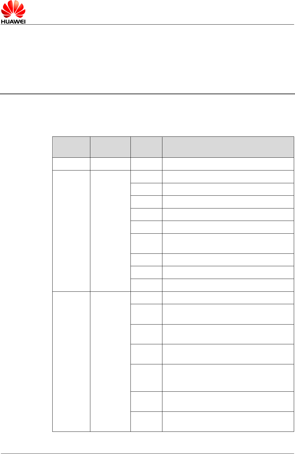
Table 2-1 Features
Feature
Description
Physical
Dimensions
ME909s-821
- Dimensions (L × W × H): 30 mm × 30 mm × 2.57 mm
- Weight: about 5 g
ME909s-120
- Dimensions (L × W × H): 30 mm × 30 mm × 2.52 mm
- Weight: about 5 g
Operating
Bands
ME909s-821
- FDD LTE: Band 1, Band 3, Band 8, all bands with diversity
- TDD LTE: Band 38, Band 39, Band 40, Band 41, all bands with
diversity
- DC-HSPA+/HSPA+/HSPA/WCDMA: Band 1, Band 5, Band 8,
Band 9, all bands with diversity
- TD-SCDMA: Band 34, Band 39
- GSM/GPRS/EDGE: 1800 MHz/900 MHz
HUAWEI ME909s Series LTE LGA Module
Hardware Guide
Overall Description
Issue 04 (2016-12-21)
Huawei Proprietary and Confidential
Copyright © Huawei Technologies Co., Ltd.
10
Feature
Description
ME909s-120
- FDD LTE: Band 1, Band 2, Band 3, Band 4, Band 5, Band 7,
Band 8, Band 20, all bands with diversity
- WCDMA/HSDPA/HSUPA/HSPA+: Band 1, Band 2, Band 5,
Band 8, all bands with diversity
- GSM/GPRS/EDGE: 850 MHz/900 MHz/1800 MHz/1900 MHz
Operating
Temperature
Normal operating temperature: –30°C to +75°C
Extended operating temperature[1]: –40°C to +85°C
Storage
Temperature
–40°C to +85°C
Humidity
RH5% to RH95%
Power
Voltage
DC 3.2 V to 4.2 V (typical value is 3.8 V)
AT
Commands
See the HUAWEI ME909s Series LTE Module AT Command
Interface Specification.
Application
Interface
(145-pin LGA
interface)
One standard USIM (Class B and Class C) interface
Audio interface: PCM interface
USB 2.0 (High Speed)
UART interface:
- 8-wire UART0 x 1
- 2-wire UART2 x 1 (This is only used for debugging)
GPIO
ADC x 2
LED x 1
Power on/off interface
Hardware reset interface
JTAG interface
SLEEP_STATUS
WAKEUP_IN
WAKEUP_OUT
USIM_DET
Antenna
Interface
- WWAN MAIN antenna pad x 1
- WWAN AUX antenna pad x 1
SMS
New message alert
HUAWEI ME909s Series LTE LGA Module
Hardware Guide
Overall Description
Issue 04 (2016-12-21)
Huawei Proprietary and Confidential
Copyright © Huawei Technologies Co., Ltd.
11
Feature
Description
Management of SMS: read SMS, write SMS, send SMS, delete
SMS and list SMS
Supports MO and MT: Point-to-point
Data Services
ME909s-821
GPRS: UL 85.6 kbit/s; DL 85.6 kbit/s
EDGE: UL 236.8 kbit/s; DL 236.8 kbit/s
WCDMA CS: UL 64 kbit/s; DL 64 kbit/s
WCDMA PS: UL 384 kbit/s; DL 384 kbit/s
HSPA+: UL 5.76 Mbit/s; DL 21.6 Mbit/s
DC-HSPA+: UL 5.76 Mbit/s; DL 42 Mbit/s
TD-HSPA: UL 2.2 Mbit/s; DL 2.8 Mbit/s
TD-SCDMA PS: UL 384 kbit/s; DL 2.8 Mbit/s
LTE FDD: UL 50 Mbit/s; DL 150 Mbit/s @20M BW cat4
LTE TDD: UL 10 Mbit/s; DL 112 Mbit/s @20M BW cat4
(Uplink-downlink configuration 2, 1:3)
ME909s-120
GPRS: UL 85.6 kbit/s; DL 85.6 kbit/s
EDGE: UL 236.8 kbit/s; DL 236.8 kbit/s
WCDMA CS: UL 64 kbit/s; DL 64 kbit/s
WCDMA PS: UL 384 kbit/s; DL 384 kbit/s
HSPA+: UL 5.76 Mbit/s; DL 21.6 Mbit/s
DC-HSPA+: UL 5.76 Mbit/s; DL 42 Mbit/s
LTE FDD: UL 50 Mbit/s; DL 150 Mbit/s @20M BW cat4
Operating
Systems
Android 2.x/3.x/4.x
Linux (Kernel 2.6.29 or later)
Windows 7/8/8.1/10
Windows CE 5.0/6.0/7.0
[1]: When the ME909s LGA module works in the range from –40°C to –30°C or +75°C to +85°C ,
NOT all their RF performances comply with 3GPP specifications.
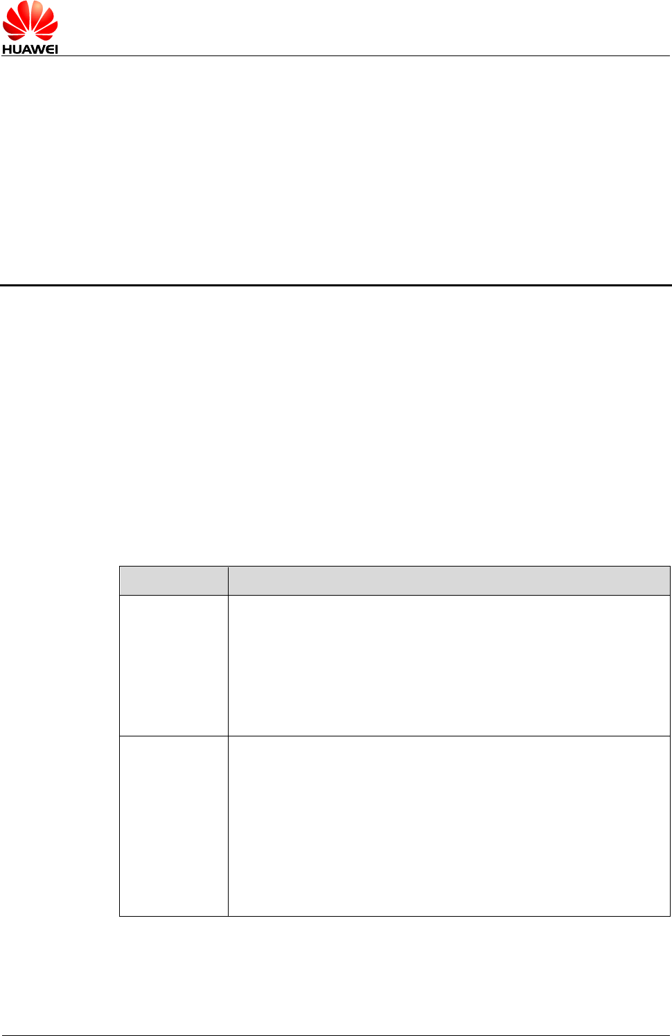
2.3 Circuit Block Diagram
The ME909s LGA module is developed based on Huawei's Balong Hi6921M platform.
Figure 2-1 shows the circuit block diagram of the module. The major functional units of
the module contain the following parts:
- Power Management
- Baseband Controller
HUAWEI ME909s Series LTE LGA Module
Hardware Guide
Overall Description
Issue 04 (2016-12-21)
Huawei Proprietary and Confidential
Copyright © Huawei Technologies Co., Ltd.
12
- Nand Flash
- RF Circuit
Figure 2-1 Circuit block diagram of the ME909s LGA module
Baseband Controller RFIC and Front end circuits
LGA Interface
VBAT
RESET
Power on/off
GPIO
GND
PCM
USB
UART
JTAG
WAKEUP_IN
USIM_Switch
USIM_DET
MAIN_ANT
AUX_ANT
LED
Nand flash
PMU
ADC
USIM
WAKEUP_OUT

HUAWEI ME909s Series LTE LGA Module
Hardware Guide
Description of the Application Interfaces
Issue 04 (2016-12-21)
Huawei Proprietary and Confidential
Copyright © Huawei Technologies Co., Ltd.
13
3 Description of the Application Interfaces
3.1 About This Chapter
This chapter mainly describes the external application interfaces of the ME909s LGA
module, including:
- LGA Interface
- Power Interface
- Signal Control Interface
- UART Interface
- USB Interface
- USIM Card Interface
- Audio Interface
- GPIO Interface
- ADC Interface
- JTAG Interface
- RF Antenna Interface
- Reserved Interface
- NC Interface
- Test Points Design
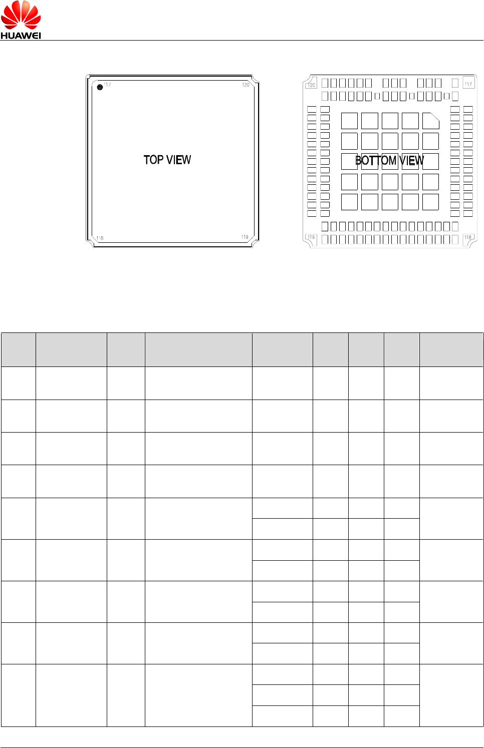
3.2 LGA Interface
The ME909s LGA module uses the 145-pin LGA as their external interface. For details
about the module and dimensions, see 6.4 Dimensions .
Figure 3-1 shows the sequence of pins on the 145-pin signal interface of the ME909s
LGA module.
HUAWEI ME909s Series LTE LGA Module
Hardware Guide
Description of the Application Interfaces
Issue 04 (2016-12-21)
Huawei Proprietary and Confidential
Copyright © Huawei Technologies Co., Ltd.
14
Figure 3-1 Sequence of LGA interface (Top view)
ADC
HUAWEI ME909s Series LTE LGA Module
Hardware Guide
Description of the Application Interfaces
Issue 04 (2016-12-21)
Huawei Proprietary and Confidential
Copyright © Huawei Technologies Co., Ltd.
15
Figure 3-2 Appearance of the module (Without Label)
Table 3-1 shows the definitions of pins on the 145-pin signal interface of the ME909s
LGA module.
Table 3-1 Definitions of pins on the LGA interface
Pin
No.
Pin Name
Pad
Type
Description
Parameter
Min.
(V)
Typ.
(V)
Max.
(V)
Comments
1
Reserved
-
Reserved, please keep
this pin open.
-
-
-
-
-
2
Reserved
-
Reserved, please keep
this pin open.
-
-
-
-
-
3
Reserved
-
Reserved, please keep
this pin open.
-
-
-
-
-
4
Reserved
-
Reserved, please keep
this pin open.
-
-
-
-
-
5
PCM_SYNC[1]
O
PCM sync
VOH
1.35
1.8
1.98
-
VOL
0
-
0.45
6
PCM_DIN
I
PCM data in
VIH
1.17
1.8
1.98
-
VIL
–0.3
-
0.63
7
PCM_DOUT
O
PCM data out
VOH
1.35
1.8
1.98
-
VOL
0
-
0.45
8
PCM_CLK[1]
O
PCM clock
VOH
1.35
1.8
1.98
-
VOL
0
-
0.45
9
SD_DATA1
I/O
SD Card data signal.
VOH
2.25
3.0
3.15
Only used
for
debugging.
Please
VOL
0
3.0
0.375
VIH
1.875
3.0
3.15
HUAWEI ME909s Series LTE LGA Module
Hardware Guide
Description of the Application Interfaces
Issue 04 (2016-12-21)
Huawei Proprietary and Confidential
Copyright © Huawei Technologies Co., Ltd.
16
Pin
No.
Pin Name
Pad
Type
Description
Parameter
Min.
(V)
Typ.
(V)
Max.
(V)
Comments
VIL
–0.3
3.0
0.721
5
reserve this
pin as the
test point.
10
SD_DATA2
I/O
SD Card data signal.
VOH
2.25
3.0
3.15
VOL
0
3.0
0.375
VIH
1.875
3.0
3.15
VIL
–0.3
3.0
0.721
5
11
WAKEUP_IN
I
Sleep authorization
signal.
H: Sleep mode is
disabled.
L: Sleep mode is
enabled (default value).
VIH
1.17
1.8
1.98
-
VIL
–0.3
-
0.63
12
VBAT
PI
Power supply input for
RF.
The rising time of VBAT
must be greater than
100 µs
-
3.2
3.8
4.2
-
13
VBAT
PI
Power supply input
The rising time of VBAT
must be greater than
100 µs
-
3.2
3.8
4.2
-
14
Reserved
I
Reserved, please keep
this pin open.
-
-
-
-
-
15
SLEEP_STAT
US
O
Sleep status indicator.
H: Module is in wakeup
state.
L: Module is in sleep
state.
VOH
1.35
1.8
1.98
-
VOL
0
-
0.45
16
Reserved
-
Reserved, please keep
this pin open.
-
-
-
-
-
17
Reserved
-
Reserved, please keep
this pin open.
-
-
-
-
-
18
Reserved
-
Reserved, please keep
this pin open.
-
-
-
-
-
19
Reserved
-
Reserved, please keep
this pin open.
-
-
-
-
-
20
Reserved
-
Reserved, please keep
this pin open.
-
-
-
-
-
HUAWEI ME909s Series LTE LGA Module
Hardware Guide
Description of the Application Interfaces
Issue 04 (2016-12-21)
Huawei Proprietary and Confidential
Copyright © Huawei Technologies Co., Ltd.
17
Pin
No.
Pin Name
Pad
Type
Description
Parameter
Min.
(V)
Typ.
(V)
Max.
(V)
Comments
21
Reserved
-
Reserved, please keep
this pin open.
-
-
-
-
-
22
Reserved
-
Reserved, please keep
this pin open.
-
-
-
-
-
23
Reserved
-
Reserved, please keep
this pin open.
-
-
-
-
-
24
Reserved
-
Reserved, please keep
this pin open.
-
-
-
-
-
25
NC
-
Not connected
-
-
-
-
-
26
NC
-
Not connected
-
-
-
-
-
27
Reserved
-
Reserved, please keep
this pin open.
-
-
-
-
-
28
UART2_TX
O
UART2 transmit output
VOH
1.35
1.8
1.98
Only used
for
debugging.
Please
reserve this
pin as the
test point.
VOL
0
-
0.45
29
UART2_RX
I
UART2 receive data
input
VIH
1.17
1.8
1.98
VIL
–0.3
-
0.63
30
JTAG_TMS
I
JTAG test mode select.
VIH
1.17
1.8
1.98
-
VIL
–0.3
-
0.63
31
Reserved
-
Reserved, please keep
this pin open.
-
-
-
-
-
32
VCC_EXT1
PO
1.8 V Power output
-
1.62
1.8
1.98
-
33
Reserved
-
Reserved, please keep
this pin open.
-
-
-
-
-
34
USIM_VCC
PO
Power supply for USIM
card.
-
1.75
1.8
1.98
USIM_VCC=
1.8 V
2.75
3.0
3.3
USIM_VCC=
3.0 V
35
Reserved
-
Reserved, please keep
this pin open.
-
-
-
-
-
36
JTAG_TRST_
N
I
JTAG reset
VIH
1.17
1.8
1.98
-
VIL
–0.3
-
0.63
37
Reserved
-
Reserved, please keep
this pin open.
-
-
-
-
-
38
NC
-
Not connected
-
-
-
-
-
HUAWEI ME909s Series LTE LGA Module
Hardware Guide
Description of the Application Interfaces
Issue 04 (2016-12-21)
Huawei Proprietary and Confidential
Copyright © Huawei Technologies Co., Ltd.
18
Pin
No.
Pin Name
Pad
Type
Description
Parameter
Min.
(V)
Typ.
(V)
Max.
(V)
Comments
39
NC
-
Not connected
-
-
-
-
-
40
NC
-
Not connected
-
-
-
-
-
41
NC
-
Not connected
-
-
-
-
-
42
JTAG_TCK
I
JTAG clock input
VIH
1.17
1.8
1.98
-
VIL
–0.3
-
0.63
43
GPIO1
I/O
General Purpose I/O
pins.
VOH
1.35
1.8
1.98
The function
of these pins
has not been
defined.
VOL
0
-
0.45
VIH
1.17
1.8
1.98
VIL
–0.3
-
0.63
44
Reserved
-
Reserved, please keep
this pin open.
-
-
-
-
-
45
Reserved
-
Reserved, please keep
this pin open.
-
-
-
-
-
46
GPIO2
I/O
General Purpose I/O
pins.
VOH
1.35
1.8
1.98
The function
of these pins
has not been
defined.
VOL
0
-
0.45
VIH
1.17
1.8
1.98
VIL
–0.3
-
0.63
47
NC
-
Not connected
-
-
-
-
-
48
GND
-
Ground
-
-
-
-
-
49
NOT USED
-
Do not design PAD
-
-
-
-
-
50
GND
-
Ground
-
-
-
-
-
51
GPIO3
I/O
General Purpose I/O
pins.
VOH
1.35
1.8
1.98
The function
of these pins
has not been
defined.
VOL
0
-
0.45
VIH
1.17
1.8
1.98
VIL
–0.3
-
0.63
52
GND
-
Ground
-
-
-
-
-
53
NOT USED
-
Do not design PAD
-
-
-
-
-
54
GND
-
Ground
-
-
-
-
-
55
GPIO4/USIM_
Switch
I/O
General Purpose I/O
pins (Default) or USIM
VOH
1.35
1.8
1.98
The function
of this pin
can be used
HUAWEI ME909s Series LTE LGA Module
Hardware Guide
Description of the Application Interfaces
Issue 04 (2016-12-21)
Huawei Proprietary and Confidential
Copyright © Huawei Technologies Co., Ltd.
19
Pin
No.
Pin Name
Pad
Type
Description
Parameter
Min.
(V)
Typ.
(V)
Max.
(V)
Comments
Switch control signal.
VOL
0
-
0.45
as GPIO or
USIM
Switch, while
the USIM
Switch
should be
enabled by
AT
command.
VIH
1.17
1.8
1.98
VIL
–0.3
-
0.63
56
GND
-
Ground
-
-
-
-
-
57
NOT USED
-
Do not design PAD
-
-
-
-
-
58
GND
-
Ground
-
-
-
-
-
59
GND
-
Ground
-
-
-
-
-
60
Reserved
-
Reserved, please keep
this pin open.
-
-
-
-
-
61
Reserved
-
Reserved, please keep
this pin open.
-
-
-
-
-
62
Reserved
-
Reserved, please keep
this pin open.
-
-
-
-
-
63
Reserved
-
Reserved, please keep
this pin open.
-
-
-
-
-
64
Reserved
-
Reserved, please keep
this pin open.
-
-
-
-
-
65
Reserved
-
Reserved, please keep
this pin open.
-
-
-
-
-
66
SD_DATA3
I/O
SD Card data signal.
VOH
2.25
3.0
3.15
Only used
for
debugging.
Please
reserve this
pin as the
test point.
VOL
0
3.0
0.375
VIH
1.875
3.0
3.15
VIL
–0.3
3.0
0.721
5
67
SD_CLK
O
SD Card CLK signal.
VOH
2.25
3.00
3.15
VOL
0
-
0.375
68
SD_DATA0
I/O
SD Card data signal.
VOH
2.25
3.0
3.15
VOL
0
3.0
0.375
VIH
1.875
3.0
3.15
HUAWEI ME909s Series LTE LGA Module
Hardware Guide
Description of the Application Interfaces
Issue 04 (2016-12-21)
Huawei Proprietary and Confidential
Copyright © Huawei Technologies Co., Ltd.
20
Pin
No.
Pin Name
Pad
Type
Description
Parameter
Min.
(V)
Typ.
(V)
Max.
(V)
Comments
VIL
–0.3
3.0
0.721
5
69
SD_CMD
O
SD Card cmd signal.
VOH
2.25
3.00
3.15
VOL
0
-
0.375
70
USIM_DET
I
USIM hot swap
detection pin.
When it is High, USIM is
present.
When it is Low, USIM is
absent.
VIH
1.62
1.8
1.98
The signal is
internally
pulled up.
Keep
USIM_DET
floating, if it
is not used.
VIL
0
-
0.18
71
WAKEUP_OU
T
O
Module to wake up the
host.
VOH
1.35
1.8
1.98
-
VOL
0
-
0.45
72
JTAG_TDO
O
JTAG test data output
VOH
1.35
1.8
1.98
-
VOL
0
-
0.45
73
UART0_DSR
O
UART0 data set Ready
VOH
1.35
1.8
1.98
-
VOL
0
-
0.45
74
UART0_RTS
O
UART0 request to send
VOH
1.35
1.8
1.98
-
VOL
0
-
0.45
75
UART0_DCD
O
UART0 Data Carrier
Detect
VOH
1.35
1.8
1.98
-
VOL
0
-
0.45
76
UART0_TX
O
UART0 transmit output
VOH
1.35
1.8
1.98
-
VOL
0
-
0.45
77
UART0_RING
O
UART0 Ring Indicator
VOH
1.35
1.8
1.98
-
VOL
0
-
0.45
78
UART0_RX
I
UART0 receive data
input
VIH
1.17
1.8
1.98
-
VIL
–0.3
-
0.63
79
UART0_DTR
I
UART0 Data Terminal
Ready
VIH
1.17
1.8
1.98
-
VIL
–0.3
-
0.63
80
UART0_CTS
I
UART0 Clear to Send
VIH
1.17
1.8
1.98
-
VIL
–0.3
-
0.63
81
POWER_ON_
OFF
I
System power-on or
power-off
VIH
1.62
1.8
1.98
The signal is
internally
pulled up.
VIL
0
-
0.18
HUAWEI ME909s Series LTE LGA Module
Hardware Guide
Description of the Application Interfaces
Issue 04 (2016-12-21)
Huawei Proprietary and Confidential
Copyright © Huawei Technologies Co., Ltd.
21
Pin
No.
Pin Name
Pad
Type
Description
Parameter
Min.
(V)
Typ.
(V)
Max.
(V)
Comments
82
NC
-
Not connected
-
-
-
-
-
83
NC
-
Not connected
-
-
-
-
-
84
NC
-
Not connected
-
-
-
-
-
85
USB_DM
I/O
USB Data- defined in
the USB 2.0
Specification
-
-
-
-
-
86
USB_DP
I/O
USB Data+ defined in
the USB 2.0
Specification.
-
-
-
-
-
87
JTAG_TDI
I
JTAG test data input
VIH
1.17
1.8
1.98
-
VIL
–0.3
-
0.63
88
USIM_RESET
O
USIM card reset
VOH
0.7x
USIM
_VCC
-
3.3
USIM_VCC=
1.8 V or 3.0
V
VOL
0
-
0.2x
USIM
_VCC
89
USIM_DATA
I/O
USIM card data
VOH
0.7 x
USIM
_VCC
-
3.3
USIM_VCC=
1.8 V or 3.0
V
VOL
0
-
0.2 x
USIM
_VCC
VIH
0.65x
USIM
_VCC
-
3.30
VIL
0
-
0.25x
USIM
_VCC
90
USIM_CLK
O
USIM card clock
VOH
0.7 x
USIM
_VCC
-
3.3
USIM_VCC=
1.8 V or 3.0
V
VOL
0
-
0.2 x
USIM
_VCC
91
Reserved
-
Reserved, please keep
this pin open.
-
-
-
-
-
92
SD_VCC
PO
SD Card power signal.
-
2.85
3.00
3.15
-
93
JTAG_RTCK
O
JTAG return clock, Pin
VOH
1.35
1.8
2.1
-
HUAWEI ME909s Series LTE LGA Module
Hardware Guide
Description of the Application Interfaces
Issue 04 (2016-12-21)
Huawei Proprietary and Confidential
Copyright © Huawei Technologies Co., Ltd.
22
Pin
No.
Pin Name
Pad
Type
Description
Parameter
Min.
(V)
Typ.
(V)
Max.
(V)
Comments
for trace connection, it
is a reserved test point
for customers.
VOL
0
-
0.45
94
Reserved
-
Reserved, please keep
this pin open.
-
-
-
-
-
95
Reserved
-
Reserved, please keep
this pin open.
-
-
-
-
-
96
Reserved
-
Reserved, please keep
this pin open.
-
-
-
-
-
97
Reserved
-
Reserved, please keep
this pin open.
-
-
-
-
-
98
Reserved
-
Reserved, please keep
this pin open.
-
-
-
-
-
99
Reserved
-
Reserved, please keep
this pin open.
-
-
-
-
-
100
RESIN_N
I
Reset module.
VIH
1.62
1.8
1.98
The signal is
internally
pulled up.
VIL
0
-
0.18
101
LED_MODE
O
Mode indicator
current sink
Drive strength: 10 mA
-
-
-
-
102
ADC_1
AI
Conversion interface for
analog signals to digital
signals
-
0
-
2.5
-
103
Reserved
-
Reserved, please keep
this pin open.
-
-
-
-
-
104
ADC_2
AI
Conversion interface for
analog signals to digital
signals
-
0
-
2.5
-
105
GPIO5
I/O
General Purpose I/O
pins.
VOH
1.35
1.8
1.98
The function
of these pins
has not been
defined.
VOL
0
-
0.45
VIH
1.17
1.8
1.98
VIL
–0.3
-
0.63
106
GND
-
Ground
-
-
-
-
-
107
MAIN_ANT
-
RF main antenna pad
-
-
-
-
-
108
GND
-
Ground
-
-
-
-
-
109
GPIO6
I/O
General Purpose I/O
VOH
1.35
1.8
1.98
The function
HUAWEI ME909s Series LTE LGA Module
Hardware Guide
Description of the Application Interfaces
Issue 04 (2016-12-21)
Huawei Proprietary and Confidential
Copyright © Huawei Technologies Co., Ltd.
23
Pin
No.
Pin Name
Pad
Type
Description
Parameter
Min.
(V)
Typ.
(V)
Max.
(V)
Comments
pins.
VOL
0
-
0.45
of these pins
has not been
defined.
VIH
1.17
1.8
1.98
VIL
–0.3
-
0.63
110
GND
-
Ground
-
-
-
-
-
111
NC
-
Not connected
-
-
-
-
-
112
GND
-
Ground
-
-
-
-
-
113
GPIO7
I/O
General Purpose I/O
pins
VOH
1.35
1.8
1.98
The function
of these pins
has not been
defined.
VOL
0
-
0.45
VIH
1.17
1.8
1.98
VIL
–0.3
-
0.63
114
GND
-
Ground
-
-
-
-
-
115
AUX_ANT
-
RF AUX antenna pad
-
-
-
-
-
116
GND
-
Ground
-
-
-
-
-
117
NC
-
Not connected
-
-
-
-
-
118
NC
-
Not connected
-
-
-
-
-
119
NC
-
Not connected
-
-
-
-
-
120
NC
-
Not connected
-
-
-
-
-
121
GND
-
Thermal Ground Pad
-
-
-
-
-
122
GND
-
Thermal Ground Pad
-
-
-
-
-
123
GND
-
Thermal Ground Pad
-
-
-
-
-
124
GND
-
Thermal Ground Pad
-
-
-
-
-
125
GND
-
Thermal Ground Pad
-
-
-
-
-
126
GND
-
Thermal Ground Pad
-
-
-
-
-
127
GND
-
Thermal Ground Pad
-
-
-
-
-
128
GND
-
Thermal Ground Pad
-
-
-
-
-
129
GND
-
Thermal Ground Pad
-
-
-
-
-
130
GND
-
Thermal Ground Pad
-
-
-
-
-
131
GND
-
Thermal Ground Pad
-
-
-
-
-
132
GND
-
Thermal Ground Pad
-
-
-
-
-
133
GND
-
Thermal Ground Pad
-
-
-
-
-
HUAWEI ME909s Series LTE LGA Module
Hardware Guide
Description of the Application Interfaces
Issue 04 (2016-12-21)
Huawei Proprietary and Confidential
Copyright © Huawei Technologies Co., Ltd.
24
Pin
No.
Pin Name
Pad
Type
Description
Parameter
Min.
(V)
Typ.
(V)
Max.
(V)
Comments
134
GND
-
Thermal Ground Pad
-
-
-
-
-
135
GND
-
Thermal Ground Pad
-
-
-
-
-
136
GND
-
Thermal Ground Pad
-
-
-
-
-
137
GND
-
Thermal Ground Pad
-
-
-
-
-
138
GND
-
Thermal Ground Pad
-
-
-
-
-
139
GND
-
Thermal Ground Pad
-
-
-
-
-
140
GND
-
Thermal Ground Pad
-
-
-
-
-
141
GND
-
Thermal Ground Pad
-
-
-
-
-
142
GND
-
Thermal Ground Pad
-
-
-
-
-
143
GND
-
Thermal Ground Pad
-
-
-
-
-
144
GND
-
Thermal Ground Pad
-
-
-
-
-
145
GND
-
Thermal Ground Pad
-
-
-
-
-
- P indicates power pins; PI indicates input power pins; PO indicates output power pins; I
indicates pins for digital signal input; O indicates pins for digital signal output; AI indicates
pins for analog signal input.
- VIL indicates Low-level Input voltage; VIH indicates High-level Input voltage; VOL indicates
Low-level Output voltage; VOH indicates High-level Output voltage.
- The NC (Not Connected) pins are floating and there are no signal connected to these pins.
- The Reserved pins are internally connected to the module. Therefore, these pins should not
be used, otherwise they may cause problems. Please contact with us for more details about
this information.
- [1]: PCM_SYNC and PCM_CLK: Output, when ME909s LGA module is used as PCM
master.
3.3 Power Interface
3.3.1 Overview
The power supply part of the ME909s LGA module contains:
- VBAT pins for the power supply
- VCC_EXT1 pin for external power output with 1.8 V
- USIM_VCC pin for USIM card power output
- SD_VCC pin for SD card power output
Table 3-2 lists the definitions of the pins on the power supply interface.
HUAWEI ME909s Series LTE LGA Module
Hardware Guide
Description of the Application Interfaces
Issue 04 (2016-12-21)
Huawei Proprietary and Confidential
Copyright © Huawei Technologies Co., Ltd.
25
Table 3-2 Definitions of the pins on the power supply interface
Pin No.
Pin
Name
Pad
Type
Description
Parameter
Min.
(V)
Typ.
(V)
Max.
(V)
Comments
12 and 13
VBAT
PI
Power supply input for
RF.
The rising time of
VBAT must be greater
than 100 µs
-
3.2
3.8
4.2
-
32
VCC_EXT1
PO
1.8 V Power output
-
1.62
1.8
1.98
-
34
USIM_VCC
PO
Power supply for
USIM card
-
1.75
1.8
1.98
USIM_VCC=
1.8 V
2.75
3.0
3.3
USIM_VCC=
3.0 V
92
SD_VCC
PO
SD Card Power.
-
2.85
3.00
3.15
-
48, 50, 52,
54, 56, 58,
59, 106,
108, 110,
112, 114
and 116
GND
-
GND
-
-
-
-
-
121–145
GND
-
Thermal Ground Pad
-
-
-
-
-
3.3.2 Power Supply VBAT Interface
When the ME909s LGA module works normally, power is supplied through the VBAT
pins and the voltage ranges from 3.2 V to 4.2 V (typical value: 3.8 V). The 145-pin
LGA provides two VBAT pins and GND pins for external power input. To ensure that
the ME909s LGA module works normally, all the pins must be used efficiently.
When the ME909s LGA module is used for different external applications, pay special
attention to the design for the power supply. When the ME909s LGA module works at
2G mode and transmits signals at the maximum power, the transient current may
reach the transient peak value of about 2.75 A due to the differences in actual network
environments. In this case, the VBAT voltage drops. If you want wireless good
performance, please make sure that the voltage does not decrease below 3.2 V in any
case. Otherwise, exceptions such as restart of the ME909s LGA module may occur.
A low-dropout (LDO) regulator or switch power with current output of more than 3 A is
recommended for external power supply. Furthermore, five 220 µF or above energy
storage capacitors are connected in parallel at the power interface of the ME909s LGA
module. In addition, to reduce the impact of channel impedance on voltage drop, you
are recommended to try to shorten the power supply circuit of the VBAT interface.
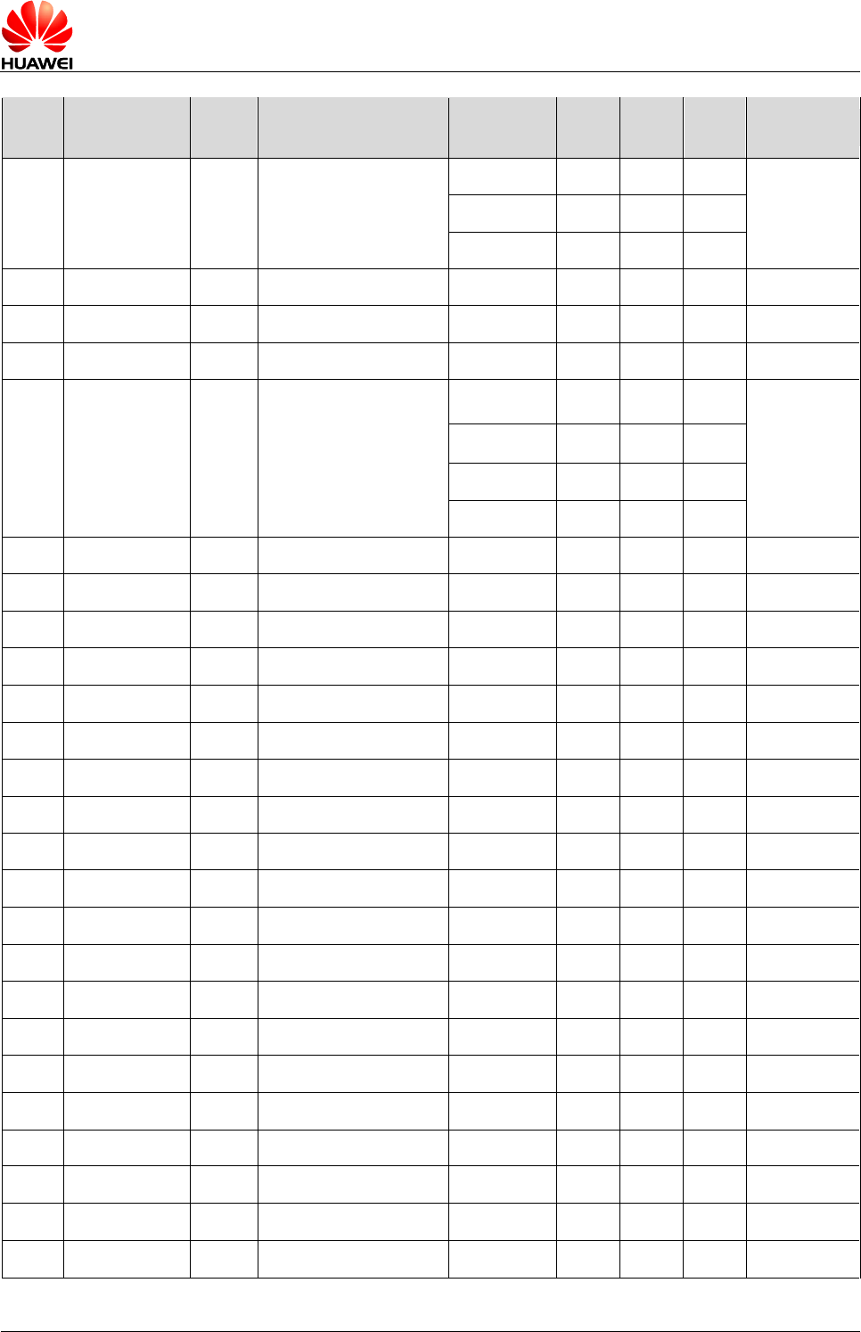
It is recommended that customers add the EMI ferrite bead (FBMJ1608HS280NT
manufactured by TAIYO YUDEN or MPZ1608S300ATAH0 manufactured by TDK is
recommended) to directly isolate DTE from DCE in the power circuit. Figure 3-3
shows the recommended power circuit of ME909s LGA module.
HUAWEI ME909s Series LTE LGA Module
Hardware Guide
Description of the Application Interfaces
Issue 04 (2016-12-21)
Huawei Proprietary and Confidential
Copyright © Huawei Technologies Co., Ltd.
26
Figure 3-3 Recommended power circuit of ME909s LGA module
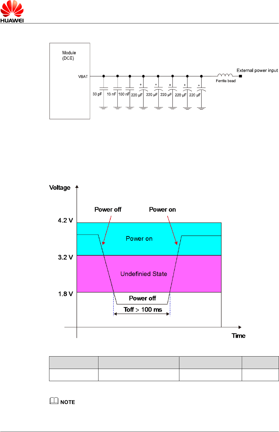
When the system power restarts, a discharge circuit is recommended to make sure
the power voltage drops below 1.8 V and stays for 100 ms at least. If
POWER_ON_OFF is asserted when the VBAT ranges from 1.8 V to 3.2 V, the module
may enter an unexpected status.
Figure 3-4 Power supply time sequence for power cycling
Parameter
Remarks
Time (Min.)
Unit
Toff
Power off time
100
ms
The rising time of VBAT should be 100 µs at least.
HUAWEI ME909s Series LTE LGA Module
Hardware Guide
Description of the Application Interfaces
Issue 04 (2016-12-21)
Huawei Proprietary and Confidential
Copyright © Huawei Technologies Co., Ltd.
27
3.3.3 Output Power Supply Interface
Output power supply interfaces are VCC_EXT, USIM_VCC and SD_VCC.
Through the VCC_EXT, the module can supply 1.8 V power externally with an output
current of 10 mA (typical value) for external level conversion or other applications. If
the module is in power down mode, the output power supply is in the disabled state.
Through the USIM_VCC, the module can supply 1.8 V or 3.0 V power to the USIM
card.
The SD_VCC is SD card power that only used for debugging. Please reserve the test
point.
3.4 Signal Control Interface
3.4.1 Overview
The signal control part of the interface on the ME909s LGA module consists of the
following:
- Power-on/off (POWER_ON_OFF) pin
- System reset (RESIN_N) pin
- WAKEUP_IN signal (WAKEUP_IN) pin
- WAKEUP_OUT signal (WAKEUP_OUT) pin
- SLEEP_STATUS signal (SLEEP_STATUS) pin
- LED signal (LED_MODE) pin
- USIM_DET signal (USIM_DET) pin
Table 3-3 lists the pins on the signal control interface.
Table 3-3 Definitions of the pins on the signal control interface
Pin
No.
Pin Name
Pad
Type
Description
Parameter
Min.
(V)
Typ.
(V)
Max.
(V)
Comments
81
POWER_ON_OFF
I
System power-on
and power-off
VIH
1.62
1.8
1.98
The signal is
internally
pulled up.
VIL
0
-
0.18
100
RESIN_N
I
Reset module.
VIH
1.62
1.8
1.98
The signal is
internally
pulled up。
VIL
0
-
0.18
11
WAKEUP_IN[1]
I
Sleep authorization
signal
H: Sleep mode is
disabled
L: Sleep mode is
enabled (default
value)
VIH
1.17
1.8
1.98
-
VIL
–0.3
-
0.63
HUAWEI ME909s Series LTE LGA Module
Hardware Guide
Description of the Application Interfaces
Issue 04 (2016-12-21)
Huawei Proprietary and Confidential
Copyright © Huawei Technologies Co., Ltd.
28
Pin
No.
Pin Name
Pad
Type
Description
Parameter
Min.
(V)
Typ.
(V)
Max.
(V)
Comments
71
WAKEUP_OUT[2]
O
Module to wake up
the host.
H: Wake up the
host, the module
hold 1s
high-level-voltage
pulse and then
output
low-level-voltage
L: Do not wake up
the host (default
value)
VOH
1.35
1.8
1.98
-
VOL
0
-
0.45
15
SLEEP_STATUS[3]
O
Sleep status
indicator
H: Module is in
wake state
L: Module is in
sleep state
VOH
1.35
1.8
1.98
-
VOL
0
-
0.45
-
101
LED_MODE
O
Mode indicator
current sink Drive
strength: 10 mA
-
-
-
-
-
70
USIM_DET
I
USIM hot swap
detection pin.
When it is High,
USIM is present.
When it is Low,
USIM is absent.
VIH
1.62
1.8
1.98
The signal is
internally
pulled up.
Keep
USIM_DET
floating, if it
is not used.
VIL
0
-
0.18
- [1]: The WAKEUP_IN pin can be used to wake up the module.
- [2]: WAKEUP_OUT: When the module is not in sleep mode, this pin's drive current is 4 mA.
When the module is in sleep mode, this pin's output level is low and drive current
smaller than 0.1 mA. The resistance is maintained at 5 kΩ–15 kΩ, as shown in Figure
3-5 . The output level may be changed if there is a stronger pull-up. It is
recommended that customers take Figure 3-12 for reference to design their circuit.
- [3]: SLEEP_STATUS: When the module is not in sleep mode, this pin's drive current is 4
mA.
When the module is in sleep mode, this pin's output level is low and drive current
smaller than 0.1 mA. The resistance is maintained at 5 kΩ–15 kΩ, as shown in Figure
3-5 . The output level may be changed if there is a stronger pull-up. It is
recommended that customers take Figure 3-13 for reference to design their circuit.
HUAWEI ME909s Series LTE LGA Module
Hardware Guide
Description of the Application Interfaces
Issue 04 (2016-12-21)
Huawei Proprietary and Confidential
Copyright © Huawei Technologies Co., Ltd.
29
Figure 3-5 Maintaining the resistance in sleep mode
BB Chip
Module
(Modem)
R=5–15 K
3.4.2 Power-on/off Pin
The ME909s LGA module can be controlled to power on/off by the POWER_ON_OFF
pin.
Table 3-4 Two states of POWER_ON_OFF
Item
Pin state
Description
1
Low (when ME909s
LGA module is in
power off state.)
ME909s LGA module is powered on.
POWER_ON_OFF pin should be pulled down for
1.0s at least.
2
Low (when ME909s
LGA module is in
power on state.)
ME909s LGA module is powered off.
POWER_ON_OFF pin should be pulled down for
4.0s at least.
HUAWEI ME909s Series LTE LGA Module
Hardware Guide
Description of the Application Interfaces
Issue 04 (2016-12-21)
Huawei Proprietary and Confidential
Copyright © Huawei Technologies Co., Ltd.
30
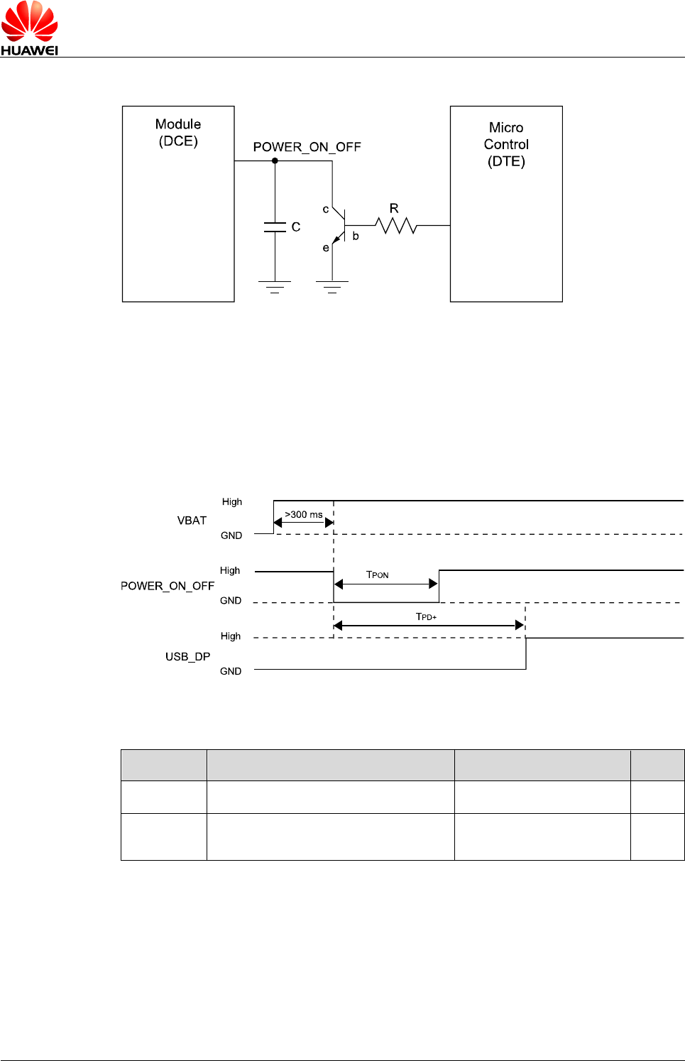
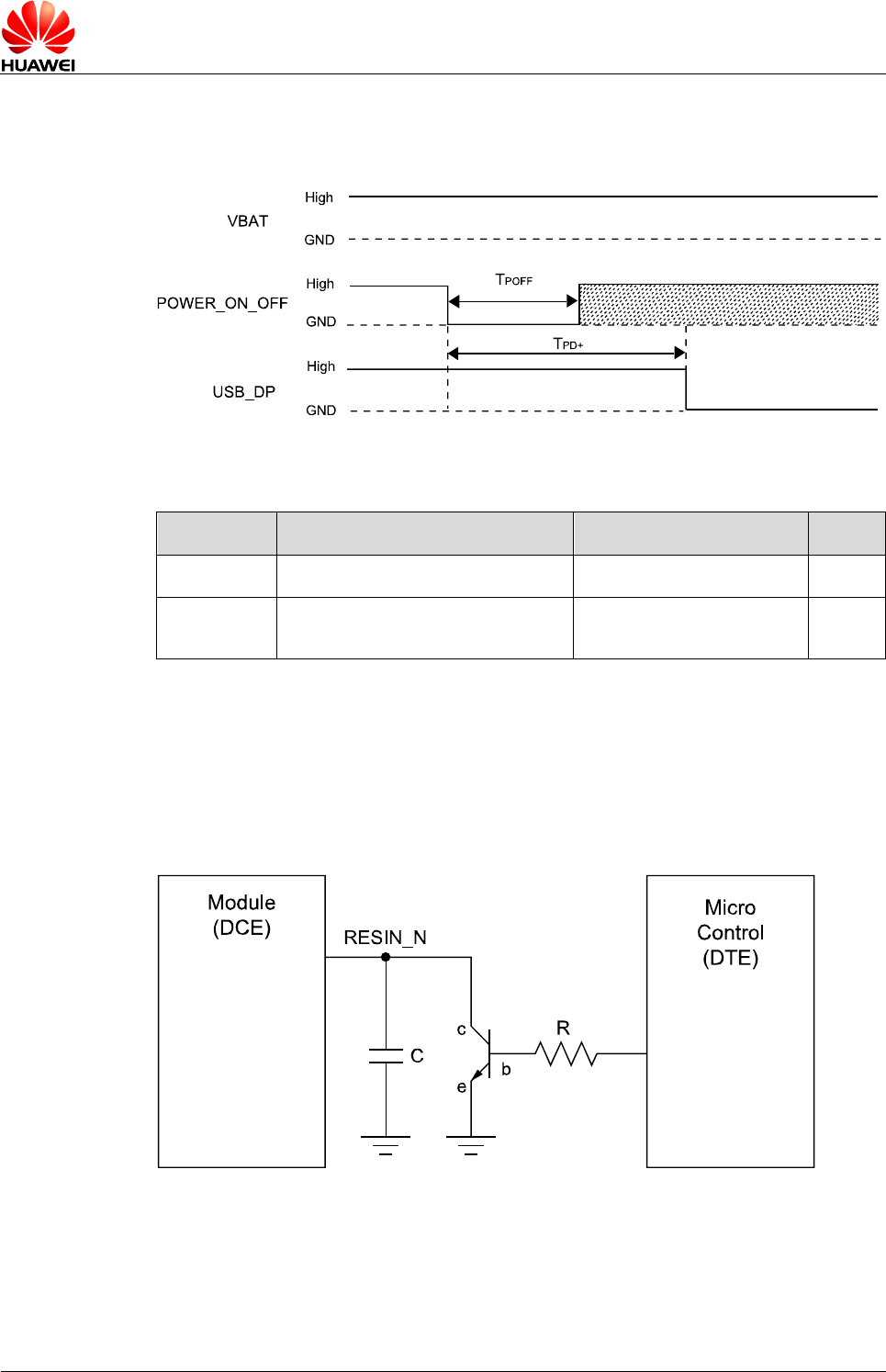
Figure 3-6 Connections of the POWER_ON_OFF pin
Power-On Time Sequence
After VBAT has been applied and is stable, the POWER_ON_OFF signal is pulled
down, and then the module will boot up.
During power on timing, please make sure the VBAT is stable.
Figure 3-7 Power on timing sequence
Table 3-5 Power on timing
Parameter
Comments
Time (Nominal values)
Units
TPON
POWER_ON_OFF turn on time.
> 1.0
s
TPD+
POWER_ON_OFF valid to USB
D+ high
About 7.0
s
If the DTE needs to detect the PID/VID of module during the BIOS phase, the
detection time should exceed the TPD+ time.
HUAWEI ME909s Series LTE LGA Module
Hardware Guide
Description of the Application Interfaces
Issue 04 (2016-12-21)
Huawei Proprietary and Confidential
Copyright © Huawei Technologies Co., Ltd.
31
Power-Off Time Sequence
Figure 3-8 Power off timing sequence
Table 3-6 Power off timing
Parameter
Comments
Time (Nominal values)
Units
TPOFF
POWER_ON_OFF turn off time.
> 4.0
s
TPD+
POWER_ON_OFF valid to USB
D+ low
> 4.0
s
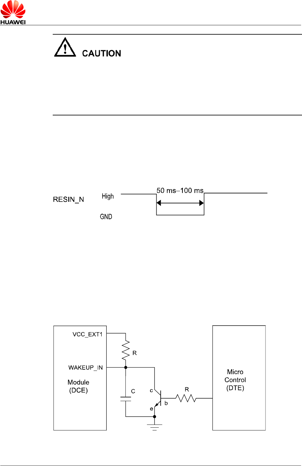
3.4.3 RESIN_N
The RESIN_N pin is used to reset the module's system. When the software stops
responding, the RESIN_N pin can be pulled down to reset the hardware.
Figure 3-9 Connections of the RESIN_N pin
HUAWEI ME909s Series LTE LGA Module
Hardware Guide
Description of the Application Interfaces
Issue 04 (2016-12-21)
Huawei Proprietary and Confidential
Copyright © Huawei Technologies Co., Ltd.
32
As the RESIN_N and POWER_ON_OFF signals are relatively sensitive, it is
recommended that you install a 10 nF–0.1 µF capacitor near the RESIN_N and
POWER_ON_OFF pins of the interface for filtering. In addition, when you design a
circuit on the PCB of the interface board, it is recommended that the circuit length not
exceed 20 mm and that the circuit be kept at a distance of 2.54 mm (100 mil) at least
from the PCB edge. Furthermore, you need to wrap the area adjacent to the signal
wire with a ground wire. Otherwise, the module may be reset due to interference.
The ME909s LGA module supports hardware reset function. If the software of the
ME909s LGA module stops responding, you can reset the hardware through the
RESIN_N signal as shown in Figure 3-10 .When a low-level pulse is supplied through
the RESIN_N pin, the hardware will be reset. After the hardware is reset, the software
starts powering on the module and reports relevant information according to the actual
settings. For example, the AT command automatically reports ^SYSSTART.
Figure 3-10 Reset pulse timing
3.4.4 WAKEUP_IN Signal
WAKEUP_IN pin is the authorization signal of ME909s LGA module entering sleep
mode. If this pin is not connected, it will keep in low level by default.
Table 3-3 shows the definition of the WAKEUP_IN signal.
The module cannot enter sleep mode when this pin is pulled up (1.8 V), and the
module should be waked up when the pin is pulled up.
Figure 3-11 Connections of the WAKEUP_IN pin
HUAWEI ME909s Series LTE LGA Module
Hardware Guide
Description of the Application Interfaces
Issue 04 (2016-12-21)
Huawei Proprietary and Confidential
Copyright © Huawei Technologies Co., Ltd.
33
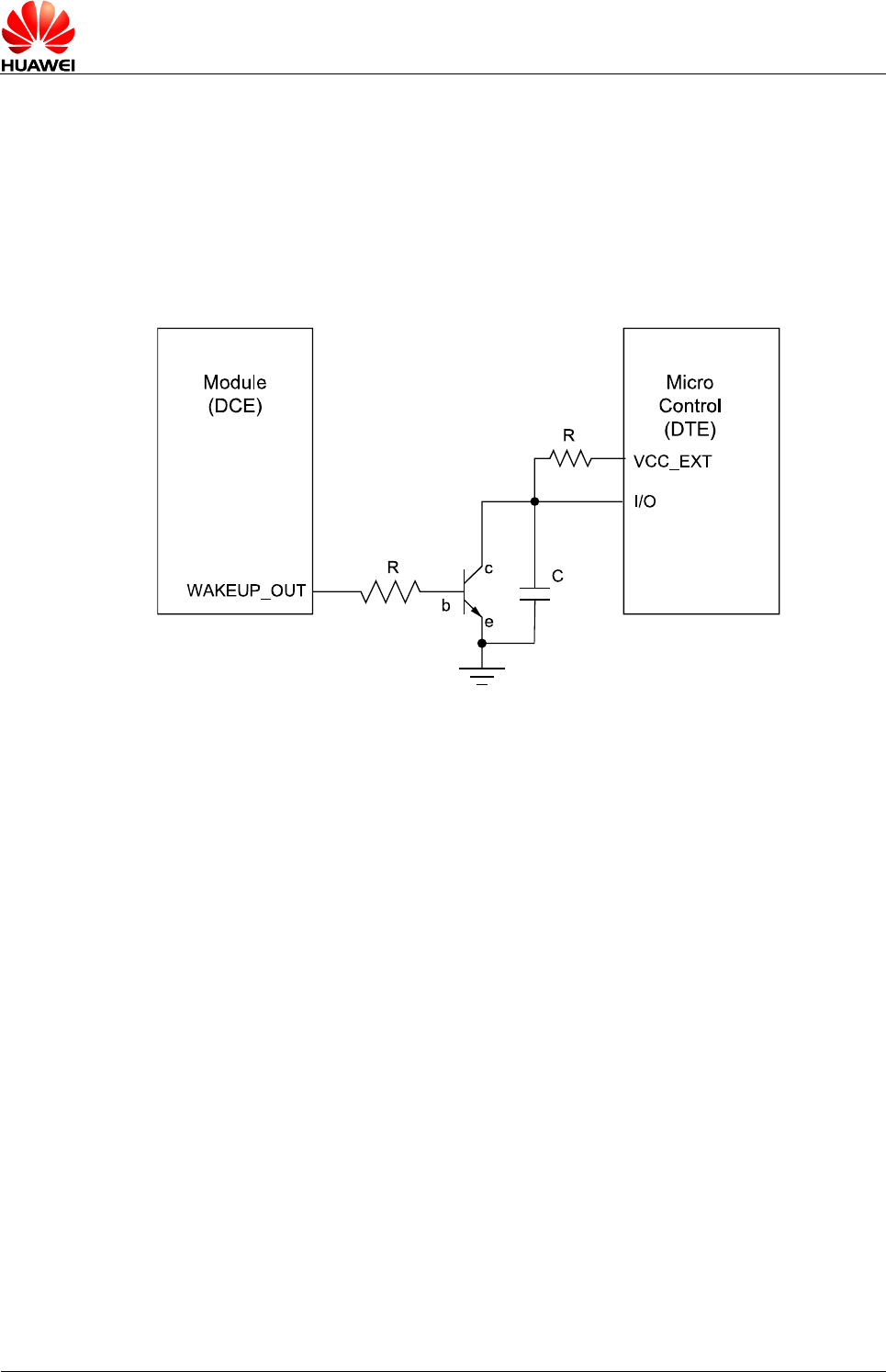
3.4.5 WAKEUP_OUT Signal
The WAKEUP_OUT pin is used to wake up the external devices.
- When WAKEUP_OUT pin is in high level, the module can wake up the host.
- When WAKEUP_OUT pin is in low level, the module cannot wake up the host.
(default)
Figure 3-12 Connections of the WAKEUP_OUT pin
3.4.6 SLEEP_STATUS Signal
The SLEEP_STATUS pin is used to indicate the sleep status of the module.
- When SLEEP_STATUS pin is in high level, the module is in wakeup state.
- When SLEEP_STATUS pin is in low level, the module is in sleep state.

HUAWEI ME909s Series LTE LGA Module
Hardware Guide
Description of the Application Interfaces
Issue 04 (2016-12-21)
Huawei Proprietary and Confidential
Copyright © Huawei Technologies Co., Ltd.
34
Figure 3-13 Connections of the SLEEP_STATUS pin
3.4.7 LED_MODE Signal
ME909s LGA module provides an LED_MODE signal to indicate the work status.
Table 3-7 State of the LED_MODE pin
No.
Operating Status
LED_MODE
1
No service/Restricted service
Outputs: low (0.1s)-high (0.1s)-low
(0.1s)-high (1.7s)
2s cycle
2
Register to the network
Outputs: low (0.1s)-high (1.9s)
2s cycle
3
Dial-up successfully
Outputs: low
Figure 3-14 shows the recommended circuits of LED_MODE. The brightness of LED
can be adjusted by adjusting the resistance of the resistor.

HUAWEI ME909s Series LTE LGA Module
Hardware Guide
Description of the Application Interfaces
Issue 04 (2016-12-21)
Huawei Proprietary and Confidential
Copyright © Huawei Technologies Co., Ltd.
35
Figure 3-14 Driving circuit
LED_MODE
Module
(DCE)
R
VBAT
3.4.8 USIM_DET Pin
ME909s LGA module supports USIM hot swap function.
ME909s LGA module provides an input pin (USIM_DET) to detect whether the USIM
card is present or not. This pin is a level trigger pin, and it is internally pulled up. If the
module does not support USIM card hot swap, keep USIM_DET floating.
Table 3-8 Function of the USIM_DET pin
No.
USIM_DET
Function
1
High level
USIM card insertion.
If the USIM card is present, USIM_DET should be High.
2
Low level
USIM card removal.
If the USIM card is absent, USIM_DET should be Low.
HUAWEI ME909s Series LTE LGA Module
Hardware Guide
Description of the Application Interfaces
Issue 04 (2016-12-21)
Huawei Proprietary and Confidential
Copyright © Huawei Technologies Co., Ltd.
36
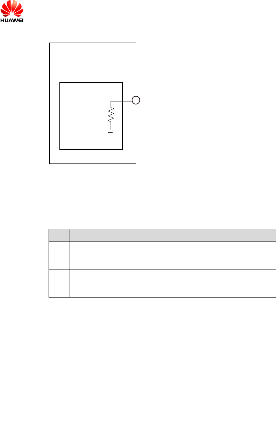
Figure 3-15 Connections of the USIM_DET pin
Module
(DCE) 1.8 V
USIM_DET
USIM Deck
470 pF
CD
1 kΩ
BB Chip
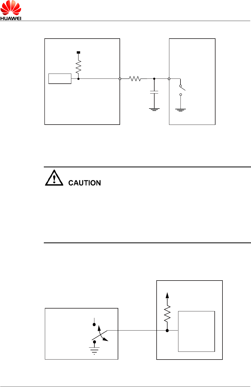
CD is a pin detecting of USIM in the USIM socket, in normal, there will be a detect pin
in the USIM socket.
- It is recommended not to add a diode on the USIM_DET pin outside the module.
- The normal SHORT USIM connector should be employed. The logic of USIM_DET
is shown as Figure 3-16 . High represents that USIM is inserted; Low represents
that USIM is removed.
- When USIM is inserted (hot), USIM_DET will change from Low to High;
- When USIM is removed (hot), USIM_DET will change from High to Low;
- The module will detect the level of USIM_DET to support the hot swap.
Figure 3-16 Logic of USIM_DET
Modem
Processor
USIM Connector Switch
USIM installed=
Not Connected
USIM not
installed=
GND
WWAN Module
USIM_DET
1.8V
HUAWEI ME909s Series LTE LGA Module
Hardware Guide
Description of the Application Interfaces
Issue 04 (2016-12-21)
Huawei Proprietary and Confidential
Copyright © Huawei Technologies Co., Ltd.
37
3.5 UART Interface
3.5.1 Overview
The ME909s LGA module provides the UART0 (8-wire UART) interface for one
asynchronous communication channel. As the UART0 interface supports signal
control through standard modem handshake, AT commands are entered and serial
communication is performed through the UART0 interface. The UART2 (2-wire UART)
interface is provided for only debugging by the ME909s LGA module. The UART have
the following features:
- Full-duplex
- 7-bit or 8-bit data
- 1-bit or 2-bit stop bit
- Odd parity check, even parity check, or non-check
- Baud rate clock generated by the system clock
- Direct memory access (DMA) transmission
- UART0 supports baud rate: 300 bit/s, 600 bit/s, 1200 bit/s, 2400 bit/s ,4800 bit/s,
9600 bit/s, 19200 bit/s, 38400 bit/s, 57600 bit/s, 115200 bit/s (default), 230400
bit/s, 1000000 bit/s, 3000000 bit/s
- Baud rate auto adaptive change is supported. AP (Access Point) must choose
one default Baud rate to communicate with module in the beginning.
The 2-wire UART is for debugging only. Customers should layout two test points for
them, which are required for system troubleshooting and analysis.
Table 3-9 UART interface signals
Pin
No.
Pin Name
Pad
Type
Description
Parameter
Min.
(V)
Typ.
(V)
Max.
(V)
Comments
76
UART0_TX
O
UART0 transmit output
VOH
1.35
1.8
1.98
-
VOL
0
-
0.45
-
78
UART0_RX
I
UART0 receive data
input
VIH
1.17
1.8
1.98
-
VIL
–0.3
-
0.63
-
77
UART0_RING
O
UART0 ring indicator
VOH
1.35
1.8
1.98
-
VOL
0
-
0.45
-
74
UART0_RTS
O
UART0 request to send
VOH
1.35
1.8
1.98
-
VOL
0
-
0.45
-
79
UART0_DTR
I
UART0 data terminal
ready
VIH
1.17
1.8
1.98
-
VIL
–0.3
-
0.63
-
80
UART0_CTS
I
UART0 clear to send
VIH
1.17
1.8
1.98
-
VIL
–0.3
-
0.63
-
75
UART0_DCD
O
UART0 data carrier
VOH
1.35
1.8
1.98
-
HUAWEI ME909s Series LTE LGA Module
Hardware Guide
Description of the Application Interfaces
Issue 04 (2016-12-21)
Huawei Proprietary and Confidential
Copyright © Huawei Technologies Co., Ltd.
38
Pin
No.
Pin Name
Pad
Type
Description
Parameter
Min.
(V)
Typ.
(V)
Max.
(V)
Comments
detect
VOL
0
-
0.45
-
73
UART0_DSR
O
UART0 data set ready
VOH
1.35
1.8
1.98
-
VOL
0
-
0.45
-
28
UART2_TX
O
UART2 transmit output
VOH
1.35
1.8
1.98
Only used for
debugging.
Please
reserve this
pin as the
test point.
VOL
0
-
0.45
29
UART2_RX
I
UART2 receive data
input
VIH
1.17
1.8
1.98
VIL
–0.3
-
0.63
3.5.2 Circuit Recommended for the UART Interface
Figure 3-17 Connection of the UART interface in the ME909s LGA module (DCE) with
the host (DTE)
The RS-232 chip (must support 921600 bit/s) can be used to connect the module with
UART. In this connection, the CMOS (Complementary Metal Oxide Semiconductor)
logic level and the EIA (Electronic Industries Association) level are converted mutually.

HUAWEI ME909s Series LTE LGA Module
Hardware Guide
Description of the Application Interfaces
Issue 04 (2016-12-21)
Huawei Proprietary and Confidential
Copyright © Huawei Technologies Co., Ltd.
39
- The UART cannot wake up the module from the sleep status, and you can pull up the
WAKEUP_IN signal for 1s instead.
- It is recommended to set the pins related to UART2 interface as test points on the DTE
board for debugging. The level of RS-232 transceivers must match that of the ME909s LGA
module.
3.6 USB Interface
The ME909s LGA module is compliant with USB 2.0 High speed protocol. The USB
interface is powered directly from the VBAT supply. The USB signal lines are
compatible with the USB 2.0 signal specifications. Figure 3-18 shows the circuit of the
USB interface.
Table 3-10 Definition of the USB interface
Pin
No.
Pin
Name
Pad
Type
Description
Parameter
Min.
(V)
Typ.
(V)
Max.
(V)
Comments
85
USB_DM
I/O
USB Data- defined in the
USB 2.0 Specification
-
-
-
-
-
86
USB_DP
I/O
USB Data+ defined in the
USB 2.0 Specification
-
-
-
-
-
According to USB protocol, for bus timing or electrical characteristics of ME909s LGA
USB signal, please refer to the chapter 7.3.2 of Universal Serial Bus Specification 2.0.
Figure 3-18 Recommended circuit of USB interface
- USB_DM and USB_DP are required to control the differential impedance 90 Ω (±10%).
- The length of the gap between USB_DM and USB_DP should not exceed 5 mil.
HUAWEI ME909s Series LTE LGA Module
Hardware Guide
Description of the Application Interfaces
Issue 04 (2016-12-21)
Huawei Proprietary and Confidential
Copyright © Huawei Technologies Co., Ltd.
40
- The USB differential signal trace must be as short as possible, and laid out away from
high-speed clock signals and other periodic signals as far as possible.
- Minimize through-holes and turning angles on the USB signal trace to reduce signal
reflection and impedance change.
- Do not route the USB signal trace under the following components: crystal, oscillator, clock
circuit, electromagnetic component, and IC that uses or generates clocks.
- Avoid stubs on the USB signal trace because stubs generate reflection and affect the signal
quality.
- Route the USB signal trace on a complete reference plane (GND) and avoid crossing
inter-board gaps because inter-board gaps cause a large reflow channel area and increase
inductance and radiation. In addition, avoid signal traces on different layers.
- The USB signal trace must be far away from core logical components because the high
current pulse generated during the state transitions process of core components may
impose interference on signals.
- The USB signal trace must be far away from board edges with a minimum distance of 20 × h
(h indicates the vertical distance between the trace and the reference layer) to avoid signal
radiation.
- C1 and C2 are ready for dealing with filter differential mode interference and C3 is ready for
dealing with filter common mode interference. You can choose the value of the C1, C2 and
C3 according to the actual PCB which is integrated 30 mm × 30 mm LGA module
3.7 USIM Card Interface
3.7.1 Overview
The ME909s LGA module provides a USIM card interface complying with the ISO
7816-3 standard and supports both Class B and Class C USIM cards.
Table 3-11 USIM card interface signals
Pin
No.
Pin Name
Pad
Type
Description
Parameter
Min.(V)
Typ.(V)
Max.(V)
Comments
88
USIM_RESET
O
USIM card
reset
VOH
0.7 x
USIM_V
CC
-
3.3
USIM_VCC=
1.8 V or 3.0 V
VOL
0
-
0.2 x
USIM_V
CC
89
USIM_DATA
I/O
USIM card
data
VOH
0.7 x
USIM_V
CC
-
3.3
USIM_VCC=
1.8 V or 3.0 V
VOL
0
-
0.2 x
USIM_V
CC
VIH
0.65 x
USIM_V
CC
-
3.30
HUAWEI ME909s Series LTE LGA Module
Hardware Guide
Description of the Application Interfaces
Issue 04 (2016-12-21)
Huawei Proprietary and Confidential
Copyright © Huawei Technologies Co., Ltd.
41
Pin
No.
Pin Name
Pad
Type
Description
Parameter
Min.(V)
Typ.(V)
Max.(V)
Comments
VIL
0
-
0.25 x
USIM_V
CC
90
USIM_CLK
O
USIM card
clock
VOH
0.7 x
USIM_V
CC
-
3.3
USIM_VCC=
1.8 V or 3.0 V
VOL
0
-
0.2 x
USIM_V
CC
34
USIM_VCC
PO
Power supply
for USIM card
-
1.75
1.8
1.98
USIM_VCC=
1.8 V
2.75
3.0
3.3
USIM_VCC=
3.0 V
70
USIM_DET
I
USIM hot
swap
detection pin.
When it is
High, USIM is
present.
When it is
Low, USIM is
absent.
VIH
1.62
1.8
1.98
The signal is
internally
pulled up.
Keep
USIM_DET
floating, if it is
not used.
VIL
0
-
0.18
3.7.2 Circuit Recommended for the USIM Card Interface
As the ME909s LGA module is not equipped with a USIM socket, you need to place a
USIM socket on the user interface board. Figure 3-19 shows the circuit of the USIM
card interface.
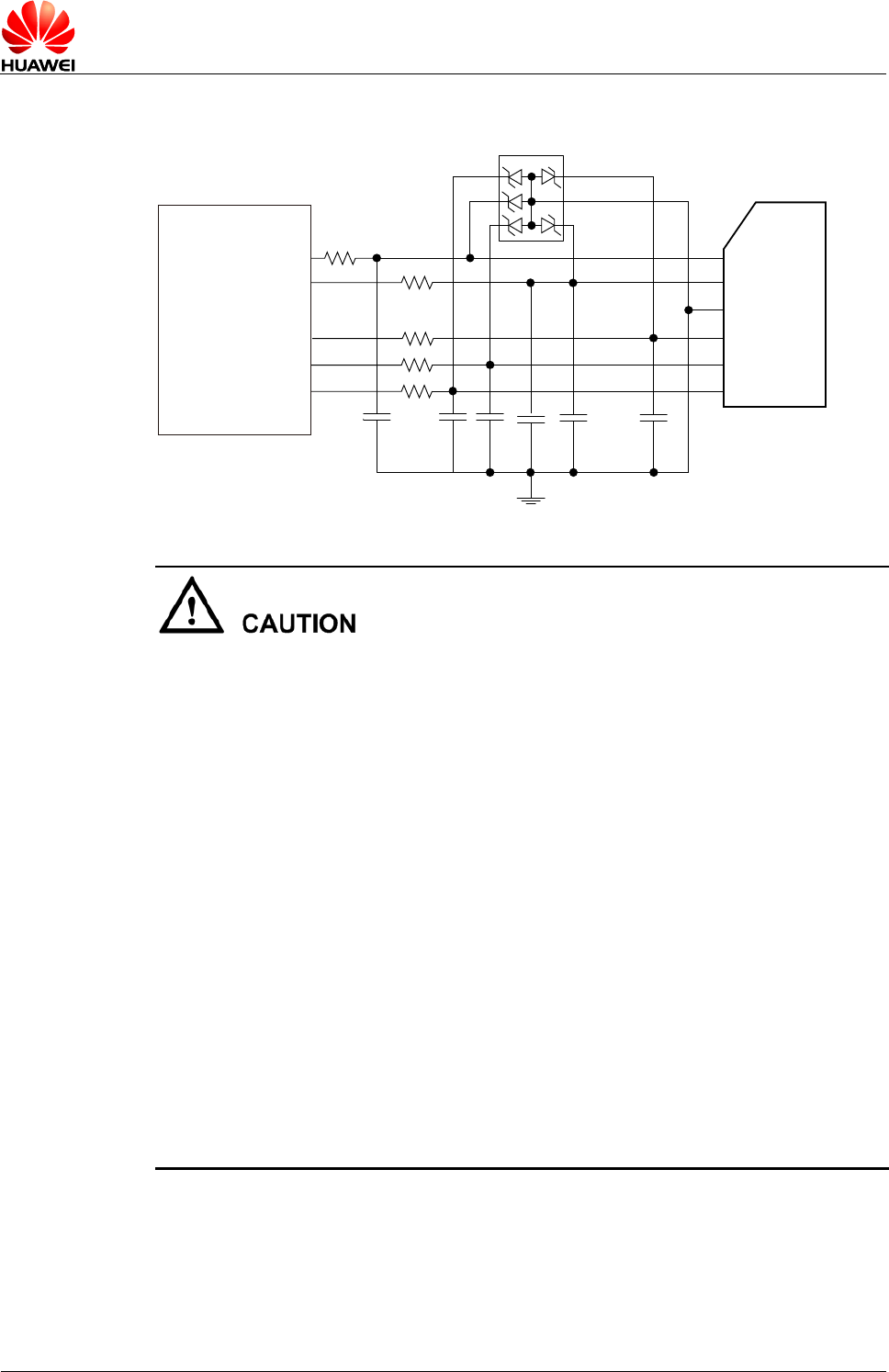
HUAWEI ME909s Series LTE LGA Module
Hardware Guide
Description of the Application Interfaces
Issue 04 (2016-12-21)
Huawei Proprietary and Confidential
Copyright © Huawei Technologies Co., Ltd.
42
Figure 3-19 Circuit of the USIM card interface
USIM
Module
(DCE)
ESD protection
USIM-VCC
USIM-DET
USIM-CLK
USIM-DATA
USIM-RESET
1 µF
0 Ω
0 Ω
0 Ω
0 Ω
33 pF 33 pF 33 pF
33 pF
470 pF
1 kΩ
- To meet the requirements of 3GPP TS 51.010-1 protocols and electromagnetic
compatibility (EMC) authentication, the USIM socket should be placed near the
LGA interface (it is recommended that the PCB circuit connects the LGA interface
and the USIM socket does not exceed 100 mm), because a long circuit may lead to
wave distortion, thus affecting signal quality.
- It is recommended that you wrap the area adjacent to the USIM_CLK and
USIM_DATA signal wires with ground. The Ground pin of the USIM socket and the
Ground pin of the USIM card must be well connected to the power Ground pin
supplying power to the ME909s LGA module.
- A 100 nF capacitor and 1 μF capacitor are placed between the USIM_VCC and
GND pins in a parallel manner (If USIM_VCC circuit is too long, that the larger
capacitance such as 4.7 μF can be employed if necessary). Three 33 pF
capacitors are placed between the USIM_DATA and Ground pins, the
USIM_RESET and Ground pins, and the USIM_CLK and Ground pins in parallel to
filter interference from RF signals.
- It is recommended to take electrostatic discharge (ESD) protection measures near
the USIM card socket. The TVS diode with Vrwm of 5 V and junction capacitance
less than 10 pF must be placed as close as possible to the USIM socket, and the
Ground pin of the ESD protection component is well connected to the power
Ground pin that supplies power to the ME909s LGA module.
- It is recommended to place a 1 kΩ resistor in series on the USIM_DET interface for
ESD protection if USIM_DET is used.
3.8 Audio Interface
ME909s LGA module provides one PCM digital audio interface. Table 3-12 lists the
signals on the digital audio interface.
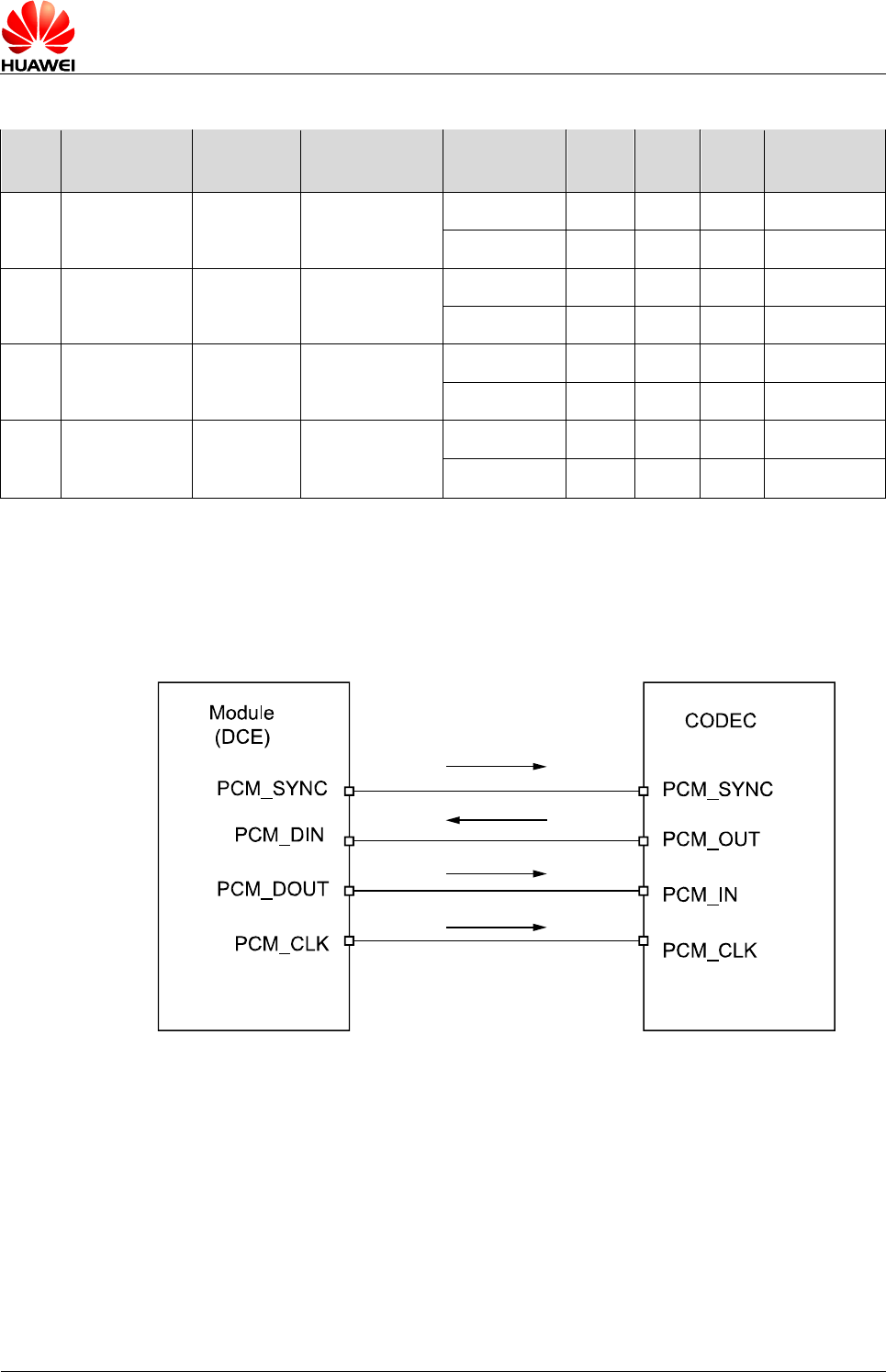
HUAWEI ME909s Series LTE LGA Module
Hardware Guide
Description of the Application Interfaces
Issue 04 (2016-12-21)
Huawei Proprietary and Confidential
Copyright © Huawei Technologies Co., Ltd.
43
Table 3-12 Signals on the digital audio interface
Pin
No.
Pin Name
Pad Type
Description
Parameter
Min.
(V)
Typ.
(V)
Max.
(V)
Comments
5
PCM_SYNC
O
PCM sync
VOH
1.35
1.8
1.98
-
VOL
0
-
0.45
-
6
PCM_DIN
I
PCM data in
VIH
1.17
1.8
1.98
-
VIL
–0.3
-
0.63
-
7
PCM_DOUT
O
PCM data out
VOH
1.35
1.8
1.98
-
VOL
0
-
0.45
-
8
PCM_CLK
O
PCM clock
VOH
1.35
1.8
1.98
-
VOL
0
-
0.45
-
The ME909s LGA PCM interface enables communication with an external codec to
support linear format.
Figure 3-20 Circuit diagram of the interface of the PCM (ME909s LGA module is used as
PCM master)
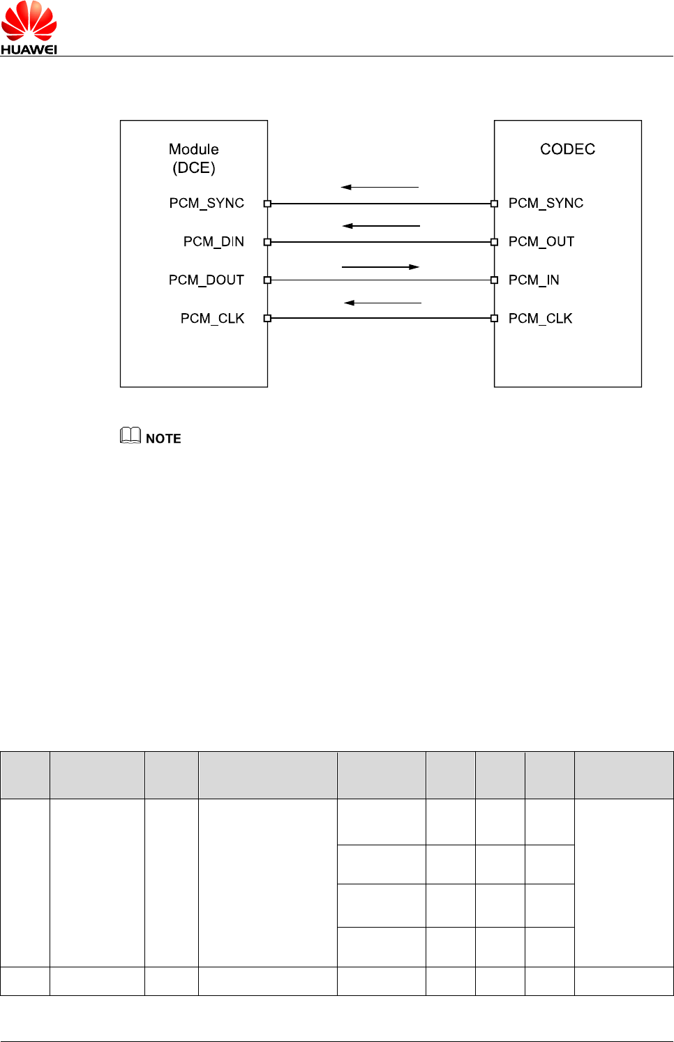
HUAWEI ME909s Series LTE LGA Module
Hardware Guide
Description of the Application Interfaces
Issue 04 (2016-12-21)
Huawei Proprietary and Confidential
Copyright © Huawei Technologies Co., Ltd.
44
Figure 3-21 Circuit diagram of the interface of the PCM (ME909s LGA module is used as
PCM slave)
- The signal level of CODEC must match that of the module.
- ME909s LGA module supports both master and slave mode.
- PCM_CLK: Output when PCM is in master mode; Input when PCM is in slave mode.
- PCM_SYNC: Output when PCM is in master mode; Input when PCM is in slave mode.
- It is recommended that a TVS be used on the related interface, to prevent electrostatic
discharge and protect integrated circuit (IC) components.
3.9 GPIO Interface
The ME909s LGA module provides GPIO pins for customers to use as controlling
signals which are worked at 1.8 V CMOS logic levels. Customers can use AT
command to control the state of logic levels of GPIO output signal. See the HUAWEI
ME909s Series LTE Module AT Command Interface Specification.
Table 3-13 Signals on the GPIO interface
Pin
No.
Pin Name
Pad
Type
Description
Parameter
Min.
(V)
Typ.
(V)
Max.
(V)
Comments
55
GPIO5/USIM
Switch
I/O
General Purpose I/O
pins (Default) or
USIM Switch control
signal.
VOH
1.35
1.8
1.98
The function of
this pin can be
defined as
GPIO or USIM
Switch, while
the USIM
Switch should
be enabled by
AT command.
VOL
0
-
0.45
VIH
1.17
1.8
1.98
VIL
–0.3
-
0.63
113
GPIO3
I/O
General Purpose I/O
VOH
1.35
1.8
1.98
The function of
HUAWEI ME909s Series LTE LGA Module
Hardware Guide
Description of the Application Interfaces
Issue 04 (2016-12-21)
Huawei Proprietary and Confidential
Copyright © Huawei Technologies Co., Ltd.
45
Pin
No.
Pin Name
Pad
Type
Description
Parameter
Min.
(V)
Typ.
(V)
Max.
(V)
Comments
pins (Default)
VOL
0
-
0.45
these pins has
not been
defined.
VIH
1.17
1.8
1.98
VIL
–0.3
-
0.63
51
GPIO2
I/O
General Purpose I/O
pins.
VOH
1.35
1.8
1.98
VOL
0
-
0.45
VIH
1.17
1.8
1.98
VIL
–0.3
-
0.63
105
GPIO1
I/O
General Purpose I/O
pins.
VOH
1.35
1.8
1.98
VOL
0
-
0.45
VIH
1.17
1.8
1.98
VIL
–0.3
-
0.63
109
GPIO4
I/O
General Purpose I/O
pins.
VOH
1.35
1.8
1.98
VOL
0
-
0.45
VIH
1.17
1.8
1.98
VIL
–0.3
-
0.63
43
GPIO1
I/O
General Purpose I/O
pins.
VOH
1.35
1.8
1.98
VOL
0
-
0.45
VIH
1.17
1.8
1.98
VIL
–0.3
-
0.63
46
GPIO2
I/O
General Purpose I/O
pins.
VOH
1.35
1.8
1.98
VOL
0
-
0.45
VIH
1.17
1.8
1.98
VIL
–0.3
-
0.63
When the GPIO interface is used for input, the module will not respond in sleep mode
(it will resume response after being waken up from sleep mode by the WAKEUP_IN
pin) and the module is configured to pull-down inside. In sleep mode, the pull-down
resistance is 5 kΩ–15 kΩ. For the peripheral circuits, see Figure 3-22 .
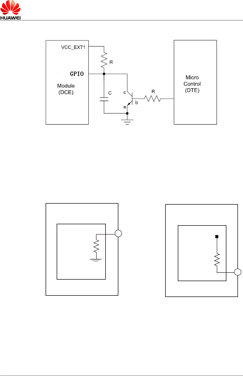
HUAWEI ME909s Series LTE LGA Module
Hardware Guide
Description of the Application Interfaces
Issue 04 (2016-12-21)
Huawei Proprietary and Confidential
Copyright © Huawei Technologies Co., Ltd.
46
Figure 3-22 Reference peripheral circuits when the GPIO interface is used for input
When the GPIO interface is used for output and the module is not in sleep mode, the
drive current is 4 mA. When the module is in sleep mode, the drive current is smaller
than 0.1 mA. The resistance is maintained at 5 kΩ–15 kΩ, as shown in Figure 3-23 .
The output level may be changed if there is a stronger pull-up or pull-down. For the
peripheral circuits, see Figure 3-24 .
Figure 3-23 Maintaining the resistance in sleep mode
BB Chip
Module
(Modem)
Lowoutput level in sleep mode
BB Chip
Module
(Modem)
1.8 V
High output level in sleep mode
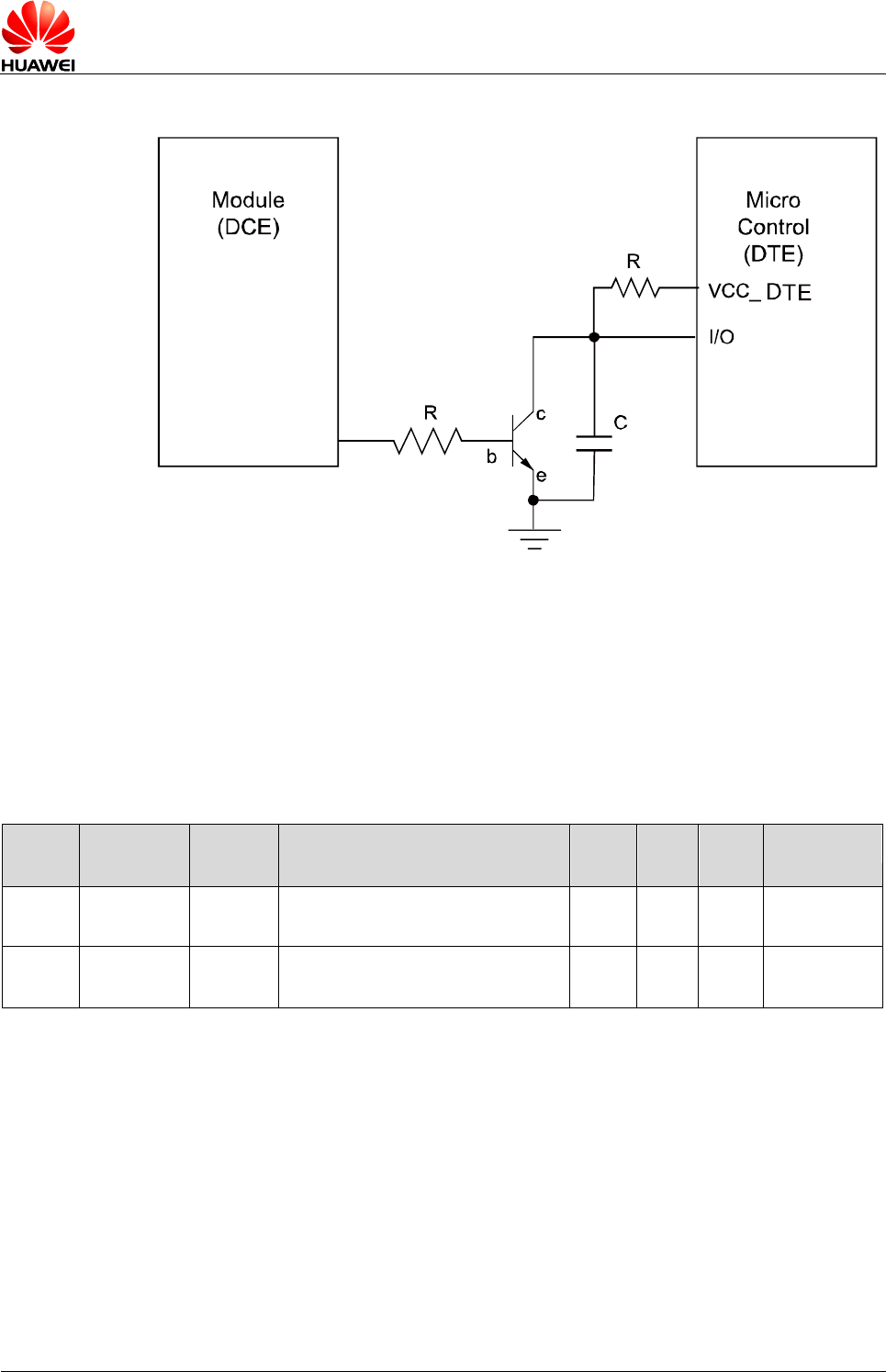
HUAWEI ME909s Series LTE LGA Module
Hardware Guide
Description of the Application Interfaces
Issue 04 (2016-12-21)
Huawei Proprietary and Confidential
Copyright © Huawei Technologies Co., Ltd.
47
Figure 3-24 Reference peripheral circuits when the GPIO interface is used for output
GPIO
3.10 ADC Interface
The ME909s LGA module provides two ADC interfaces. Customers can query their
voltage through AT^ADCREADEX command. For details, you can see HUAWEI
ME909s Series LTE Module AT Command Interface Specification.
Table 3-14 Signals on the ADC interface
PIN
No.
Pin Name
Pad
Type
Description
Min.
(V)
Typ.
(V)
Max.
(V)
Comments
102
ADC_1
AI
Conversion interface for analog
signals to digital signals
0
-
2.5
-
104
ADC_2
AI
Conversion interface for analog
signals to digital signals
0
-
2.5
-
3.11 JTAG Interface
The ME909s LGA module provides Joint Test Action Group (JTAG) interface. Table
3-15 shows the signals on the JTAG interface. It is recommended that route out the 6
pins as test points on the DTE for tracing and debugging.
HUAWEI ME909s Series LTE LGA Module
Hardware Guide
Description of the Application Interfaces
Issue 04 (2016-12-21)
Huawei Proprietary and Confidential
Copyright © Huawei Technologies Co., Ltd.
48
Table 3-15 Signals on the JTAG interface
Pin
No.
Pin Name
Pad
Type
Description
Parameter
Min.
(V)
Typ.
(V)
Max.
(V)
Comments
30
JTAG_TMS
I
JTAG test mode
select
VIH
1.17
1.8
1.98
-
VIL
–0.3
-
0.63
-
36
JTAG_TRST_N
I
JTAG reset
VIH
1.17
1.8
1.98
-
VIL
–0.3
-
0.63
-
42
JTAG_TCK
I
JTAG clock input
VIH
1.17
1.8
1.98
-
VIL
–0.3
-
0.63
-
72
JTAG_TDO
O
JTAG test data output
VOH
1.35
1.8
1.98
-
VOL
0
-
0.45
-
87
JTAG_TDI
I
JTAG test data input
VIH
1.17
1.8
1.98
-
VIL
–0.3
-
0.63
-
93
JTAG_RTCK
O
JTAG return clock,
Pin for trace
connection, it is a
reserved test point for
customers.
VOH
1.35
1.8
2.1
-
VOL
0
-
0.45
-
3.12 RF Antenna Interface
The ME909s LGA module provides two antenna pads (MAIN_ANT and AUX_ANT) for
connecting the external antennas.
Table 3-16 Definition of the antenna pads
Pin
No.
Pin Name
Pad
Type
Description
Parameter
Min.
(V)
Typ.
(V)
Max.
(V)
Comments
107
MAIN_ANT
-
RF MAIN antenna pad
-
-
-
-
-
115
AUX_ANT
-
RF AUX antenna pad
-
-
-
-
-
Route the antenna pad as close as possible to antenna connector. In addition, the
impedance of RF signal traces must be 50 Ω.
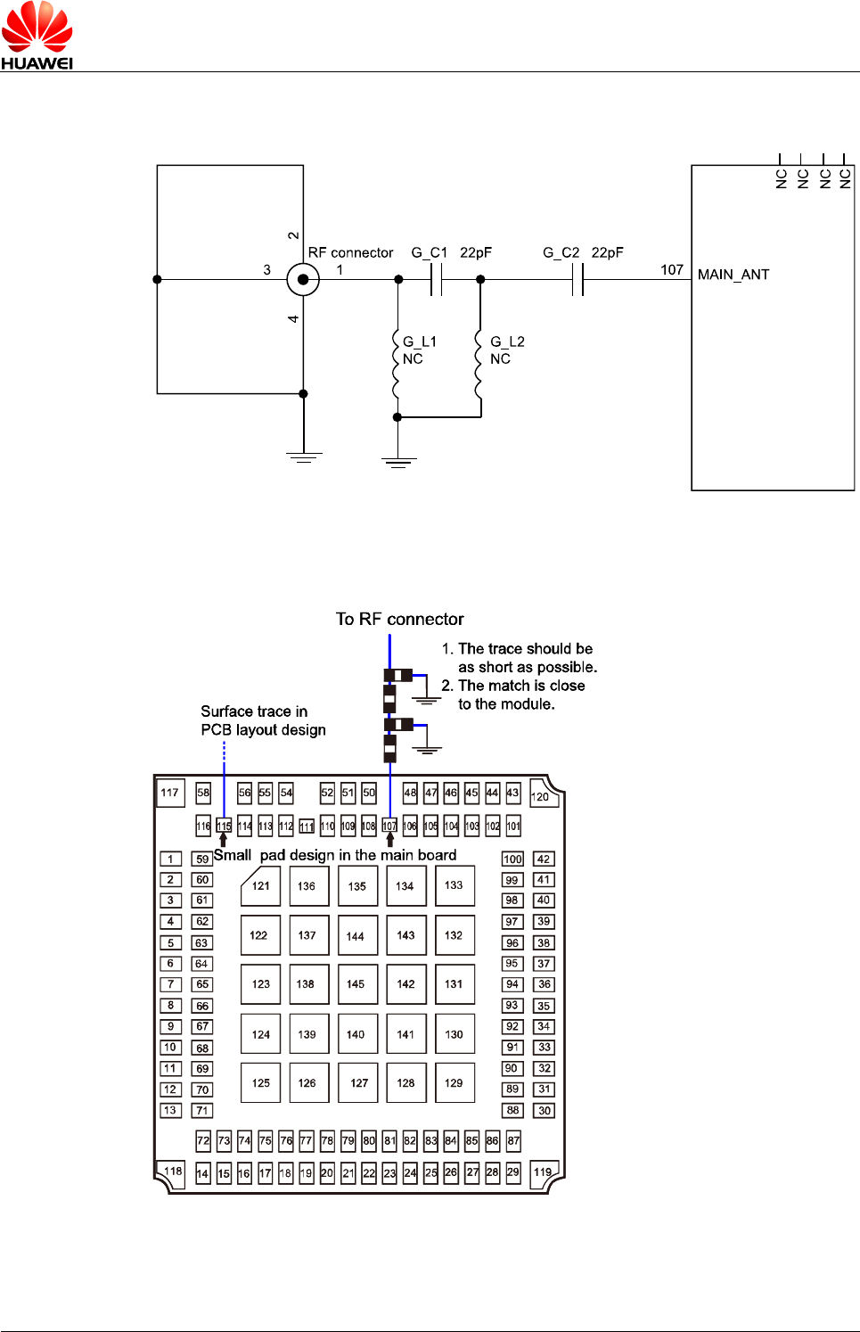
HUAWEI ME909s Series LTE LGA Module
Hardware Guide
Description of the Application Interfaces
Issue 04 (2016-12-21)
Huawei Proprietary and Confidential
Copyright © Huawei Technologies Co., Ltd.
49
Figure 3-25 RF signal trace design about MAIN_ANT for reference (the same for
AUX_ANT)
Figure 3-26 RF signal layout design about MAIN_ANT for reference (the same for
AUX_ANT)
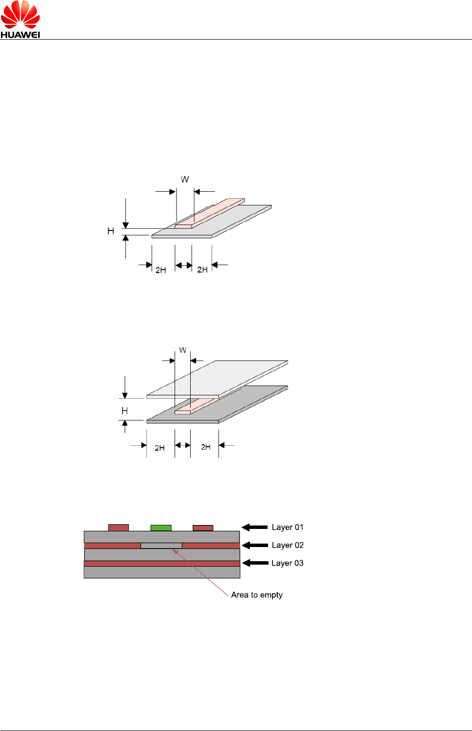
HUAWEI ME909s Series LTE LGA Module
Hardware Guide
Description of the Application Interfaces
Issue 04 (2016-12-21)
Huawei Proprietary and Confidential
Copyright © Huawei Technologies Co., Ltd.
50
For the PCB designed by the user, the impedance of all the RF signal tracks must be
50 Ω. Generally, the impedance depends on the medium factor, track width, and
distance from the floor.
In order to reflect the rules of design, the following figures indicate the complete
structure of the microstrip and stripline with an impedance of 50 Ω as well as the
reference design for stack.
Figure 3-27 Complete structure of the microstrip
Figure 3-28 Complete structure of the stripline
Figure 3-29 Pad for the RF interface
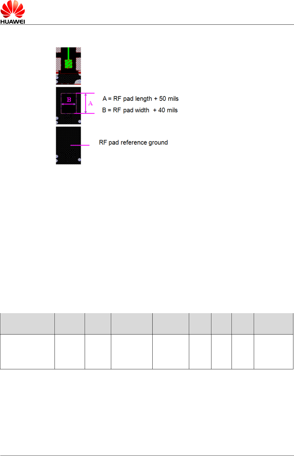
HUAWEI ME909s Series LTE LGA Module
Hardware Guide
Description of the Application Interfaces
Issue 04 (2016-12-21)
Huawei Proprietary and Confidential
Copyright © Huawei Technologies Co., Ltd.
51
Figure 3-30 RF Pad design for ME909s LGA
Please use impedance simulation tool to calculate RF MAIN pad impedance. The RF
MAIN pad dimension of the module is 1.1 mm (L) x 0.9 mm (W). You can get the
impedance with lower than 50 Ω calculated by the impedance simulation tool. Since
the target impedance is 50 Ω for RF trace, the recommended solution is that to carve
out the copper area of the second layer that projected by the RF MAIN pad at top
layer. How many layers should be carved out depend on the PCB permittivity, track
width, and distance from the floor of your own PCB. Our target is to make the RF
MAIN pad impedance as closer to 50 Ω as possible.
3.13 Reserved Interface
The ME909s LGA module provides some reserved pins. All reserved pins cannot be
used by the customer.
Table 3-17 Reserved pin
Pin No.
Pin
Name
Pad
Type
Description
Parameter
Min.
(V)
Typ.
(V)
Max.
(V)
Comments
1-4,14, 16-24, 27,
31, 33, 35, 37, 44,
45, 60–65, 91,
94–99 and 103
Reserved
-
Reserved,
please keep
this pin open.
-
-
-
-
-
3.14 NC Interface
The ME909s LGA module provides some NC pins. All NC pins should not be
connected. Please keep these pins open.
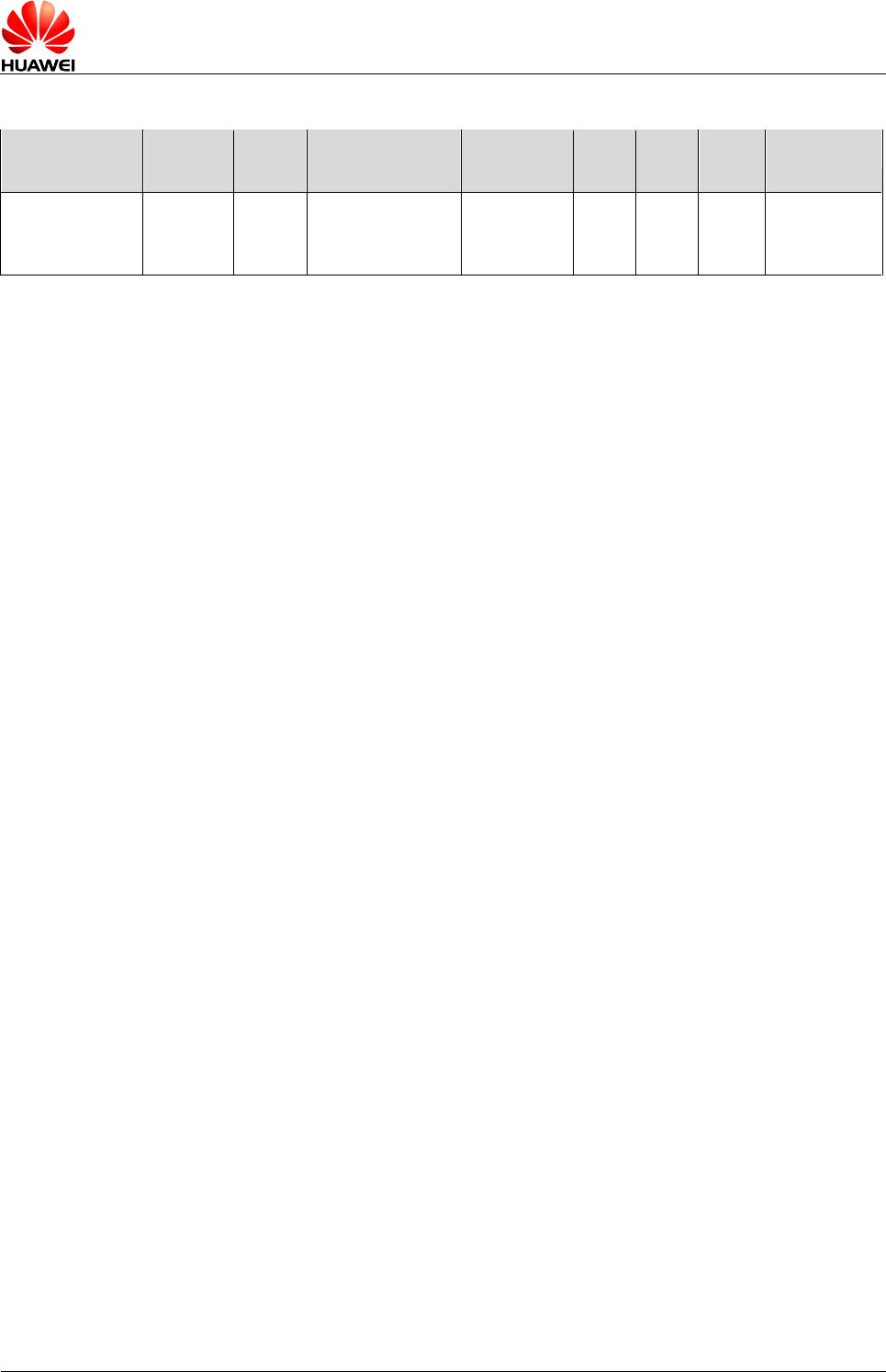
HUAWEI ME909s Series LTE LGA Module
Hardware Guide
Description of the Application Interfaces
Issue 04 (2016-12-21)
Huawei Proprietary and Confidential
Copyright © Huawei Technologies Co., Ltd.
52
Table 3-18 NC pin
Pin No.
Pin
Name
Pad
Type
Description
Parameter
Min.
(V)
Typ.
(V)
Max.
(V)
Comments
25, 26, 38–41,
47, 82–84, 111,
117–120
NC
-
Not connected
-
-
-
-
-
3.15 Test Points Design
In the process of debugging when the module is embedded into the integrated
equipment, test points play an important role. Some problems related to the module
can be quickly resolved when test points are properly designed.
1. The test points below must be designed in the customer board:
− JTAG test points: It is the most common method of debugging.
− USB test points: USB is the most important communication channel between
module and AP (host). Not only test points should be placed, but also a 0 ohm
series resistor should be placed on USB_D+/USB_D- signal. The resistor can
be welded off when necessary, then the USB of module is cut off from AP and
can be connected to PC to do some analyses.
− POWER_ON_OFF, RESIN_N: They are some of the most important signals,
test points should be placed.
− UART2: UART2 is used for printing the log information.
− SD signals: SD signals are used for debugging.
− VBAT: Not only test points should be placed, but also a series magnetic bead
should be placed on VBAT signal. The magnetic bead can be welded off when
necessary, then the power of module is cut off from customer board and can
be connected to external power to do analyses about problems related to
power interference.
− VCC_EXT1: to judge whether the module is powered on or not, just test the
VCC_EXT1.
2. The test points below should be placed according to the requirement in the
customer board: ADC, SLEEP_STATUS, GPIO, PCM, SIM, UART2,
WAKEUP_IN and WAKEUP_OUT, except the two cases below:
− The corresponding signal is not used.
− The corresponding signal is used, but there is already someplace else can be
tested, such as SIM socket pin.
HUAWEI ME909s Series LTE LGA Module
Hardware Guide
RF Specifications
Issue 04 (2016-12-21)
Huawei Proprietary and Confidential
Copyright © Huawei Technologies Co., Ltd.
53
4 RF Specifications
4.1 About This Chapter
This chapter describes the RF specifications of the ME909s LGA module, including:
- Operating Frequencies
- Conducted RF Measurement
- Conducted Rx Sensitivity and Tx Power
- Antenna Design Requirements
- Suggestions about LTE and 2.4 GHz Wi-Fi Co-existence
4.2 Operating Frequencies
Table 4-1 and Table 4-2 show the RF bands supported by ME909s LGA module.
Table 4-1 RF bands of the ME909s-821 LGA module
Operating Band
Tx
Rx
UMTS Band 1
1920 MHz–1980 MHz
2110 MHz–2170 MHz
UMTS Band 5
824 MHz–849 MHz
869 MHz–894 MHz
UMTS Band 8
880 MHz–915 MHz
925 MHz–960 MHz
UMTS Band 9
1749.9 MHz–1784.9 MHz
1844.9 MHz–1879.9 MHz
GSM 900
880 MHz–915 MHz
925 MHz–960 MHz
GSM 1800
1710 MHz–1785 MHz
1805 MHz–1880 MHz
LTE Band 1
1920 MHz–1980 MHz
2110 MHz–2170 MHz
LTE Band 3
1710 MHz–1785 MHz
1805 MHz–1880 MHz
LTE Band 8
880 MHz–915 MHz
925 MHz–960 MHz
LTE Band 38
2570 MHz–2620 MHz
2570 MHz–2620 MHz
LTE Band 39
1880 MHz–1920 MHz
1880 MHz–1920 MHz
HUAWEI ME909s Series LTE LGA Module
Hardware Guide
RF Specifications
Issue 04 (2016-12-21)
Huawei Proprietary and Confidential
Copyright © Huawei Technologies Co., Ltd.
54
Operating Band
Tx
Rx
LTE Band 40[1]
2300 MHz–2400 MHz
2300 MHz–2400 MHz
LTE Band 41[2]
2496 MHz–2690 MHz
2496 MHz–2690 MHz
TD-SCDMA Band 34
2010 MHz–2025 MHz
2010 MHz–2025 MHz
TD-SCDMA Band 39
1880 MHz–1920 MHz
1880 MHz–1920 MHz
- [1]: The module may not meet the RF performance requirements at frequency 2390–2400
MHz in the LTE B40 band.
- [2]: The module may not meet the RF performance requirements at frequency 2496–2555
MHz or 2655–2690 MHz in the LTE B41 band.
Table 4-2 RF bands of the ME909s-120 LGA module
Operating Band
Tx
Rx
UMTS Band 1
1920 MHz–1980 MHz
2110 MHz–2170 MHz
UMTS Band 2
1850 MHz–1910 MHz
1930 MHz–1990 MHz
UMTS Band 5
824 MHz–849 MHz
869 MHz–894 MHz
UMTS Band 8
880 MHz–915 MHz
925 MHz–960 MHz
GSM 850
824 MHz–849 MHz
869 MHz–894 MHz
GSM 900
880 MHz–915 MHz
925 MHz–960 MHz
GSM 1800
1710 MHz–1785 MHz
1805 MHz–1880 MHz
GSM 1900
1850 MHz–1910 MHz
1930 MHz–1990 MHz
LTE Band 1
1920 MHz–1980 MHz
2110 MHz–2170 MHz
LTE Band 2
1850 MHz–1910 MHz
1930 MHz–1990 MHz
LTE Band 3
1710 MHz–1785 MHz
1805 MHz–1880 MHz
LTE Band 4
1710 MHz–1755 MHz
2110 MHz–2155 MHz
LTE Band 5
824 MHz–849 MHz
869 MHz–894 MHz
LTE Band 7
2500 MHz–2570 MHz
2620 MHz–2690 MHz
LTE Band 8
880 MHz–915 MHz
925 MHz–960 MHz
LTE Band 20
832 MHz–862 MHz
791 MHz–821 MHz
HUAWEI ME909s Series LTE LGA Module
Hardware Guide
RF Specifications
Issue 04 (2016-12-21)
Huawei Proprietary and Confidential
Copyright © Huawei Technologies Co., Ltd.
55
4.3 Conducted RF Measurement
4.3.1 Test Environment
Test instrument
R&S CMU200, R&S CMW500, Agilent E5515C, Starpoint
SP6010
Power supply
KEITHLEY 2306; Aglient66319D
RF cable for testing
L08-C014-350 of DRAKA COMTEQ or Rosenberger
Cable length: 29 cm
- The compensation for different frequency bands relates to the cable and the test
environment.
- The instrument compensation needs to be set according to the actual cable conditions.
4.3.2 Test Standards
Huawei modules meet 3GPP test standards. Each module passes strict tests at the
factory and thus the quality of the modules is guaranteed.
4.4 Conducted Rx Sensitivity and Tx Power
4.4.1 Conducted Receive Sensitivity
The conducted receive sensitivity is a key parameter that indicates the receiver
performance of ME909s LGA module.
Table 4-3 and Table 4-4 list the typical tested values of the ME909s LGA module.
Table 4-3 ME909s-821 LGA module conducted Rx sensitivity
Band
Test Value
(Unit: dBm)
Note
GSM 900
–109
BER Class II < 2.44%
GSM 1800
–107
BER Class II < 2.44%
UMTS Band 1
–110.5
BER < 0.1%
UMTS Band 5
–110.5
BER < 0.1%
UMTS Band 8
–110.5
BER < 0.1%
UMTS Band 9
–110.5
BER < 0.1%
LTE Band 1
–103
FDD QPSK throughput > 95%,
10 MHz Bandwidth
LTE Band 3
–102.5
FDD QPSK throughput > 95%,
10 MHz Bandwidth
HUAWEI ME909s Series LTE LGA Module
Hardware Guide
RF Specifications
Issue 04 (2016-12-21)
Huawei Proprietary and Confidential
Copyright © Huawei Technologies Co., Ltd.
56
Band
Test Value
(Unit: dBm)
Note
LTE Band 8
–102.5
FDD QPSK throughput > 95%,
10 MHz Bandwidth
LTE Band 38
–101.5
TDD QPSK throughput > 95%,
10 MHz Bandwidth
LTE Band 39
–102
TDD QPSK throughput > 95%,
10 MHz Bandwidth
LTE Band 40
–101
TDD QPSK throughput > 95%,
10 MHz Bandwidth
LTE Band 41
–101
TDD QPSK throughput > 95%,
10 MHz Bandwidth
TD-SCMDA Band 34
–112
BER < 0.1%
TD-SCMDA Band 39
–112.5
BER < 0.1%
Table 4-4 ME909s-120 LGA module conducted Rx sensitivity
Band
Test Value
(Unit: dBm)
Note
GSM 850
–109
BER Class II < 2.44%
GSM 900
–109
BER Class II < 2.44%
GSM 1800
–108.5
BER Class II < 2.44%
GSM 1900
–109
BER Class II < 2.44%
UMTS Band 1
–111.5
BER < 0.1%
UMTS Band 2
–111.5
BER < 0.1%
UMTS Band 5
–111.5
BER < 0.1%
UMTS Band 8
–111.5
BER < 0.1%
LTE Band 1
–102.5
Throughput ≥ 95%, 10 MHz Bandwidth
LTE Band 2
–102.5
Throughput ≥ 95%, 10 MHz Bandwidth
LTE Band 3
–102
Throughput ≥ 95%, 10 MHz Bandwidth
LTE Band 4
–102
Throughput ≥ 95%, 10 MHz Bandwidth
LTE Band 5
–102.5
Throughput ≥ 95%, 10 MHz Bandwidth
LTE Band 7
–102.5
Throughput ≥ 95%, 10 MHz Bandwidth
LTE Band 8
–102.5
Throughput ≥ 95%, 10 MHz Bandwidth
LTE Band 20
–102.5
Throughput ≥ 95%, 10 MHz Bandwidth
HUAWEI ME909s Series LTE LGA Module
Hardware Guide
RF Specifications
Issue 04 (2016-12-21)
Huawei Proprietary and Confidential
Copyright © Huawei Technologies Co., Ltd.
57
- The test values are the average of some test samples.
- LTE sensitivity is tested in SIMO (Main + AUX).
4.4.2 Conducted Transmit Power
The conducted transmit power is another indicator that measures the performance of
ME909s LGA module. The conducted transmit power refers to the maximum power
that the module tested at the antenna pad can transmit. According to the 3GPP
protocol, the required transmit power varies with the power class.
Table 4-5 and Table 4-6 list the required ranges of the conducted transmit power of
ME909s LGA module.
Table 4-5 ME909s-821 LGA module conducted Tx power
Band
Typical Value (Unit: dBm)
Note (Unit: dB)
GSM 900
GMSK (1Tx Slot)
32.5
±1.5
8PSK (1Tx Slot)
27
±1.5
GSM 1800
GMSK (1Tx Slot)
29.5
±1.5
8PSK (1Tx Slot)
26
±1.5
UMTS Band 1
23.5
±1
UMTS Band 5
23.5
±1
UMTS Band 8
23.5
±1
UMTS Band 9
23.5
±1
TD-SCDMA Band 34
23.5
±1
TD-SCDMA Band 39
23.5
±1
TDD LTE Band 38
23
±1.5
TDD LTE Band 39
23
±1.5
TDD LTE Band 40
23
±1.5
TDD LTE Band 41
23
±1.5
FDD LTE Band 1
23
±1.5
FDD LTE Band 3
23
±1.5
FDD LTE Band 8
23
±1.5
Table 4-6 ME909s-120 LGA module conducted Tx power
Band
Typical Value (Unit: dBm)
Note (Unit: dB)
GSM 850
GMSK (1Tx Slot)
32.5
±1.5
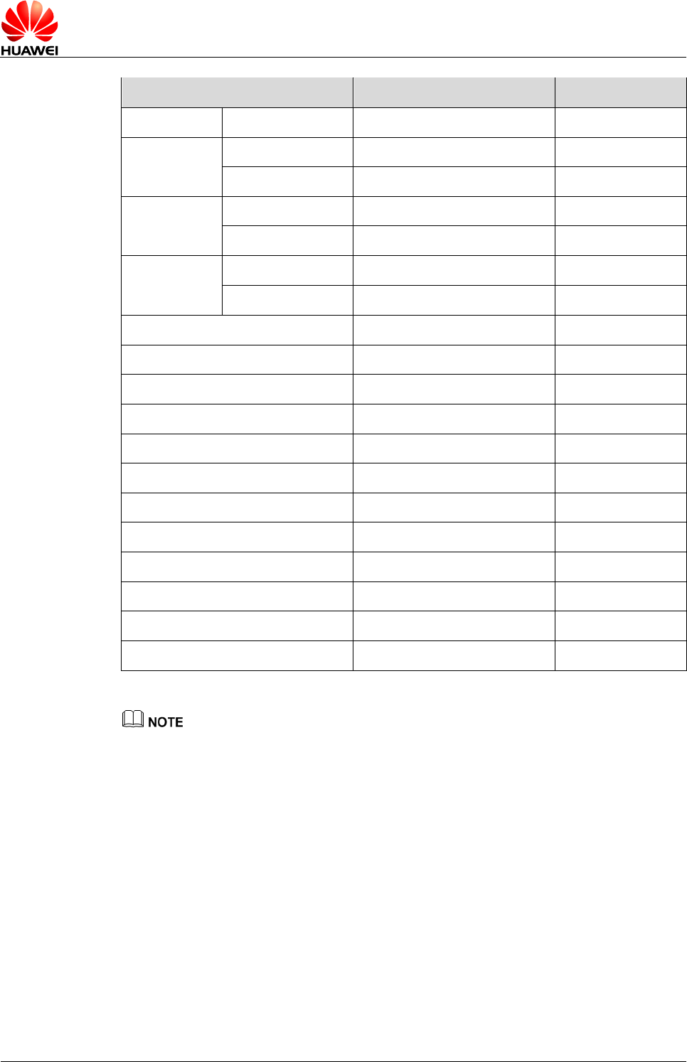
HUAWEI ME909s Series LTE LGA Module
Hardware Guide
RF Specifications
Issue 04 (2016-12-21)
Huawei Proprietary and Confidential
Copyright © Huawei Technologies Co., Ltd.
58
Band
Typical Value (Unit: dBm)
Note (Unit: dB)
8PSK (1Tx Slot)
27
±1.5
GSM 900
GMSK (1Tx Slot)
32.5
±1.5
8PSK (1Tx Slot)
27
±1.5
GSM 1800
GMSK (1Tx Slot)
29.5
±1.5
8PSK (1Tx Slot)
26
±1.5
GSM 1900
GMSK (1Tx Slot)
29.5
±1.5
8PSK (1Tx Slot)
26
±1.5
UMTS Band 1
23.5
±1
UMTS Band 2
23.5
±1
UMTS Band 5
23.5
±1
UMTS Band 8
23.5
±1
LTE Band 1
23
±1.5
LTE Band 2
23
±1.5
LTE Band 3
23
±1.5
LTE Band 4
23
±1.5
LTE Band 5
23
±1.5
LTE Band 7
23
±1.5
LTE Band 8
23
±1.5
LTE Band 20
23
±1.5
Maximum Power Reduction (MPR and AMPR) of LTE is according to 3GPP TS 36.521-1.
4.5 Antenna Design Requirements
4.5.1 Antenna Design Indicators
Antenna Efficiency
Antenna efficiency is the ratio of the input power to the radiated or received power of
an antenna. The radiated power of an antenna is always lower than the input power
due to the following antenna losses: return loss, material loss, and coupling loss. The
efficiency of an antenna relates to its electrical dimensions. To be specific, the
antenna efficiency increases with the electrical dimensions. In addition, the
transmission line from the antenna port of ME909s LGA to the antenna is also part of

HUAWEI ME909s Series LTE LGA Module
Hardware Guide
RF Specifications
Issue 04 (2016-12-21)
Huawei Proprietary and Confidential
Copyright © Huawei Technologies Co., Ltd.
59
the antenna. The line loss increases with the line length and the frequency. It is
recommended that the line loss is as low as possible.
The following antenna efficiency (free space) is recommended for ME909s LGA to
ensure high radio performance of the module:
- Efficiency of the primary antenna: ≥ 40% (below 960 MHz); ≥ 50% (over 1710
MHz)
- Efficiency of the diversity antenna: ≥ half of the efficiency of the primary
antenna in receiving band
In addition, the efficiency should be tested with the transmission line.
S11 (VSWR)
S11 indicates the degree to which the input impedance of an antenna matches the
reference impedance (50 Ω). S11 shows the resonance feature and impedance
bandwidth of an antenna. Voltage standing wave ratio (VSWR) is another expression
of S11. S11 relates to the antenna efficiency. S11 can be measured with a vector
analyzer.
The following S11 value is recommended for the antenna of ME909s LGA module:
- S11 of the primary antenna: ≤ –6 dB
- S11 of the diversity antenna: ≤ –6 dB
In addition, S11 is less important than the efficiency, and S11 has weak correlation to
wireless performance.
Isolation
For a wireless device with multiple antennas, the power of different antennas is
coupled with each other. Antenna isolation is used to measure the power coupling.
The power radiated by an antenna might be received by an adjacent antenna, which
decreases the antenna radiation efficiency and affects the running of other devices. To
avoid this problem, evaluate the antenna isolation as sufficiently as possible at the
early stage of antenna design.
Antenna isolation depends on the following factors:
- Distance between antennas
- Antenna type
- Antenna direction
The primary antenna must be placed as near as possible to the ME909s LGA to
minimize the cable length. The diversity antenna needs to be installed
perpendicularly to the primary antenna. The diversity antenna can be placed farther
away from the ME909s LGA. Antenna isolation can be measured with a two-port
vector network analyzer.
The following antenna isolation is recommended for the antennas on laptops:
- Isolation between the primary and diversity antennas: ≤ –12 dB
- Isolation between the primary (diversity) antenna and the Wi-Fi antenna: ≤
–15 dB

HUAWEI ME909s Series LTE LGA Module
Hardware Guide
RF Specifications
Issue 04 (2016-12-21)
Huawei Proprietary and Confidential
Copyright © Huawei Technologies Co., Ltd.
60
Polarization
The polarization of an antenna is the orientation of the electric field vector that rotates
with time in the direction of maximum radiation.
The linear polarization is recommended for the antenna of ME909s LGA.
Radiation Pattern
The radiation pattern of an antenna reflects the radiation features of the antenna in the
remote field region. The radiation pattern of an antenna commonly describes the
power or field strength of the radiated electromagnetic waves in various directions
from the antenna. The power or field strength varies with the angular coordinates (θ
and φ), but is independent of the radial coordinates.
The radiation pattern of half wave dipole antennas is omnidirectional in the horizontal
plane, and the incident waves of base stations are often in the horizontal plane. For
this reason, the receiving performance is optimal.
The following radiation patterns are recommended for the antenna of ME909s LGA.
Primary/diversity antenna: omnidirectional
In addition, the diversity antenna’s pattern should be complementary with the primary
antenna's pattern.
Gain and Directivity
The radiation pattern of an antenna represents the field strength of the radiated
electromagnetic waves in all directions, but not the power density that the antenna
radiates in the specific direction. The directivity of an antenna, however, measures the
power density that the antenna radiates.
Gain, as another important parameter of antennas, correlates closely to the directivity.
The gain of an antenna takes both the directivity and the efficiency of the antenna into
account. The appropriate antenna gain prolongs the service life of relevant batteries.
The following antenna gain is recommended for ME909s LGA.
Gain of the primary/diversity antenna ≤ 2.5 dBi
ECC of the Antenna
ECC is short for Envelope Correlation Coefficient. It is the cross-correlation value of
the complex patterns of the master and diversity antenna. It indicates how similar the
magnitude and the phase patterns of the two antennas are. If two antennas have no
similarity, the ECC should be zero. Actually, the less ECC, the better diversity
performance.
The following ECC is recommended for ME909s LGA module.
- ECC ≤ 0.5 (working frequency below 0.96 GHz)
- ECC ≤ 0.3 (working frequency above 1.4 GHz)
HUAWEI ME909s Series LTE LGA Module
Hardware Guide
RF Specifications
Issue 04 (2016-12-21)
Huawei Proprietary and Confidential
Copyright © Huawei Technologies Co., Ltd.
61
- The antenna consists of the antenna body and the relevant RF transmission line. Take the
RF transmission line into account when measuring any of the preceding antenna indicators.
- Huawei cooperates with various famous antenna suppliers who are able to make
suggestions on antenna design, for example, Amphenol, Skycross, etc.
4.5.2 Interference
Besides the antenna performance, the interference on the user board also affects the
radio performance (especially the TIS) of the module. To guarantee high performance
of the module, the interference sources on the user board must be properly controlled.
On the user board, there are various interference sources, such as the LCD, CPU,
audio circuits, and power supply. All the interference sources emit interference signals
that affect the normal operation of the module. For example, the module sensitivity
can be decreased due to interference signals. Therefore, during the design, you need
to consider how to reduce the effects of interference sources on the module. You can
take the following measures: Use an LCD with optimized performance; shield the LCD
interference signals; shield the signal line of the board; or design filter circuits.
Huawei is able to make technical suggestions on radio performance improvement of
the module.
4.5.3 Antenna Requirements
The antenna for ME909s LGA module must fulfill the following requirements:
Table 4-7 ME909s LGA module antenna requirements
Antenna Requirements
Frequency range
Depending on frequency band(s) provided by the network
operator, the customer must use the most suitable
antenna for that/those band(s)
Bandwidth of primary
antenna
ME909s-821
250 MHz in UMTS Band 1; LTE Band 1
170 MHz in GSM 1800; LTE Band 3
70 MHz in UMTS Band 5;
80 MHz in GSM 900; UMTS Band 8; LTE Band 8
130 MHz in UMTS Band 9
50 MHz in LTE Band 38
40 MHz in LTE Band 39
100 MHz in LTE Band 40
194 MHz in LTE Band 41
15 MHz in TD-SCDMA Band 34
40 MHz in TD-SCDMA Band 39
ME909s-120
250 MHz in UMTS Band 1; LTE Band 1
140 MHz in GSM 1900; UMTS Band 2; LTE Band 2
170 MHz in GSM 1800; LTE Band 3
HUAWEI ME909s Series LTE LGA Module
Hardware Guide
RF Specifications
Issue 04 (2016-12-21)
Huawei Proprietary and Confidential
Copyright © Huawei Technologies Co., Ltd.
62
Antenna Requirements
445 MHz in LTE Band 4
70 MHz in GSM 850; UMTS Band 5; LTE Band 5
190MHz in LTE Band 7
80 MHz in GSM 900; UMTS Band 8; LTE Band 8
71 MHz in LTE Band 20
Bandwidth of
secondary antenna
ME909s-821
60 MHz in UMTS Band 1; LTE Band 1
75 MHz in LTE Band 3
25 MHz in UMTS Band 5
35 MHz in UMTS Band 8; LTE Band 8
30 MHz in UMTS Band 9
50 MHz in LTE Band 38
40 MHz in LTE Band 39
100 MHz in LTE Band 40
194 MHz in LTE Band 41
ME909s-120
60 MHz in UMTS Band 1; LTE Band 1
60 MHz in UMTS Band 2; LTE Band 2
75 MHz in LTE Band 3
45 MHz in LTE Band 4
25 MHz in UMTS Band 5; LTE Band 5
70 MHz in LTE Band 7
35 MHz in UMTS Band 8; LTE Band 8
30 MHz in LTE Band 20
Gain
≤ 2.5 dBi
Impedance
50 Ω
VSWR absolute max
≤ 3:1
VSWR recommended
≤ 2:1
4.6 Suggestions about LTE and 2.4 GHz Wi-Fi Co-existence
4.6.1 Theory Analysis
The band gap between LTE Band 38/40/41 and Wi-Fi (2.4 G) is very narrow just as
shown as below.
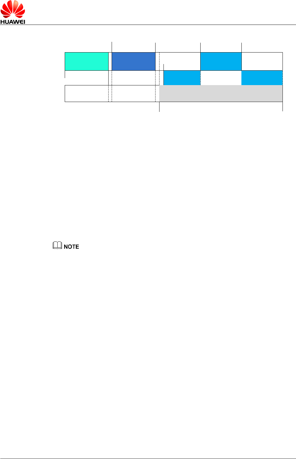
HUAWEI ME909s Series LTE LGA Module
Hardware Guide
RF Specifications
Issue 04 (2016-12-21)
Huawei Proprietary and Confidential
Copyright © Huawei Technologies Co., Ltd.
63
B40 TX/RX WIFI TX/RX B38 TX/RX
B41 TX/RX
2300MHz 2400MHz
2401MHz 2495MHz 2570MHz 2620MHz
2500MHz
2496MHz 2690MHz
B7 uplink B7 downlink
The two systems interfere with each other because of nonlinear characteristic of LTE
Band 38/40/41 and Wi-Fi transmitter. The main impacts are as follows:
1. LTE Band transmitter spurious in Wi-Fi Band impacts on the sensitivity of Wi-Fi
receiver.
2. LTE Band output power can block Wi-Fi receiver.
3. Wi-Fi transmitter spurious in LTE Band impacts on the sensitivity of LTE Bands.
4. Wi-Fi output power can block LTE Band receiver.
According to the theoretical analysis, in order to achieve the co-existence between
Wi-Fi and LTE, the rejection between Wi-Fi and LTE Band 41 or Band 40 needs to be
over 60 dB. (The analysis is based on the Wi-Fi chip Broadcom BCM432XX, the
co-existence design depends on the customer’s Wi-Fi chipset specification.)
In fact, the current devices cannot meet this requirement, so we need to increase the isolation
between antennas and disable some channels.
4.6.2 Suggestions about the Interference
These risks have been taken into consideration in the design of the ME909s LGA
module. The system design also should be paid attention:
1. It is recommended that the system should be added Wi-Fi SAW filter to
guarantee good attenuation in the LTE transmit Band (including Band 38, Band
40, Band 41), otherwise, LTE Band output power will block Wi-Fi receiver.
2. The good isolation between LTE antenna and Wi-Fi antenna is more than 25 dB.
3. Two ways above can help to make the isolation to be 60 dB. If they are still not
enough, some channels may need to be disabled.
HUAWEI ME909s Series LTE LGA Module
Hardware Guide
Electrical and Reliability Features
Issue 04 (2016-12-21)
Huawei Proprietary and Confidential
Copyright © Huawei Technologies Co., Ltd.
64
5 Electrical and Reliability Features
5.1 About This Chapter
This chapter describes the electrical and reliability features in the ME909s LGA
module, including:
- Absolute Ratings
- Operating and Storage Temperatures
- Power Supply Features
- Reliability Features
- EMC and ESD Features
5.2 Absolute Ratings
Table 5-1 lists the absolute ratings for the ME909s LGA module. Using the ME909s
LGA module beyond these conditions may result in permanent damage to the module.
Table 5-1 Absolute ratings
Symbol
Specification
Min.
Max.
Unit
VBAT
External power voltage
–0.3
4.5
V
VI
Digital input voltage
–0.3
2.3
V
5.3 Operating and Storage Temperatures
Table 5-2 lists the operating and storage temperatures for the ME909s LGA module.
HUAWEI ME909s Series LTE LGA Module
Hardware Guide
Electrical and Reliability Features
Issue 04 (2016-12-21)
Huawei Proprietary and Confidential
Copyright © Huawei Technologies Co., Ltd.
65
Table 5-2 Operating and storage temperatures
Specification
Min.
Max.
Unit
Normal working temperatures
–30
+75
°C
Extended temperatures[1]
–40
+85
°C
Ambient temperature for storage
–40
+85
°C
[1]: When the ME909s LGA module works in the range from –40°C to –30°C or +75°C to +85°C ,
NOT all their RF performances comply with 3GPP specifications.
5.4 Power Supply Features
5.4.1 Input Power Supply
Table 5-3 lists the requirements for input power of the ME909s LGA module.
Table 5-3 Requirements for input power
Parameter
Min.
Typ.
Max.
Ripple
Unit
VBAT
3.2
3.8
4.2
0.05
V
Figure 5-1 Power Supply During Burst Emission
The VBAT minimum value must be guaranteed during the burst (with 2.75 A Peak in GPRS or
GSM mode).
Table 5-4 Requirements for input current
Power
Peak (GSM 1 slot)
Normal (WCDMA)
Normal (LTE 23 dbm)
VBAT
2750 mA
1100 mA
1100 mA
HUAWEI ME909s Series LTE LGA Module
Hardware Guide
Electrical and Reliability Features
Issue 04 (2016-12-21)
Huawei Proprietary and Confidential
Copyright © Huawei Technologies Co., Ltd.
66
5.4.2 Power Consumption
The power consumptions of ME909s LGA module in different scenarios are
respectively listed in Table 5-5 to Table 5-11 .
The power consumption listed in this section is tested when the power supply of
ME909s LGA module is 3.8 V, and all of test values are measured at room
temperature.
Table 5-5 Averaged power off DC power consumption
Description
Test Value (Unit: µA )
Notes/Configuration
Typical
Power off
65
Normal voltage (3.8 V) is ON while
power on event is not triggered.
Table 5-6 Averaged standby DC power consumption of ME909s-821 LGA module
Description
Bands
Test Value (Unit: mA)
Notes/Configuration
Typical
Sleep
LTE
LTE bands
1.9
Module is powered up.
Paging cycle=256 (2.56s)
Module is registered on the
network.
USB is in suspend
TD-SCDMA
TD-SCDMA
bands
2.5
Module is powered up.
DRX cycle=8 (2.56s)
Module is registered on the
network.
USB is in suspend
HSPA+/WCDMA
UMTS bands
1.7
Module is powered up
DRX cycle=8 (1.28s)
Module is registered on the
network.
USB is in suspend
GPRS/EDGE
GSM bands
2.1
Module is powered up
MFRMS=5 (1.175s)
Module is registered on the
network.
USB is in suspend.
HUAWEI ME909s Series LTE LGA Module
Hardware Guide
Electrical and Reliability Features
Issue 04 (2016-12-21)
Huawei Proprietary and Confidential
Copyright © Huawei Technologies Co., Ltd.
67
Description
Bands
Test Value (Unit: mA)
Notes/Configuration
Typical
Idle
LTE
LTE bands
48
Module is powered up.
Paging cycle=256 (2.56s)
Module is registered on the
network, no data is
transmitted.
USB is in active.
TD-SCDMA
TD-SCDMA
bands
50
Module is powered up.
DRX cycle=8 (2.56s)
Module is registered on the
network.
USB is in active
HSPA+/WCDMA
UMTS bands
55
Module is powered up
DRX cycle=8 (1.28s)
Module is registered on the
network, no data is
transmitted
USB is in active.
GPRS/EDGE
GSM bands
55
Module is powered up
MFRMS=5 (1.175s)
Module is registered on the
network, no data is
transmitted
USB is in active.
Table 5-7 Averaged standby DC power consumption of ME909s-120 LGA module
Description
Bands
Test Value (Unit: mA)
Notes/Configuration
Typical
Sleep
LTE
LTE bands
1.85
Module is powered up.
Paging cycle=256 (2.56s)
Module is registered on the
network.
USB is in suspend.
HSPA/WCDMA
UMTS bands
1.5
Module is powered up
DRX cycle=8 (1.28s)
Module is registered on the
network.
USB is in suspend.
HUAWEI ME909s Series LTE LGA Module
Hardware Guide
Electrical and Reliability Features
Issue 04 (2016-12-21)
Huawei Proprietary and Confidential
Copyright © Huawei Technologies Co., Ltd.
68
Description
Bands
Test Value (Unit: mA)
Notes/Configuration
Typical
GPRS/EDGE
GSM bands
1.87
Module is powered up
MFRMS=5 (1.175s)
Module is registered on the
network.
USB is in suspend.
Idle
LTE
LTE bands
48
Module is powered up.
Paging cycle=256 (2.56s)
Module is registered on the
network, no data is
transmitted.
USB is in active.
HSPA/WCDMA
UMTS bands
47
Module is powered up
DRX cycle=8 (1.28s)
Module is registered on the
network, no data is
transmitted
USB is in active.
GPRS/EDGE
GSM bands
48
Module is powered up
MFRMS=5 (1.175s)
Module is registered on the
network.
no data is transmitted
USB is in active.
Table 5-8 Averaged Data Transmission DC power consumption of ME909s-821 LGA
module (LTE/HSPA/WCDMA/TD-SCDMA)
Description
Band
Test Value (Unit: mA)
Notes/Configuration
Typical
WCDMA
Band 1
(IMT 2100)
188
0 dBm Tx Power
216
10 dBm Tx Power
603
23.5 dBm Tx Power
Band 5
(850MHz)
181
0 dBm Tx Power
199
10 dBm Tx Power
501
23.5 dBm Tx Power
Band 8
188
0 dBm Tx Power
HUAWEI ME909s Series LTE LGA Module
Hardware Guide
Electrical and Reliability Features
Issue 04 (2016-12-21)
Huawei Proprietary and Confidential
Copyright © Huawei Technologies Co., Ltd.
69
Description
Band
Test Value (Unit: mA)
Notes/Configuration
Typical
(900 MHz)
207
10 dBm Tx Power
504
23.5 dBm Tx Power
Band 9
(J1700)
212
0 dBm Tx Power
289
10 dBm Tx Power
719
23.5 dBm Tx Power
HSPA
Band 1
(IMT 2100)
179
0 dBm Tx Power
213
10 dBm Tx Power
578
23.5 dBm Tx Power
Band 5
(850MHz)
172
0 dBm Tx Power
189
10 dBm Tx Power
439
23.5 dBm Tx Power
Band 8
(900 MHz)
177
0 dBm Tx Power
201
10 dBm Tx Power
489
23.5 dBm Tx Power
Band 9
(J1700)
221
0 dBm Tx Power
300
10 dBm Tx Power
743
23.5 dBm Tx Power
TDD LTE
Band 38
195
0 dBm Tx Power
242
10 dBm Tx Power
400
23 dBm Tx Power
Band 39
182
0 dBm Tx Power
213
10 dBm Tx Power
273
23 dBm Tx Power
Band 40
195
0 dBm Tx Power
242
10 dBm Tx Power
438
23 dBm Tx Power
Band 41
195
0 dBm Tx Power
246
10 dBm Tx Power
405
23 dBm Tx Power
FDD LTE
Band 1
263
0 dBm Tx Power
HUAWEI ME909s Series LTE LGA Module
Hardware Guide
Electrical and Reliability Features
Issue 04 (2016-12-21)
Huawei Proprietary and Confidential
Copyright © Huawei Technologies Co., Ltd.
70
Description
Band
Test Value (Unit: mA)
Notes/Configuration
Typical
315
10 dBm Tx Power
623
23 dBm Tx Power
Band 3
268
0 dBm Tx Power
338
10 dBm Tx Power
807
23 dBm Tx Power
Band 8
264
0 dBm Tx Power
298
10 dBm Tx Power
520
23 dBm Tx Power
TD-SCDMA
Band 34
84
0 dBm Tx Power
87
10 dBm Tx Power
132
23 dBm Tx Power
Band 39
95
0 dBm Tx Power
101
10 dBm Tx Power
133
23 dBm Tx Power
Table 5-9 Averaged Data Transmission DC power consumption of ME909s-120 LGA
module (WCDMA/HSDPA/LTE)
Description
Band
Test Value (Unit: mA)
Notes/Configuration
Typical
WCDMA
Band 1
(IMT 2100)
190
0 dBm Tx Power
225
10 dBm Tx Power
690
23.5 dBm Tx Power
Band 2
(PCS 1900)
187
0 dBm Tx Power
220
10 dBm Tx Power
670
23.5 dBm Tx Power
Band 5
(850 MHz)
180
0 dBm Tx Power
215
10 dBm Tx Power
555
23.5 dBm Tx Power
Band 8
185
0 dBm Tx Power
HUAWEI ME909s Series LTE LGA Module
Hardware Guide
Electrical and Reliability Features
Issue 04 (2016-12-21)
Huawei Proprietary and Confidential
Copyright © Huawei Technologies Co., Ltd.
71
Description
Band
Test Value (Unit: mA)
Notes/Configuration
Typical
(900 MHz)
220
10 dBm Tx Power
635
23.5 dBm Tx Power
HSDPA
Band 1
(IMT2100)
205
0 dBm Tx Power
243
10 dBm Tx Power
631
23.5 dBm Tx Power
Band 2
(PCS 1900)
202
0 dBm Tx Power
238
10 dBm Tx Power
580
23.5 dBm Tx Power
Band 5
(850 MHz)
200
0 dBm Tx Power
235
10 dBm Tx Power
535
23.5 dBm Tx Power
Band 8
(900 MHz)
205
0 dBm Tx Power
247
10 dBm Tx Power
575
23.5 dBm Tx Power
LTE
Band 1
270
0 dBm Tx Power
330
10 dBm Tx Power
725
23 dBm Tx Power
Band 2
275
0 dBm Tx Power
330
10 dBm Tx Power
715
23 dBm Tx Power
Band 3
273
0 dBm Tx Power
340
10 dBm Tx Power
735
23 dBm Tx Power
Band 4
276
0 dBm Tx Power
340
10 dBm Tx Power
705
23 dBm Tx Power
Band 5
280
0 dBm Tx Power
642
10 dBm Tx Power
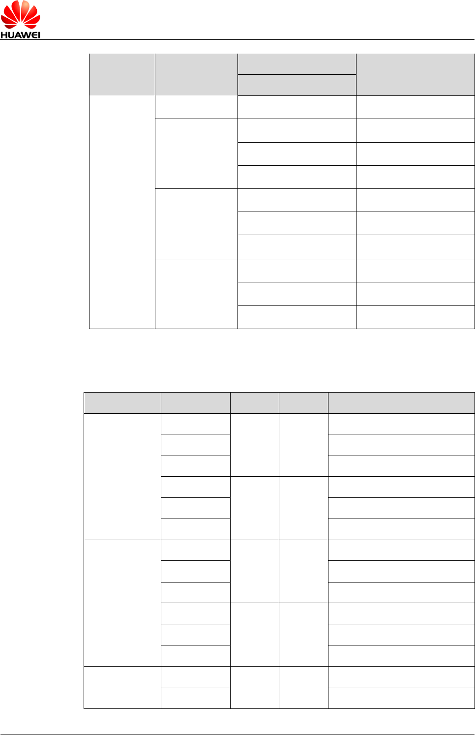
HUAWEI ME909s Series LTE LGA Module
Hardware Guide
Electrical and Reliability Features
Issue 04 (2016-12-21)
Huawei Proprietary and Confidential
Copyright © Huawei Technologies Co., Ltd.
72
Description
Band
Test Value (Unit: mA)
Notes/Configuration
Typical
725
23 dBm Tx Power
Band 7
280
0 dBm Tx Power
340
10 dBm Tx Power
725
23 dBm Tx Power
Band 8
278
0 dBm Tx Power
330
10 dBm Tx Power
645
23 dBm Tx Power
Band 20
280
0 dBm Tx Power
330
10 dBm Tx Power
665
23 dBm Tx Power
Table 5-10 Averaged DC power consumption of ME909s-821 LGA module
(GPRS/EDGE)
Description
Test Value
Units
PCL
Configuration
GPRS 900
314
mA
5
1 Up/1 Down
468
2 Up/1 Down
627
4 Up/1 Down
169
mA
10
1 Up/1 Down
257
2 Up/1 Down
430
4 Up/1 Down
GPRS 1800
190
mA
0
1 Up/1 Down
275
2 Up/1 Down
363
4 Up/1 Down
107
mA
10
1 Up/1 Down
133
2 Up/1 Down
190
4 Up/1 Down
EDGE 900
213
mA
8
1 Up/1 Down
292
2 Up/1 Down
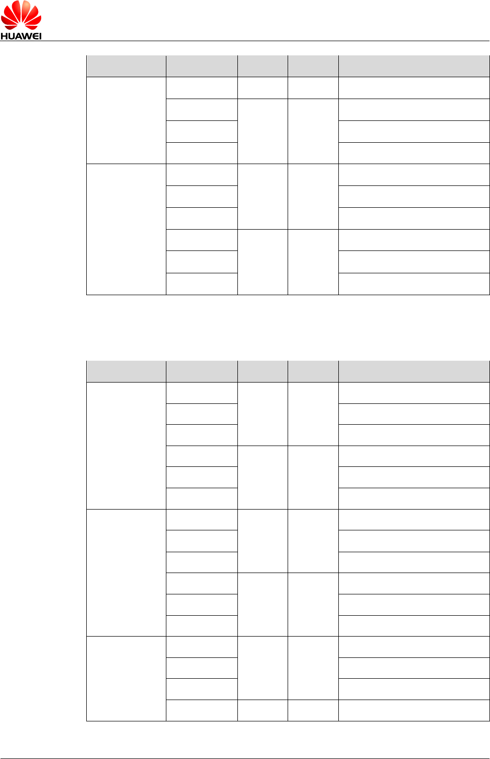
HUAWEI ME909s Series LTE LGA Module
Hardware Guide
Electrical and Reliability Features
Issue 04 (2016-12-21)
Huawei Proprietary and Confidential
Copyright © Huawei Technologies Co., Ltd.
73
Description
Test Value
Units
PCL
Configuration
390
4 Up/1 Down
121
mA
15
1 Up/1 Down
157
2 Up/1 Down
238
4 Up/1 Down
EDGE 1800
161
mA
2
1 Up/1 Down
225
2 Up/1 Down
295
4 Up/1 Down
108
mA
10
1 Up/1 Down
136
2 Up/1 Down
194
4 Up/1 Down
Table 5-11 Averaged DC power consumption of ME909s-120 LGA module
(GPRS/EDGE)
Description
Test Value
Units
PCL
Configuration
GPRS 850
307
mA
5
1 Up/1 Down
455
2 Up/1 Down
625
4 Up/1 Down
172
mA
10
1 Up/1 Down
258
2 Up/1 Down
435
4 Up/1 Down
GPRS 900
315
mA
5
1 Up/1 Down
445
2 Up/1 Down
615
4 Up/1 Down
175
mA
10
1 Up/1 Down
257
2 Up/1 Down
430
4 Up/1 Down
GPRS 1800
210
mA
0
1 Up/1 Down
285
2 Up/1 Down
380
4 Up/1 Down
112
mA
10
1 Up/1 Down
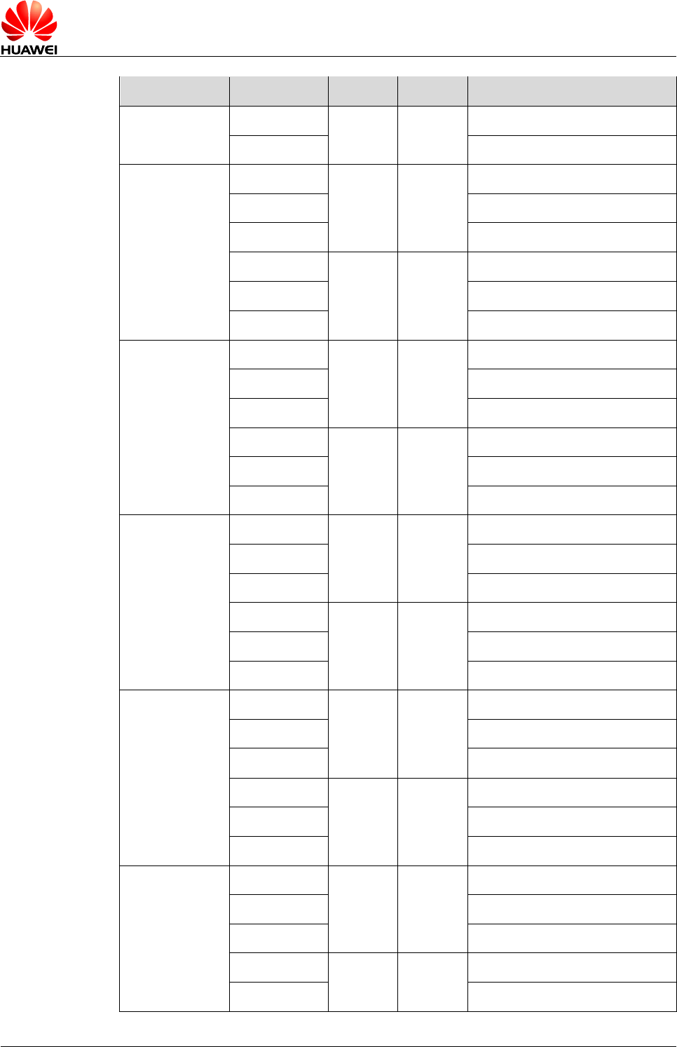
HUAWEI ME909s Series LTE LGA Module
Hardware Guide
Electrical and Reliability Features
Issue 04 (2016-12-21)
Huawei Proprietary and Confidential
Copyright © Huawei Technologies Co., Ltd.
74
Description
Test Value
Units
PCL
Configuration
145
2 Up/1 Down
195
4 Up/1 Down
GPRS 1900
230
mA
0
1 Up/1 Down
323
2 Up/1 Down
440
4 Up/1 Down
115
mA
10
1 Up/1 Down
145
2 Up/1 Down
205
4 Up/1 Down
EDGE 850
210
mA
8
1 Up/1 Down
295
2 Up/1 Down
387
4 Up/1 Down
125
mA
15
1 Up/1 Down
165
2 Up/1 Down
245
4 Up/1 Down
EDGE 900
205
mA
8
1 Up/1 Down
287
2 Up/1 Down
382
4 Up/1 Down
125
mA
15
1 Up/1 Down
165
2 Up/1 Down
245
4 Up/1 Down
EDGE 1800
170
mA
2
1 Up/1 Down
230
2 Up/1 Down
310
4 Up/1 Down
108
mA
10
1 Up/1 Down
135
2 Up/1 Down
195
4 Up/1 Down
EDGE 1900
187
mA
2
1 Up/1 Down
248
2 Up/1 Down
335
4 Up/1 Down
114
mA
10
1 Up/1 Down
145
2 Up/1 Down
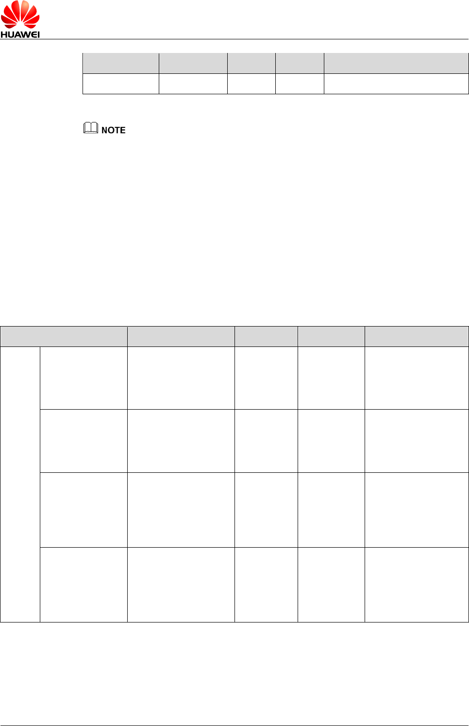
HUAWEI ME909s Series LTE LGA Module
Hardware Guide
Electrical and Reliability Features
Issue 04 (2016-12-21)
Huawei Proprietary and Confidential
Copyright © Huawei Technologies Co., Ltd.
75
Description
Test Value
Units
PCL
Configuration
205
4 Up/1 Down
- All power consumption test configuration can be referenced by GSM Association Official
Document TS.09: Battery Life Measurement and Current Consumption Technique.
- LTE test condition: 10/20 MHz bandwidth, QPSK, 1 RB when testing max. Tx power and full
RB when testing 0 dBm or 10 dBm.
- Test condition: For Max. Tx. power, see 4.4.2 Conducted Transmit Power, which are listed in
Table 4-5 and Table 4-6 , for Max. data throughput, see 2.2 Function Overview, which are
listed in Table 2-1 .
5.5 Reliability Features
Table 5-12 lists the test conditions and results of the reliability of the ME909s LGA
module.
Table 5-12 Test conditions and results of the reliability of the ME909s LGA module
Item
Test Condition
Standard
Sample size
Results
Stress
Low-temperature
storage
- Temperature: –40ºC
- Operation mode: no
power, no package
- Test duration: 24 h
JESD22-A1
19-C
3 pcs/group
Visual inspection: OK
Function test: OK
RF specification: OK
High-temperature
storage
- Temperature: 85ºC
- Operation mode: no
power, no package
- Test duration: 24 h
JESD22-A1
03-C
3 pcs/group
Visual inspection: OK
Function test: OK
RF specification: OK
Low-temperature
operating
- Temperature: –40ºC
- Operation mode:
working with service
connected
- Test duration: 24 h
IEC60068-2
-1
3 pcs/group
Visual inspection: OK
Function test: OK
RF specification: OK
High-temperature
operating
- Temperature: 85ºC
- Operation mode:
working with service
connected
- Test duration: 24 h
JESD22-A1
08-C
3 pcs/group
Visual inspection: OK
Function test: OK
RF specification: OK
HUAWEI ME909s Series LTE LGA Module
Hardware Guide
Electrical and Reliability Features
Issue 04 (2016-12-21)
Huawei Proprietary and Confidential
Copyright © Huawei Technologies Co., Ltd.
76
Item
Test Condition
Standard
Sample size
Results
Temperature
cycle operating
- High temperature:
85ºC
- Low temperature:
–40ºC
- Operation mode:
working with service
connected
- Test duration: 30
cycles;1 h+1 h/cycle
JESD22-A1
05-B
3pcs/group
Visual inspection: OK
Function test: OK
RF specification: OK
Damp heat
cycling
- High temperature:
55ºC
- Low temperature:
25ºC
- Humidity: 95%±3%
- Operation mode:
working with service
connected
- Test duration: 6
cycles; 12 h+12
h/cycle
JESD22-A1
01-B
3 pcs/group
Visual inspection: OK
Function test: OK
RF specification: OK
Thermal shock
- Low temperature:
–40ºC
- High temperature:
85ºC
- Temperature
change interval: <
30s
- Operation mode: no
power
- Test duration: 100
cycles; 15 min+15
min/cycle
JESD22-A1
06-B
3 pcs/group
Visual inspection: OK
Function test: OK
RF specification: OK
Salty fog test
- Temperature: 35°C
- Density of the NaCl
solution: 5%±1%
- Operation mode: no
power, no package
- Test duration:
Spraying interval: 8
h
Exposing period
after removing the
salty fog
environment: 16 h
JESD22-A1
07-B
3 pcs/group
Visual inspection: OK
Function test: OK
RF specification: OK
HUAWEI ME909s Series LTE LGA Module
Hardware Guide
Electrical and Reliability Features
Issue 04 (2016-12-21)
Huawei Proprietary and Confidential
Copyright © Huawei Technologies Co., Ltd.
77
Item
Test Condition
Standard
Sample size
Results
Sine vibration
- Frequency range: 5
Hz to 200 Hz
- Acceleration: 1
Grms
- Frequency scan
rate: 0.5 oct/min
- Operation mode:
working with service
connected
- Test duration: 3
axial directions. 2 h
for each axial
direction.
JESD22-B1
03-B
3 pcs/group
Visual inspection: OK
Function test: OK
RF specification: OK
Shock test
- Half-sine wave
shock
- Peak acceleration:
30 Grms
- Shock duration: 11
ms
- Operation mode:
working with service
connected
- Test duration: 6
axial directions. 3
shocks for each
axial direction.
JESD-B104
-C
3 pcs/group
Visual inspection: OK
Function test: OK
RF specification: OK
Drop test
- 0.8 m in height.
Drop the module on
the marble terrace
with one surface
facing downwards,
six surfaces should
be tested.
- Operation mode: no
power, no package
IEC60068-2
-32
3 pcs/group
Visual inspection: OK
Function test: OK
RF specification: OK
Life
High temperature
operating life
- Temperature: 85ºC
- Operation mode:
working with service
connected
- Test duration: 168 h,
336 h, 500 h, 1000 h
for inspection point
JESD22-A1
08-B
50 pcs/group
Visual inspection: OK
Function test: OK
RF specification: OK
HUAWEI ME909s Series LTE LGA Module
Hardware Guide
Electrical and Reliability Features
Issue 04 (2016-12-21)
Huawei Proprietary and Confidential
Copyright © Huawei Technologies Co., Ltd.
78
Item
Test Condition
Standard
Sample size
Results
High temperature
& high humidity
- High temperature:
85ºC
- Humidity: 85%
- Operation mode:
powered on and no
working
- Test duration: 168 h,
336 h, 500 h, 1000 h
for inspection point
JESD22-A1
10-B
50 pcs/group
Visual inspection: OK
Function test: OK
RF specification: OK
Temperature
cycle-Non
operating
- High temperature:
85ºC
- Low temperature:
–40ºC
- Temperature
change slope:
6ºC/min
- Operation mode: no
power
- Test duration: 168
cycle,
336 cycle, 500
cycle, 668cycle for
inspection point
JESD22-A1
04-C
50 pcs/group
Visual inspection: OK
Function test: OK
RF specification: OK
ESD
HBM (Human
Body Model)
- 1 kV (Class 1 B)
- Operation mode: no
power
JESD22-A1
14-D
3 pcs/group
Visual inspection: OK
Function test: OK
RF specification: OK
ESD with DVK (or
embedded in the
host)
- Contact Voltage: ±2
kV, ±4 kV
- Air Voltage: ±2 kV,
±4 kV, ±8 kV
- Operation mode:
working with service
connected
IEC61000-4
-2
2 pcs
Visual inspection: OK
Function test: OK
RF specification: OK
Groups ≥ 2
5.6 EMC and ESD Features
The following are the EMC design comments:
- Attention should be paid to static control in the manufacture, assembly, packaging,
handling and storage process to reduce electrostatic damage to HUAWEI
module.

HUAWEI ME909s Series LTE LGA Module
Hardware Guide
Electrical and Reliability Features
Issue 04 (2016-12-21)
Huawei Proprietary and Confidential
Copyright © Huawei Technologies Co., Ltd.
79
- RSE (Radiated Spurious Emission) may exceed the limit defined by EN301489 if
the antenna port is protected by TVS (Transient Voltage Suppressor), which is
resolved by making some adjustment on RF match circuit.
- TVS should be added on the USB port for ESD protection, and the parasitic
capacitance of TVS on D+/D- signal should be less than 2 pF. Common-mode
inductor should be added in parallel on D+/D- signal.
- TVS should be added on the USIM interface for ESD protection. The parasitic
capacitance of TVS on USIM signal should be less than 10 pF;
- Resistors in parallel and a 10nF capacitance should be added on RESIN_N and
POWER_ON_OFF signal to avoid shaking, and the distance between the
capacitor and the related pins should be less than 100 mil.
- A TVS should be added to the module power supply. It is recommended that the
TVS's Clamping Voltage (VCL) be smaller than 12 V and Peak Pulse Power (PPP)
at least 100 W.
- PCB routing should be V-type rather than T-type for TVS (Transient Voltage
Suppressor).
- An integrated ground plane is necessary for EMC design.
The following are the requirements of ESD environment control:
- The electrostatic discharge protected area (EPA) must have an ESD floor whose
surface resistance and system resistance are greater than 1 x 10⁴ Ω while less
than 1 x 10⁹ Ω.
- The EPA must have a sound ground system without loose ground wires, and the
ground resistance must be less than 4 Ω.
- The workbench for handling ESD sensitive components must be equipped with
common ground points, the wrist strap jack, and ESD pad. The resistance
between the jack and common ground point must be less than 4 Ω. The surface
resistance and system resistance of the ESD pad must be less than 1 x 10⁹ Ω.
- The EPA must use the ESD two-circuit wrist strap, and the wrist strap must be
connected to the dedicated jack. The crocodile clip must not be connected to the
ground.
- The ESD sensitive components, the processing equipment, test equipment, tools,
and devices must be connected to the ground properly. The indexes are as
follows:
− Hard ground resistance < 4 Ω
− 1 x 10⁵ Ω ≤ Soft ground resistance < 1 x 10⁹ Ω
− 1 x 10⁵ Ω ≤ ICT fixture soft ground resistance < 1 x 10¹¹ Ω
− The electronic screwdriver and electronic soldering iron can be easily oxidized.
Their ground resistance must be less than 20 Ω.
- The parts of the equipment, devices, and tools that touch the ESD sensitive
components and moving parts that are close to the ESD sensitive components
must be made of ESD materials and have sound ground connection. The parts
that are not made of ESD materials must be handled with ESD treatment, such
as painting the ESD coating or ionization treatment (check that the friction voltage
is less than 100 V).
- Key parts in the production equipment (parts that touch the ESD sensitive
components or parts that are within 30 cm away from the ESD sensitive
components), including the conveyor belt, conveyor chain, guide wheel, and SMT
nozzle, must all be made of ESD materials and be connected to the ground
properly (check that the friction voltage is less than 100 V).
HUAWEI ME909s Series LTE LGA Module
Hardware Guide
Electrical and Reliability Features
Issue 04 (2016-12-21)
Huawei Proprietary and Confidential
Copyright © Huawei Technologies Co., Ltd.
80
- Engineers that touch IC chips, boards, modules, and other ESD sensitive
components and assemblies must wear ESD wrist straps, ESD gloves, or ESD
finger cots properly. Engineers that sit when handling the components must all
wear ESD wrist straps.
- Noticeable ESD warning signs must be attached to the packages and placement
areas of ESD sensitive components and assemblies.
- Boards and IC chips must not be stacked randomly or be placed with other ESD
components.
- Effective shielding measures must be taken on the ESD sensitive materials that
are transported or stored outside the EPA.
HUAWEI ME909s LGA module does not include any protection against overvoltage.

HUAWEI ME909s Series LTE LGA Module
Hardware Guide
Mechanical Specifications
Issue 04 (2016-12-21)
Huawei Proprietary and Confidential
Copyright © Huawei Technologies Co., Ltd.
81
6 Mechanical Specifications
6.1 About This Chapter
This chapter describes the process design and mechanical specifications:
- Storage Requirement
- Moisture Sensitivity
- Dimensions
- Packaging
- Customer PCB Design
- Thermal Design Solution
- Assembly Processes
- Specification of Rework
6.2 Storage Requirement
The module must be stored and sealed properly in vacuum package under a
temperature below 40°C and the relative humidity less than 90% in order to ensure
the weldability within 12 months.
6.3 Moisture Sensitivity
- The moisture sensitivity is level 3.
- After unpacking, the module must be assembled within 168 hours under the
environmental conditions that the temperature is lower than 30°C and the relative
humidity is less than 60%. If the preceding conditions cannot be met, the module
needs to be baked according to the parameters specified in Table 6-1 .
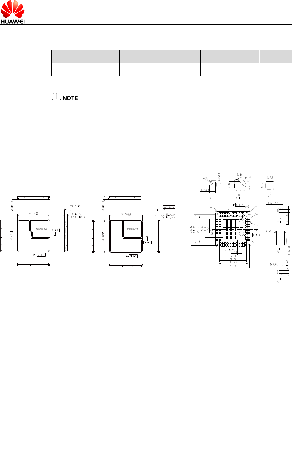
HUAWEI ME909s Series LTE LGA Module
Hardware Guide
Mechanical Specifications
Issue 04 (2016-12-21)
Huawei Proprietary and Confidential
Copyright © Huawei Technologies Co., Ltd.
82
Table 6-1 Baking parameters
Baking Temperature
Baking Condition
Baking Duration
Remarks
125°C ±5°C
Relative humidity ≤ 60%
8 hours
-
Moving, storing, and processing the product must comply with IPC/JEDEC J-STD-033.
6.4 Dimensions
Figure 6-1 shows the dimensions in details.
Figure 6-1 Dimensions (Unit: mm)
6.5 Packaging
HUAWEI LGA module uses five layers ESD pallet, anti-vibration foam and vacuum
packing into cartons. The tray specification complies with Jedec_Tray_DGuide4-10D.
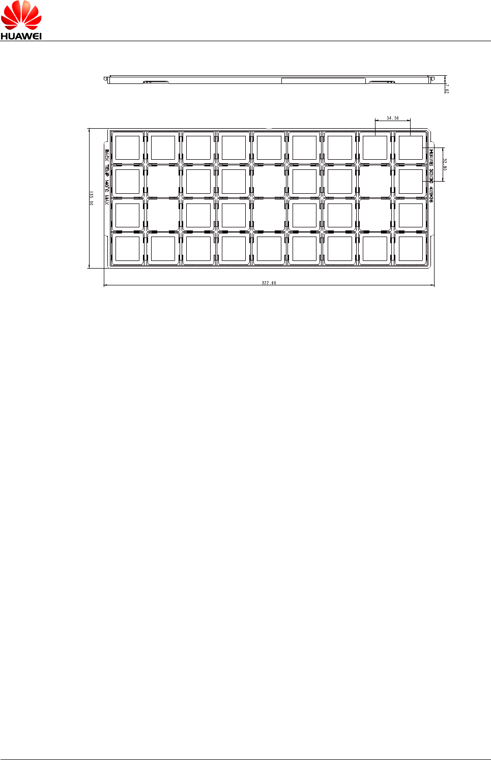
HUAWEI ME909s Series LTE LGA Module
Hardware Guide
Mechanical Specifications
Issue 04 (2016-12-21)
Huawei Proprietary and Confidential
Copyright © Huawei Technologies Co., Ltd.
83
Figure 6-2 ESD pallet (Unit: mm)
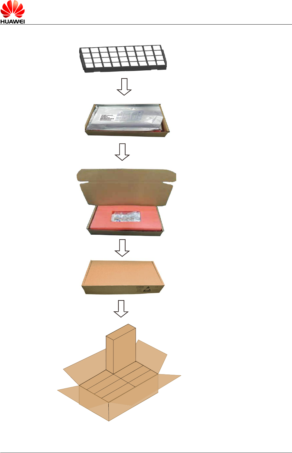
HUAWEI ME909s Series LTE LGA Module
Hardware Guide
Mechanical Specifications
Issue 04 (2016-12-21)
Huawei Proprietary and Confidential
Copyright © Huawei Technologies Co., Ltd.
84
Figure 6-3 The packaging
Module quantity per tray:
4 x 9 = 36 pcs/tray
Use vacuum packages;
five trays per carton;
module quantity per carton:
5 x 36 = 180 pcs/carton.
8 middle cartons per large carton;
Module quantity per large carton:
180 x 8 = 1440 pcs/carton.
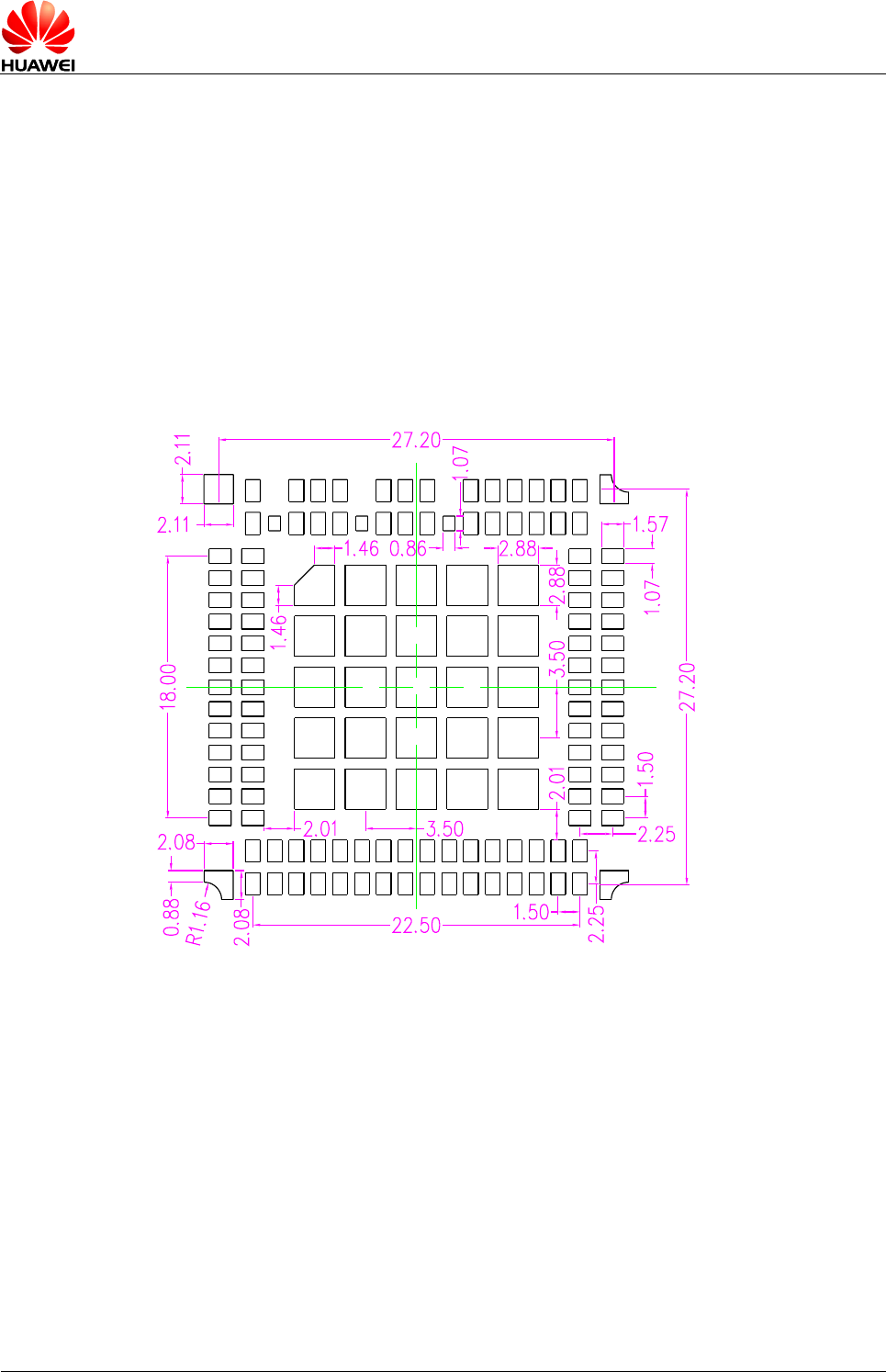
HUAWEI ME909s Series LTE LGA Module
Hardware Guide
Mechanical Specifications
Issue 04 (2016-12-21)
Huawei Proprietary and Confidential
Copyright © Huawei Technologies Co., Ltd.
85
6.6 Customer PCB Design
6.6.1 PCB Surface Finish
The PCB surface finish recommended is Electroless Nickel, immersion Gold (ENIG).
Organic Solderability Preservative (OSP) may also be used, ENIG preferred.
6.6.2 PCB Pad Design
To achieve assembly yields and solder joints of high reliability, it is recommended that
the PCB pad size be designed as follows:
Figure 6-4 ME909s LGA module Footprint design (Unit: mm)
6.6.3 Solder Mask
NSMD is recommended. In addition, the solder mask of the NSMD (Non-solder Mask
Defined) pad design is larger than the pad so the reliability of the solder joint can be
improved.
The solder mask must be 100 µm–150 µm larger than the pad, that is, the single side
of the solder mask must be 50 µm–75 µm larger than the pad. The specific size
depends on the processing capability of the PCB manufacturer.
6.6.4 Requirements on PCB Layout
- To reduce deformation, a thickness of at least 1.0 mm is recommended.
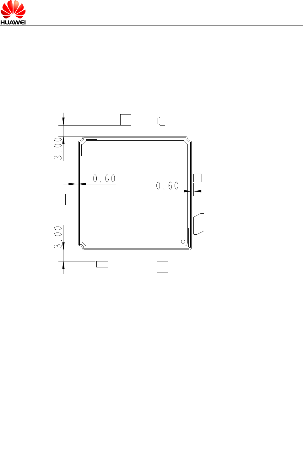
HUAWEI ME909s Series LTE LGA Module
Hardware Guide
Mechanical Specifications
Issue 04 (2016-12-21)
Huawei Proprietary and Confidential
Copyright © Huawei Technologies Co., Ltd.
86
- Other devices must be located more than 3 mm (5 mm recommended) away from
the two parallel sides of the LGA module (rework requirement), and other sides
with 0.6 mm. The minimum distance between the LGA module and the PCB edge
is 0.3 mm.
- When the PCB layout is double sided, the module must be placed on the second
side for assembly; so as to avoid module dropped from PCB or component
(located in module) re-melding defects caused by uneven weight.
Figure 6-5 PCB Layout (Unit: mm)
6.7 Thermal Design Solution
When the module works in the maximum power condition, the module has high power
consumption (for details, see Power Consumption). To improve the module reliability
and stability, focus on the thermal design of the device to speed up heat dissipation.
For thermal characteristics of the ME909s LGA module, you can refer to Operating
and Storage Temperatures.
Take the following heat dissipation measures:
- The copper size on the PCB should be 70 mm x 70 mm or larger.
- All copper ground layers of the PCB must be connected to each other through
via-holes.
- Increase the quantity of the PCB ground planes.
- The ground planes should be as continuous as possible.
- If a fan is deployed, place the module at the cold air inlet.
- Use heat sink, thermal conductive material and product enclosure to enhance the
heat dissipation of the module.
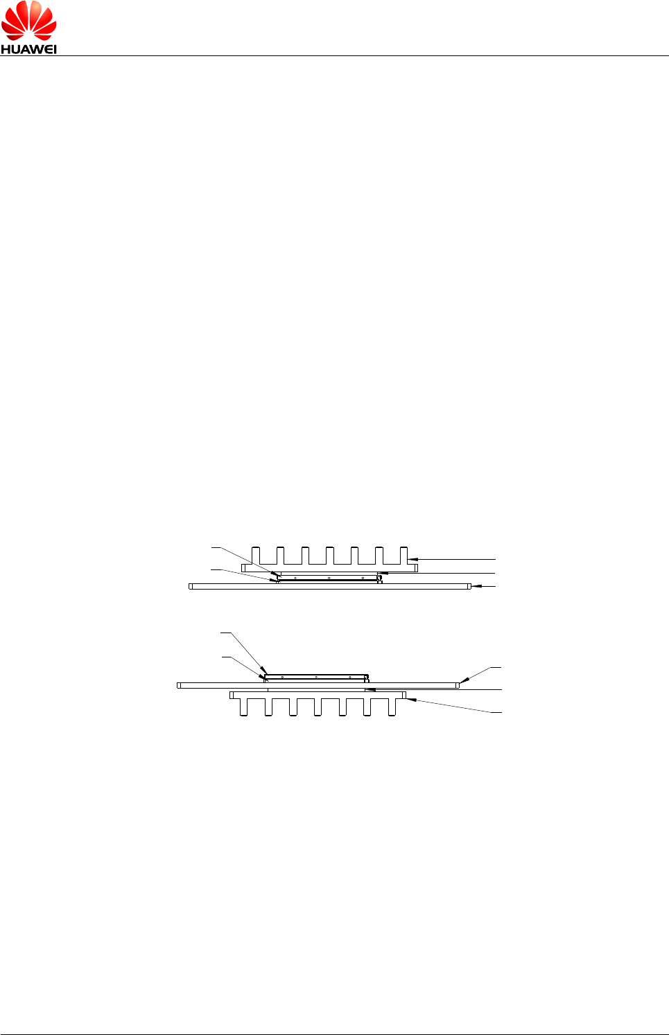
HUAWEI ME909s Series LTE LGA Module
Hardware Guide
Mechanical Specifications
Issue 04 (2016-12-21)
Huawei Proprietary and Confidential
Copyright © Huawei Technologies Co., Ltd.
87
− Use anodized heat sink on the shielding case or the customer PCB on bottom
side for optimal heat dissipation. The recommended heat sink dimensions are
70 mm x 70 mm x1 mm or larger.
− The material of the heat sink should adopt the higher thermal conductivity
metallic materials, e.g. Al or Cu.
− The recommended thermal conductivity of the thermal conductive material is
1.0 W/m-k or higher (recommended manufacturers: Laird or Bergquist).
− Conductive material should obey the following rule: after the heat sink is
fastened to the shielding case, the compression amount of the thermal
conductive material accounts for 15% to 30% of the thermal conductive
material size.
− Conductive material should be as thin as possible.
− The recommended material of the enclosure is metallic materials, especially
you can add pin fin on the enclosure surface.
− If the heat sink is installed above the shielding case, you should attach the
thermal conductive material between the shielding case and the heat sink; if
the heat sink is installed below the bottom side of the customer PCB, you
should attach the thermal conductive material between the customer PCB and
the heat sink, as shown in Figure 6-6 and Figure 6-7 . Preferably, we
recommend the heat sink be installed below the bottom side of the customer
PCB.
− Use more pin fins to enlarge heat dissipation area.
Figure 6-6 Adding heat sink to the module for optimal heat dissipation
Module PCB Heat sink
Conductive material
Customer PCB
Module PCB
Heat sink
Conductive material
Customer PCB
Shielding case
Shielding case
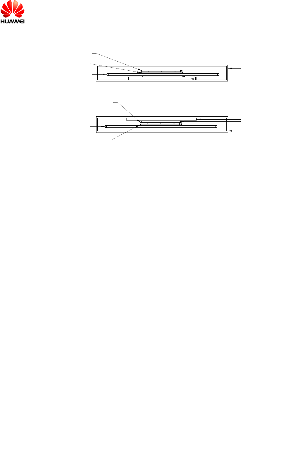
HUAWEI ME909s Series LTE LGA Module
Hardware Guide
Mechanical Specifications
Issue 04 (2016-12-21)
Huawei Proprietary and Confidential
Copyright © Huawei Technologies Co., Ltd.
88
Figure 6-7 Adding enclosure to enhance the heat dissipation of the module
Module PCB
Heat sink
Conductive material
Customer PCB Enclosure
Shielding case
Heat sink
Conductive material
Customer PCB Enclosure
Module PCB
Shielding case
6.8 Assembly Processes
6.8.1 General Description of Assembly Processes
- Tray modules are required at SMT lines, because LGA modules are placed on
ESD pallets.
- Reflow ovens with at least seven temperature zones are recommended.
- Use reflow ovens or rework stations for soldering, because LGA modules have
large solder pads and cannot be soldered manually.
6.8.2 Stencil Design
It is recommended that the stencil for the LGA module be 0.15 mm in thickness. For
the stencil design, see the following figure:
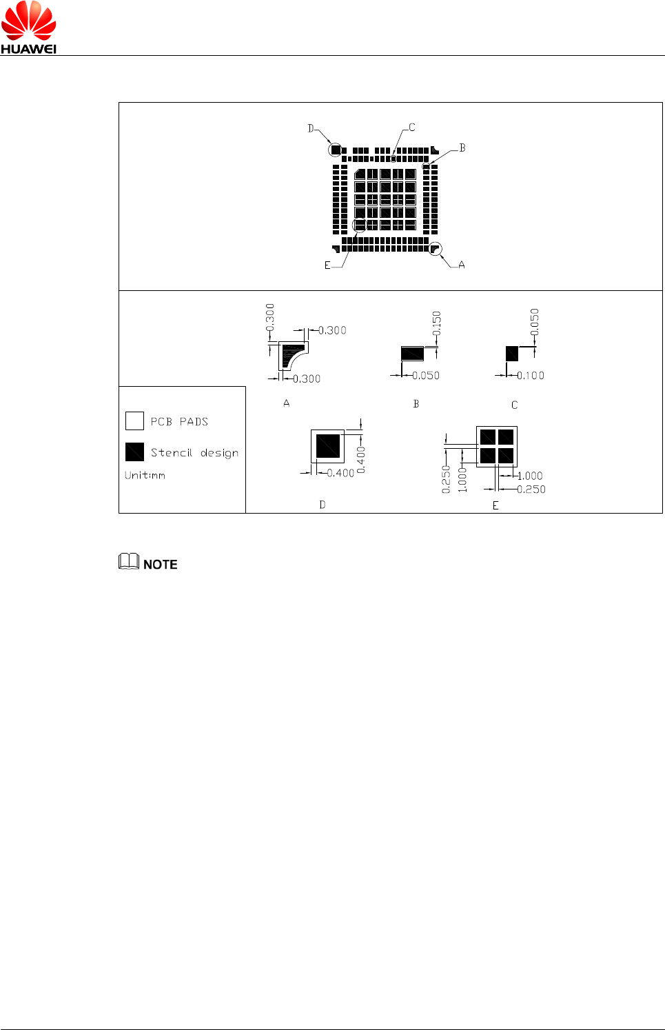
HUAWEI ME909s Series LTE LGA Module
Hardware Guide
Mechanical Specifications
Issue 04 (2016-12-21)
Huawei Proprietary and Confidential
Copyright © Huawei Technologies Co., Ltd.
89
Figure 6-8 Recommended stencil design of LGA module (Unit: mm)
The stencil design has been qualified for HUAWEI motherboard assembly, customers can
adjust the parameters by their motherboard design and process situation to assure LGA
soldering quality and no defect.
6.8.3 Reflow Profile
The LGA module must be reflowed on the top side of the customer's development
board. For the soldering temperature of the LGA module, see the following figure.
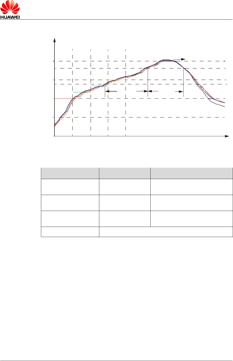
HUAWEI ME909s Series LTE LGA Module
Hardware Guide
Mechanical Specifications
Issue 04 (2016-12-21)
Huawei Proprietary and Confidential
Copyright © Huawei Technologies Co., Ltd.
90
Figure 6-9 Reflow profile
240
300
180
217
165
120
60
0s
°C
60s~100s 45s~80s
235°C<Tmax<245°C
Table 6-2 Reflow parameters
Temperature Zone
Time
Key Parameter
Preheat zone
(40°C–165°C)
-
Heating rate: 0.5°C/s–2°C/s
Soak zone
(165°C –217°C)
(t1–t2): 60s–100s
-
Reflow zone (> 217°C)
(t3–t4): 45s–80s
Peak reflow temperature:
235°C –245°C
Cooling zone
Cooling rate: 2°C/s ≤ Slope ≤ 5°C/s
6.9 Specification of Rework
6.9.1 Process of Rework
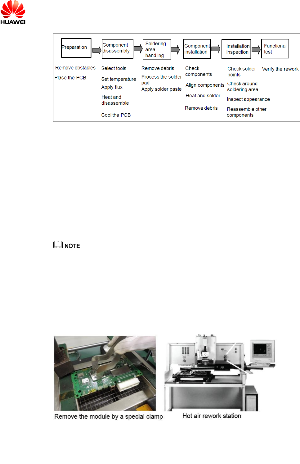
HUAWEI ME909s Series LTE LGA Module
Hardware Guide
Mechanical Specifications
Issue 04 (2016-12-21)
Huawei Proprietary and Confidential
Copyright © Huawei Technologies Co., Ltd.
91
6.9.2 Preparations of Rework
- Remove barrier or devices that can’t stand high temperature before rework.
- If the device to be reworked is beyond the storage period, bake the device
according to Table 6-1 .
6.9.3 Removing of the Module
The solder is molten and reflowed through heating during the module removing
process. The heating rate must be quick but controllable in order to melt all the solder
joints simultaneously. Pay attention to protect the module, PCB, neighboring devices,
and their solder joints against heating or mechanical damages.
- The LGA module has many solder pads and the pads are large. Therefore, common
soldering irons and heat guns cannot be used in the rework. Rework must be done using
either infrared heating rework stations or hot air rework stations. Infrared heating rework
stations are preferred, because they can heat components without touching them. In
addition, infrared heating rework stations produce less solder debris and less impact on
modules, while hot air rework stations may cause shift of other components not to be
reworked.
- You must not reuse the module after disassembly from PCB during rework.
- It is proposed that a special clamp is used to remove the module.
Figure 6-10 Equipment used for rework
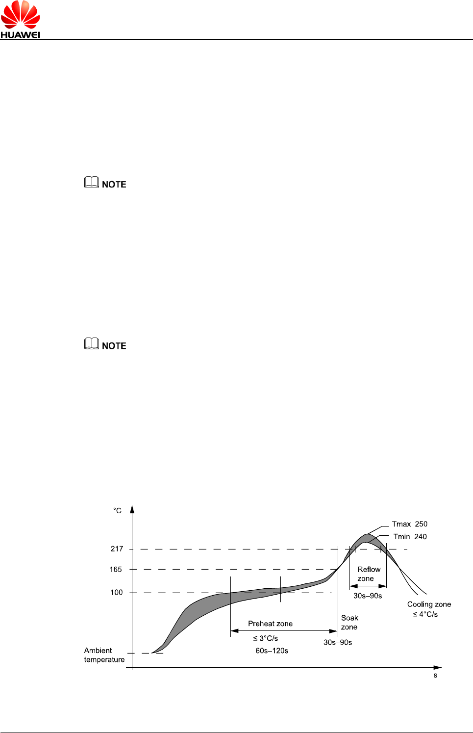
HUAWEI ME909s Series LTE LGA Module
Hardware Guide
Mechanical Specifications
Issue 04 (2016-12-21)
Huawei Proprietary and Confidential
Copyright © Huawei Technologies Co., Ltd.
92
6.9.4 Welding Area Treatment
Step 1 Remove the old solder by using a soldering iron and solder braid that can wet the
solder.
Step 2 Clean the pad and remove the flux residuals.
Step 3 Solder pre-filling: Before the module is installed on a board, apply some solder paste
to the pad of the module by using the rework fixture and stencil or apply some solder
paste to the pad on the PCB by using a rework stencil.
It is recommended that a fixture and a mini-stencil be made to apply the solder paste in the
rework.
6.9.5 Module Installation
Install the module precisely on the motherboard and ensure the right installation
direction of the module and the reliability of the electrical connection with the PCB. It is
recommended that the module be preheated in order to ensure that the temperature
of all parts to be soldered is uniform during the reflow process. The solder quickly
reflows upon heating so the parts are soldered reliably. The solder joints undergo
proper reflow duration at a preset temperature to form a favorable Inter-metallic
Compound (IMC).
- It is recommended that a special clamp be used to pick the module when the module is
installed on the pad after applied with some solder.
- A special rework device must be used for the rework.
6.9.6 Specifications of Rework
Temperature parameter of rework: for either the removing or welding of the module,
the heating rate during the rework must be equal to or smaller than 3°C/s, and the
peak temperature between 240°C–250°C. The following parameters are
recommended during the rework.
Figure 6-11 Temperature graph of rework
HUAWEI ME909s Series LTE LGA Module
Hardware Guide
Certifications
Issue 04 (2016-12-21)
Huawei Proprietary and Confidential
Copyright © Huawei Technologies Co., Ltd.
93
7 Certifications
7.1 About This Chapter
This chapter gives a general description of certifications of the ME909s LGA module.
7.2 Certifications
Figure 7-1 shows certifications the ME909s LGA module have been implemented. For more
demands, please contact us for more details about this information.
Figure 7-1 Product Certifications of ME909s LGA module
Certification
Model name
ME909s -821
ME909s -120
CE
-
√
RoHS
√
√
CCC
√
-
GCF
-
√
WEEE
√
√

HUAWEI ME909s Series LTE LGA Module
Hardware Guide
Safety Information
Issue 04 (2016-12-21)
Huawei Proprietary and Confidential
Copyright © Huawei Technologies Co., Ltd.
94
8 Safety Information
8.1 About This Chapter
Read the safety information carefully to ensure the correct and safe use of your
wireless device. Applicable safety information must be observed.
- Interference
- Medical Device
- Area with Inflammables and Explosives
- Traffic Security
- Airline Security
- Safety of Children
- Environment Protection
- WEEE Approval
- RoHS Approval
- Laws and Regulations Observance
- Care and Maintenance
- Emergency Call
- Regulatory Information
8.2 Interference
Power off your wireless device if using the device is prohibited. Do not use the
wireless device when it causes danger or interference with electric devices.
8.3 Medical Device
- Power off your wireless device and follow the rules and regulations set forth by
the hospitals and health care facilities.
- Some wireless devices may affect the performance of the hearing aids. For any
such problems, consult your service provider.

HUAWEI ME909s Series LTE LGA Module
Hardware Guide
Safety Information
Issue 04 (2016-12-21)
Huawei Proprietary and Confidential
Copyright © Huawei Technologies Co., Ltd.
95
- Pacemaker manufacturers recommend that a minimum distance of 15 cm be
maintained between the wireless device and a pacemaker to prevent potential
interference with the pacemaker. If you are using an electronic medical device,
consult the doctor or device manufacturer to confirm whether the radio wave
affects the operation of this device.
8.4 Area with Inflammables and Explosives
To prevent explosions and fires in areas that are stored with inflammable and
explosive devices, power off your wireless device and observe the rules. Areas stored
with inflammables and explosives include but are not limited to the following:
- Gas station
- Fuel depot (such as the bunk below the deck of a ship)
- Container/Vehicle for storing or transporting fuels or chemical products
- Area where the air contains chemical substances and particles (such as granule,
dust, or metal powder)
- Area indicated with the "Explosives" sign
- Area indicated with the "Power off bi-direction wireless equipment" sign
- Area where you are generally suggested to stop the engine of a vehicle
8.5 Traffic Security
- Observe local laws and regulations while using the wireless device. To prevent
accidents, do not use your wireless device while driving.
- RF signals may affect electronic systems of motor vehicles. For more information,
consult the vehicle manufacturer.
- In a motor vehicle, do not place the wireless device over the air bag or in the air
bag deployment area. Otherwise, the wireless device may hurt you owing to the
strong force when the air bag inflates.
8.6 Airline Security
Observe the rules and regulations of airline companies. When boarding or
approaching a plane, power off your wireless device. Otherwise, the radio signal of
the wireless device may interfere with the plane control signals.
8.7 Safety of Children
Do not allow children to use the wireless device without guidance. Small and sharp
components of the wireless device may cause danger to children or cause suffocation
if children swallow the components.

HUAWEI ME909s Series LTE LGA Module
Hardware Guide
Safety Information
Issue 04 (2016-12-21)
Huawei Proprietary and Confidential
Copyright © Huawei Technologies Co., Ltd.
96
8.8 Environment Protection
Observe the local regulations regarding the disposal of your packaging materials,
used wireless device and accessories, and promote their recycling.
8.9 WEEE Approval
The wireless device is in compliance with the essential requirements and other
relevant provisions of the Waste Electrical and Electronic Equipment Directive
2012/19/EU (WEEE Directive).
8.10 RoHS Approval
The wireless device is in compliance with the restriction of the use of certain
hazardous substances in electrical and electronic equipment Directive 2011/65/EU
(RoHS Directive).
8.11 Laws and Regulations Observance
Observe laws and regulations when using your wireless device. Respect the privacy
and legal rights of the others.
8.12 Care and Maintenance
It is normal that your wireless device gets hot when you use or charge it. Before you
clean or maintain the wireless device, stop all applications and power off the wireless
device.
- Use your wireless device and accessories with care and in clean environment.
Keep the wireless device from a fire or a lit cigarette.
- Protect your wireless device and accessories from water and vapour and keep
them dry.
- Do not drop, throw or bend your wireless device.
- Clean your wireless device with a piece of damp and soft antistatic cloth. Do not
use any chemical agents (such as alcohol and benzene), chemical detergent, or
powder to clean it.
- Do not leave your wireless device and accessories in a place with a considerably
low or high temperature.
- Use only accessories of the wireless device approved by the manufacture.
Contact the authorized service center for any abnormity of the wireless device or
accessories.
- Do not dismantle the wireless device or accessories. Otherwise, the wireless
device and accessories are not covered by the warranty.
- The device should be installed and operated with a minimum distance of 20 cm
between the radiator and your body.
HUAWEI ME909s Series LTE LGA Module
Hardware Guide
Safety Information
Issue 04 (2016-12-21)
Huawei Proprietary and Confidential
Copyright © Huawei Technologies Co., Ltd.
97
8.13 Emergency Call
This wireless device functions through receiving and transmitting radio signals.
Therefore, the connection cannot be guaranteed in all conditions. In an emergency,
you should not rely solely on the wireless device for essential communications.
8.14 Regulatory Information
The following approvals and notices apply in specific regions as noted.
8.14.1 CE Approval (European Union)
The wireless device is approved to be used in the member states of the EU. The
wireless device is in compliance with the essential requirements and other relevant
provisions of the Radio and Telecommunications Terminal Equipment Directive
1999/5/EC (R&TTE Directive).
HUAWEI ME909s Series LTE LGA Module
Hardware Guide
Appendix A Circuit of Typical Interface
Issue 04 (2016-12-21)
Huawei Proprietary and Confidential
Copyright © Huawei Technologies Co., Ltd.
98
9 Appendix A Circuit of Typical Interface
HUAWEI MU709 Series HSPA+ LGA Module
Hardware Guide
Appendix A Circuit of Typical Interface
Issue 06 (2015-11-30)
Huawei Proprietary and Confidential
Copyright ©Huawei Technologies Co.,Ltd.
81
R330
**10K
U304
0HPA00615DRVR
5
3
6
4 7
2
1
OUT
ILIM
EN
IN
FAULT
GND1
R33130K
L303 2.2uF
2
1
R328 1MEG
C322
1uF
C321
100nF
C320
4.7uF
C308
100nF
C307
100nF
C306
22uF
C305
150uF 1
C318
22uF
C316
100nF
C304
150uF 1
C319
22uF
C317
1uF
R327180K
R32620K R325
75K
U301
0
RT8015AGQW
SHDN/RT
GND1
LX1
LX2
PGNDPVDD1
PVDD2
GND2
COMP
VDD
FB
C313220pF
C310
22pF
C303
150uF 1
C302
150uF 1
C301
150uF 1
R324
47K
U302
LGA120H-3030A
145
144
143
142
141
140
139
138
137
136
135
134
133
132
131
130
129
128
127
124
123
122
121
116
114
112
110
108
106
59
58
57
56
54
53
52
50
GND
48
NOT used
49
GND
GND
NOT used
GND
GND
NOT used
GND
GND
GND
GND
GND
GND
GND
GND
GND
GND
GND
GND
GND 125
GND 126
GND
GND
GND
GND
GND
GND
GND
GND
GND
GND
GND
GND
GND
GND
GND
GND
GND
GND
GND
ME909s_MISC
5V-P-3
C358
USIM_CLK
USIM_DATA
USIM_RESET
USIM_DET
USIM_VCC
U302
LGA120H-3030A
71
11
35
33
92
31
32
13
12
84
86
85
1
4
2
3
76
78
74
77
79
73
75
80
98
99
65
64
63
62
34
88
70
89
90
66
10
9
68
69
67
5
7
6
8
120
119
118
117
83
82
38
39
40
41
91
101
22
21
20
19
18
27
26
25
24
23
36
30
72
87
42
93
61
60
94
95
113
109
105
55
51
46
45
44
43
29
28
15
14
16
17
97
96
104
102
100
37
47
103
81
111
115
107 MAIN_ANT
AUX_ANT
POWER_ON_OFF
RESIN_N
ADC_1
ADC_2
RESERVED
RESERVED
RESERVED
SLEEP_STATUS
GPIO1
UART2_RX
UART2_TX
RESERVED
RESERVED
RESERVED
RESERVED
RESERVED
GPIO2
GPIO3
GPIO4/USIM Switch
GPIO5
GPIO6
GPIO7/Jamming Detection
RESERVED
UART0_DSR
UART0_DTR
UART0_DCD
RESERVED
RESERVED
JTAG_RTCK
JTAG_TCK
JTAG_TDI
JTAG_TDO
JTAG_TMS
JTAG_TRST_N
NC
NC
RESERVED
NC
NC
NC
NC
NC
NC
NC
NC
NC
NC
PCM_CLK
PCM_DIN
PCM_DOUT
PCM_SYNC
SD_CLK
SD_CMD
SD_DATA0
SD_DATA1
SD_DATA2
SD_DATA3
USIM_CLK
USIM_DATA
USIM_RESET
USIM_VCC
RESERVED
RESERVED
RESERVED
RESERVED
UART0_RING
UART0_CTS
UART0_RTS
UART0_RX
UART0_TX
RESERVED
RESERVED
USB_DM
USB_DP
NC
VBAT
VBAT
RESERVED
RESERVED
WAKEUP_IN
WAKEUP_OUT
ME909s_MISC
C370
1uF
C360
33pF
C361
33pF 33pF
D310
SMF05CTC
61
3 4
2 5
C363
33pF
J301
WL629D3_T01_TR_A
1
2
3
4
5
6
P6
P5
P4
P3
P2
P1
C362
100nF
C379
Note:"**" means that this component is not welded, but need to reserve component solder pad.
RESERVED
RESERVED
RESERVED
RESERVED
RESERVED
RESERVED
LED_MODE
These are impedance matching
circuit, the specific capacitance
and inductance value needs to
be adjusted, based on the
characteristic impedance of
the practical PCB.
RV301
RV302
R301 0
R302 0
C353
**6.8pF
**6.8pF C354
C357 **2.2pF
C353 and C354 are ready for dealing with filter differentia
l mode interference and C357 is ready for dealing with
filter common mode interference.You can choose
the value of the C353, C354 and C357 according to the actual
PCB which is integrated 30mm×30mm LGA Module.
L320
C350
220uF
1
C351
220uF
1
C352**220uF
1
C355220uF
1
C354220uF
1
C356
C357
C358
33pF
10uF
100nF
R117
**2.2K Q109
BC847ALT1
**NPN-BEC
E2 3
B1
C
**10KR138
VCC_EXT1 WAKEUP_IN_TO_MODULE
WAKEUP_IN_TO_MODULE
WAKEUP_IN_FROM_HOST
Note: Pin 49, pin 53 and pin 57 do not
have pad in ME909s module.
0 Ω
0 Ω
0 Ω
0 Ω
b
c
e
R341
R342
R343 R344
R345 1K
0.47K
R340
VBAT
D311
NC
RV303
C372
C366
L310
L313
L314
L311
SMA6251A1_060_20GHT50GH_50
1
52 3 4
**33n
**33n
**33n **33n
2 5
J302
C371
SMA6251A1_060_20GHT50GH_50
1C365
J303
22pF
22pF
22pF 22pF
USIM_DET
3 4
2
2
2
2
2
RESERVED
RESERVED
RESERVED
RESERVED
RESERVED
NC
RESERVED
Test point1
Test point2
RESERVED
RESERVED
VCC_EXT1
RESERVED
SD_VCC
2
2
2
2
2
33pF
C123
VCC_EXT1
HUAWEI ME909s Series LTE LGA Module
Hardware Guide
Appendix B Acronyms and
Abbreviations
Issue 04 (2016-12-21)
Huawei Proprietary and Confidential
Copyright © Huawei Technologies Co., Ltd.
99
10 Appendix B Acronyms and
Abbreviations
Acronym or Abbreviation
Expansion
3GPP
Third Generation Partnership Project
8PSK
8 Phase Shift Keying
AP
Access Point
AUX
Auxiliary
BER
Bit Error Rate
BIOS
Basic Input Output System
CCC
China Compulsory Certification
CE
European Conformity
CMOS
Complementary Metal Oxide Semiconductor
CSD
Circuit Switched Data
DC
Direct Current
DCE
Data Communication Equipment
DL
Down Link
DMA
Direct Memory Access
DTE
Data Terminal Equipment
EDGE
Enhanced Data Rate for GSM Evolution
EIA
Electronic Industries Association
EMC
Electromagnetic Compatibility
ESD
Electrostatic Discharge
EU
European Union
HUAWEI ME909s Series LTE LGA Module
Hardware Guide
Appendix B Acronyms and
Abbreviations
Issue 04 (2016-12-21)
Huawei Proprietary and Confidential
Copyright © Huawei Technologies Co., Ltd.
100
Acronym or Abbreviation
Expansion
FCC
Federal Communications Commission
GMSK
Gaussian Minimum Shift Keying
GPIO
General-purpose I/O
GPRS
General Packet Radio Service
GSM
Global System for Mobile Communication
HBM
Human Body Model
HSDPA
High-Speed Downlink Packet Access
HSPA
Enhanced High Speed Packet Access
HSUPA
High Speed Up-link Packet Access
IMC
Inter-metallic Compound
ISO
International Standards Organization
JTAG
Joint Test Action Group
LED
Light-Emitting Diode
LGA
Land Grid Array
MO
Mobile Originated
MT
Mobile Terminated
NC
Not Connected
NSMD
Non-solder Mask Defined
PCB
Printed Circuit Board
PCM
Pulse Code Modulation
PDU
Protocol Data Unit
PMU
Power Management Unit
PID
Product Identity
RF
Radio Frequency
RoHS
Restriction of the Use of Certain Hazardous
Substances
SMS
Short Message Service
TIS
Total Isotropic Sensitivity
TVS
Transient Voltage Suppressor
UART
Universal Asynchronous Receiver-Transmitter
UL
Up Link
HUAWEI ME909s Series LTE LGA Module
Hardware Guide
Appendix B Acronyms and
Abbreviations
Issue 04 (2016-12-21)
Huawei Proprietary and Confidential
Copyright © Huawei Technologies Co., Ltd.
101
Acronym or Abbreviation
Expansion
UMTS
Universal Mobile Telecommunications System
USB
Universal Serial Bus
USIM
Universal Subscriber Identity Module
VIP
Vendor Identity
VSWR
Voltage Standing Wave Ratio
WEEE
Waste Electrical and Electronic Equipment
WCDMA
Wideband Code Division Multiple Access
WWAN
Wireless Wide Area Network
LTE
Long Term Evolution
