Huawei MU739 HSPA LGA Module Hardware Guide (V100R001 11, English)
HUAWEI MU739 HSPA+ LGA Module Hardware Guide-(V100R001_11, English)
2015-10-09
User Manual: Huawei
Open the PDF directly: View PDF ![]() .
.
Page Count: 80
- Revision History
- 1 Introduction
- 2 Overall Description
- 3 Description of the Application Interfaces
- 3.1 About This Chapter
- 3.2 LGA Interface
- 3.3 Power Interface
- 3.4 Signal Control Interface
- 3.5 USB Interface
- 3.6 USIM Card Interface
- 3.7 Audio Interface
- 3.8 JTAG Interface
- 3.9 RF Antenna Interface
- 3.10 Reserved Interface
- 3.11 NC Interface
- 4 RF Specifications
- 5 Electrical and Reliability Features
- 6 Process Design
- 6.1 About This Chapter
- 6.2 Storage Requirement
- 6.3 Moisture Sensitivity
- 6.4 Dimensions
- 6.5 Packaging
- 6.6 Label
- 6.7 Customer PCB Design
- 6.8 Thermal Design Solution
- 6.9 Assembly Processes
- 6.10 Specification of Rework
- 6.10.1 Process of Rework
- 6.10.2 Preparations of Rework
- 6.10.3 Removing the Module
- 6.10.4 Welding Area Treatmtent
- Step 1 Remove the old solder by using a soldering iron and solder braid that can wet the solder.
- Step 2 Clean the pad and remove the flux residuals.
- Step 3 Solder pre-filling: Before the module is installed on a board, apply some solder paste to the pad of the module by using the rework fixture and stencil or apply some solder paste to the pad on the PCB by using a rework stencil.
- 6.10.5 Module Installation
- 6.10.6 Specifications of Rework
- 7 Certifications
- 8 Safety Information
- 8.1 Interference
- 8.2 Medical Device
- 8.3 Area with Inflammables and Explosives
- 8.4 Traffic Security
- 8.5 Airline Security
- 8.6 Safety of Children
- 8.7 Environment Protection
- 8.8 WEEE Approval
- 8.9 RoHS Approval
- 8.10 Laws and Regulations Observance
- 8.11 Care and Maintenance
- 8.12 Emergency Call
- 8.13 Regulatory Information
- 9 Appendix A Circuit of Typical Interface
- 10 Appendix B Acronyms and Abbreviations

HUAWEI MU739 HSPA+ LGA Module
Hardware Guide
Issue
11
Date
2015-10-08

Copyright © Huawei Technologies Co., Ltd. 2015. All rights reserved.
No part of this manual may be reproduced or transmitted in any form or by any means without prior written
consent of Huawei Technologies Co., Ltd. and its affiliates ("Huawei").
The product described in this manual may include copyrighted software of Huawei and possible licensors.
Customers shall not in any manner reproduce, distribute, modify, decompile, disassemble, decrypt, extract,
reverse engineer, lease, assign, or sublicense the said software, unless such restrictions are prohibited by
applicable laws or such actions are approved by respective copyright holders.
Trademarks and Permissions
, , and are trademarks or registered trademarks of Huawei Technologies Co., Ltd.
Other trademarks, product, service and company names mentioned may be the property of their respective
owners.
Notice
Some features of the product and its accessories described herein rely on the software installed, capacities
and settings of local network, and therefore may not be activated or may be limited by local network operators
or network service providers.
Thus, the descriptions herein may not exactly match the product or its accessories which you purchase.
Huawei reserves the right to change or modify any information or specifications contained in this manual
without prior notice and without any liability.
DISCLAIMER
ALL CONTENTS OF THIS MANUAL ARE PROVIDED “AS IS”. EXCEPT AS REQUIRED BY APPLICABLE
LAWS, NO WARRANTIES OF ANY KIND, EITHER EXPRESS OR IMPLIED, INCLUDING BUT NOT
LIMITED TO, THE IMPLIED WARRANTIES OF MERCHANTABILITY AND FITNESS FOR A PARTICULAR
PURPOSE, ARE MADE IN RELATION TO THE ACCURACY, RELIABILITY OR CONTENTS OF THIS
MANUAL.
TO THE MAXIMUM EXTENT PERMITTED BY APPLICABLE LAW, IN NO EVENT SHALL HUAWEI BE
LIABLE FOR ANY SPECIAL, INCIDENTAL, INDIRECT, OR CONSEQUENTIAL DAMAGES, OR LOSS OF
PROFITS, BUSINESS, REVENUE, DATA, GOODWILL SAVINGS OR ANTICIPATED SAVINGS
REGARDLESS OF WHETHER SUCH LOSSES ARE FORSEEABLE OR NOT.
THE MAXIMUM LIABILITY (THIS LIMITATION SHALL NOT APPLY TO LIABILITY FOR PERSONAL
INJURY TO THE EXTENT APPLICABLE LAW PROHIBITS SUCH A LIMITATION) OF HUAWEI ARISING
FROM THE USE OF THE PRODUCT DESCRIBED IN THIS MANUAL SHALL BE LIMITED TO THE
AMOUNT PAID BY CUSTOMERS FOR THE PURCHASE OF THIS PRODUCT.
Import and Export Regulations
Customers shall comply with all applicable export or import laws and regulations and be responsible to obtain
all necessary governmental permits and licenses in order to export, re-export or import the product mentioned
in this manual including the software and technical data therein.
Privacy Policy
To better understand how we protect your personal information, please see the privacy policy at
http://consumer.huawei.com/privacy-policy.
HUAWEI MU739 HSPA+ LGA Module
Hardware Guide
About This Document
Issue 11 (2015-10-08)
Huawei Proprietary and Confidential
Copyright © Huawei Technologies Co., Ltd.
3
About This Document
Revision History
Version
Date
Chapter
Descriptions
01
2011-12-21
Creation
02
2012-01-04
6
Updated Figure 6-1
03
2012-02-29
3
Updated USB_VBUS voltage range
9
Updated Appendix A Circuit of Typical
Interface
04
2012-07-17
3.9
Deleted General Purpose I/O Interface in issue
03
9
Updated Appendix A Circuit of Typical
Interface
05
2012-08-23
6
Added the process design
06
2013-05-08
4.5.2
Updated Table 4-3
4.6.1
Updated Antenna Design Indicators
4.6.3
Updated GSM/WCDMA Antenna
Requirements
7.2
Updated Table 7-1
7.3
Deleted Environmental Protection Certification
and Test
7.4
Deleted National Compulsory Certification
7.5
Deleted GCF and PTCRB
8.8
Updated WEEE Approval
8.9
Updated RoHS Approval
8.11
Updated Care and Maintenance
8.13
Deleted Specific Absorption Rate (SAR)
8.13
Updated Regulatory Information
07
2014-07-29
2.2
Updated Table 2-1 Features
HUAWEI MU739 HSPA+ LGA Module
Hardware Guide
About This Document
Issue 11 (2015-10-08)
Huawei Proprietary and Confidential
Copyright © Huawei Technologies Co., Ltd.
4
Version
Date
Chapter
Descriptions
2.3
Updated Figure 2-1 Circuit block diagram of
the MU739 module
2.4
Updated Figure 2-2 Application block diagram
of the MU739 module
3
Updated definitions of pins
4.2
Deleted 4.2 Antenna Installation Guidelines
4.4
Updated Table 4-2 MU739 conducted Rx
sensitivity (Unit: dBm) and Table 4-3 MU739
conducted Tx power (Unit: dBm)
4.5.4
Deleted 4.5.4 Radio Test Environment
5.4
Deleted 5.4 Electrical Features of Application
Interfaces
5.4.2
Updated 5.4.2 Power Consumption
5.5
Updated 5.5 Reliability Features
5.6
Updated 5.6 EMC and ESD Features
6.5
Updated 6.5 Packaging
6.6
Updated 6.6 Label
9
Updated 9 Appendix A Circuit of Typical
Interface
08
2014-08-08
9
Updated 9 Appendix A Circuit of Typical
Interface
09
2014-10-28
2.3
Updated Figure 2-1 Circuit block diagram of
the MU739 module
3.4.2
Added the description of power off time
5.2
Updated the maximum voltage of VBAT in
Table 5-1
5.5
Updated the life test results of the reliability of
the MU739 module in Table 5-8
10
2015-02-12
6.4
Updated Figure 6-1 Dimensions of MU739
(Unit: mm)
6.6
Updated Figure 6-4 MU739 label
6.7.2
Updated Figure 6-5 PCB pad design (Top
View)
6.7.4
Updated requirements on PCB layout
6.8
Added thermal design solution
6.9.2
Updated the stencil design of MU739
HUAWEI MU739 HSPA+ LGA Module
Hardware Guide
About This Document
Issue 11 (2015-10-08)
Huawei Proprietary and Confidential
Copyright © Huawei Technologies Co., Ltd.
5
Version
Date
Chapter
Descriptions
6.9.3
Updated reflow profile
11
2015-10-08
3
Updated the description about reserved pins
and NC pins
6.4
Updated dimensions
6.9.2
Updated the recommended thickness of the
stencil

HUAWEI MU739 HSPA+ LGA Module
Hardware Guide
Contents
Issue 11 (2015-10-08)
Huawei Proprietary and Confidential
Copyright © Huawei Technologies Co., Ltd.
6
Contents
1 Introduction .............................................................................................................................. 9
2 Overall Description ................................................................................................................ 10
2.1 About This Chapter.....................................................................................................................10
2.2 Function Overview .....................................................................................................................10
2.3 Circuit Block Diagram ................................................................................................................. 11
2.4 Application Block Diagram ..........................................................................................................13
3 Description of the Application Interfaces........................................................................... 14
3.1 About This Chapter.....................................................................................................................14
3.2 LGA Interface .............................................................................................................................14
3.3 Power Interface ..........................................................................................................................22
3.3.1 Overview ...........................................................................................................................22
3.3.2 VBAT Interface...................................................................................................................23
3.4 Signal Control Interface ..............................................................................................................24
3.4.1 Overview ...........................................................................................................................24
3.4.2 Input Signal Control Pins....................................................................................................26
3.4.3 Output Signal Control Pins .................................................................................................31
3.5 USB Interface.............................................................................................................................33
3.6 USIM Card Interface...................................................................................................................34
3.6.1 Overview ...........................................................................................................................34
3.6.2 Circuit Recommended for the USIM Card Interface ............................................................35
3.7 Audio Interface ...........................................................................................................................37
3.8 JTAG Interface ...........................................................................................................................37
3.9 RF Antenna Interface .................................................................................................................38
3.10 Reserved Interface ...................................................................................................................38
3.11 NC Interface .............................................................................................................................38
4 RF Specifications .................................................................................................................... 40
4.1 About This Chapter.....................................................................................................................40
4.2 Operating Frequencies ...............................................................................................................40
4.3 Conducted RF Measurement ......................................................................................................41
4.3.1 Test Environment ...............................................................................................................41
4.3.2 Test Standards ...................................................................................................................41
4.4 Conducted Rx Sensitivity and Tx Power .....................................................................................41

HUAWEI MU739 HSPA+ LGA Module
Hardware Guide
Contents
Issue 11 (2015-10-08)
Huawei Proprietary and Confidential
Copyright © Huawei Technologies Co., Ltd.
7
4.4.1 Conducted Receive Sensitivity ...........................................................................................41
4.4.2 Conducted Transmit Power ................................................................................................42
4.5 Antenna Design Requirements ...................................................................................................42
4.5.1 Antenna Design Indicators .................................................................................................42
4.5.2 Interference .......................................................................................................................45
4.5.3 GSM/WCDMA Antenna Requirements ...............................................................................45
5 Electrical and Reliability Features ....................................................................................... 47
5.1 About This Chapter.....................................................................................................................47
5.2 Absolute Ratings ........................................................................................................................47
5.3 Operating and Storage Temperature and Humidity ......................................................................48
5.4 Power Supply Features ..............................................................................................................48
5.4.1 Input Power Supply ............................................................................................................48
5.4.2 Power Consumption...........................................................................................................49
5.5 Reliability Features .....................................................................................................................53
5.6 EMC and ESD Features .............................................................................................................56
6 Process Design ........................................................................................................................ 59
6.1 About This Chapter.....................................................................................................................59
6.2 Storage Requirement .................................................................................................................59
6.3 Moisture Sensitivity ....................................................................................................................59
6.4 Dimensions ................................................................................................................................60
6.5 Packaging ..................................................................................................................................61
6.6 Label ..........................................................................................................................................62
6.7 Customer PCB Design ...............................................................................................................63
6.7.1 PCB Surface Finish ...........................................................................................................63
6.7.2 PCB Pad Design ................................................................................................................63
6.7.3 Solder Mask ......................................................................................................................64
6.7.4 Requirements on PCB Layout ............................................................................................64
6.8 Thermal Design Solution ............................................................................................................65
6.9 Assembly Processes ..................................................................................................................67
6.9.1 General Description of Assembly Processes ......................................................................67
6.9.2 Stencil Design ....................................................................................................................67
6.9.3 Reflow Profile ....................................................................................................................68
6.10 Specification of Rework ............................................................................................................69
6.10.1 Process of Rework ...........................................................................................................69
6.10.2 Preparations of Rework ....................................................................................................69
6.10.3 Removing the Module ......................................................................................................69
6.10.4 Welding Area Treatmtent ..................................................................................................70
6.10.5 Module Installation ...........................................................................................................70
6.10.6 Specifications of Rework ..................................................................................................70
7 Certifications ........................................................................................................................... 72
7.1 About This Chapter.....................................................................................................................72

HUAWEI MU739 HSPA+ LGA Module
Hardware Guide
Contents
Issue 11 (2015-10-08)
Huawei Proprietary and Confidential
Copyright © Huawei Technologies Co., Ltd.
8
7.2 Certifications ..............................................................................................................................72
8 Safety Information ................................................................................................................. 73
8.1 Interference ................................................................................................................................73
8.2 Medical Device ...........................................................................................................................73
8.3 Area with Inflammables and Explosives ......................................................................................73
8.4 Traffic Security ...........................................................................................................................74
8.5 Airline Security ...........................................................................................................................74
8.6 Safety of Children.......................................................................................................................74
8.7 Environment Protection ..............................................................................................................74
8.8 WEEE Approval .........................................................................................................................74
8.9 RoHS Approval ..........................................................................................................................74
8.10 Laws and Regulations Observance ..........................................................................................75
8.11 Care and Maintenance .............................................................................................................75
8.12 Emergency Call ........................................................................................................................75
8.13 Regulatory Information .............................................................................................................75
8.13.1 CE Approval (European Union) ........................................................................................75
8.13.2 FCC Statement ................................................................................................................76
9 Appendix A Circuit of Typical Interface............................................................................. 77
10 Appendix B Acronyms and Abbreviations ....................................................................... 79

HUAWEI MU739 HSPA+ LGA Module
Hardware Guide
Introduction
Issue 11 (2015-10-08)
Huawei Proprietary and Confidential
Copyright © Huawei Technologies Co., Ltd.
9
1 Introduction
This document describes the hardware application interfaces and air interfaces that
are provided when the HUAWEI MU739 HSPA+ LGA Module (hereinafter referred to
as the MU739 module) is used.
This document helps you to understand the interface specifications, electrical features
and related product information of the MU739 module.
HUAWEI MU739 HSPA+ LGA Module
Hardware Guide
Overall Description
Issue 11 (2015-10-08)
Huawei Proprietary and Confidential
Copyright © Huawei Technologies Co., Ltd.
10
2 Overall Description
2.1 About This Chapter
This chapter gives a general description of the MU739 module and provides:
- Function Overview
- Circuit Block Diagram
- Application Block Diagram
2.2 Function Overview
Table 2-1 Features
Feature
Description
Physical Features
- Dimensions (L × W × H): 30 mm × 20 mm × 2.0 mm
- Weight: about 3.1 g
Operating Bands
- WCDMA/HSDPA/HSUPA/HSPA+: Band 1, Band 2, Band
4, Band 5, Band 8
- GSM/GPRS/EDGE: 850 MHz/900 MHz/1800 MHz/1900
MHz
Operating
Temperature
Normal working temperature: –10°C to +55°C
Extreme working temperature[1]: –20°C to +70°C
Ambient Temperature
for Storage
–40°C to +85°C
Moisture
RH5% to RH95%
Power Voltage
3.3 V to 4.2 V (3.8 V is recommended.)
AT Commands
See the HUAWEI MU739 HSPA+ LGA Module AT
Command Interface Specification.
Application Interface
USIM card (3.0 V or 1.8 V)
HUAWEI MU739 HSPA+ LGA Module
Hardware Guide
Overall Description
Issue 11 (2015-10-08)
Huawei Proprietary and Confidential
Copyright © Huawei Technologies Co., Ltd.
11
Feature
Description
(114-pin LGA
interface)
USIM hot swap function
Audio: one I2S interface
USB 2.0 (high speed)
Power on/off
Reset
LED control signals
Antenna pads x 2
W_DISABLE_N pin
BODYSAR_N pin
Power pins
SMS
New message alert, text message receiving, and text
message sending
Management of text messages: read messages, delete
messages, storage status and message list
Supporting MO and MT.
Point-to-point and cell broadcast
Supporting formats of TEXT and PDU
Data Services
GSM CS: UL 14.4 kbit/s; DL 14.4 kbit/s
GPRS: UL 85.6 kbit/s; DL 85.6 kbit/s
EDGE: DL 236.8 kbit/s; UL 236.8 kbit/s
WCDMA CS: UL 64 kbit/s; DL 64 kbit/s
WCDMA PS: UL 384 kbit/s; DL 384 kbit/s
HSPA+: UL 5.76 Mbit/s; DL 21.6 Mbit/s
[1]: When the MU739 module works from –20°C to –10°C or + 55°C to +70°C , NOT all its RF
performances comply with the 3GPP RF specifications.
2.3 Circuit Block Diagram
Figure 2-1 shows the circuit block diagram of the MU739 module. The application
block diagram and major functional units of the MU739 module contain the following
parts:
- Baseband controller
- Power manager
- Multi-chip package (MCP) memory
HUAWEI MU739 HSPA+ LGA Module
Hardware Guide
Overall Description
Issue 11 (2015-10-08)
Huawei Proprietary and Confidential
Copyright © Huawei Technologies Co., Ltd.
12
- Radio frequency (RF) transceiver
- RF interface
- RF PA
Figure 2-1 Circuit block diagram of the MU739 module
HUAWEI MU739 HSPA+ LGA Module
Hardware Guide
Overall Description
Issue 11 (2015-10-08)
Huawei Proprietary and Confidential
Copyright © Huawei Technologies Co., Ltd.
13
2.4 Application Block Diagram
Figure 2-2 Application block diagram of the MU739 module
USB Interface
The USB interface supports USB 2.0 high speed standard.
USIM Interface
The USIM interface provides the interface for a USIM card.
The USIM card can be inserted into the host side.
Power Supply
DC 3.8 V is recommended.
Audio Interface
The module supports one I2S interface.
RF Pad
RF antenna interface

HUAWEI MU739 HSPA+ LGA Module
Hardware Guide
Description of the Application Interfaces
Issue 11 (2015-10-08)
Huawei Proprietary and Confidential
Copyright © Huawei Technologies Co., Ltd.
14
3 Description of the Application Interfaces
3.1 About This Chapter
This chapter mainly describes the external application interfaces of the MU739
module, including:
- LGA Interface
- Power Interface
- Signal Control Interface
- USB Interface
- USIM Card Interface
- Audio Interface
- JTAG Interface
- RF Antenna Interface
- Reserved Interface
- NC Interface
3.2 LGA Interface
The MU739 module uses a 114-pin LGA as its external interface. For details about the
module and dimensions of the LGA, see 6.4 Dimensions.
Figure 3-1 shows the sequence of pins on the 114-pin signal interface of the MU739
module.
HUAWEI MU739 HSPA+ LGA Module
Hardware Guide
Description of the Application Interfaces
Issue 11 (2015-10-08)
Huawei Proprietary and Confidential
Copyright © Huawei Technologies Co., Ltd.
15
Figure 3-1 Bottom view of sequence of LGA interface pins
7877 38 39 40 41 42 43 44 45 46 47 48 49 50 51 52 53 54 55 56 57
20 19 18 17 16 15 14 13 12 11 10 9 8 7 6 5 4 3 2 1
114 113 112 111 110 109
108 107 106 105 104 103
102 101 100 99 98 97
96 95 94 93 92 91
90 89 88 87 86 85
84 83 82 81 80 79
37
36
35
34
33
32
31
30
29
28
27
26
25
24
23
22
21
76
58
59
60
61
62
63
64
65
66
67
68
69
70
71
72
73
74
75
GPIO pads
Power pads
USIM pads
GND pads
USB pads
Control pads RF pads
JTAG pads
Audio pads
HSIC pads
MIPI pads
NC pads
Reserved pads
Table 3-1 shows the definitions of pins on the 114-pin signal interface of the MU739
module.
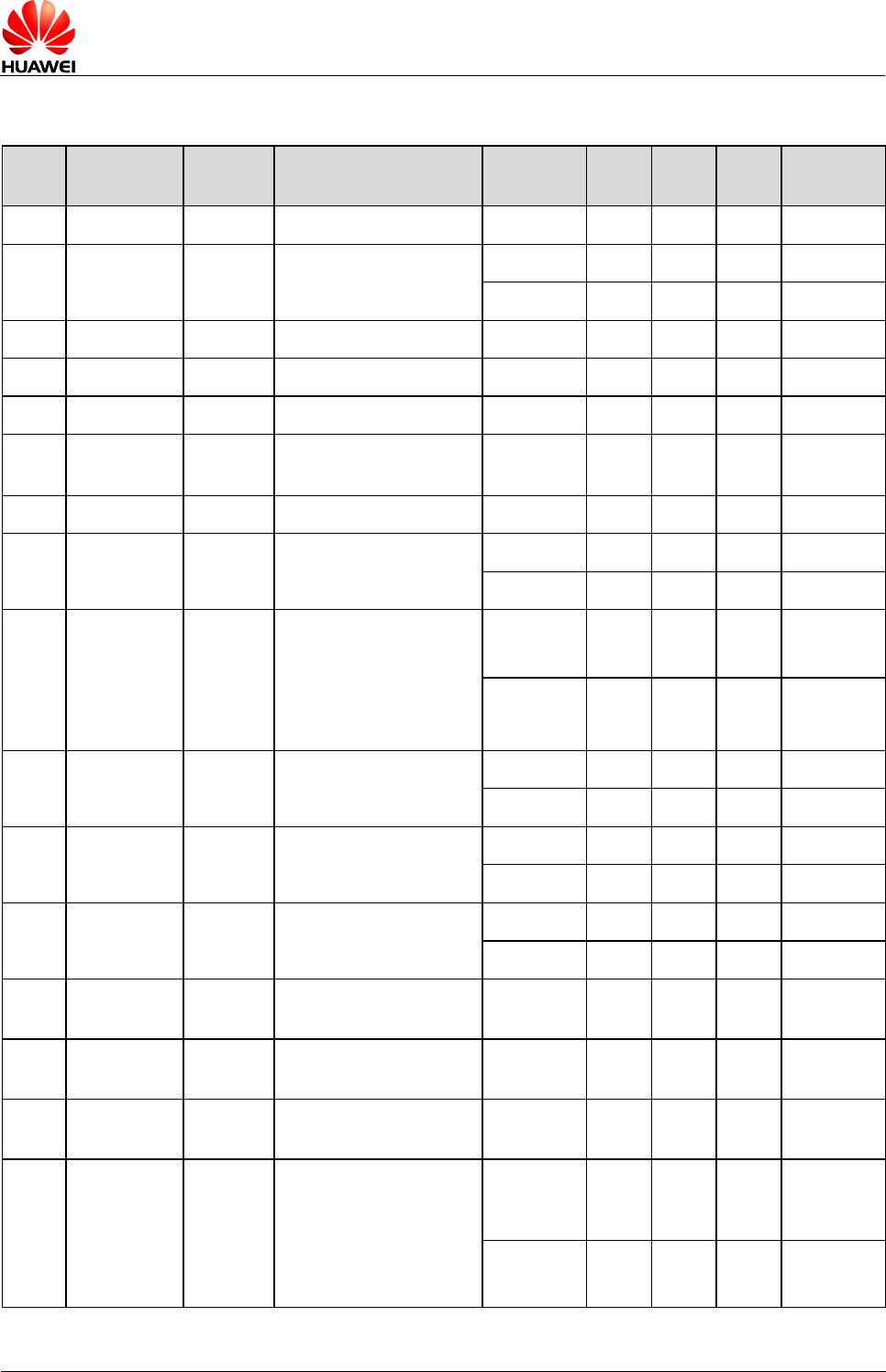
HUAWEI MU739 HSPA+ LGA Module
Hardware Guide
Description of the Application Interfaces
Issue 11 (2015-10-08)
Huawei Proprietary and Confidential
Copyright © Huawei Technologies Co., Ltd.
16
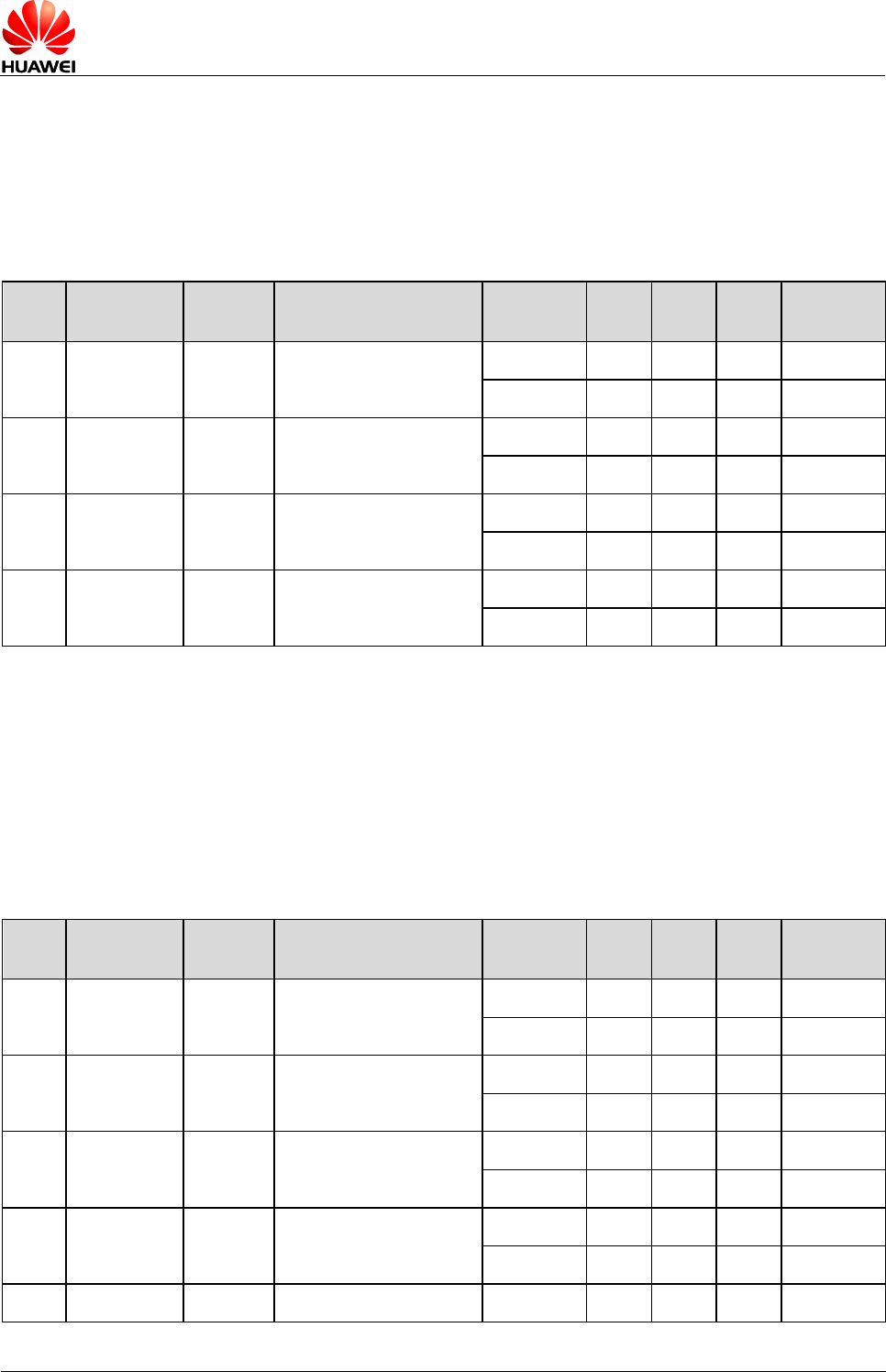
Table 3-1 Definitions of pins on the LGA interface
Pin
No.
Pin Name
Pad Type
Description
Parameter
Min.
(V)
Typ.
(V)
Max.
(V)
Comments
1
NC
-
Not connected
-
-
-
-
-
2
JTAG_TDO
O
JTAG Serial Data Out
VOH
1.35
1.8
2.1
-
VOL
0
-
0.45
3
NC
-
Not connected
-
-
-
-
-
4
NC
-
Not connected
-
-
-
-
-
5
NC
-
Not connected
-
-
-
-
-
6
Reserved
-
Reserved, please keep
this pin open.
-
-
-
-
-
7
NC
-
Not connected
-
-
-
-
-
8
JTAG_TRST
_N
I
JTAG Reset/Module
enable
VIH
1.26
1.8
2.1
-
VIL
–0.3
-
0.63
9
RESOUT_N
O
Output to indicate the
module's hardware is
ready or not.
H: Hardware is ready
L: Hardware is not ready
VOH
1.35
1.8
2.1
-
VOL
0
-
0.45
-
10
JTAG_TMS
I
JTAG State machine
control signal
VIH
1.26
1.8
2.1
-
VIL
–0.3
-
0.63
11
JTAG_TDI
I
JTAG Serial Data Input
VIH
1.26
1.8
2.1
-
VIL
–0.3
-
0.63
12
JTAG_TCK
I
JTAG clock input
VIH
1.26
1.8
2.1
-
VIL
–0.3
-
0.63
13
Reserved
-
Reserved, please keep
this pin open.
-
-
-
-
-
14
Reserved
-
Reserved, please keep
this pin open.
-
-
-
-
-
15
Reserved
-
Reserved, please keep
this pin open.
-
-
-
-
-
16
USIM_DET
I
USIM hot swap detection.
Rising edge for insertion;
falling edge for removal.
H: USIM is present.
L: USIM is absent.
VIH
1.26
1.8
2.1
-
VIL
–0.3
-
0.63
-
HUAWEI MU739 HSPA+ LGA Module
Hardware Guide
Description of the Application Interfaces
Issue 11 (2015-10-08)
Huawei Proprietary and Confidential
Copyright © Huawei Technologies Co., Ltd.
17
Pin
No.
Pin Name
Pad Type
Description
Parameter
Min.
(V)
Typ.
(V)
Max.
(V)
Comments
17
SLEEP_STA
TUS
O
Indicates the sleep status
of MU739
H: MU739 is awake.
L: MU739 is in sleep.
VOH
1.35
1.8
2.1
-
VOL
0
-
0.45
-
18
Reserved
-
Reserved, please keep
this pin open.
-
-
-
-
-
19
Reserved
-
Reserved, please keep
this pin open.
-
-
-
-
20
USIM_VCC
PO
Power supply for USIM
card
-
1.75
1.8
1.98
USIM_PW
R=1.8 V
-
2.75
2.85
3.3
USIM_PW
R=2.85 V
21
Reserved
-
Reserved, please keep
this pin open.
-
-
-
-
-
22
Reserved
-
Reserved, please keep
this pin open.
-
-
-
-
-
23
USB_DP
I/O
High-speed USB D+
-
-
-
-
-
24
USB_DM
I/O
High-speed USB D-
-
-
-
-
-
25
USIM_RST
O
USIM Reset
VOH
0.7 x
USIM
_PW
R
-
3.3
USIM_PW
R=1.8 V or
2.85 V
VOL
0
-
0.2 x
USIM
_PW
R
26
Reserved
-
Reserved, please keep
this pin open.
-
-
-
-
-
27
USIM_CLK
O
USIM Clock
VOH
0.7 x
USIM
_PW
R
-
3.3
USIM_PW
R=1.8 V or
2.85 V
VOL
0
-
0.2 x
USIM
_PW
R
28
Reserved
-
Reserved, please keep
this pin open.
-
-
-
-
-
HUAWEI MU739 HSPA+ LGA Module
Hardware Guide
Description of the Application Interfaces
Issue 11 (2015-10-08)
Huawei Proprietary and Confidential
Copyright © Huawei Technologies Co., Ltd.
18
Pin
No.
Pin Name
Pad Type
Description
Parameter
Min.
(V)
Typ.
(V)
Max.
(V)
Comments
29
USIM_DATA
I/O
USIM Data Input/Output
VOH
0.7 x
USIM
_PW
R
-
3.3
USIM_PW
R=1.8 V or
2.85 V
VOL
0
-
0.2 x
USIM
_PW
R
VIH
0.7 x
USIM
_PW
R
-
3.3
VIL
0
-
0.2 x
USIM
_PW
R
30
Reserved
-
Reserved, please keep
this pin open.
-
-
-
-
-
31
RESET_PM
U_N
I
PMU reset, low active
VIH
1.26
1.8
2.1
-
VIL
–0.3
-
0.63
-
32
USB_VBUS
PI
Power supply for USB
-
3.3
-
5.0
-
33
Reserved
-
Reserved, please keep
this pin open.
-
-
-
-
-
34
BODYSAR_
N
I
Hardware pin for
BODYSAR_N Detection,
active low.
H: No TX power backoff
(default).
L: TX power backoff.
VIH
1.26
1.8
2.1
-
VIL
–0.3
-
0.63
-
35
Reserved
-
Reserved, please keep
this pin open.
-
-
-
-
-
36
Reserved
-
Reserved, please keep
this pin open.
-
-
-
-
-
37
Reserved
-
Reserved, please keep
this pin open.
-
-
-
-
-
38
VCC_EXT1
PO
1.8 V power output
-
1.7
1.8
1.9
-
39
W_DISABLE
_N
I
Flight mode
H: The RF will be turned
VIH
1.26
1.8
2.1
-
HUAWEI MU739 HSPA+ LGA Module
Hardware Guide
Description of the Application Interfaces
Issue 11 (2015-10-08)
Huawei Proprietary and Confidential
Copyright © Huawei Technologies Co., Ltd.
19
Pin
No.
Pin Name
Pad Type
Description
Parameter
Min.
(V)
Typ.
(V)
Max.
(V)
Comments
on (default).
L: The RF will be turned
off.
VIL
–0.3
-
0.63
-
40
VCC_IN
PI
1.8 V power input
-
1.7
1.8
1.9
-
41
Reserved
-
Reserved, please keep
this pin open.
-
-
-
-
-
42
WAKEUP_IN
I
H: MU739 cannot enter
sleep mode.
L: Permit MU739 to enter
sleep mode (default).
VIH
1.26
1.8
2.1
-
VIL
–0.3
-
0.63
-
43
WAKEUP_O
UT
O
Module to wake up the
host
VOH
1.35
1.8
2.1
-
VOL
0
-
0.45
-
44
Reserved
-
Reserved, please keep
this pin open.
-
-
-
-
-
45
Reserved
-
Reserved, please keep
this pin open.
-
-
-
-
-
46
LED#
O
Network status indication
VOH
1.35
1.8
2.1
-
VOL
0
-
0.45
-
47
Reserved
-
Reserved, please keep
this pin open.
-
-
-
-
-
48
ON2_N
I
Turn on the module, low
active
VIH
1.26
1.8
2.1
-
VIL
–0.3
-
0.63
-
49
VBAT_PMU
PI
Battery supply, power
supply for Baseband and
Transceiver
-
3.3
3.8
4.2
-
50
Reserved
-
Reserved, please keep
this pin open.
-
-
-
-
-
51
VBAT_PA
PI
Battery supply, power
supply for PA
-
3.3
3.8
4.2
-
52
VBAT_PA
PI
Battery supply, power
supply for PA
-
3.3
3.8
4.2
-
53
RESET_BB_
N
I
Baseband reset, low
active
VIH
1.26
1.8
2.1
-
VIL
–0.3
-
0.63
-
54
Reserved
-
Reserved, please keep
this pin open.
-
-
-
-
-
55
I2S_CLK0
O
Serial clock
VOH
1.35
1.8
2.1
-
HUAWEI MU739 HSPA+ LGA Module
Hardware Guide
Description of the Application Interfaces
Issue 11 (2015-10-08)
Huawei Proprietary and Confidential
Copyright © Huawei Technologies Co., Ltd.
20
Pin
No.
Pin Name
Pad Type
Description
Parameter
Min.
(V)
Typ.
(V)
Max.
(V)
Comments
VOL
0
-
0.45
-
56
I2S_RX
I
Serial receive data
VIH
1.26
1.8
2.1
-
VIL
–0.3
-
0.63
-
57
I2S_TX
O
Serial transmit data
VOH
1.35
1.8
2.1
-
VOL
0
-
0.45
-
58
I2S_WA0
O
Word alignment select
VOH
1.35
1.8
2.1
-
VOL
0
-
0.45
-
59
Reserved
-
Reserved, please keep
this pin open.
-
-
-
-
-
60
NC
-
Not connected
-
-
-
-
-
61
NC
-
Not connected
-
-
-
-
-
62
GND
-
Ground
-
-
0
-
-
63
GND
-
Ground
-
-
0
-
-
64
GND
-
Ground
-
-
0
-
-
65
MAIN_ANT
-
Main antenna
-
-
-
-
-
66
GND
-
Ground
-
-
0
-
-
67
GND
-
Ground
-
-
0
-
-
68
GND
-
Ground
-
-
0
-
-
69
NC
-
Not connected
-
-
-
-
-
70
GND
-
Ground
-
-
0
-
-
71
GND
-
Ground
-
-
0
-
-
72
AUX_ANT
-
Diversity antenna
-
-
-
-
-
73
GND
-
Ground
-
-
0
-
-
74
GND
-
Ground
-
-
0
-
-
75
NC
-
Not connected
-
-
-
-
-
76
NC
-
Not connected
-
-
-
-
-
77
NC
-
Not connected
-
-
-
-
-
78
NC
-
Not connected
-
-
-
-
-
79
GND
-
Ground
-
-
0
-
-
80
GND
-
Ground
-
-
0
-
-
81
GND
-
Ground
-
-
0
-
-
HUAWEI MU739 HSPA+ LGA Module
Hardware Guide
Description of the Application Interfaces
Issue 11 (2015-10-08)
Huawei Proprietary and Confidential
Copyright © Huawei Technologies Co., Ltd.
21
Pin
No.
Pin Name
Pad Type
Description
Parameter
Min.
(V)
Typ.
(V)
Max.
(V)
Comments
82
GND
-
Ground
-
-
0
-
-
83
GND
-
Ground
-
-
0
-
-
84
GND
-
Ground
-
-
0
-
-
85
GND
-
Ground
-
-
0
-
-
86
GND
-
Ground
-
-
0
-
-
87
GND
-
Ground
-
-
0
-
-
88
GND
-
Ground
-
-
0
-
-
89
GND
-
Ground
-
-
0
-
-
90
GND
-
Ground
-
-
0
-
-
91
GND
-
Ground
-
-
0
-
-
92
GND
-
Ground
-
-
0
-
-
93
GND
-
Ground
-
-
0
-
-
94
GND
-
Ground
-
-
0
-
-
95
GND
-
Ground
-
-
0
-
-
96
GND
-
Ground
-
-
0
-
-
97
GND
-
Ground
-
-
0
-
-
98
GND
-
Ground
-
-
0
-
-
99
GND
-
Ground
-
-
0
-
-
100
GND
-
Ground
-
-
0
-
-
101
GND
-
Ground
-
-
0
-
-
102
GND
-
Ground
-
-
0
-
-
103
GND
-
Ground
-
-
0
-
-
104
GND
-
Ground
-
-
0
-
-
105
GND
-
Ground
-
-
0
-
-
106
GND
-
Ground
-
-
0
-
-
107
GND
-
Ground
-
-
0
-
-
108
GND
-
Ground
-
-
0
-
-
109
GND
-
Ground
-
-
0
-
-
110
GND
-
Ground
-
-
0
-
-
111
GND
-
Ground
-
-
0
-
-
HUAWEI MU739 HSPA+ LGA Module
Hardware Guide
Description of the Application Interfaces
Issue 11 (2015-10-08)
Huawei Proprietary and Confidential
Copyright © Huawei Technologies Co., Ltd.
22
Pin
No.
Pin Name
Pad Type
Description
Parameter
Min.
(V)
Typ.
(V)
Max.
(V)
Comments
112
GND
-
Ground
-
-
0
-
-
113
GND
-
Ground
-
-
0
-
-
114
GND
-
Ground
-
-
0
-
-
- I indicates pins for digital signal input; O indicates pins for digital signal output; PI indicates
power input pins; PO indicates power output pins.
- VIL indicates Low-level Input voltage; VIH indicates High-level Input voltage; VOL indicates
Low-level Output voltage; VOH indicates High-level Output voltage.
- The NC (Not Connected) pins are floating and there are no signal connected to these pins.
- The Reserved pins are internally connected to the module. Therefore, these pins should not
be used, otherwise they may cause problems. Please contact with us for more details about
this information.
3.3 Power Interface
3.3.1 Overview
The power supply part of the MU739 module contains:
- VBAT pin for the power supply
- USIM_VCC pin for USIM card power output
- USB_VBUS pin for USB power supply
- VCC_EXT1 pin for 1.8 V power output
- VCC_IN pin for pin 41–46 voltage supply
Table 3-2 lists the definitions of the pins on the power supply interface.
Table 3-2 Definitions of the pins on the power supply interface
Pin No.
Pin Name
Pad Type
Description
Parameter
Min.
(V)
Typ.
(V)
Max.
(V)
Comments
49
VBAT_PMU
PI
Battery supply, power
supply for Baseband
and Transceiver
-
3.3
3.8
4.2
-
51, 52
VBAT_PA
PI
Battery supply, power
supply for PA
-
3.3
3.8
4.2
-
20
USIM_VCC
PO
Power supply for
USIM card
-
1.75
1.8
1.98
USIM_PW
R=1.8 V
-
2.75
2.85
3.3
USIM_PW
R=2.85 V
HUAWEI MU739 HSPA+ LGA Module
Hardware Guide
Description of the Application Interfaces
Issue 11 (2015-10-08)
Huawei Proprietary and Confidential
Copyright © Huawei Technologies Co., Ltd.
23
Pin No.
Pin Name
Pad Type
Description
Parameter
Min.
(V)
Typ.
(V)
Max.
(V)
Comments
32
USB_VBUS
PI
Power supply for USB
It is connected to
VBAT_PMU (default).
-
3.3
-
5.0
-
38
VCC_EXT1
PO
1.8 V power output
-
1.7
1.8
1.9
-
40
VCC_IN
PI
1.8 V power input
-
1.7
1.8
1.9
-
62–64,
66–68,
70, 71,
73, 74,
79–114
GND
-
Ground
-
-
0
-
-
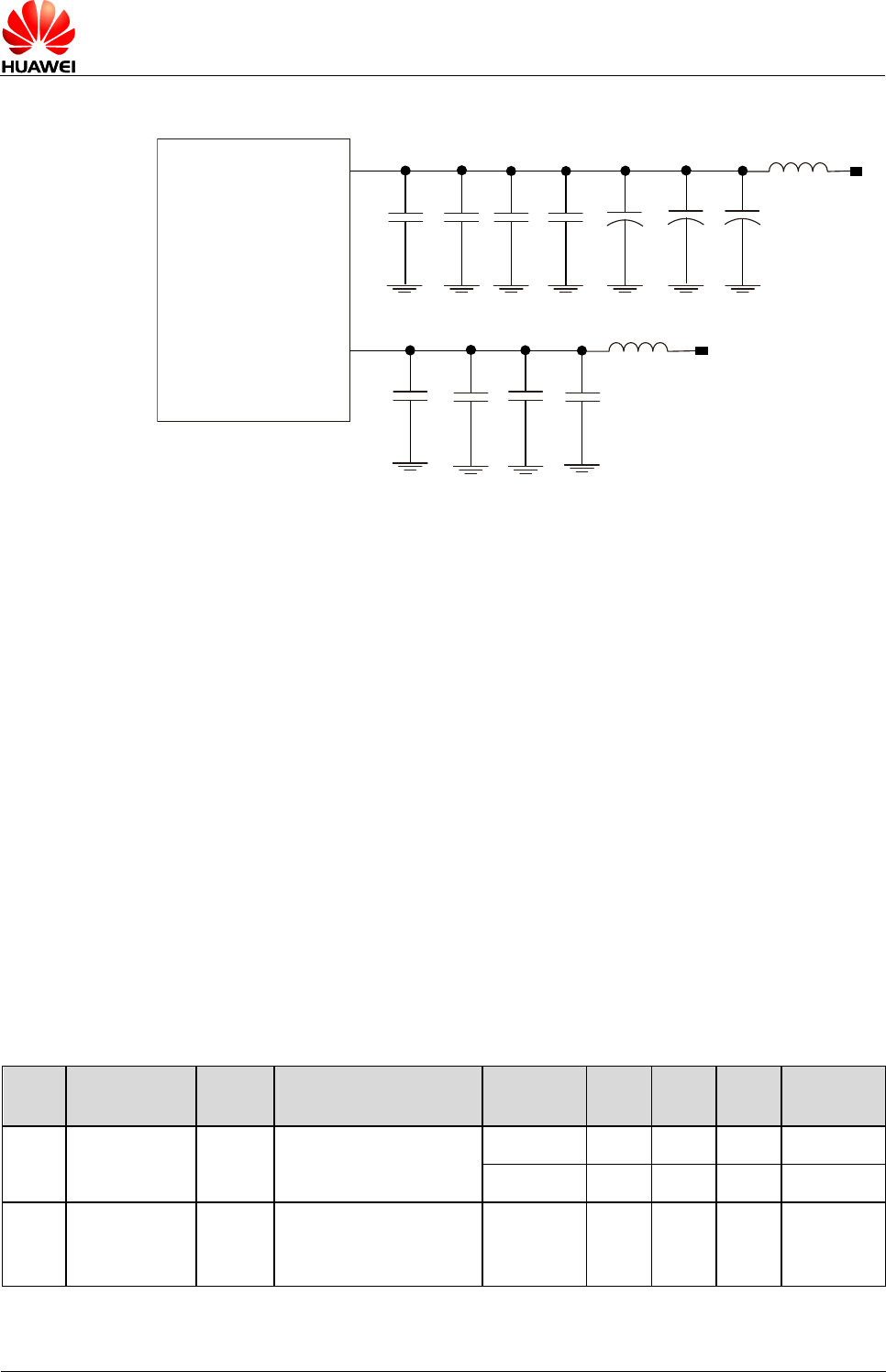
3.3.2 VBAT Interface
When the MU739 module works normally, power is supplied through the VBAT_PMU
and VBAT_PA pins and the voltage ranges from 3.3 V to 4.2 V (typical value is 3.8 V).
The 114-pin LGA module provides one VBAT_PMU pin, two VBAT_PA pins and
forty-six GND pins. To ensure that the MU739 module works normally, all the pins
must be connected.
When the MU739 module is used for different applications, special attention should be
paid to the design of the power supply. When the MU739 module transmits at the
maximum power, the transient peak current may reach 2.75 A. In this case, the
VBAT_PA voltage drops. Make sure that the voltage does not decrease below 3.3 V in
any case. Otherwise, exceptions such as reset of the MU739 module may occur.
A low-dropout (LDO) regulator or switch-mode power supply with load current larger
than 3 A is recommended. At least three 220 µF capacitors should be installed to
VBAT_PA pins. And the trace of the power supply should be as short and wide as
possible.
It is recommended to employ a ferrite bead in series on VBAT to improve the EMI
performance. FBMJ1608HS280NT manufactured by TAIYO YUDEN or
MPZ1608S300ATAH0 manufactured by TDK is recommended.
Figure 3-2 shows the recommended power circuit of MU739 module.
HUAWEI MU739 HSPA+ LGA Module
Hardware Guide
Description of the Application Interfaces
Issue 11 (2015-10-08)
Huawei Proprietary and Confidential
Copyright © Huawei Technologies Co., Ltd.
24
Figure 3-2 Recommended power circuit of MU739 module
Module
(Modem)
VBAT_PA VBAT
22 μF
++
+
220 μF
220 μF220 μF
1μF
100 nF
330 pF
VBAT_PMU VBAT
22 μF
1μF
100 nF330 pF
Ferrite bead
Ferrite bead
3.4 Signal Control Interface
3.4.1 Overview
The signal control part of the interface in the MU739 module consists of the following:
- Power on pins (ON2_N)
- RESOUT_N pin
- PMU reset pin (RESET_PMU_N)
- Baseband reset pin (RESET_BB_N)
- Network status LED pin (LED#)
- W_DISABLE_N signal pin
- WAKEUP_IN signal pin
- WAKEUP_OUT signal pin
- SLEEP_STATUS signal pin
Table 3-3 lists the pins on the signal control interface.
Table 3-3 Pins on the signal control interface
Pin
No.
Pin Name
Pad
Type
Description
Parameter
Min.
(V)
Typ.
(V)
Max.
(V)
Comments
48
ON2_N
I
Turn on the module, low
active
VIH
1.26
1.8
2.1
-
VIL
–0.3
-
0.63
-
9
RESOUT_N
O
Output to indicate the
module's hardware is
ready or not.
VOH
1.35
1.8
2.1
-
HUAWEI MU739 HSPA+ LGA Module
Hardware Guide
Description of the Application Interfaces
Issue 11 (2015-10-08)
Huawei Proprietary and Confidential
Copyright © Huawei Technologies Co., Ltd.
25
Pin
No.
Pin Name
Pad
Type
Description
Parameter
Min.
(V)
Typ.
(V)
Max.
(V)
Comments
H: Hardware is ready
L: Hardware is not ready
VOL
0
-
0.45
-
31
RESET_PMU_
N
I
PMU reset, low active
VIH
1.26
1.8
2.1
-
VIL
–0.3
-
0.63
-
53
RESET_BB_N
I
Baseband reset, low
active
VIH
1.26
1.8
2.1
-
VIL
–0.3
-
0.63
-
39
W_DISABLE_
N
I
Flight mode
H: The RF will be turned
on (default).
L: The RF will be turned
off.
VIH
1.26
1.8
2.1
-
VIL
–0.3
-
0.63
-
46
LED#
O
Network status indication
VOH
1.35
1.8
2.1
-
VOL
0
-
0.45
-
42
WAKEUP_IN
I
H: MU739 can’t enter
sleep mode.
L: Permit MU739 to enter
sleep mode (default).
VIH
1.26
1.8
2.1
-
VIL
–0.3
-
0.63
-
43
WAKEUP_OU
T
O
Module to wake up the
host
VOH
1.35
1.8
2.1
-
VOL
0
-
0.45
-
17
SLEEP_STAT
US
O
Indicates the sleep status
of MU739
H: MU739 is awake.
L: MU739 is in sleep.
VOH
1.35
1.8
2.1
-
VOL
0
-
0.45
-
16
USIM_DET
I
USIM hot swap detection.
Rising edge for insertion;
falling edge for removal.
H: USIM is present.
L: USIM is absent.
VIH
1.26
1.8
2.1
-
VIL
–0.3
-
0.63
-
34
BODYSAR_N
I
Hardware pin for
BODYSAR_N Detection,
active low.
H: No TX power backoff
(default).
L: TX power backoff.
VIH
1.26
1.8
2.1
-
VIL
–0.3
-
0.63
-
It is recommended to use a resistor of 0 Ω in the AP side to isolate signals transmitted from
above pins in Table 3-3 .
HUAWEI MU739 HSPA+ LGA Module
Hardware Guide
Description of the Application Interfaces
Issue 11 (2015-10-08)
Huawei Proprietary and Confidential
Copyright © Huawei Technologies Co., Ltd.
26
3.4.2 Input Signal Control Pins
The MU739 module implements power-on and resets the hardware through the input
signal control pins. The power-on and reset control parts of the interface of the MU739
module include ON2_N interface signal and the baseband reset interface signal
RESET_BB_N and the PMU reset signal RESET_PMU_N.
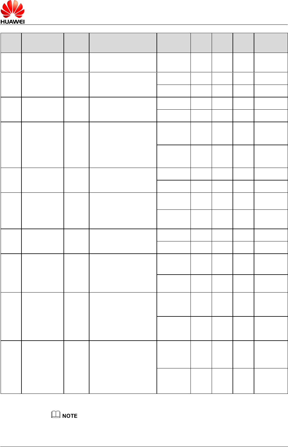
TURN ON
The ON2_N pin is used to implement turning on the module.
The ON2_N pin is low level active.
ON2_N can be controlled by a host processor GPIO (with internal pull-up under reset),
when tied to GND, this input can be used to force an automatic booting up when
power is applied or after a hard reset is performed.
Figure 3-3 Connections of ON2_N pin
ON2_N
Module
(Modem)
Micro Control
(AP)
ON_N
2.2 kΩ
b
c
e
Power On Time
It is recommended to power on module use the ON2_N pin.
After VBAT_PMU has been applied and been stable, the module will wait for an
on-event and if the on signal is available, the module will be powered on.
During power on timing, please make sure the VBAT_PMU is stable.
ON2_N can power on the module.
Figure 3-4 Power on timing sequence
HUAWEI MU739 HSPA+ LGA Module
Hardware Guide
Description of the Application Interfaces
Issue 11 (2015-10-08)
Huawei Proprietary and Confidential
Copyright © Huawei Technologies Co., Ltd.
27
Table 3-4 Power on timing
Parameter
Comments
Time (Min value)
Unit
TON2_N
ON2_N turn on time
40
µs
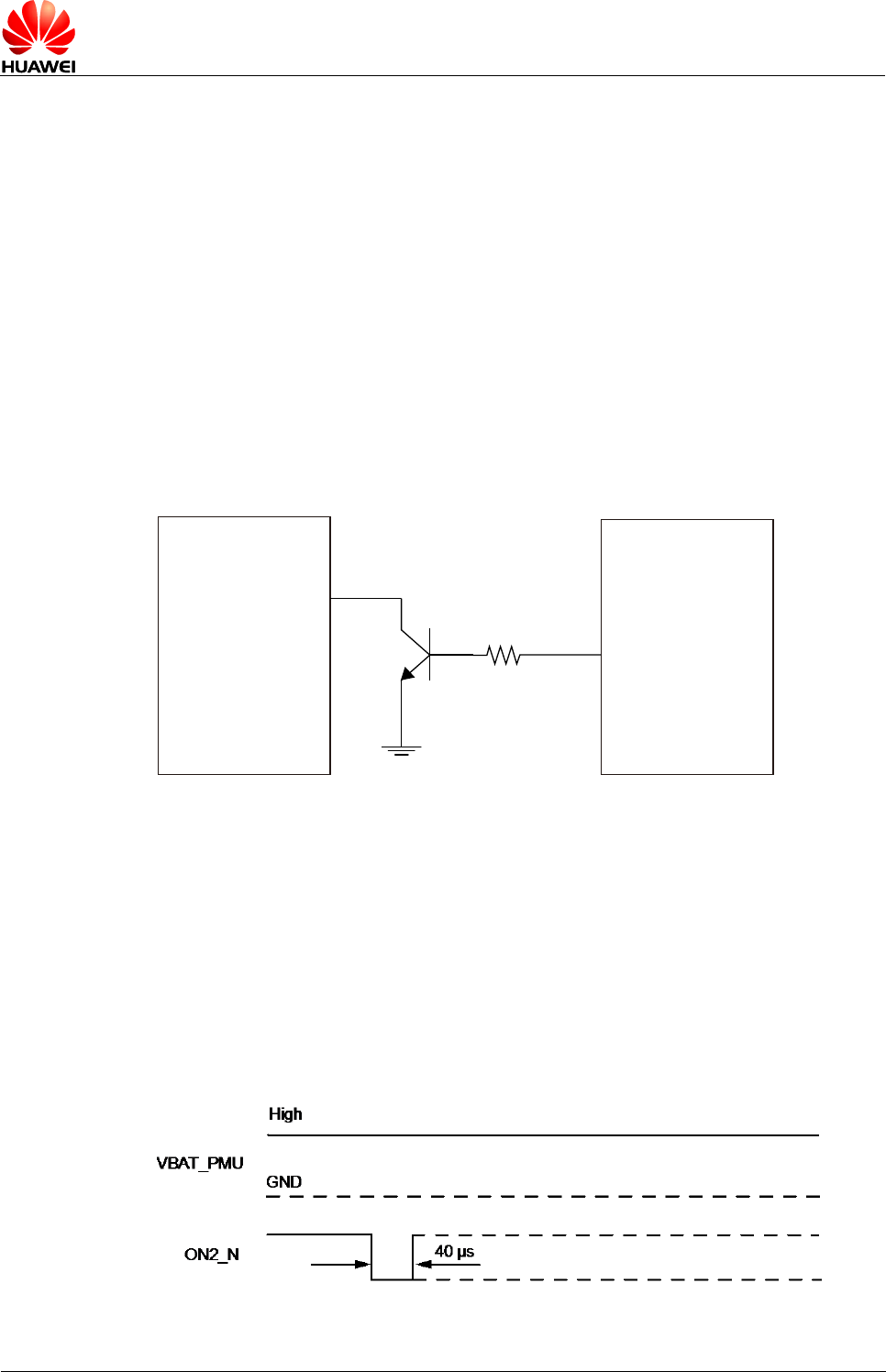
Power Off Time
Figure 3-5 Power supply time sequence for power cycling
Parameter
Remarks
Time(Min.)
Unit
Toff
Power off time
100
ms
MU739 does not support hardware shutting down, and it can only be powered off by cutting off
the power supply.
RESET
The RESET_PMU_N pin is used to make a hard reset.
- Active low with internal pull-up (200 kΩ)
- Initiate power down of the modem system (baseband, PMU, RF&clocks)
The RESET_BB_N pin is used to make a software reset.
HUAWEI MU739 HSPA+ LGA Module
Hardware Guide
Description of the Application Interfaces
Issue 11 (2015-10-08)
Huawei Proprietary and Confidential
Copyright © Huawei Technologies Co., Ltd.
28
- Active low without pull-up or pull-down
- Resets baseband sub-system.
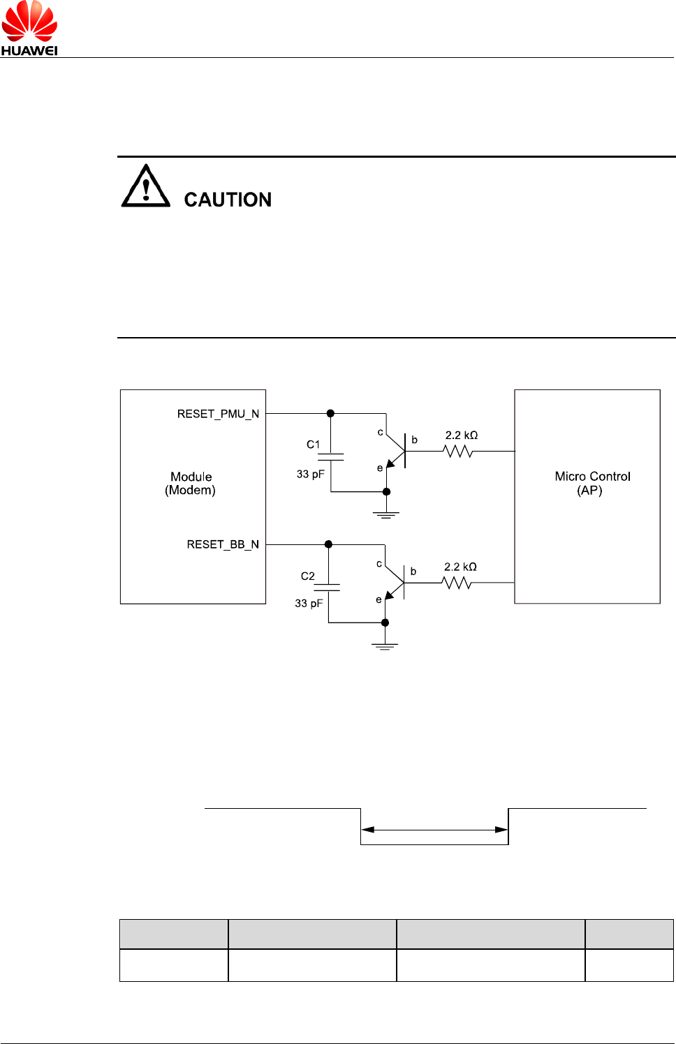
As the RESET_PMU_N and RESET_BB_N signals are relatively sensitive; it is
recommended that you install a 33 pF capacitor near these pins of the interfaces for
filtering. In addition, when you design a circuit on the PCB of the interface board, it is
recommended that the circuit length not exceed 20 mm and that the circuit be kept at
a distance of 2.54 mm (100 mil) at least from the PCB edge. Furthermore, it is
recommended to wrap the area adjacent to the signal wire with a ground wire.
Otherwise, the module may be reset due to interference.
Figure 3-6 Connections of RESET_BB_N and RESET_PMU_N pins
It is recommended to reset module using the RESET_BB_N.
When a low-level pulse is supplied through the RESET_PMU_N or RESET_BB_N for
about 20 ms, the module will be reset.
Figure 3-7 Reset timing
Tpd=20 ms
RESET_BB_N
RESET_PMU_N
Table 3-5 Reset timing
Parameter
Comments
Time (Typical value)
Unit
Tpd
Reset time
20
ms
HUAWEI MU739 HSPA+ LGA Module
Hardware Guide
Description of the Application Interfaces
Issue 11 (2015-10-08)
Huawei Proprietary and Confidential
Copyright © Huawei Technologies Co., Ltd.
29
W_DISABLE_N
When W_DISABLE_N is low, the RF will be turned OFF;
When W_DISABLE_N is high, the RF will be turned ON.
Figure 3-8 W_DISABLE_N timing
RF ON
RF ON
RF OFF
RF OFF
W_DISABLE_N
W_DISABLE_N
WAKEUP_IN
This is the authorization signal of MU739 entering sleep mode.
If this signal is pulled up to high (1.8 V) level, MU739 cannot enter sleep mode.
If this signal is low or open, MU739 is allowed to enter sleep mode normally.
Figure 3-9 WAKEUP_IN timing
MU739 can not enter
sleep mode.
MU739 is allowed to enter
sleep mode normally.
WAKEUP_IN
USIM_DET
MU739 supports USIM Hot Swap function.
MU739 provides an input pin (USIM_DET) to detect whether the USIM card is present
or not. This pin is an edge trigger pin.
Table 3-6 Function of the USIM_DET pin
No.
USIM_DET
Function
1
Rising edge
USIM Card insertion.
If the USIM Card is present, USIM_DET should be high.
2
Falling edge
USIM Card removal.
If the USIM Card is absent, USIM_DET should be low.
HUAWEI MU739 HSPA+ LGA Module
Hardware Guide
Description of the Application Interfaces
Issue 11 (2015-10-08)
Huawei Proprietary and Confidential
Copyright © Huawei Technologies Co., Ltd.
30
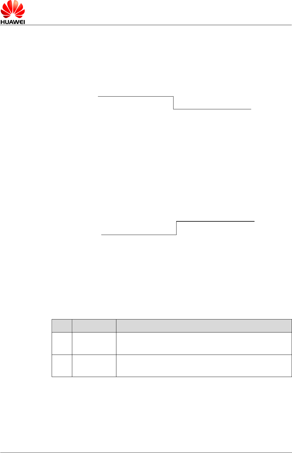
Figure 3-10 Connections of the USIM_DET pin
Module
VCC_EXT1
USIM_DET
100k
470pF
USIM Socket
CD
CD is a pin detecting USIM in the USIM socket, in normal, there will be a detect pin in
the USIM Socket.
The Normal SHORT USIM connector should be employed. The logic of USIM_DET is
shown as below. High represents that USIM is inserted; Low represents that USIM is
removed.
USIM Connector Switch
USIM installed=
Not Connected
USIM not
installed=
GND
USIM_DET
When USIM is inserted (hot), USIM_DET will change from Low to High;
When USIM is removed (hot), USIM_DET will change from High to Low;
MU739 will detect the rising or falling edge of USIM_DET to react the hot swap.
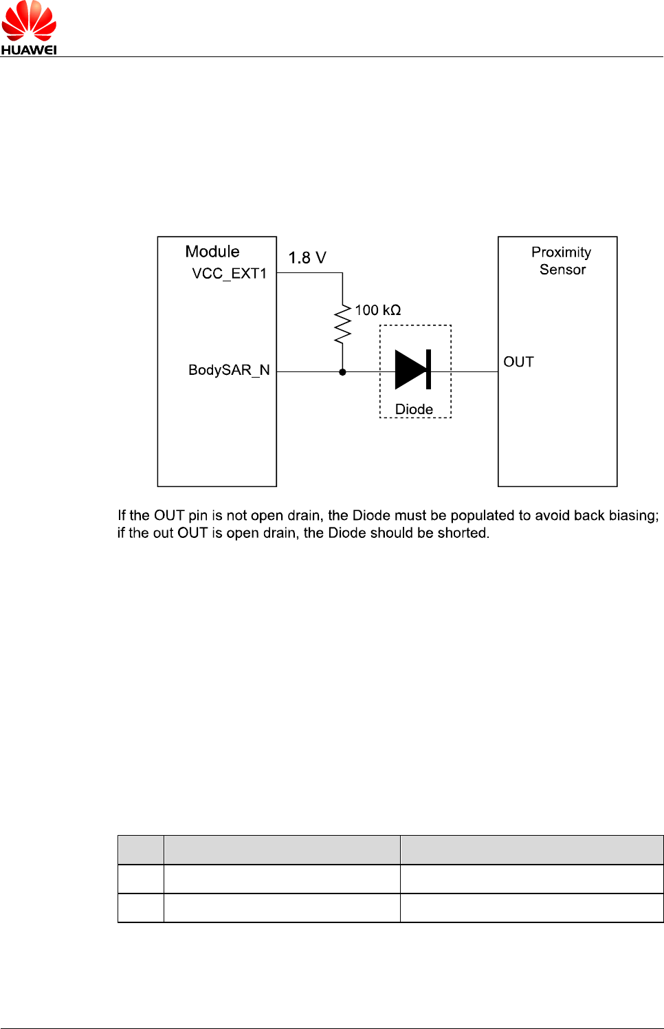
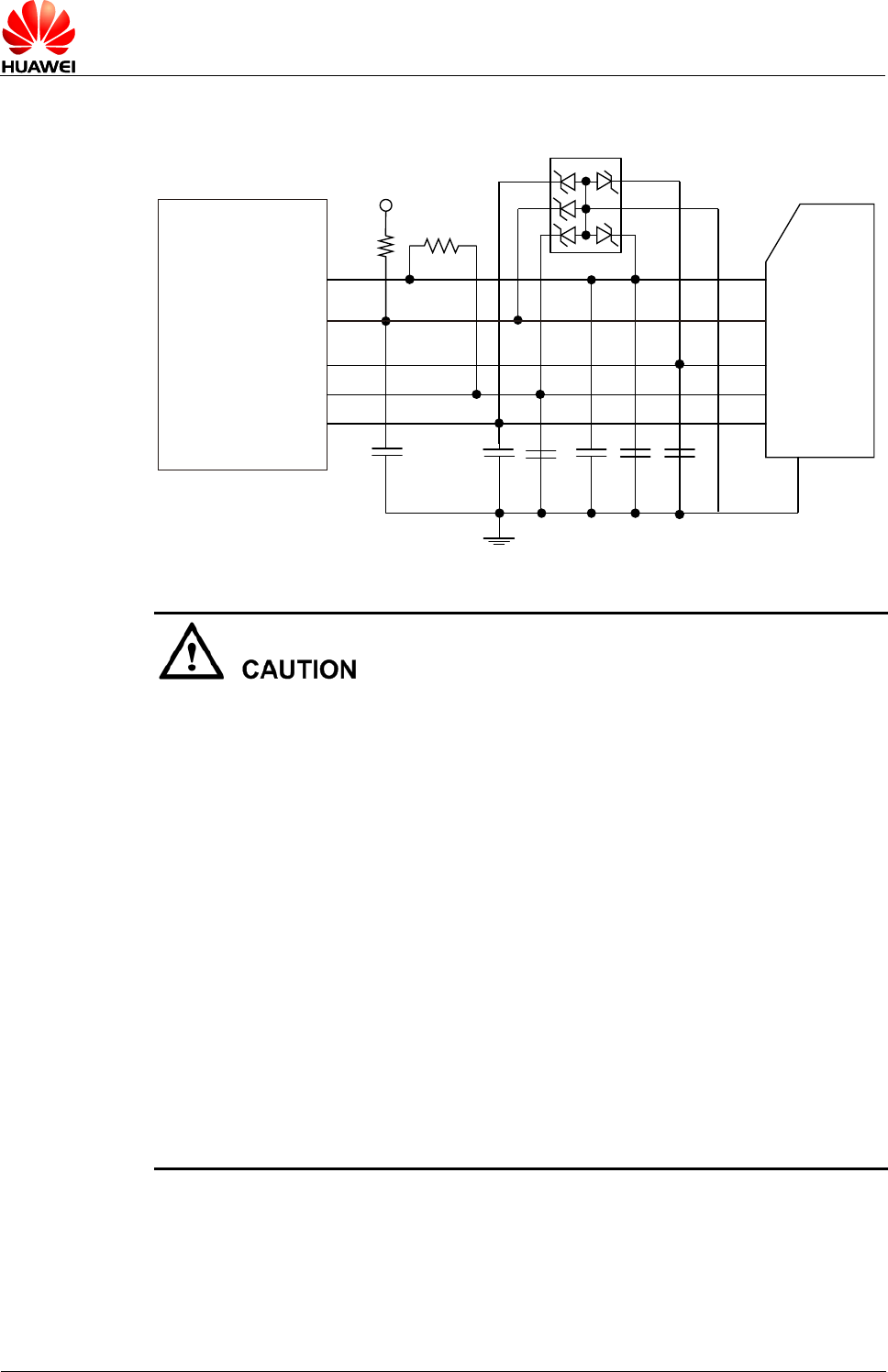
BODYSAR_N
The BODYSAR_N signal is used to monitor the proximity sensor's output and trigger
the power backoff actions. It is low active.
There are some essential preconditions:
HUAWEI MU739 HSPA+ LGA Module
Hardware Guide
Description of the Application Interfaces
Issue 11 (2015-10-08)
Huawei Proprietary and Confidential
Copyright © Huawei Technologies Co., Ltd.
31
- MU739 cannot provide any control signal for the proximity sensor; any control or
programming required by the P sensor should be handled by the PC side.
- MU739 can only provide one pin (pin 34) as the input, and this pin is the one and
only connection between the proximity sensors.
- As for the one pin connection, voltage level translation and back biasing
protection issues should be handled by the PC side.
Figure 3-11 Connections of the BodySAR_N pin
The diode should be a Schottky diode with extremely low forward voltage.
The key parameters of the diode are as below:
IR<1 μA (at 125°C ), VF<0.4 V (when If=1 mA)
SBR0230T5 (Diodes) or RB520S30T1G (ON) is recommended.
3.4.3 Output Signal Control Pins
The MU739 module provides an LED control pin (LED#).
The pulse signal output through this pin controls the status of the LED on the user
interface board to display the RF status.
Table 3-7 List of the LED# pin
No.
Operating Status
LED_STATUS
1
RF function is turned on
Output high
2
RF function is turned off
Output low
Figure 3-12 shows the recommended circuits of the LED# pin. According to LED
feature, you can adjust the LED brightness by adjusting the impedance of resistor.
HUAWEI MU739 HSPA+ LGA Module
Hardware Guide
Description of the Application Interfaces
Issue 11 (2015-10-08)
Huawei Proprietary and Confidential
Copyright © Huawei Technologies Co., Ltd.
32
Figure 3-12 Driving circuit
Module
(Modem)
LED#
LED
VBAT
c
e
100 nF
b
22 kΩ
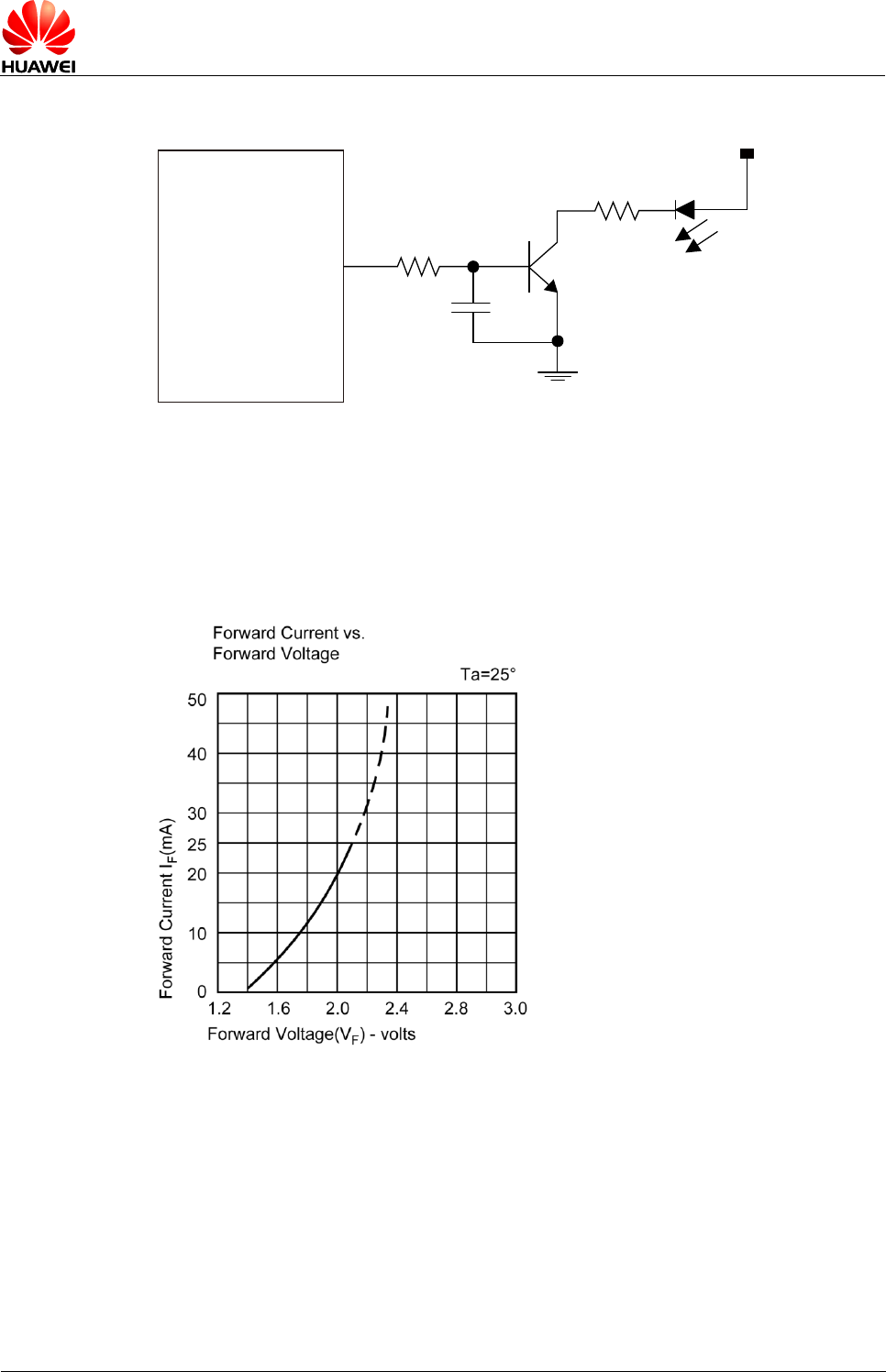
It is recommended to use the triode of DTC144EET1G, LDTC144EET1G or
PDTC144EE.115 in Figure 3-12 .
The brightness of the LED depends on the current value, and for most of the indicator
lights the current from 2 mA to 5 mA is already enough.
Figure 3-13 LED Typical Electro-Optical Characteristics Curves
SLEEP_STATUS
The SLEEP_STATUS signal is used to indicate the status of MU739. The AP can get
to know whether the module is in sleep or not by reading this pin.
When SLEEP_STATUS signal is high, MU739 is in normal work status.
When SLEEP_STATUS signal is low, MU739 is in sleep status.
HUAWEI MU739 HSPA+ LGA Module
Hardware Guide
Description of the Application Interfaces
Issue 11 (2015-10-08)
Huawei Proprietary and Confidential
Copyright © Huawei Technologies Co., Ltd.
33
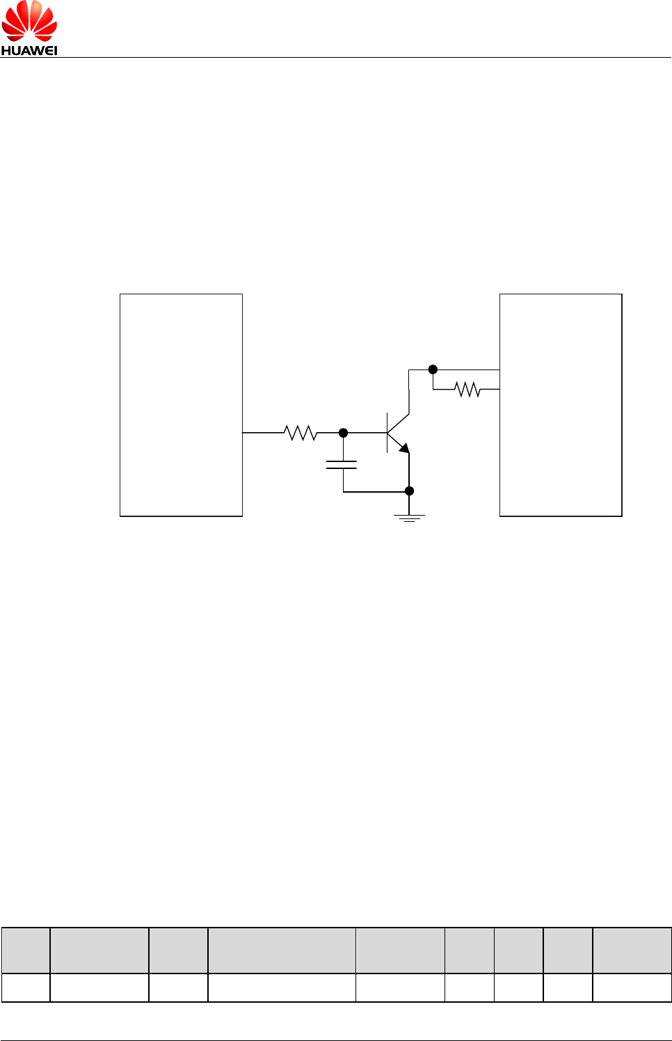
WAKEUP_OUT
The WAKEUP_OUT signal is used to wake up the AP.
WAKEUP_OUT signal is low by default. When a phone call or an SMS is coming, the
MU739 module will output a high pulse which lasts for 1s.
Within the duration of the high pulse, if a new phone call or an SMS is coming, the
MU739 module will output the high pulse over again.
Table 3-3 shows the definition of the WAKEUP_OUT signal.
Figure 3-14 Connections of the WAKEUP_OUT pin
Module
(Modem)
WAKEUP_OUT
c
e
100 nF
b
22 kΩ
VCC_EXT
Micro Control
(AP)
100 kΩ
It is recommended to use the triode of DTC144EET1G, LDTC144EET1G or
PDTC144EE.115 in Figure 3-14 .
RESOUT_N
RESOUT_N is an output of the module and is used to indicate the hardware of
module is ready. Once system powers on, the RESOUT_N signal can be routed to the
AP processor to allow the AP to monitor and detect resets of the modem system.
During reset, RESOUT_N is an output signal, logic low. RESOUT_N would be
monitored by a host processor GPIO (with internal pull-up).
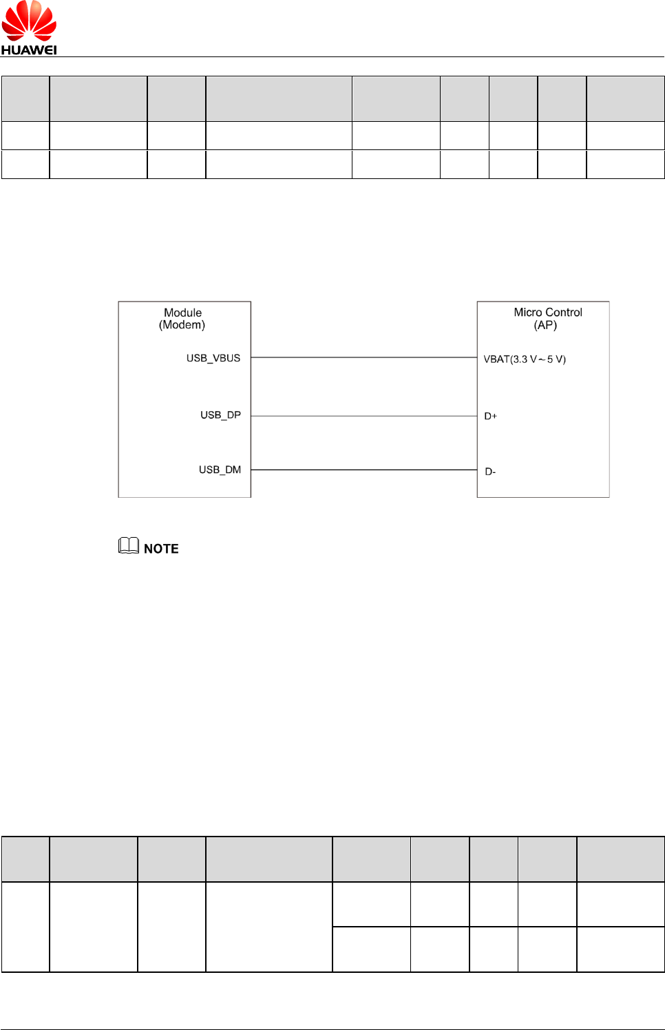
3.5 USB Interface
The MU739 is compliant with USB 2.0 high speed protocol. The USB interface is
powered from the USB_VBUS supply. The USB input/output lines are compatible with
the USB 2.0 VBAT signal specifications. Figure 3-15 shows the circuit of the USB
interface.
Table 3-8 Definition of the USB interface
Pin
No.
Pin Name
Pad
Type
Description
Parameter
Min.
(V)
Typ.
(V)
Max.
(V)
Comments
23
USB_DP
I/O
High-speed USB D+
-
-
-
-
-
HUAWEI MU739 HSPA+ LGA Module
Hardware Guide
Description of the Application Interfaces
Issue 11 (2015-10-08)
Huawei Proprietary and Confidential
Copyright © Huawei Technologies Co., Ltd.
34
Pin
No.
Pin Name
Pad
Type
Description
Parameter
Min.
(V)
Typ.
(V)
Max.
(V)
Comments
24
USB_DM
I/O
High-speed USB D-
-
-
-
-
-
32
USB_VBUS
PI
Power supply for USB
-
3.3
-
5.0
-
According to USB protocol, for bus timing or electrical characteristics of MU739 USB
signal please refer to the chapter 7.3.2 of Universal Serial Bus Specification 2.0.
Figure 3-15 Recommended circuit of USB interface
- The layout design of this circuit on the AP board should comply with the USB 2.0 high speed
protocol, with differential impedance control to 90 Ω.
- It is recommended that set USB_DP and USB_DM pins as test points and then place these
test points on the AP for debug.
3.6 USIM Card Interface
3.6.1 Overview
The MU739 module provides a USIM card interface complying with the ISO 7816-3
standard and supports automatic detection of a 3.0 V USIM card or a 1.8 V USIM card.
Table 3-9 lists the USIM card interface signals.
Table 3-9 USIM card interface signals
Pin
No.
Pin Name
Pad Type
Description
Parameter
Min.
(V)
Typ.
(V)
Max.
(V)
Comments
20
USIM_VCC
PO
Power supply for
USIM card
-
1.75
1.8
1.98
USIM_PWR
=1.8 V
-
2.75
2.85
3.3
USIM_PWR
=2.85 V
HUAWEI MU739 HSPA+ LGA Module
Hardware Guide
Description of the Application Interfaces
Issue 11 (2015-10-08)
Huawei Proprietary and Confidential
Copyright © Huawei Technologies Co., Ltd.
35
Pin
No.
Pin Name
Pad Type
Description
Parameter
Min.
(V)
Typ.
(V)
Max.
(V)
Comments
25
USIM_RST
O
USIM Reset
VOH
0.7 x
USIM_
PWR
-
3.3
USIM_PWR
=1.8 V or
2.85 V
VOL
0
-
0.2 x
USIM_
PWR
27
USIM_CLK
O
USIM Clock
VOH
0.7 x
USIM_
PWR
-
3.3
USIM_PWR
=1.8 V or
2.85 V
VOL
0
-
0.2 x
USIM_
PWR
29
USIM_DATA
I/O
USIM Data
Input/Output
VOH
0.7 x
USIM_
PWR
-
3.3
USIM_PWR
=1.8 V or
2.85 V
VOL
0
-
0.2 x
USIM_
PWR
VIH
0.7 x
USIM_
PWR
-
3.3
VIL
0
-
0.2 x
USIM_
PWR
16
USIM_DET
I
USIM hot swap
detection.
Rising edge for
insertion; falling
edge for removal.
H: USIM is present.
L: USIM is absent.
VIH
1.26
1.8
2.1
VIL
–0.3
-
0.63
3.6.2 Circuit Recommended for the USIM Card Interface
As the MU739 module is not equipped with a USIM card socket, you need to place a
USIM card socket on the user interface board. The USIM card signals are transmitted
outwards through the 114-pin LGA interface. Figure 3-16 shows the circuit of the
USIM card interface.
There is no pull-up resistor on USIM_DATA inside the MU739 module, so an external resistor
(4.7 kΩ recommended) must be added between USIM_DATA and USIM_VCC.
HUAWEI MU739 HSPA+ LGA Module
Hardware Guide
Description of the Application Interfaces
Issue 11 (2015-10-08)
Huawei Proprietary and Confidential
Copyright © Huawei Technologies Co., Ltd.
36
Figure 3-16 Circuit of the USIM card interface
USIM
Module
(Modem)
33 pF 33 pF 33 pF 33 pF
ESD protection
USIM_VCC
USIM_CLK
USIM_DATA
USIM_RST
33 nF 1 µF
4.7 kΩ
USIM_DET
4.7 kΩ
VCC_EXT1_1V8
- The ESD protection component should choose low capacitance. The capacitance
of the component should be less than 10 pF.
- To meet the requirements of 3GPP TS 51.010-1 protocols and electromagnetic
compatibility (EMC) authentication, the USIM socket should be placed near the
LGA interface (it is recommended that the PCB circuit connects the LGA interface
and the USIM socket does not exceed 100 mm), because a long circuit may lead to
wave distortion, thus affecting signal quality.
- It is recommended that you wrap the area adjacent to the USIM_CLK and
USIM_DATA signal wires with ground. The Ground pin of the USIM socket and the
Ground pin of the USIM card must be well connected to the power Ground pin
supplying power to the MU739 module.
- A 1 uF capacitor and a 33 pF capacitor are placed between the USIM_VCC and
Ground pins in parallel. Three 33 pF capacitors are placed between the
USIM_DATA and Ground pins, the USIM_RST and Ground pins, and the
USIM_CLK and Ground pins in parallel to filter interference from RF signals.
- It is recommended to take electrostatic discharge (ESD) protection measures near
the USIM card socket. Transient voltage suppressor diode should be placed as
close as possible to the USIM socket, and the Ground pin of the ESD protection
component is well connected to the power Ground pin that supplies power to the
MU739 module.
HUAWEI MU739 HSPA+ LGA Module
Hardware Guide
Description of the Application Interfaces
Issue 11 (2015-10-08)
Huawei Proprietary and Confidential
Copyright © Huawei Technologies Co., Ltd.
37
3.7 Audio Interface
MU739 provides one I2S interface to support the audio function, and it can be only
used in the master mode. If customers need the audio function in their product, please
contact with us for more details.
Table 3-10 I2S interface signals
Pin
No.
Pin Name
Pad Type
Description
Parameter
Min.
(V)
Typ.
(V)
Max.
(V)
Comments
55
I2S_CLK0
O
Serial clock
VOH
1.35
1.8
2.1
-
VOL
0
-
0.45
-
56
I2S_RX
I
Serial receive data
VIH
1.26
1.8
2.1
-
VIL
–0.3
-
0.63
-
57
I2S_TX
O
Serial transmit data
VOH
1.35
1.8
2.1
-
VOL
0
-
0.45
-
58
I2S_WA0
O
Word alignment select
VOH
1.35
1.8
2.1
-
VOL
0
-
0.45
-
3.8 JTAG Interface
MU739 module provides one JTAG interface (Joint Test Action Group). It is
recommended that set the 5 pins related to JTAG interface as test points on the AP for
tracing and debugging.
Table 3-11 Signals on the JTAG interface
Pin
No.
Pin Name
Pad Type
Description
Parameter
Min.
(V)
Typ.
(V)
Max.
(V)
Comments
2
JTAG_TDO
O
JTAG Serial Data Out
VOH
1.35
1.8
2.1
-
VOL
0
-
0.45
8
JTAG_TRST
_N
I
JTAG Reset/Module
enable
VIH
1.26
1.8
2.1
-
VIL
–0.3
-
0.63
10
JTAG_TMS
I
JTAG State machine
control signal
VIH
1.26
1.8
2.1
-
VIL
–0.3
-
0.63
11
JTAG_TDI
I
JTAG Serial Data Input
VIH
1.26
1.8
2.1
-
VIL
–0.3
-
0.63
12
JTAG_TCK
I
JTAG clock input
VIH
1.26
1.8
2.1
-
HUAWEI MU739 HSPA+ LGA Module
Hardware Guide
Description of the Application Interfaces
Issue 11 (2015-10-08)
Huawei Proprietary and Confidential
Copyright © Huawei Technologies Co., Ltd.
38
Pin
No.
Pin Name
Pad Type
Description
Parameter
Min.
(V)
Typ.
(V)
Max.
(V)
Comments
VIL
–0.3
-
0.63
It is suggested to place the above 5 test points on the AP board for debug.
3.9 RF Antenna Interface
MU739 module provides 2 antenna interfaces for connecting the external antennas.
Table 3-12 Signals on RF Antenna interface
Pin
No.
Pin Name
Pad Type
Description
Parameter
Min.
(V)
Typ.
(V)
Max.
(V)
Comments
65
MAIN_ANT
-
Main antenna
-
-
-
-
-
72
AUX_ANT
-
Diversity antenna
-
-
-
-
-
3.10 Reserved Interface
The module provides some reserved pins. All of reserved pins cannot be used by the
customer. Please keep these pins open.
Table 3-13 Reserved pins
Pin No.
Pin Name
Pad Type
Description
Parameter
Min.
(V)
Typ.
(V)
Max.
(V)
Comments
6, 13-15,18,19, 21,
22, 26, 28, 30, 33,
35-37, 41, 44, 45,
47, 50, 54, 59
Reserved
-
Reserved,
please keep
this pin
open.
-
-
-
-
-
3.11 NC Interface
The MU739 module has some NC pins. There are no signal connected to these pins.
HUAWEI MU739 HSPA+ LGA Module
Hardware Guide
Description of the Application Interfaces
Issue 11 (2015-10-08)
Huawei Proprietary and Confidential
Copyright © Huawei Technologies Co., Ltd.
39
Table 3-14 NC pins
Pin No.
Pin Name
Pad Type
Description
Parameter
Min.
(V)
Typ.
(V)
Max.
(V)
Comments
1, 3-5, 7, 60, 61, 69,
75-78
NC
-
Not
connected
-
-
-
-
-
HUAWEI MU739 HSPA+ LGA Module
Hardware Guide
RF Specifications
Issue 11 (2015-10-08)
Huawei Proprietary and Confidential
Copyright © Huawei Technologies Co., Ltd.
40
4 RF Specifications
4.1 About This Chapter
This chapter describes the RF specifications of the MU739 module, including:
- Operating Frequencies
- Conducted RF Measurement
- Conducted Rx Sensitivity and Tx Power
- Antenna Design Requirements
4.2 Operating Frequencies
Table 4-1 shows the RF bands supported by MU739.
Table 4-1 RF bands
Operating Band
Tx
Rx
WCDMA Band 1
1920 MH–1980 MHz
2110 MHz–2170 MHz
WCDMA Band 2
1850 MHz–1910 MHz
1930 MHz–1990 MHz
WCDMA Band 4
1710 MHz–1755 MHz
2110 MHz–2155 MHz
WCDMA Band 5
824 MHz–849 MHz
869 MHz–894 MHz
WCDMA Band 8
880 MHz–915 MHz
925 MHz–960 MHz
GSM 850
824 MHz–849 MHz
869 MHz–894 MHz
GSM 900
880 MHz–915 MHz
925 MHz–960 MHz
GSM 1800
1710 MHz–1785 MHz
1805 MHz–1880 MHz
GSM 1900
1850 MHz–1910 MHz
1930 MHz–1990 MHz
HUAWEI MU739 HSPA+ LGA Module
Hardware Guide
RF Specifications
Issue 11 (2015-10-08)
Huawei Proprietary and Confidential
Copyright © Huawei Technologies Co., Ltd.
41
4.3 Conducted RF Measurement
4.3.1 Test Environment
Test instrument
R&S CMU200
Power supply
Keithley 2303, Agilent 66319
RF cable for testing
Rosenberger Precision Microwave Cable
- The compensation for different frequency bands relates to the cable and the test
environment.
- The instrument compensation needs to be set according to the actual cable conditions.
4.3.2 Test Standards
Huawei modules meet 3GPP test standards. Each module passes strict tests at the
factory and thus the quality of the modules is guaranteed.
4.4 Conducted Rx Sensitivity and Tx Power
4.4.1 Conducted Receive Sensitivity
The conducted receive sensitivity is a key parameter that indicates the receiver
performance of MU739.
Table 4-2 MU739 conducted Rx sensitivity (Unit: dBm)
Band
Typical Value
Note
GSM 850
–109.5
BER Class II < 2.44%
GSM 900
–109
BER Class II < 2.44%
GSM 1800
–109
BER Class II < 2.44%
GSM 1900
–108.5
BER Class II < 2.44%
WCDMA Band 1
–110
BER < 0.1%
WCDMA Band 2
–110
BER < 0.1%
WCDMA Band 4
–110
BER < 0.1%
WCDMA Band 5
–110
BER < 0.1%
WCDMA Band 8
–110
BER < 0.1%
The test values are the average of some test samples.
HUAWEI MU739 HSPA+ LGA Module
Hardware Guide
RF Specifications
Issue 11 (2015-10-08)
Huawei Proprietary and Confidential
Copyright © Huawei Technologies Co., Ltd.
42
4.4.2 Conducted Transmit Power
The conducted transmit power is another indicator that measures the performance of
MU739. The conducted transmit power refers to the maximum power that the module
tested at the antenna port can transmit. According to the 3GPP protocol, the required
transmit power varies with the power class.
Table 4-3 MU739 conducted Tx power (Unit: dBm)
Band
Typical Value
Note
GSM 850
GMSK (1Tx Slot)
32.5
±1 dB
8PSK (1Tx Slot)
26.5
±1 dB
GSM 900
GMSK (1Tx Slot)
32.5
±1 dB
8PSK (1Tx Slot)
26.5
±1 dB
GSM 1800
GMSK (1Tx Slot)
29.5
±1 dB
8PSK (1Tx Slot)
25.5
±1 dB
GSM 1900
GMSK (1Tx Slot)
29.5
±1 dB
8PSK (1Tx Slot)
25.5
±1 dB
WCDMA Band 1
23.5
±1 dB
WCDMA Band 2
23.5
±1 dB
WCDMA Band 4
23.5
±1 dB
WCDMA Band 5
23.5
±1 dB
WCDMA Band 8
23.5
±1 dB
4.5 Antenna Design Requirements
4.5.1 Antenna Design Indicators
Antenna Efficiency
Antenna efficiency is the ratio of the input power to the radiated or received power of
an antenna. The radiated power of an antenna is always lower than the input power
due to the following antenna losses: return loss, material loss, and coupling loss. The
efficiency of an antenna relates to its electrical dimensions. To be specific, the
antenna efficiency increases with the electrical dimensions. In addition, the
transmission cable from the antenna port of MU739 to the antenna is also part of the
antenna. The cable loss increases with the cable length and the frequency. It is
recommended that the cable loss be as low as possible.
The following antenna efficiency (free space) is recommended for MU739 to ensure
high radio performance of the module:

HUAWEI MU739 HSPA+ LGA Module
Hardware Guide
RF Specifications
Issue 11 (2015-10-08)
Huawei Proprietary and Confidential
Copyright © Huawei Technologies Co., Ltd.
43
- Efficiency of the primary antenna: ≥ 40% (below 960 MHz); ≥ 50% (over 1710
MHz)
- Efficiency of the diversity antenna: ≥ half of the efficiency of the primary antenna
in receiving band
In addition, the efficiency should be tested with the transmission cable.
S11 or VSWR
S11 indicates the degree to which the input impedance of an antenna matches the
reference impedance (50 Ω). S11 shows the resonance feature and impedance
bandwidth of an antenna. Voltage standing wave ratio (VSWR) is another expression
of S11. S11 relates to the antenna efficiency. S11 can be measured with a vector
analyzer.
The following S11 values are recommended for the antenna of MU739:
- S11 of the primary antenna ≤ –6 dB
- S11 of the diversity antenna ≤ –6 dB
In addition, S11 is less important than the efficiency, and S11 has weak correlation to
the wireless performance.
Isolation
For a wireless device with multiple antennas, the power of different antennas is
coupled with each other. Antenna isolation is used to measure the power coupling.
The power radiated by an antenna might be received by an adjacent antenna, which
decreases the antenna radiation efficiency and affects the running of other devices. To
avoid this problem, evaluate the antenna isolation as sufficiently as possible at the
early stage of antenna design.
Antenna isolation depends on the following factors:
- Distance between antennas
- Antenna type
- Antenna direction
The primary antenna must be placed as near as possible to the MU739 to minimize
the cable length. The diversity antenna needs to be installed perpendicularly to the
primary antenna. The diversity antenna can be placed farther away from the MU739.
Antenna isolation can be measured with a two-port vector network analyzer.
The following antenna isolation is recommended for the antennas on laptops:
- Isolation between the primary and diversity antennas ≤ –12 dB
- Isolation between the primary (diversity) antenna and the Wi-Fi antenna ≤ –15 dB
Envelope Correlation Coefficient
The envelope correlation coefficient indicates the correlation between different
antennas in a multi-antenna system (primary antenna, diversity antenna, and MIMO
antenna). The correlation coefficient shows the similarity of radiation patterns, that is,
amplitude and phase, of the antennas. The ideal correlation coefficient of a diversity
antenna system or a MIMO antenna system is 0. A small value of the envelope
correlation coefficient between the primary antenna and the diversity antenna

HUAWEI MU739 HSPA+ LGA Module
Hardware Guide
RF Specifications
Issue 11 (2015-10-08)
Huawei Proprietary and Confidential
Copyright © Huawei Technologies Co., Ltd.
44
indicates a high diversity gain. The envelope correlation coefficient depends on the
following factors:
- Distance between antennas
- Antenna type
- Antenna direction
The antenna correlation coefficient differs from the antenna isolation. Sufficient
antenna isolation does not represent a satisfactory correlation coefficient. For this
reason, the two indicators need to be evaluated separately.
For the antennas on laptops, the recommended envelope correlation coefficient
between the primary antenna and the diversity antenna is smaller than 0.5.
Polarization
The polarization of an antenna is the orientation of the electric field vector that rotates
with time in the direction of maximum radiation.
The linear polarization is recommended for the antenna of MU739.
Radiation Pattern
The radiation pattern of an antenna reflects the radiation features of the antenna in the
remote field region. The radiation pattern of an antenna commonly describes the
power or field strength of the radiated electromagnetic waves in various directions
from the antenna. The power or field strength varies with the angular coordinates (θ
and φ), but is independent of the radial coordinates.
The radiation pattern of half wave dipole antennas is omnidirectional in the horizontal
plane, and the incident waves of base stations are often in the horizontal plane. For
this reason, the receiving performance is optimal.
The following radiation patterns are recommended for the antenna of MU739.
Primary antenna: omnidirectional
The radiation pattern of an antenna reflects the radiation features of the antenna in the
remote field region. The radiation pattern of an antenna commonly describes the
power or field strength of the radiated electromagnetic waves in various directions
from the antenna. The power or field strength varies with the angular coordinates (θ
and φ), but is independent of the radial coordinates.
The radiation pattern of half wave dipole antennas is omnidirectional in the horizontal
plane, and the incident waves of base stations are often in the horizontal plane. For
this reason, the receiving performance is optimal.
The following radiation patterns are recommended for the antenna of MU739:
Primary/Diversity/WIFI antenna: omnidirectional.
In addition, the diversity antenna’s pattern should be complementary with the primary
antenna’s pattern.
Gain and Directivity
The radiation pattern of an antenna represents the field strength of the radiated
electromagnetic waves in all directions, but not the power density that the antenna
HUAWEI MU739 HSPA+ LGA Module
Hardware Guide
RF Specifications
Issue 11 (2015-10-08)
Huawei Proprietary and Confidential
Copyright © Huawei Technologies Co., Ltd.
45
radiates in the specific direction. The directivity of an antenna, however, measures the
power density that the antenna radiates.
Gain, as another important parameter of antennas, correlates closely to the directivity.
The gain of an antenna takes both the directivity and the efficiency of the antenna into
account. The appropriate antenna gain prolongs the service life of relevant batteries.
The following antenna gain is recommended for MU739:
- Gain of the primary antenna ≤ 2.5 dBi
- Gain of the diversity antenna ≤ 2.5 dBi
- The antenna consists of the antenna body and the relevant RF transmission cable. Take the
RF transmission cable into account when measuring any of the preceding antenna
indicators.
- Huawei cooperates with various famous antenna suppliers who are able to make
suggestions on antenna design, for example, Amphenol, Skycross, etc.
4.5.2 Interference
Besides the antenna performance, the interference on the user board also affects the
radio performance (especially the TIS) of the module. To guarantee high performance
of the module, the interference sources on the user board must be properly controlled.
On the user board, there are various interference sources, such as the LCD, CPU,
audio circuits, and power supply. All the interference sources emit interference signals
that affect the normal operation of the module. For example, the module sensitivity
can be decreased due to interference signals. Therefore, during the design, you need
to consider how to reduce the effects of interference sources on the module. You can
take the following measures: Use an LCD with optimized performance; shield the LCD
interference signals; shield the signal cable of the board; or design filter circuits.
Huawei is able to make technical suggestions on radio performance improvement of
the module.
4.5.3 GSM/WCDMA Antenna Requirements
The antenna for MU739 must fulfill the following requirements:
GSM/WCDMA Antenna Requirements
Frequency range
Depending on frequency band(s) provided by the network
operator, the customer must use the most suitable
antenna for that/those band (s)
Bandwidth of primary
antenna
70 MHz in GSM 850
80 MHz in GSM 900
170 MHz in GSM 1800
140 MHz in GSM 1900
250 MHz in WCDMA Band 1
140 MHz in WCDMA Band 2
445 MHz in WCDMA Band 4
70 MHZ in WCDMA Band 5
80 MHz in WCDMA Band 8
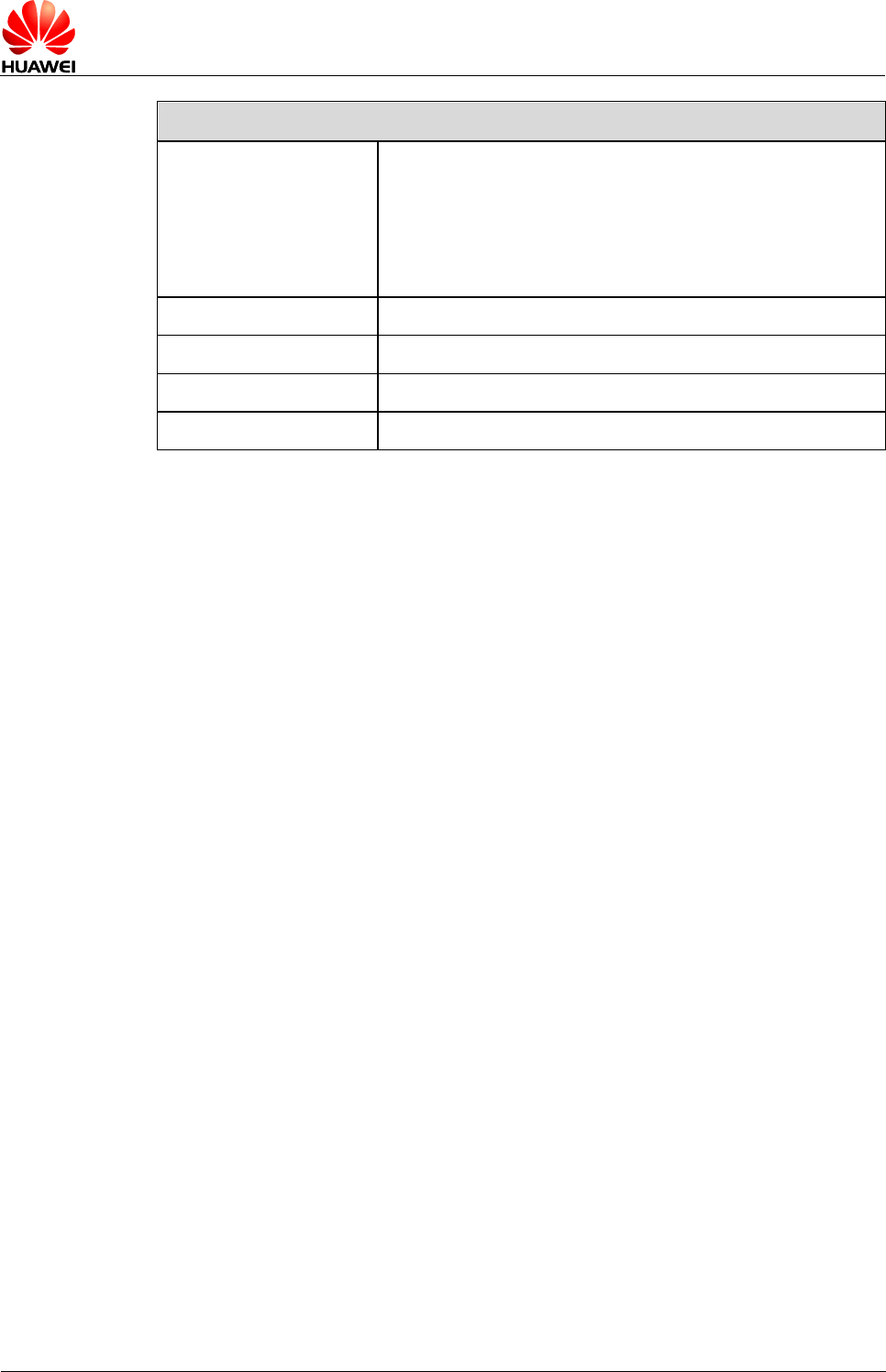
HUAWEI MU739 HSPA+ LGA Module
Hardware Guide
RF Specifications
Issue 11 (2015-10-08)
Huawei Proprietary and Confidential
Copyright © Huawei Technologies Co., Ltd.
46
GSM/WCDMA Antenna Requirements
Bandwidth of diversity
antenna
60 MHz in WCDMA Band 1
60 MHz in WCDMA Band 2
45 MHz in WCDMA Band 4
25 MHz in WCDMA Band 5
35 MHz in WCDMA Band 8
Gain
≤ 2.5 dBi
Impedance
50 Ω
VSWR absolute max
≤ 3:1
VSWR recommended
≤ 2:1
HUAWEI MU739 HSPA+ LGA Module
Hardware Guide
Electrical and Reliability Features
Issue 11 (2015-10-08)
Huawei Proprietary and Confidential
Copyright © Huawei Technologies Co., Ltd.
47
5 Electrical and Reliability Features
5.1 About This Chapter
This chapter describes the electrical and reliability features of the interfaces in the
MU739 module, including:
- Absolute Ratings
- Operating and Storage Temperature and Humidity
- Power Supply Features
- Reliability Features
- EMC and ESD Features
5.2 Absolute Ratings
Table 5-1 lists the absolute ratings for the MU739 module. Using the MU739 module
beyond these conditions may result in permanent damage to the module.
Table 5-1 Absolute maximum ratings for the MU739 module
Symbol
Specification
Minimum
Value
Maximum
Value
Unit
VBAT
External power voltage
–0.3
4.5
V
VI
Data pin voltage
–0.3
3.6
V
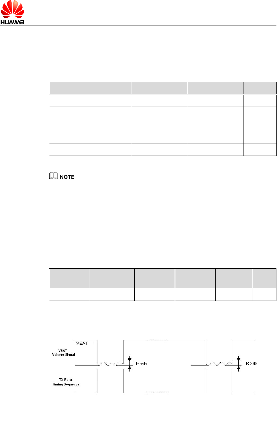
HUAWEI MU739 HSPA+ LGA Module
Hardware Guide
Electrical and Reliability Features
Issue 11 (2015-10-08)
Huawei Proprietary and Confidential
Copyright © Huawei Technologies Co., Ltd.
48
5.3 Operating and Storage Temperature and Humidity
Table 5-2 lists the operating and storage temperature and humidity for the MU739
module.
Table 5-2 Operating and storage temperature and humidity for the MU739 module
Specification
Minimum Value
Maximum Value
Unit
Normal working temperature
–10
+55
°C
Extreme working
temperature[1]
–20
+70
°C
Ambient temperature for
storage
–40
+85
°C
Humidity
5
95
%
[1]: When the MU739 module works from –20°C to –10°C or +55°C to +70°C , certain RF
performances do not comply with the 3GPP RF specifications.
5.4 Power Supply Features
5.4.1 Input Power Supply
Table 5-3 lists the requirements for input power of the MU739 module.
Table 5-3 Requirements for input power for the MU739 module
Parameter
Minimum
Value
Typical
Value
Maximum
Value
Ripple
Unit
VBAT
3.3
3.8
4.2
0.05
V
Figure 5-1 Power Supply During Burst Emission
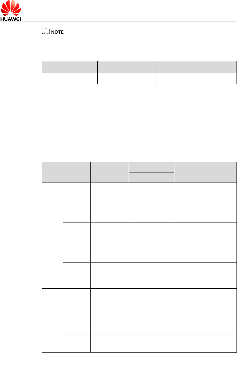
HUAWEI MU739 HSPA+ LGA Module
Hardware Guide
Electrical and Reliability Features
Issue 11 (2015-10-08)
Huawei Proprietary and Confidential
Copyright © Huawei Technologies Co., Ltd.
49
The VBAT Minimum Value must be guaranteed during the burst (with 2.75 A Peak in GSM,
GPRS or EGPRS mode).
Table 5-4 Requirements for input current of the MU739 module
Power
Peak (Maximum)
Normal (Maximum)
3.8 V
2750 mA
1100 mA
5.4.2 Power Consumption
The power consumptions of MU739 in different scenarios are respectively listed in
Table 5-5 , Table 5-6 and Table 5-7 .
The power consumption listed in this section are tested when the power supply of
MU739 module is normal voltage (3.8 V), and all of test values are measured at room
temperature.
Table 5-5 Averaged standby DC power consumption of MU739 (WCDMA/HSDPA/GSM)
Description
Bands
Test Value (mA)
Notes/Configuration
Typical
Sleep
HSPA+/
WCDMA
UMTS bands
1.9
Module is powered up.
DRX cycle=8 (2.56s)
Module is registered on
the network.
USB is in suspend.
GPRS/E
DGE
GSM bands
2.0
Module is powered up.
MFRMS=5 (1.175s)
Module is registered on
the network.
USB is in suspend.
Radio Off
All bands
1.4
Module is powered up.
RF is disabled.
USB is in suspend.
Idle
HSPA+/
WCDMA
UMTS bands
30
Module is powered up.
DRX cycle=8 (2.56s)
Module is registered on
the network, and no data
is transmitted.
USB is in active.
GPRS/E
DGE
GSM bands
30
Module is powered up.
MFRMS=5 (1.175s)
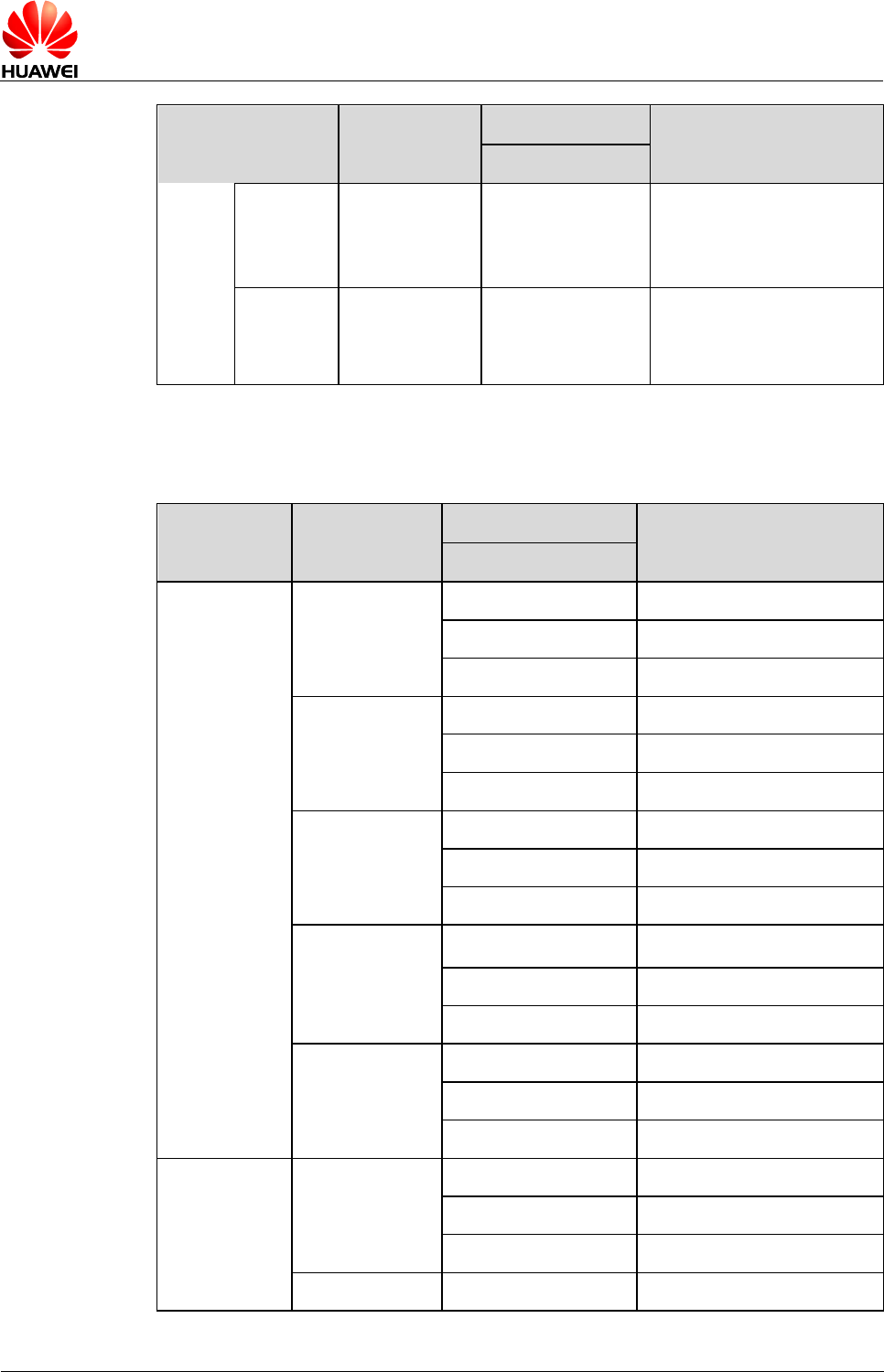
HUAWEI MU739 HSPA+ LGA Module
Hardware Guide
Electrical and Reliability Features
Issue 11 (2015-10-08)
Huawei Proprietary and Confidential
Copyright © Huawei Technologies Co., Ltd.
50
Description
Bands
Test Value (mA)
Notes/Configuration
Typical
Module is registered on
the network, and no data
is transmitted.
USB is in active.
Radio Off
All bands
30
Module is powered up.
RF is disabled.
USB is in active.
Table 5-6 Averaged Data Transmission DC power consumption of MU739
(WCDMA/HSPA+)
Description
Band
Test Value (mA)
Notes/Configuration
Typical
WCDMA
Band 1
(IMT2100)
175
0 dBm Tx Power
215
10 dBm Tx Power
570
23.5 dBm Tx Power
Band 2
(PCS 1900)
175
0 dBm Tx Power
220
10 dBm Tx Power
700
23.5 dBm Tx Power
Band 4
(AWS)
170
0 dBm Tx Power
210
10 dBm Tx Power
600
23.5 dBm Tx Power
Band 5
(850 MHz)
170
0 dBm Tx Power
205
10 dBm Tx Power
560
23.5 dBm Tx Power
Band 8
(900 MHz)
165
0 dBm Tx Power
205
10 dBm Tx Power
600
23.5 dBm Tx Power
HSPA+
Band 1
(IMT2100)
190
0 dBm Tx Power
230
10 dBm Tx Power
700
23.5 dBm Tx Power
Band 2
197
0 dBm Tx Power
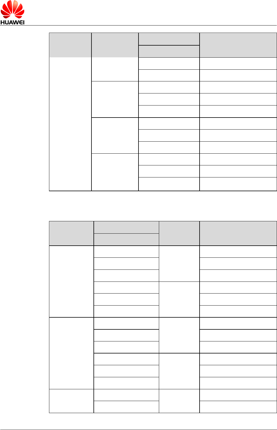
HUAWEI MU739 HSPA+ LGA Module
Hardware Guide
Electrical and Reliability Features
Issue 11 (2015-10-08)
Huawei Proprietary and Confidential
Copyright © Huawei Technologies Co., Ltd.
51
Description
Band
Test Value (mA)
Notes/Configuration
Typical
(PCS 1900)
240
10 dBm Tx Power
720
23.5 dBm Tx Power
Band 4
(AWS)
195
0 dBm Tx Power
230
10 dBm Tx Power
620
23.5 dBm Tx Power
Band 5
(850 MHz)
191
0 dBm Tx Power
220
10 dBm Tx Power
600
23.5 dBm Tx Power
Band 8
(900 MHz)
190
0 dBm Tx Power
225
10 dBm Tx Power
625
23.5 dBm Tx Power
Table 5-7 Averaged DC power consumption of MU739 (GPRS/EDGE)
Description
Test Value (mA)
PCL
Notes/Configuration
Typical
GPRS850
230
5
1 Up/1 Down
395
2 Up/1 Down
650
4 Up/1 Down
95
10
1 Up/1 Down
125
2 Up/1 Down
165
4 Up/1 Down
GPRS900
225
5
1 Up/1 Down
390
2 Up/1 Down
620
4 Up/1 Down
95
10
1 Up/1 Down
125
2 Up/1 Down
165
4 Up/1 Down
GPRS1800
190
0
1 Up/1 Down
310
2 Up/1 Down
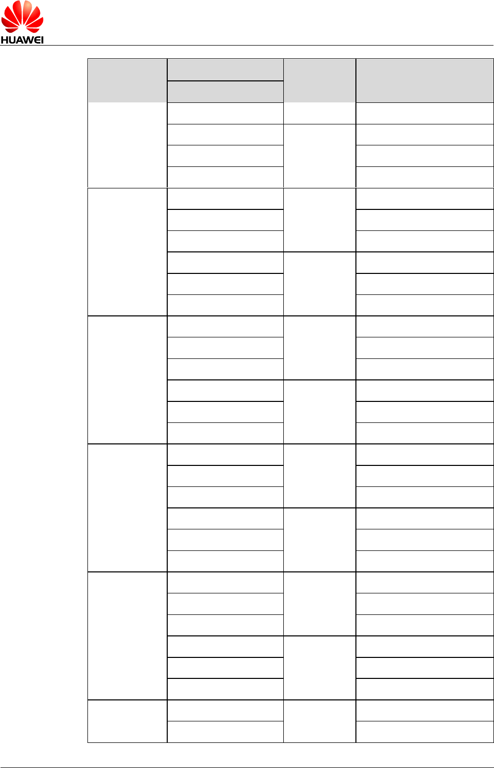
HUAWEI MU739 HSPA+ LGA Module
Hardware Guide
Electrical and Reliability Features
Issue 11 (2015-10-08)
Huawei Proprietary and Confidential
Copyright © Huawei Technologies Co., Ltd.
52
Description
Test Value (mA)
PCL
Notes/Configuration
Typical
410
4 Up/1 Down
90
10
1 Up/1 Down
110
2 Up/1 Down
145
4 Up/1 Down
GPRS1900
180
0
1 Up/1 Down
295
2 Up/1 Down
410
4 Up/1 Down
90
10
1 Up/1 Down
110
2 Up/1 Down
145
4 Up/1 Down
EDGE850
175
8
1 Up/1 Down
285
2 Up/1 Down
460
4 Up/1 Down
120
15
1 Up/1 Down
175
2 Up/1 Down
270
4 Up/1 Down
EDGE900
175
8
1 Up/1 Down
280
2 Up/1 Down
445
4 Up/1 Down
120
15
1 Up/1 Down
175
2 Up/1 Down
265
4 Up/1 Down
EDGE1800
160
2
1 Up/1 Down
260
2 Up/1 Down
415
4 Up/1 Down
110
10
1 Up/1 Down
155
2 Up/1 Down
230
4 Up/1 Down
EDGE1900
155
2
1 Up/1 Down
250
2 Up/1 Down
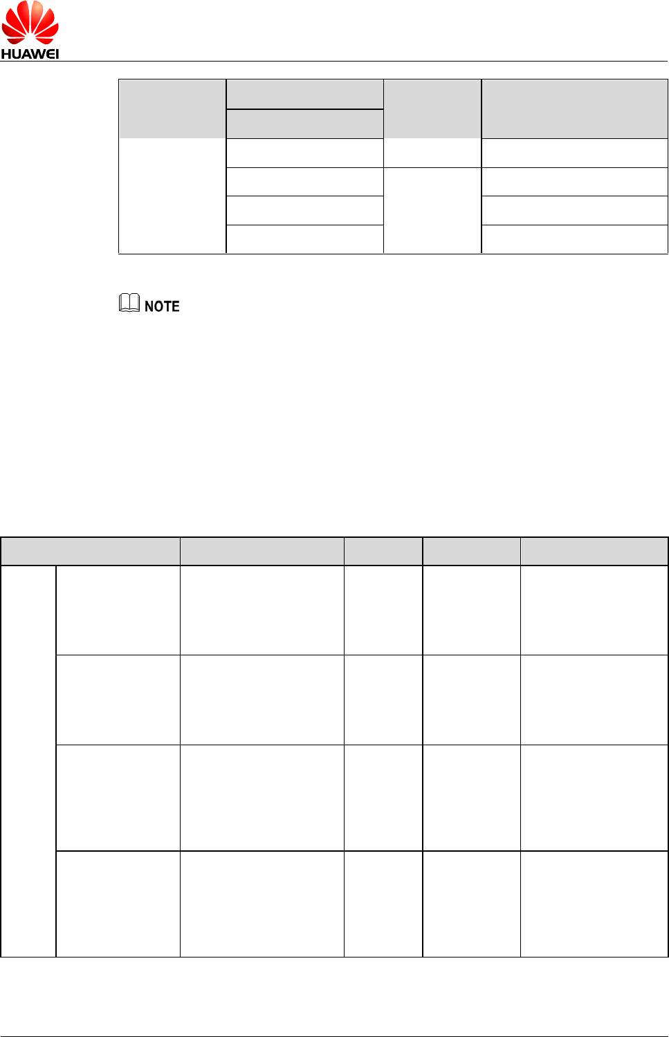
HUAWEI MU739 HSPA+ LGA Module
Hardware Guide
Electrical and Reliability Features
Issue 11 (2015-10-08)
Huawei Proprietary and Confidential
Copyright © Huawei Technologies Co., Ltd.
53
Description
Test Value (mA)
PCL
Notes/Configuration
Typical
410
4 Up/1 Down
110
10
1 Up/1 Down
155
2 Up/1 Down
230
4 Up/1 Down
- All power consumption test configuration can be referenced by GSM Association Official
Document TS.09: Battery Life Measurement and Current Consumption Technique.
- Test condition: For Max Tx power, see 4.4.2 Conducted Transmit Power, they are listed in
Table 4-3 ; for Max data throughput, see 2.2 Function Overview, they are listed in Table 2-1
Features.
5.5 Reliability Features
Table 5-8 lists the test conditions and results of the reliability of the MU739 module.
Table 5-8 Test conditions and results of the reliability of the MU739 module
Item
Test Condition
Standard
Sample size
Results
Stress
Low-temperature
storage
- Temperature: –40ºC
- Operation mode: no
power, no package
- Test duration: 24 h
JESD22-
A119-C
3 pcs/group
Visual inspection: ok
Function test: ok
RF specification: ok
High-temperature
storage
- Temperature: 85ºC
- Operation mode: no
power, no package
- Test duration: 24 h
JESD22-
A103-C
3 pcs/group
Visual inspection: ok
Function test: ok
RF specification: ok
Low-temperature
operating
- Temperature: –20ºC
- Operation mode:
working with service
connected
- Test duration: 24 h
IEC60068
-2-1
3 pcs/group
Visual inspection: ok
Function test: ok
RF specification: ok
High-temperature
operating
- Temperature: 70ºC
- Operation mode:
working with service
connected
- Test duration: 24 h
JESD22-
A108-C
3 pcs/group
Visual inspection: ok
Function test: ok
RF specification: ok
HUAWEI MU739 HSPA+ LGA Module
Hardware Guide
Electrical and Reliability Features
Issue 11 (2015-10-08)
Huawei Proprietary and Confidential
Copyright © Huawei Technologies Co., Ltd.
54
Item
Test Condition
Standard
Sample size
Results
Damp heat
cycling
- High temperature:
55ºC
- Low temperature:
25ºC
- Humidity: 95%±3%
- Operation mode:
working with service
connected
- Test duration: 6
cycles; 12 h+12
h/cycle
JESD22-
A101-B
3 pcs/group
Visual inspection: ok
Function test: ok
RF specification: ok
Thermal shock
- Low temperature:
–40ºC
- High temperature:
85ºC
- Temperature change
interval: < 20s
- Operation mode: no
power
- Test duration: 100
cycles; 15 min+15
min/cycle
JESD22-
A106-B
3 pcs/group
Visual inspection: ok
Function test: ok
RF specification: ok
Salty fog test
- Temperature: 35°C
- Density of the NaCl
solution: 5%±1%
- Operation mode: no
power, no package
- Test duration:
Spraying interval: 8 h
Exposing period after
removing the salty fog
environment: 16 h
JESD22-
A107-B
3 pcs/group
Visual inspection: ok
Function test: ok
RF specification: ok
Sine vibration
- Frequency range: 5
Hz to 200 Hz
- Acceleration: 1 Grms
- Frequency scan rate:
0.5 oct/min
- Operation mode:
working with service
connected
- Test duration: 3 axial
directions. 2 h for
each axial direction.
JESD22-
B103-B
3 pcs/group
Visual inspection: ok
Function test: ok
RF specification: ok
HUAWEI MU739 HSPA+ LGA Module
Hardware Guide
Electrical and Reliability Features
Issue 11 (2015-10-08)
Huawei Proprietary and Confidential
Copyright © Huawei Technologies Co., Ltd.
55
Item
Test Condition
Standard
Sample size
Results
Shock test
- Half-sine wave shock
- Peak acceleration: 30
Grms
- Shock duration: 11 ms
- Operation mode:
working with service
connected
- Test duration: 6 axial
directions. 3 shocks
for each axial
direction.
JESD-B1
04-C
3 pcs/group
Visual inspection: ok
Function test: ok
RF specification: ok
Drop test
- 0.8 m in height. Drop
the module on the
marble terrace with
one surface facing
downwards, six
surfaces should be
tested.
- Operation mode: no
power, no package
IEC60068
-2-32
3 pcs/group
Visual inspection: ok
Function test: ok
RF specification: ok
Life
High temperature
operating life
- Temperature: 70ºC
- Operation mode:
working with service
connected
- Test duration: 168 h,
336 h, 500 h, 1000 h
for inspection point
JESD22-
A108-B
50 pcs/group
Visual inspection: ok
Function test: ok
RF specification: ok
High temperature
& high humidity
- High temperature:
85ºC
- Humidity: 85%
- Operation mode:
powered on and no
working
- Test duration: 168 h,
336 h, 500 h, 1000 h
for inspection point
JESD22-
A110-B
50 pcs/group
Visual inspection: ok
Function test: ok
RF specification: ok
Cross section: ok
HUAWEI MU739 HSPA+ LGA Module
Hardware Guide
Electrical and Reliability Features
Issue 11 (2015-10-08)
Huawei Proprietary and Confidential
Copyright © Huawei Technologies Co., Ltd.
56
Item
Test Condition
Standard
Sample size
Results
Temperature
cycle
- High temperature:
85ºC
- Low temperature:
–40ºC
- Temperature change
slope: 6ºC/min
- Operation mode: no
power
- Test duration: 168 h,
336 h, 500 h, 1000 h
for inspection point
JESD22-
A104-C
50 pcs/group
Visual inspection: ok
Function test: ok
RF specification: ok
Cross section: ok
ESD
HBM (Human
Body Model)
- 1 kV (Class 1 B)
- Operation mode: no
power
JESD22-
A114-D
3 pcs/group
Visual inspection: ok
Function test: ok
RF specification: ok
ESD with DVK (or
embedded in the
host)
- Contact Voltage: ±2
kV, ±4 kV
- Air Voltage : ±2 kV, ±4
kV, ±8 kV
- Operation mode:
working with service
connected
IEC61000
-4-2
2 pcs
Visual inspection: ok
Function test: ok
RF specification: ok
Groups ≥ 2
5.6 EMC and ESD Features
The following are the EMC design comments:
- Attention should be paid to static control in the manufacture, assembly, packaging,
handling, and storage process to reduce electrostatic damage to HUAWEI
module.
- RSE (Radiated Spurious Emission) may exceed the limit defined by EN301489 if
the antenna port is protected by TVS (Transient Voltage Suppressor), which is
resolved by making some adjustments on RF match circuit.
- TVS should be added on the USB port for ESD protection, and the parasitic
capacitance of TVS on D+/D- signal should be less than 2 pF. Common-mode
inductor should be added in parallel on D+/D- signal.
- TVS should be added on the USIM interface for ESD protection. The parasitic
capacitance of TVS on USIM signal should be less than 10 pF.

HUAWEI MU739 HSPA+ LGA Module
Hardware Guide
Electrical and Reliability Features
Issue 11 (2015-10-08)
Huawei Proprietary and Confidential
Copyright © Huawei Technologies Co., Ltd.
57
- Resistors in parallel and a 10 nF capacitor should be added on RESET_BB_N
signal to avoid shaking, and the distance between the capacitor and the related
pin should be less than 100 mil.
- PCB routing should be V-type rather than T-type for TVS.
- An integrated ground plane is necessary for EMC design.
The following are the requirements of ESD environment control:
- The electrostatic discharge protected area (EPA) must have an ESD floor whose
surface resistance and system resistance are greater than 1 x 10⁴ Ω while less
than 1 x 10⁹ Ω.
- The EPA must have a sound ground system without loose ground wires, and the
ground resistance must be less than 4 Ω.
- The workbench for handling ESD sensitive components must be equipped with
common ground points, the wrist strap jack, and ESD pad. The resistance
between the jack and common ground point must be less than 4 Ω. The surface
resistance and system resistance of the ESD pad must be less than 1 x 10⁹ Ω.
- The EPA must use the ESD two-circuit wrist strap, and the wrist strap must be
connected to the dedicated jack. The crocodile clip must not be connected to the
ground.
- The ESD sensitive components, the processing equipment, test equipment, tools,
and devices must be connected to the ground properly. The indexes are as
follows:
− Hard ground resistance < 4 Ω
− 1 x 10⁵ Ω ≤ Soft ground resistance < 1 x 10⁹ Ω
− 1 x 10⁵ Ω ≤ ICT fixture soft ground resistance < 1 x 10¹¹ Ω
− The electronic screwdriver and electronic soldering iron can be easily oxidized.
Their ground resistance must be less than 20 Ω.
- The parts of the equipment, devices, and tools that touch the ESD sensitive
components and moving parts that are close to the ESD sensitive components
must be made of ESD materials and have sound ground connection. The parts
that are not made of ESD materials must be handled with ESD treatment, such
as painting the ESD coating or ionization treatment (check that the friction voltage
is less than 100 V).
- Key parts in the production equipment (parts that touch the ESD sensitive
components or parts that are within 30 cm away from the ESD sensitive
components), including the conveyor belt, conveyor chain, guide wheel, and SMT
nozzle, must all be made of ESD materials and be connected to the ground
properly (check that the friction voltage is less than 100 V).
- Engineers that touch IC chips, boards, modules, and other ESD sensitive
components and assemblies must wear ESD wrist straps, ESD gloves, or ESD
finger cots properly. Engineers that sit when handling the components must all
wear ESD wrist straps.
- Noticeable ESD warning signs must be attached to the packages and placement
areas of ESD sensitive components and assemblies.
- Boards and IC chips must not be stacked randomly or be placed with other ESD
components.
- Effective shielding measures must be taken on the ESD sensitive materials that
are transported or stored outside the EPA.

HUAWEI MU739 HSPA+ LGA Module
Hardware Guide
Electrical and Reliability Features
Issue 11 (2015-10-08)
Huawei Proprietary and Confidential
Copyright © Huawei Technologies Co., Ltd.
58
HUAWEI MU739 Module does not include any protection against overvoltage.

HUAWEI MU739 HSPA+ LGA Module
Hardware Guide
Process Design
Issue 11 (2015-10-08)
Huawei Proprietary and Confidential
Copyright © Huawei Technologies Co., Ltd.
59
6 Process Design
6.1 About This Chapter
This chapter describes the process design and mechanical specifications:
- Storage Requirement
- Moisture Sensitivity
- Dimensions
- Packaging
- Label
- Customer PCB Design
- Thermal Design Solution
- Assembly Processes
- Specification of Rework
6.2 Storage Requirement
The module must be stored and sealed properly in vacuum package under a
temperature below 40°C and the relative humidity less than 90% in order to ensure
the weldability within 12 months.
6.3 Moisture Sensitivity
- The moisture sensitivity is level 3.
- After unpacking, the module must be assembled within 168 hours under the
environmental conditions that the temperature is lower than 30°C and the relative
humidity is less than 60%. If the preceding conditions cannot be met, the module
needs to be baked according to the parameters specified in Table 6-1 .
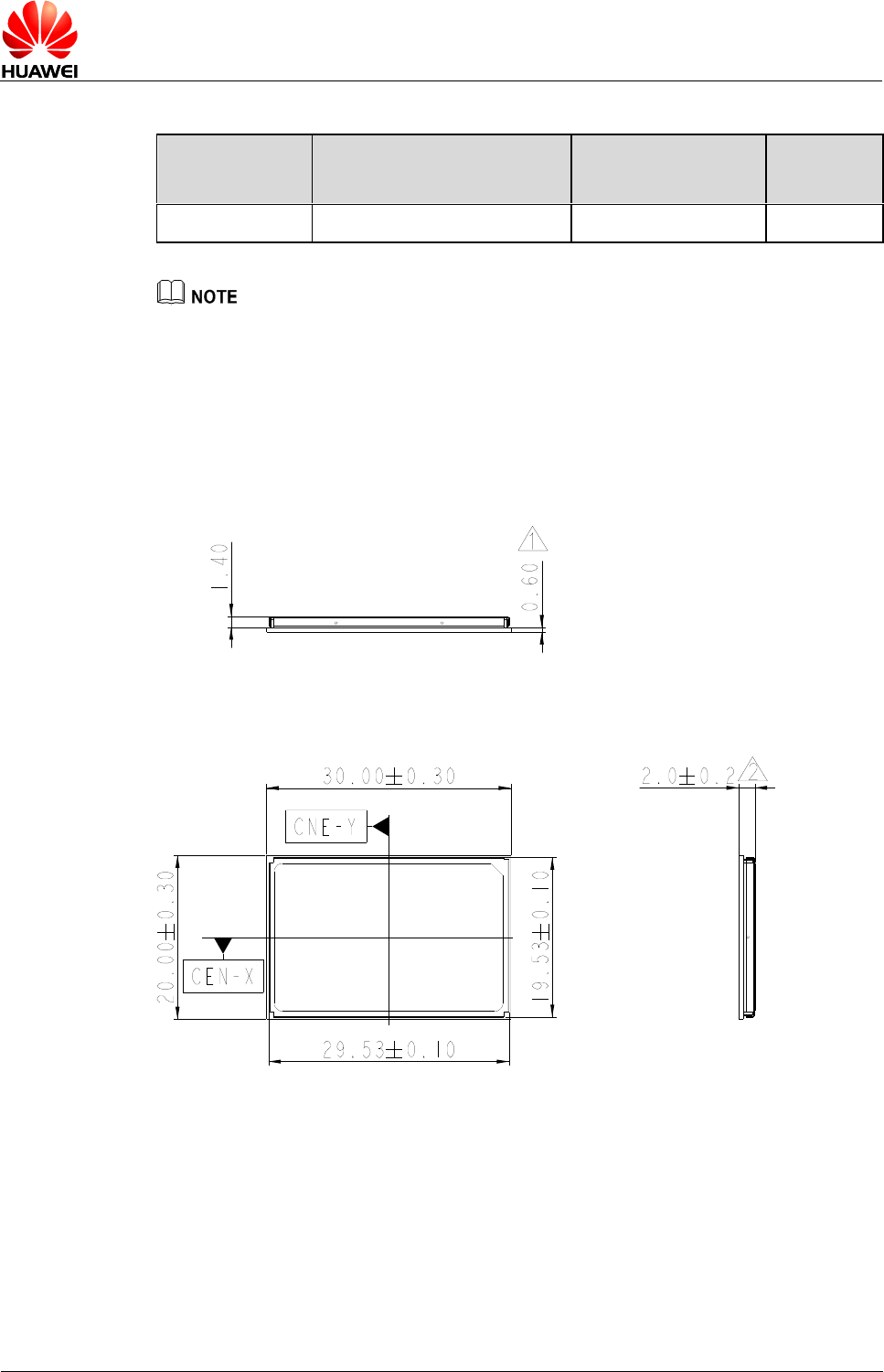
HUAWEI MU739 HSPA+ LGA Module
Hardware Guide
Process Design
Issue 11 (2015-10-08)
Huawei Proprietary and Confidential
Copyright © Huawei Technologies Co., Ltd.
60
Table 6-1 Baking parameters
Baking
Temperature
Baking Condition
Baking Duration
Remarks
125°C ±5°C
Relative humidity ≤ 60%
8 hours
-
Moving, storing, and processing the product must comply with IPC/JEDEC J-STD-033.
6.4 Dimensions
Figure 6-1 shows the dimensions of MU739 in details.
Figure 6-1 Dimensions (Unit: mm)
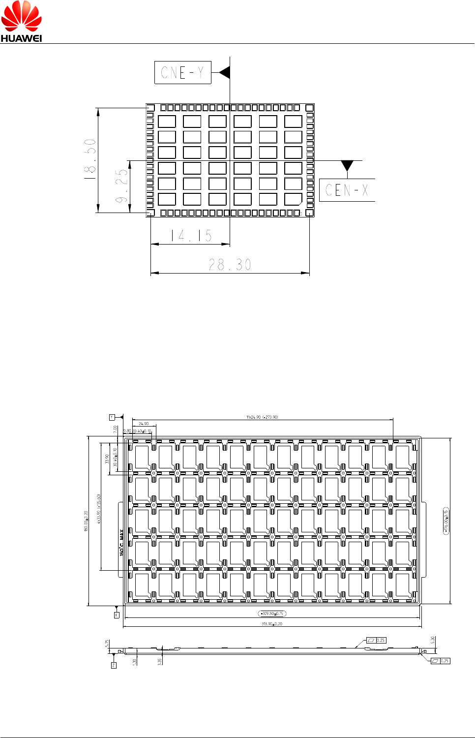
HUAWEI MU739 HSPA+ LGA Module
Hardware Guide
Process Design
Issue 11 (2015-10-08)
Huawei Proprietary and Confidential
Copyright © Huawei Technologies Co., Ltd.
61
6.5 Packaging
The module uses five layers ESD pallet, anti-vibration foam and vacuum packing into
cartons.
Figure 6-2 ESD pallet (Unit: mm)
The following figure shows the packaging.
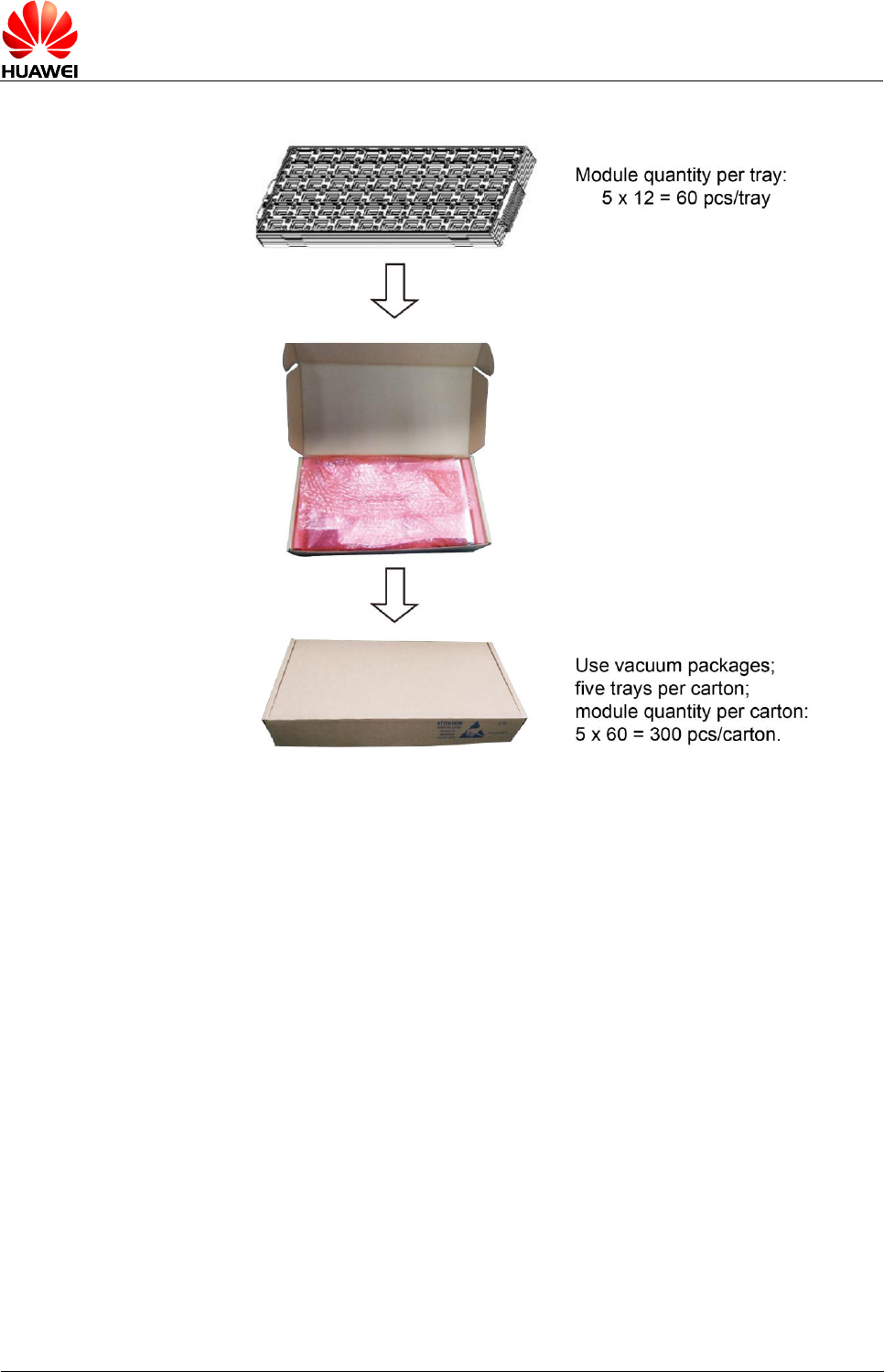
HUAWEI MU739 HSPA+ LGA Module
Hardware Guide
Process Design
Issue 11 (2015-10-08)
Huawei Proprietary and Confidential
Copyright © Huawei Technologies Co., Ltd.
62
Figure 6-3 Description of the packaging
6.6 Label
The label is made from deformation-resistant, fade-resistant, and
high-temperature-resistant material and is able to endure the high temperature of
260°C .
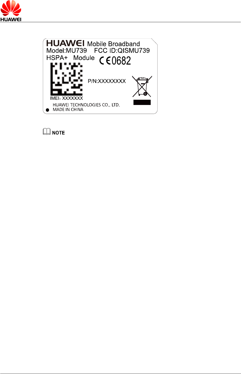
HUAWEI MU739 HSPA+ LGA Module
Hardware Guide
Process Design
Issue 11 (2015-10-08)
Huawei Proprietary and Confidential
Copyright © Huawei Technologies Co., Ltd.
63
Figure 6-4 MU739 label
The picture mentioned above is only for reference.
6.7 Customer PCB Design
6.7.1 PCB Surface Finish
The PCB surface finish recommended is Electroless Nickel, immersion Gold (ENIG).
Organic Solderability Preservative (OSP) may also be used, ENIG preferred.
6.7.2 PCB Pad Design
To achieve assembly yields and solder joints of high reliability, it is recommended that
the PCB pad size be designed as follows:
The sizes of the solder pads on customers' PCBs are the same as those of the
module package's solder pads. For details, see the following figure.
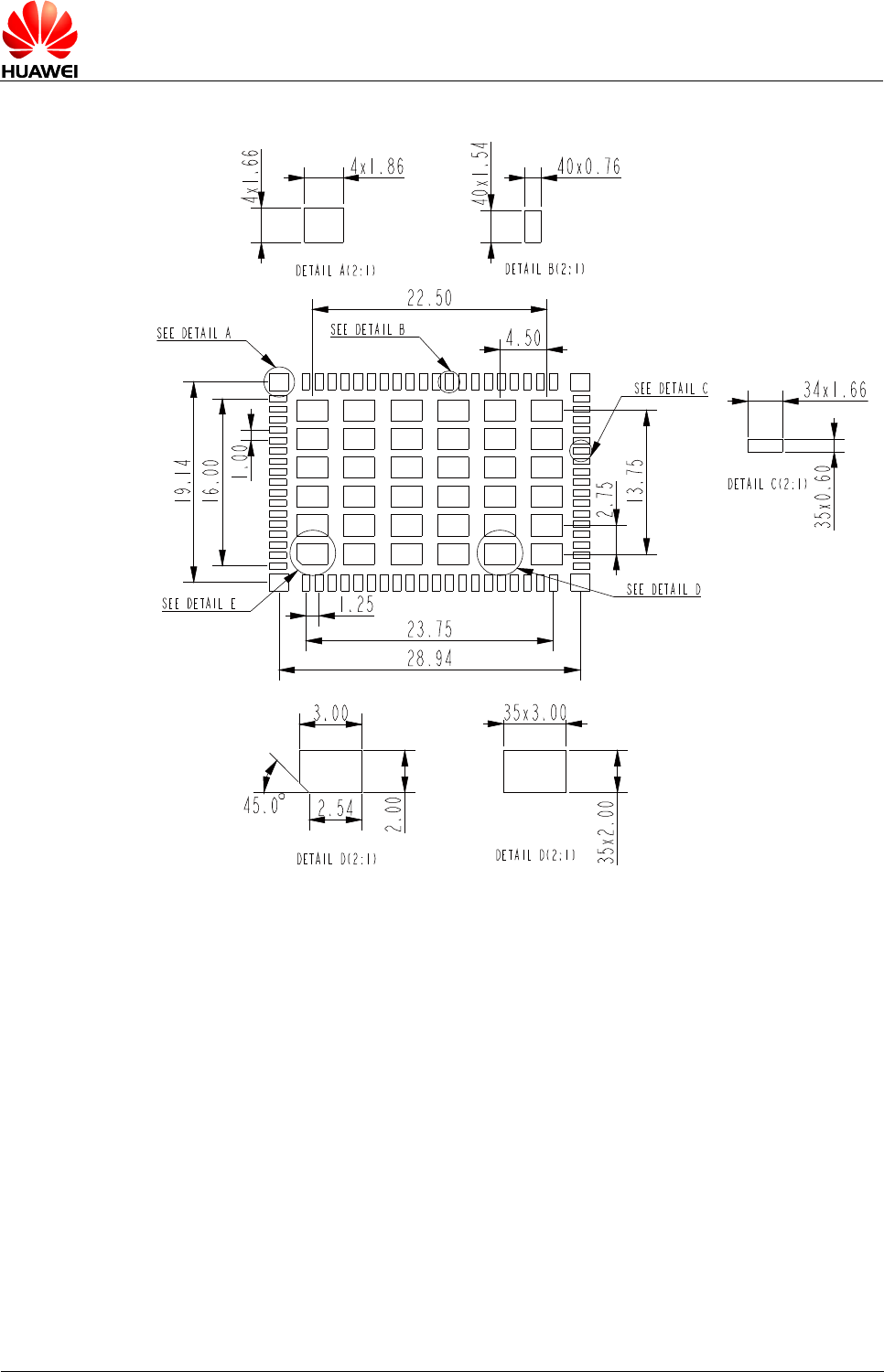
HUAWEI MU739 HSPA+ LGA Module
Hardware Guide
Process Design
Issue 11 (2015-10-08)
Huawei Proprietary and Confidential
Copyright © Huawei Technologies Co., Ltd.
64
Figure 6-5 PCB pad design (Top View) (Unit: mm)
6.7.3 Solder Mask
NSMD is recommended. In addition, the solder mask of the NSMD pad design is
larger than the pad so the reliability of the solder joint can be improved.
The solder mask must be 100 µm–150 µm larger than the pad, that is, the single side
of the solder mask must be 50 µm–75 µm larger than the pad. The specific size
depends on the processing capability of the PCB manufacturer.
6.7.4 Requirements on PCB Layout
- To reduce deformation, a thickness of at least 1.0 mm is recommended.
- Other devices must be located more than 3 mm (5 mm recommended) away from
the two parallel sides of the LGA module (rework requirement),and other sides
with 0.6 mm. The minimum distance between the LGA module and the PCB edge
is 0.3 mm.
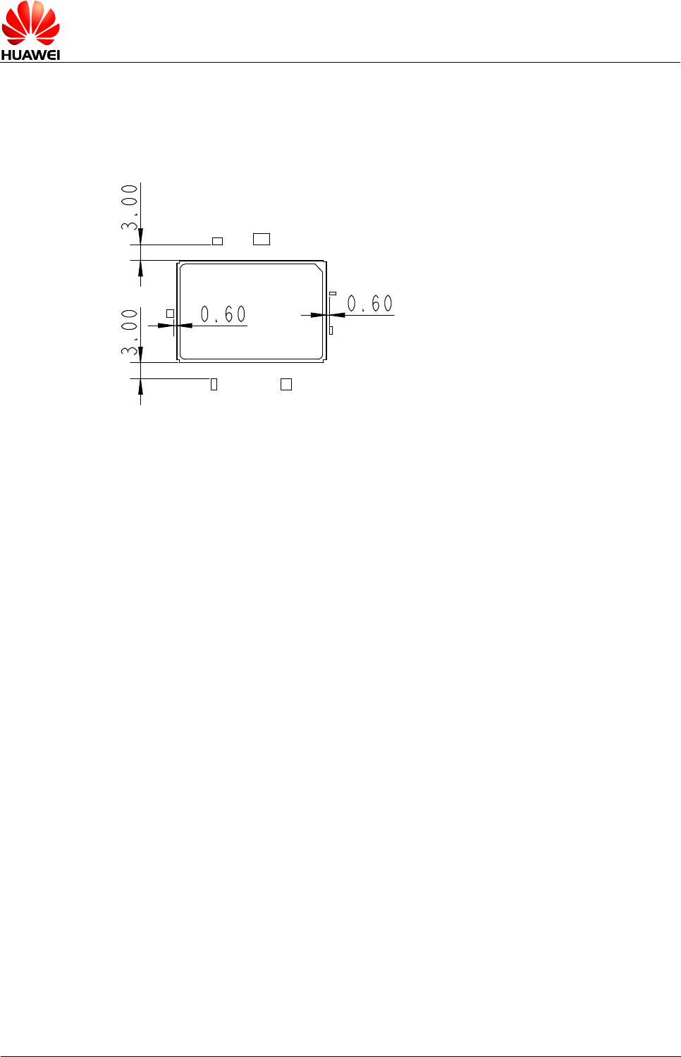
HUAWEI MU739 HSPA+ LGA Module
Hardware Guide
Process Design
Issue 11 (2015-10-08)
Huawei Proprietary and Confidential
Copyright © Huawei Technologies Co., Ltd.
65
- When the PCB layout is double sided, the LGA module must be placed on the
second side for assembly; so as to avoid module dropped from PCB or
component (located in module) re-melding defects caused by uneven weight.
Figure 6-6 PCB Layout (unit: mm)
6.8 Thermal Design Solution
When the module works in the maximum power condition, the module has high power
consumption (for details, see 5.4.2 Power Consumption). To improve the module
reliability and stability, focus on the thermal design of the device to speed up heat
dissipation. For thermal characteristics of the MU739 module, you can refer to 5.3
Operating and Storage Temperature and Humidity.
Take the following heat dissipation measures:
- The copper size on the PCB should be 70 mm x 70 mm or larger.
- All copper ground layers of the PCB must be connected to each other through
via-holes.
- Increase the quantity of the PCB ground planes.
- The ground planes should be as continuous as possible.
- If a fan is deployed, place the module at the cold air inlet.
- Use heat sink, thermal conductive material and product enclosure to enhance the
heat dissipation of the module.
− Use anodized heat sink on the shielding case or the customer PCB on bottom
side for optimal heat dissipation. The recommended heat sink dimensions are
70 mm x 70 mm x1 mm or larger.
− The material of the heat sink should adopt the higher thermal conductivity
metallic materials, e.g. Al or Cu.
− The recommended thermal conductivity of the thermal conductive material is
1.0 W/m-k or higher (recommended manufacturers: Laird or Bergquist).
− Conductive material should obey the following rule: after the heat sink is
fastened to the shielding case, the compression amount of the thermal
conductive material accounts for 15% to 30% of the thermal conductive
material size.
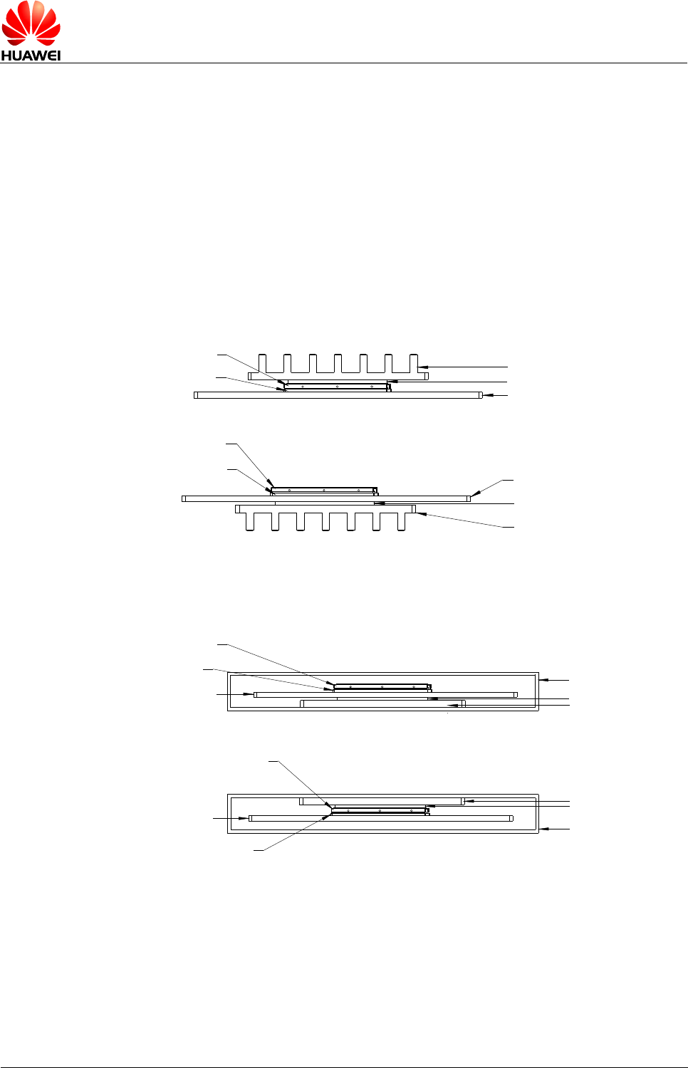
HUAWEI MU739 HSPA+ LGA Module
Hardware Guide
Process Design
Issue 11 (2015-10-08)
Huawei Proprietary and Confidential
Copyright © Huawei Technologies Co., Ltd.
66
− Conductive material should be as thin as possible.
− The recommended material of the enclosure is metallic materials, especially
you can add pin fin on the enclosure surface.
− If the heat sink is installed above the shielding case, you should attach the
thermal conductive material between the shielding case and the heat sink; if
the heat sink is installed below the bottom side of the customer PCB, you
should attach the thermal conductive material between the customer PCB and
the heat sink, as shown in Figure 6-7 and Figure 6-8 . Preferably, we
recommend the heat sink be installed below the bottom side of the customer
PCB.
− Use more pin fins to enlarge heat dissipation area.
Figure 6-7 Adding heat sink to the module for optimal heat dissipation
Module PCB Heat sink
Conductive material
Customer PCB
Module PCB
Heat sink
Conductive material
Customer PCB
Shielding case
Shielding case
Figure 6-8 Adding enclosure to enhance the heat dissipation of the module
Module PCB
Heat sink
Conductive material
Customer PCB Enclosure
Shielding case
Heat sink
Conductive material
Customer PCB Enclosure
Module PCB
Shielding case
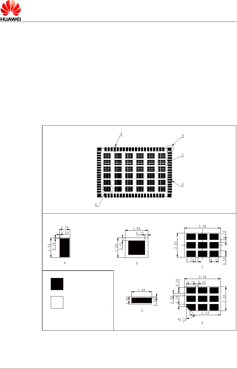
HUAWEI MU739 HSPA+ LGA Module
Hardware Guide
Process Design
Issue 11 (2015-10-08)
Huawei Proprietary and Confidential
Copyright © Huawei Technologies Co., Ltd.
67
6.9 Assembly Processes
6.9.1 General Description of Assembly Processes
- Tray modules are required at SMT lines, because the module is placed on ESD
pallets.
- Reflow ovens with at least seven temperature zones are recommended.
- Only twice reflow are allowed. Use reflow ovens or rework stations for soldering,
because the module has large solder pads and cannot be soldered manually.
6.9.2 Stencil Design
It is recommended that the stencil for the module be 0.15 mm in thickness. For the
stencil design, see the following figure:
PCB PADS
Stencil design
Unit: mm
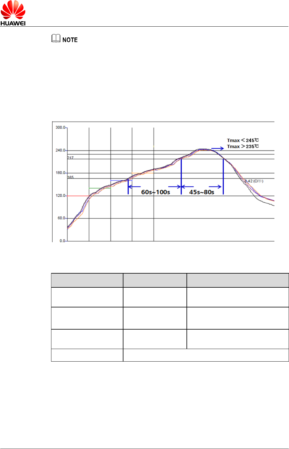
HUAWEI MU739 HSPA+ LGA Module
Hardware Guide
Process Design
Issue 11 (2015-10-08)
Huawei Proprietary and Confidential
Copyright © Huawei Technologies Co., Ltd.
68
The stencil design has been qualified for HUAWEI mainboard assembly, customers can adjust
the parameters by their motherboard design and process situation to assure LGA soldering
quality and no defect.
6.9.3 Reflow Profile
The LGA module must be reflowed on the top side of customer's development board.
For the soldering temperature of the LGA module, see the following figure.
Figure 6-9 Reflow profile
Table 6-2 Reflow parameters
Temperature Zone
Time
Key Parameter
Preheat zone
(40°C–165°C)
-
Heating rate: 0.5°C/s–2°C/s
Soak zone
(165°C–217°C)
(t1–t2): 60s–100s
-
Reflow zone (> 217°C)
(t3–t4): 45s–80s
Peak reflow temperature:
235°C –245°C
Cooling zone
Cooling rate: 2°C/s ≤ Slope ≤ 5°C/s
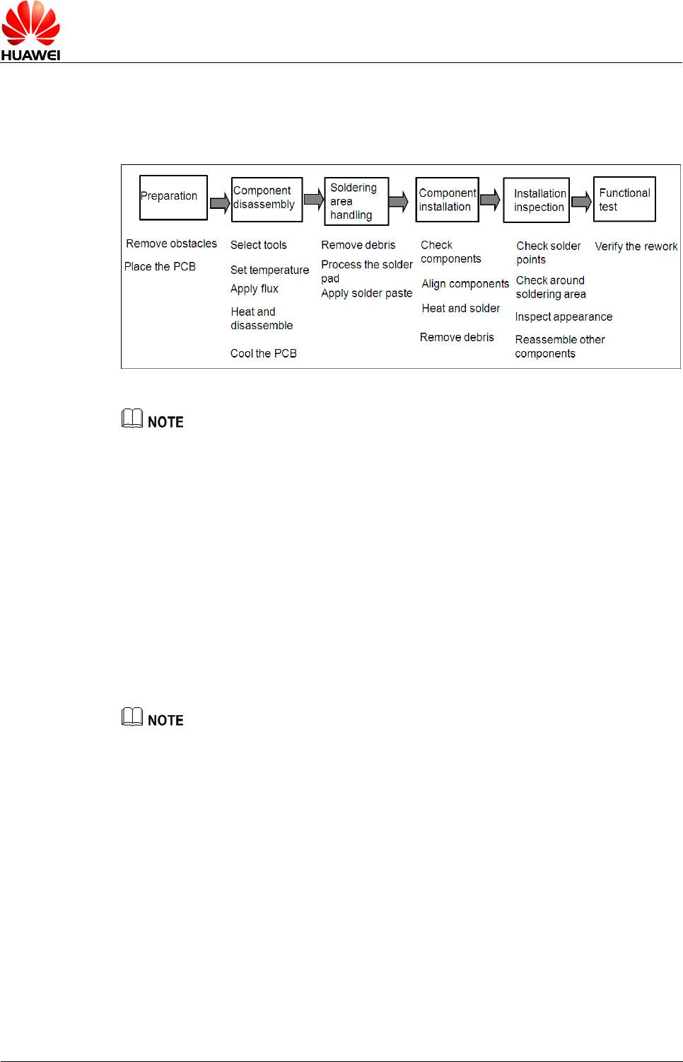
HUAWEI MU739 HSPA+ LGA Module
Hardware Guide
Process Design
Issue 11 (2015-10-08)
Huawei Proprietary and Confidential
Copyright © Huawei Technologies Co., Ltd.
69
6.10 Specification of Rework
6.10.1 Process of Rework
Huawei provides the rework scheme to assemble and remove the module. After the
rework, customers can evaluate the reliability based on their own requirement.
6.10.2 Preparations of Rework
- Remove barrier or devices that cannot stand high temperature before rework.
- If the device to be reworked is beyond the storage period, bake the device
according to Table 6-1 .
6.10.3 Removing the Module
The solder is molten and reflowed through heating during the module removing
process. The heating rate must be quick but controllable in order to melt all the solder
joints simultaneously. Pay attention to protect the module, PCB, neighboring devices,
and their solder joints against heating or mechanical damages.
- The module has many solder pads and the pads are large. Therefore, common soldering
irons and heat guns cannot be used in the rework. Rework must be done using either
infrared heating rework stations or hot air rework stations. Infrared heating rework stations
are preferred, because they can heat components without touching them. In addition,
infrared heating rework stations produce less solder debris and less impact on the module,
while hot air rework stations may cause shift of other components not to be reworked.
- You must not reuse the module after disassembly from PCB during rework.
- It is proposed that a special clamp is used to remove the module.
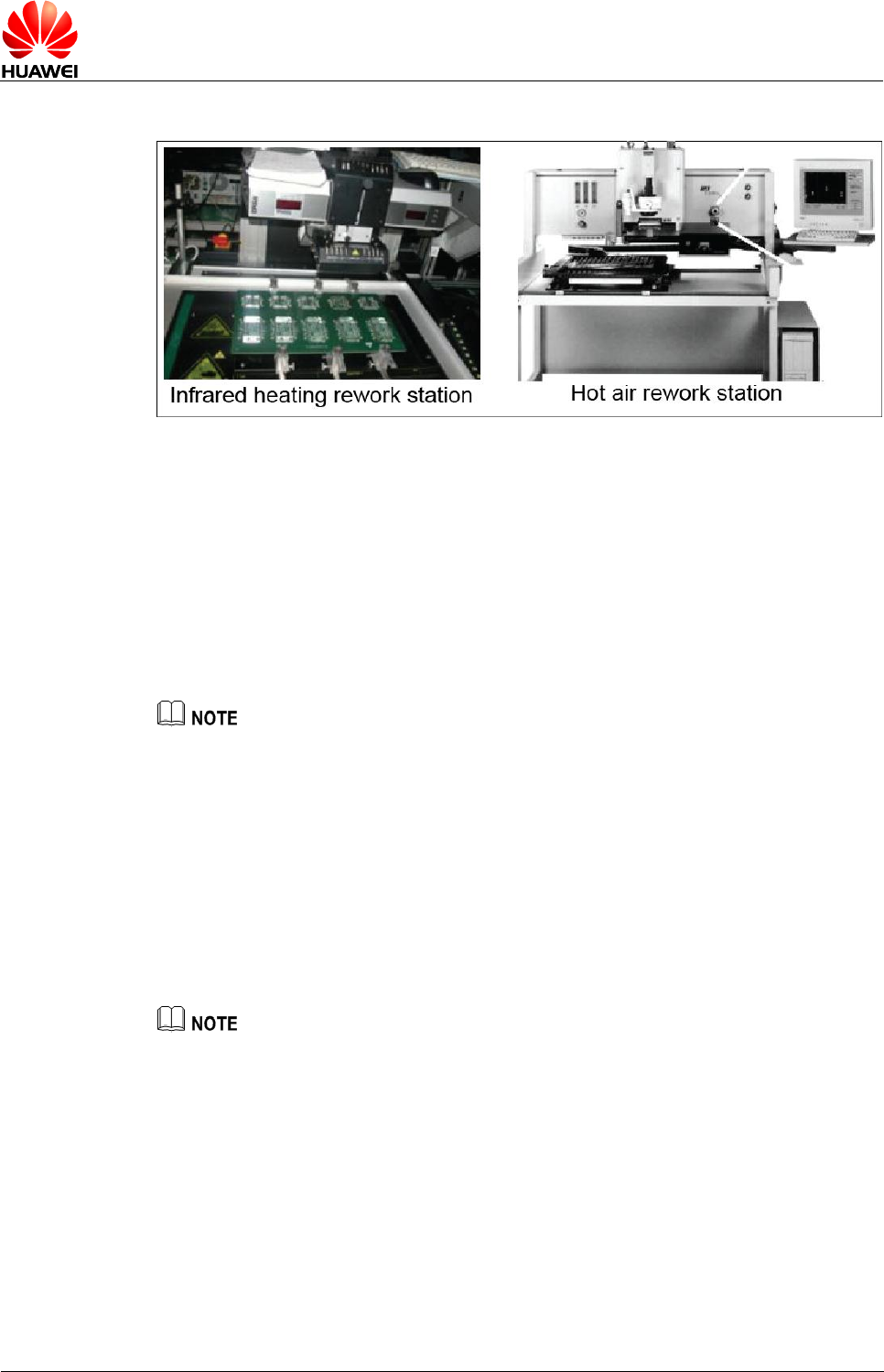
HUAWEI MU739 HSPA+ LGA Module
Hardware Guide
Process Design
Issue 11 (2015-10-08)
Huawei Proprietary and Confidential
Copyright © Huawei Technologies Co., Ltd.
70
Figure 6-10 Equipment used for rework
6.10.4 Welding Area Treatmtent
Step 1 Remove the old solder by using a soldering iron and solder braid that can wet the
solder.
Step 2 Clean the pad and remove the flux residuals.
Step 3 Solder pre-filling: Before the module is installed on a board, apply some solder paste
to the pad of the module by using the rework fixture and stencil or apply some solder
paste to the pad on the PCB by using a rework stencil.
It is recommended that a fixture and a mini-stencil be made to apply the solder paste in the
rework.
6.10.5 Module Installation
Install the module precisely on the module and ensure the right installation direction of
the module and the reliability of the electrical connection with the PCB. It is
recommended that the module be preheated in order to ensure that the temperature
of all parts to be soldered is uniform during the reflow process. The solder quickly
reflows upon heating so the parts are soldered reliably. The solder joints undergo
proper reflow duration at a preset temperature to form a favorable Intermetallic
Compound (IMC).
- It is recommended that a special clamp be used to pick the module when the module is
installed on the pad after applied with some solder.
- A special rework device must be used for the rework.
6.10.6 Specifications of Rework
Temperature parameter of rework: for either the removing or welding of the module,
the heating rate during the rework must be equal to or smaller than 3°C/s, and the
peak temperature between 240°C –250°C. The following parameters are
recommended during the rework.
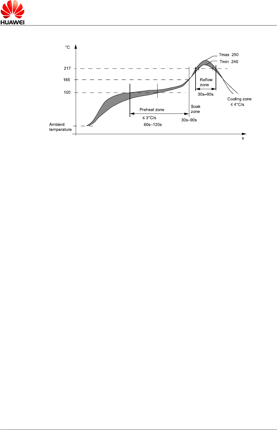
HUAWEI MU739 HSPA+ LGA Module
Hardware Guide
Process Design
Issue 11 (2015-10-08)
Huawei Proprietary and Confidential
Copyright © Huawei Technologies Co., Ltd.
71
Figure 6-11 Temperature graph of rework
HUAWEI MU739 HSPA+ LGA Module
Hardware Guide
Certifications
Issue 11 (2015-10-08)
Huawei Proprietary and Confidential
Copyright © Huawei Technologies Co., Ltd.
72
7 Certifications
7.1 About This Chapter
This chapter gives a general description of certifications of MU739.
7.2 Certifications
Table 7-1 shows certifications the MU739 has been implemented. For more demands, please
contact us for more details about this information.
Table 7-1 Product Certifications
Certification
Model name
MU739
CE
FCC
CCC
NCC
-
A-TICK
Jate & Telec
-
IC
-
EU RoHS
PVC-Free
-
GCF
PTCRB

HUAWEI MU739 HSPA+ LGA Module
Hardware Guide
Safety Information
Issue 11 (2015-10-08)
Huawei Proprietary and Confidential
Copyright © Huawei Technologies Co., Ltd.
73
8 Safety Information
Read the safety information carefully to ensure the correct and safe use of your
wireless device. Applicable safety information must be observed.
8.1 Interference
Power off your wireless device if using the device is prohibited. Do not use the
wireless device when it causes danger or interference with electric devices.
8.2 Medical Device
- Power off your wireless device and follow the rules and regulations set forth by
the hospitals and health care facilities.
- Some wireless devices may affect the performance of the hearing aids. For any
such problems, consult your service provider.
- Pacemaker manufacturers recommend that a minimum distance of 15 cm be
maintained between the wireless device and a pacemaker to prevent potential
interference with the pacemaker. If you are using an electronic medical device,
consult the doctor or device manufacturer to confirm whether the radio wave
affects the operation of this device.
8.3 Area with Inflammables and Explosives
To prevent explosions and fires in areas that are stored with inflammable and
explosive devices, power off your wireless device and observe the rules. Areas stored
with inflammables and explosives include but are not limited to the following:
- Gas station
- Fuel depot (such as the bunk below the deck of a ship)
- Container/Vehicle for storing or transporting fuels or chemical products
- Area where the air contains chemical substances and particles (such as granule,
dust, or metal powder)
- Area indicated with the "Explosives" sign

HUAWEI MU739 HSPA+ LGA Module
Hardware Guide
Safety Information
Issue 11 (2015-10-08)
Huawei Proprietary and Confidential
Copyright © Huawei Technologies Co., Ltd.
74
- Area indicated with the "Power off bi-direction wireless equipment" sign
- Area where you are generally suggested to stop the engine of a vehicle
8.4 Traffic Security
- Observe local laws and regulations while using the wireless device. To prevent
accidents, do not use your wireless device while driving.
- RF signals may affect electronic systems of motor vehicles. For more information,
consult the vehicle manufacturer.
- In a motor vehicle, do not place the wireless device over the air bag or in the air
bag deployment area. Otherwise, the wireless device may hurt you owing to the
strong force when the air bag inflates.
8.5 Airline Security
Observe the rules and regulations of airline companies. When boarding or
approaching a plane, power off your wireless device. Otherwise, the radio signal of
the wireless device may interfere with the plane control signals.
8.6 Safety of Children
Do not allow children to use the wireless device without guidance. Small and sharp
components of the wireless device may cause danger to children or cause suffocation
if children swallow the components.
8.7 Environment Protection
Observe the local regulations regarding the disposal of your packaging materials,
used wireless device and accessories, and promote their recycling.
8.8 WEEE Approval
The wireless device is in compliance with the essential requirements and other
relevant provisions of the Waste Electrical and Electronic Equipment Directive
2012/19/EU (WEEE Directive).
8.9 RoHS Approval
The wireless device is in compliance with the restriction of the use of certain
hazardous substances in electrical and electronic equipment Directive 2011/65/EU
(RoHS Directive).

HUAWEI MU739 HSPA+ LGA Module
Hardware Guide
Safety Information
Issue 11 (2015-10-08)
Huawei Proprietary and Confidential
Copyright © Huawei Technologies Co., Ltd.
75
8.10 Laws and Regulations Observance
Observe laws and regulations when using your wireless device. Respect the privacy
and legal rights of the others.
8.11 Care and Maintenance
It is normal that your wireless device gets hot when you use or charge it. Before you
clean or maintain the wireless device, stop all applications and power off the wireless
device.
- Use your wireless device and accessories with care and in clean environment.
Keep the wireless device from a fire or a lit cigarette.
- Protect your wireless device and accessories from water and vapour and keep
them dry.
- Do not drop, throw or bend your wireless device.
- Clean your wireless device with a piece of damp and soft antistatic cloth. Do not
use any chemical agents (such as alcohol and benzene), chemical detergent, or
powder to clean it.
- Do not leave your wireless device and accessories in a place with a considerably
low or high temperature.
- Use only accessories of the wireless device approved by the manufacture.
Contact the authorized service center for any abnormity of the wireless device or
accessories.
- Do not dismantle the wireless device or accessories. Otherwise, the wireless
device and accessories are not covered by the warranty.
- The device should be installed and operated with a minimum distance of 20 cm
between the radiator and your body.
8.12 Emergency Call
This wireless device functions through receiving and transmitting radio signals.
Therefore, the connection cannot be guaranteed in all conditions. In an emergency,
you should not rely solely on the wireless device for essential communications.
8.13 Regulatory Information
The following approvals and notices apply in specific regions as noted.
8.13.1 CE Approval (European Union)
The wireless device is approved to be used in the member states of the EU. The
wireless device is in compliance with the essential requirements and other relevant
provisions of the Radio and Telecommunications Terminal Equipment Directive
1999/5/EC (R&TTE Directive).

HUAWEI MU739 HSPA+ LGA Module
Hardware Guide
Safety Information
Issue 11 (2015-10-08)
Huawei Proprietary and Confidential
Copyright © Huawei Technologies Co., Ltd.
76
8.13.2 FCC Statement
Federal Communications Commission Notice (United States): Before a wireless
device model is available for sale to the public, it must be tested and certified to the
FCC that it does not exceed the limit established by the government-adopted
requirement for safe exposure.
This device complies with Part 15 of the FCC Rules. Operation is subject to the
following two conditions: (1) this device may not cause harmful interference, and (2)
this device must accept any interference received, including interference that may
cause undesired operation.
Warning: Changes or modifications made to this equipment not expressly approved
by HUAWEI may void the FCC authorization to operate this equipment.
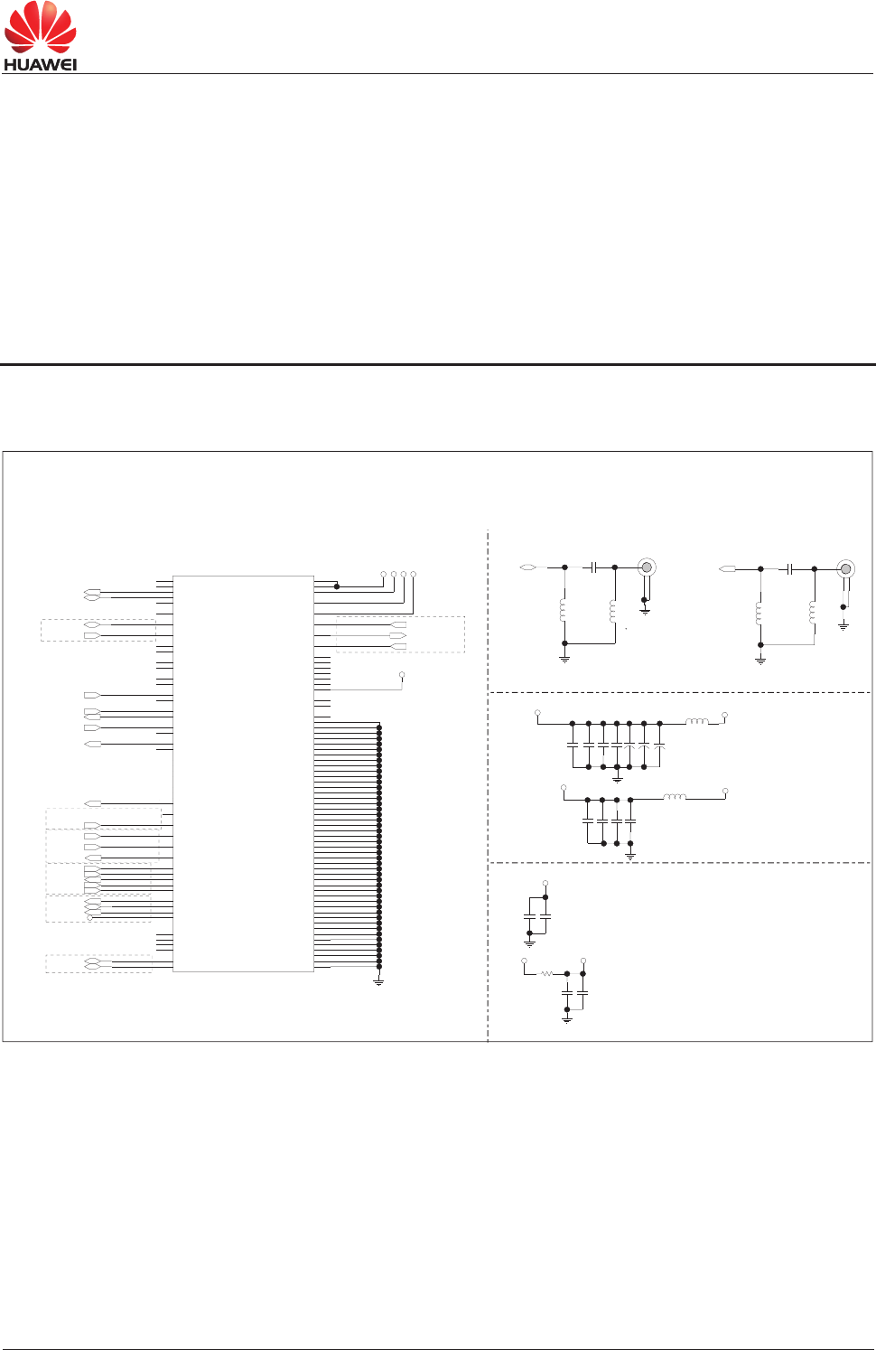
HUAWEI MU739 HSPA+ LGA Module
ecafretnI lacipyT fo tiucriC A xidneppA ediuG erawdraH
Issue 11 (2015-10-08) Huawei Proprietary and Confidential
Copyright © Huawei Technologies Co., Ltd.
77
9 Appendix A Circuit of Typical Interface
MU739
NC
MAIN_ANT
AUX_ANT
RESERVED
RESERVED
I2S_CLK0
I2S_RX
I2S_TX
I2S_WA0
LED
ON2_N
RESOUT_N
JTAG_TCK
JTAG_TDI
JTAG_TDO
JTAG_TMS
JTAG_TRST_N
SIM_CLK
SIM_IO
SIM_RST
SIM_VCC
NC
NC
NC
NC
USB_DM
USB_DP
VBAT_PA
VBAT_PA
VBAT_PMU
VCC_EXT1
VCC_IN
WAKEUP_IN
WAKEUP_OUT
W_DISABLE_N
NC1
NC2
NC3
NC4
NC
NC
USB_VBUS
RESERVED
RESERVED
NC
GND2
GND3
GND4
GND5
GND6
GND7
GND8
GND9
GND10
GND11
GND12
GND13
GND14
GND15
GND16
GND17
GND18
GND19
GND20
GND21
GND22
GND23
GND24
GND25
GND26
GND27
GND28
GND29
GND30
GND31
GND32
GND33
GND34
GND35
GND36
GND37
GND38
GND39
GND40
GND41
GND42
GND43
GND44
GND45
GND46
GND47
JTAG
LGA Module and ANT Interface
I2S
LED
USB
Control signal
NC
NC
NC
ON signal
USIM
Power suuply
RESET
should be connected to VBAT_PMU if use USB;
ANT
USB_VBUS is for USB
keep NC if don't need USB
These components values should be adjusted according to actual PCB layout and routings
SLEEP_STATUS
41
44
17
16
6
69
65
72
15
14
22
21
19
18
55
54
56
57
58
59
46
45
26
28
30
37
36
35
33
34
13
48
53
31
9
12
11
2
10
8
27
29
25
20
7
5
1
3
24
23
51
52
49
38
40
42
43
39
75
76
77
78
60
4
32
47
50
61
62
63
64
66
67
68
70
71
73
74
79
80
81
82
83
84
85
86
87
88
89
90
91
92
93
94
95
96
97
98
99
100
101
102
103
104
105
106
107
108
109
110
111
112
113
114
VCC_EXT1_1V8
VCC_IN
VBAT_PMU
USB_DP
I2S_TX
I2S_RX
I2S_CLK0
MAIN_ANT
USB_VBUS
WAKEUP_OUTAUX_ANT
AUX_ANT
MAIN_ANT
L206 27N
L205 27N
L204 27N
L203 27N
C213 100PF
C212 100PF
2 3
1
0
J202
1
3 2
J201
0
USB_DM
SIM_VCC
SIM_RST
SIM_DATA_0
SIM_CLK
JTAG_TRST_N
JTAG_TMS
JTAG_TDO
JTAG_TDI
JTAG_TCK
RESOUT_N
ON2_N
LED
I2S_WA0
VBAT_PA_DCDC
WAKEUP_IN
W_DISABLE_N
+
++
close to pin 49
close to pin 51/52
C204
22U
2 1
C217
220U
2 1
C218
220U
2 1
C219
220U
C216
22U
L201 -100
330P
C201
L202 -100
VBAT_PMU
VBAT
VBAT
100NF
C202
C207
1UF100NF
C206 C203
1UF
C205
330P
VBAT_PA_DCDC
close to pin 40
close to pin 38
VCC_EXT1_1V8 VCC_IN
R2010
4.7UF
C209
100NF
C208
4.7UF
C211
100NF
C210
VCC_EXT1_1V8
USIM_DET USIM_DET
S
LEEP_
STATUS
RESERVED
RESERVED
RESERVED
RESERVED
RESERVED
RESERVED
RESERVED
RESERVED
RESERVED
##
RESERVED
RESERVED
RESERVED
RESERVED
RESERVED
RESERVED
RESERVED
RESERVED
BODYSAR_N BODYSAR_N
RESET_BB_N
RESET_PMU_N
RESET_BB_N
RESET_PMU_N
RESERVED
U
U
U
U
U
U
U
U
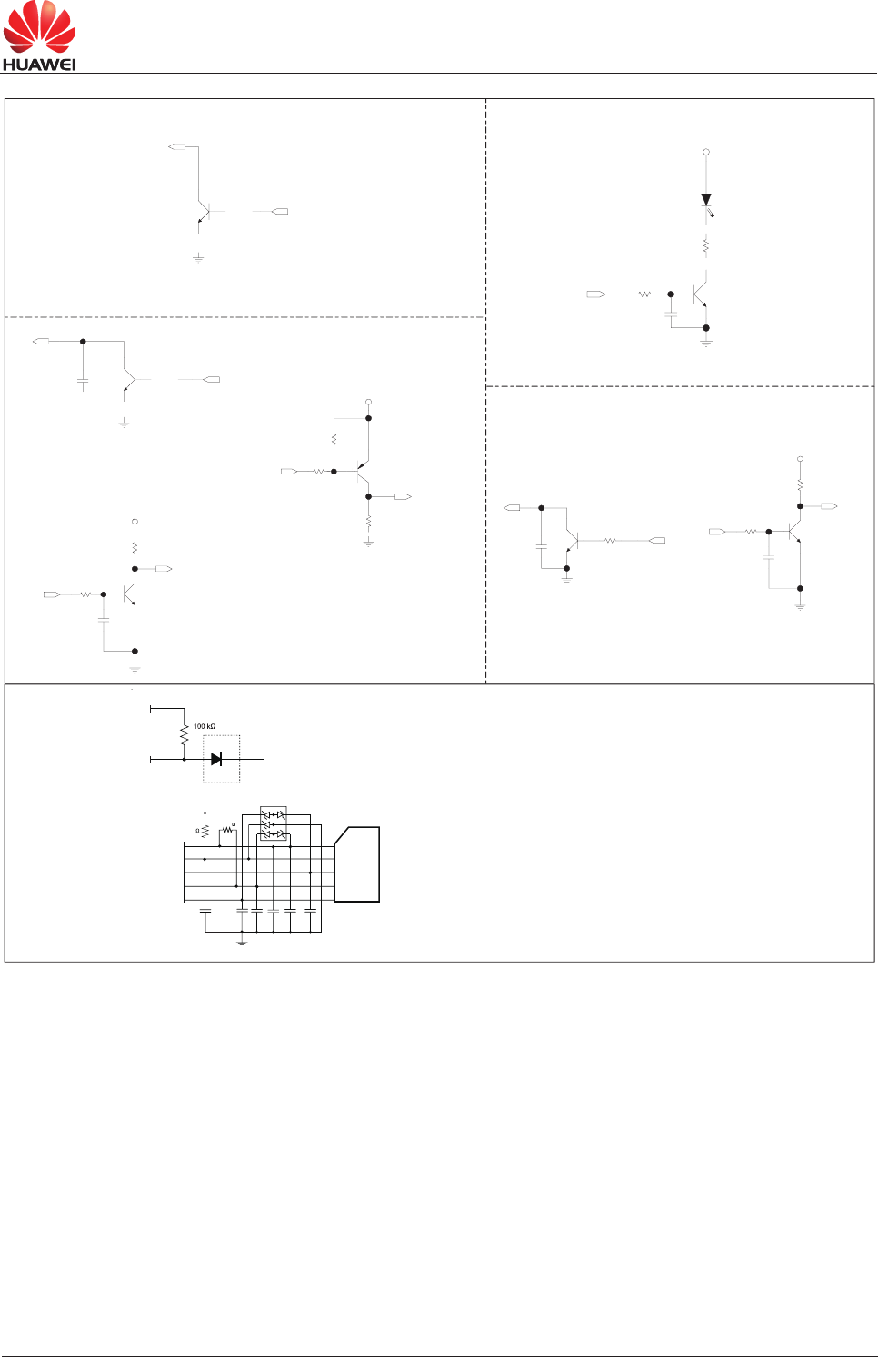
HUAWEI MU739 HSPA+ LGA Module
ecafretnI lacipyT fo tiucriC A xidneppA ediuG erawdraH
Issue 11 (2015-10-08) Huawei Proprietary and Confidential
Copyright © Huawei Technologies Co., Ltd. 78
LED
B
EC
B
C
E
NPN-BEC
B
CE
NPN-BEC
B
CE
NPN-BEC
B
C
E
NPN-BEC
power supply from AP
wakeup signal to AP
RESET_OUT would be monitored by a host processor GPIO (with internal PU)also.
ON2_N can be controlled by a host processor
GPIO(with internal PU under reset) also
power supply from AP
ON signal from AP
ON2_N: Low level active
RESET signal from AP
VIO_AP
VIO_AP
R3142.2K
RESOUT_N
LED#
RESOUT_N_AP
WAKEUP_OUT_N_AP
WAKEUP_OUT
RESET_BB_N
RESET_BB_N_AP
ON2_N
O2N_AP
VBAT_PMU
100NF C303
1
3
2
Q308
1
32
Q303
2.2K
1K
R311
1
32
Q301
100NF
C305
100K R312
1
3
2
Q306
R307 10K
R308 10K
1
23
Q304
C301
33PF
R316 200 2 1
D1
R301 2.2K
R306 2.2K
B
CE
NPN-BEC
W_DISABLE signal from AP
C306
33PF
1
32
Q309
R318 2.2K
W_DISABLE_N
W_DISABLE_AP
B
CE
NPN-BEC
power supply from AP
Sleep status to AP
23
1
Q320
C340100NF
R321100K
R320
2.2K
SLEEP_STATUS
SLEEP_STATUS_AP
VIO_AP
proximity sensor input
VCC_EXT1
BODYSAR_N
Diode
USIM
4.7 k
33 pF 33 pF 33 pF
33 pF
33 pF
ESD protection
SIM_VCC
SIM_CLK
SIM_DATA
SIM_RST
4.7 k
SIM_DET
1µF
U
U
U
U
U
VCC_EXT1
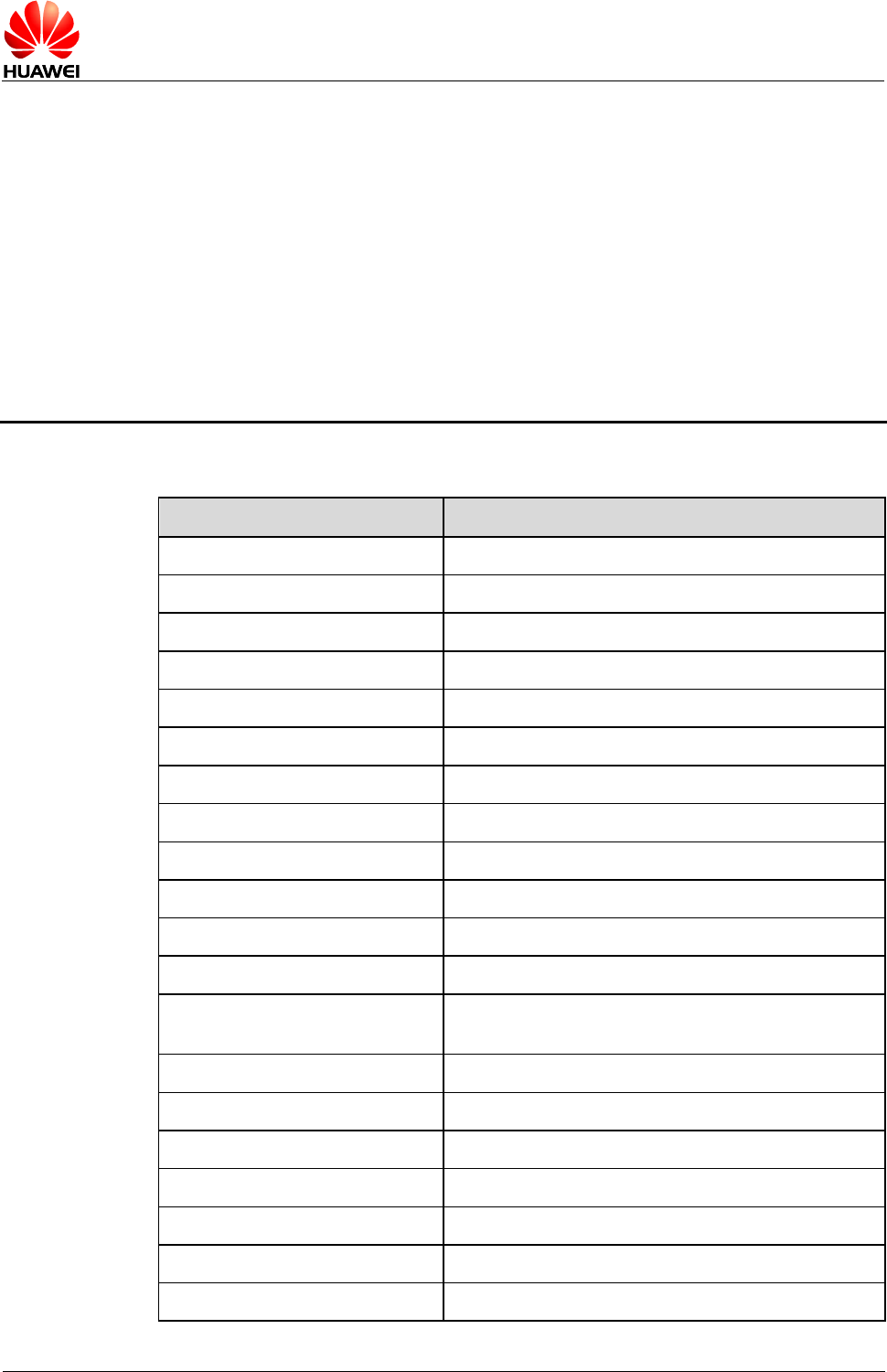
HUAWEI MU739 HSPA+ LGA Module
Hardware Guide
Appendix B Acronyms and Abbreviations
Issue 11 (2015-10-08)
Huawei Proprietary and Confidential
Copyright © Huawei Technologies Co., Ltd.
79
10 Appendix B Acronyms and
Abbreviations
Acronym or Abbreviation
Expansion
CCC
China Compulsory Certification
CE
European Conformity
CS
Coding Scheme
CSD
Circuit Switched Data
DC
Direct Current
DMA
Direct Memory Access
EBU
External Bus Unit
EIA
Electronic Industries Association
EMC
Electromagnetic Compatibility
ESD
Electrostatic Discharge
EU
European Union
FCC
Federal Communications Commission
FDD-TDMA
Frequency Division Duplexing–Time Division
Multiple Access
GMSK
Gaussian Minimum Shift Keying
GPIO
General-purpose I/O
GPRS
General Packet Radio Service
GSM
Global System for Mobile Communication
HSDPA
High Speed Downlink Packet Access
HSPA+
Enhanced High Speed Packet Access
HSUPA
High Speed Up-link Packet Access
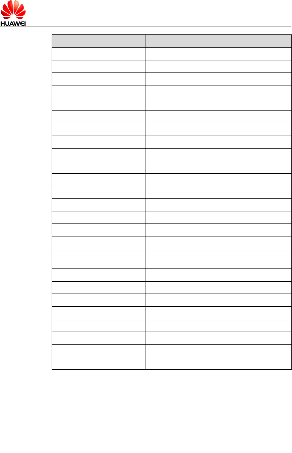
HUAWEI MU739 HSPA+ LGA Module
Hardware Guide
Appendix B Acronyms and Abbreviations
Issue 11 (2015-10-08)
Huawei Proprietary and Confidential
Copyright © Huawei Technologies Co., Ltd.
80
Acronym or Abbreviation
Expansion
IPC
Inter Processor Communications
ISO
International Standards Organization
I2S
I2C Sound
LCP
Liquid Crystal Polyester
LDO
Low-Dropout
LED
Light-Emitting Diode
LGA
Land Grid Array
MCP
Multi-chip Package
MIPI
Mobile Industry Processor Interface
NTC
Negative Temperature Coefficient
PA
Power Amplifier
PBCCH
Packet Broadcast Control Channel
PCB
Printed Circuit Board
PDU
Protocol Data Unit
PMU
Power Management Unit
RF
Radio Frequency
RoHS
Restriction of the Use of Certain Hazardous
Substances
RTC
Real-time Clock
TTL
Transistor-transistor Logic
TVS
Transient Voltage Suppressor
UMTS
Universal Mobile Telecommunications System
USB
Universal Serial Bus
USIM
Universal Subscriber Identity Module
VSWR
Voltage Standing Wave Ratio
WCDMA
Wideband Code Division Multiple Access
