HuiZhou BoShiJie Technology RC10 GSM wireless data module User Manual
HuiZhou BoShiJie Technology CO.,Ltd GSM wireless data module
User Manual
User Manual
HuiZhou BoShiJie Technology CO.,Ltd
Product name:GSM wireless data module
Model: RC10
FCC ID : 2AQSK- RC10

Overview
The RC10 module is a two-in-one module (2G wireless communication and
positioning) based on the MTK 2503D, Size:24 mm×15 mm×3.0 mm, Total 57PIN,
Suitable for GSM networks for global roaming. The RC10 module with a
Abundant interface and a powerful software support platform. With secondary
development software and hardware platform, it can support a variety of peripheral
devices to meet the user's business function needs.
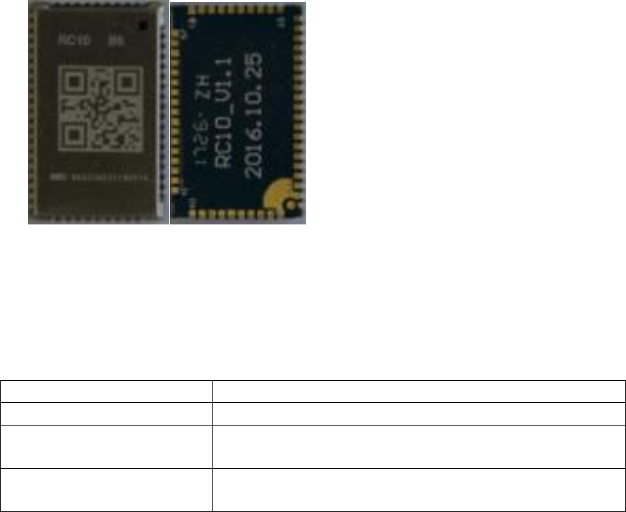
Ⅰ. The Appearance Of The Module
Ⅱ. Technical specifications
Main Technical Specifications Of The Rc10 Module
Product Feature
Description
Power Voltage
3.3V~4.6V(Recommended value4.0V)
Working Frequency
Quad-band: GSM850/EGSM900/DCS1800/PCS1900
Module can search for frequency bandsautomatically
GPRSData characteristics
GPRSData downlink transmission:maximum85.6Kbps
GPRSData uplink transmission:maximum42.8Kbps

Ⅲ. Pin definition
RC10 is an application mode with module as the main processor
1. Power supply
2. Serial Port
PIN Name
PIN No.
Description
Remark
UTXD1
23
Main Port:Print、
Download
Serial port power supply 2.8V
URXD1
22
GNSS_UART_T
X
46
GPS serial port
GNSS_UART_R
X
45
UTXD3
6
Serial port power supply2.8V
URXD3
7
3. SIM card port
PIN Name
PIN No.
Description
Remark
SIM1_SCLK
54
SIM card clock pin
SIM1_SRST
52
SIM card reset pin
SIM1_SIO
51
SIM card data pin
VSIM1
53
SIM card power-up pin
Power-up 1.8V or 3V
4. Booting
PIN Name
PIN No.
Description
Remark
PWRKEY
34
Module boot pin
Lower boot
5. Audio interface
PIN Name
PIN No.
Description
Remark
MIC_N0
44
Audio input
PIN Name
PIN No.
Description
Remark
VBAT
37、38
Power supply
Vmax=4.6V
Vmin=3.3V
Vnorm=4V
VBAT1
11
GPS power supply
Connect with 37
&38
VIO28
19
Output 2.8V
Max current 100mA
VRTC
47
RTC clock output
2.8V/2mA
GPS_RTC
15
GPS clock input
GND
1、29、31、
36、48、55、
57
AGND

MIC_P0
43
SPKP1
42
Audio output
SPKN1
41
6. AD port
PIN Name
PIN No.
Description
Remark
AD0
40
AD detect
Max voltage 2.8V
AD1
39
AD detect
Max voltage 2.8V
7. Antenna
PIN Name
PIN No.
Description
Remark
ANT1
30
GSM Antenna
ANT2
56
GPS Antenna
8. USB download
PIN Name
PIN No.
Description
Remark
VBUS
35
Voltage 5V
Download detect
USB_DM
50
USB_DP
49
9. I2C port
PIN Name
PIN No.
Description
Remark
SCL
16
I2C clock pin
Voltage 2.8V
SDA
17
I2C data pin
Voltage 2.8V
10. GPIO port
PIN Name
PIN No.
Description
Remark
GPIO_0
21
Max Voltage 2.8V
GPIO_1
18
Max Voltage 2.8V
GPIO_2
13
Max Voltage 2.8V
GPIO_3
14
Max Voltage 2.8V
GPIO_4
9
Max Voltage 2.8V
GPIO_5
8
Max Voltage 2.8V
GPIO_6
5
Max Voltage 2.8V
GPIO_7
10
Max Voltage 2.8V
GPIO_8
12
Max Voltage 2.8V
GPIO_10
26
Max Voltage 2.8V
GPIO_11
25
Max Voltage 2.8V
GPIO_12
20
Max Voltage 2.8V
11. Others
PIN Name
PIN No.
Description
Remark

KCOL0
24
USB mode select
NC
2、3、4、27、
28、32、33
Hanging
IV. Attentions
1、Working voltage:3.3V~4.6V,typical voltage4.0V
2、Working current:Max working current 3A
3、Standby power consumption:18mA
4、Working temperature:-20°~80°
5、Module size:24*15mm
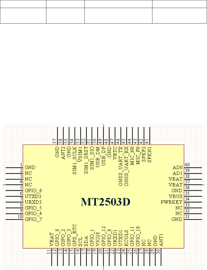
V. Schematic diagramencapsulate
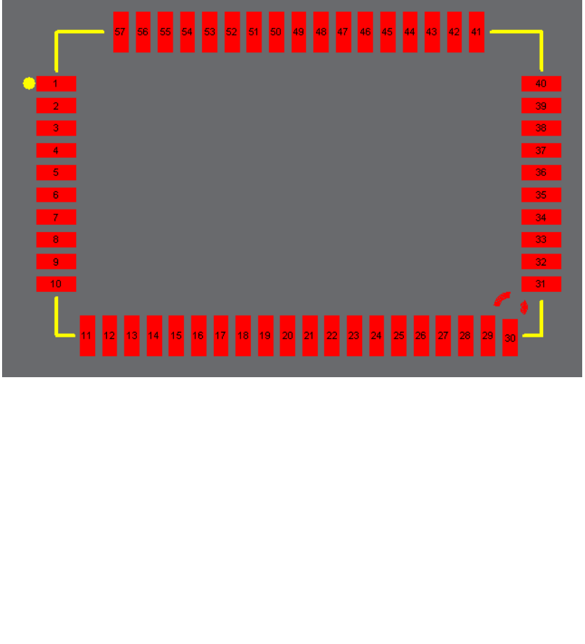
VI. PCB encapsulate

Installation warning statement
(a)product should not collocate with other radio
(b) GSM wireless data module is designed to comply with the ID statement. FCC ID is
2AQSK- RC10. The host system using GSM wireless data module, should have label
indicated FCC ID 2AQSK- RC10
(c) If you buy this module,you only use the the antenna(The Gain is 1.80dBi for GSM850
and The antenna is 2.50dBi for GSM1900) of GSM wireless data module,Do not use the
other antenna
(d): The GSM wireless data module is Only applicable for the mobile device.
FCC Statement
This device complies with part 15 of the FCC Rules. Operation is subject to the following
two conditions:
(1) This device may not cause harmful interference, and (2) this device must accept any
interference received, including interference that may cause undesired operation.
Any Changes or modifications not expressly approved by the party responsible for
compliance could void the user’s authority to operate the equipment.
Note: This equipment has been tested and found to comply with the limits for a Class B
digital device, pursuant to part 15 of the FCC Rules. These limits are designed to provide
reasonable protection against harmful interference in a residential installation. This
equipment generates uses and can radiate radio frequency energy and, if not installed
and used in accordance with the instructions, may cause harmful interference to radio
communications. However, there is no guarantee that interference will not occur in a
particular installation. If this equipment does cause harmful interference to radio or
television reception, equipment generates, uses and can radiate radio frequency energy
and, if not installed and used in accordance with the instructions, may cause harmful
interference to radio communications. However, there is no guarantee that interference
will not occur in a particular installation. If this equipment does cause harmful interference
to radio or television reception,
—Reorient or relocate the receiving antenna.
—Increase the separation between the equipment and receiver.
—Connect the equipment into an outlet on a circuit different from that to which the
receiver is connected.
—Consult the dealer or an experienced radio/TV technician for help.
FCC RF Radiation Exposure Statement
This equipment complies with FCC RF radiation exposure limits set forth for an
uncontrolled environment. This equipment should be installed and operated with a
minimum distance of 20 centimeters between the radiator and your body. for example Used
in Such as Car locator, etc.