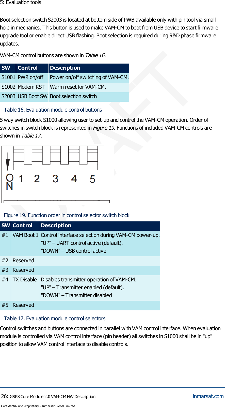
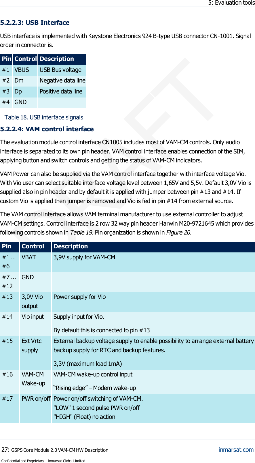
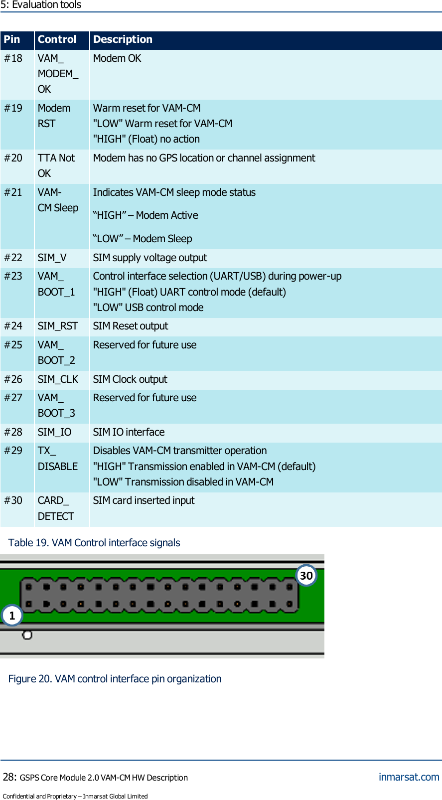
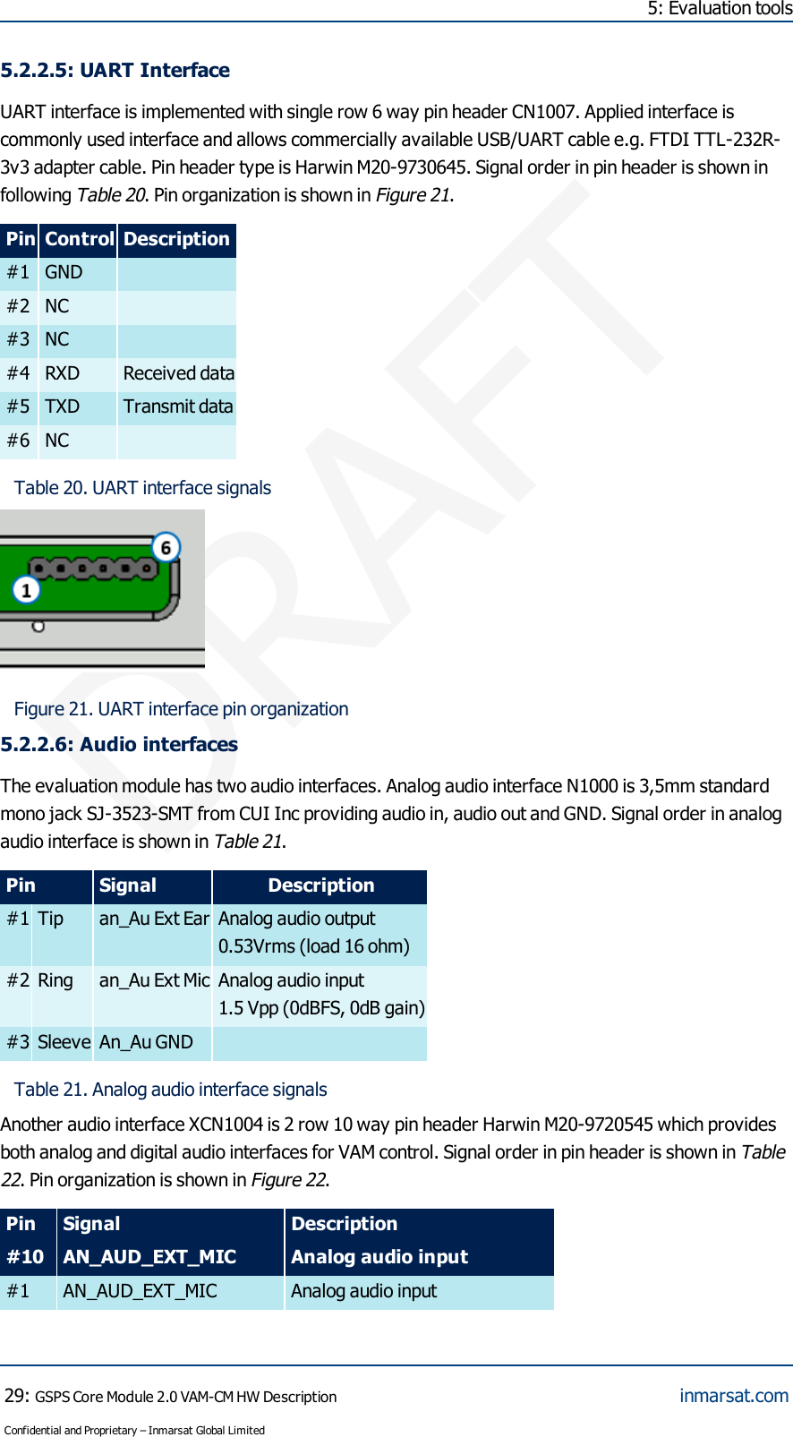
Inmarsat GSPSCM2 Satellite Radio Module for Inmarsat GMR2+ network User Manual My
Inmarsat Limited Satellite Radio Module for Inmarsat GMR2+ network My
UserManual.wiki
>
Inmarsat
>
GSPSCM2 User Manual
>
User manual
Contents
1.
User manual
2.
User manual supplement
3.
antenna installation
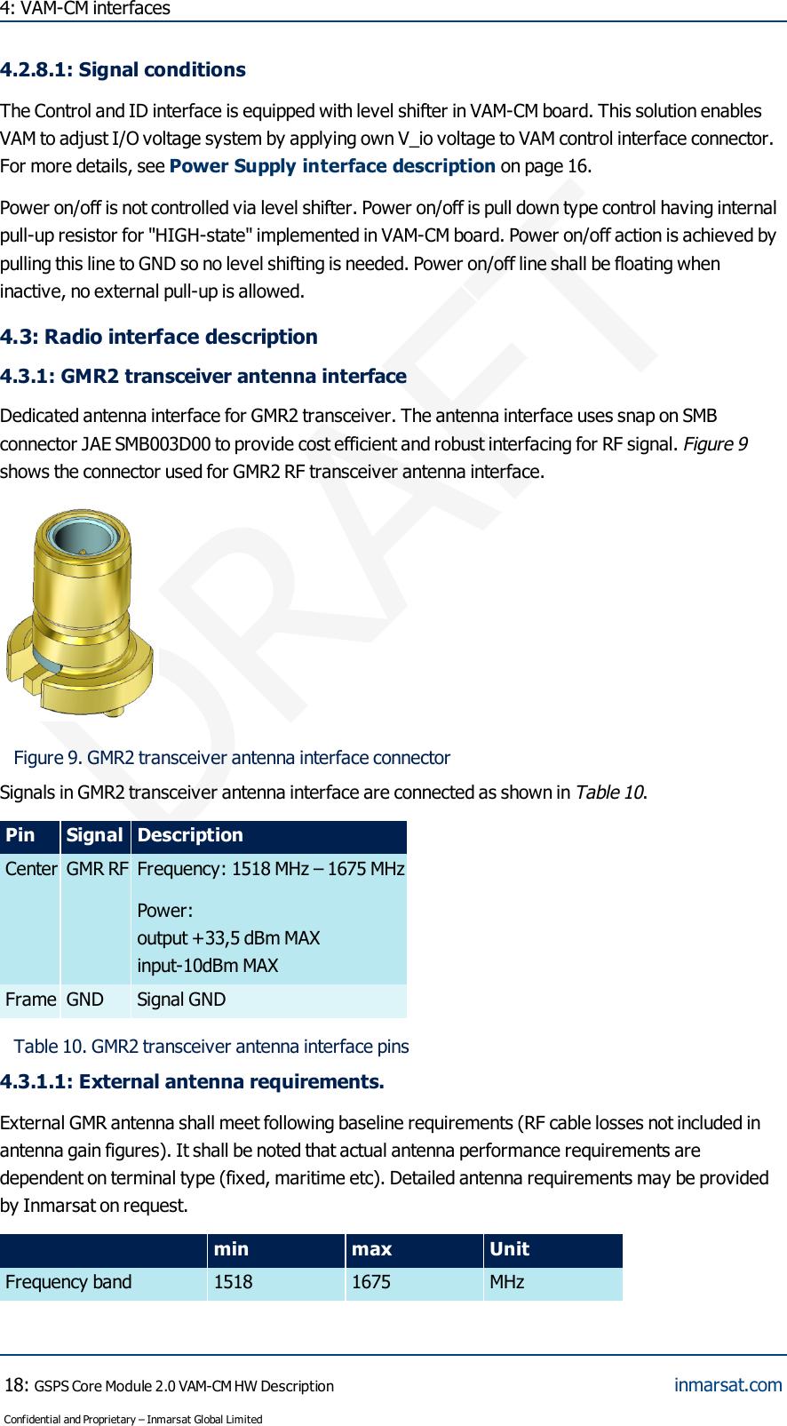
4.
Antenna sales sheet
5.
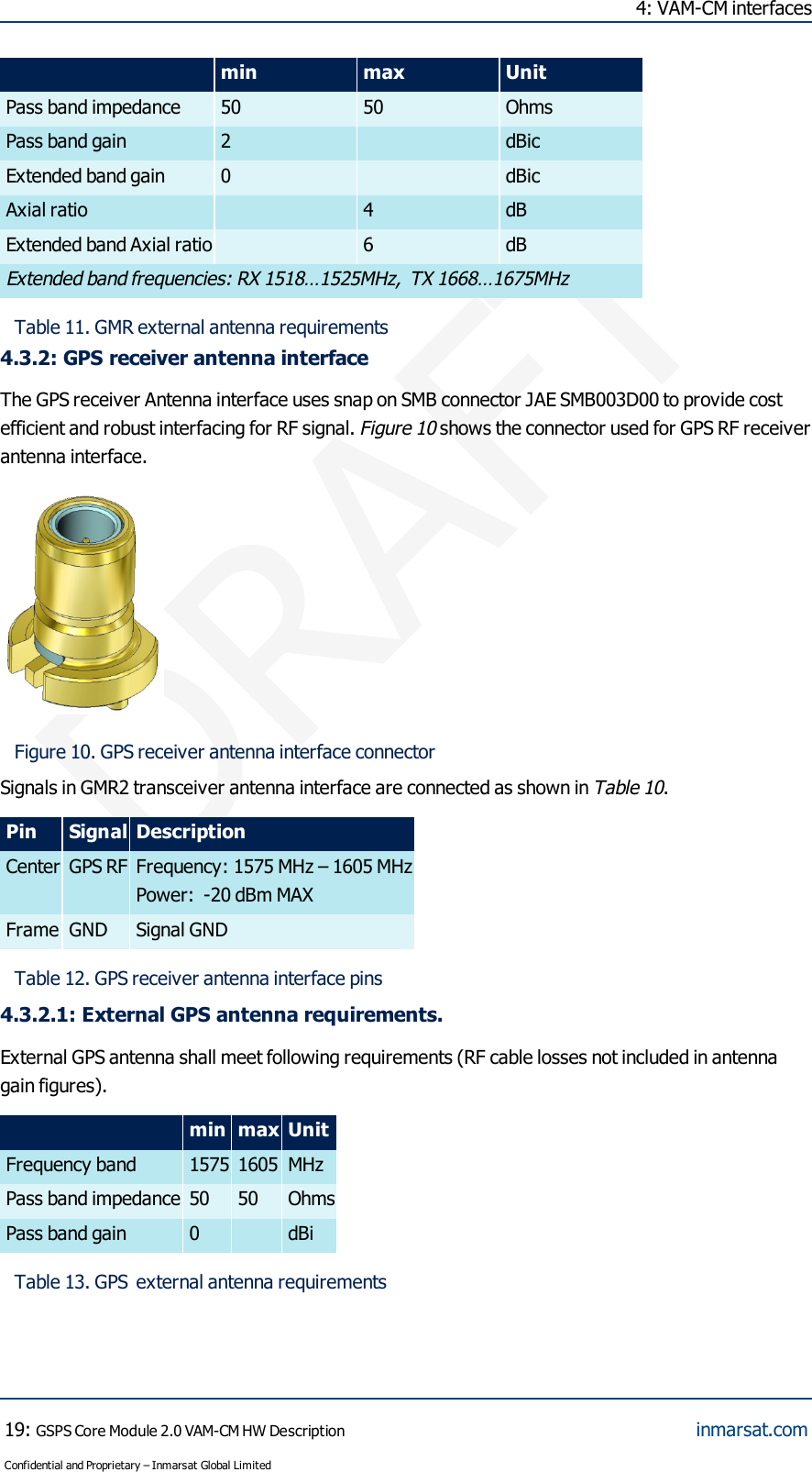
Antenna installation
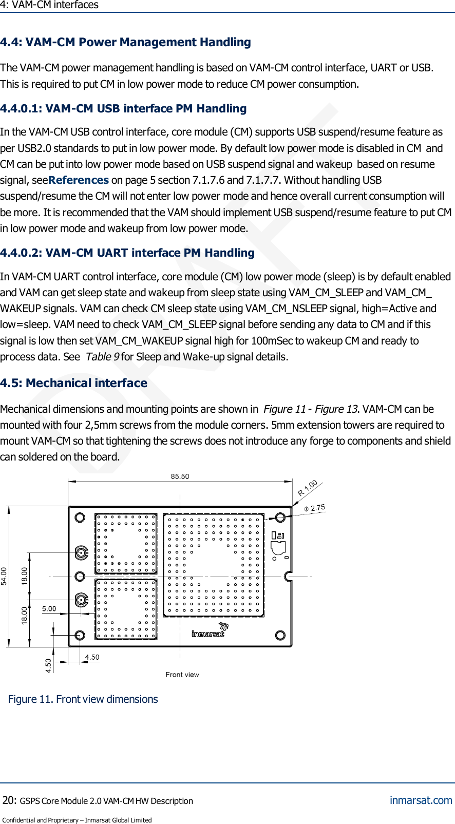
User manual
Navigation menu
Upload a User Manual
Namespaces
Wiki Guide
HTML
PDF
Info
Views
User Manual
Discussion / Help
Navigation
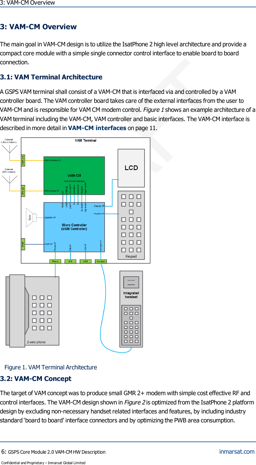
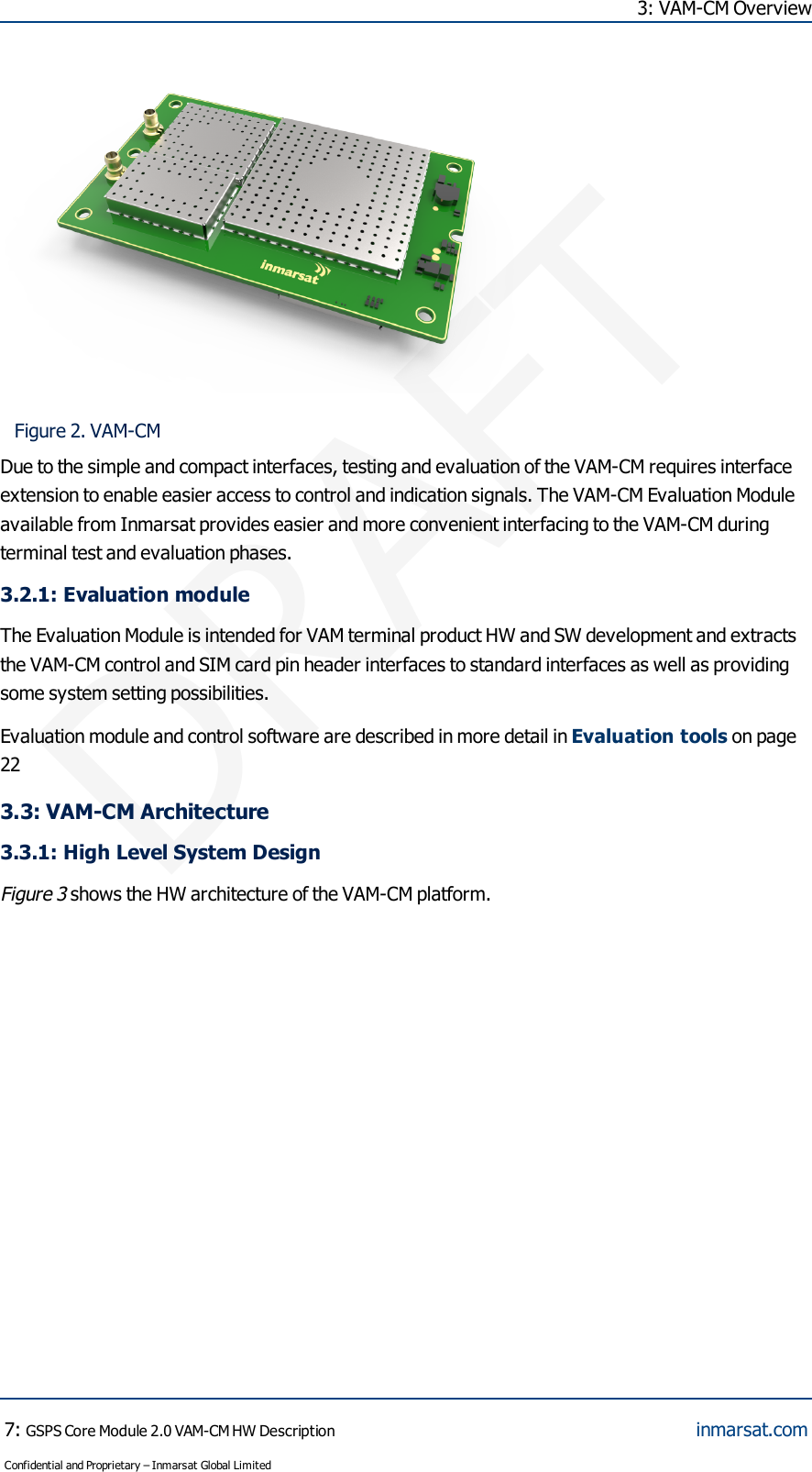
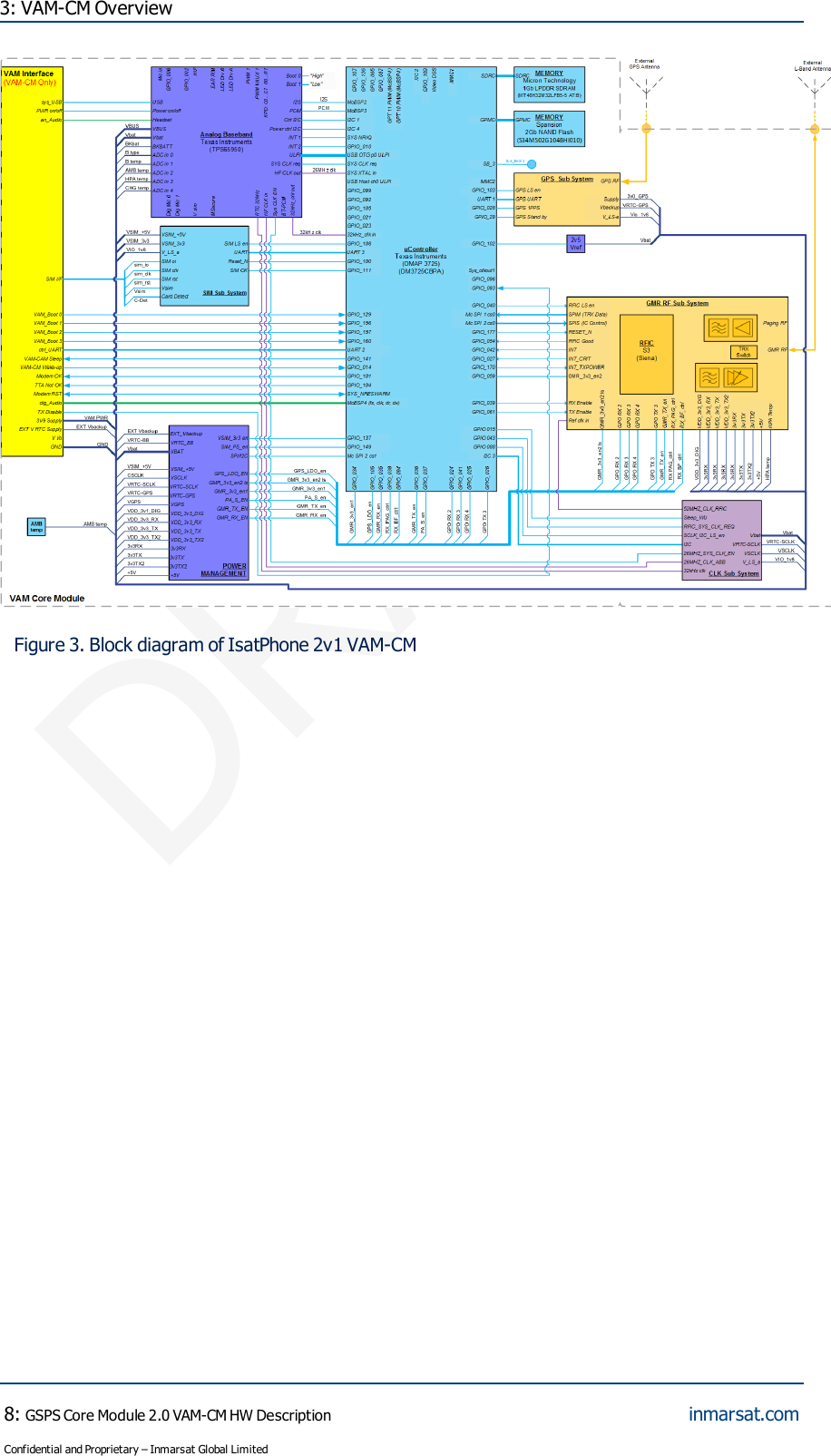
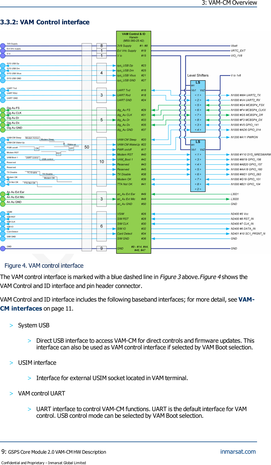
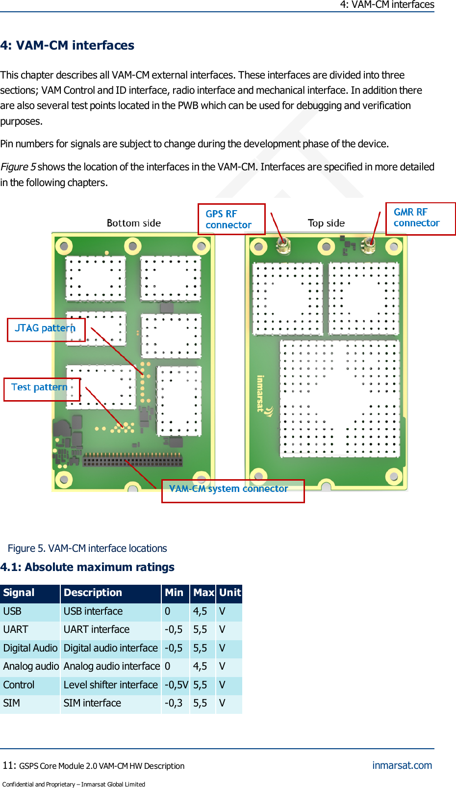
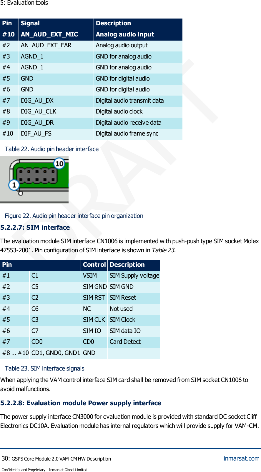
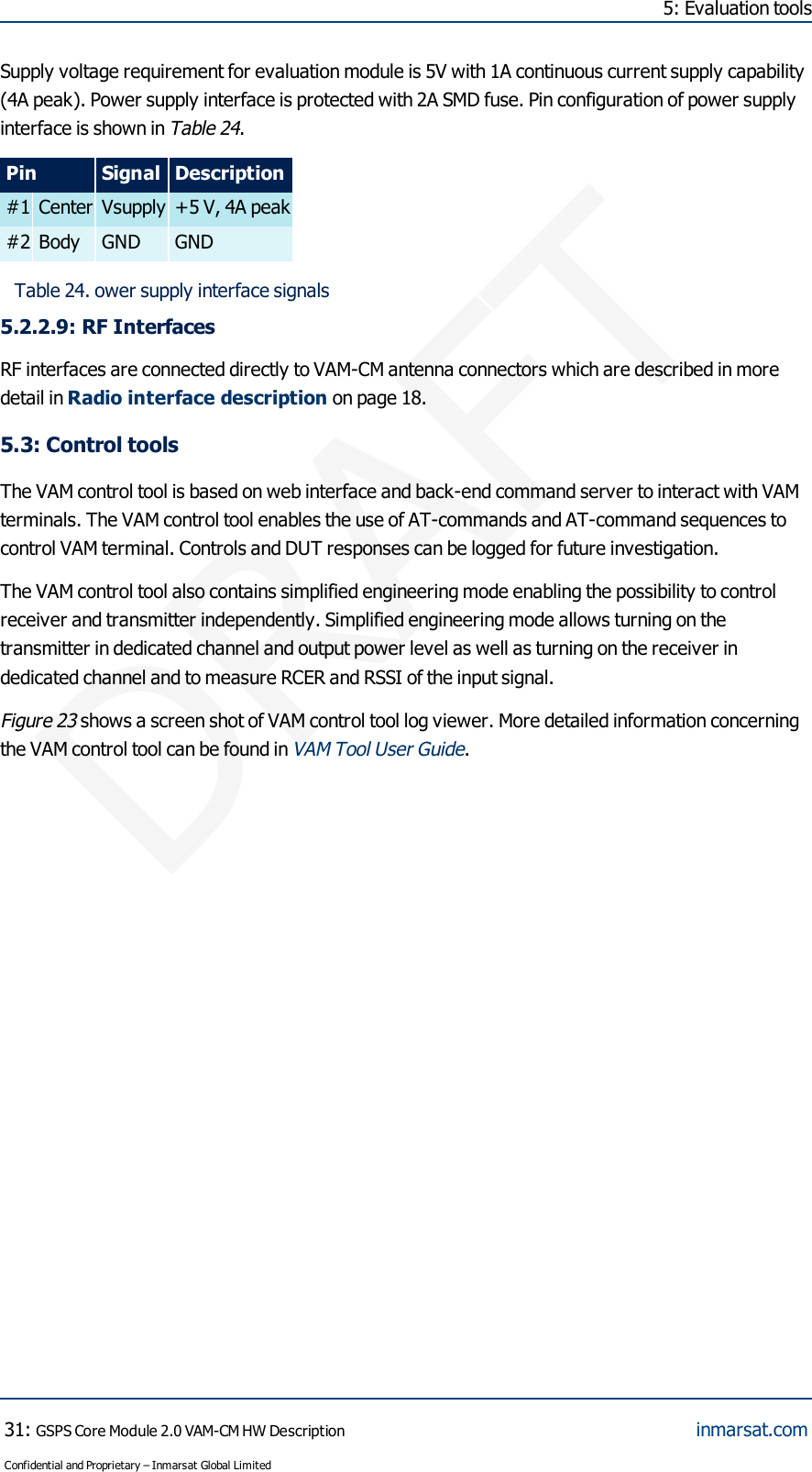
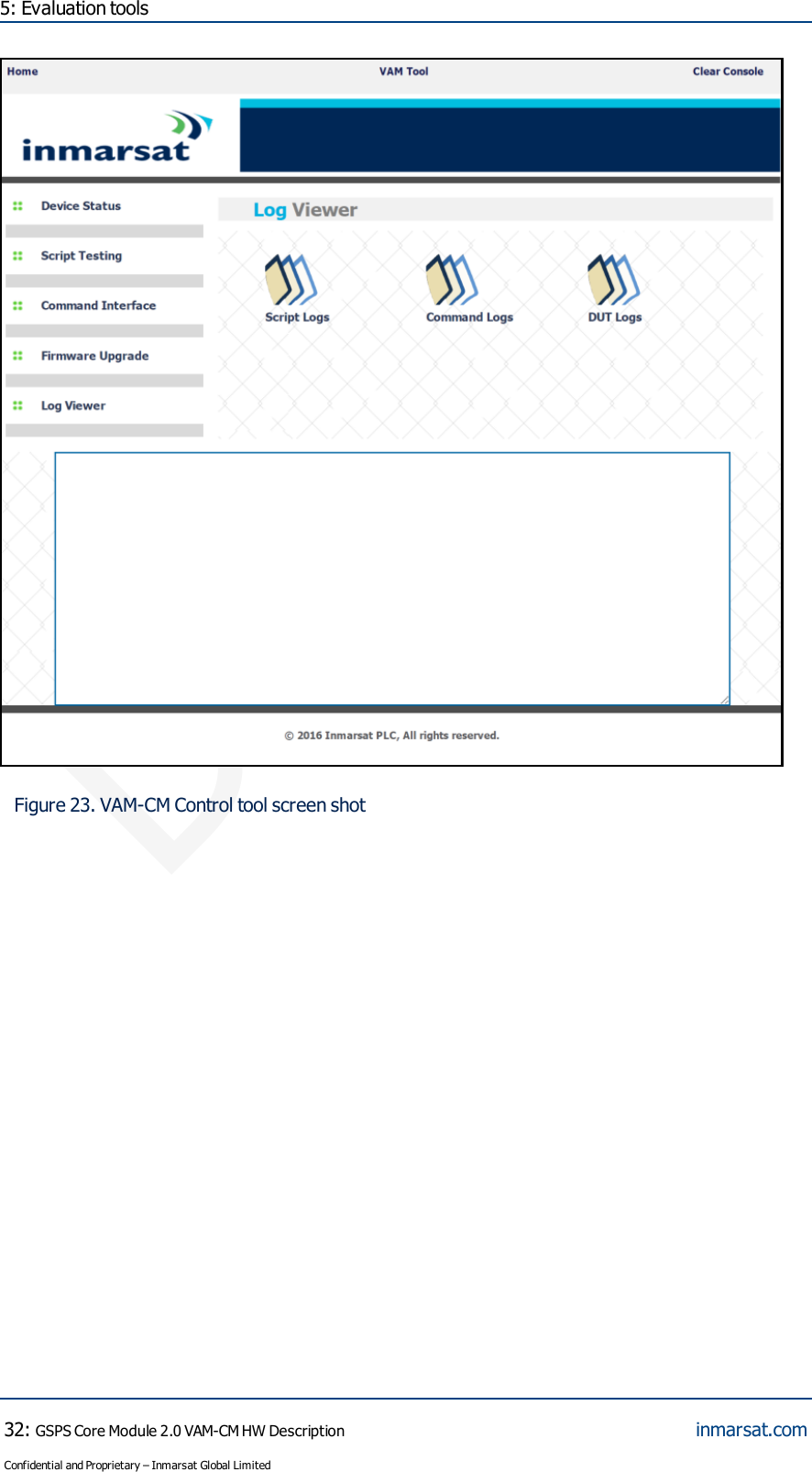
![DRAFT2: Scope2: ScopeThis document describes the HW Interfaces of VAM-Core Module (VAM-CM). Interfaces of VAM-CMare dedicated for VAM manufacturers to interface their own satellite terminal UI and controlelectronics.The intended audiences are engineers from Inmarsat, LM, manufacturing partners, VAMmanufacturers and Sasken and a working knowledge of the Inmarsat space segment and GMR2+specification is assumed.2.1: ReferencesReference Document Version[R1]VAM Tool User Guide1.0[R2]Standard and Proprietary ATCommands1.0-1[R3]VAM Core Module User Guide0.95:GSPS Core Module 2.0 VAM-CM HW DescriptionConfidential and Proprietary – Inmarsat Global Limitedinmarsat.com](https://usermanual.wiki/Inmarsat/GSPSCM2.User-manual/User-Guide-3495911-Page-5.png)