Inmarsat GSPSCM2 Satellite Radio Module for Inmarsat GMR2+ network User Manual My
Inmarsat Limited Satellite Radio Module for Inmarsat GMR2+ network My
Inmarsat >
Contents
User manual

DRAFT
While the information in this document has been prepared in good faith, no representation, warranty, assurance or undertaking (express or implied) is or will be made, and no responsibility or liability (howsoever arising)
is or will be accepted by the Inmarsat group or any of its officers, employees or agents in relation to the adequacy, accuracy, completeness, reasonableness or fitness for purpose of the information in this document. All
and any such responsibility and liability is expressly disclaimed and excluded to the maximum extent permitted by applicable law. INMARSAT is a trademark owned by the International Mobile Satellite Organisation, the
Inmarsat LOGO is a trademark owned by Inmarsat (IP) Company Limited. Both trademarks are licensed to Inmarsat Global Limited. All other Inmarsat trade marks in this document are owned by Inmarsat Global
Limited.
Confidential and Proprietary © Inmarsat Global Limited 2017. All rights reserved.
GSPS Core Module 2.0 VAM-CM HW
Description
Version 0.9
Publication Date: 13-Jan-2017
INMARSAT> GSPS

DRAFT
Contents
1: Purpose 4
2: Scope 5
2.1: References 5
3: VAM-CM Overview 6
3.1: VAM Terminal Architecture 6
3.2: VAM-CM Concept 6
3.2.1:Evaluation module 7
3.3: VAM-CM Architecture 7
3.3.1:High Level System Design 7
3.3.2:VAM Control interface 9
4: VAM-CM interfaces 11
4.1: Absolute maximum ratings 11
4.2: VAM Control interface description 12
4.2.1:System USB description 12
4.2.2:USIM interface description 13
4.2.3:VAM control UART interface description 13
4.2.3.1:Voltage levels 14
4.2.3.2:Interface control 14
4.2.3.3:Data formats 14
4.2.4:Analog Audio interface description 14
4.2.5:Digital Audio interface description 14
4.2.5.1:Voltage levels 15
4.2.5.2:Data formats 15
4.2.6:Power Supply interface description 16
4.2.7:External VRTCSupply Functionality 16
4.2.8:Control and ID interface description 17
4.2.8.1:Signal conditions 18
4.3: Radio interface description 18
2:GSPS Core Module 2.0 VAM-CM HW Description
Confidential and Proprietary – Inmarsat Global Limited
inmarsat.com

DRAFT
4.3.1:GMR2 transceiver antenna interface 18
4.3.1.1:External antenna requirements. 18
4.3.2:GPS receiver antenna interface 19
4.3.2.1:External GPS antenna requirements. 19
4.4: VAM-CM Power Management Handling 20
4.4.0.1:VAM-CM USB interface PM Handling 20
4.4.0.2:VAM-CM UART interface PM Handling 20
4.5: Mechanical interface 20
4.6: Environmental conditions 21
5: Evaluation tools 22
5.1: Evaluation kit 22
5.2: Evaluation module 22
5.2.1:Evaluation module size 23
5.2.2:Evaluation module interfaces 24
5.2.2.1:Indicators 25
5.2.2.2:Buttons and switches 25
5.2.2.3:USB Interface 27
5.2.2.4:VAM control interface 27
5.2.2.5:UART Interface 29
5.2.2.6:Audio interfaces 29
5.2.2.7:SIM interface 30
5.2.2.8:Evaluation module Power supply interface 30
5.2.2.9:RF Interfaces 31
5.3: Control tools 31
3:GSPS Core Module 2.0 VAM-CM HW Description
Confidential and Proprietary – Inmarsat Global Limited
inmarsat.com


DRAFT
2: Scope
2: Scope
This document describes the HW Interfaces of VAM-Core Module (VAM-CM). Interfaces of VAM-CM
are dedicated for VAM manufacturers to interface their own satellite terminal UI and control
electronics.
The intended audiences are engineers from Inmarsat, LM, manufacturing partners, VAM
manufacturers and Sasken and a working knowledge of the Inmarsat space segment and GMR2+
specification is assumed.
2.1: References
Reference Document Version
[R1]
VAM Tool User Guide
1.0
[R2]
Standard and Proprietary AT
Commands
1.0-1
[R3]
VAM Core Module User Guide
0.9
5:GSPS Core Module 2.0 VAM-CM HW Description
Confidential and Proprietary – Inmarsat Global Limited
inmarsat.com
DRAFT
3: VAM-CM Overview
3: VAM-CM Overview
The main goal in VAM-CM design is to utilize the IsatPhone 2 high level architecture and provide a
compact core module with a simple single connector control interface to enable board to board
connection.
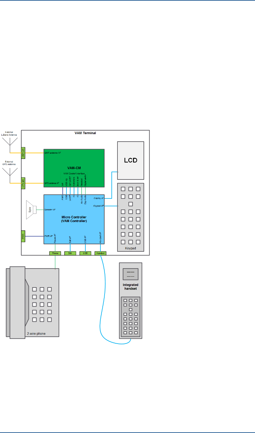
3.1: VAM Terminal Architecture
A GSPS VAM terminal shall consist of a VAM-CM that is interfaced via and controlled by a VAM
controller board. The VAM controller board takes care of the external interfaces from the user to
VAM-CM and is responsible for VAM CM modem control.
Figure 1
shows an example architecture of a
VAM terminal including the VAM-CM, VAM controller and basic interfaces. The VAM-CM interface is
described in more detail in VAM-CM interfaces on page 11.
Figure 1. VAM Terminal Architecture
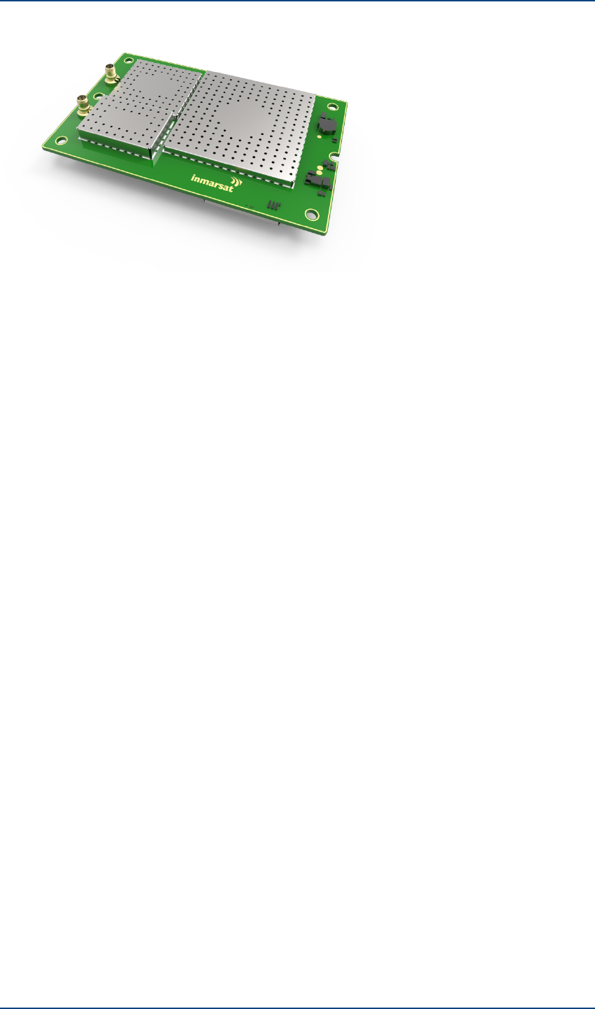
3.2: VAM-CM Concept
The target of VAM concept was to produce small GMR 2+ modem with simple cost effective RF and
control interfaces. The VAM-CM design shown in
Figure 2
is optimized from the IsatPhone 2 platform
design by excluding non-necessary handset related interfaces and features, by including industry
standard ‘board to board’ interface connectors and by optimizing the PWB area consumption.
6:GSPS Core Module 2.0 VAM-CM HW Description
Confidential and Proprietary – Inmarsat Global Limited
inmarsat.com
DRAFT
3: VAM-CM Overview
Figure 2. VAM-CM
Due to the simple and compact interfaces, testing and evaluation of the VAM-CM requires interface
extension to enable easier access to control and indication signals. The VAM-CM Evaluation Module
available from Inmarsat provides easier and more convenient interfacing to the VAM-CM during
terminal test and evaluation phases.
3.2.1:Evaluation module
The Evaluation Module is intended for VAM terminal product HW and SW development and extracts
the VAM-CM control and SIM card pin header interfaces to standard interfaces as well as providing
some system setting possibilities.
Evaluation module and control software are described in more detail in Evaluation tools on page
22
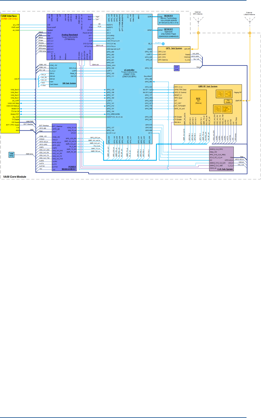
3.3: VAM-CM Architecture
3.3.1:High Level System Design
Figure 3
shows the HW architecture of the VAM-CM platform.
7:GSPS Core Module 2.0 VAM-CM HW Description
Confidential and Proprietary – Inmarsat Global Limited
inmarsat.com
DRAFT
3: VAM-CM Overview
3.3.2:VAM Control interface
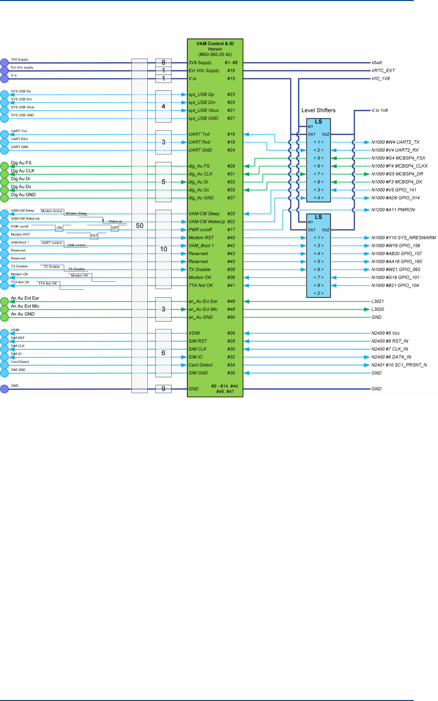
Figure 4. VAM control interface
The VAM control interface is marked with a blue dashed line in
Figure 3
above.
Figure 4
shows the
VAM Control and ID interface and pin header connector.
VAM Control and ID interface includes the following baseband interfaces; for more detail, see VAM-
CM interfaces on page 11.
>System USB
>Direct USB interface to access VAM-CM for direct controls and firmware updates. This
interface can also be used as VAM control interface if selected by VAM Boot selection.
>USIM interface
>Interface for external USIM socket located in VAM terminal.
>VAM control UART
>UART interface to control VAM-CM functions. UART is the default interface for VAM
control. USB control mode can be selected by VAM Boot selection.
9:GSPS Core Module 2.0 VAM-CM HW Description
Confidential and Proprietary – Inmarsat Global Limited
inmarsat.com

DRAFT
3: VAM-CM Overview
>Analog Audio interface
>Analog audio in (Ext Mic) and audio out (Ex Ear) signals.
>Digital Audio interface
>Digital PCM audio interface
>Power Supply interface
>Power supply for VAM-CM
>Control and ID interface
>Digital operating mode controls
>This interface includes VAM CM boot mode pins to initialize VAM CM in correct
operating mode. (Control interface, audio interface, modem reset etc.)
>This interface also includes some informative data from VAM CM. (Modem Good, TTA
Not OK, etc,)
10:GSPS Core Module 2.0 VAM-CM HW Description
Confidential and Proprietary – Inmarsat Global Limited
inmarsat.com
DRAFT
4: VAM-CM interfaces
4: VAM-CM interfaces
This chapter describes all VAM-CM external interfaces. These interfaces are divided into three
sections; VAM Control and ID interface, radio interface and mechanical interface. In addition there
are also several test points located in the PWB which can be used for debugging and verification
purposes.
Pin numbers for signals are subject to change during the development phase of the device.
Figure 5
shows the location of the interfaces in the VAM-CM. Interfaces are specified in more detailed
in the following chapters.
Figure 5. VAM-CM interface locations
4.1: Absolute maximum ratings
Signal Description Min Max Unit
USB USB interface 0 4,5 V
UART UART interface -0,5 5,5 V
Digital Audio Digital audio interface -0,5 5,5 V
Analog audio Analog audio interface 0 4,5 V
Control Level shifter interface -0,5V 5,5 V
SIM SIM interface -0,3 5,5 V
11:GSPS Core Module 2.0 VAM-CM HW Description
Confidential and Proprietary – Inmarsat Global Limited
inmarsat.com
DRAFT
4: VAM-CM interfaces
Signal Description Min Max Unit
PWR on/off Power on/off control 0 4,5 V
Supply Supply voltage 2,1 4,5 V
Vio IO system voltage -0,5 5,5 V
Table 1. Absolute maximum ratings
4.2: VAM Control interface description
The VAM control interface is a combination of digital and analog baseband interfaces dedicated to
control the VAM-CM. The Interface also includes other user interface related signals like USIM and
audio. The VAM control interface is a Harwin M50-360-25 42 male type pin header connector. The
Connector is located so trace lengths are short enough to enable correct functionality of all
interfaces.
The VAM-CM processor (DM3725) uses 1,8V I/O system. In order to protect the processor, digital
interfaces are connected via level shifters. A VAM terminal can determine the interface voltage level
by applying the desired V_io voltage to the VAM control interface connector. Voltage requirements
for logic levels are shown in
Table 2
. For more details, see Power Supply interface description
on page 16.
Description Min Max Unit
VIH High level input voltage VIO – 0,4 VIO V
VIL Low level input voltage 0 0,15 V
VOH High level output voltage VIO * 0,67 VIO V
VOL Low level output voltage VIO <3V 0 0,4 V
VIO >=3V 0,55 V
Table 2. Logic levels for Level Shifter
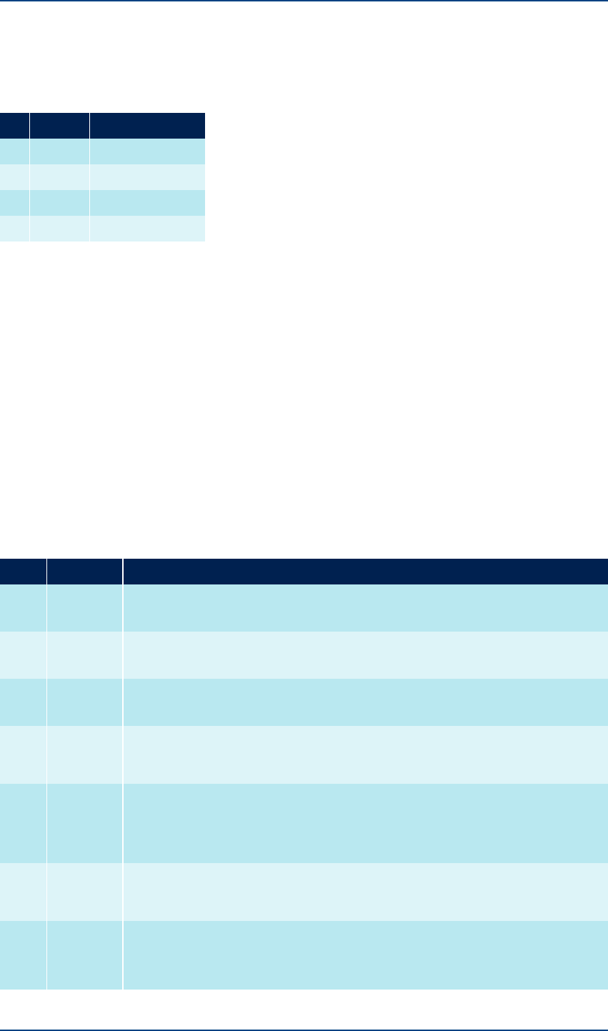
Figure 6. VAM-Control interface connector
Figure 6
shows the connector used for VAM control interface and pin arrangement. Following
chapters describe the sub interfaces and their location in connectors.
4.2.1:System USB description
The system USB interface is a dedicated interface providing access to the VAM-CM. This interface is
targeted for firmware updates and direct VAM-CM controls. The system USB connector shall be
routed out from VAM terminal for direct access. The system USB interface can also be used for VAM-
CM control when USB mode is selected with VAM Boot selector during VAM-CM power-on. The VAM
can put CM in low power mode by sending USB suspend command and wakeup is initiated by
sending resume command. Refer to VAM-CM USB interface PM Handling on page 20 for CM
low power (Sleep state) handling.
System USB interface signals are located in VAM Control interface as described in
Table 3
.
12:GSPS Core Module 2.0 VAM-CM HW Description
Confidential and Proprietary – Inmarsat Global Limited
inmarsat.com
DRAFT
4: VAM-CM interfaces
Pin Signal Description
#21 VBUS Supply voltage, 5,5V max
#23 Dp Digital data
#25 Dm Digital data
#27 GND Signal GND
Table 3. System USB interface pins
4.2.2:USIM interface description
The USIM interface provides USIM interface from the VAM-CM to VAM terminal for easier user
access.
The USIM reader in VAM terminal should be placed so that trace length from VAM control interface to
USIM reader shall not exceed 300mm.
USIM interface signals are located in VAM Control interface as described in
Table 4
.
Pin Signal In/out Description
#26 SIM_V Out Supply voltage for SIM.
#28 SIM_RST Out Digital data
#30 SIM_CLK Out Digital clock
#32 SIM_IO In/Out Digital data
#34 Card detect In "HIGH" (Float) = Card not present
"LOW" = Card present
#36 SIM_GND Signal GND
Table 4. USIM interface pins
4.2.3:VAM control UART interface description
The VAM control UART interface provides for VAM terminal to control VAM-CM features. The UART
interface is connected via level shifter circuit which allows VAM terminal to determine the signal
voltage level using V_io pin in VAM-CM system connector.
The UART control interface is the default control interface for VAM-CM. The Control interface can be
changed to USB using VAM Boot selector (
Table 9
).
VAM control UART interface signals are located in VAM Control interface as described in
Table 5
.
VAM-CM is using 2-wire UART interface with TXD, RXD signals. VAM_CM_WAKEUP and VAM_CM_
SLEEP signals is used to wake up CM from sleep state (low power mode) and to get CM sleep state
status, refer VAM-CM UART interface PM Handling on page 20 section for CM low power
(Sleep state) handling
Pin Signal In/Out Description
#16 TXD Out UART transmit data
#18 RXD In UART receive data
#24 GND UART GND
Table 5. VAM control UART interface pins
13:GSPS Core Module 2.0 VAM-CM HW Description
Confidential and Proprietary – Inmarsat Global Limited
inmarsat.com
DRAFT
4: VAM-CM interfaces
4.2.3.1:Voltage levels
The UART control bus is equipped with level shifter in VAM-CM board. This solution enables VAM to
adjust I/O voltage system by applying own V_io voltage to VAM control interface connector. Voltage
requirements for logic levels are shown in
Table 2
. More details in chapter Power Supply
interface description on page 16.
4.2.3.2:Interface control
UART control interface operation modes can be set using AT commands. More detailed information
about communication mode settings can be found in
Standard and Proprietary AT Commands
.
4.2.3.3:Data formats
UART control interface uses protocol with 8 data bits and 1 stop bit. Parity bits are not used in UART
communication. UART communication speed is 115200bps (bits per second).
4.2.4:Analog Audio interface description
The Analog audio interface is dedicated for simple audio interface for VAM terminals having analog
audio devices. Extensive care needs to be taken in analog audio interface design to avoid introducing
additional noise into audio signals.
Analog audio signals are located in VAM Control interface as described in
Table 6
.
PIN Signal Description
Parameter min typ max unit
#48 Audio Input Input resistance 50 60 70 ohm
Input capacitance 0 200 pF
#49 Audio Output Load resistance 14 16 ohm
Load capacitance 100 pF
peak output 0dBFs 1,5 Vpp
Peak output with 0dB gain settings
#50 GND Audio GND
Table 6. Analog audio interface pins
4.2.5:Digital Audio interface description
The Digital audio interface is dedicated for simple audio interfacing in cases where VAM terminal has
digital audio processing applied. The Digital audio interface is connected via level shifter circuit which
allows VAM terminal to determine the signal voltage level using V_io pin in VAM-CM system
connector.
Digital audio interface signals are located in VAM Control interface as described in
Table 7
Pin Signal In/Out Description
#29 dig_Au_FS In / Out Frame sync
#31 dig-Au_CLK In / Out Clock
#35 dig_Au_Dx Out Data out
14:GSPS Core Module 2.0 VAM-CM HW Description
Confidential and Proprietary – Inmarsat Global Limited
inmarsat.com
DRAFT
4: VAM-CM interfaces
Pin Signal In/Out Description
#33 dig_Au_Dr In Data in
#37 GND GND
Table 7. Digital audio interface pins
4.2.5.1:Voltage levels
The Digital audio bus is equipped with level shifter in the VAM-CM board. This solution enables VAM
to adjust I/O voltage system by applying own V_io voltage to VAM control interface connector.
Voltage requirements for logic levels are shown in
Table 2
. For more details, see Power Supply
interface description on page 16.
4.2.5.2:Data formats
Two modes are available for the PCM protocol: mode 1 and mode 2. For both modes, there are two
types of operation: mono and stereo channels. The difference between PCM mode 1 and PCM mode
2 is in the way they use either the rising or the falling edge of the clock signal, and the frame-
synchronization polarity.
>PCM Mode 1: Input data is latched on the falling edge of the clock, and the transmitted data
starts on the rising edge of the clock. Frame-synchronization pulse is active high.
>PCM Mode 2: Input data is latched on the falling edge of the clock, and the transmitted data
starts on the falling edge of the clock. Frame-synchronization pulse is active low.
Figure 7
and
Figure 8
shows an example of PCM protocol, mode 1 and mode 2, respectively, for a
frame composed one word (width: 32 bits) with 16 bits data.
More detailed information concerning PCM interface can be found in
Texas Instruments DM3725
documentation
.
Figure 7. PCM Protocol – Mode 1 Data Format
15:GSPS Core Module 2.0 VAM-CM HW Description
Confidential and Proprietary – Inmarsat Global Limited
inmarsat.com
DRAFT
4: VAM-CM interfaces
Figure 8. PCM Protocol – Mode 2 Data Format
4.2.6:Power Supply interface description
The Power supply interface contains multiple pins to share high current flow of one pin to several
pins. Additional grounding pins are spread out for different sub-interfaces.
Digital interfaces to VAM-CM processor (DM3725) are connected via level shifters. VAM terminal can
determine the interface voltage level by applying interface voltage in V_io pin (#15) of VAM-CM
system connector. V_io can be selected between 1,65V … 5,5V.
Power supply interface pins are located in VAM Control interface as described in
Table 8
Pins Signal Description
#1, - #8 3v9 Power Supply for VAM-CM
3,9V (min3,6V, max 4,2V)
1,0A rms (4A peak)
#9 -
#14,
#44,
#46,
#47
GND Power Supply GND
#15 Vio I/O voltage supply for level shifters in VAM-CM
Vio voltage range 1,65V … 5,5V
#19 Ext Vrtc
supply
External backup voltage supply to enable possibility to arrange external
battery backup supply for RTC and backup features.
3,3V (maximum load 1mA)
Table 8. Power Supply interface pins
4.2.7:External VRTCSupply Functionality
Internal RTC battery is left out from the VAM-CM design. Ext Vrtc supply input is however included in
VAM system interface to allow possibility to feed external back-up voltage for VAM-CM to enable
warm start in case of long term cut off of 3v9 Supply. Internal buffer capacitors in VAM-CM will
maintain back-up voltage for 10 seconds which is meant to keep up back-up operation during short
3v9 supply cut-offs.
16:GSPS Core Module 2.0 VAM-CM HW Description
Confidential and Proprietary – Inmarsat Global Limited
inmarsat.com

DRAFT
4: VAM-CM interfaces
Back-up voltage is internally supplied in VAM-CM meaning that if 3v9 Supply is available for VAM-
CM, also internal back-up voltage is present. Powering off the VAM-CM does not shut down internal
back-up voltage supply. Omission of Ext Vrtc supply has influence only in case that 3v9 Supply is cut
off for some reason.
Back-up voltage keeps on the slow clock (32kHz), RTC date information and GPS satellite status
information. When back-up voltage goes down this information is lost and VAM-CM needs to make
cold start which will add about 35 seconds (GPS fix, TTA calculation) to warm start time.
4.2.8:Control and ID interface description
The Control and ID interface is provided to set dedicated operating modes for VAM-CM for different
use cases. These modes can be related for boot-up or control mode. Control and ID interface is
connected via level shifter circuit which allows VAM terminal to determine the signal voltage level
using V_io pin in VAM-CM system connector (
Table 8
). Power on/off control is not connected via level
shifter to enable powering up the VAM-CM when level shifters are not active.
Control and ID interface pins are located in VAM Control interface as described in
Table 9
Pin Signal In/Out Description
#17 Power On/Off In "0,5…1s LOW pulse" Turns modem on or off depending of current
state.
"FLOAT" = Rest state no action
#20 VAM-CM Sleep Out Indicates VAM-CM sleep mode status
"HIGH" – Modem Active
"LOW" – Modem Sleep
#22 VAM-CM Wake-
up
In VAM-CM wake-up control input
"Rising edge" – Modem wake-up
#38 TX Disable In VAM-CM transmitter control input
"LOW" = TX operation of VAM-CM disabled
"HIGH" = normal operation
#39 Modem OK Out Indicates modem status
"LOW" = Modem not ready for operation
"HIGH" = Modem OK
#40 Modem RST In Warm reset for VAM-CM
"LOW" pulse for 1s to reset the VAM-CM
"High" normal operation
#41 TTA Not OK Out Modem synchronization status
"LOW" = Modem is OK for calls
"HIGH" = No TTA available
#42 VAM Boot 1 In Control interface selection.
"LOW" = during power on for USB control
"HIGH" = during power on for UART control
Table 9. Control and ID interface pins
17:GSPS Core Module 2.0 VAM-CM HW Description
Confidential and Proprietary – Inmarsat Global Limited
inmarsat.com
DRAFT
4: VAM-CM interfaces
4.2.8.1:Signal conditions
The Control and ID interface is equipped with level shifter in VAM-CM board. This solution enables
VAM to adjust I/O voltage system by applying own V_io voltage to VAM control interface connector.
For more details, see Power Supply interface description on page 16.
Power on/off is not controlled via level shifter. Power on/off is pull down type control having internal
pull-up resistor for "HIGH-state" implemented in VAM-CM board. Power on/off action is achieved by
pulling this line to GND so no level shifting is needed. Power on/off line shall be floating when
inactive, no external pull-up is allowed.
4.3: Radio interface description
4.3.1:GMR2 transceiver antenna interface
Dedicated antenna interface for GMR2 transceiver. The antenna interface uses snap on SMB
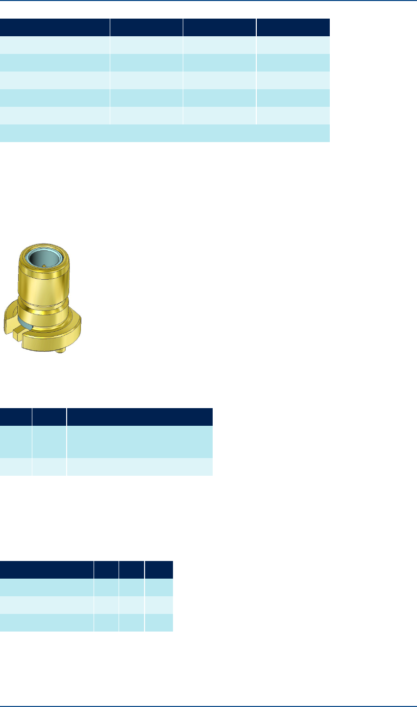
connector JAE SMB003D00 to provide cost efficient and robust interfacing for RF signal.
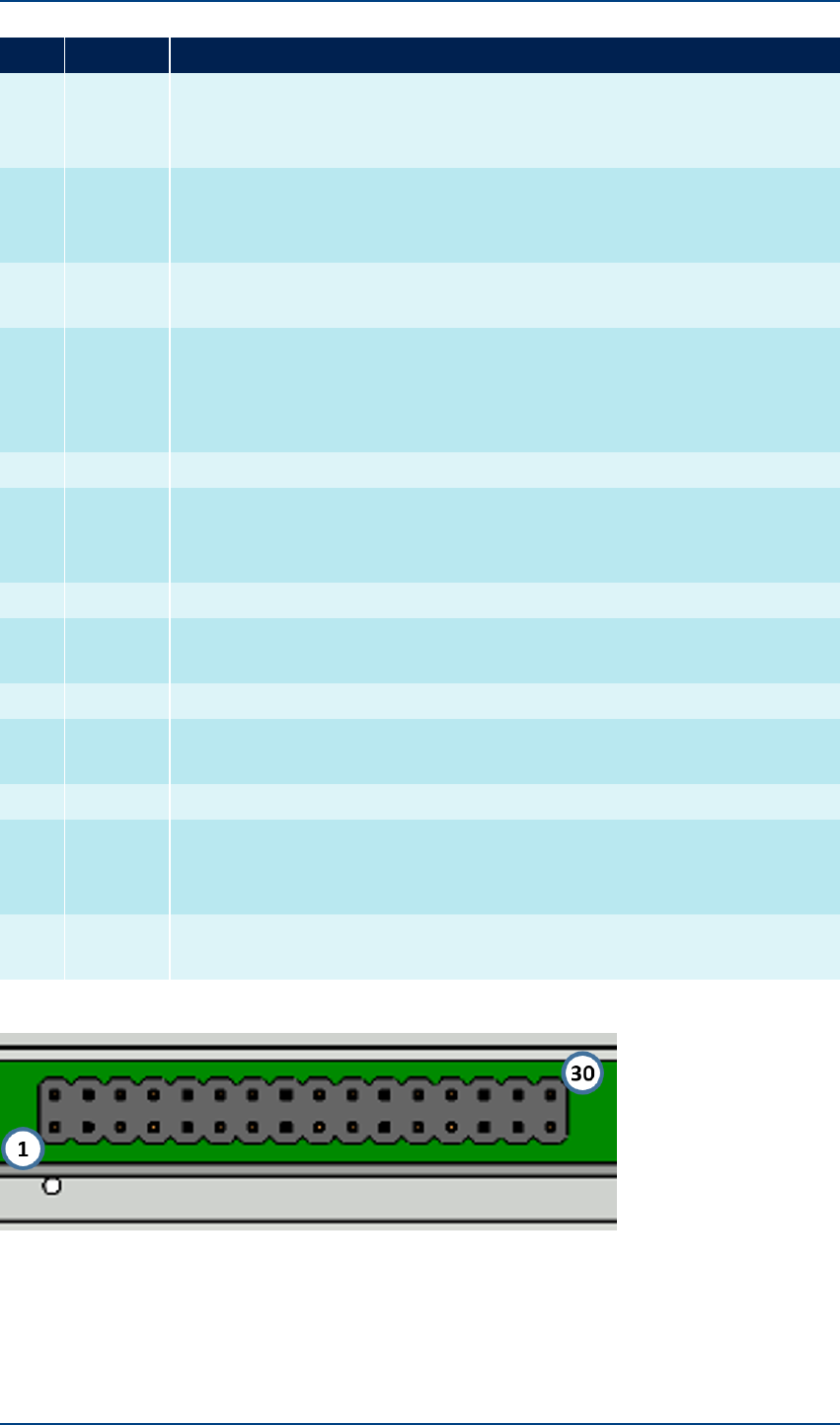
Figure 9
shows the connector used for GMR2 RF transceiver antenna interface.
Figure 9. GMR2 transceiver antenna interface connector
Signals in GMR2 transceiver antenna interface are connected as shown in
Table 10
.
Pin Signal Description
Center GMR RF Frequency: 1518 MHz – 1675 MHz
Power:
output +33,5 dBm MAX
input-10dBm MAX
Frame GND Signal GND
Table 10. GMR2 transceiver antenna interface pins
4.3.1.1:External antenna requirements.
External GMR antenna shall meet following baseline requirements (RF cable losses not included in
antenna gain figures). It shall be noted that actual antenna performance requirements are
dependent on terminal type (fixed, maritime etc). Detailed antenna requirements may be provided
by Inmarsat on request.
min max Unit
Frequency band 1518 1675 MHz
18:GSPS Core Module 2.0 VAM-CM HW Description
Confidential and Proprietary – Inmarsat Global Limited
inmarsat.com
DRAFT
4: VAM-CM interfaces
min max Unit
Pass band impedance 50 50 Ohms
Pass band gain 2 dBic
Extended band gain 0 dBic
Axial ratio 4 dB
Extended band Axial ratio 6 dB
Extended band frequencies: RX 1518…1525MHz, TX 1668…1675MHz
Table 11. GMR external antenna requirements
4.3.2:GPS receiver antenna interface
The GPS receiver Antenna interface uses snap on SMB connector JAE SMB003D00 to provide cost
efficient and robust interfacing for RF signal.
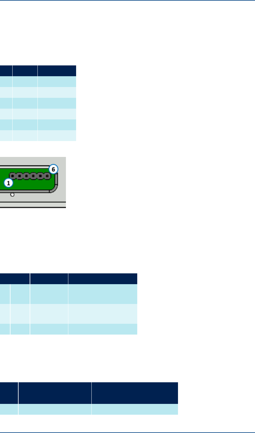
Figure 10
shows the connector used for GPS RF receiver
antenna interface.
Figure 10. GPS receiver antenna interface connector
Signals in GMR2 transceiver antenna interface are connected as shown in
Table 10
.
Pin Signal Description
Center GPS RF Frequency: 1575 MHz – 1605 MHz
Power: -20 dBm MAX
Frame GND Signal GND
Table 12. GPS receiver antenna interface pins
4.3.2.1:External GPS antenna requirements.
External GPS antenna shall meet following requirements (RF cable losses not included in antenna
gain figures).
min max Unit
Frequency band 1575 1605 MHz
Pass band impedance 50 50 Ohms
Pass band gain 0 dBi
Table 13. GPS external antenna requirements
19:GSPS Core Module 2.0 VAM-CM HW Description
Confidential and Proprietary – Inmarsat Global Limited
inmarsat.com
DRAFT
4: VAM-CM interfaces
4.4: VAM-CM Power Management Handling
The VAM-CM power management handling is based on VAM-CM control interface, UART or USB.
This is required to put CM in low power mode to reduce CM power consumption.
4.4.0.1:VAM-CM USB interface PM Handling
In the VAM-CM USB control interface, core module (CM) supports USB suspend/resume feature as
per USB2.0 standards to put in low power mode. By default low power mode is disabled in CM and
CM can be put into low power mode based on USB suspend signal and wakeup based on resume
signal, seeReferences on page 5 section 7.1.7.6 and 7.1.7.7. Without handling USB
suspend/resume the CM will not enter low power mode and hence overall current consumption will
be more. It is recommended that the VAM should implement USB suspend/resume feature to put CM
in low power mode and wakeup from low power mode.
4.4.0.2:VAM-CM UART interface PM Handling
In VAM-CM UART control interface, core module (CM) low power mode (sleep) is by default enabled
and VAM can get sleep state and wakeup from sleep state using VAM_CM_SLEEP and VAM_CM_
WAKEUPsignals. VAM can check CM sleep state using VAM_CM_NSLEEP signal, high=Active and
low=sleep. VAM need to check VAM_CM_SLEEP signal before sending any data to CM and if this
signal is low then set VAM_CM_WAKEUPsignal high for 100mSec to wakeup CM and ready to
process data. See
Table 9
for Sleep and Wake-up signal details.
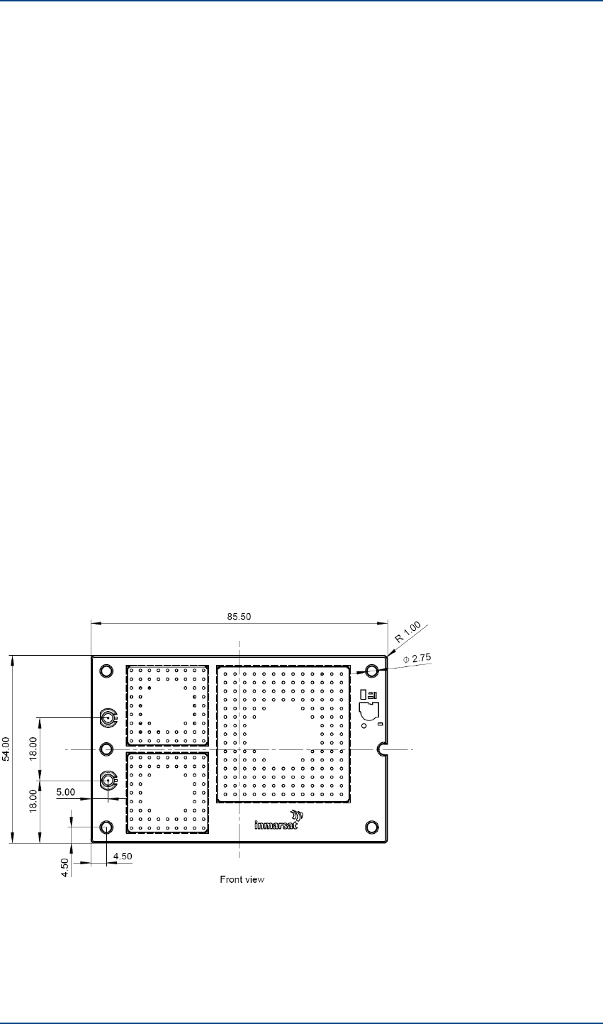
4.5: Mechanical interface
Mechanical dimensions and mounting points are shown in
Figure 11
-
Figure 13
. VAM-CM can be
mounted with four 2,5mm screws from the module corners. 5mm extension towers are required to
mount VAM-CM so that tightening the screws does not introduce any forge to components and shield
can soldered on the board.
Figure 11. Front view dimensions
20:GSPS Core Module 2.0 VAM-CM HW Description
Confidential and Proprietary – Inmarsat Global Limited
inmarsat.com
DRAFT
4: VAM-CM interfaces
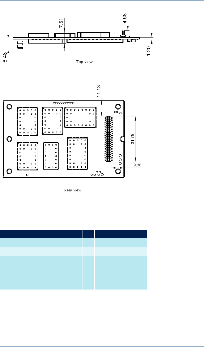
Figure 12. Side view dimensions
Figure 13. Rear view dimensions
4.6: Environmental conditions
Environmental operating conditions for VAM-CM are shown in
Table 14
.
Min Nominal Max Unit
Operating temperature -20 +25 +70 Celsius degrees
Humidity 0 90 %
Vibration 0,96
0,96
m2/s25 Hz to 20 Hz
m2/s220 Hz to 100 Hz
(30 minutes/axis)
(thereafter -3dB/octave)
Table 14. Environmental requirements
21:GSPS Core Module 2.0 VAM-CM HW Description
Confidential and Proprietary – Inmarsat Global Limited
inmarsat.com
DRAFT
5: Evaluation tools
5: Evaluation tools
This chapter gives more detailed information concerning the evaluation module and control software
included in evaluation kit.
5.1: Evaluation kit
The VAM-CM evaluation kit includes VAM-CM evaluation module, control software and
documentation. VAM terminal manufacturer can use evaluation kit to verify the VAM-CM functionality
by controlling VAM-CM directly with control SW. The evaluation kit also allows VAM terminal
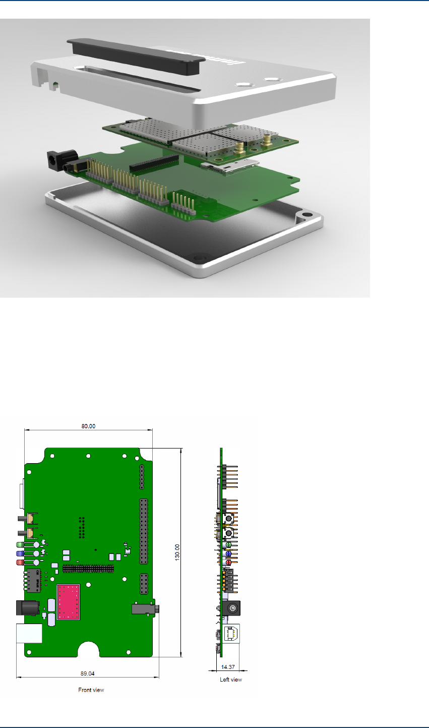
manufacturer to connect their own controller board to evaluation kit and verify planned interfaces.
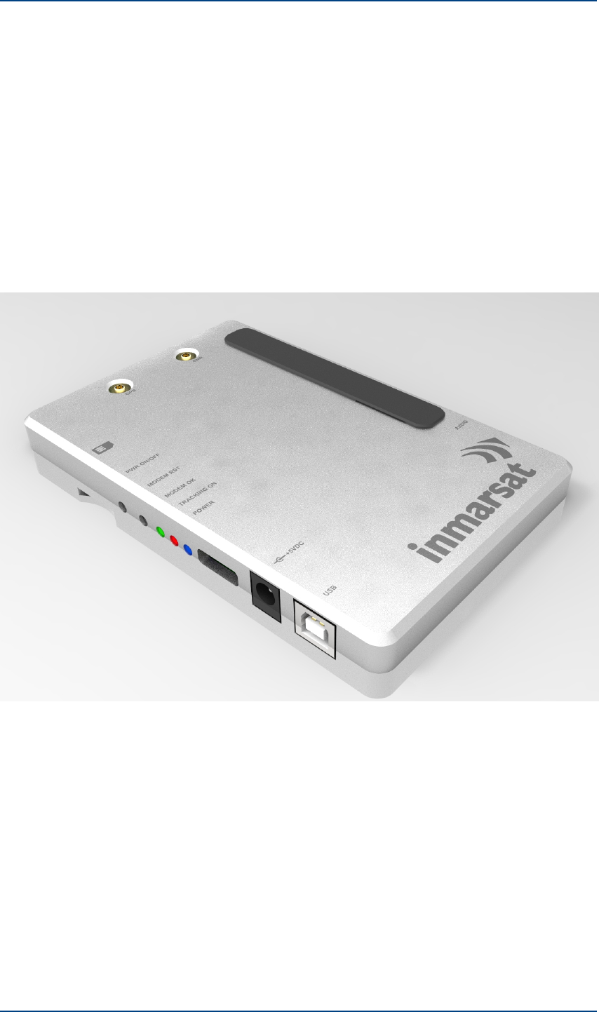
Figure 14
shows the simplified visualization of the evaluation module.
Figure 14. VAM-CM Evaluation module visualization
5.2: Evaluation module
The Evaluation module is built to ease handling and evaluation of VAM-CM product. Evaluation
module shown in
Figure 15
contains VAM-CM evaluation board and VAM core module packaged in a
simple mechanical structure. VAM-CM interfaces are extracted with VAM-CM evaluation board to
make interfacing and control of VAM-CM easier.
22:GSPS Core Module 2.0 VAM-CM HW Description
Confidential and Proprietary – Inmarsat Global Limited
inmarsat.com
DRAFT
5: Evaluation tools
Figure 15. VAM-CM Evaluation module break down
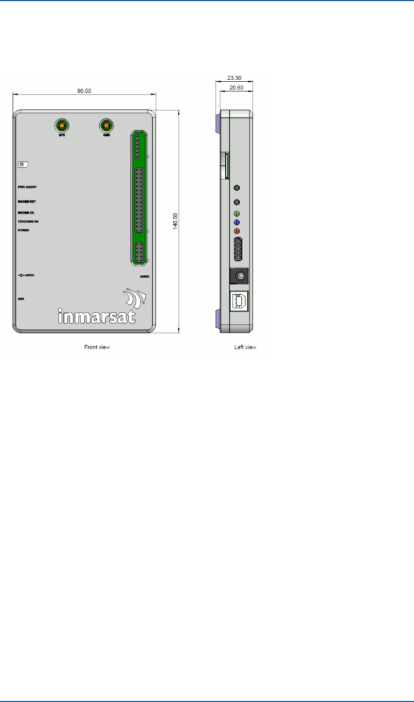
5.2.1:Evaluation module size
The evaluation board is designed to hold the VAM-CM module and standard interface connectors,
control switches and indicators. Dimensions of Evaluation board shown in
Figure 16
are 80mm by
130mm by 14,4mm excluding the extension length of parts reaching through the mechanical
structure.
23:GSPS Core Module 2.0 VAM-CM HW Description
Confidential and Proprietary – Inmarsat Global Limited
inmarsat.com
DRAFT
5: Evaluation tools
Figure 16. VAM-CM Evaluation board dimensions
Mechanical structure of evaluation module is milled aluminium. Dimensions of mechanical structure
shown in
Figure 17
are 90mm by 140mm by 20,6mm excluding the rubber feet.
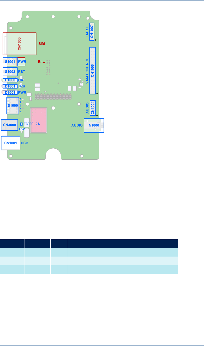
Figure 17. VAM-CM Evaluation module dimensions
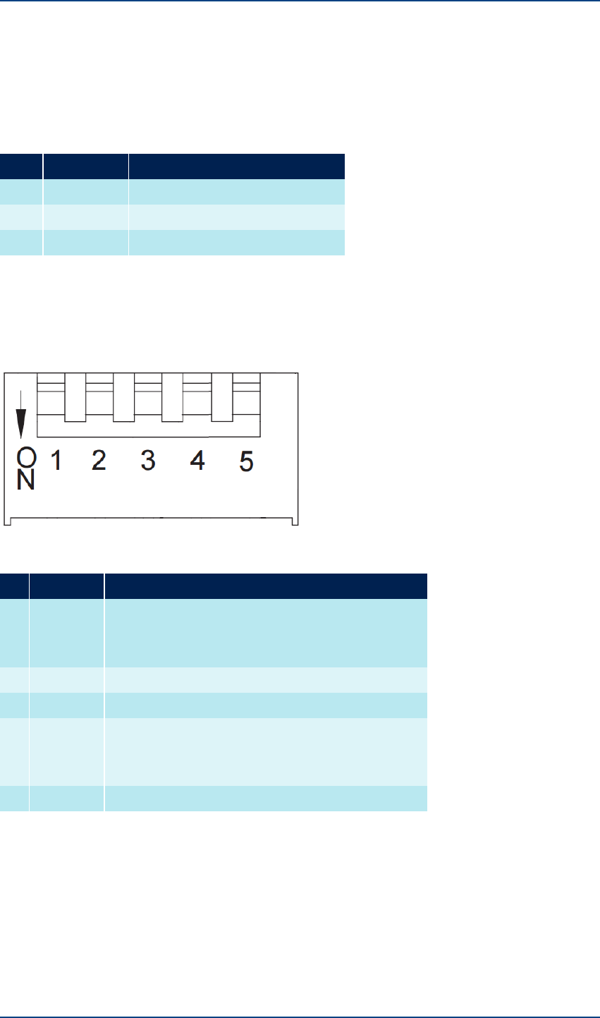
5.2.2:Evaluation module interfaces
This chapter describes the outer Indicators and interfaces of VAM-CM evaluation module. Interface
location can be seen in
Figure 18
. SIM socket and Boot switch are marked with red colour indicating
that component is at bottom side of the evaluation board. Other interfaces (marked with blue colour)
are located on top side of PWB.
Interfaces are designed so that basic interfacing can be done with standard connectors e.g. USB,
UART, SIM and Audio. In addition there are also pin headers to provide easier interfacing with
controller board.
24:GSPS Core Module 2.0 VAM-CM HW Description
Confidential and Proprietary – Inmarsat Global Limited
inmarsat.com
DRAFT
5: Evaluation tools
Figure 18. VAM-CM Evaluation module interface locations
Each interface is described in following chapters. Following chapters also indicate the special
arrangements when pin headers are applied instead of standard interfaces.
Pin numbers for signals are subject to change during R&D phase of the device.
5.2.2.1:Indicators
Evaluation module includes LED indicators showing the status information of the system. Available
status information is shown in
Table 15
.
Indicator Name Color Description
D3001 PWR ON BLUE Supply voltage for VAM-CM is active.
D1000 Modem OK GREEN VAM-CM Modem is active.
D1001 TTA Not OK RED VAM-CM active but does not have network connection
Table 15. Evaluation module indicators
5.2.2.2:Buttons and switches
The evaluation module includes control switches allowing the user to control the operations of the
VAM-CM. Controls are implemented with two push button switches S1001 for Power on/off and
S1002 Modem RST.
25:GSPS Core Module 2.0 VAM-CM HW Description
Confidential and Proprietary – Inmarsat Global Limited
inmarsat.com
DRAFT
5: Evaluation tools
Boot selection switch S2003 is located at bottom side of PWB available only with pin tool via small
hole in mechanics. This button is used to make VAM-CM to boot from USB device to start firmware
upgrade tool or enable direct USB flashing. Boot selection is required during R&D phase firmware
updates.
VAM-CM control buttons are shown in
Table 16
.
SW Control Description
S1001 PWR on/off Power on/off switching of VAM-CM.
S1002 Modem RST Warm reset for VAM-CM.
S2003 USB Boot SW Boot selection switch
Table 16. Evaluation module control buttons
5 way switch block S1000 allowing user to set-up and control the VAM-CM operation. Order of
switches in switch block is represented in
Figure 19
. Functions of included VAM-CM controls are
shown in
Table 17
.
Figure 19. Function order in control selector switch block
SW Control Description
#1 VAM Boot 1 Control interface selection during VAM-CM power-up.
"UP" – UART control active (default).
"DOWN" – USB control active
#2 Reserved
#3 Reserved
#4 TX Disable Disables transmitter operation of VAM-CM.
"UP" – Transmitter enabled (default).
"DOWN" – Transmitter disabled
#5 Reserved
Table 17. Evaluation module control selectors
Control switches and buttons are connected in parallel with VAM control interface. When evaluation
module is controlled via VAM control interface (pin header) all switches in S1000 shall be in "up"
position to allow VAM control interface to disable controls.
26:GSPS Core Module 2.0 VAM-CM HW Description
Confidential and Proprietary – Inmarsat Global Limited
inmarsat.com
DRAFT
5: Evaluation tools
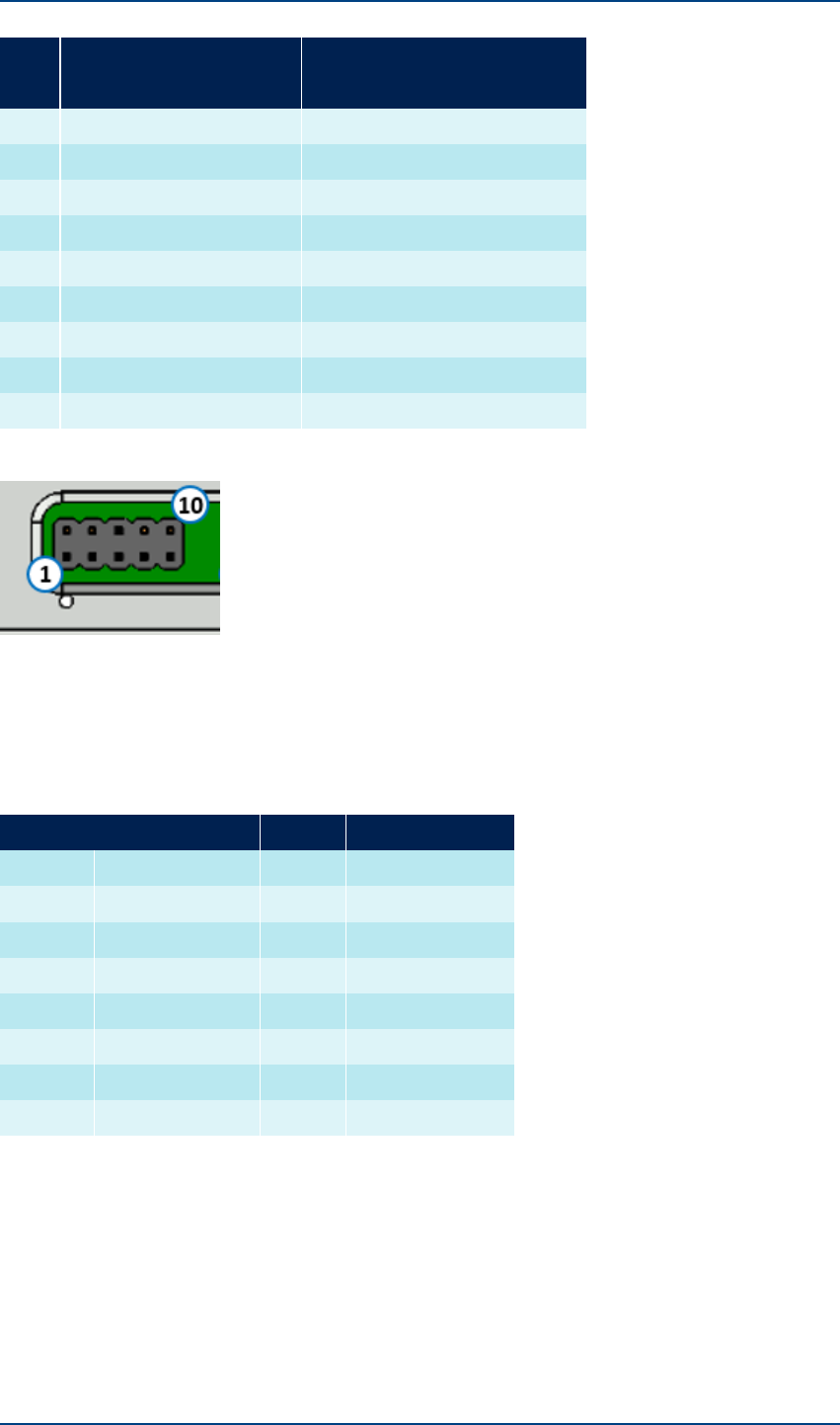
5.2.2.3:USB Interface
USB interface is implemented with Keystone Electronics 924 B-type USB connector CN-1001. Signal
order in connector is.
Pin Control Description
#1 VBUS USB Bus voltage
#2 Dm Negative data line
#3 Dp Positive data line
#4 GND
Table 18. USB interface signals
5.2.2.4:VAM control interface
The evaluation module control interface CN1005 includes most of VAM-CM controls. Only audio
interface is separated to its own pin header. VAM control interface enables connection of the SIM,
applying button and switch controls and getting the status of VAM-CM indicators.
VAM Power can also be supplied via the VAM control interface together with interface voltage Vio.
With Vio user can select suitable interface voltage level between 1,65V and 5,5v. Default 3,0V Vio is
supplied also in pin header and by default it is applied with jumper between pin #13 and #14. If
custom Vio is applied then jumper is removed and Vio is fed in pin #14 from external source.
The VAM control interface allows VAM terminal manufacturer to use external controller to adjust
VAM-CM settings. Control interface is 2 row 32 way pin header Harwin M20-9721645 which provides
following controls shown in
Table 19
. Pin organization is shown in
Figure 20
.
Pin Control Description
#1 …
#6
VBAT 3,9V supply for VAM-CM
#7 ...
#12
GND
#13 3,0V Vio
output
Power supply for Vio
#14 Vio input Supply input for Vio.
By default this is connected to pin #13
#15 Ext Vrtc
supply
External backup voltage supply to enable possibility to arrange external battery
backup supply for RTC and backup features.
3,3V (maximum load 1mA)
#16 VAM-CM
Wake-up
VAM-CM wake-up control input
“Rising edge” – Modem wake-up
#17 PWR on/off Power on/off switching of VAM-CM.
"LOW" 1 second pulse PWR on/off
"HIGH" (Float) no action
27:GSPS Core Module 2.0 VAM-CM HW Description
Confidential and Proprietary – Inmarsat Global Limited
inmarsat.com
DRAFT
5: Evaluation tools
Pin Control Description
#18 VAM_
MODEM_
OK
Modem OK
#19 Modem
RST
Warm reset for VAM-CM
"LOW" Warm reset for VAM-CM
"HIGH" (Float) no action
#20 TTA Not
OK
Modem has no GPS location or channel assignment
#21 VAM-
CMSleep
Indicates VAM-CM sleep mode status
“HIGH” – Modem Active
“LOW” – Modem Sleep
#22 SIM_V SIM supply voltage output
#23 VAM_
BOOT_1
Control interface selection (UART/USB) during power-up
"HIGH" (Float) UART control mode (default)
"LOW" USB control mode
#24 SIM_RST SIM Reset output
#25 VAM_
BOOT_2
Reserved for future use
#26 SIM_CLK SIM Clock output
#27 VAM_
BOOT_3
Reserved for future use
#28 SIM_IO SIM IO interface
#29 TX_
DISABLE
Disables VAM-CM transmitter operation
"HIGH" Transmission enabled in VAM-CM (default)
"LOW" Transmission disabled in VAM-CM
#30 CARD_
DETECT
SIM card inserted input
Table 19. VAM Control interface signals
Figure 20. VAM control interface pin organization
28:GSPS Core Module 2.0 VAM-CM HW Description
Confidential and Proprietary – Inmarsat Global Limited
inmarsat.com
DRAFT
5: Evaluation tools
5.2.2.5:UART Interface
UART interface is implemented with single row 6 way pin header CN1007. Applied interface is
commonly used interface and allows commercially available USB/UART cable e.g. FTDI TTL-232R-
3v3 adapter cable. Pin header type is Harwin M20-9730645. Signal order in pin header is shown in
following
Table 20
. Pin organization is shown in
Figure 21
.
Pin Control Description
#1 GND
#2 NC
#3 NC
#4 RXD Received data
#5 TXD Transmit data
#6 NC
Table 20. UART interface signals
Figure 21. UART interface pin organization
5.2.2.6:Audio interfaces
The evaluation module has two audio interfaces. Analog audio interface N1000 is 3,5mm standard
mono jack SJ-3523-SMT from CUI Inc providing audio in, audio out and GND. Signal order in analog
audio interface is shown in
Table 21
.
Pin Signal Description
#1 Tip an_Au Ext Ear Analog audio output
0.53Vrms (load 16 ohm)
#2 Ring an_Au Ext Mic Analog audio input
1.5 Vpp (0dBFS, 0dB gain)
#3 Sleeve An_Au GND
Table 21. Analog audio interface signals
Another audio interface XCN1004 is 2 row 10 way pin header Harwin M20-9720545 which provides
both analog and digital audio interfaces for VAM control. Signal order in pin header is shown in
Table
22
. Pin organization is shown in
Figure 22
.
Pin Signal Description
#10 AN_AUD_EXT_MIC Analog audio input
#1 AN_AUD_EXT_MIC Analog audio input
29:GSPS Core Module 2.0 VAM-CM HW Description
Confidential and Proprietary – Inmarsat Global Limited
inmarsat.com
DRAFT
5: Evaluation tools
Pin Signal Description
#10 AN_AUD_EXT_MIC Analog audio input
#2 AN_AUD_EXT_EAR Analog audio output
#3 AGND_1 GNDfor analog audio
#4 AGND_1 GNDfor analog audio
#5 GND GNDfor digital audio
#6 GND GND for digital audio
#7 DIG_AU_DX Digital audio transmit data
#8 DIG_AU_CLK Digital audio clock
#9 DIG_AU_DR Digital audio receive data
#10 DIF_AU_FS Digital audio frame sync
Table 22. Audio pin header interface
Figure 22. Audio pin header interface pin organization
5.2.2.7:SIM interface
The evaluation module SIM interface CN1006 is implemented with push-push type SIM socket Molex
47553-2001. Pin configuration of SIM interface is shown in
Table 23
.
Pin Control Description
#1 C1 VSIM SIM Supply voltage
#2 C5 SIM GND SIM GND
#3 C2 SIM RST SIM Reset
#4 C6 NC Not used
#5 C3 SIM CLK SIM Clock
#6 C7 SIM IO SIM data IO
#7 CD0 CD0 Card Detect
#8 … #10 CD1, GND0, GND1 GND
Table 23. SIM interface signals
When applying the VAM control interface SIM card shall be removed from SIM socket CN1006 to
avoid malfunctions.
5.2.2.8:Evaluation module Power supply interface
The power supply interface CN3000 for evaluation module is provided with standard DC socket Cliff
Electronics DC10A. Evaluation module has internal regulators which will provide supply for VAM-CM.
30:GSPS Core Module 2.0 VAM-CM HW Description
Confidential and Proprietary – Inmarsat Global Limited
inmarsat.com

DRAFT
5: Evaluation tools
Supply voltage requirement for evaluation module is 5V with 1A continuous current supply capability
(4A peak). Power supply interface is protected with 2A SMD fuse. Pin configuration of power supply
interface is shown in
Table 24
.
Pin Signal Description
#1 Center Vsupply +5 V, 4A peak
#2 Body GND GND
Table 24. ower supply interface signals
5.2.2.9:RF Interfaces
RF interfaces are connected directly to VAM-CM antenna connectors which are described in more
detail in Radio interface description on page 18.
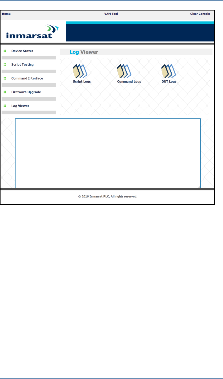
5.3: Control tools
The VAM control tool is based on web interface and back-end command server to interact with VAM
terminals. The VAM control tool enables the use of AT-commands and AT-command sequences to
control VAM terminal. Controls and DUT responses can be logged for future investigation.
The VAM control tool also contains simplified engineering mode enabling the possibility to control
receiver and transmitter independently. Simplified engineering mode allows turning on the
transmitter in dedicated channel and output power level as well as turning on the receiver in
dedicated channel and to measure RCER and RSSI of the input signal.
Figure 23
shows a screen shot of VAM control tool log viewer. More detailed information concerning
the VAM control tool can be found in
VAM Tool User Guide
.
31:GSPS Core Module 2.0 VAM-CM HW Description
Confidential and Proprietary – Inmarsat Global Limited
inmarsat.com