Inseego NVWE362 Cellular/PCS/GSM/EDGE/WCDMA/CDMA&700MHz LTE Module User Manual OEM Integration
Novatel Wireless Inc Cellular/PCS/GSM/EDGE/WCDMA/CDMA&700MHz LTE Module OEM Integration
UserManual.wiki
>
Inseego
>
NVWE362 User Manual
>
User Manual - OEM Integration
Contents
1.
Users Manual
2.
Users Manual per CRN96659
3.
Host user manual 1 of 3
4.
Host user manual 2 of 3
5.
Host user manual 3 of 3
6.
User Manual - OEM Integration
7.
User Manual - Host
8.
User Manual
User Manual - OEM Integration
Navigation menu
Upload a User Manual
Namespaces
Wiki Guide
HTML
PDF
Info
Views
User Manual
Discussion / Help
Navigation
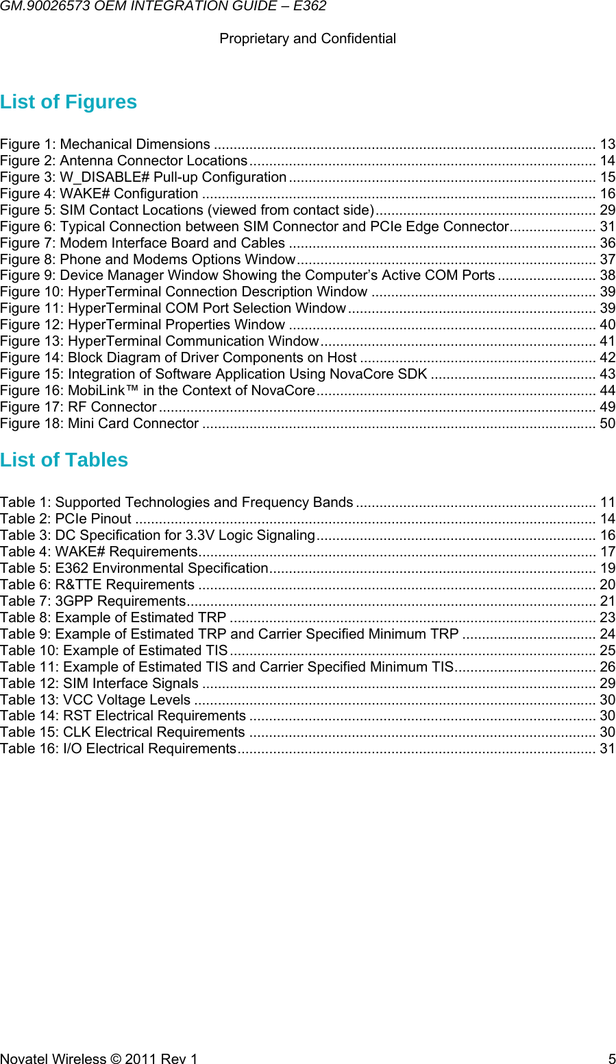

![GM.90026573 OEM INTEGRATION GUIDE – E362 Proprietary and Confidential Novatel Wireless © 2011 Rev 1 7Reference Documents [1] PCI Express Mini Card Electromechanical Specification, Revision 1.2, October 26, 2007. [2] PCI Express Card Electromechanical Specification revision 1.1 March 28th 2005 [3] SMBus Specification, Revision 2.0 [4] The I2C BUS SPECIFICATION Version 2.1 January 2000 [5] TS 36 series specifications on LTE http://www.3gpp.org/ftp/Specs/html info/36 series.htm [6] 3GPP TS 01.04: "Abbreviations and acronyms". [7] 3GPP TS 11.11: “Specification of the Subscriber Identity Module Mobile Equipment (SIM ME) interface”. [8] 3GPP TS 11.12: "Specification of the 3 Volt Subscriber Identity Module Mobile Equipment (SIM ME) interface". [9] 3GPP TS 11.18: “Specification of the 1.8 Volt Subscriber Identity Module Mobile Equipment (SIM ME) interface”. [10] 3GPP TS 51.010 1 “Mobile Station (MS) conformance specification; Part 1: Conformance specification”. [11] 3GPP TS 23.040: "Technical realization of the Short Message Service (SMS) ". [12] 3GPP TS 23.041: "Technical realization of the Cell Broadcast Service (CBS)". [13] 3GPP TS 24.008: "Mobile Radio Interface Layer 3 specification; Core Network Protocols; Stage 3". [14] 3GPP TS 24.011: "Short Message Service (SMS) support on mobile radio interface". [15] 3GPP TS 24.012: "Cell Broadcast Service (CBS) support on the mobile radio interface". [16] 3GPP TS 27.001: "General on Terminal Adaptation Functions (TAF) for Mobile Stations (MS)". [17] 3GPP TS 27.007: "AT command set for User Equipment (UE)". [18] 3GPP TS 51.011: "Specification of the Subscriber Identity Module Mobile Equipment (SIM ME) interface". [19] ITU T Recommendation V.25ter: "Serial asynchronous automatic dialing and control". [20] ITU T Recommendation V.24: "List of definitions for interchange circuits between data terminal equipment (DTE) and data circuit terminating equipment (DCE)". [21] ITU T Recommendation E.164: "The international public telecommunication numbering plan". [22] ITU T Recommendation E.163: "Numbering plan for the international telephone service". [23] 3GPP TR 21.905: "Vocabulary for 3GPP Specifications". [24] 3GPP TS 31.102: "Characteristics of the USIM application. [25] 3GPP TS 23.038: "Alphabets and language specific information". [26] High Speed USB Platform Design Guidelines, Intel, Rev. 1.0, dt. 07/12/2000, [27] 3GPP TS 11.12: "Specification of the 3 Volt Subscriber Identity Module Mobile Equipment (SIM ME) interface".](https://usermanual.wiki/Inseego/NVWE362.User-Manual-OEM-Integration/User-Guide-1901081-Page-8.png)
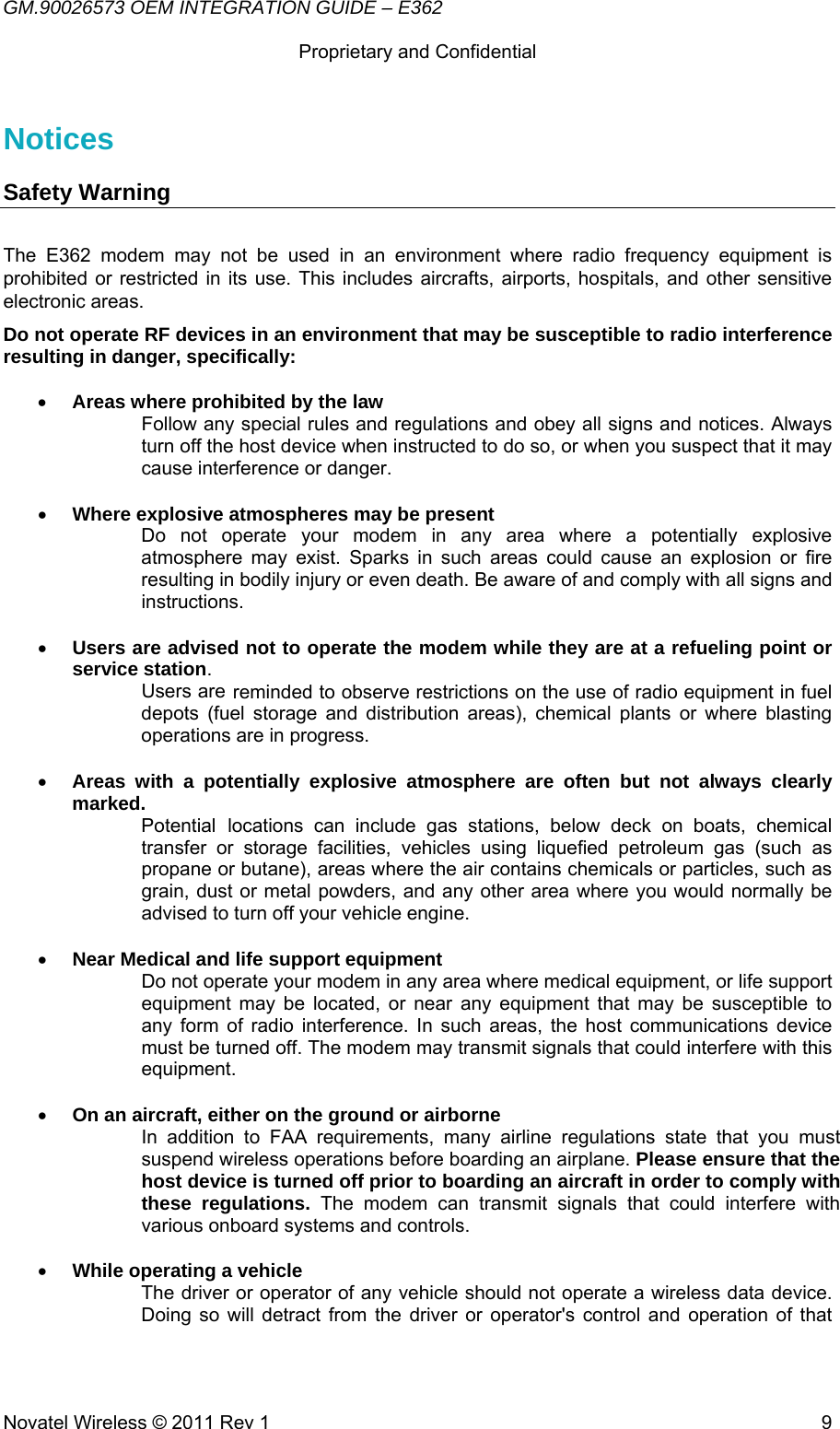
![GM.90026573 OEM INTEGRATION GUIDE – E362 Proprietary and Confidential Novatel Wireless © 2011 Rev 1 8[28] 3GPP TS 11.18: “Specification of the 1.8 Volt Subscriber Identity Module Mobile Equipment (SIM ME) interface”. [29] 3GPP TS 51.010 1 “Mobile Station (MS) conformance specification; Part 1: Conformance specification”. [30] ISO/IEC 7816 1: “Identification cards – Integrated circuit cards with contacts – Part 1: Physical characteristics”. [31] ISO/IEC 7816 2: “Identification cards – Integrated circuit cards with contacts – Part 2:Dimensions and locations of the contacts. [32] ISO/IEC 7816 3 “Identification cards – Integrated circuit cards with contacts – Part 3: Electronic signals and transmission protocols”. [33] Compliance Test Plan: LTE over the air Radiated Performance, version 6.0, Verizon Wireless, September 2010.](https://usermanual.wiki/Inseego/NVWE362.User-Manual-OEM-Integration/User-Guide-1901081-Page-9.png)
![GM.90026573 OEM INTEGRATION GUIDE – E362 Proprietary and Confidential Novatel Wireless © 2011 Rev 1 111. Overview of LTE Module E362 The E362 modem is part of the Novatel Wireless’ Expedite® PCI Express Mini Card family of modules. This module is capable of providing the terminal side interface of an LTE Network. The modem is designed to support the LTE terminal devices to be connected primarily to the Verizon Wireless Network in the U.S.A. In addition to LTE, the E362 modem supports 3G and 2G wireless technologies such as HSPA+ / EDGE / GPRS, CDMA EVDO DO Revision 0 and Revision A, and CDMA 1xRTT. The modem has been developed to be integrated into devices such as Notebook PCs, Notebook Tablet PCs, hand held devices, etc., and are based on the PCI Express Mini card specification 1.2 [1]. Following are the bands in which the E362 module is operational for each wireless technology. Table 1: Supported Technologies and Frequency Bands System Band Band Name Uplink (MHz) Downlink (MHz) CDMA BC0 Cellular 824 – 849 869 - 894 BC1 pcs 1850 – 1910 1930 - 1990 GPRS/EDGE 850 Cellular 824 – 849 869 – 894 900 900 880.0 – 914.8 925.0 – 959.8 1800 DCS 1710.2 – 1784.8 1805.2 – 1879.8 1900 PCS 1850 – 1910 1930 – 1990 HSPA+ V Cellular 824 – 849 869 – 894 VIII 900 880 – 915 925 – 960 II PCS 1850 – 1910 1930 – 1990 I IMT 1920 – 1980 2110 – 2170 LTE XIII Verizon 700 777 – 787 746 – 756 GPS L1 GPS NA 1565.19 – 1585.65 L1 Glonass 1598.06 – 1605.94 The design of the module is based on the MDM9600 chipset of Qualcomm™. This chipset supports Equalizer and Receive Diversity technologies. The Equalizer technology reduces the inter symbol interference caused by multi paths. The receiver diversity helps to retrieve signals under deep fades caused by multi paths. The E362 modem is compatible with Microsoft Windows™ compliant applications including VPN, email, and web browsing. The core protocol stack of this modem is supplied by Qualcomm™ and it contains software modules for supporting LTE, UMTS, HSDPA, GPRS/EDGE and CDMA technologies. Around this core, Novatel Wireless has created Firmware Drivers that provide access for the host to the hardware of the embedded modem. Accordingly, the feature set of the modem comprise data device features supported in the Qualcomm™ protocol stack and the features implemented by Novatel Wireless in the Drivers. The list of key features is as follows: • LTE • HSDPA/UMTS • EDGE/GPRS class 12 • Quad band GPRS/EDGE 850/900/1800/1900 • CDMA 1xRTT, EVDO Rev. 0, and Rev. A](https://usermanual.wiki/Inseego/NVWE362.User-Manual-OEM-Integration/User-Guide-1901081-Page-12.png)
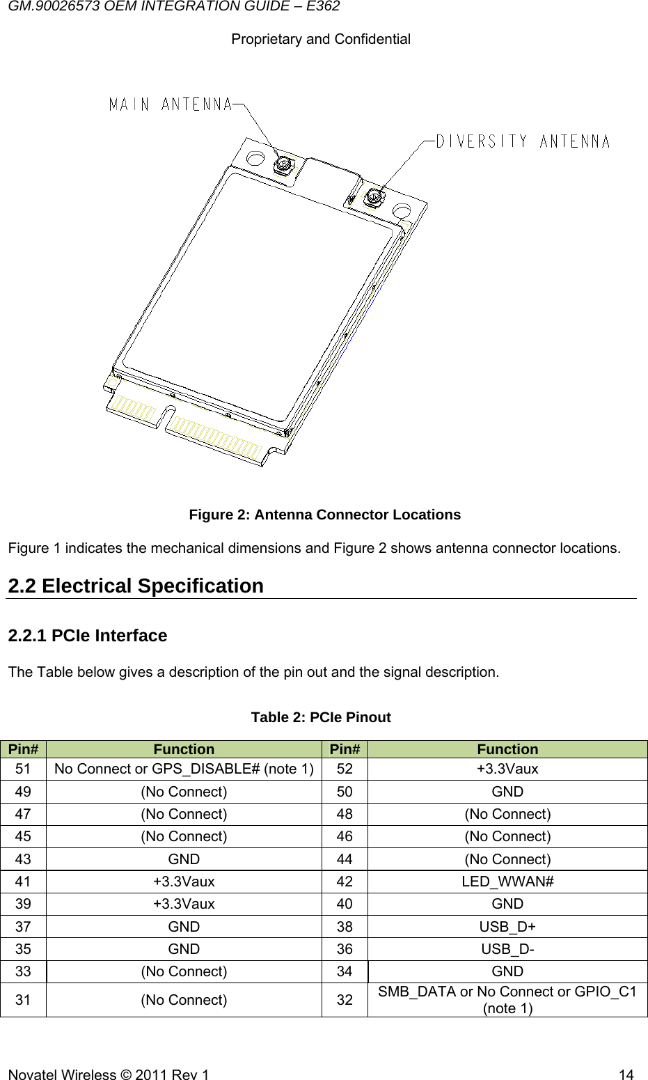
![GM.90026573 OEM INTEGRATION GUIDE – E362 Proprietary and Confidential Novatel Wireless © 2011 Rev 1 132. Module Specification As was described in the previous Section, the E362 modem has been designed in accordance with the PCI Express Mini Card Specification 1.2 [1]. The governing body for PCI Express standardization is PCI SIG (Peripheral Component Interconnect Special Interest Group).The website for PCI SIG can be found at the following URL: www.pcisig.com/home The E362 modem provides platform developers and system integrators with the ability to enable 4G/3G/2G wireless broadband access. The modem you have obtained may have undergone certain customization specific to your requirement. These customizations are carried out with respect to certain reserved pins as specified in the PCI Express Mini Card Specification. By using these reserved pins, a user of the customized modem may be able to implement certain functions that are outside the scope of the PCI Express Mini Card specification. In that respect, the specification of the modem module you have obtained might differ from the generic specification of the E362 modem. The important topics of the specification required for the integration of this modem into host devices are given below: 2.1 Mechanical Specification The E362 modem meets the form factor as specified by the PCI Express Full Mini Card Electromechanical Specification Revision 1.2 Type F2. Figure 1: Mechanical Dimensions](https://usermanual.wiki/Inseego/NVWE362.User-Manual-OEM-Integration/User-Guide-1901081-Page-14.png)
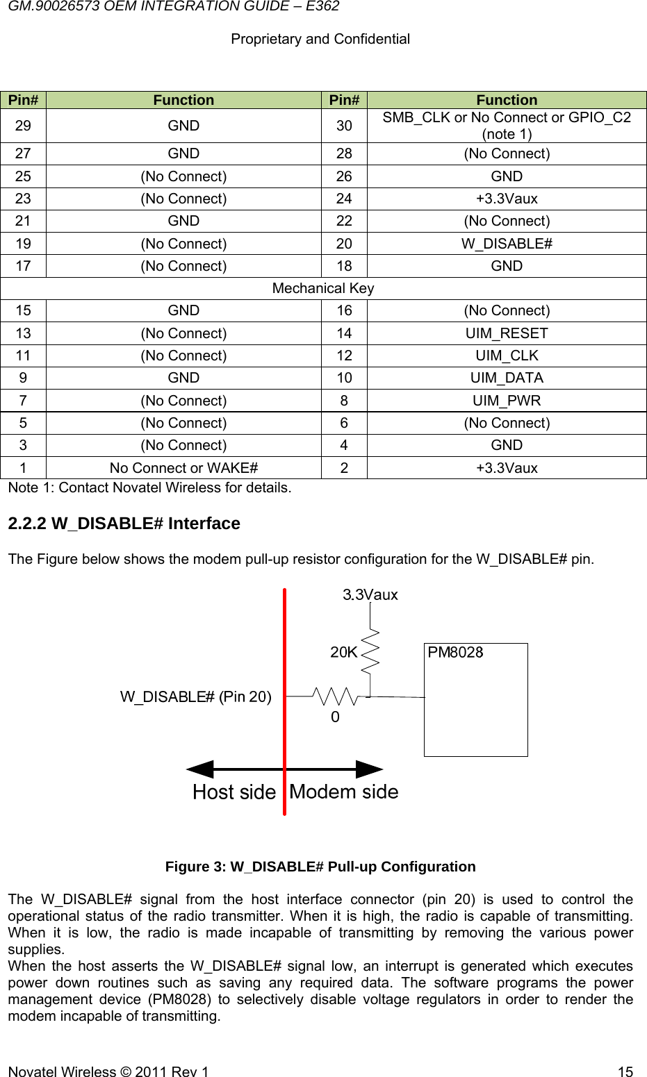
![GM.90026573 OEM INTEGRATION GUIDE – E362 Proprietary and Confidential Novatel Wireless © 2011 Rev 1 16 The assertion and de-assertion of W_DISABLE# is asynchronous to any system clock. The modem meets the logic signal requirements as defined in Table 3-7 of the PCI Express Mini Card Specification 1.2 [1]. The table below is shown for reference, and lists the 3.3V card logic levels for the W_DISABLE# signal. Table 3: DC Specification for 3.3V Logic Signaling Symbol Parameter Conditions Min Max UnitsNotes+3.3Vaux Supply Voltage 3.3 – 9% 3.3 + 9% V 1 VIH Input High Voltage 1.95 3.6 V VIL Input Low Voltage -0.5 0.8 V IIN Input Leakage Current 0V to 3.3V -10 +10 µA ILKG Output Leakage Current 0V to 3.3V -50 +50 µA CIN Input Pin Capacitance 7 pF NOTES: 1. As measured at the card connector pad. 2. The W_DISABLE# signal is falling edge triggered. 3. The W_DISABLE# signal cannot be driven high if the module is not powered. 2.2.3 WAKE# Interface The WAKE# signal is an open collector, active low signal. It is used to request that the host system return from a sleep/suspended state to service a function initiated wake event. If the wakeup process is implemented in the host platform, a host pull-up resistor (≥ 5kΩ recommended) tied to no higher than +3.3Vaux is required on this pin. The Figure below shows the modem configuration. Figure 4: WAKE# Configuration NOTE to Figure 4: The DTC114EB device may be changed to an equivalent device without prior notice. Contact Novatel Wireless for details.](https://usermanual.wiki/Inseego/NVWE362.User-Manual-OEM-Integration/User-Guide-1901081-Page-17.png)
![GM.90026573 OEM INTEGRATION GUIDE – E362 Proprietary and Confidential Novatel Wireless © 2011 Rev 1 21R&TTE Requirement Discipline Definition Applied Standard EN 301 908 21 The E362 modem complies with the applicable 3GPP standards for LTE, CDMA, WCDMA/HSDPA and GPRS/EDGE listed in the Table below. Table 7: 3GPP Requirements Source Standard Title/Description Document Number 3GPP WCDMA / HSDPA / GPRS / EDGE [UMTS] User Equipment (UE) Radio Transmission and Reception (FDD) TS 25.101 3GPP LTE [LTE] Evolved Universal Terrestrial Radio Access (E-UTRA); User Equipment (UE) Radio Transmission and Reception TS 36.101 3GPP2 CDMA Recommended Minimum Performance Standards for cdma2000 Spread Spectrum Mobile Stations TIA-98-F 3GPP2 CDMA Recommended Minimum Performance Standards for cdma2000 High Rate Packet Data Access TIA-866-1 3GPP2 CDMA Recommended Minimum Performance Standards for cdma2000 High Rate Packet Data Access TIA-866-A Apart from the compliance requirements of FCC and CE as described above, there are many carrier specific compliance requirements that the modem needs to satisfy. A summary of these requirements and a brief description of them are given in Appendix A. 1 Electromagnetic compatibility and Radio Spectrum Matters (ERM) Base Stations (BS) and User Equipment (UE) for IMT 2000 Third Generation cellular networks. Part 2: Harmonized EN for IMT 2000, CDMA Direct Spread (UTRA FDD) (UE) covering essential requirements of article 3.2 of the R&TTE Directive](https://usermanual.wiki/Inseego/NVWE362.User-Manual-OEM-Integration/User-Guide-1901081-Page-22.png)
![GM.90026573 OEM INTEGRATION GUIDE – E362 Proprietary and Confidential Novatel Wireless © 2011 Rev 1 24Table 9: Example of Estimated TRP and Carrier Specified Minimum TRP Disclaimer: This spread sheet is provided with no warranties whatsoever. Novatel disclaims all liability relating to the use of information in this specification. Note that this table is provided for rough estimation purposes only and is intended to provide a first pass guideline for antenna loss planning. It is not to be a substitute for detailed design activity. Additional losses, efficiency considerations and other system affects will modify the actual resulting TIS and as such results will deviate from the TRP calculator shown above. All Cingular, Vodafone, Verizon & Sprint TIS requirements are subject to change and as such Novatel makes no claim to accuracy. Updates to TIS limits are not controlled in this document. 3.1.2 Total Isotropic Sensitivity (TIS) To obtain the TIS of the receiver part of the UE, the sensitivity of the UE is measured over a spherical surface surrounding the UE, similar to the measurement carried out for obtaining the TRP. The sensitivity is a performance metric which represents the minimum power level at which the error rate of the receiver is better than a specific limit. Depending on the radio technology, this limit may be specified on Bit Error Rate (BER), Block Error Rate (BLER) or a Frame Error Rate (FER) or throughput reduction. Sensitivity is measured by lowering the transmit power level of the Base Station Simulator until the specified limit is reached. The power level at the antenna connector of the module required to keep the error rate less than the specified limit is the value of sensitivity. In Section 3.1.2 of Reference [33], it has been indicated that the sensitivity is the power level at the antenna connector at which the throughput falls to 95% of the maximum Band Carrier #1 dBm Carrier #2 dBmMinimum limit of TRP stipulated by Verizon WirelessRequired enhancement in TRP-performance (dBm)LTE Band 13 777-787 MHz. (Tx) 746-756 MHz. (Rx)18 N/ACellular 824-849 (Tx) 869-894 (Rx)20 -0.30PCS 1850-1910 (Tx) 1930-1990 (Rx)20 -0.30Band I 2100 Band II 1900Band IV 850GSM850GSM900GSM1800GSM1900Carrier-TRP-Limits and Required performance-improvement](https://usermanual.wiki/Inseego/NVWE362.User-Manual-OEM-Integration/User-Guide-1901081-Page-25.png)
![GM.90026573 OEM INTEGRATION GUIDE – E362 Proprietary and Confidential Novatel Wireless © 2011 Rev 1 25throughput of the reference channel. For details on this reference channel, please see Table 3.1.2.2 of Reference [33]. In this Table, it is indicated that the tests would be conducted for a given number of Resource Blocks. Levels of maximum throughput for these tests are indicated in this Table. 3.1.2.1 TIS (Total Isotropic Sensitivity) Estimator TIS can generally be estimated by subtracting the losses and the de sense noise from the conducted sensitivity. The losses include cable loss and the loss on account of antenna efficiency. The desense noise is the noise level in the environment around the UE. A basic spreadsheet estimator1 can be used to estimate the TIS as indicated below in Table 10. As was described in Section 3.1.1, for example purposes only, we shall consider only the TIS requirement of Verzion Wireless for the LTE technology and the EVDO technology. The estimation of TIS and the required improvement are carried out in Table 10 and in Table 11. In Table 10, TIS is estimated from the known values. In Table 11, the improvement required for meeting the limit stipulated by Verizon is estimated. From the typical results in Table 11, it is seen that the radiated power is to be improved by 0.66 dBm in the LTE band, by 1.51 dBm in the cellular band, and 2.01 dBm in the PCS band. Reducing the loss over the cable and the connector, and increasing the efficiency of the antenna are the approaches to enhance the TIS performance. Table 10: Example of Estimated TIS Band Technology Conducted Sensitivity SpecConducted Sensitivity (dBm)Cable + Connector Loss (dB)PC Noise* Rise over Thermal (dB)Antenna Efficiency without Cable%Estimated TIS - Noise Free (dBm)LTE Band 13 777-787 MHz. (Tx) 746-756 MHz. (Rx)LTE 10MHz. BW -93.3 -97.2 0.85 3 50 -90.34Cellular Band 5 824-849 MHz. (Tx) 869-894 MHz. (Rx)EV-DO -104 -108 1 3 50 -101.0PCS Band 3 1850-1910 MHz. (Tx) 1930-1990 MHz. (Rx)EV-DO -104 -107.5 1 3 50 -100.5Band I 2100 MHz. WCDMA -106.7 -109 1 3 50 -102.0Band II 1900 MHz. WCDMA -104.7 -109 1 3 50 -102.0Band IV 850 MHz. WCDMA -104.7 -109 1 3 50 -102.0GSM850 GPRS -99 -108 1 3 50 -101.0GSM900 GPRS -99 -108 1 3 50 -101.0GSM1800 GPRS -97 -108 1 3 50 -101.0GSM1900 GPRS -99 -108 1 3 50 -101.0TIS Estimator for Embedded Modules in Jammer Free Environment Disclaimer: This spread sheet is provided with no warranties whatsoever. Novatel disclaims all liability relating to the use of information in this specification. Note that this table is provided for rough 1 Disclaimer: This spread sheet is provided with no warranties whatsoever. Novatel disclaims all liability relating to the use of information in this specification. Note that this table is provided for rough estimation purposes only and is intended to provide a first pass guideline for antenna loss planning. It is not to be a substitute for detailed design activity. Additional losses, efficiency considerations and other system affects will modify the actual resulting TIS and as such results will deviate from the TIS calculator shown above. Updates to TIS limits are not controlled in this document.](https://usermanual.wiki/Inseego/NVWE362.User-Manual-OEM-Integration/User-Guide-1901081-Page-26.png)
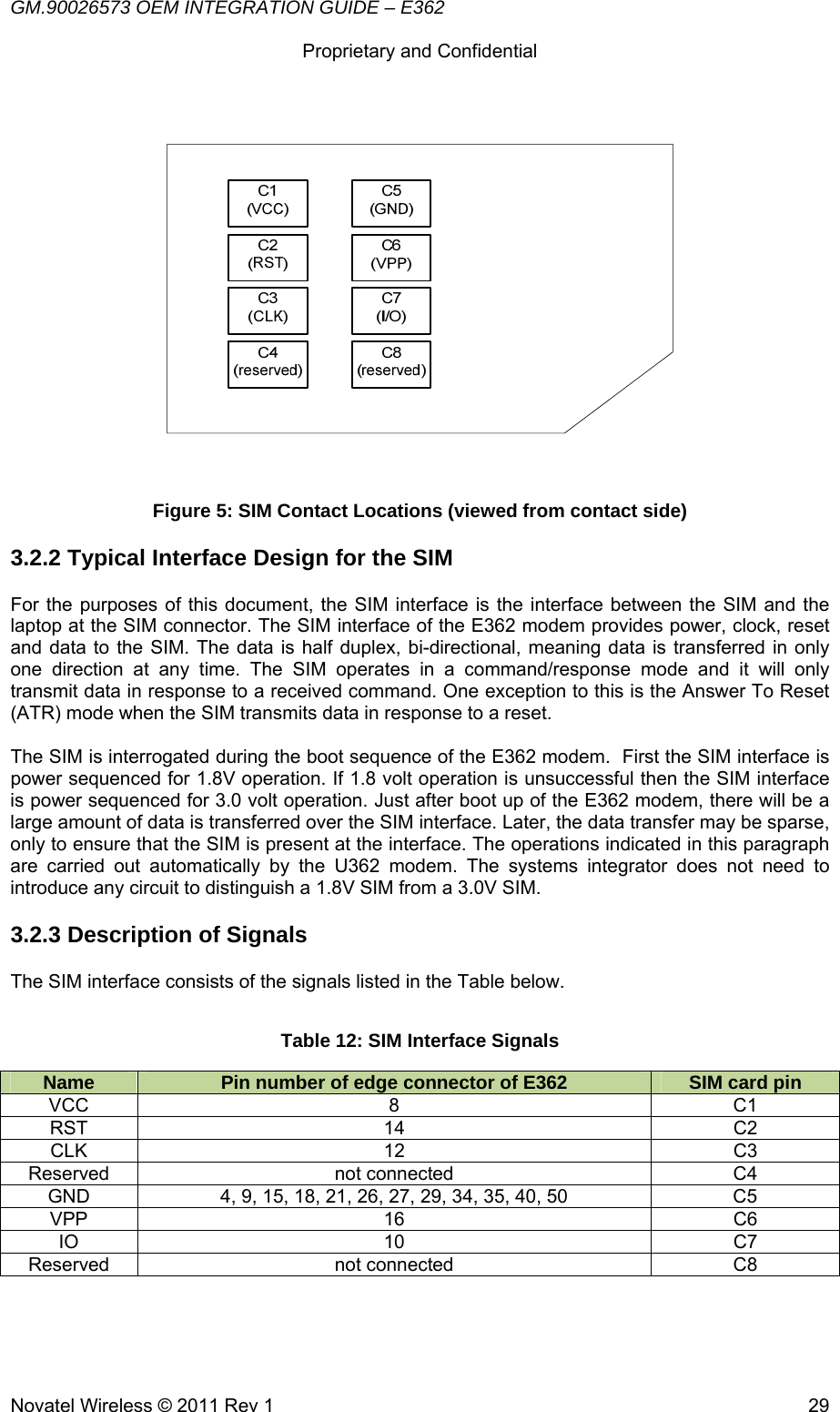
![GM.90026573 OEM INTEGRATION GUIDE – E362 Proprietary and Confidential Novatel Wireless © 2011 Rev 1 28• Connect the module to host device’s motherboard via two conductive screws, • If possible, place the module in a location that affords airflow, • Place a conductive tape between host device’s motherboard and the module. On the motherboard, remove the solder mask so that the conductive tape is directly in physical contact with the copper layer of the ground plane. Provide a large number of vias which would conduct the heat from the tape to inner ground planes. 3.1.3.6 Noise Mitigation Noise mitigation is essential in order to avoid the interference by the electronics on the host motherboard with the RF circuits of the module. This interference can degrade the module’s sensitivity and therefore its dynamic range and usability. Section 1 lists the frequency bands where the module’s receivers operate. Every effort should be made to ensure that there is no host induced noise in these frequency bands. Important design considerations to avoid interference include: • Selection of clock frequencies for the host motherboard for which the fundamental and harmonics fall outside the frequency bands mentioned above. For example: a 196MHz clock would have a 10th harmonic at 1960MHz, which is at the center of the 1900 CDMA/WCDMA/GSM band.. Simply shifting the clock frequency on the host motherboard to 190MHz would avoid any interference. • Decoupling the RF frequency at the output of power supplies. • Providing shielding layers around high speed clock traces by using multi-layer PCBs and/or shield cans. • Routing the antenna cables away from noise sources on the host motherboard. As shown in the Bottom view of the module indicated in Figure 1, there is a cut-out on the shield of the modem, close to the edge connector. It is recommended that traces on the host motherboard be routed away from this area. The intent is to reduce coupling from any noise that may be radiating from this slot. 3.2 Guidelines for integration of SIM 3.2.1 Description of SIM The SIM contains information related to subscriber identification, specification and authentication. With reference to the operating voltage, there are two different types of SIMs; one whose reference voltage is 1.8V and the other whose reference voltage is 3.0V. The physical size and contact location for the “Plug in SIM” format is defined in reference [7]. For the SIM connector, the contact identification is defined in reference [8]. Electrical characteristics for a 3V SIM are defined in Reference [8], and for a 1.8V SIM in reference [9]. Power sequencing and general protocol operation are defined in reference [32]. The figure below shows a “Plug in SIM” and its contact locations.](https://usermanual.wiki/Inseego/NVWE362.User-Manual-OEM-Integration/User-Guide-1901081-Page-29.png)
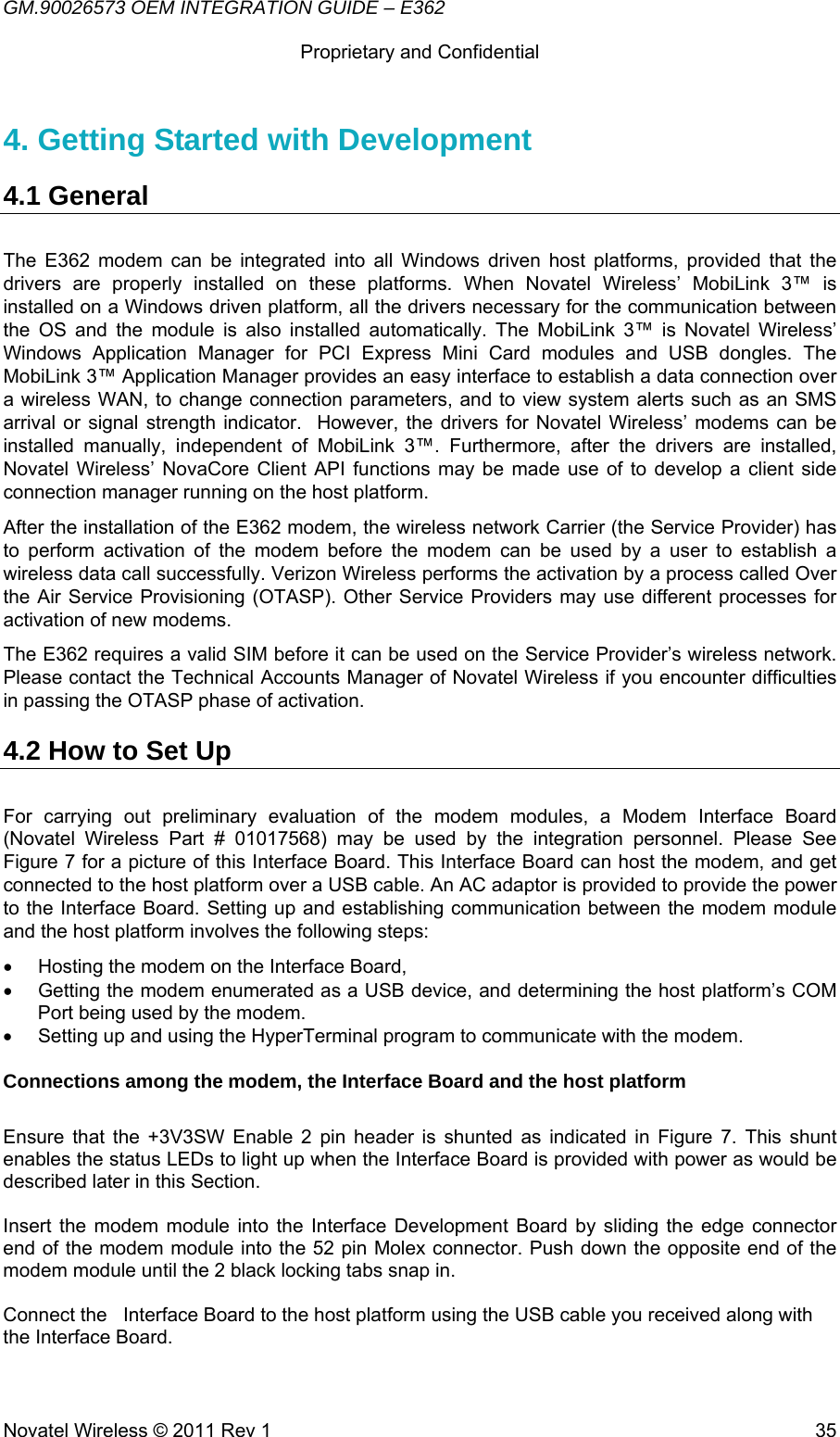
![GM.90026573 OEM INTEGRATION GUIDE – E362 Proprietary and Confidential Novatel Wireless © 2011 Rev 1 32Capacitors C1, C2, C3 C1, C2 and C3 are not to be populated. They exist if additional filtering is required. These components should be placed close to the SIM connector. Resistor R1, R2 R1 and R2 should be zero ohms. They exist if additional filtering is required. Resistor R3 R3 is shown in the circuit as a place holder so that the I/O signal can be pulled up if required. ESD protection Diode array DS1 DS1 should be a low capacitance ESD diode array (5 pF or less). It is important to minimize the capacitance on the I/O line so data performance is not degraded (deterioration of rise and fall times). DS1 should be placed close to the SIM connector. It is recommended that DS1 meets the limits of IEC61000 4 2, level 4 (±15kV air discharge, ±8kV contact discharge). Signal routing The CLK line is a high speed digital signal and care must be taken to ensure it is isolated from other signals. A guard trace should be used between the CLK trace and adjacent traces. A multi-layer PCB with a ground plane should be used. The CLK trace should be routed in an inner layer. CLK traces should be as short, and direct as possible, with no vias. All SIM card interface signals should be routed carefully to avoid being corrupted by each other or external signals. Capacitor on I/O signal trace In order to function properly, there is a limit on the amount of capacitance per signal line. The maximum capacitance added by the host (trace plus components) must not exceed 15pF per signal. Series resistance on the I/O signal trace I/O traces may also have a pull up on the I/O signal, which would allow sinking of 1 mA into the host motherboard when the I/O signal is driven low by the host motherboard. Series resistance for the I/O signal must be kept very low as the voltage drop across it may cause the output voltage at the connectors to be outside the specified limits. 3.2.4 Certification Since the SIM card interface is unique to each Notebook PC, the SIM card and Notebook PC together need to undergo several tests for obtaining certification. The electrical test cases are specified in section 27.17.2 in Reference [29]. 3.3 Guidelines for Integration of SMBus In this Section, the SMBus interface of the E362 modem is described. A 2 line SMBus is supported in hardware, but SMBus is not implemented in firmware other than test provisioning. It may be customized based on customer requirements but would require Novatel Wireless firmware effort.](https://usermanual.wiki/Inseego/NVWE362.User-Manual-OEM-Integration/User-Guide-1901081-Page-33.png)
![GM.90026573 OEM INTEGRATION GUIDE – E362 Proprietary and Confidential Novatel Wireless © 2011 Rev 1 33The SMBus is a two wire interface through which various system components can communicate with each other and the rest of the system. It is based on the principles of operation of the I2C Bus. Please see References [3] and [2] for more details on the functional requirements for the SMBus, and Reference [4] for the specification of the I2C bus. In general, the SMBus is used for chip to chip communication on a motherboard. The E362 modem is a SMBus Master device, and not a Slave device. Typically, the SMBus protocol can be used by the modem to report to a slave device about various states of the modem, for example the arrival of an email. SMBus on the modem does not support Clock Stretching and only supports a single master configuration. It does not support slave configuration or multi-master mode. The two wire interface of the SMBus consists of the SMB_CLK signal and the SMB_DAT signal. These signals are connected to the baseband processor of the modem, and are available on pins 30 and 32 of the edge connector of the E362 module. Both the SMB_CLK signal and the SMB_DAT signal are bi-directional lines The host SMBus voltage is configurable with the only requirement that is ≥ 1.8V and that each line has a 2.2kΩ resistor pull-up. When the bus is free, both lines are HIGH. The output stages of devices connected to the bus must have an open drain or open collector to perform the wired AND function. Accordingly, on the host side, a pull up resistor is to be present, connecting the Drain pin to the voltage rail of the SMBus. Usually, the voltage rail on the host side is at 3.3V. It is expected that the high power version of the SMBus will be implemented on the host platform (please see Reference [3] for details on the high power version of the SMBus). For high power SMBus, the maximum current through the pull up resistor is 4mA. Then, the value of the pull up resistor should be calculated by taking into consideration the pull up resistors used within the modem on the SMBus traces. Following is the simplified description of the operation of the I2C bus. • The Master (the modem) generates a START condition, signaling all Slave devices on the bus to listen for data. • The Master writes a 7 bit address, followed by a read/write bit to select the device as a transmitter or receiver. • The Slave device sends an acknowledgement bit over the Bus to the Master. The Master must read this bit to determine whether or not the addressed Slave device is present on the bus. • Depending on the value of the read/write bit, any number of 8 bit messages can be transmitted or received by the Master. These messages are specific to the I2C device used. After 8 message bits are written to the bus, the transmitter will receive an acknowledge bit. The transmission of messages and acknowledgements continues until the entire message is transmitted. • The message is terminated by the Master with a STOP condition. This frees the Bus for the next master to begin communications. • Data on the I2C bus can be transferred at rates of up to 100 kbps in the Standard mode, • The number of interfaces connected to the bus is solely dependent on the bus capacitance limit of 400 pF.](https://usermanual.wiki/Inseego/NVWE362.User-Manual-OEM-Integration/User-Guide-1901081-Page-34.png)
![GM.90026573 OEM INTEGRATION GUIDE – E362 Proprietary and Confidential Novatel Wireless © 2011 Rev 1 343.4 Guidelines Related to USB interface The USB data lines D+ and D- carry differential signals at the maximum rate of 480 Mbps. Accordingly, the design for these trances on the motherboard shall satisfy the requirements of signal integrity and EMI compliance. Please refer to Reference [26] for a detailed description of design considerations. In general, the following guidelines may be followed. • Do not route high speed traces close to the D+ and D- traces. • Keep the trace length of these traces the same. • USB host requires 90Ω differential characteristic impedance.](https://usermanual.wiki/Inseego/NVWE362.User-Manual-OEM-Integration/User-Guide-1901081-Page-35.png)
![GM.90026573 OEM INTEGRATION GUIDE – E362 Proprietary and Confidential Novatel Wireless © 2011 Rev 1 51Appendix C - Glossary Abbreviations given in 3GPP TR 21.905 [15] and the following apply. AT Commands AT commands are a language type that enables PC communications software to give the modem directions. The term AT comes from the command terminology which always begins with attention, or AT. Carrier See Service Provider Circuit Switched Data A wireless network connection established, using a single circuit that extends from you, directly through the network to your call’s destination. Opposite of packet switched. CLI Command Line Interface. Code Division Multiple Access (CDMA) Code Division Multiple Access is a spread spectrum wireless access technology that allows multiple users to share the same physical RF channel (1.25MHz for single carrier direct spread 1X) by use of orthogonal code spreading. Connection Profile See Network Connection Profiles dBm The power ratio in decibels (dB) of the power referenced to one milliwatt (mW). Default Network Connection Profile The default network connection profile is the connection profile, chosen by you that the Modem Manager will use to connect to the network. The default network connection profile can be thought of as the active network connection profile. Edge Technologies Edge (Enhanced Data for Global Evolution) is an enhanced version of GPRS providing three to four times more capacity and data throughput. Average speeds range from 100 to 130 kbps with theoretical peak data rates of 473 kbps. Average rates are fast enough to support a wide range of advanced data services such as streaming audio and video, fast Internet access and large file downloads, EDGE can also support a greater range of enterprise applications, and more multimedia applications including push to talk services. Firmware Firmware is a program or set of programs that have been set permanently into a computer chip. The programs themselves usually are low level programs that directly manipulate or interact with the hardware. An example of firmware is your desktop computer’s BIOS. General Packet Radio Service (GPRS) GRPS is a packet based, always on data connection standard. High Speed Downlink Packet Access (HSDPA) HSDPA is a packet based data service that improves upon UMTS by increasing speeds to 500 800 kbps with peak data rates of up to 10 Mbps (five times faster than UMTS and other 3G technologies) in a 5 MHz channel. In addition, HSDPA significantly improves packet data throughput capacity, thereby increasing the number of users that can be supported at higher data rates on a single radio carrier.](https://usermanual.wiki/Inseego/NVWE362.User-Manual-OEM-Integration/User-Guide-1901081-Page-52.png)