Intel Mobile Communications 104001 Wireless Bluetooth module User Manual rok104001 ds a7 v55 rok104001 ds a7 v55
Intel Mobile Communications GmbH Wireless Bluetooth module rok104001 ds a7 v55 rok104001 ds a7 v55
UserManual.wiki
>
Intel Mobile Communications
>
104001 User Manual
Users Manual
Navigation menu
Upload a User Manual
Namespaces
Wiki Guide
HTML
PDF
Info
Views
User Manual
Discussion / Help
Navigation

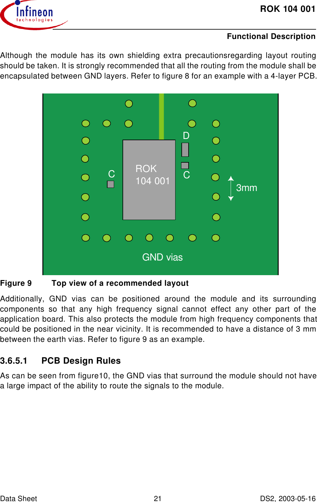
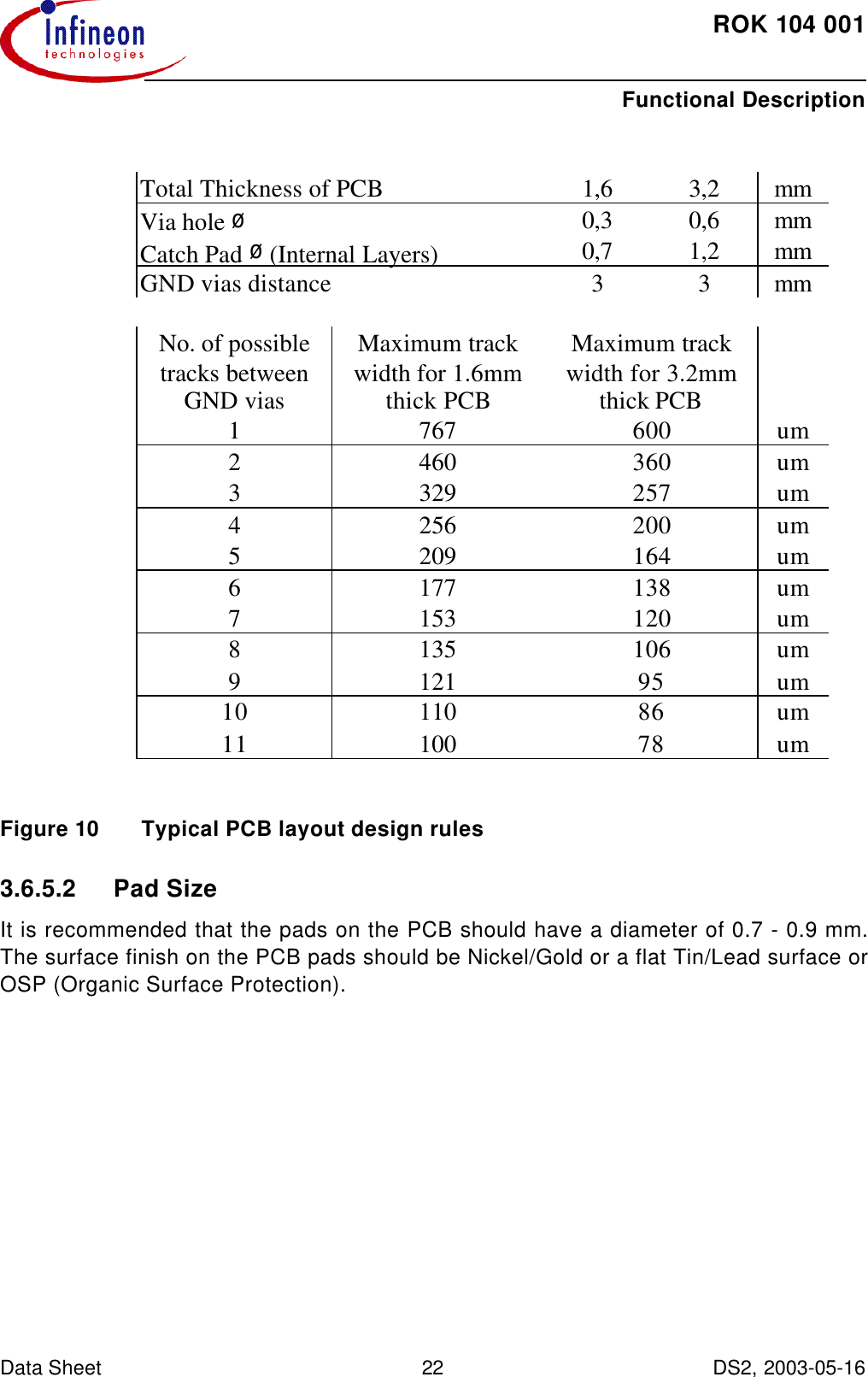
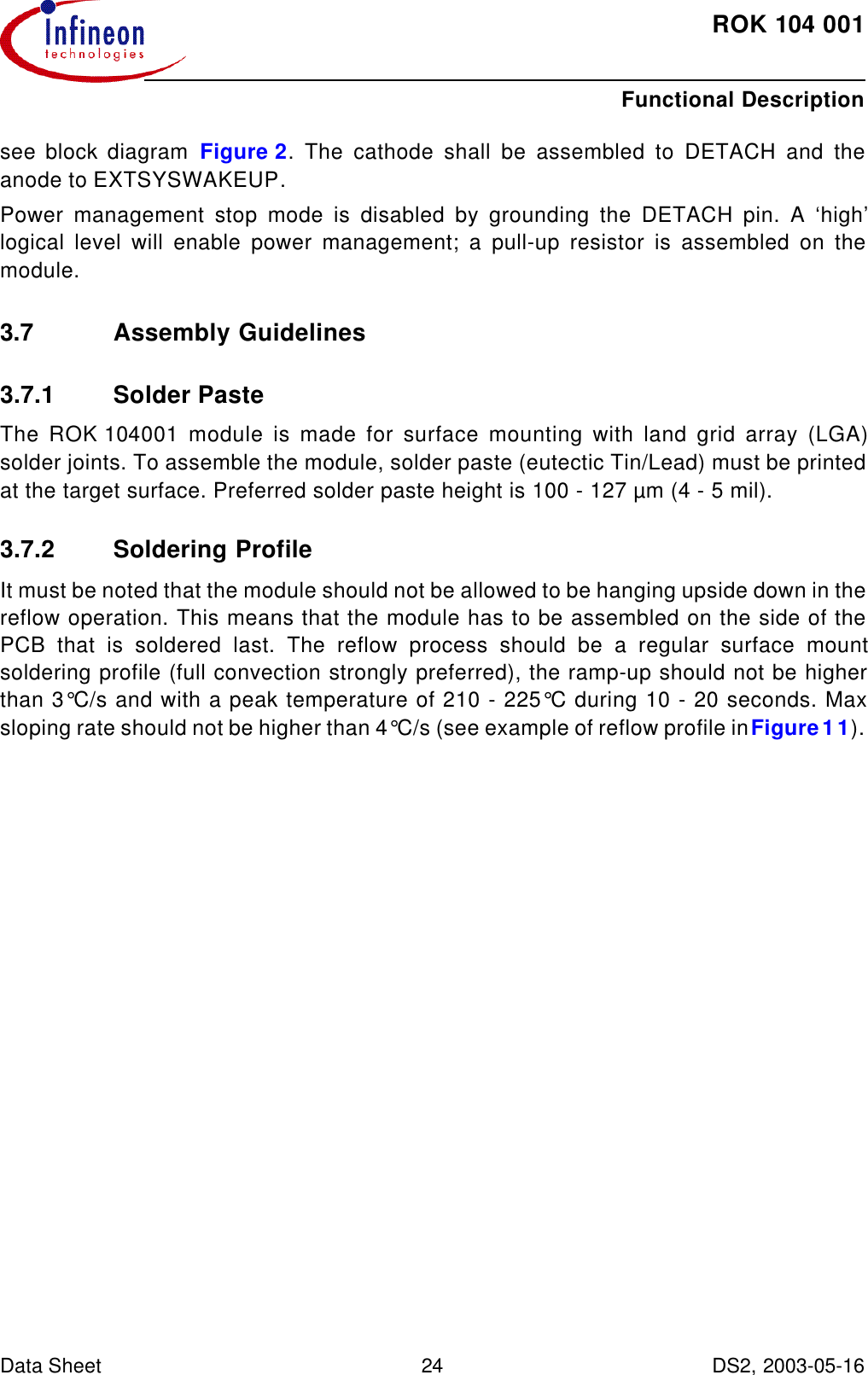
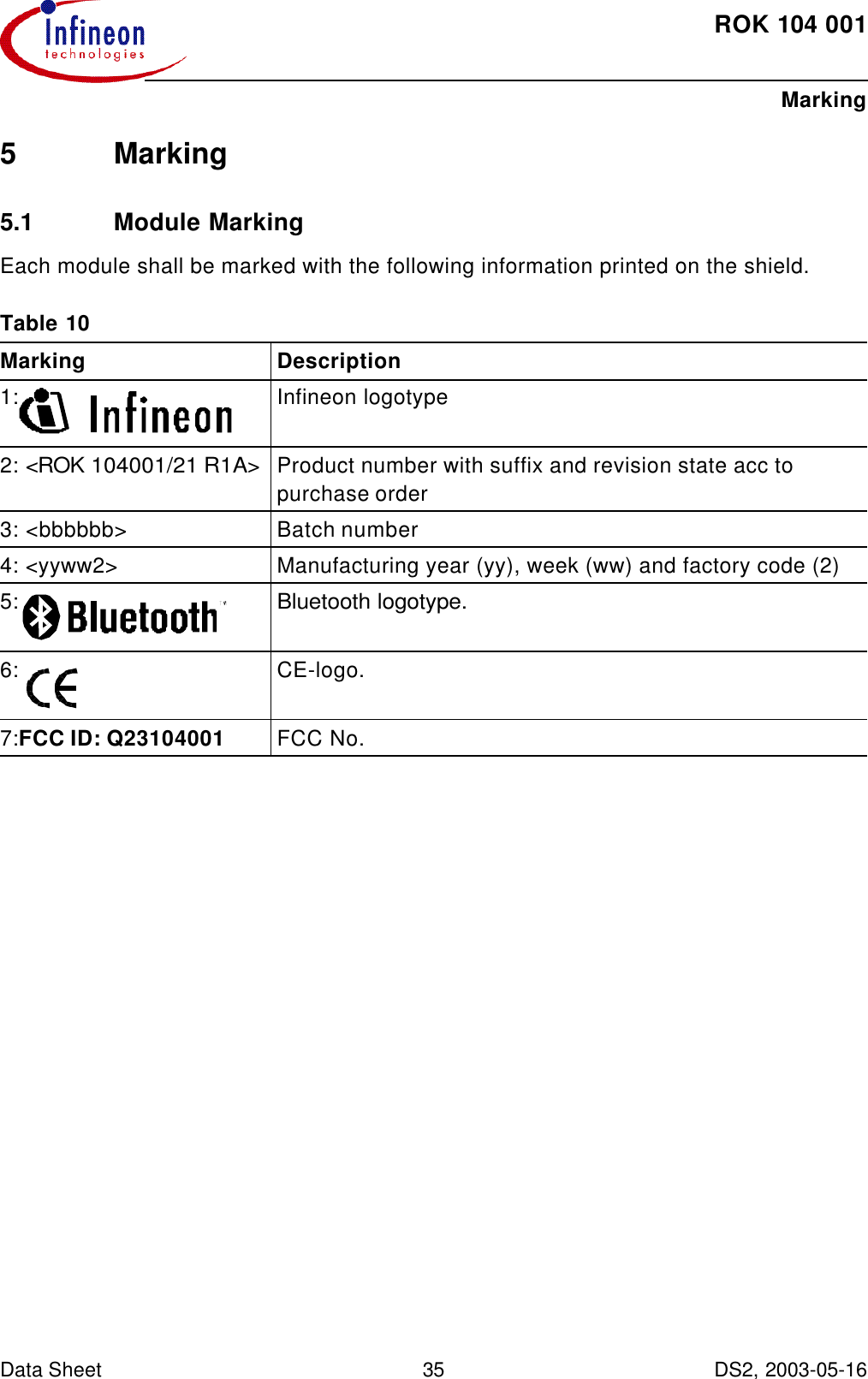
![ROK104001Functional Description Data Sheet 23 DS2, 2003-05-16 3.6.5.3 Spurious Emissions Measurement3.6.6 GroundGround should be distributed with very low impedance as a ground plane. Connect allGND pins to the ground plane.3.6.7 Additional DecouplingA capacitor whose capacitance of 2.2 µF is required between the VDD_RFDIG output andground, see block diagram Figure2. This capacitor must be located as close as possibleto the VDD_RFDIG pad and returned to a clean analogue ground. Any good quality ceramic,tantalum, or film capacitor may be used at the input.3.6.8 Power Management Stop ModeNote that from revision R2C of HCI-firmware and from R3B-revision of ECP-firmware,the Power Management stop mode is disabled by default. In order to enable thisfunction, the 'HCI Command Store In Flash' has to be used (User ID: 131& Flash Data:0001). In order to utilize the power management stop mode features in the firmware; a schottkydiode must be assembled between the DETACH pad and the EXTSYSWAKEUP pad,-80-75-70-65-60-55-50-45Level [dBm]1G 2G 3G 4G 5G 6G 7GFrequency [Hz]MES VLB030214-9_pre PKLIM EN 300328 RX 1-12G Peak Limit (dBm)LIM EN 300328 RX 1-12G2 Limit_2=(Peak Limit)-6 (dBm)](https://usermanual.wiki/Intel-Mobile-Communications/104001/User-Guide-333214-Page-23.png)