Intel Mobile Communications 104001 Wireless Bluetooth module User Manual rok104001 ds a7 v55 rok104001 ds a7 v55
Intel Mobile Communications GmbH Wireless Bluetooth module rok104001 ds a7 v55 rok104001 ds a7 v55
Users Manual

Never stop thinking.
Data Sheet, DS3, June, 2003
Wireless Solutions
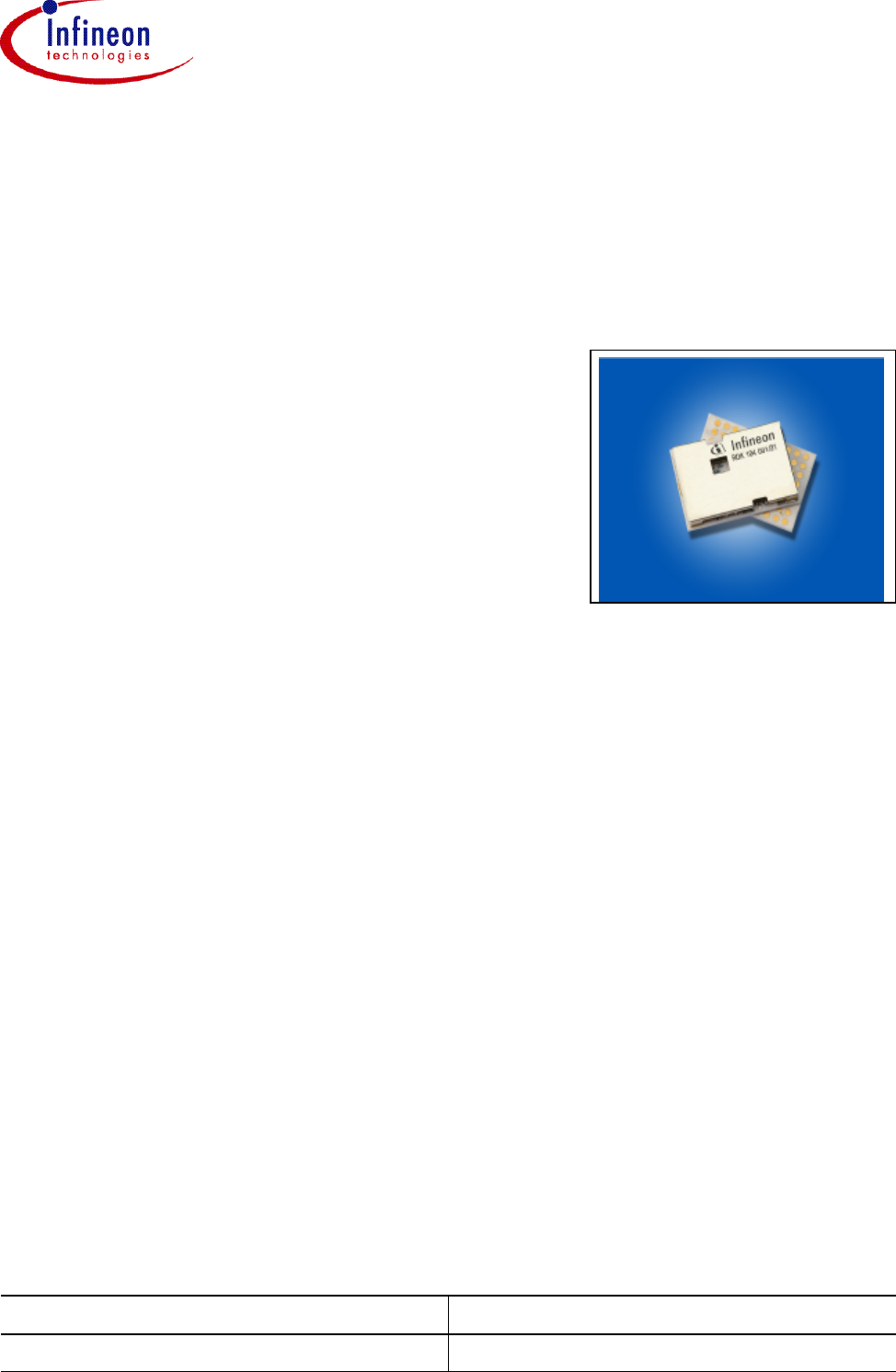
ROK104001
BluetoothTM System Module

Edition 2003-06-16
Published by Infineon Technologies AG,
St.-Martin-Strasse 53,
81669 München, Germany
© Infineon Technologies AG 2003.
All Rights Reserved.
Attention please!
The information herein is given to describe certain components and shall not be considered as warranted
characteristics.
Terms of delivery and rights to technical change reserved.
We hereby disclaim any and all warranties, including but not limited to warranties of non-infringement, regarding
circuits, descriptions and charts stated herein.
Infineon Technologies is an approved CECC manufacturer.
Information
For further information on technology, delivery terms and conditions and prices please contact your nearest
Infineon Technologies Office in Germany or our Infineon Technologies Representatives worldwide
(www.infineon.com).
Warnings
Due to technical requirements components may contain dangerous substances. For information on the types in
question please contact your nearest Infineon Technologies Office.
Infineon Technologies Components may only be used in life-support devices or systems with the express written
approval of Infineon Technologies, if a failure of such components can reasonably be expected to cause the failure
of that life-support device or system, or to affect the safety or effectiveness of that device or system. Life support
devices or systems are intended to be implanted in the human body, or to support and/or maintain and sustain
and/or protect human life. If they fail, it is reasonable to assume that the health of the user or other persons may
be endangered.
For questions on technology, delivery and prices please contact the Infineon
Technologies Offices in Germany or the Infineon Technologies Companies and
Representatives worldwide: see our webpage at http://www.infineon.com.
ROK104001
Revision History: 2003-06-16 DS3
Previous Version: 2003-05-16 DS2
Page Subjects (major changes since last revision)
Updated Information on FCC and R&TTE Approval,
Updated section 3.6.8 on Power Management 2003-June
Document has been updated: 2003-May
Document’s layout has been changed: 2003-Feb.

ROK104001
Data Sheet 3DS1, 2003-02-01
1Overview . . . . . . . . . . . . . . . . . . . . . . . . . . . . . . . . . . . . . . . . . . . . . . . . . . . 5
1.1 Key Features . . . . . . . . . . . . . . . . . . . . . . . . . . . . . . . . . . . . . . . . . . . . . . . . 6
1.2 Reference documents for ECP firmware . . . . . . . . . . . . . . . . . . . . . . . . . . . 6
2Pin Description . . . . . . . . . . . . . . . . . . . . . . . . . . . . . . . . . . . . . . . . . . . . . 7
2.1 Pin Configuration . . . . . . . . . . . . . . . . . . . . . . . . . . . . . . . . . . . . . . . . . . . . . 7
2.2 Pin Definition and Function . . . . . . . . . . . . . . . . . . . . . . . . . . . . . . . . . . . . . 8
3Functional Description . . . . . . . . . . . . . . . . . . . . . . . . . . . . . . . . . . . . . . 11
3.1 Functional Block Diagram . . . . . . . . . . . . . . . . . . . . . . . . . . . . . . . . . . . . . 11
3.2 Design Sections . . . . . . . . . . . . . . . . . . . . . . . . . . . . . . . . . . . . . . . . . . . . . 12
3.2.1 Radio . . . . . . . . . . . . . . . . . . . . . . . . . . . . . . . . . . . . . . . . . . . . . . . . . . . 12
3.2.2 Baseband . . . . . . . . . . . . . . . . . . . . . . . . . . . . . . . . . . . . . . . . . . . . . . . . 12
3.2.3 Voltage Regulation Section . . . . . . . . . . . . . . . . . . . . . . . . . . . . . . . . . . 12
3.2.4 Crystal Oscillator . . . . . . . . . . . . . . . . . . . . . . . . . . . . . . . . . . . . . . . . . . 13
3.2.5 Flash Memory . . . . . . . . . . . . . . . . . . . . . . . . . . . . . . . . . . . . . . . . . . . . 13
3.3 Module HW Interfaces . . . . . . . . . . . . . . . . . . . . . . . . . . . . . . . . . . . . . . . . 13
3.3.1 Host Interfaces . . . . . . . . . . . . . . . . . . . . . . . . . . . . . . . . . . . . . . . . . . . . 13
3.3.1.1 UARTs . . . . . . . . . . . . . . . . . . . . . . . . . . . . . . . . . . . . . . . . . . . . . . . . 13
3.4 Other Interfaces . . . . . . . . . . . . . . . . . . . . . . . . . . . . . . . . . . . . . . . . . . . . . 14
3.4.1 Serial Interface . . . . . . . . . . . . . . . . . . . . . . . . . . . . . . . . . . . . . . . . . . . . 14
3.4.2 General Purpose I/O . . . . . . . . . . . . . . . . . . . . . . . . . . . . . . . . . . . . . . . 14
3.4.3 PCM Voice Interface . . . . . . . . . . . . . . . . . . . . . . . . . . . . . . . . . . . . . . . 14
3.4.4 Antenna . . . . . . . . . . . . . . . . . . . . . . . . . . . . . . . . . . . . . . . . . . . . . . . . . 16
3.5 Software . . . . . . . . . . . . . . . . . . . . . . . . . . . . . . . . . . . . . . . . . . . . . . . . . . . 16
3.5.1 Firmware . . . . . . . . . . . . . . . . . . . . . . . . . . . . . . . . . . . . . . . . . . . . . . . . 16
3.5.2 Bluetooth Module Stack . . . . . . . . . . . . . . . . . . . . . . . . . . . . . . . . . . . . . 17
3.5.3 LM & HCI Firmware . . . . . . . . . . . . . . . . . . . . . . . . . . . . . . . . . . . . . . . . 17
3.5.4 Host Controller Interface (HCI) . . . . . . . . . . . . . . . . . . . . . . . . . . . . . . . 17
3.5.5 Link Manager (LM) . . . . . . . . . . . . . . . . . . . . . . . . . . . . . . . . . . . . . . . . . 18
3.6 Design Guidelines . . . . . . . . . . . . . . . . . . . . . . . . . . . . . . . . . . . . . . . . . . . 19
3.6.1 Power-up Sequence . . . . . . . . . . . . . . . . . . . . . . . . . . . . . . . . . . . . . . . 19
3.6.2 RESET . . . . . . . . . . . . . . . . . . . . . . . . . . . . . . . . . . . . . . . . . . . . . . . . . . 19
3.6.3 Power . . . . . . . . . . . . . . . . . . . . . . . . . . . . . . . . . . . . . . . . . . . . . . . . . . . 19
3.6.4 Antenna . . . . . . . . . . . . . . . . . . . . . . . . . . . . . . . . . . . . . . . . . . . . . . . . . 20
3.6.5 Shielding / EMC Requirements . . . . . . . . . . . . . . . . . . . . . . . . . . . . . . . 20
3.6.5.1 PCB Design Rules . . . . . . . . . . . . . . . . . . . . . . . . . . . . . . . . . . . . . . . 21
3.6.5.2 Pad Size . . . . . . . . . . . . . . . . . . . . . . . . . . . . . . . . . . . . . . . . . . . . . . 22
3.6.5.3 Spurious Emissions Measurement . . . . . . . . . . . . . . . . . . . . . . . . . . 23
3.6.6 Ground . . . . . . . . . . . . . . . . . . . . . . . . . . . . . . . . . . . . . . . . . . . . . . . . . . 23
3.6.7 Additional Decoupling . . . . . . . . . . . . . . . . . . . . . . . . . . . . . . . . . . . . . . 23
3.6.8 Power Management Stop Mode . . . . . . . . . . . . . . . . . . . . . . . . . . . . . . 23
3.7 Assembly Guidelines . . . . . . . . . . . . . . . . . . . . . . . . . . . . . . . . . . . . . . . . . 24
3.7.1 Solder Paste . . . . . . . . . . . . . . . . . . . . . . . . . . . . . . . . . . . . . . . . . . . . . 24

ROK104001
Data Sheet 4DS1, 2003-02-01
3.7.2 Soldering Profile . . . . . . . . . . . . . . . . . . . . . . . . . . . . . . . . . . . . . . . . . . 24
3.7.3 Placement . . . . . . . . . . . . . . . . . . . . . . . . . . . . . . . . . . . . . . . . . . . . . . . 25
3.7.4 Storage . . . . . . . . . . . . . . . . . . . . . . . . . . . . . . . . . . . . . . . . . . . . . . . . . 25
3.8 FCC Modular Approval . . . . . . . . . . . . . . . . . . . . . . . . . . . . . . . . . . . . . . . 25
3.9 R&TTE Approval . . . . . . . . . . . . . . . . . . . . . . . . . . . . . . . . . . . . . . . . . . . . 26
4Electrical Characteristics . . . . . . . . . . . . . . . . . . . . . . . . . . . . . . . . . . . . 27
4.1 Absolute Maximum Ratings . . . . . . . . . . . . . . . . . . . . . . . . . . . . . . . . . . . . 27
4.2 DC Specifications . . . . . . . . . . . . . . . . . . . . . . . . . . . . . . . . . . . . . . . . . . . 28
5Marking . . . . . . . . . . . . . . . . . . . . . . . . . . . . . . . . . . . . . . . . . . . . . . . . . . . 35
5.1 Module Marking . . . . . . . . . . . . . . . . . . . . . . . . . . . . . . . . . . . . . . . . . . . . . 35
5.2 Reel Marking . . . . . . . . . . . . . . . . . . . . . . . . . . . . . . . . . . . . . . . . . . . . . . . 36
6Package Outlines . . . . . . . . . . . . . . . . . . . . . . . . . . . . . . . . . . . . . . . . . . . 37
6.1 Pinout (bottom view) . . . . . . . . . . . . . . . . . . . . . . . . . . . . . . . . . . . . . . . . . 38
6.2 Footprint, Land View . . . . . . . . . . . . . . . . . . . . . . . . . . . . . . . . . . . . . . . . . 38
7Ordering Information . . . . . . . . . . . . . . . . . . . . . . . . . . . . . . . . . . . . . . . . 39
8Packaging . . . . . . . . . . . . . . . . . . . . . . . . . . . . . . . . . . . . . . . . . . . . . . . . . 39
9Abbreviations . . . . . . . . . . . . . . . . . . . . . . . . . . . . . . . . . . . . . . . . . . . . . . 39
Type Package
ROK104001 LGA-87
BluetoothTM System Module ROK104001
Preliminary Data
Data Sheet 5DS2, 2003-05-16
1Overview
The Bluetooth 1.1 System Module ROK104001 is a
complete FCC and R&TTE type approved product for
fast implementation and cuts your time-to-market. It is a
compact and cost effective radio/baseband module that
can be implemented in any kind of electronic device. The
module includes a baseband processor with 4Mbit Flash
memory, a radio solution, interfaces to antenna and
application, supporting circuitry, together with basic
Bluetooth software for signaling at HCI level (Host Controller Interface) or ECP level
(Embedded Communication Platform).
The antenna filter is specially designed for applications in a GSM environment such as
inside a mobile phone. The ROK104001 also has a very high threshold for high signal
levels in-band, which makes it very suitable to be in an IEEE 802.11b environment.
As the ROK104001 is a generic product, it can be used for many different types of
applications that require Bluetooth capability such as
•Computers and peripherals
•Handheld devices and accessories
•Inustrial and medical sensors
•Access points and home base stations
•Applications where short time-to-market is required

ROK104001
Overview
Data Sheet 6DS2, 2003-05-16
1.1 Key Features
•A small and complete class 2 Bluetooth system
•Forms full Bluetooth functionality with only the addition of an antenna
•Point to multipoint, 7 slaves for HCI firmware and 3 slaves for ECP firmware
•Power management: PARK, SNIFF & HOLD as well as system power saving
•Excellent high signal level performance in-band
•Exceptional out-band blocking in all GSM bands
•Multiple interfaces UART, PCM, bi-directional serial interface/GPIO
•Capability of embedded solutions
•Qualified to Bluetooth spec. 1.1
•FCC and R&TTE type approved
•Supports all Bluetooth profiles
1.2 Reference documents for ECP firmware
•ECI Protocol Specification
•ECI Driver User Manual
•ECI Driver Release Notes
•ECI Firmware Release Notes
These documents can be provided through your Infineon Technologies sales contact.
ROK104001
Pin Description
Data Sheet 7DS2, 2003-05-16
2Pin Description
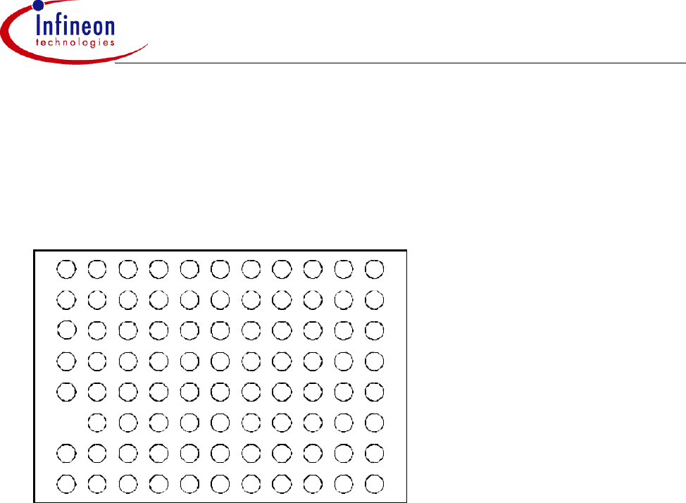
2.1 Pin Configuration
Figure1 ROK104001, Bottom View
ERA00099
VTRPNMLKJHG
0
1
2
3
4
5
6
7

ROK104001
Pin Description
Data Sheet 8DS2, 2003-05-16
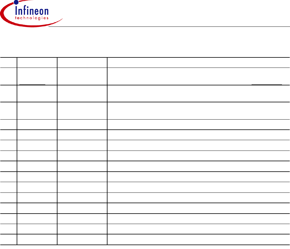
2.2 Pin Definition and Function
Table1 Pin Definition and Function
Pin Symbol Type 1) Description
G0-2 GND Power Mechanical connection to ground
G3-4 N.C. Mechanical connection - treat as no connect. Pad required.
G5-7 GND Power Mechanical connection to ground
H0 N.C. Mechanical connection - treat as no connect. Pad required.
H1 GND Power Mechanical connection to ground
H2 D- BD, PHY, IOP2 USB data pin (USB function is not supported)
H3 D+ BD, PHY, IOP2 USB data pin (USB function is not supported)
H4 ON DI, Power When tied to VDD, the module is HW enabled
H5 GND Power Ground
H6 GND Power Mechanical connection to ground
H7 N.C. Mechanical connection - treat as no connect. Pad required.
J0 N.C. Mechanical connection - treat as no connect. Pad required.
J1 UART2Tx DO, IOP1 Tx data from UART 2 - not supported by HCI FW
J2 UART2CTS DIU, IOP1 Flow control signal, Clear To Send data to UART 2 - not supported by
HCI FW
J3 UART1CTS DIU, IOP2 Flow control signal, Clear To Send data to UART 1
J4 VDDIO Power External supply rail to the input / output ports
J5 VDD Power Supply Voltage
J6 GND Power Ground
J7 N.C. Mechanical connection - treat as no connect. Pad required.
K0 N.C. Mechanical connection - treat as no connect. Pad required.
K1-2 N.C. Not connected
K3 UART1RTS DO, IOP2 Flow control signal, Request To Send data from UART 1
K4 UART1Tx DO, IOP2 Tx data from UART 1
K5 N.C. Not connected
K6 GND Power Signal ground
K7 N.C. Mechanical connection - treat as no connect. Pad required.
L0 N.C. Mechanical connection - treat as no connect. Pad required.
L1 PCMRx BDU, IOP2 (input
default) PCM receive data (default)
L2 PCMSYNC BD, IOP2 PCM data sampling rate
L3 WAKEUP DO, IOP2 Indicates that the module wants to be attached (USB function is not
supported)
L4 GND Power Ground
L5 N.C. Not connected

ROK104001
Pin Description
Data Sheet 9DS2, 2003-05-16
L6 GND Power Ground
L7 N.C. Mechanical connection - treat as no connect. Pad required.
M0 GND Power Mechanical connection to ground
M1 PCMCLK BD, IOP2 PCM clock that sets the PCM data rate
M2 EXTINT DID, IOP1 External interrupt for embedded purposes
M3 UART1Rx DIU, IOP2 Receive data to UART 1
M4 N.C. Not connected
M5 PWRAVAIL DID, IOP1 Indicates whether external power is available; used in conjunction
with PWRFAIL - not supported by HCI FW
M6 N.C. - VTP4 DO Not connected - vendor test point #4
M7 GND Power Mechanical connection to ground
N0 N.C. Mechanical connection - do not connect
N1 PCMTx BD, IOP2 (output
default) PCM transmit data (default)
N2 UART2Rx DIU, IOP1 Receive data to UART 2 - not supported by HCI FW
N3 GPIOB5 BD, IOP2 General purpose signal #5 input / default output for embedded
purposes
N4 GPIOB4 BD, IOP1 General purpose signal #4 input / default output for embedded
purposes
N5 UART2RTS DO, IOP1 Flow control signal, Request To Send data from UART 2 - not
supported by HCI FW
N6 N.C. - VTP3 DI Not connected -vendor test point #3
N7 VDD-RFDIG AO Output from internal regulator connected to digital section of the radio.
Shall be connected to a minimum capacitance of 2.2µF.
P0 N.C. Mechanical connection - treat as no connect. Pad required.
P1 GPIOB3 BD, IOP1 General purpose signal #3 input / default output for embedded
purposes
P2 EXTSYS
WAKEUP DI, IOP1 Can be used as an external interrupt to control the EBC - for
embedded purposes
P3 SERIALCLK BD3, IOP1 Bidirectional serial interface / GPIO clock signal
P4 DETACH DIU, IOP2 Indicates that the USB host wants to detach the module (USB function
is not supported)
P5 N.C. - VTP2 DO Not connected - vendor test point #2
P6 GPIOB6 BD, IOP1 General purpose signal #6 input / default output for embedded
purposes
P7 N.C. Mechanical connection - treat as no connect. Pad required.
R0 N.C. - VTP5 AO
Not connected - vendor test point (VDD_DIG) #5
R1-2 GND Power Ground
R3 RESET DI, IOP1 Reset signal, active low (must be fed from an open drain output)
Table1 Pin Definition and Function (cont’d)
Pin Symbol Type 1) Description
ROK104001
Pin Description
Data Sheet 10 DS2, 2003-05-16
R4 GPIOB2 BD, IOP1 General purpose signal #2 input / default output for embedded
purposes
R5 PWRFAIL DIU, IOP1 Indicates a poer fail condition; used in conjunction with PWRAVAIL -
not supported by HCI FW
R6 GPIOB7 BD, IOP1 General purpose signal #7 input / default output for embedded
purposes
R7 N.C. Mechanical connection - treat as no connect. Pad required.
T0 N.C. Mechanical connection - treat as no connect. Pad required.
T1 GND Power Ground
T2 ANT BD, RF 50 Ω antenna connection
T3 GND Power Ground
T4 N.C. Not connected
T5 N.C. - VTP1
Not connected - vendor test point #1
T6
SERIALDATA
BD, IOP1 Serial interface - data signal
T7 N.C. Mechanical connection - treat as no connect. Pad required.
V0-1 GND Power Mechanical connection to ground
(V2) (No pad)
V3-7 GND Power Mechanical connection to ground
1) AO = Analogue output pad
BD = Bi-directional pad
BDU = Bi-directional pad with pull-up
DI = Input pad
DIU = Input pad with pull-up
DID = Input pad with pull-down
DO = Digital Output
GND = VSS power supply pad
IOP1 = IO group VDD_DIG power supply pad
IOP2 = IO group VDD_IO power supply pad
POW = Core power supply pad
PHY = USB transceiver pad shared with UART1 RI and DCD pins (USB function is not supported)
RF = Radio Frequency pad
Table1 Pin Definition and Function (cont’d)
Pin Symbol Type 1) Description
ROK104001
Functional Description
Data Sheet 11 DS2, 2003-05-16
3Functional Description
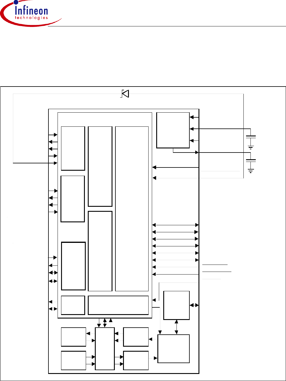
3.1 Functional Block Diagram
Figure2 Block Diagram
The ROK104001 is a complete Bluetooth module that has been specified and designed
according to the Bluetooth System v1.1. Its implementation is based on a high-
UART1
UART2
PCM
Serial
Interface
Flash
Memory
EBC
(ARM7)
Embedded
Control
Radio Control
PBM 990 80
Voltage
Regulation
Antenna
Filter
Ra dio
ASIC
Loop
Filter
13 MHz
Crystal
Rx-
Balun
Tx-
Balun
Antenna
Switch
UART1RxD
UART1TxD
UART1RTS
UART1CTS
UART2RxD
UART2TxD
UART2RTS
UART2CTS
PCMRx
PCMTx
PCMCLK
PCMSYNC
SERIALCLK
SERIALDATA
ON
VDD
VDDIO
VDD _RFDIG
EXTINT
EXTSYSWAKEUP
GPIOB2
GPIOB3
GPIOB4
GPIOB5
GPIOB6
GPIOB7
PWRFAIL
PWRAVAIL
RESET
ANT
>1µF
2.2µF
Shall be
positioned
as close
as possible
tomodule.
Only required forPMstop mode function
DETACH

ROK104001
Functional Description
Data Sheet 12 DS2, 2003-05-16
performance integrated radio IC working with the baseband controller PBM 990 80, with
integrated flash memory and surrounding secondary components.
ROK104001 consists of three major parts; a baseband controller, firmware, and a radio.
Multi slot data and voice packets are supported. Communication between the module
and the host controller is carried out on UART and PCM interfaces. ROK104001 is
compliant with BT version 1.1 and is a Class 2 BT Module. ROK 104 001 is tested
according to R&TTE and FCC type approval requirements.
3.2 Design Sections
ROK104001 has five major design sections. Figure 2 illustrates the interaction of the
various sections. The functionality of each section will be briefly explained.
3.2.1 Radio
The radio functionality is achieved by an Infineon Technologies Radio IC, a short-range
microwave frequency radio transceiver for Bluetooth communication links based on
RFCMOS technology.
3.2.2 Baseband
The baseband functionality is achieved by using Infineon Technologies PBM 990 80,
providing the baseband functionality and Flash memory. The baseband contains a
Bluetooth core (EBC); an ARM 7 processor, I/O ports (PCM and UART) and RAM
memory. Firmware is downloaded into the flash memory. The interfaces that are
implemented on the baseband chip are UART, PCM and serial clock interface (bi-
directional serial interface / GPIO).
PBM99080 provides the link-setup and control routines for the layers above.
Furthermore, PBM99080 also provides Bluetooth security like encryption,
authentication and key management.
Please refer to the PBM99080 data sheet for further information regarding baseband
functionallity.
3.2.3 Voltage Regulation Section
There are three inputs to the voltage regulation section (VDD, VDD_IO, ON). VDD can be
fed with 3.1V to 4.75V. The power regulator on the module creates 2.7 V regulated
supply.
A separate power supply rail (
VDD_IO) is provided for the I/O ports, UART and PCM.
VDD_IO can either be connected to VDD or to a dedicated supply rail, which is the same as
the logical interface of the host.
The ON input is the only signal that is required to activate the module.

ROK104001
Functional Description
Data Sheet 13 DS2, 2003-05-16
3.2.4 Crystal Oscillator
An internal crystal oscillator supplies radio IC and Baseband with a stable frequency. No
external oscillator or crystal is required.
3.2.5 Flash Memory
ROK104001 is delivered with 4Mbit Flash memory. Firmware (F/W), in terms of link
manager and applicable upper layer stack parts, resides in the Flash and is available as
image file formats.
3.3 Module HW Interfaces
3.3.1 Host Interfaces
To enable a host system to access the Bluetooth radio link, a Host Controller Interface
(HCI) has been defined. The host system controls and distributes data to and from the
Bluetooth Link Manager with a set of commands. These commands are carried
physically on either the UART or USB interface (not supported by firmware).
3.3.1.1 UARTs
The UART implemented on the baseband is an industry standard and supports the
following baud rates: 300, 600, 900, 1200, 1800, 2400, 4800, 9600, 19200, 38400,
57600, 115200, 230400, 460800 and 921600 bits/s. 128-byte FIFOs are associated with
the UART1.
Four signals will be provided for the UART interface. TxD & RxD are used for data flow,
and RTS & CTS shall be used for flow control. The module is a DCE.
There are two on-chip UART interfaces, UART1 and UART2.
UART1 has 128-byte FIFOs and full modem control support and is used for data in and
out transmission at bit rates up to 921 kbit/s. UART1 is setup to a DTE configuration.
UART2 has 16-byte FIFOs and is used for control and/or boot.
Start-detect and Auto-baud functionality is available for both UARTs.

ROK104001
Functional Description
Data Sheet 14 DS2, 2003-05-16
Note: These settings can be changed from the HCI level using Ericsson specific
commands. For HCI and ECP firmware, UART2 is disabled since UART1 is
default.
3.4 Other Interfaces
3.4.1 Serial Interface
The bi-directional serial interface / GPIO interface function is based on software using
two GPIO’s. The interface has a capacity of handling approximately 100 kbit/s.
A master serial I/F is available on the module. This is used to control external serial
interface devices. The controls of the serial interface pins are performed by Ericsson
specific HCI commands available in the FW implementation. See Application Note. This
enables application in a stand-alone ROK 104 001 module to also control other devices
via the serial interface.
3.4.2 General Purpose I/O
The ROK104001 architecture supports up to 8 General Purpose I/O’s. 2 GPIO’s are
default, that is used as the serial interface.
3.4.3 PCM Voice Interface
Uses the standard PCM interface, which has a sample rate of 8 kHz (PCMSYNC). The
PCM I/F can be set in master or slave mode (providing or receiving the PCMSYNC and
PCMCLK).
PCM clock (PCMCLK) is variable between 200kHz and 2.048 MHz in slave mode.
During the master mode, the PCMCLK is set at 2 MHz. PCM data can be linear PCM
(13-16bit), µ-Law (8 bit) or A-Law (8 bit).
Over the air the encoding is programmable to be CVSD, A-Law or µ-Law.
Table2 HCI Default Settings UART1, UART2
Speed 57600 bit/s
Data bit 8 bit
Stop bit One
Parity None
Flow CTS/RTS
ROK104001
Functional Description
Data Sheet 15 DS2, 2003-05-16
The PCM line interface can act either as slave or master. When the PCM line interface
is slave the frequency range of PCMCLK (in) is 200 kHz to 2.048 MHz. When the PCM
line interface is master PCMCLK (out) is always 2 MHz.
Each PCM symbol on the PCMTx or PCMRx line is organized as an 8 or 16-bit sequence
of bits, arriving synchronous to PCMCLK in (if the PCM line interface is slave) or
PCMCLK out (if the PCM line interface is master). The symbol starts with its most
significant bit arriving after a positive edge on the PCMCLK in (or out), one clock cycle
after a PCMSYNC in (or out) positive transition. The symbol is then transferred by one
bit each PCMCLK in (or out) clock cycle until the least significant bit is transferred. The
EBC then samples the arriving bit at falling edges of PCMCLK in (or out).
The PCM symbols are transmitted bit by bit starting with the MSB, one clock cycle after
a positive edge on the PCMCLK in (if the PCM line interface is slave) or PCMCLK out (if
the PCM line interface is master), one clock cycle after a PCMSYNC (in or out) positive
transition. The rest of the bits are then transferred by one bit each PCMCLK (in or out)
cycle, and are synchronized with the rising edge of this clock.
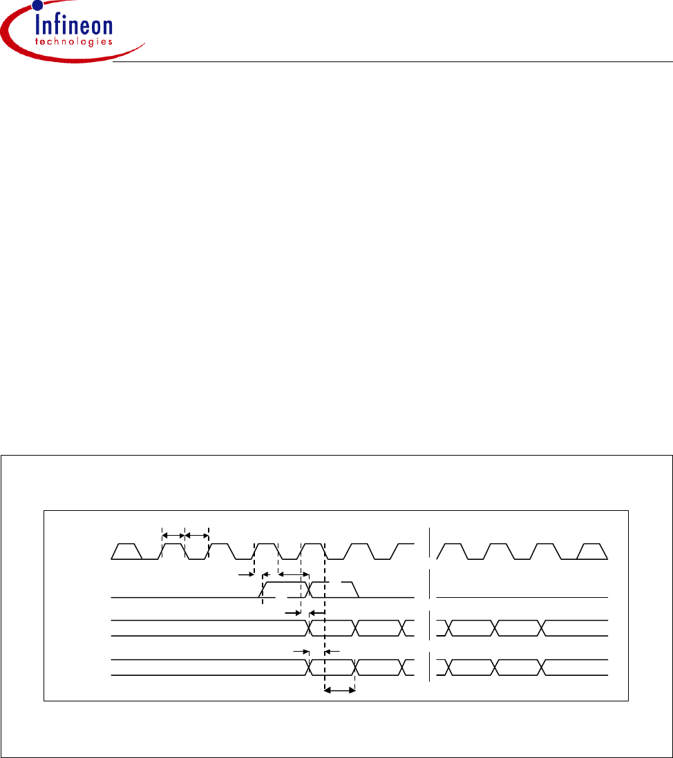
Figure3 PCM Master Mode Timing Diagram
ZZ
0,1 orZ0,1 orZ
tPCH Continuous
PCMclock
Continuous
PCMclock
Delayed PCMsync
PCMSYNC out
PCMCLKout
PCMXin
PCMXout
tPDIH
tPDIS
tPDOV
tPSH
tPSV
tPCL
MSB MSB-1D1D0
D1D0MSB MSB-1
ROK104001
Functional Description
Data Sheet 16 DS2, 2003-05-16
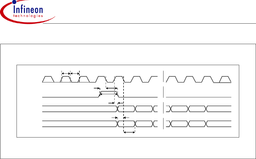
Figure4 PCM Slave Mode Timing Diagram
3.4.4 Antenna
The ANT pin should be connected to a 50 Ω antenna interface, thereby supporting the
best signal strength performance, VSWR should not be higher than 2:1. Infineon
Technologies can recommend application specific antennas.
3.5 Software
The Bluetooth link is partitioned into a hardware part and a software part. The software
relates to the Bluetooth protocol stack. Depending on the level of integration, there will
be two different firmware models available, including hardware specific drivers for the
Bluetooth core, UARTs, GPIO and bidirectional serial interface / GPIO. The level of
integration follows the two main scenarios:
•LM & HCI firmware for HCI based applications, where the upper layer stack is
integrated in a host processor external to the ROK104001
•Embedded Communication Platform (ECP) where LM and upper layer Bluetooth
stack resides in the ROK 104001, communicating with an external host processor
through an easy to use ECI-interface (Embedded Communication Interface). For
further documentation on ECP and ECI, please refer to ECI-driver documentation.
3.5.1 Firmware
The module includes firmware for the host controller interface, HCI, and the link
manager, LM. The FW resides in the Flash and is available in load format (*.mfl) and in
binary format (*.bin).
0,1 orZ
Z Z
0,1 orZ
tPCH
Continuous
PCMclock
tPSW
tPSS
Continuous
PCMclock
PCMSYNC in
PCMCLKin
PCMXin
PCMXout
tPDIH
tPDIS
tPDOV
tPSH
tPCL
MSB MSB-1D1D0
D1D0MSB MSB-1
ROK104001
Functional Description
Data Sheet 17 DS2, 2003-05-16
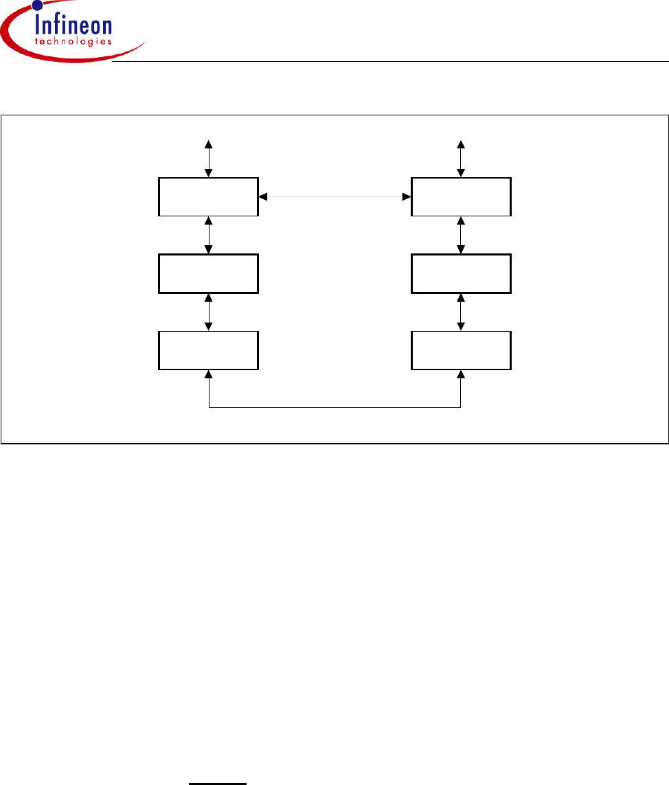
3.5.2 Bluetooth Module Stack
The Host Controller Interface (HCI) handles the communication by the transport layer
through the UART interface with the host. The Baseband and radio provide a secure and
reliable radio link for higher layers. The following sections describe the Bluetooth module
stack in more detail, see also Figure5. It is implemented in accordance with and
complies with the Specification of the Bluetooth System v1.1.
Figure5 HW/HCI FW Parts Included in the Bluetooth Module from Infineon
3.5.3 LM & HCI Firmware
In this configuration the customer will access the LM through a Host Controller Interface
(HCI) protocol distributed over UART.
3.5.4 Host Controller Interface (HCI)
The HCI provides a uniform command I/F to the Baseband and Link Manager and also
to HW status registers. The HCI I/F is accessed through UART. There are three different
types of HCI packets:
•HCI command packet - from host to Bluetooth module HCI
•HCI event packets - from Bluetooth module HCI to host
•HCI data packets - going both ways
It is not necessary to make use of all different commands and events for an application.
If the application is aimed at a pre-specified profile, the capabilities of such a profile are
necessary to adjust to - see Specification of the Bluetooth System v1.1. Profiles and
Application Note
a) With the HCI UART Transport Layer on top of HCI, the module will communicate with
a host through the UART I/F. The PCM I/F is also available for communicating voice.
Please refer to the Specification of the Bluetooth System v1.1 part H: 1-4 for in-depth
information regarding the HCI and different transport layers.
ERA00103
Audio
HCI
Link Manager
Baseband
Radio
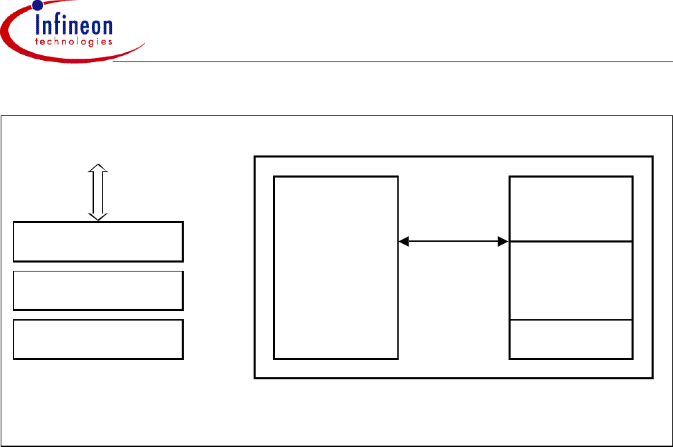
ROK104001
Functional Description
Data Sheet 18 DS2, 2003-05-16
Figure6 Host Controller Interface
3.5.5 Link Manager (LM)
The Link Manager in each Bluetooth module can communicate with another Link
Manager by using the Link Manager Protocol (LMP) which is a peer to peer protocol, see
Figure7. The LMP messages have the highest priority and are used for link-setup,
security, control and power saving modes. The receiving Link Manager filters out the
message and does not need to acknowledge the message to the transmitting LM due to
the reliable link provided by the Baseband and radio. LM to LM communication can take
place without actions taken by the host. Discovery of features at other Bluetooth enabled
devices nearby can be found and saved for later use by the host. Please refer to the
Specification of the Bluetooth System v1.1 part C for in-depth information regarding the LMP.
ERA00104
PBM 990 80
LM
HCI
UARTPBM 990 80
Running:
•LM
•HCI
OS:OSE
UART
Running:
•Host Stack
•Application
OS:Customer
Host System
Controller
ROK104001
Functional Description
Data Sheet 19 DS2, 2003-05-16
Figure7 Link Manager
3.6 Design Guidelines
3.6.1 Power-up Sequence
There is no need for a power up sequence if VDD, ON and VDD_IO are tied together. A
power up sequence, if used, shall be applied accordingly: GND, VDD_IO supply rail, VDD
supply; and finally the ON signal should be applied in order to initiate the internal
regulator.
The power-down sequence is similar to the power-up procedure but in the reverse
format. Therefore, the disconnection of the signals shall be as follows: ON, VDD, VDD_IO,
and finally GND.
3.6.2 RESET
The assignment of the RESET input is to generate a reset signal to ROK104001.
During power-up the reset signal is set ‘low’ so that power supply glitches are avoided.
Therefore, no reset input is required after power-up.
3.6.3 Power
There are three inputs to the Voltage Management section (VDD, VDD_IO, ON). VDD is the
supply voltage that is typically 3.3 V.
A separate power supply rail (
VDD_IO) is provided for the I/O ports, UART and PCM.
VDD_IO can either be connected to VDD or to a dedicated supply rail, which is the same as
the logical interface of the host.
The ON signal is controlling the internal regulators on or off.
ERA00105
LM
LC
RF
LM
LC
RF
Physical layer
LMP

ROK104001
Functional Description
Data Sheet 20 DS2, 2003-05-16
An input capacitor whose capacitance is > 1 µF is required between the VDD supply and
ground (the amount of capacitance may be increased without limit), see Figure2. This
capacitor must be located as close as possible to the VDD pad returned to a clean
analogue ground. Any good quality ceramic, tantalum, or film capacitor may be used at
the input.
Important: Tantalum capacitors can suffer catastrophic failure due to surge current when
connected to a low-impedance source of power (like a battery or very large capacitor). If
a Tantalum capacitor is used at the input, it must be guaranteed by the manufacturer to
have a surge current rating sufficient for the application.
There are no requirements for ESR on the input capacitor, but tolerance and
temperature coefficient must be considered when selecting the capacitor to ensure that
the capacitance will be > 1 µF over the entire operating temperature range.
3.6.4 Antenna
The antenna output routing should be 50 Ω (VSWR ≤ 2:1) all the way to the antenna in
order to maintain the radio performance listed in this data sheet. For the routing
underneath the module, the modules ground plane should be considered. The type
approval for FCC and R&TTE have been done with an antenna gain of 1.6dBi.
3.6.5 Shielding / EMC Requirements
The module has its own RF shielding and is approved according to the standards by FCC
and R&TTE. If the approval number is not visible on the outside when the module is
utilised in the final product, an exterior label must state that there is a transmitter module
inside the product (see Section 3.8).
Figure8 Side view of a recommended layout for a 4 layer PCB
ROK 104 001
CC
GND vias GND vias
Route 1/GND
GND
Route 2
GND
ROK104001
Functional Description
Data Sheet 21 DS2, 2003-05-16
Although the module has its own shielding extra precautionsregarding layout routing
should be taken. It is strongly recommended that all the routing from the module shall be
encapsulated between GND layers. Refer to figure 8 for an example with a 4-layer PCB.
Figure9 Top view of a recommended layout
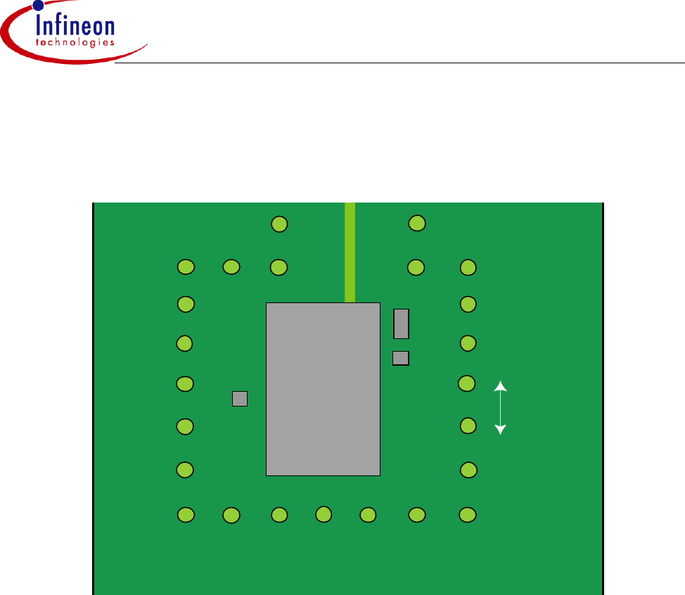
Additionally, GND vias can be positioned around the module and its surrounding
components so that any high frequency signal cannot effect any other part of the
application board. This also protects the module from high frequency components that
could be positioned in the near vicinity. It is recommended to have a distance of 3 mm
between the earth vias. Refer to figure 9 as an example.
3.6.5.1 PCB Design Rules
As can be seen from figure10, the GND vias that surround the module should not have
a large impact of the ability to route the signals to the module.
3mm
ROK
104 001
CC
D
GND vias

ROK104001
Functional Description
Data Sheet 22 DS2, 2003-05-16
Figure10 Typical PCB layout design rules
3.6.5.2 Pad Size
It is recommended that the pads on the PCB should have a diameter of 0.7 - 0.9 mm.
The surface finish on the PCB pads should be Nickel/Gold or a flat Tin/Lead surface or
OSP (Organic Surface Protection).
Total Thickness of PCB 1,6 3,2 mm
Via hole ø0,3 0,6 mm
Catch Pad ø (Internal Layers) 0,7 1,2 mm
GND vias distance 3 3 mm
No. of possible
tracks between
GND vias
Maximum track
width for 1.6mm
thick PCB
Maximum track
width for 3.2mm
thick PCB
1767 600 um
2460 360 um
3329 257 um
4256 200 um
5209 164 um
6177 138 um
7153 120 um
8135 106 um
9121 95 um
10 110 86 um
11 100 78 um
ROK104001
Functional Description
Data Sheet 23 DS2, 2003-05-16
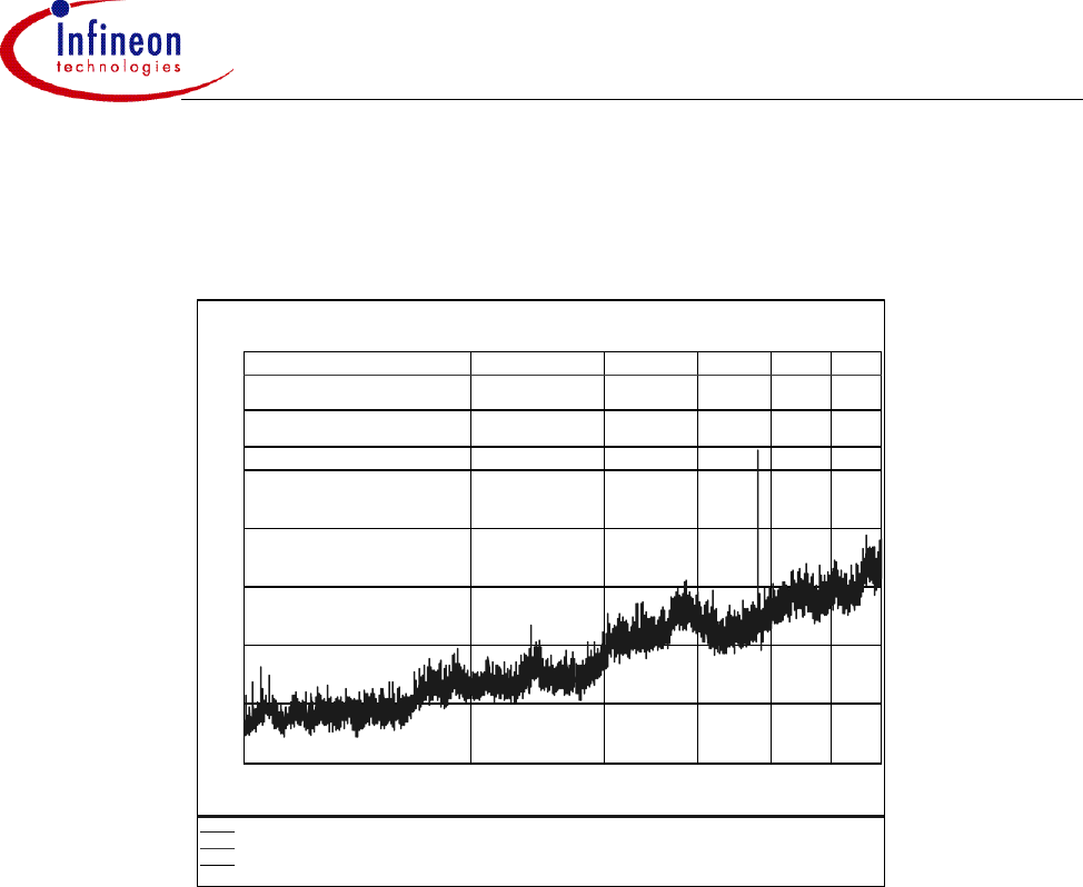
3.6.5.3 Spurious Emissions Measurement
3.6.6 Ground
Ground should be distributed with very low impedance as a ground plane. Connect all
GND pins to the ground plane.
3.6.7 Additional Decoupling
A capacitor whose capacitance of 2.2 µF is required between the VDD_RFDIG output and
ground, see block diagram Figure2. This capacitor must be located as close as possible
to the VDD_RFDIG pad and returned to a clean analogue ground. Any good quality ceramic,
tantalum, or film capacitor may be used at the input.
3.6.8 Power Management Stop Mode
Note that from revision R2C of HCI-firmware and from R3B-revision of ECP-firmware,
the Power Management stop mode is disabled by default. In order to enable this
function, the 'HCI Command Store In Flash' has to be used (User ID: 131& Flash Data:
0001).
In order to utilize the power management stop mode features in the firmware; a schottky
diode must be assembled between the DETACH pad and the EXTSYSWAKEUP pad,
-80
-75
-70
-65
-60
-55
-50
-45
Level [dBm]
1G 2G 3G 4G 5G 6G 7G
Frequency [Hz]
MES VLB030214-9_pre PK
LIM EN 300328 RX 1-12G Peak Limit (dBm)
LIM EN 300328 RX 1-12G2 Limit_2=(Peak Limit)-6 (dBm)

ROK104001
Functional Description
Data Sheet 24 DS2, 2003-05-16
see block diagram Figure2. The cathode shall be assembled to DETACH and the
anode to EXTSYSWAKEUP.
Power management stop mode is disabled by grounding the DETACH pin. A ‘high’
logical level will enable power management; a pull-up resistor is assembled on the
module.
3.7 Assembly Guidelines
3.7.1 Solder Paste
The ROK104001 module is made for surface mounting with land grid array (LGA)
solder joints. To assemble the module, solder paste (eutectic Tin/Lead) must be printed
at the target surface. Preferred solder paste height is 100 - 127 µm (4 - 5 mil).
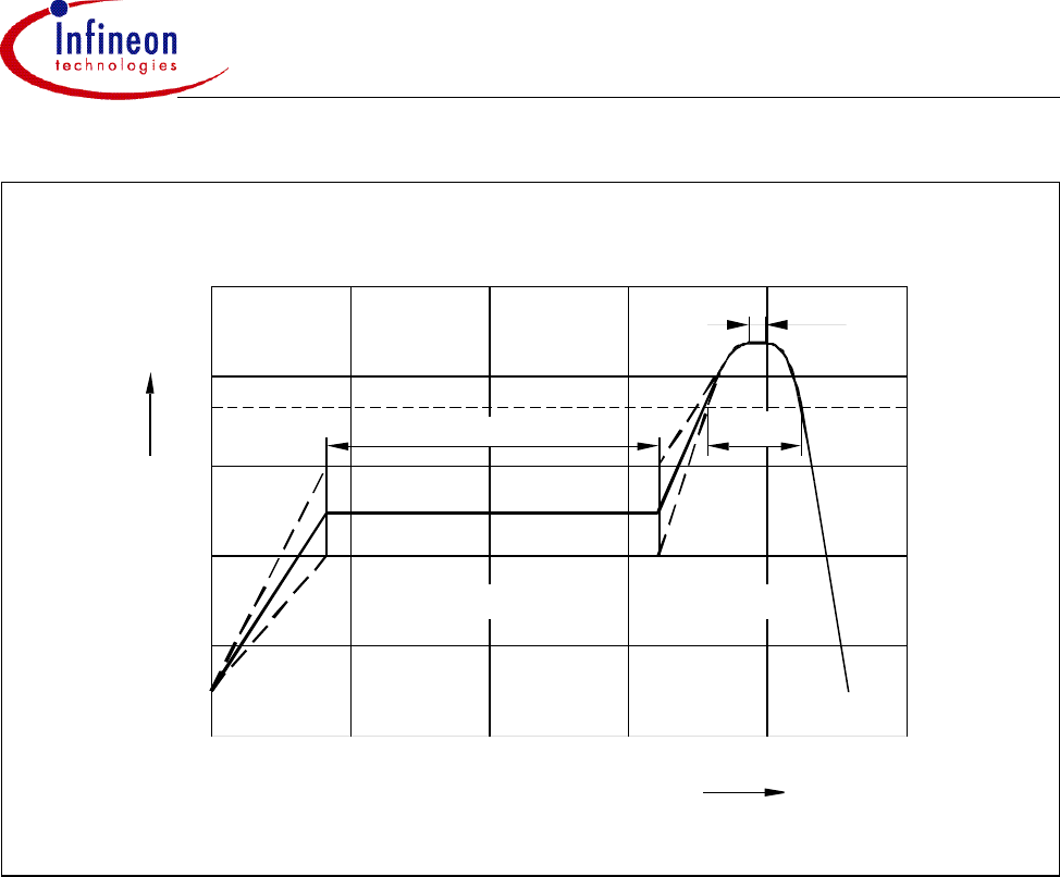
3.7.2 Soldering Profile
It must be noted that the module should not be allowed to be hanging upside down in the
reflow operation. This means that the module has to be assembled on the side of the
PCB that is soldered last. The reflow process should be a regular surface mount
soldering profile (full convection strongly preferred), the ramp-up should not be higher
than 3°C/s and with a peak temperature of 210 - 225°C during 10 - 20 seconds. Max
sloping rate should not be higher than 4°C/s (see example of reflow profile in Figure11).
ROK104001
Functional Description
Data Sheet 25 DS2, 2003-05-16
Figure11 Eutectic SnPb-Solder Profile
3.7.3 Placement
The recommended pickup coordinates for the ROK104001 shield is based on a nozzle
with inner diameter 2 mm and outer diameter 3.17 mm. The center of the shield is the
origin of coordinates, (0,0) for (x,y), giving the pickup coordinates (-1 mm,0) for (x,y).
3.7.4 Storage
Keep the component in its dry pack when not yet using the reel. After removal from the
dry pack ensure that the modules are soldered onto the PCB within 48 hours.
3.8 FCC Modular Approval
This device complies with part 15 of the FCC Rules. Operation is subject to the following
two conditions: (1) This device may not cause harmful interference, and (2) this device
must accept any interference received, including interference that may cause undesired
operation.
Changes or modifications not expressly approved by the party responsible for
compliance could void the user’s authority to operate the equipment.
ERA00106
120 s max.
0
050 100 150 200 250
50
100
150
200
250
s
t
T
°C
183°C
60-125 s
10-20 s
Max. rising 3°C/s Max. sloping 4°C/s
Temperature Profile

ROK104001
Functional Description
Data Sheet 26 DS2, 2003-05-16
The modular transmitter is labeled with its own FCC ID number, but, if the FCC ID is not
visible when the module is installed inside another device, then the outside of the device
into which the module is installed must also display a label referring to the enclosed
module. The exterior label can use wording such as the following: “Contains Transmitter
Module FCC ID: Q23104001” or “Contains FCC ID: Q23104001”. Any similar wording
that expresses the same meaning may be used.
When reusing the Modular Approval, antenna related measurements might need to be
redone.The antenna used for modular approval was a max 1.6dBi half-wave antenna
from gigAnt (PCB Swivel 6076019). When using an other antenna a class II permissive
change will be needed.
3.9 R&TTE Approval
This device complies with the requirements in the European Union and EFTA according
to the following test specifications:
EN 300 328
EN 60950 and EU standard
EN 301 489 -1/17
The R&TTE Approval for the ROK 104001-device is valid in the 19 member states of EU
and EFTA. The R&TTE-organizations of respective member state must be given 4
weeks of notice before a product based on this approval is allowed to be released to
market. Each state has its specific form to be filled in and submitted, for the respective
R&TTE organization to respond to. In the absence of any response within four weeks,
the product is allowed to be released to the market.
ROK104001
Electrical Characteristics
Data Sheet 27 DS2, 2003-05-16
4Electrical Characteristics
4.1 Absolute Maximum Ratings
Table3 Absolute Maximum Ratings
Parameter Symbol Values Unit
min. max.
Temperature
Storage temperature TStg -40 +125 °C
Maximum temperature -40 +85 °C
Operating temperature -20 +75 °C
Power Supply1)
1) VDDIO supply voltage must be powered on prior to or simultaneously as the VDD supply voltage. Deviations
from this power up sequence might damage the device.
Supply voltage VDD -0.3 5.25 V
Supply voltage (921k baud rate with turbo ON and
ECP firmware)
VDD -0.3 4.75 V
I/O Supply voltage VDD_IO -0.8 3.6 V
Baseband Digital I/Os
IO voltage range VIOP1 -0.3 +2.8 V
IO voltage range VIOP2 -0.3 VDD_IO
+ 0.3
V
Input clamp current VI < VSSIO or VI > VDDIO IIC -20 +20 mA
Output clamp current VO < VSSIO or VO > VDDIO IOC -20 +20 mA
Antenna Port
Matching on ANT pad (VSWR) 10 NA
Input RF power - In-band
- Out of band
15
15
dBm
dBm
ROK104001
Electrical Characteristics
Data Sheet 28 DS2, 2003-05-16
4.2 DC Specifications
Table4 DC Specifications
Unless otherwise noted, the specification applies for HCI firmware
TAmb = -20 to +75°C, 3.10 < VDD < 4.75 V, ON = 3.3V, VSWR ≤ 21)
Parameter Note/ Test
Condition Symbol Values Unit
min. typ. max.
Digital Inputs
Low level input
voltage, digital
input
Guaranteed
input low except
ON signal
VIL_IOP1 VSSIO - 0.3 0.85 V
VIL_IOP2 VSSIO - 0.3 0.3 x
V
DD_IO
V
ON signal only VIL 00.4 V
High level input
voltage, digital
input
RESET#2)
Guaranteed
input high
except ON
signal
VIH_IOP1 1.96 2.8 V
VIH_IOP 0.7 x
V
DD_IO
V
DD_IO
+ 0.3 V
ON signal only VIH 1.4 VDD V
Input pin internal
pull-up resistor
Input pin internal
pull-down resistor
(internal resistor
on baseband
chip)
(internal resistor
on baseband
chip)
RPU
RPD
30
10
50
20
80
40
kΩ
Ω
Digital Outputs
Low level output
voltage
IOL = 800 µA VOL 0VSSIO + 0.1 V
High level output
voltage
IOH = -800 µA VOH_IOP1 2.4 2.8 V
VOH_IOP2
V
DD_IO
- 0.1
V
DD_IO
V
Current Consumption
Input leakage cur-
rent, any digital in-
put or bidirectional
pin in input mode
VI = VSSIO -1 +1 µA
VI = VDDIO
Output leakage
current, tri-state
VO = VSSIO -1 +1 µA
VO = VDDIO
HW Shutdown3) 65 µA
ROK104001
Electrical Characteristics
Data Sheet 29 DS2, 2003-05-16
Idle state with stop
mode4)
during first 4 s. 1100 µA
after 4 s. 270 µA
Page Scan with
stop mode5) 3mA
Inquiry and Page
Scan with stop
mode5)
3mA
Hold mode5) during first 4 s. 1100 µA
after 4 s. 270 µA
Park mode5) 4.2 mA
Sniff mode6) 4.2 mA
Connection Mode7) 57600bps
460800bps
or 921600bps
with TURBO
off8)
921600bps
with TURBO
on8)
93
100
125
mA
mA
mA
VDDIO supply ICC_IO 2mA
1) Parameter errors may occur if VSWR > 2.
2) RESET# signal must be fed from an open drain output.
3) Current consumption is based upon where the ‘ON’ signal is low and ‘VDDIO’ is grounded.
4) After HCI command.
5) Inquiry and page mode current is measured during 1.28 s.
6) Sniff max & min interval: 1.28 s; Sniff attempt & Timeout: 19.375 ms.
7) Average current consumption measured during DH5 packet whilst in remote loop back configuration.
8) The HCI command turbo on has a typical throughput of 610 kbit/s but when the turbo command is off the baud
rate is reduced to 510 kbit/s.
Table4 DC Specifications (cont’d)
Unless otherwise noted, the specification applies for HCI firmware
TAmb = -20 to +75°C, 3.10 < VDD < 4.75 V, ON = 3.3V, VSWR ≤ 21)
Parameter Note/ Test
Condition Symbol Values Unit
min. typ. max.
ROK104001
Electrical Characteristics
Data Sheet 30 DS2, 2003-05-16
Table5 Timing Performance
Type Parameter/
Condition
Symbol Values Unit
min. typ. max.
Digital input pins
requirements1)
1) Static data - All baseband input and bi-directional pins can be connected to any external driving circuit before
turning on the supply, without damaging the device. However, it cannot be guaranteed that ROK104001 does
not load the external driver in this case, unless the baseband core supply voltage is completely discharged
prior to this event.
All digital input and bi-
directional input pins2)
2) Rise and fall times are measured between 10 % to 90 % of the VDDIO level.
Rise time tr 10 ns
Fall time tr 10 ns
Digital output pins
characteristics1)
All digital output and bi-
directional output pins2)
Rise time
CLOAD = 25 pF
tR3.5 20 ns
Fall time
CLOAD = 25 pF
tF3.5 15 ns
System
Clock frequency fSYS_CLK 13.0000 MHz
Clock frequency tolerance3)
3) Tolerance for the system clock takes into account aging effects of the crystal.
-20 +20 ppm
Start-up time from power on 250 ms
RESET# signal duration4)
4) RESET# signal must be fed from an open drain output.
Sink current >
1 mA
1ms
ROK104001
Electrical Characteristics
Data Sheet 31 DS2, 2003-05-16
Table6 ACL Packets
Parameter Condition Values Unit
min. typ. max.
Symmetric transfer rate DM1 packet 108 108 kb/s
DH1 packet 172 172 kb/s
DM3 packet 258 258 kb/s
DH3 packet 390 390 kb/s
DM5 packet 286 286 kb/s
DH5 packet 433 433 kb/s
Asymmetric transfer rate
Forward mode
DM1 packet 108 108 kb/s
DH1 packet 172 172 kb/s
DM3 packet 387 387 kb/s
DH3 packet 585 585 kb/s
DM5 packet 477 477 kb/s
DH5 packet1) 610 723 kb/s
Asymmetric transfer rate
Reverse mode
DM1 packet 108 108 kb/s
DH1 packet 172 172 kb/s
DM3 packet 54 54 kb/s
DH3 packet 86 86 kb/s
DM5 packet 36 36 kb/s
DH5 packet 57 57 kb/s
1) The HCI command turbo on has a typical throughput of 610 kbit/s but when the turbo command is off the baud
rate is reduced to 510 kbit/s. HCI turbo on command is only valid during 921k UART baud rate.
Table7 SCO Packets
Parameter Condition Values Unit
min. typ. max.
Maximum transfer rate HV1 packet 64.0 kb/s
HV2 packet 64.0 kb/s
HV3 packet 64.0 kb/s
DV packet 57.6 kb/s
ROK104001
Electrical Characteristics
Data Sheet 32 DS2, 2003-05-16
Table8 PCM interface Requirements and Characteristics
Parameter Symbol Values Unit
min. typ. max.
PCM Master mode (PCMCLK and PCMSYNC are outputs)
PCM clock frequency fPC 2000 kHz
PCM clock high period tPCH 200 ns
PCM clock low period tPCL 200 ns
PCMSYNC pulse valid from PCMCLK rising edge tPSV 100 ns
PCMSYNC pulse hold time from PCMCLK falling
edge
tPSH 200 ns
PCMX data out valid from PCMCLK rising edge tPDOV 100 ns
PCMX data in setup time to PCMCLK falling edge tPDIS 100 ns
PCMX data in hold time from PCMCLK falling
edge
tPIDH 100 ns
PCM Slave mode (PCMCLK and PCMSYNC are inputs)
PCM clock frequency fPC 200 2048 kHz
PCM clock high period tPCH 200 ns
PCM clock low period tPCL 200 ns
PCMSYNC setup time to PCMCLK falling edge tPSS 100 ns
PCMSYNC hold time from PCMCLK falling edge tPSH 100 ns
PCMSYNC pulse width tPSW 1/fPC ns
PCMX data out valid from PCMCLK rising edge tPDOV 100 ns
PCMX data in setup time to PCMCLK falling edge tPDIS 100 ns
PCMX data in hold time from PCMCLK falling
edge
tPIDH 100 ns
Table9 RF Specifications
Parameter Condition Values Unit
min. typ. max.
General
Frequency range
2.402 2.480
GHz
Double sided IF bandwidth 1MHz
ROK104001
Electrical Characteristics
Data Sheet 33 DS2, 2003-05-16
Antenna load 50 Ω
VSWR Rx mode 2:1
VSWR1) Tx mode 2:1
Receiver Performance
Sensitivity level DH1 Connection
160 kHz deviation
w.r.t. BER < 0.1 %
-75 -71 dBm
Max input level -20 +13 dBm
RSSi accuracy Pin = -40 dBm -6 0+6 dB
Pin = -60 dBm -6 0+6 dB
C/Ico-channel2) 3) 12 14 dB
C/I1MHz
2) 3) -3 0dB
C/I2MHz
2) 4) -35 -30 dB
C/I>3MHz2) 4) -50 -30 dB
C/Iimage2) 4) -20 -9 dB
Adjacent (1 MHz) interference to
inband image frequency
C/Iimage+/-1MHz
2) 4)
-30 -20 dB
Out-of-band blocking 30-1850 MHz +5 +15 dBm
1850-1910 MHz +4 +15 dBm
1911-2000 MHz 0+9 dBm
2001-2399 MHz -27 -8 dBm
2484-2999 MHz -27 -9 dBm
3.0-12.75 GHz -10 +3 dBm
Intermodulation rejection2) 5) -39 -30 dBm
Spurious emissions 30 MHz to 1 GHz -57 dBm
1 GHz to 12.75 GHz -47 dBm
Transmitter Performance
Frequency deviation 140 160 175 kHz
Tx power -4 +1 +4 dBm
Initial frequency error -75 0 75 kHz
20 dB bandwidth with peak detector 1000 kHz
Table9 RF Specifications (cont’d)
Parameter Condition Values Unit
min. typ. max.
ROK104001
Electrical Characteristics
Data Sheet 34 DS2, 2003-05-16
Tx carrier drift 2402 to 2482 MHz 1 slot (366 µs) -25 25 kHz
3 slots (1598 µs) -40 40 kHz
5 slots (2862 µs) -40 40 kHz
Tx carrier drift 2480 to 2402 MHz 1 slot (366 µs) -25 25 kHz
3 slots (1598 µs) -40 40 kHz
5 slots (2862 µs) -40 40 kHz
Drift rate -20 20 kHz
Adjacent channel power +2 MHz -20 dBm
-2 MHz -20 dBm
+3 MHz -40 dBm
-3 MHz -40 dBm
+4 MHz -40 dBm
-4 MHz -40 dBm
+13 MHz -40 dBm
-13 MHz -40 dBm
Spurious emissions 30 MHz - 1 GHz -36 dBm
1 GHz - 12.75 GHz -30 dBm
1.8 GHz - 1.9 GHz -47 dBm
5.15 GHz - 5.3 GHz -47 dBm
1) During the Tx mode, the VSWR specification states the limits that are acceptable before any other RF
parameters are strongly affected, i.e. frequency deviation and drift.
2) Specification only valid for normal test conditions TAMB = 15 - 35 C.
3) Carrier signal level of -60 dBm, interferer Bluetooth modulated.
4) Carrier signal level of -67 dBm, interferer Bluetooth modulated.
5) Carrier: -64 dBm @ 2441 MHz, 1st
interferer: CW @ 2446 MHz, 2nd interferer: BT mod. @ 2451 MHz.
Table9 RF Specifications (cont’d)
Parameter Condition Values Unit
min. typ. max.

ROK104001
Marking
Data Sheet 35 DS2, 2003-05-16
5Marking
5.1 Module Marking
Each module shall be marked with the following information printed on the shield.
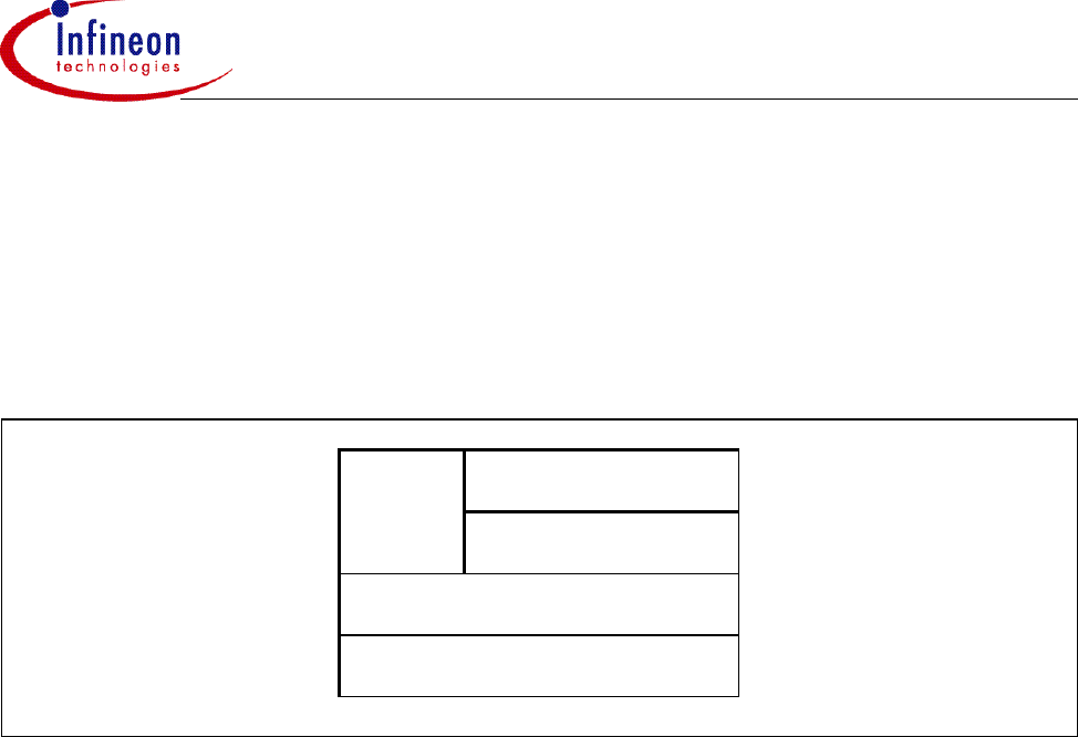
Table10
Marking Description
1: Infineon logotype
2:
<ROK104001/21 R1A
>Product number with suffix and revision state acc to
purchase order
3: <bbbbbb> Batch number
4: <yyww2> Manufacturing year (yy), week (ww) and factory code (2)
5:
Bluetooth logotype.
6: CE-logo.
7:FCC ID: Q23104001 FCC No.
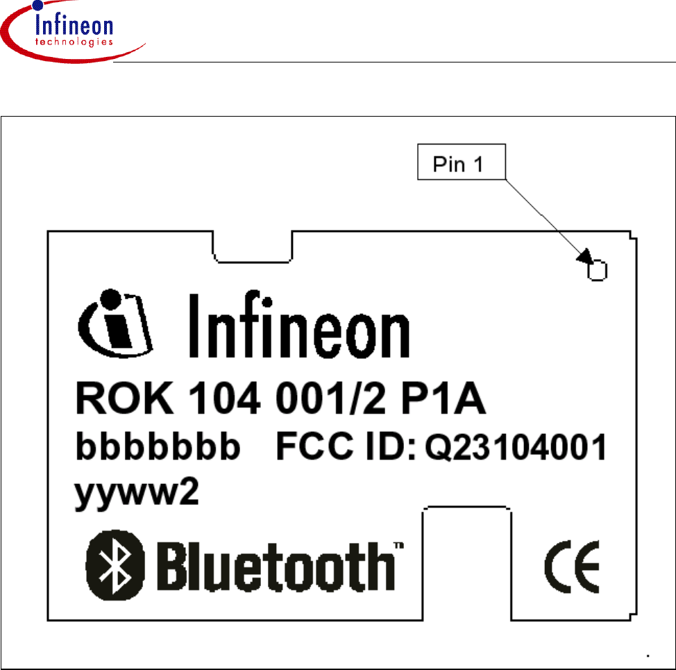
ROK104001
Marking
Data Sheet 36 DS2, 2003-05-16
Figure12 Module Marking
5.2 Reel Marking
The reel, reel box and dry pack has a label with the following information:
•Infineon product number with revision
•Customer product number with revision
•Quantity
•Reel-ID. (Batch No)
•Factory code
•Manufacturing date
•Country of origin
•Infineon logotype
1-6 above is also printed in BAR-code format
ROK104001
Package Outlines
Data Sheet 37 DS2, 2003-05-16
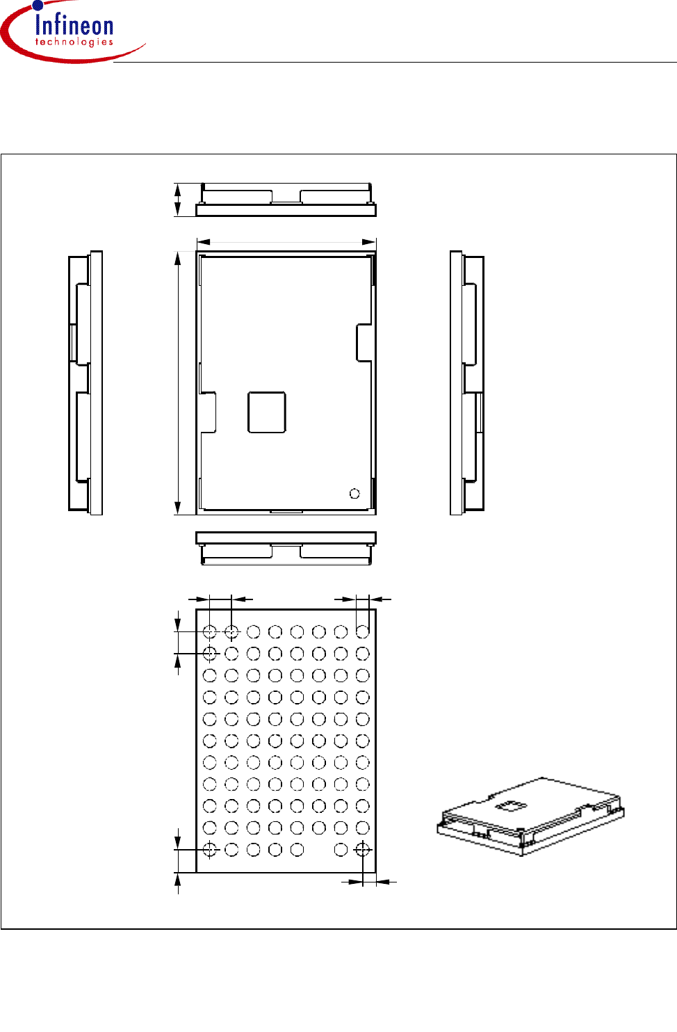
6Package Outlines
Figure13 ROK104001 Mechanical Dimensions (maximum values) and
Footprint, Bottom View
ERA00108
15.5 ±0.2 2 max.
1.27
1.27
0.8 typ.
0.805
1.4
10.5
±0.2
You can find all of our packages, sorts of packing and others in our
Infineon Internet Page “Products”: http://www.infineon.com/products.Dimensions in mm
ROK104001
Package Outlines
Data Sheet 38 DS2, 2003-05-16
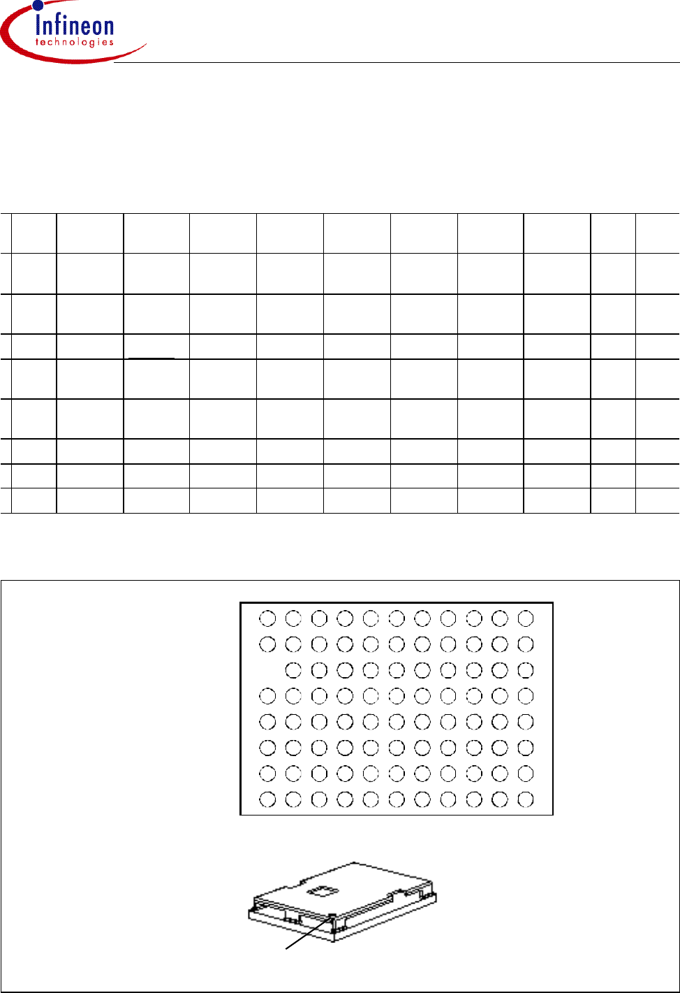
6.1 Pinout (bottom view)
Please refer to Figure4 for the positioning of each pad.
6.2 Footprint, Land View
Figure14 ROK104001 Mechanical Dimensions of Footprint,
Land Pattern View (seen from above the component)
Table11
7GND N.C. N.C. N.C. VDD_RF
DIG GND N.C. N.C. N.C. N.C. GND
6GND SERIAL
DATA GPIOB7 GPIOB6 N.C. -
VTP3 N.C. -
VTP4 GND GND GND GND GND
5GND N.C. -
VTP1
PWRFAIL
N.C. -
VTP2
UART2RTS
PWRAV
AIL N.C. N.C. VDD GND GND
4GND N.C. GPIOB2
DETACH
GPIOB4 N.C. GND
UART1Tx
VDDIO ON N.C.
3GND GND RESET SERIAL
CLK GPIOB5
UART1Rx WAKEUP
UART1RTS UART1CTS
D+ N.C.
2ANT GND EXTSYS
WAKEUP UART2Rx
EXTINT
PCMSYNC
N.C.
UART2CTS
D- GND
1GND GND GND GPIOB3 PCMTX
PCMCLK
PCMRx N.C.
UART2Tx
GND GND
0GND N.C.
N.C. - VTP5
N.C. N.C. GND N.C. N.C. N.C. N.C. GND
VTRPNMLKJHG
ERA00109
VTRPNMLKJHG
7
6
5
4
3
2
1
0Pad Size: ø0.8 mm
Pitch: 1.27 mm
G0

ROK104001
Ordering Information
Data Sheet 39 DS2, 2003-05-16
7Ordering Information
Please contact Infineon Technologies for further information.
8Packaging
The modules will be delivered in a tape & reel and dry pack, protecting them from ESD
and mechanical shock.
The tape width is 24 mm and the pitch is 12 mm. The diameter of the reel is 13 inches
and it contains 1500 modules.
9Abbreviations
ASIC - Application Specific Integrated Circuit
BER - Bit Error Rate
CMOS - Complementary Metal Oxide Semiconductor
DCE - Data Circuit terminating Equipment
HCI - Host Controller Interface
IC - Integrated Circuit
ISM - Industrial Scientific and Medical
LGA - Land Grid Array
PCB - Printed Circuit Board
PCM - Pulse Code Modulation
Rx - Receive
SIG - Special Interest Group
Tx - Transmit
UART - Universal Asynchronous Receiver Transmitter
USB - Universal Serial Bus