Intel Mobile Communications 31307 Wireless Bluetooth module User Manual Product Overview Singlestone PA33
Intel Mobile Communications GmbH Wireless Bluetooth module Product Overview Singlestone PA33
Users Manual

Preliminary Data Sheet, 11/2001 CONFIDENTIAL
Never stop thinking.
Secure Mobile Solutions
Preliminary Product Overview
T3130-7V10PO1-7600
Apr-2004
PBA 313 07
Singlestone

Singlestone
PBA 313 07
Preliminary Product Overview 4/2004
2
For questions on technology, delivery and prices please contact the Infineon Technologies Offices in Germany or the Infineon
Technologies Companies and Representatives worldwide: see our webpage at http://www.infineon.com
ABM®, AOP®, ARCOFI®, ARCOFI®-BA, ARCOFI®-SP, DigiTape®, EPIC®-1, EPIC®-S, ELIC®, FALC®54, FALC®56, FALC®-E1,
FALC®-LH, IDEC®, IOM®, IOM®-1, IOM®-2,IPAT®-2, ISAC
®-P, ISAC
®-S, ISAC
®-S TE, ISAC
®-P TE, ITAC
®, IWE
®, MUSAC
®-A,
OCTAT®-P, QUAT®-S, SICAT®, SICOFI®, SICOFI®-2, SICOFI®-4, SICOFI®-4µC, SLICOFI®, are registered trademarks of
Infineon Technologies AG.
ACE™, ASM™, ASP™, POTSWIRE™, QuadFALC™, SCOUT™ are trademarks of Infineon Technologies AG.
BLUETOOTHTM
is a trademark owned by its proprietor and used by Infineon Technologies AG under license.
Edition 4/2004
Published by Infineon Technologies WS Sweden AB,
Isafjordsgatan 16
SE-164 81 Kista
© Infineon Technologies AG
All Rights Reserved.
Attention please!
The information presented in this document does not constitute a part of any quotation or contract. Infineon Technologies
especially emphazises the following:
As far as patents or other rights of third parties are concerned, liability is expressly excluded for applications, processes and
circuits implemented within components or assemblies.
The information describes the type of component and shall not be considered as assured characteristics or representation.
Terms of delivery and rights to change design reserved.
Due to technical requirements components may contain dangerous substances. For information on the types in question please
contact your nearest Infineon Technologies Office.
Infineon Technologies AG is an approved CECC manufacturer.
Packing
Please use the recycling operators known to you. We can also help you - get in touch with your nearest sales office. By
agreement we will take packing material back, if it is sorted. You must bear the costs of transport.
For packing material that is returned to us unsorted or which we are not obliged to accept, we shall have to invoice you for any
costs incurred.
Components used in life-support devices or systems must be expressly authorized for such purpose!
Critical components1 of the Infineon Technologies AG, may only be used in life-support devices or systems 2 with the express
written approval of Infineon Technologies AG.
1 A critical component is a component used in a life-support device or system whose failure can reasonably be expected to
cause the failure of that life-support device or system, or to affect its safety or effectiveness of that device or system.
2 Life support devices or systems are intended (a) to be implanted in the human body, or (b) to support and/or maintain and
sustain human life, such as, for example, in medical, air traffic, defense, or life-sustaining automotive applications. If they fail, it
is reasonable to assume that the health of the user or another person may be endangered.
Exclusion of Warranty and Liability
The Software is provided "as is" and Infineon gives no warranty - expressly or implied - of any kind, including, but not limited to,
warranties of merchantability or fitness for a particular purpose, nor does Infineon assume any liability whatsoever as to the
performance of the Software.
In addition, Infineon assumes no responsibility for the ability of the customer to use this Software for the purpose it was provided
for, nor does Infineon assume responsibility for any claims, including, but not limited to, claims of infringement of intellectual
property rights of third parties, arising from the customer's use of the Software.

Singlestone
PBA 313 07
Preliminary Product Overview 4/2004
3
Table of Contents
1Introduction...................................................................................................................... 5
2General Device Overview.............................................................................................. 6
2.1 General Features.............................................................................................................7
2.2 Block diagram.................................................................................................................8
2.3 Typical application .........................................................................................................8
2.4 Mechanical dimension and pad arrangement.................................................................9
2.5 Module pin-out..............................................................................................................10
2.6 Functional Block Diagram ............................................................................................11
2.7 System Integration and Applications............................................................................12
2.7.1 General description..................................................................................................12
3Electrical Specifications .............................................................................................13
3.1 Absolute Maximum Ratings..........................................................................................13
3.2 Operating conditions....................................................................................................13
3.3 Latch-up immunity........................................................................................................13
3.4 Quality ..........................................................................................................................13
3.5 Capacitance..................................................................................................................14
3.6 Current consumption....................................................................................................14
3.7 DC Characteristics of Digital Part.................................................................................15
3.7.1 Pull Up characteristics on ResetQ.............................................................................16
3.8 Operational Range for RF part......................................................................................16
3.9 AC/DC Characteristics of RF part..................................................................................16
3.9.1 Transmitter Characteristics.......................................................................................17
3.9.2 RSSI.......................................................................................................................17
3.9.3 Receiver Characteristics...........................................................................................18
3.10 Characteristics of externally supplied 32.768kHz clock signal...............................18
4Assembly and design guidelines .............................................................................19
4.1 General description of the module ...............................................................................19
4.2 Printed Circuit Board design.........................................................................................19
4.3 Solder paste printing ....................................................................................................19
4.4 Assembly......................................................................................................................20
4.4.1 Component placement .............................................................................................20
4.4.2 Pin mark..................................................................................................................20
4.5 Soldering profile...........................................................................................................21
4.6 Antenna ........................................................................................................................21
4.7 Shielding / EMC requirements.......................................................................................21
4.8 Safety............................................................................................................................21
5Type approvals and Qualification.............................................................................22
5.1 Bluetooth Qualification.................................................................................................22

Singlestone
PBA 313 07
Preliminary Product Overview 4/2004
4
5.2 FCC Modular Approval..................................................................................................22
5.3 R&TTE Approval...........................................................................................................22
6Module marking.............................................................................................................23
7Package...........................................................................................................................24
8References......................................................................................................................25

Singlestone
PBA 313 07
Preliminary Product Overview 4/2004
5
1 Introduction
The module is built around the BlueMoon Single Cellular chip (PMB 8761) which contains the radio,
baseband, link manager and HCI functionality. For additional information regarding the PMB8761 such
as firmware features, complete description of Infineon specific HCI commands and events, please
refer to the latest version of the Data sheet for PMB8761, T8761-XV01Dx-7600.

Singlestone
PBA 313 07
Preliminary Product Overview 4/2004
6
2 General Device Overview
Infineon’s Singlestone - PBA 313 07 is a ready-to-use Class2 Bluetooth module solution targeted for
data and audio applications in the 10 meters personal area range.
BLUETOOTH wireless technology is an open industry standard for short range wireless
communication with both data and voice transmission capability (up to 723 kbit/s data asymmetrically
or up to 3 voice channels simultaneously). Singlestone is a Bluetooth 1.1 pre-qualified component, so
any further development and qualification efforts for the user are minimized. It is already hardware
prepared for the upcoming Bluetooth 1.2 Standard, which will improve the quality of voice connections,
support the co-existence with WLAN solutions using the same frequency band and accelerate the
connection setup.
Integrating the baseband, link manager and RF-transceiver, Singlestone closes the gap between the
Bluetooth air interface (external antenna, 2.4 GHz ISM band) and the standardized host-controller-
interface (HCI), which is physically realized as a full-duplex UART port (HW-handshake optional). In
parallel, the PCM interface is suitable for audio connections.
Around Infineon’s BlueMoon Single Cellular – PMB 8761 Bluetooth chip, all essential components for
a complete Bluetooth solution are integrated in the Singlestone module. A 26 MHz temperature
compensated crystal oscillator (TCXO) provides the highly accurate Bluetooth clock, an E²PROM
holds the application specific configuration data which is loaded after power-up reset, and an
integrated balun-filter component ensures optimized RF matching between the chip and the external
antenna. Only a 32.768 kHz real-time clock, which is available in most target applications, must be
provided to the Singlestone module.
Bluetooth stack software supporting the extended feature set of Infineon’s BlueMoon family and a
comprehensive portfolio of Bluetooth profiles are available from our SW partners ported to a variety of
host architectures.
The device is designed for a broad range of wireless applications in the consumer, automotive and
industrial segments, as well as for interconnection of cellular phones, desktop PCs, laptops, and
PDAs.
The device is available in a shielded LGA package (11.85 x 10.6 mm²) with 8x9 pads.

Singlestone
PBA 313 07
Preliminary Product Overview 4/2004
7
2.1 General Features
General
• Low power consumption, programmable Power down mode
• Chip in advanced low power CMOS technology
• External supply-voltage 3.0V..4.75 V, recommended 3.3 V +/- 5 %
• Extended temperature range – 40°C .. +85°C
Interfaces
• UART for UART-HCI with HW-handshake (Baudrate up to 3 Mbaud)
• PCM interface (slave- and master-mode; programmable PCM slot allocation)
• JTAG
• GPIO for control of external devices
Digital-Section
• Digital demodulation gives best performance in sensitivity, co- and adjacent channel performance
• Digital offset compensation and symbol synchronization / frame synchronization
• GFSK-modulator (over-sampling at typ. 9-bit-resolution) with amplitude adjustment and high-
performance A/D-converter for RX-data
• Digital part (Noise-shaper, Gaussian impulse filter) of Σ∆-Fractional-N-PLL
• CVSD transcoder for voice conformant to BLUETOOTH wireless technology
• A-law, u-Law and linear PCM also possible
• Baseband and Linkmanager Firmware up to HCI in internal ROM
• 4 kbit E2PROM for storing Bluetooth device data
RF and Analog Section
• Analog part of Σ∆-Fractional-N-PLL for receive and transmit path (multi-modulus-divider, phase
detector and charge pump) on chip
• Fully integrated and balanced VCO with integrated varactors and inductors.
• On chip 2.5 GHz RF driver amplifier up to + 5 dBm output power (Fine tuning in the range of -16 - +
5 dBm in 1.5 dB steps)
• Integrated LNA
• Fully integrated Balun, switch and antenna filter giving one single-ended RF interface, no additional
external RF components
• Chip-integrated supply voltage regulator for VCO
• On module 26 MHz reference clock
• On module voltage regulator for single supply voltage.
• Typical sensitivity -83 dBm
• Typical output power +2.5 dBm
Software
• Baseband, Link Manager and HCI functionality is incorporated by ProBlue Firmware in chip-
integrated ROM.
• Infineon specific HCI+ commands to support enhanced features
• Configuration data (e.g. Bluetooth device address) are loaded from internal E2PROM after reset.
Optionally, configuration data may be provided by the host via HCI+ command.
Package
• LGA 9 x 8 pads
Singlestone
PBA 313 07
Preliminary Product Overview 4/2004
8
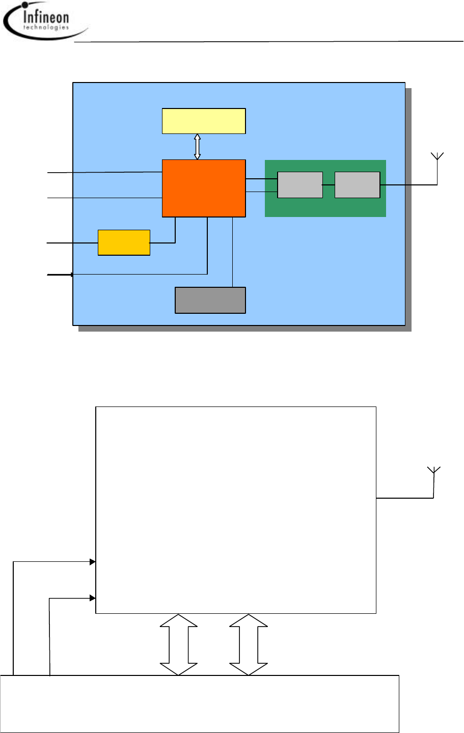
2.2 Block diagram
V
supply
Singlestone
– PBA 313 07
EEPROM
I
2
C
PMB8761
Bluemoon
Single
Cellular
Voltage
Regulator
PCM
UART HCI
Clock
26 MHz
Low Power
Clock
32.768
kHz
Balun
Antenna
Filter
Antenna
Figure 2-1: Block diagram of the PBA 313 07 Singlestone module
2.3 Typical application
UART
PCM
V
Supply
Host application
CLK32
PBA 313 07
Bluetooth
Module
Singlestone
Figure 2-2: Typical application diagram
Singlestone
PBA 313 07
Preliminary Product Overview 4/2004
9
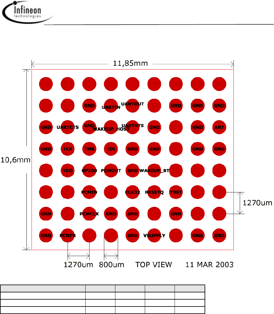
2.4 Mechanical dimension and pad arrangement
Below shows the module’s pad layout. All dimensions are in mm.
A B C D E F G H J
7
6
5
4
3
2
1
0
Figure 2-3 Mechanical dimensions, pad arrangement.
Dimension min. typ. max. Unit
Length 11.65 11.85 12.05 mm
Width 10.40 10.6 10.80 mm
Height 1.6 1.8 2.0 mm
Table 2-1 Mechanical dimensions with tolerances
Singlestone
PBA 313 07
Preliminary Product Overview 4/2004
10
2.5 Module pin-out
Table 2-2 represents the functional description of Singlestone’s connecting pads. Functionally non-
used pads (NC) are used as sacrifice pads or test pads, and must not be connected in an application.
Pin Location Symbol Input/
Output
During
Reset After
Reset Function
Comments
D6 UARTIN I Tristate Tristate UART-Input
E6 UARTOUT O Pull-Up Pull-Up UART-Output (Pull-Up controlled by
FW)
E5 UARTRTS O Pull-Down Pull-Down UART-Request to Send (Pull-
Down/-Up controlled by FW)
B5 UARTCTS I Tristate Tristate UART-Clear to Send
D5 WAKEUP_HOST O Pull-Down Pull-Down Wake-up signal for host ) (Pull-
Down controlled by FW)
C2 PCMIN I Tristate Tristate PCM input
D3 PCMOUT O Pull-Down Pull-Down PCM output (Pull-Down/-Up
controlled by FW)
B0 PCMFR I/O Pull-Down Pull-Down PCM frame (8kHz)(Pull-Down/-Up
controlled by FW)
C1 PCMCLK I/O Pull-Down Pull-Down PCM clock (>64kHz) (Pull-Down/-
Up controlled by FW)
C3 GPIO
(=GPIO0)
I/O Pull-Down Pull-Down General purpose Input/Output (Pull-
Down/Up controlled by FW)
G2 TRST I Pull-Down Pull-Down Test Reset (JTAG)
B4 TCK I Input Input Test Clock (JTAG)
C4 TMS I Pull-Up Pull-Up Test Mode Set (JTAG)
D4 TDI I Pull-Up Pull-Up Test Data Input (JTAG)
B3 TDO O Tristate Tristate Test Data Output (JTAG)
F2 RESETQ I Pull-Up Pull-Up Reset line (0:reset, 1:active)
F3 WAKEUP_BT I Input Input Wake-up signal from low power
mode
E2 CLK32 I Input Input 32.768 kHz clock input
J5 ANT A RF input /output 50 ohms.
F0 VSUPPLY S Power Supply
G7 NC (VDD) Regulated supply voltage for test
purposes. Important that is leaved
NC.
A0, A1, A4, A5 GND
C5, C6 GND
D1 GND
E0, E1 GND
E3, E4 GND
F4, F5 GND
G1, G6 GND
H0, H4, H5, H6 GND
J0, J4, J6 GND
A2, A3 , A6, A7 NC
B1, B2, B6, B7 NC
C0, C7 NC
D0, D2, D7 NC
E7 NC
F1, F6, F7 NC
G0, G3, G4, G5,
G7 NC
H1, H2, H3, H7 NC
J1, J2, J3, J7 NC
Table 2-2 Module pin-out
Singlestone
PBA 313 07
Preliminary Product Overview 4/2004
11
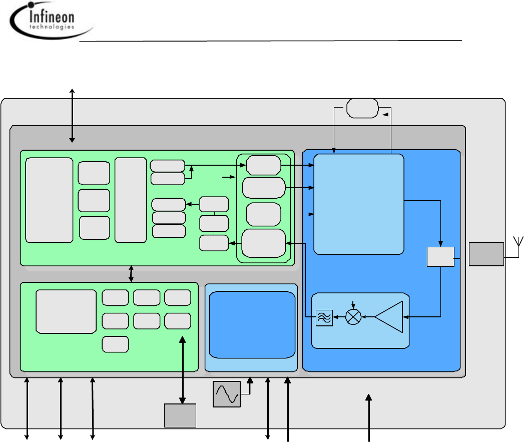
2.6 Functional Block Diagram
JTAG
GPIO
26 MHz XO
Digital Baseband
Section
Data
-
RAM/
Control
-
RAM
(Buffers)
Loop Filter
Demodulator
Antenna
Switch
Analog RF
-
Section
I
2
C
-
Interface
Analog Baseband Section
Σ∆-Clocks-PLL
Power management unit
Digital Link C
ontrol
Section
RF Frequency
Synthesizer
(Analog part of
Σ∆
-
Fractional
-
N
-
PLL)
&
Transmitter
UART
Σ∆
Fract.-N-
PLL
Control
Information
PCM-
Interface
A/
µ
-
Law
CVSD
Par a
Ser
Baseband
-
Control
CRC/FEC
CRC/FEC
Ser
a
Par
Frame-
Sync
Symbol-
Recov.
Offset-
Canc.
Timers/
RF
-
Interface
Impulse
Shaping
Bluetooth
Link
-
Control/
Link
-
Manager/
HCI
-
UART
Clocks
Timer
Watch
-
dog
Inter
-
rupts
Ports
I²C
UART
Receiver
LNA
PCM Interface
32.768 kHz
Encryption
Balun +
filter
E
2
PROM
VSUPPLY (3.0V
–
4.75
V)
WAKEUP
PMB8761 BlueMoon Single Cellular
Figure 2-4: Singlestone PBA 313 07 Block diagram

Singlestone
PBA 313 07
Preliminary Product Overview 4/2004
12
2.7 System Integration and Applications
2.7.1 General description
On the RF-side, Singlestone provides a 50 Ohm single-ended input/output to be directly connected to
an external antenna. The design of the antenna is open to a broad spectrum (e.g. PCB antenna,
ceramic antenna, external antenna) and can be optimized to the target application requirements.
The HCI-interface is implemented as a full-duplex UART port which can be configured to be used in 2-
line or 4-line mode (with or without hardware handshake). If hardware handshake is not used then the
UARTCTS pin must be grounded.
The PCM interface is able to serve one Bluetooth SCO channel for voice data. Optionally, SCO
channels may be linked to the host via the HCI-UART interface.
Both the UART- and PCM-interfaces are assigned to the regulated voltage (2.7V) powered by
VSUPPLY. VSUPPLY must be in the range of 3.0 to 4.75 V.
General purpose input/output lines (GPIOs) can be controlled via HCI+ commands.
Configuration data (e.g. Bluetooth device address) are loaded from internal E
2PROM after reset.
Optionally, configuration data may be provided by the host via HCI+ commands.
Singlestone
PBA 313 07
Preliminary Product Overview 4/2004
13
3 Electrical Specifications
3.1 Absolute Maximum Ratings
The maximum ratings may not be exceeded under any circumstances, not even momentarily and
individually, as permanent damage to the module will result.
Parameter Limit values Unit
min. max.
VSUPPLY Supply voltage range -0.3 6.0 V
VI Input Voltage Range -0.3 3.75 V
VO Output Voltage Range 0.3 3.0 V
IIN Input Current - 10 10 mA
ESD integrity according to MIL-STD883D
Method 3015.7 1 kV
TStorage Maximum storage temperature range -40 125 °C
Table 3-1: Absolute maximum ratings
Note: Stresses above those listed under "Absolute Maximum Ratings" may cause permanent damage
to the device. Exposure to conditions beyond those indicated in the recommended operational
conditions of this specification may affect device reliability. This is a stress rating only and
functional operation of the device under these conditions or at any other condition beyond those
indicated in the operational conditions of this specification is not implied.
3.2 Operating conditions
Unless otherwise stated, the following characteristics apply operating conditions.
Parameter min. typ. max. Remarks
Temperature -40°C +25°C +85°C
VSUPPLY 3.0V 3.3V 4.75V
Table 3-2 Operating Conditions
3.3 Latch-up immunity
Latch-up immunity is guaranteed in accordance with JEDEC-standard No. 17, EIA Jedec JC-40.2.
3.4 Quality
For quality and reliability conditions se 105 63-PBA31301+ Uen.
Singlestone
PBA 313 07
Preliminary Product Overview 4/2004
14
3.5 Capacitance
T = 25°C
Symbol Parameter Limit Values
min. max. Unit
CIN input capacitance -10 pF
COUT output capacitance -15 pF
CIO I/O -20 pF
Table 3-3: Capacitance
3.6 Current consumption
Regulator input voltage: VSUPPLY = 3.0..4.75V
Average Consumption #Bluetooth mode min. typ. max. Unit Test Conditions
1 HV3 32 40 mA ACL link in sniff mode with max.
interval
2WSE 0x02 2.2 3.5 mA 1.28 s scan interval, 11.25 ms
scan, no interlaced scan
3WSE 0x03 3.0 4 mA 1.28 s scan interval, 2*11.25 ms
scan, no interlaced scan
4Sniff mode 2 3 mA 2.00 s sniff interval, sniff attempt =
1, sniff timeout = 0
Table 3-4: Average current for some Bluetooth modes. WSE means after
HCI_Write_Scan_Enable.
Singlestone
PBA 313 07
Preliminary Product Overview 4/2004
15
3.7 DC Characteristics of Digital Part
VSUPPLY = 3.0V..4.75V.
Maximum allowed input levels are from -0.3V to 3.0V.
Higher voltages up to 3.6V can be applied at UARTIN, UARTCTS, PCMIN, PCMFR, PCMCLK, TRST,
TCK, TMS, TDI, RESETQ, CLK32, WAKEUP_BT.
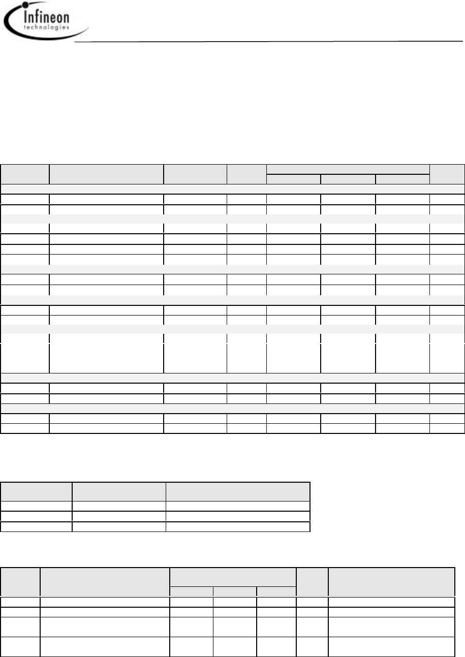
Symbol Parameter Test Condition Limit Values Unit
Min typ max
Pins: PCMCLK, PCMFR, PCMIN, UARTIN, UARTCTS, GPIO0
VIN LOW Input low voltage - - 0.81 V
VIN HIGH Input high voltage -1.89 -V
Pins: PCMCLK, PCMFR, PCMOUT, UARTOUT, UARTRTS, GPIO0
VOUT LOW Output low voltage IOL=2.4mA - - 0.68 V
VOUT LOW Output low voltage IOL=100µA- - 0.27 V
VOUT HIGH Output high voltage IOH=-2.4mA 2.02 - - V
VOUT HIGH Output high voltage IOH=-100µA2.43 - - V
Pins: WAKEUP_HOST
VOUT LOW Output low voltage IOL=100µA- - 0.27 V
VOUT HIGH Output high voltage IOH=-100µA2.43 - - V
Pins: TRST, TCK, TMS, TDI
VIN LOW Input low voltage - - 0.81 V
VIN HIGH Input high voltage -1.89 -V
Pin: TDO
VOUT LOW Output low voltage IOL=2.4mA -0.35 V
VOUT LOW Output low voltage IOL=100µA-0.15 V
VOUT HIGH Output high voltage IOH=-2.4mA 2.2 -V
VOUT HIGH Output high voltage IOH=-100µA2.6 -V
Pin: WAKEUP_BT, CLK32
VILOSC Input low voltage - - 0.4 V
VIHOSC Input high voltage -2.0 -V
Pin: RESETQ
VIN LOW Input low voltage - - 0.35 V
VIN HIGH Input high voltage -2.5 -V
Table 3-5: DC characteristics of digital part
max. Load Capacitance
(during test)
Rise/Fall Time (for measurement of
DC characteristics)
PCMOUT 30 pF 30 ns
PCMCLK 30 pF 30 ns
PCMFRM 30 pF 30 ns
Table 3-6: Pin characteristics
Symbol Parameter Limit
Values Unit Test Condition
min typ max
ILI Input leakage current - - 1µA 0V<V IN<2.7V
ILO Output leakage current - - 1µA 0V<V OUT <2.7V
ILI, H Input leakage current for 3.6V
tolerant pins* - - 1µA 0V<V IN<3.6V
ILO, H Output leakage current for UART
and PCM domain pins - - 1µA 0V<V OUT <2.7V
Table 3-7: Leakage currents
* The following pins are 3.6 V tolerant: UARTIN, UARTCTS, PCMIN, PCMFR, PCMCLK, TRST, TCK,
TMS, TDI, RESETQ, CLK32, WAKEUP_BT
Singlestone
PBA 313 07
Preliminary Product Overview 4/2004
16
Pull-Up and Pull-Down Values
Symbol Pull-Up Pull-Down Unit Test Condition
min typ max min typ max
UARTRTS 100 160 230 100 150 200 µA
UARTOUT 100 160 230 100 150 200 µA
WAKEUP_HOST 100 160 230 100 140 200 µA
PCMOUT 100 160 230 100 140 200 µA
PCMFR 100 160 230 100 140 200 µA
PCMCLK 100 160 230 100 140 200 µA
GPIO0 40 100 200 30 90 170 µA
Table 3-8: Pull-Up / Pull-Down characteristics
3.7.1 Pull Up characteristics on ResetQ
The ResetQ signal is pulled up to Vdd. In order for the chip to start up properly at power up the pull up
is delayed. Below is a table stating the delay from applying a stable Vsupply to the module until the
ResetQ goes high.
Parameter Limit
Values Unit Test Condition
min typ max
Delay pull up of ResetQ 26 50 µs
Pull-up current ResetQ 270 500 µA
3.8 Operational Range for RF part
Within the operational range the module operates as described in the circuit description. The AC/DC
characteristic limits are not guaranteed.
Note: Power levels refer to 50Ω impedance
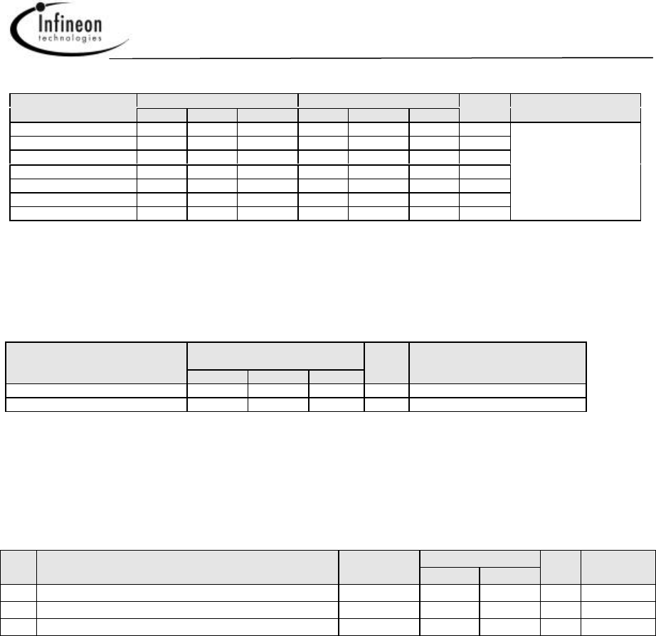
Limit values #Parameter Symbol min. max. Unit Remarks
1 RF input level PRFIN 10 dBm
2 RF input frequency fRFIN 2500 MHz
3 Ambient temperature TA -40 +85 °C
Table 3-9: Operational range for the RF part
3.9 AC/DC Characteristics of RF part
AC/DC characteristics involve the spread of values guaranteed within the specified supply voltage and
ambient temperature range. Typical values are the median of the production.
Singlestone
PBA 313 07
Preliminary Product Overview 4/2004
17
3.9.1 Transmitter Characteristics
Limit values #Parameter Symbol min. typ. max. Unit Test
Conditions
1 Output power -3.0 1.0 4.5 dBm
2 Output power -1.0 1.0 4 dBm T=25°C
3 Frequency deviation
(00001111 sequence)
fdev 140 158 175 kHz
4 Frequency deviation
(0101 sequence)
fdev 115 140 175 kHz
5 Relative frequency
deviation (0101
sequence)
fdev,0101/f dev,00001111 0.8 0.95
-20 dBc @ 500kHz
offset*
-20 dBm @ 2MHz
offset*
6In-band spurious
emissions
-40 dBm @ 3MHz
offset*
-36 dBm 30MHz -1GHz
-30 dBm 1 - 12.75 GHz
-47 dBm 1.8 - 1.9 GHz
7 Out of band spurious
emission
-47 dBm 5.15 -5.3 GHz
*measurement method corresponding to Bluetooth test specification
Table 3-10: Transmitter characteristics
3.9.2 RSSI
Limit values #Parameter Symbol min. typ. max. Unit Test
Conditions
1 Linear response lower limit -90 -80 dBm
2 Linear response upper limit -40 dBm
Table 3-11: RSSI
Singlestone
PBA 313 07
Preliminary Product Overview 4/2004
18
3.9.3 Receiver Characteristics
Limit values #Parameter Range/Location min. typ. max. Unit Test Conditions
1 Sensitivity (BER=10-3) -85 -75 dBm According to
Bluetooth spec.
2 Sensitivity (BER=10-3) -85 -81 dBm T=25°C, nominal
transmitter
Y=M -71 -68 dBm
Y=M±1 -60 -58 dBm
Y=M-2 -30 -23 dBm
Y=M+2
(image) -51 -43 dBm
frequency deviation
160kHz for wanted
(M) and interferer (Y),
level wanted
–60dBm measured at
antenna input
Y=M-3 -27 -25 dBm
Y=M+3
(adj. Image) -47 -36 dBm
3 Interference
performance
(BER=10-3)
Y= any other
Bluetooth channel -27 -22 dBm
frequency deviation
160kHz for wanted
(M) and interferer (Y),
level wanted
–67dBm measured at
antenna input
30MHz≤f≤2GHz 5 8 dBm
2GHz≤f≤2.4GHz -27 dBm
2.5GHz≤f≤3GHz -27 dBm
3GHz≤f≤5GHz 5 8 dBm
a) Out of band
blocking (BER=10-3)
5GHz≤f≤12.75GHz -10 dBm
frequency deviation
160kHz for wanted,
unmodulated
interferer, level
wanted
–67dBm, not at VCO
frequency and mixing
products of :3/2,
measured at antenna
input
1/3 fout 0 5 dBm
1/2 fout -10 0 dBm
1785MHz<f<1850MHz
-10 0 dBm
4
c) Exceptions for LO
spurious (based on
measurements on
golden board) 2 fout -10 0 dBm
5 Intermodulation
performance
(BER=10-3)
-39 -34 dBm frequency deviation
160kHz for wanted
(N), level –64dBm;
interferer (N+5)
unmodulated,
frequency deviation
160kHz for interferer
(N+10), measured at
antenna input
30 MHz - 1 GHz -57 dBm 6 Spurious Emission 1 - 12.75 GHz -47 dBm
Table 3-12: Receiver characteristics (including Digital Demodulator and PAM-Receiver)
3.10 Characteristics of externally supplied 32.768kHz clock signal
The 32.768kHz clock signal applied to CLK32 has to be a rectangular waveform with a duty cycle of
10% up to 90%. The frequency accuracy has to be better than 250ppm. The rise time and fall time of
the 32.768kHz signal must be below 10µs. The amplitude must satisfy the requirements in Table 3-5.
Singlestone
PBA 313 07
Preliminary Product Overview 4/2004
19
4 Assembly and design guidelines
4.1 General description of the module
Singlestone is a Land Grid Array (LGA 8x9) module made for surface mounting. The pad diameter is
0.8 mm and the pitch 1.27 mm.
All solder joints on the module will reflow during soldering on the mother board. All components and
shield will stay in place due to wetting force.
Surface treatment on the module pads is Nickel /Gold.
Figure 1 shows the pad layout on the module, Seen from component side.
Figure 4-1 Pad layout on the module (top view)
4.2 Printed Circuit Board design
The land pattern on the PCB shall be according to the land pattern on the module, which means that
the diameter of the LGA pads on the PCB shall be 0.8 mm. It is recommended that each pad on the
PCB shall be surrounded by a solder mask clearance of about 75 µm to avoid overlapping solder
mask and pad.
The solder pads must have wetability to eutectic solder. Electroless Ni/Au plating or OSP (Organic
Surface Protection) is a common surface finish and is suitable for assembly.
4.3 Solder paste printing
The solder paste deposited on the PCB by stencil printing has to be of eutectic or near eutectic tin
lead composition (e.g. 63Sn37Pb or 62Sn36Pb2Ag). A no-clean solder paste is preferred, because
cleaning of the solder joints which are under the module is difficult.
Preferred thickness of the solder paste stencil is 100 - 127 µm (4 - 5 mils). The apertures on the solder
paste stencil shall be of the same size as the pads, 0.8 mm.
Singlestone
PBA 313 07
Preliminary Product Overview 4/2004
20
4.4 Assembly
4.4.1 Component placement
In order to assure a high yield soldering process good placement on the PCB is necessary. As a rule
of thumb the tolerable misplacement is 150 µm. This means that the Singlestone module can be
assembled with a variety of placement systems.
The recommendation is to pick and place the module with a nozzle in the centre of the shield. The
nozzle diameter shall not be bigger than 4 mm.
4.4.2 Pin mark
Pin 1 (A0) is marked on bottom footprint and on the top of the shield on the module according to fig
2a-b. Diameter of pin 1 mark on the shield is 0.40 mm.
Figure 2a: Top view Figure 2b: Bottom view
Figure 4-2 Pin mark
Pin 1 mark mark
Pin 1 mark
0,92
0,92
Singlestone
PBA 313 07
Preliminary Product Overview 4/2004
21
4.5 Soldering profile
Generally all standard reflow soldering processes (vapour phase, convection, infra red) and typical
temperature profiles used for surface mount devices are suitable for the Singlestone module. Wave
soldering is not possible.
Figure 4-3 shows an example of a suitable solder reflow profile.
Figure 4-3 : Eutectic Sn/Pb-Solder Profile
Singlestone shall be handled according to MSL3, which means a floor life of 168 h in 30°C/60% r.h.
4.6 Antenna
The antenna output routing should be 50 W (VSWR
≤
2:1) all the way to the antenna in order to
maintain the radio performance listed in this data sheet. For the routing underneath the module, the
modules ground plane should be considered. The type approval for FCC and R&TTE have been done
with an antenna gain of 1.6dBi.
4.7 Shielding / EMC requirements
The module has its own RF shielding and is approved according to the standards by FCC and R&TTE.
If the approval number is not visible on the outside when the module is utilised in the final product, an
exterior label must state that there is a transmitter module inside the product (see Section 5.2).
4.8 Safety
In the R&TTE directives there are safety requirements for high voltage applications. For complying
with the R&TTE security requirements regarding usage in high voltage equipment, using 230V supply,
the device shall be mounted un-resolvable or it needs to be ensured that it cannot cause a short
circuit.

Singlestone
PBA 313 07
Preliminary Product Overview 4/2004
22
5 Type approvals and Qualification
5.1 Bluetooth Qualification
The PBA 31307 is Bluetooth Qualified according to specification v1.1 with the ID: PBA31307. The
covered functionality of this listing covers RF, Baseband and Link Manager.
Since the PBA 31307 constitute a complete Bluetooth system, the pre-testing, listings and
qualifications can be reused by reference by the end-customer.
Please refer to the application note “PBA 31307 Bluetooth Qualification & Type Approval” for the
details on the procedure to re-using the BT-qualification.
5.2 FCC Modular Approval
This device complies with part 15 of the FCC Rules. Operation is subject to the following two
conditions: (1) This device may not cause harmful interference, and (2) this device must accept any
interference received, including interference that may cause undesired operation.
Changes or modifications not expressly approved by the party responsible for compliance could void
the user’s authority to operate the equipment.
The modular transmitter is labeled with its own FCC ID number, but, if the FCC ID is not visible when
the module is installed inside another device, then the outside of the device into which the module is
installed must also display a label referring to the enclosed module. The exterior label can use wording
such as the following: “Contains Transmitter Module FCC ID Q2331307” or “Contains FCC ID
Q2331307”. Any similar wording that expresses the same meaning may be used.
When reusing the Modular Approval, antenna related measurements might need to be redone. The
antenna used for modular approval was a max 1.6dBi half-wave antenna from gigAnt (PCB Swivel
6076019). When using an other antenna a class II permissive change will be needed.
For further details on the procedure for re-using the FCC type approval, please refer to the application
note “PBA 31307 Bluetooth Qualification & Type Approval”.
5.3 R&TTE Approval
This device complies with the requirements in the European Union and EFTA according to the
following test specifications:
EN 300 328
EN 301 489 -1/17
The R&TTE approval for the PBA31307 - device is valid in the following countries:
Austria, Belgium, Denmark, Estonia, Finland, France, Germany, Greece, Hungary, Iceland, Ireland,
Italy, Liechtenstein, Luxembourg, Netherlands, Norway, Portugal, Spain, Sweden, Switzerland and
United Kingdom.
The notification time for these countries to request additional testing and/or documentation are 4
weeks.
Singlestone
PBA 313 07
Preliminary Product Overview 4/2004
23
6 Module marking
Marking Description
1, Infineon logotype
2. <PBA 313 07
R1A> Product number with suffix and revision state according to
purchase order.
3. <bbbbbb> Batch number
4. <XX> Type of module:
Engineering Samples, XX=ES
5. <yyww2> Manufacturing year (yy), week (ww) and factory code (2)
6. <FCC ID Q23
31307> FCC Identification number
7 Bluetooth logotype.
8. CE marking
Table 6-1
Figure 6-1 Marking example
Singlestone
PBA 313 07
Preliminary Product Overview 4/2004
24
7 Package
Singlestone is packed in tape on reel according to Figure 7-1. The tape is also the module dry pack as
referred to in chapter 4.5.
Figure 7-1 Tape on reel for Singlestone

Singlestone
PBA 313 07
Preliminary Product Overview 4/2004
25
8 References
1. T8761-XV01D12 -7600 Preliminary Data Sheet PMB 8761