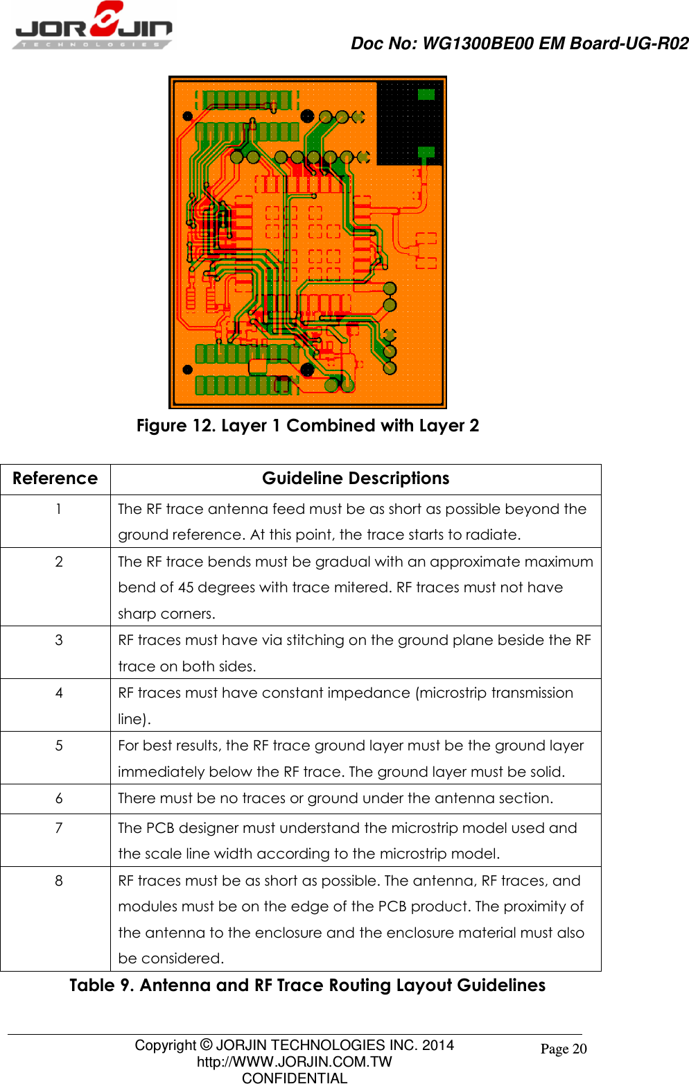
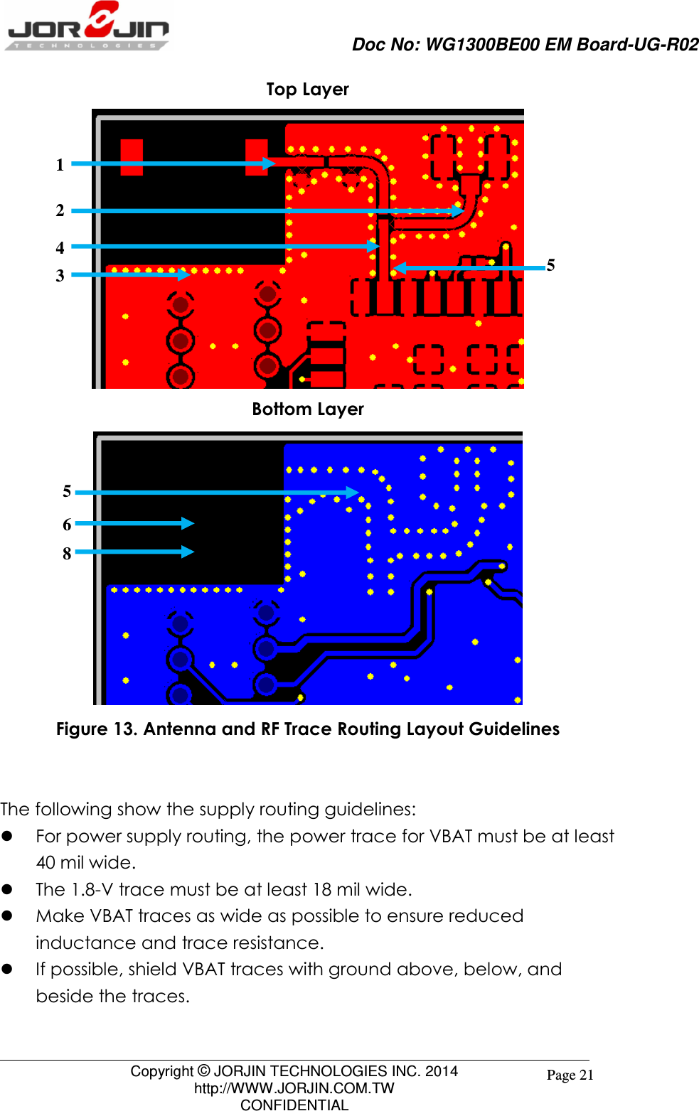
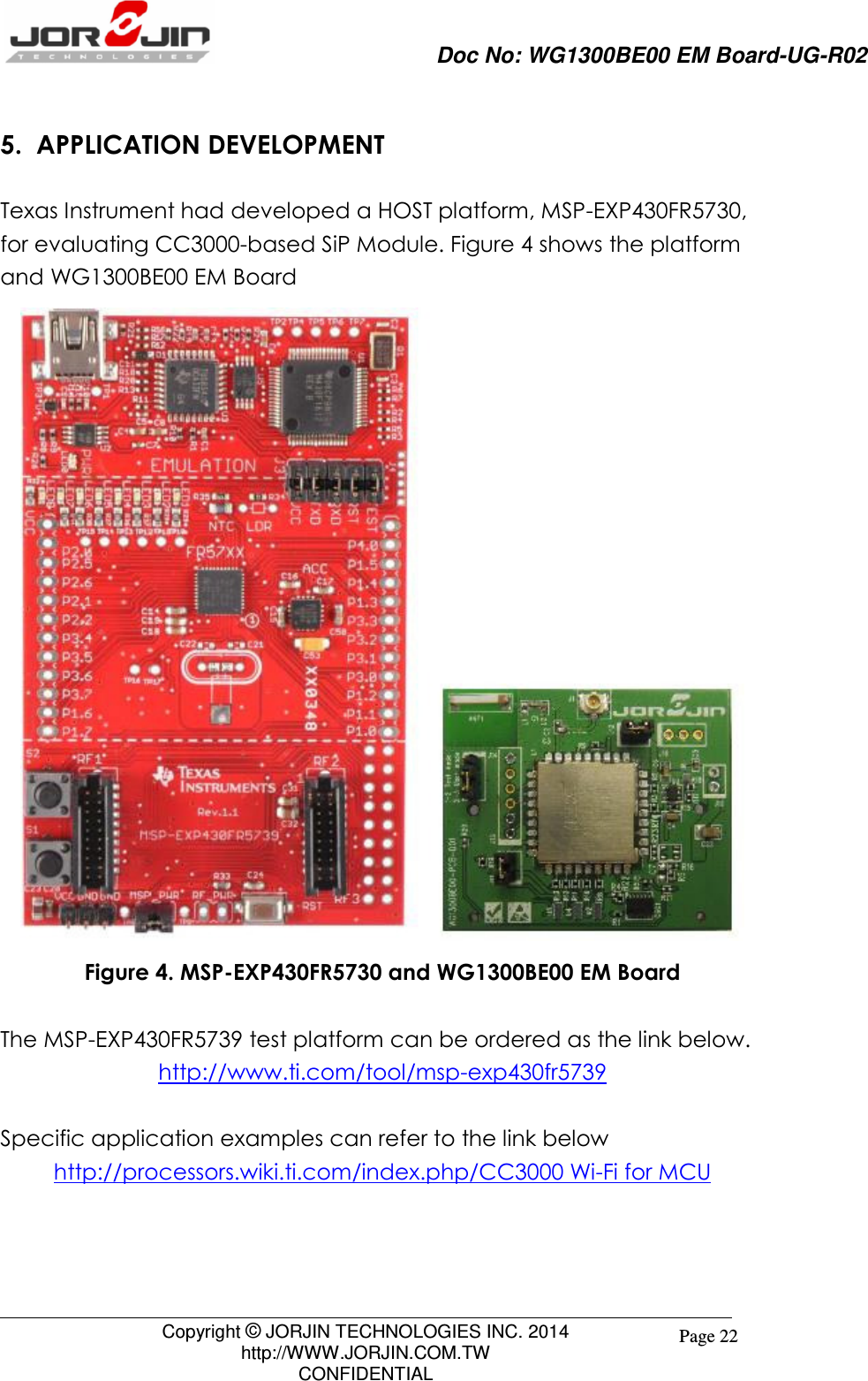
Jorjin Technologies WG1300B0 WIFI MODULE User Manual 1

Jorjin Technologies Inc. WIFI MODULE 1

User Manual

Copyright ©  JORJIN TECHNOLOGIES INC. 2013 http://WWW.JORJIN.COM.TW CONFIDENTIAL     a  module  solution  provider     WG1300-B0          Evaluation Module User Guide Revision 0.2
                    Doc No: WG1300BE00 EM Board-UG-R02                                                                                        Copyright © JORJIN TECHNOLOGIES INC. 2014 http://WWW.JORJIN.COM.TW CONFIDENTIAL Page 1 Index  0. REGULATION INFORMATION .......................................................................... 2 1. INTRODUCTION .................................................................................................... 7 2. WG1300-B0 EM BOARD ........................................................................................ 7 2.1. TOP SIDE ............................................................................................................. 7 2.2. BOTTOM SIDE .................................................................................................. 10 2.3. HARDWARE SETUP ............................................................................................. 12 2.4. SCHEMATICS ....................................................................................................... 13 2.5. BILL OF MATERIAL (BOM) ................................................................................ 14 3. ANTENNA CHARACTERISTICS ...................................................................... 15 3.1. RETURN LOSS & VSWR .................................................................................... 15 3.2. PLANE DEFINITION ............................................................................................. 15 3.3. 3D RADIO PATTERN ............................................................................................ 16 3.4. 2D RADIO PATTERN ............................................................................................ 17 4. LAYOUT GUIDELINES ....................................................................................... 18 4.1. BOARD LAYOUT ................................................................................................. 18 5. APPLICATION DEVELOPMENT ...................................................................... 22 6. HISTORY CHANGE ............................................................................................. 23
                    Doc No: WG1300BE00 EM Board-UG-R02                                                                                        Copyright © JORJIN TECHNOLOGIES INC. 2014 http://WWW.JORJIN.COM.TW CONFIDENTIAL Page 2 0.  REGULATION INFORMATION Federal Communication Commission Interference Statement This device complies with Part 15 of the FCC Rules. Operation is subject to the following two conditions: (1) This device may not cause harmful interference, and (2) this device must accept any interference received, including interference that may cause undesired operation. This equipment has been tested and found to comply with the limits for a Class B digital device, pursuant to Part 15 of the FCC Rules. These limits are designed to provide reasonable protection against harmful interference in a residential installation. This equipment generates, uses and can radiate radio frequency energy and, if not installed and used in accordance with the instructions, may cause harmful interference to radio communications. However, there is no guarantee that interference will not occur in a particular installation. If this equipment does cause harmful interference to radio or television reception, which can be determined by turning the equipment off and on, the user is encouraged to try to correct the interference by one of the following measures:  - Reorient or relocate the receiving antenna. - Increase the separation between the equipment and receiver. - Connect the equipment into an outlet on a circuit different from that to which the receiver is connected. - Consult the dealer or an experienced radio/TV technician for help.  FCC Caution: Any changes or modifications not expressly approved by the party responsible for compliance could void the user's authority to operate this equipment. This transmitter must not be co-located or operating in conjunction with any other antenna or transmitter.  Radiation Exposure Statement: This equipment complies with FCC radiation exposure limits set forth for an uncontrolled environment. This equipment should be installed and operated with minimum distance 20cm between the radiator & your body.
                    Doc No: WG1300BE00 EM Board-UG-R02                                                                                        Copyright © JORJIN TECHNOLOGIES INC. 2014 http://WWW.JORJIN.COM.TW CONFIDENTIAL Page 3 This device is intended only for OEM integrators under the following conditions:  1) The antenna must be installed such that 20 cm is maintained between the antenna and users, and 2) The transmitter module may not be co-located with any other transmitter or antenna. 3) The monopole chip antenna with 2.5 dBi gain was verified in the conformity testing. Radiated transmit power must be equal to or lower than that specified in the Equipment Authorization. A separate approval is required for all other antenna type, or higher gain antenna.  As long as 3 conditions above are met, further transmitter test will not be required. However, the OEM integrator is still responsible for testing their end-product for any additional compliance requirements required with this module installed  IMPORTANT NOTE: In the event that these conditions can not be met (for example certain laptop configurations or co-location with another transmitter), then the FCC authorization is no longer considered valid and the FCC ID can not be used on the final product. In these circumstances, the OEM integrator will be responsible for re-evaluating the end product (including the transmitter) and obtaining a separate FCC authorization.  End Product Labeling This transmitter module is authorized only for use in device where the antenna may be installed such that 20 cm may be maintained between the antenna and users. The final end product must be labeled in a visible area with the following: “Contains FCC ID: WS2-WG1300B0”. The grantee's FCC ID can be used only when all FCC compliance requirements are met.  Manual Information To the End User The OEM integrator has to be aware not to provide information to the end user regarding how to install or remove this RF module in the user’s manual of the end product which integrates this module. The end user manual shall include all required regulatory information/warning as show in this manual.
                    Doc No: WG1300BE00 EM Board-UG-R02                                                                                        Copyright © JORJIN TECHNOLOGIES INC. 2014 http://WWW.JORJIN.COM.TW CONFIDENTIAL Page 4 Industry Canada statement:  This device complies with RSS-210 of the Industry Canada Rules. Operation is subject to the following two conditions: (1) This device may not cause harmful interference, and (2) this device must accept any interference received, including interference that may cause undesired operation.  Ce dispositif est conforme à la norme CNR-210 d'Industrie Canada applicable aux appareils radio exempts de licence. Son fonctionnement est sujet aux deux conditions suivantes: (1) le dispositif ne doit pas produire de brouillage préjudiciable, et (2) ce dispositif doit accepter tout brouillage reçu, y compris un brouillage susceptible de provoquer un fonctionnement indésirable.  Radiation Exposure Statement: This equipment complies with IC radiation exposure limits set forth for an uncontrolled environment. This equipment should be installed and operated with minimum distance 20cm between the radiator & your body.  Déclaration d'exposition aux radiations: Cet équipement est conforme aux limites d'exposition aux rayonnements IC établies pour un environnement non contrôlé. Cet équipement doit être installé et utilisé avec un minimum de 20 cm de distance entre la source de rayonnement et votre corps.  This device is intended only for OEM integrators under the following conditions: (For module device use) 1) The antenna must be installed such that 20 cm is maintained between the antenna and users, and 2) The transmitter module may not be co-located with any other transmitter or antenna. As long as 2 conditions above are met, further transmitter test will not be required. However, the OEM integrator is still responsible for testing their end-product for any additional compliance requirements required with this module installed. 3) The monopole chip antenna with 2.5 dBi gain was verified in the conformity testing. Radiated transmit power must be equal to or lower than that specified in the Equipment Authorization. A separate approval is required for all other antenna type, or higher gain antenna.
                    Doc No: WG1300BE00 EM Board-UG-R02                                                                                        Copyright © JORJIN TECHNOLOGIES INC. 2014 http://WWW.JORJIN.COM.TW CONFIDENTIAL Page 5 IMPORTANT NOTE: In the event that these conditions can not be met (for example certain laptop configurations or co-location with another transmitter), then the Canada authorization is no longer considered valid and the IC ID can not be used on the final product. In these circumstances, the OEM integrator will be responsible for re-evaluating the end product (including the transmitter) and obtaining a separate Canada authorization.  NOTE IMPORTANTE: Dans le cas où ces conditions ne peuvent être satisfaites (par exemple pour certaines configurations d'ordinateur portable ou de certaines co-localisation avec un autre émetteur), l'autorisation du Canada n'est plus considéré comme valide et l'ID IC ne peut pas être utilisé sur le produit final. Dans ces circonstances, l'intégrateur OEM sera chargé de réévaluer le produit final (y compris l'émetteur) et l'obtention d'une autorisation distincte au Canada.  End Product Labeling This transmitter module is authorized only for use in device where the antenna may be installed such that 20 cm may be maintained between the antenna and users. The final end product must be labeled in a visible area with the following: “Contains IC: 10462A-WG1300B0”.  Plaque signalétique du produit final Ce module émetteur est autorisé uniquement pour une utilisation dans un dispositif où l'antenne peut être installée de telle sorte qu'une distance de 20cm peut être maintenue entre l'antenne et les utilisateurs. Le produit final doit être étiqueté dans un endroit visible avec l'inscription suivante: "Contient des IC: 10462A-WG1300B0".  Manual Information To the End User The OEM integrator has to be aware not to provide information to the end user regarding how to install or remove this RF module in the user’s manual of the end product which integrates this module. The end user manual shall include all required regulatory information/warning as show in this manual.  Manuel d'information à l'utilisateur final
                    Doc No: WG1300BE00 EM Board-UG-R02                                                                                        Copyright © JORJIN TECHNOLOGIES INC. 2014 http://WWW.JORJIN.COM.TW CONFIDENTIAL Page 6 L'intégrateur OEM doit être conscient de ne pas fournir des informations à l'utilisateur final quant à la façon d'installer ou de supprimer ce module RF dans le manuel de l'utilisateur du produit final qui intègre ce module. Le manuel de l'utilisateur final doit inclure toutes les informations réglementaires requises et avertissements comme indiqué dans ce manuel.  Under Industry Canada regulations, this radio transmitter may only operate using an antenna of a type and maximum (or lesser) gain approved for the transmitter by Industry Canada. To reduce potential radio interference to other users, the antenna type and its gain should be so chosen that the equivalent isotropically radiated power (e.i.r.p.) is not more than that necessary for successful communication.
                    Doc No: WG1300BE00 EM Board-UG-R02                                                                                        Copyright © JORJIN TECHNOLOGIES INC. 2014 http://WWW.JORJIN.COM.TW CONFIDENTIAL Page 7 1.  INTRODUCTION    The purpose of this user guide is to help user understanding how to use WG1300-B0 EM (Evaluation Module) board to complete hardware setup for test to evaluate the performances of CC3000 - WG1300-B0 SiP Module. 2.  WG1300-B0 EM BOARD   In the following sub-sections, it’ll divide into TOP and BOTTOM Side to explain details on the key parts and its features.   2.1.  TOP Side Figure 1 is TOP-Side picture of WG1300BE00 EM Board.  Figure 1. TOP Side of WG1300BE00 EM Board  The picture above marks some key parts and jumpers and Table 1 J10 J14 J16 J13 J1 Antenna CC3000-WG1300-B0 Module J11 J12
                    Doc No: WG1300BE00 EM Board-UG-R02                                                                                        Copyright © JORJIN TECHNOLOGIES INC. 2014 http://WWW.JORJIN.COM.TW CONFIDENTIAL Page 8 below shows the explanations to them in the details. Items Key Parts Descriptions 1 CC3000-WG1300-B0 Module The core module for performance evaluation. It’s related feature can be referred to its datasheet. 2 Antenna It can used for radiated test by reworking cpacitor to correct pads. 3 J1 It’s a U.FL RF connector via which you can proceed conducted power test. 4 J14 It is a jumper via which we can swap testing modes, test mode and operation mode. When pin 2 and pin 3 are shorted, it runs in operation mode and it operate in test mode when pin 1 and pin 2 are shorted. 5 J10 It is a jumper for testing power consumption. It is for the power for all circuit in this board. In operation mode, pins of the jumper is shorted. For power testing, the jumper is removed and ammeter crosses the pins to do the testing. 6 J12 It is a jumper for testing VBAT_IN power consumption of WG1300-B0. In operation mode, pins of the jumper is shorted. For power testing, the jumper is removed and ammeter crosses the pins to do the testing. 7 J11 It is a jumper for testing VIO_SOC power consumption of WG1300-B0. In operation mode, pins of the jumper is shorted. For power testing, the jumper is removed and ammeter crosses the pins to do the testing. 8 J13 Refer to Table 2. For more details on these through-hole test points   9 J16 Refer to Table 3. For more details on these through-hole test points Table 1. TOP-Side Key parts of WG1300BE00 EM Board
                    Doc No: WG1300BE00 EM Board-UG-R02                                                                                        Copyright © JORJIN TECHNOLOGIES INC. 2014 http://WWW.JORJIN.COM.TW CONFIDENTIAL Page 9 Table 2 below shows the signal descriptions of J13 Pin Number Pin Name Pin Type Descriptions 1 WL_RS232_RX I Test RS232 receive output; Leave floating for normal operation 2 WL_RS232_TX O Test RS232 transmit output; Leave floating for normal operation   3 WL_UART_DBG I/O UART Debug Line 4 NS_UARTD I/O Networking subsystem UART Debug line. 5 DC2DC_OUT P Internal DC2DC output power. 6 GND  Ground Table 2. TOP-Side J13 of WG1300BE00 EM Board  Table 3 below shows the signal descriptions of J16 Pin Number Pin Name Pin Type Descriptions 1 GND  Ground  2  SDA_EEPROM  I/O I2C Data signal from EEPROM inside CC3000-WG1300-B0 SiP Module. This pin is connected to SDA_CC3000 via a 0-Ohm resister and is not used by end users.  3  SCL_EEPROM  I I2C Clock signal input from EEPROM inside CC3000-WG1300-B0 SiP Module. This pin is connected to SCL_CC3000 via a 0-Ohm resister and is not used by end users. Table 3. TOP-Side J16 of WG1300BE00 EM Board
                    Doc No: WG1300BE00 EM Board-UG-R02                                                                                        Copyright © JORJIN TECHNOLOGIES INC. 2014 http://WWW.JORJIN.COM.TW CONFIDENTIAL Page 10 2.2.  BOTTOM Side Figure 2 is BOTTOM-Side picture of WG1300BE00 EM Board.  Figure 2. Bottom Side of WG1300BE00 EM Board  There are two EM Board mating connectors which are used for connecting to Host platform and mounted on the bottom side as the picture above. Table 4 and Table 5 show the descriptions on the signals brought out from these two EM mating connectors.  J6 Pin Number Pin Name Module Pin Type Description 1 GND  Ground  5  EXT_32KHz  I External Slow Clock input from Host device. It can be used for the SiP Module inside which hasn’t slow clock source. 10 VBAT_SW_EN I Active-high enable signal from Host device. 12 WL_SPI_IRQ O Host Interface SPI Interrupt Request J6 J7
                    Doc No: WG1300BE00 EM Board-UG-R02                                                                                        Copyright © JORJIN TECHNOLOGIES INC. 2014 http://WWW.JORJIN.COM.TW CONFIDENTIAL Page 11 14 WL_SPI_CS I Host interface SPI Chip Select 16 WL_SPI_CLK I Host interface SPI Clock input 18 WL_SPI_DIN I Host Interface SPI Data Input 19 GND  Ground 20 WL_SPI_DOUT O Host interface SPI Data Ouput Table 4. BOTTOM-Side J6 of WG1300BE00 EM Board  J7 Pin Number Pin Name Module Pin Type Description 2 GND  Ground 7 VBAT_IN PI Battery voltage input to Module 9 VBAT_IN PI Battery voltage input to Module 15 EXT_32KHz I External Slow Clock input from Host device. Table 5. BOTTOM-Side J7 of WG1300BE00 EM Board
                    Doc No: WG1300BE00 EM Board-UG-R02                                                                                        Copyright © JORJIN TECHNOLOGIES INC. 2014 http://WWW.JORJIN.COM.TW CONFIDENTIAL Page 12 2.3.  Hardware Setup Before conducting performance test, EM Board should be connected to Host platform with mating connectors, J6 and J7. For the case of using EM mating connector for hardware connection, the mating EM connector should be lined up and spaced 1.2” apart as Figure 3 below     Figure 3. Host PCB Mating Connector Arrangement
                    Doc No: WG1300BE00 EM Board-UG-R02                                                                                        Copyright © JORJIN TECHNOLOGIES INC. 2014 http://WWW.JORJIN.COM.TW CONFIDENTIAL Page 13 2.4.  Schematics Figure 4 is the schematics of WG1300E00 EM Board  C7NL_1uFCAP1608R16NL_100KRES1005WL_TXVBAT_SYSR6NL_0RRES1005To VIO_SYS Host LevelWL_DBGVBAT_SYSR19NL_10KRES1005VBAT_SYSU1WG1300-B0E_N51_14.5X14.5_1.3WL_UAR T_DBG2NS_UAR TD33WL_EN14WL_EN23WL_RS232_T X5WL_RS232_R X6EXT_32K 17GND36SCL_CC 3000 24SCL_EEPROM 23SDA_CC 3000 26SDA_EEPROM 25SPI_IR Q 13SPI_DOU T 12SPI_CS 15SPI_CLK 14SPI_DI N 11RF_AN T35DC2D C_OUT30GND 27GND1GND9GND37GND38GND39GND40GND 16VBAT_IN28GND31GND7VIO_SOC8GND 19GND34GND41GND42GND43GND 51GND 50GND 49GND 48GND 44GND 45GND 46GND 47XTALM 21XTALP 20GND 18GND29GND 10GND 22CLK_REQ_OU T32R23NL_0RRES1005VBAT_SYS: 2.7V~4.8V => 3.6V TYPVBAT_SYSVBAT_SW_ENVIO_SOC: 1.62V~1.92V => 1.8V TYPWL_RXWL_DBGWL_TXC3NL_10pFCAP1005J1U.F L-R-SMT(10)U.FL123L22.2nHIND 1005C12.2pFCAP1005L1NLIND 1005C210pFCAP1005WL_EN1ANT1AT8010-E2R9HAA8.0x1. 0x1.0mm12VIO_CLKThe Antenna matching circuit.VBAT_INVBAT_INU2SN74AVC2T45XBGA-N8_1X2_0. 5-AVCCA1A12A23GND4VCCB 8B1 7B2 6DIR 5VIO_SOCVIO LDONS_UAR TU4SN74AVC2T45XBGA-N8_1X2_0. 5-AVCCA1A12A23GND4VCCB 8B1 7B2 6DIR 5R17 0RRES1005WL_SPI_I RQ_1V8WL_SPI_D OUT_1V8U5SN74AVC2T45XBGA-N8_1X2_0. 5-AVCCA1A12A23GND4VCCB 8B1 7B2 6DIR 5WL_SPI_C S_1V8U6TPS22913BXBGA-N4_0.9x0.9_0. 5VINA2 VOUT A1ONB2 GND B1VBAT_INU3TPS79718MO-203_2.1x2GND2NC3IN 4OUT 5PG1R9 0R RES1005VIO_SYS: Voltage of Host LevelWL_SPI_I RQ_HOSTWL_SPI_D OUT_HOST-->C61uFCAP1608R18100KRES1005-->VIO_SOCC41uFCAP1608-->DIR High : A data to B busDIR Low : B data to A busVBAT_SYSR15100KRES1005VBAT_SYSC5 0.1uFCAP1005WL_SPI_C LK_HOSTWL_SPI_D IN_HOSTWL_SPI_C S_HOSTVBAT_SYS FET SWITCHWL_SPI_C LK_1V8WL_SPI_D IN_1V8WL_EN1DC2D C_OUTR30RRES1005J14Male 1x3123RTTT DebugVIO_SOCNetworking Subsystem DebugNS_UAR TDC2D C_OUTWL Debug LoggerR4NL_0RRES1005VBAT_INVIO_SOCR10RRES100532KHz_1V8_HOSTR7 NL_0RRES1005SLOW CLK 32.768KHzOSC1SG-3030LC/32. 768kHzCY -N12_3.6X2.8_0.5VIO 1VCC12OUT7GND 6NC 2NC 3NC 4NC 5NC8NC9NC10 NC11R20RRES1005J10Male 1x212Connect to Host SPI Interface.(Host I/O level: VIO_SYS)Internal Power FET Switch Enable.Connect to Host GPIO.VIO_SOCThe 32.768kHz clock select.Connect to OSC or Host source. J16NL_Male 1x3123R14NL_0RRES1005VIO_SOCC2210uFCAP2012J11Male 1x212Debug mode => 1-2 short to GNDFunctional mode => 2-3 shortWL_EN2VIO_SOCEM ConnectorJ12Male 1x212WL_SPI_C S_1V8R8 0R RES1005R11 0R RES1005 W L_SPI_IRQ_1V8R10 0R RES1005 W L_SPI_CLK_1V8R13 0R RES1005 W L_SPI_DIN_1V8R12 0R RES1005 W L_SPI_DOUT_1V8VBAT_SYSR21 NL_0RRES100532KHz_1V8_HOST32KHz_1V8_HOST R20 N L_0RRES1005WL_SPI_D IN_HOSTWL_SPI_C LK_HOSTVBAT_SW_ENWL_SPI_C S_HOSTWL_SPI_D OUT_HOSTWL_SPI_I RQ_HOSTJ6SFM-110-02-L-D-Apitch  1.27-2x101357911131517192468101214161820R50RRES1005VBAT_SYSJ7SFM-110-02-L-D-Apitch  1.27-2x101357911131517192468101214161820R220RRES1005J13Male 1x6123456VBAT_SYSVBAT_SYSVIO_CLK:  3.3VVBAT_INReserved VIO CLK LDOVIO_CLKWL_RXU7NL_TPS79733MO-203_2.1x2GND2NC3IN 4OUT 5PG1  Figure 4. Schematics of WG1300BE00 EM Board
                    Doc No: WG1300BE00 EM Board-UG-R02                                                                                        Copyright © JORJIN TECHNOLOGIES INC. 2014 http://WWW.JORJIN.COM.TW CONFIDENTIAL Page 14    2.5.  Bill Of Material (BOM) Table 6. BOM of WG1300BE00 EM Board  Items Reference Designator Description 1 U1 TI CC3000 WiFi b/g Module (LC) 2 U2, U4, U5 IC BUS TRANSCEIVER, SN74AVC2T45YZPR 3 U3 IC Regulator, TPS79718DCK 4 U6 IC Power Switch, TPS22913BYZV 5 OSC1 OSC 3225 / 32.768KHz / 1.5~5.5V / 5ppm 6 ANT1 ANT / 2.4GHZ / Peak Gain 2.5DB 7 J10, J11, J12 CON Male 1x2 / Pitch 2.0 mm 8 J14 CON Male 1x3 / Pitch 2.0 mm 9 J6,J7 Female Header / Fool Proof H:4.3 / 2x10 /   Pitch 1.27mm / SMT 10 J1 Mini RF Header Receptacle 11 R1, R2, R3, R5, R8, R9, R10, R11, R12, R13, R17, R22 RES 0402 / 0R / ±5% 12 R15, R18 RES 0402 / 100K / ±5% 13 L2 IND 0402 / 2.2nH / ±0.3nH / 0.16ohm / 300mA 14 C1 CAP 0402 / 2.2pF / 50V / NPO / ±0.25pF 15 C2 CAP 0402 / 10pF / 50V / NPO / ±5% 16 C5 CAP 0402 / 0.1uF / 10V / X7R / ±10% 17 C4, C6 CAP 0603 / 1uF / 16V / X7R / ±10% 18 C22 CAP 0805 / 10uF / 10V / X5R / ±10%
                    Doc No: WG1300BE00 EM Board-UG-R02                                                                                        Copyright © JORJIN TECHNOLOGIES INC. 2014 http://WWW.JORJIN.COM.TW CONFIDENTIAL Page 15 3.  ANTENNA CHARACTERISTICS 3.1.  Return Loss & VSWR  Figure 5. Antenna return loss & VSWR  3.2.  Plane Definition     Figure 6. Plane Definition Y Z X
                    Doc No: WG1300BE00 EM Board-UG-R02                                                                                        Copyright © JORJIN TECHNOLOGIES INC. 2014 http://WWW.JORJIN.COM.TW CONFIDENTIAL Page 16      3.3.  3D Radio Pattern  Figure 7. 3D Radio Pattern   XY-Plane Theta=90° XZ-Plane Phi=0° YZ-Plane Phi=90°
                    Doc No: WG1300BE00 EM Board-UG-R02                                                                                        Copyright © JORJIN TECHNOLOGIES INC. 2014 http://WWW.JORJIN.COM.TW CONFIDENTIAL Page 17 3.4.  2D Radio Pattern   Figure 8. 2D Radio Pattern   Table 7. Gain Table  XY-Plane XZ-Plane YZ-Plane Efficiency Peak Avg. Peak Avg. Peak Avg. 0.3 -2.6 1.3 -4.2 0.9 -0.9 66.7%
                    Doc No: WG1300BE00 EM Board-UG-R02                                                                                        Copyright © JORJIN TECHNOLOGIES INC. 2014 http://WWW.JORJIN.COM.TW CONFIDENTIAL Page 18 4.  LAYOUT GUIDELINES 4.1.  Board Layout Figure 9 shows the 2 layers evaluation board.     Figure 9. Board Layout   Table 8 and Figure 10 describe instances of good layout practices.  Reference Guideline Descriptions 1 The proximity of ground vias must be close to the pad. 2  Signal traces must not be run underneath the module on the layer where the module is mounted. 3 Increase the ground pour in the first layer. 4 Have a solid ground plane and ground vias under the module for stable system and thermal dissipation. Table 8. Module Layout Guidelines
                    Doc No: WG1300BE00 EM Board-UG-R02                                                                                        Copyright © JORJIN TECHNOLOGIES INC. 2014 http://WWW.JORJIN.COM.TW CONFIDENTIAL Page 19  Figure 10. Module Layout Guidelines  Figure 11 shows the RF trace design for the PCB. A 50-Ω impedance match on the trace to the antenna should be used. Also, 50-Ω traces are recommended for the PCB layout. Figure 11 also lists the distances. Figure 12 shows layer 1 with the trace to the antenna over the layer 2. Table 9 and Figure 13 describe instances of good layout practices for the antenna and RF trace routing.     Figure 11. Trace Design for the PCB layout  1 2, 3 4
                    Doc No: WG1300BE00 EM Board-UG-R02                                                                                        Copyright © JORJIN TECHNOLOGIES INC. 2014 http://WWW.JORJIN.COM.TW CONFIDENTIAL Page 20  Figure 12. Layer 1 Combined with Layer 2  Reference Guideline Descriptions 1 The RF trace antenna feed must be as short as possible beyond the ground reference. At this point, the trace starts to radiate. 2  The RF trace bends must be gradual with an approximate maximum bend of 45 degrees with trace mitered. RF traces must not have sharp corners. 3 RF traces must have via stitching on the ground plane beside the RF trace on both sides. 4 RF traces must have constant impedance (microstrip transmission line). 5 For best results, the RF trace ground layer must be the ground layer immediately below the RF trace. The ground layer must be solid. 6 There must be no traces or ground under the antenna section. 7 The PCB designer must understand the microstrip model used and the scale line width according to the microstrip model. 8 RF traces must be as short as possible. The antenna, RF traces, and modules must be on the edge of the PCB product. The proximity of the antenna to the enclosure and the enclosure material must also be considered. Table 9. Antenna and RF Trace Routing Layout Guidelines
                    Doc No: WG1300BE00 EM Board-UG-R02                                                                                        Copyright © JORJIN TECHNOLOGIES INC. 2014 http://WWW.JORJIN.COM.TW CONFIDENTIAL Page 21 Top Layer  Bottom Layer  Figure 13. Antenna and RF Trace Routing Layout Guidelines   The following show the supply routing guidelines:  For power supply routing, the power trace for VBAT must be at least 40 mil wide.  The 1.8-V trace must be at least 18 mil wide.  Make VBAT traces as wide as possible to ensure reduced inductance and trace resistance.  If possible, shield VBAT traces with ground above, below, and beside the traces.  1 2 3 4 5 5 6 8
                    Doc No: WG1300BE00 EM Board-UG-R02                                                                                        Copyright © JORJIN TECHNOLOGIES INC. 2014 http://WWW.JORJIN.COM.TW CONFIDENTIAL Page 22 5.  APPLICATION DEVELOPMENT Texas Instrument had developed a HOST platform, MSP-EXP430FR5730, for evaluating CC3000-based SiP Module. Figure 4 shows the platform and WG1300BE00 EM Board  Figure 4. MSP-EXP430FR5730 and WG1300BE00 EM Board  The MSP-EXP430FR5739 test platform can be ordered as the link below. http://www.ti.com/tool/msp-exp430fr5739  Specific application examples can refer to the link below http://processors.wiki.ti.com/index.php/CC3000 Wi-Fi for MCU
                    Doc No: WG1300BE00 EM Board-UG-R02                                                                                        Copyright © JORJIN TECHNOLOGIES INC. 2014 http://WWW.JORJIN.COM.TW CONFIDENTIAL Page 23 6.  HISTORY CHANGE Revision Date Description R 0.1 2013/7/22 Release 0.1 R 0.2 2014/May/22 Add   3. Antenna Characteristics 4. Layout Guidelines

Navigation menu