Jorjin Technologies WG6031 WLAN module User Manual 1
Jorjin Technologies Inc. WLAN module 1
Users Manual

Copyright © JORJIN TECHNOLOGIES INC. 2017
http://WWW.JORJIN.COM.TW
CONFIDENTIAL
a module solution provider
WG6031-00 WLAN Module
Realtek RTL8189EM IEEE 802.11b/g/n
1T/1R Solution with SDIO/SPI Interface
Datasheet
Draft 0.2
Prepared By
Reviewed By
Approved By

Doc No: WG6031-00-DTS-D02
Copyright © JORJIN TECHNOLOGIES INC. 2017
http://WWW.JORJIN.COM.TW
CONFIDENTIAL
Page 1
Index
1. HISTORY CHANGE .............................................................................................................................. 2
2. GENERAL DESCRIPTION ..................................................................................................................... 3
2.1. FEATURES ........................................................................................................................................ 3
3. MODULE BLOCK DIAGRAM ............................................................................................................... 4
4. MODULE OUTLINE ............................................................................................................................. 5
4.1. SIGNAL LAYOUT (TOP VIEW) ............................................................................................................... 5
4.2. PIN DESCRIPTION ............................................................................................................................. 6
5. MODULE SPECIFICATION ................................................................................................................... 7
5.1. GENERAL MODULE REQUIREMENTS AND OPERATION .............................................................................. 7
5.1.1. Temperature Limit Ratings ................................................................................................... 7
5.1.2. DC Power Supply Characteristics .......................................................................................... 7
5.1.3. Digital IO DC Characteristics ................................................................................................ 7
5.2. WLAN RF PERFORMANCE ................................................................................................................. 8
5.2.1. WLAN 2.4-GHz Receiver Characteristics .............................................................................. 8
5.2.2. WLAN 2.4-GHz Transmitter Power ....................................................................................... 8
6. REFERENCE SCHEMATICS ................................................................................................................... 9
7. PACKAGE INFORMATION ................................................................................................................. 10
7.1. MODULE MECHANICAL OUTLINE ........................................................................................................ 10
7.2. ORDERING INFORMATION ............................................................................................................ 11
7.3. MODULE MARKING ..................................................................................................................... 11
7.4. CERTIFICATION INFORMATION ............................................................................................................ 11
8. SMT AND BAKING RECOMMENDATION ......................................................................................... 12
8.1. BAKING RECOMMENDATION ............................................................................................................. 12
8.2. SMT RECOMMENDATION ................................................................................................................ 12
9. REGULATORY INFORMATION .......................................................................................................... 14
9.1. UNITED STATES .............................................................................................................................. 14

Doc No: WG6031-00-DTS-D02
Copyright © JORJIN TECHNOLOGIES INC. 2017
http://WWW.JORJIN.COM.TW
CONFIDENTIAL
Page 2
1. HISTORY CHANGE
Revision
Date
Description
Draft 0.1
2017-06-05
Initial Document creation.
Draft 0.2
2017-10-06
1. Updated SDIO information.
2. Corrected RF Performance.
3. Updated Module Size tolerance.
4. Added Module Package Marking and Regulatory
Information.

Doc No: WG6031-00-DTS-D02
Copyright © JORJIN TECHNOLOGIES INC. 2017
http://WWW.JORJIN.COM.TW
CONFIDENTIAL
Page 3
2. GENERAL DESCRIPTION
The WG6031-00 is a 802.11b/g/n 1T1R Wireless LAN SiP (system in package) module with
SDIO/SPI interface. The WG6031-00 provides a complete solution for a high throughput
performance integrated wireless LAN device.
2.1. Features
Dimension 13mm(L) x 13mm(W) x 2.35mm(H).
LGA-20 pin package.
CMOS MAC, Baseband PHY, and RF in a single chip for 802.11b/g/n compatible WLAN.
Complete 802.11n solution for 2.4GHz band.
72.2Mbps receive PHY rate and 72.2Mbps transmit PHY rate using 20MHz bandwidth.
150Mbps receive PHY rate and 150Mbps transmit PHY rate using 40MHz bandwidth.
Compatible with 802.11n specification.
Backward compatible with 802.11b/g device while operating in 802.11n mode.
Operating temperature: 0°C to 70°C
Doc No: WG6031-00-DTS-D02
Copyright © JORJIN TECHNOLOGIES INC. 2017
http://WWW.JORJIN.COM.TW
CONFIDENTIAL
Page 4
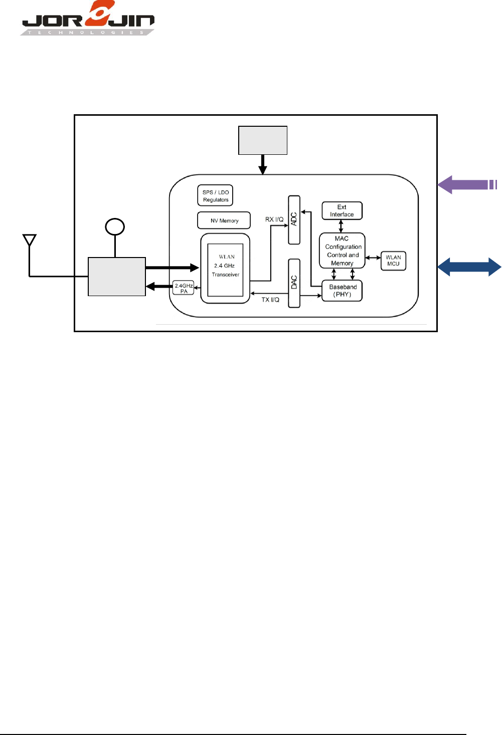
3. MODULE BLOCK DIAGRAM
Figure 3-1. WG6031-00 Block Diagram
RTL8189EM
Xtal
40MHz
TX/RX
Matching
Circuit
Internal
RF Connector
External
RF Design
(Default)
SDIO/SPI
Interface
VDD33
Doc No: WG6031-00-DTS-D02
Copyright © JORJIN TECHNOLOGIES INC. 2017
http://WWW.JORJIN.COM.TW
CONFIDENTIAL
Page 5
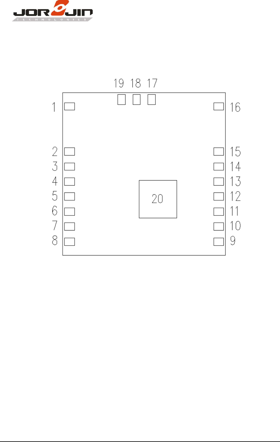
4. MODULE OUTLINE
4.1. Signal Layout (Top View)
Figure 4-1 Device pins (Top View)

Doc No: WG6031-00-DTS-D02
Copyright © JORJIN TECHNOLOGIES INC. 2017
http://WWW.JORJIN.COM.TW
CONFIDENTIAL
Page 6
4.2. Pin Description
Pin
Signal Name
Type
Description
1
GND
Power
Ground
2
GND
Power
Ground
3
GND
Power
Ground
4
NC (1)
I/O
SPI not Connection / SDIO D3
5
SPI_IRQ
O
SPI Interrupt Output / SDIO D2
6
SPI_SS
I
SPI Slave Select / SDIO D1
7
SPI_MISO
O
SPI Master in Slave out / SDIO D0
8
SPI_MOSI
I
SPI Master out Slave in / SDIO Command Input
9
SPI_CLK
I
SPI Clock Input / SDIO Clock Input
10
RESET
I
Hardware Reset
11
WAKE
I/O
General Purpose Input / Output Pin
12
GND
Power
Ground
13
VDD
Power
Power supply input. Typical 3.3V.
14
VDD
Power
Power supply input. Typical 3.3V.
15
GND
Power
Ground.
16
GND
Power
Ground.
17
GND
Power
Ground.
18
RF_OUT
RF
WLAN 2.4GHz External RF port.
19
GND
Power
Ground.
20
PGND
Power
Ground. Module Thermal PAD.
(1) SPI interface: this pin is no used. / SDIO interface: this pin is defined SDIO_D3.
Doc No: WG6031-00-DTS-D02
Copyright © JORJIN TECHNOLOGIES INC. 2017
http://WWW.JORJIN.COM.TW
CONFIDENTIAL
Page 7
5. MODULE SPECIFICATION
5.1. General Module Requirements and Operation
5.1.1. Temperature Limit Ratings
Parameter
Min
Max
Units
Storage Temperature
-40
+125
℃
Ambient Operating
0
+70
℃
5.1.2. DC Power Supply Characteristics
Parameter
Condition
Min
Typical
Max
Units
VDD
DC supply Voltage
3.0
3.3
3.6
V
5.1.3. Digital IO DC Characteristics
Parameter
Condition
Min
Normal
Max
Units
VIH
Input high voltage
2.0
3.3
3.6
V
VIL
Input low voltage
-
0
0.9
V
VOH
Output high voltage
2.97
-
3.3
V
VOL
Output low voltage
0
-
0.33
V
Doc No: WG6031-00-DTS-D02
Copyright © JORJIN TECHNOLOGIES INC. 2017
http://WWW.JORJIN.COM.TW
CONFIDENTIAL
Page 8
5.2. WLAN RF Performance
5.2.1. WLAN 2.4-GHz Receiver Characteristics
Parameter
Condition
Min
Typ
Max
Units
Operation frequency range
2412
2484
MHz
Sensitivity
At < 8% PER limit
1 Mbps DSSS
-95
dBm
11 Mbps CCK
-86
At < 10% PER At
< 10% PER limit
6 Mbps OFDM
-91
54 Mbps OFDM
-74
MCS0 MM
-90
MCS7 MM
-71
MCS0 MM 40MHz
-87
MCS7 MM 40MHz
-68
5.2.2. WLAN 2.4-GHz Transmitter Power
Parameter
Condition
Min
Typ
Max
Output Power
11 Mbps CCK
17
–
dBm
54 Mbps OFDM
15
–
MCS7 MM
14
–
MCS7 MM 40MHz
14
–
Frequency Accuracy
-20
+20
ppm
Doc No: WG6031-00-DTS-D02
Copyright © JORJIN TECHNOLOGIES INC. 2017
http://WWW.JORJIN.COM.TW
CONFIDENTIAL
Page 9
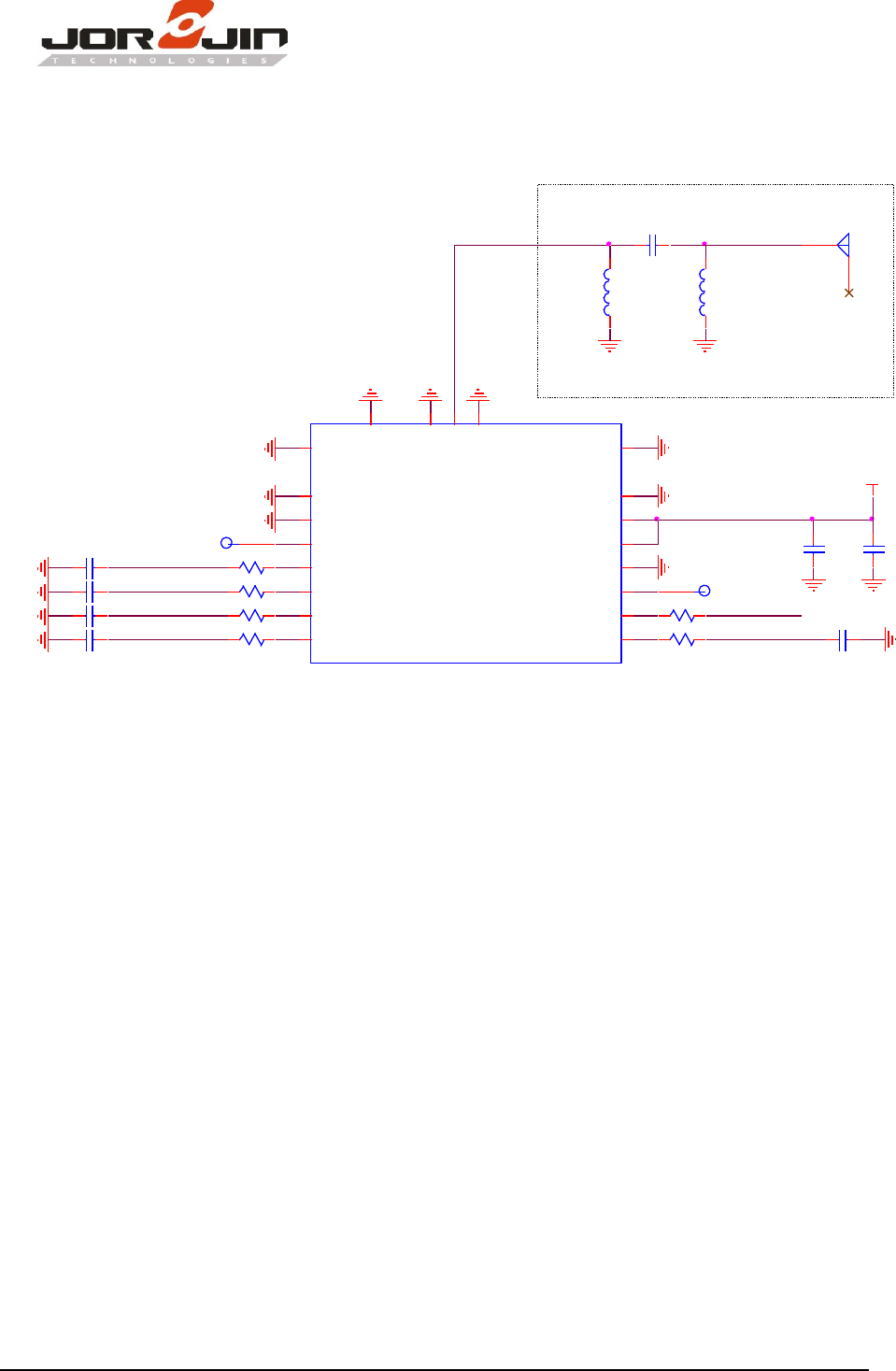
6. REFERENCE SCHEMATICS
TP2
1
R4 0R
0402 RESET
VDD33
C1
0.1uF
0402
C2
10uF
0603R1 0R
0402
R2 0R
0402
R3 0R
0402
SPI_IRQ
C3 NU
0402
SPI_MISO
SPI_SS
C4 NU
0402
C5 NU
0402
TP1 1
R6 0R
0402 C7 NU
0402
SPI_CLK
R5 0R
0402
SPI_MOSI
C6 NU
0402
RF_OUT
L1
NL
IND1005
C8
10pF
CAP1005
L2
NL
IND1005
ANT1
1
2
Pi-Circuit for Antenna matching.
U1
WG6031-00 Module
E-13X13-N20-1.2-TOP
3.3V 14
GND 17
RF OUT 18
GND 19
RESET 10
WAKE 11
SPI_IRQ/SD_D2
5
NC/SD_D3
4
SPI_MOSI/SD_CMD
8SPI_CLK/SD_CLK 9
SPI_MISO/SD_D0
7
SPI_SS/SD_D1
6
GND 12
3.3V 13
PGND 20
GND 15
GND 16
GND
3
GND
1
GND
2
PIN-4 defined as SDIO_D3
if SDIO interface.
Doc No: WG6031-00-DTS-D02
Copyright © JORJIN TECHNOLOGIES INC. 2017
http://WWW.JORJIN.COM.TW
CONFIDENTIAL
Page 10
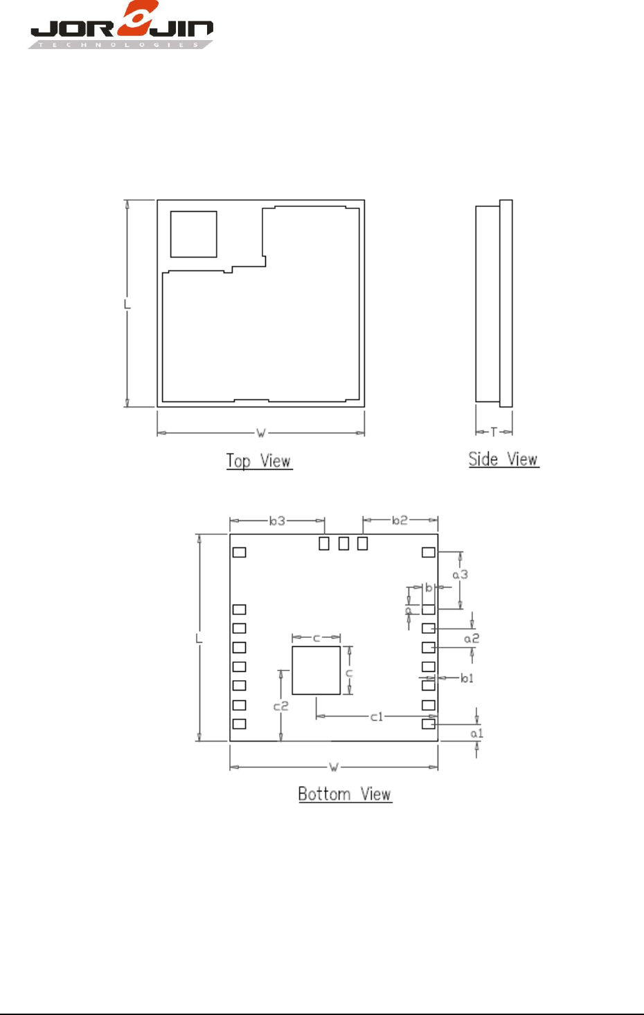
7. PACKAGE INFORMATION
7.1. Module mechanical outline
Figure 6-1 Module Pad Dimensions
Doc No: WG6031-00-DTS-D02
Copyright © JORJIN TECHNOLOGIES INC. 2017
http://WWW.JORJIN.COM.TW
CONFIDENTIAL
Page 11
Marking Min Nom Max Marking Min Nom Max
L (Body size) 12.85 13.00 13.15 b 0.75 0.80 0.85
W (Body size) 12.85 13.00 13.15 b1 0.10 0.15 0.20
T (Thickness) 2.15 2.35 2.55 b2 4.65 4.70 4.75
a 0.55 0.60 0.65 b3 5.85 5.90 5.95
a1 1.05 1.10 1.15 c 2.95 3.00 3.05
a2 1.15 1.20 1.25 c1 7.55 7.60 7.65
a3 3.55 3.60 3.65 c2 4.45 4.50 4.55
Table 7-1. Dimensions for Module Mechanical Outline
7.2. Ordering Information
Part number:
WG6031-00A
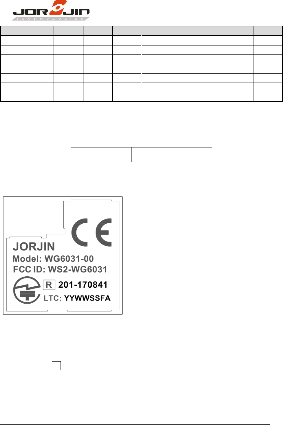
7.3. Module Marking
LTC : Date Code , YYWWSSFA
YY = Digit of the year, ex: 2017=17
WW = Week (01~52)
SS = Serial number from 01 ~99 match to
manufacture’s lot number.
F = Reserve for internal use.
A = Module version.
7.4. Certification Information
FCC : WS2-WG6031, FCC grant ID
TELEC : R 201-170841, TELEC grant ID and compliance mark
CE : CE compliance mark
Doc No: WG6031-00-DTS-D02
Copyright © JORJIN TECHNOLOGIES INC. 2017
http://WWW.JORJIN.COM.TW
CONFIDENTIAL
Page 12
8. SMT AND BAKING RECOMMENDATION
8.1. Baking Recommendation
Baking condition:
- Follow MSL Level 4 to do baking process.
- After bag is opened, devices that will be subjected to reflow solder or other high
temperature process must be
a) Mounted within 72 hours of factory conditions <30°C/60% RH, or
b) Stored at <10% RH.
- Devices require bake, before mounting, if Humidity Indicator Card reads >10%
If baking is required, Devices may be baked for 8 hrs at 125 °C.
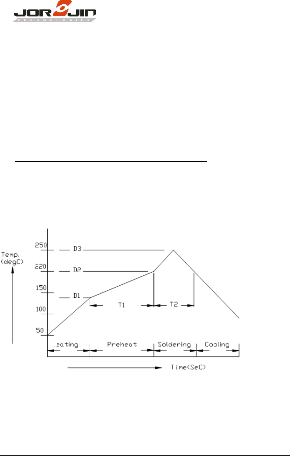
8.2. SMT Recommendation
Recommended Reflow profile:
H

Doc No: WG6031-00-DTS-D02
Copyright © JORJIN TECHNOLOGIES INC. 2017
http://WWW.JORJIN.COM.TW
CONFIDENTIAL
Page 13
No.
Item
Temperature (°C)
Time (sec)
1
Pre-heat
D1: 140 ~ D2: 200
T1: 80 ~ 120
2
Soldering
D2: = 220
T2: 60 ± 10
3
Peak-Temp.
D3: 250 °C max
Note: (1) Reflow soldering is recommended two times maximum.
(1) Add Nitrogen while Reflow process: SMT solder ability will be better.
Stencil thickness: 0.1~ 0.15 mm (Recommended)
Soldering paste (without Pb): Recommended SENJU N705-GRN3360-K2-V can get better
soldering effects.

Doc No: WG6031-00-DTS-D02
Copyright © JORJIN TECHNOLOGIES INC. 2017
http://WWW.JORJIN.COM.TW
CONFIDENTIAL
Page 14
9. REGULATORY INFORMATION
This section outlines the regulatory information for the following countries:
United States
Europe
Japan
9.1. United States
Federal Communications Commission Statement
This equipment has been tested and found to comply with the limits for a Class B digital device,
pursuant to Part 15 of the FCC Rules. These limits are designed to provide reasonable protection
against harmful interference in a residential installation. This equipment generates, uses and can
radiate radio frequency energy and, if not installed and used in accordance with the instructions,
may cause harmful interference to radio communications. However, there is no guarantee that
interference will not occur in a particular installation. If this equipment does cause harmful
interference to radio or television reception, which can be determined by turning the equipment off
and on, the user is encouraged to try to correct the interference by one of the following measures:
- Reorient or relocate the receiving antenna.
- Increase the separation between the equipment and receiver.
- Connect the equipment into an outlet on a circuit different from that to which the receiver is
connected.
- Consult the dealer or an experienced radio/TV technician for help.
FCC Caution:
Any changes or modifications not expressly approved by the party responsible for compliance
could void the user's authority to operate this equipment.
This device complies with Part 15 of the FCC Rules. Operation is subject to the following two
conditions:
(1) This device may not cause harmful interference, and
(2) This device must accept any interference received, including interference that may cause
undesired operation.

Doc No: WG6031-00-DTS-D02
Copyright © JORJIN TECHNOLOGIES INC. 2017
http://WWW.JORJIN.COM.TW
CONFIDENTIAL
Page 15
FCC RF Radiation Exposure Statement:
This device complies with FCC radiation exposure limits set forth for an uncontrolled
environment and it also complies with Part 15 of the FCC RF Rules.
This device is intended only for OEM integrators under the following conditions:
(1) The antenna must be installed such that 20cm is maintained between the antenna and users,
and
(2) The transmitter module may not be co-located with any other transmitter or antenna,
(3) For all products market in US, OEM has to limit the operation channels in CH1 to CH11 for
2.4Gband by supplied firmware programming tool. OEM shall not supply any tool or info to the
end-user regarding to Regulatory Domain change.
As long as 3 conditions above are met, further transmitter test will not be required. However,
the OEM integrator is still responsible for testing their end-product for any additional compliance
requirements required with this module installed.
Important Note:
In the event that these conditions cannot be met (for example certain laptop configurations or
co-location with another transmitter), then the FCC authorization is no longer considered valid and
the FCC ID cannot be used on the final product. In these circumstances, the OEM integrator will be
responsible for re-evaluating the end product (including the transmitter) and obtaining a separate
FCC authorization.
End Product Labeling:
The final end product must be labelled in a visible area with the following:
“Contains FCC ID: WS2-WG6031”.
Manual Information to the End User
The OEM integrator has to be aware not to provide information to the end user regarding how
to install or remove this RF module in the user’s manual of the end product which integrates this
module.