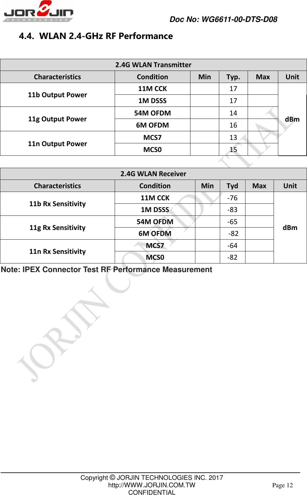
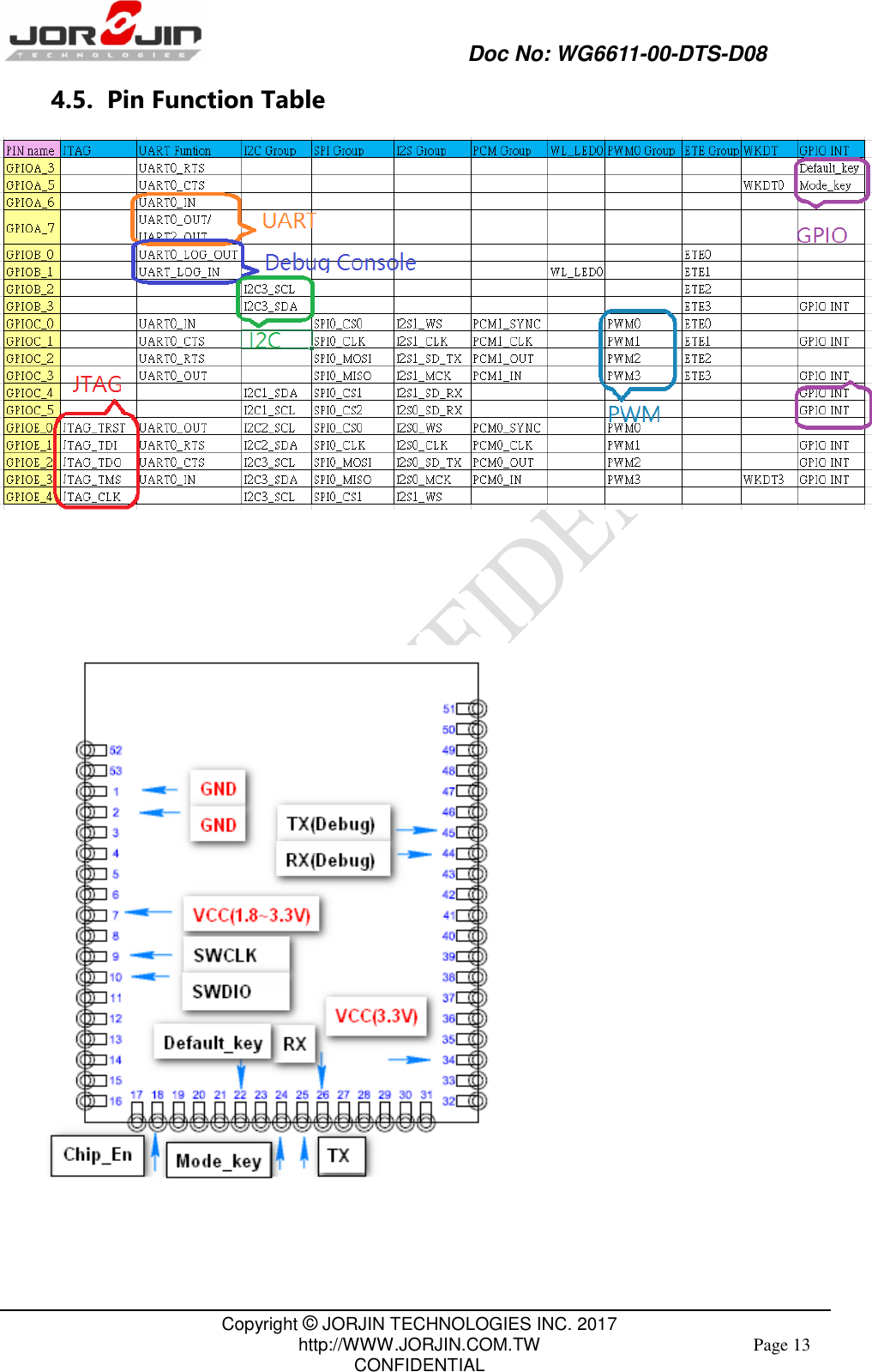
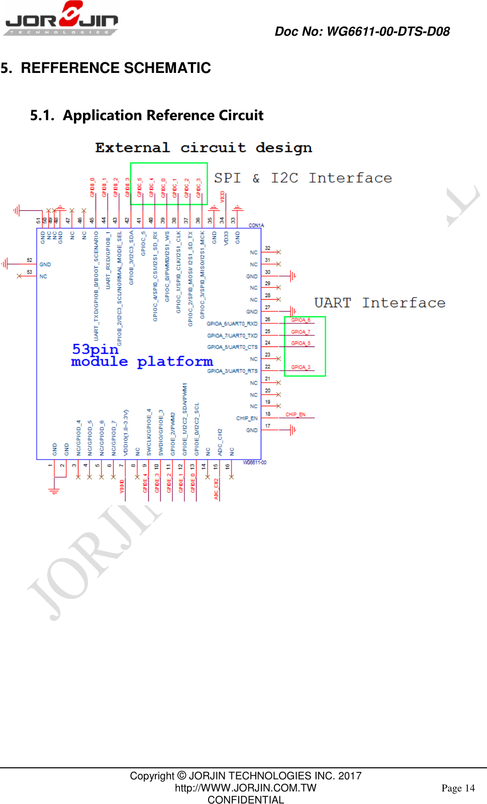
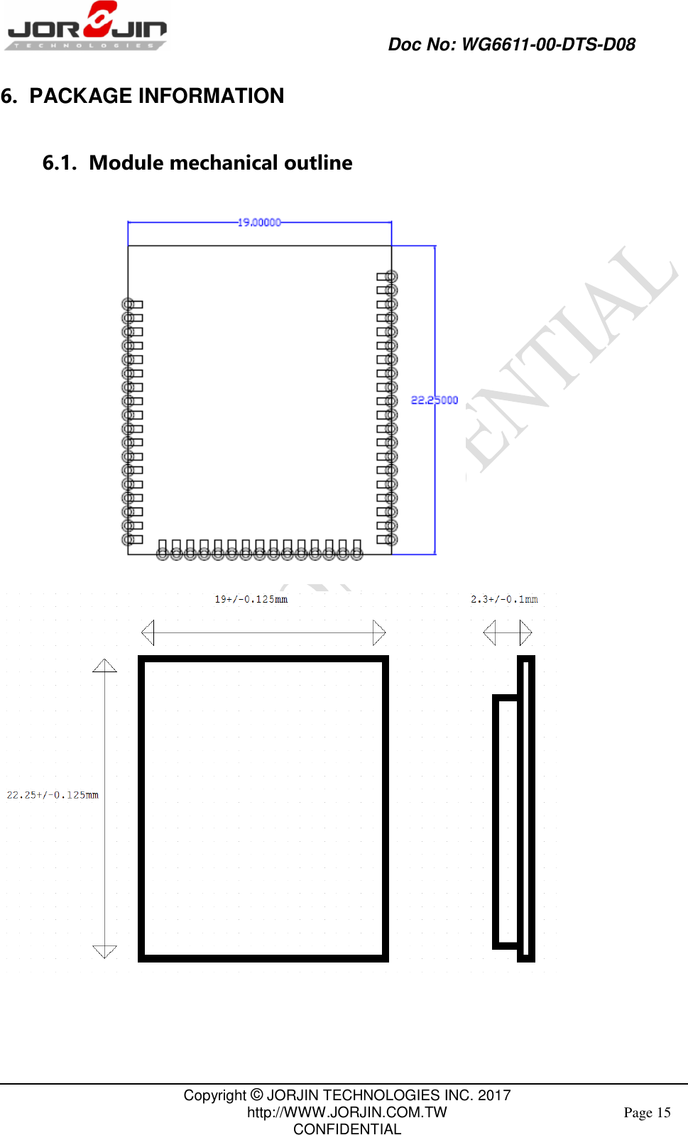
Jorjin Technologies WG6611 WLAN module User Manual 1
Jorjin Technologies Inc. WLAN module 1
UserManual.wiki
>
Jorjin Technologies
>
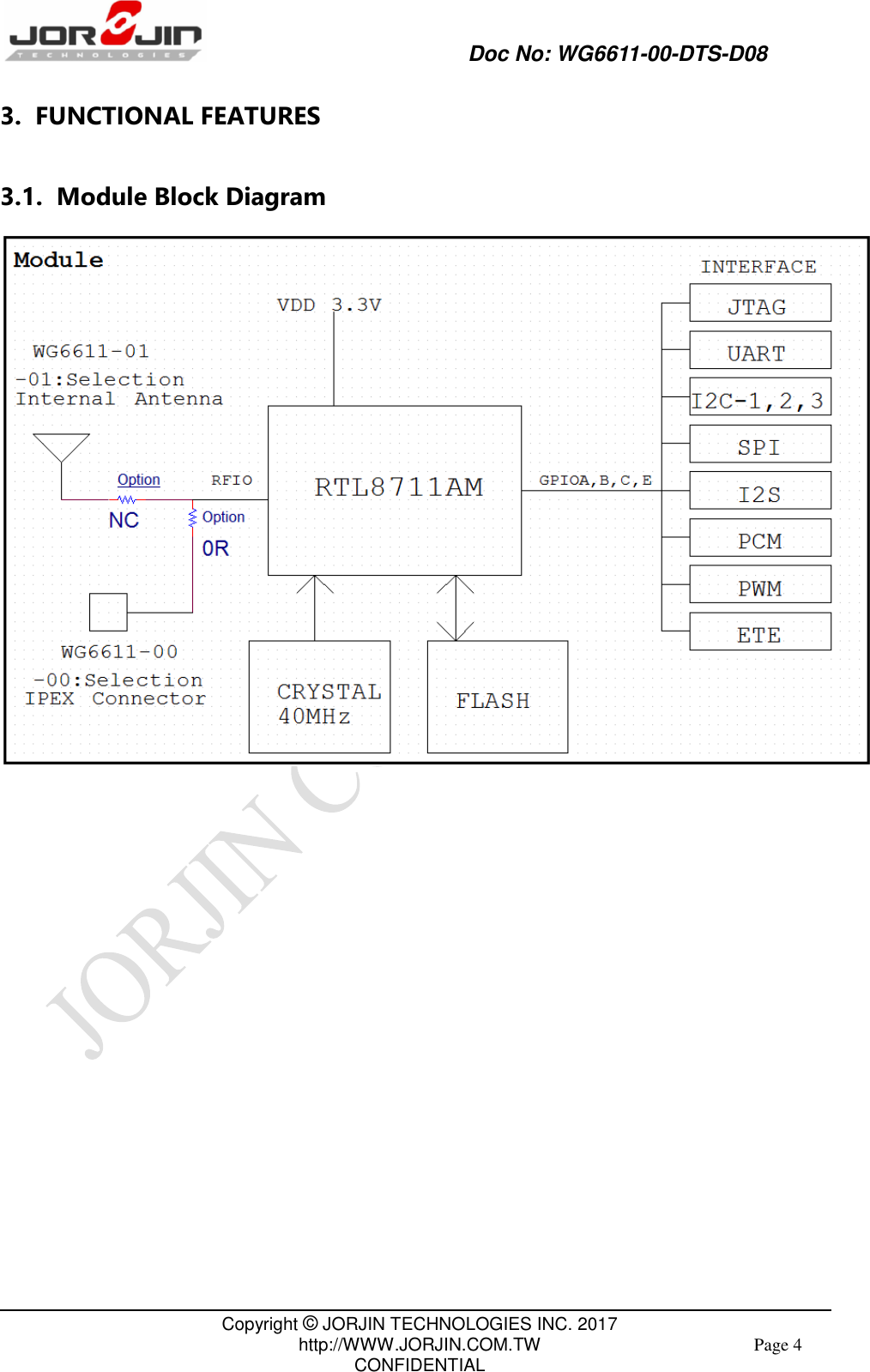
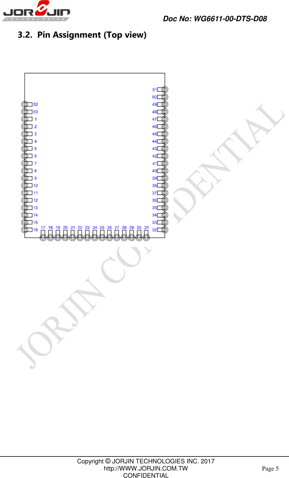
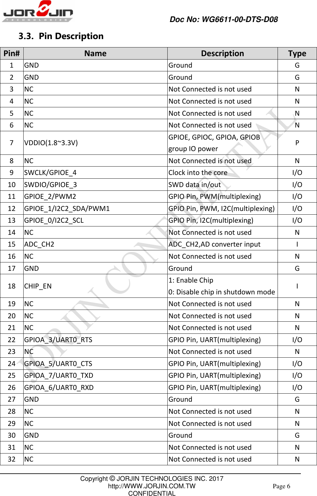
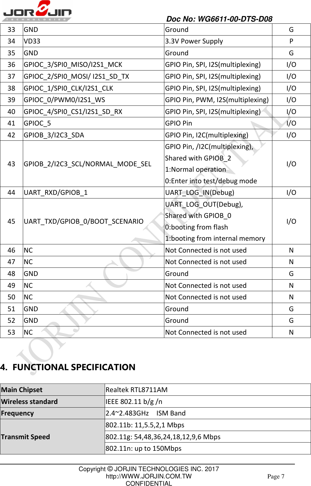
WG6611 User Manual
Users Manual
Navigation menu
Upload a User Manual
Namespaces
Wiki Guide
HTML
PDF
Info
Views
User Manual
Discussion / Help
Navigation