Jorjin Technologies WG6611 WLAN module User Manual 1
Jorjin Technologies Inc. WLAN module 1
Users Manual

Doc No: WG6611-00-DTS-D08
Copyright © JORJIN TECHNOLOGIES INC. 2017
http://WWW.JORJIN.COM.TW
CONFIDENTIAL
Page 1
Index
1. HISTORY CHANGE ....................................................................................................................... 2
2. GENERAL DESCRIPTION ........................................................................................................... 3
3. FUNCTIONAL FEATURES ........................................................................................................... 4
3.1. MODULE BLOCK DIAGRAM .......................................................................................................... 4
3.2. PIN ASSIGNMENT (TOP VIEW) ....................................................................................................... 5
3.3. PIN DESCRIPTION ......................................................................................................................... 6
4. FUNCTIONAL SPECIFICATION ................................................................................................ 7
4.1. TEMPERATURE LIMIT RATINGS ................................................................................................... 10
4.2. DC POWER SUPPLY ............................................................................................................... 10
4.3. CURRENT CONSUMPTION ............................................................................................................ 11
4.4. WLAN 2.4-GHZ RF PERFORMANCE .......................................................................................... 12
4.5. PIN FUNCTION TABLE ................................................................................................................. 13
5. REFFERENCE SCHEMATIC ...................................................................................................... 14
5.1. APPLICATION REFERENCE CIRCUIT ............................................................................................ 14
6. PACKAGE INFORMATION ......................................................................................................... 15
6.1. MODULE MECHANICAL OUTLINE ................................................................................................ 15
6.2. PACKAGE MARKING ................................................................................................................... 17
7. SMT AND BAKING RECOMMENDATION ............................................................................. 18
7.1. BAKING RECOMMENDATION ...................................................................................................... 18
7.2. SMT RECOMMENDATION ........................................................................................................... 18
Doc No: WG6611-00-DTS-D08
Copyright © JORJIN TECHNOLOGIES INC. 2017
http://WWW.JORJIN.COM.TW
CONFIDENTIAL
Page 2
1. HISTORY CHANGE
Revision
Date
Description
D0.1
2016-01-13
Initial Document creation.
D0.2
2016-02-26
Verify Current Consumption
D0.3
2016-03-08
Verify Application Reference Circuit
D0.4
2016-03-17
Modify Functional Specification remove
Certification
D0.5
2016-06-21
1. Modify Functional Specification increased
IPEX Connector
2. Cover modify Series Specifications
3. Modify Module Block Diagram
D0.6
2016-09-20
1. Modify Application Reference Circuit
2. Modify pin Description
3. Modify Module Block Diagram
D0.7
2016-10-13
1. Remove SDIO Interface
2. Add package marking
D0.8
2017-06-29
1. Remove NFC function
2. Modify schematic pin define

Doc No: WG6611-00-DTS-D08
Copyright © JORJIN TECHNOLOGIES INC. 2017
http://WWW.JORJIN.COM.TW
CONFIDENTIAL
Page 3
2. GENERAL DESCRIPTION
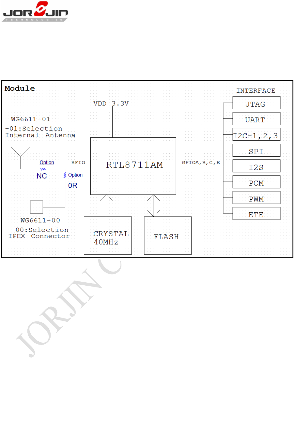
WG6611-00 is a single chip wireless Internet-of-Things module. The advance Realtek
RTL8711AM is a highly integrated single-chip low power 802.11n Wireless LAN (WLAN)
network controller. It combines an ARM-Cortex M3 MCU, WLAN MAC, a 1T1R capable
WLAN baseband, and RF in a single chip. It also provides a bunch of configurable GPIOs
which are configured as digital peripherals for different applications and control usage.
RTL8711AM integrates internal memories for complete WIFI protocol functions. The
embedded memory configuration also provides simple application developments.
FEATURES INTRODUCTION
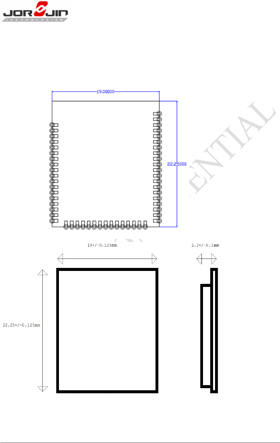
Dimension, L x W x H = 22.25 mm x 19mm x2.3mm (Deviation +/-0.1mm)
Support IEEE 802.11 b/g/n Standard
One Transmit and one Receive path (1T1R)
Frequency range: 2.412GHz – 2.484GHz
ARM® Cortex®-M3 Core
CPU Clock: 166MHz
Memory capacity: 512kB of ROM
1MB of Flash
448kB of SRAM
Operating Voltage: DC 3.3V
Other interface: UART, JTAG, I2S, I2C, SPI, ETE(External Timer Trigger Event),PCM,PWM
RoHS Compliant
Module is for Client mode & Address point & Router
Default is for RF IPEX Connector
Antenna Type(1T1R) Gain(dBi): 3.58
Crystal: 40MHz
Doc No: WG6611-00-DTS-D08
Copyright © JORJIN TECHNOLOGIES INC. 2017
http://WWW.JORJIN.COM.TW
CONFIDENTIAL
Page 4
3. FUNCTIONAL FEATURES
3.1. Module Block Diagram
Doc No: WG6611-00-DTS-D08
Copyright © JORJIN TECHNOLOGIES INC. 2017
http://WWW.JORJIN.COM.TW
CONFIDENTIAL
Page 5
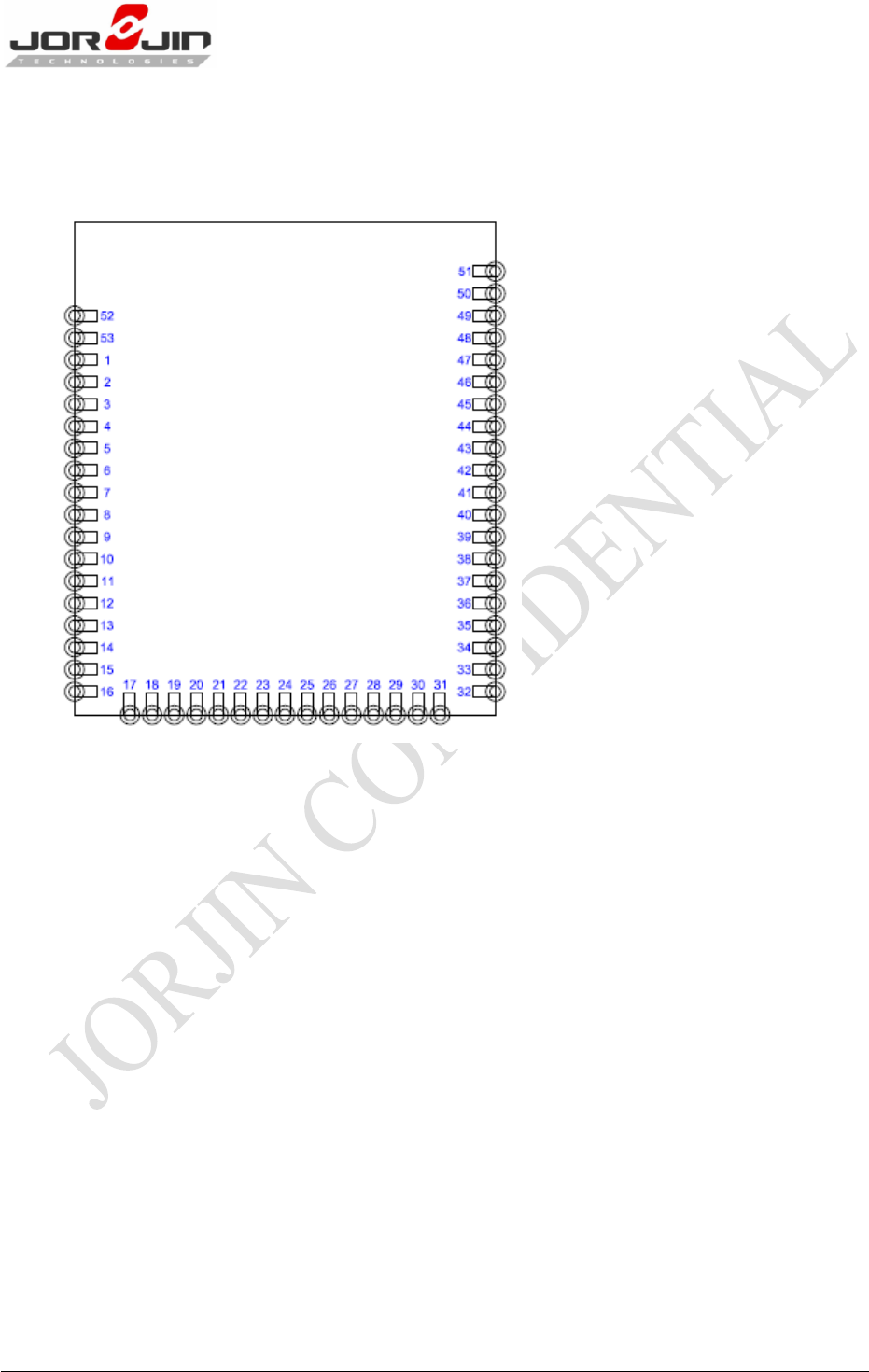
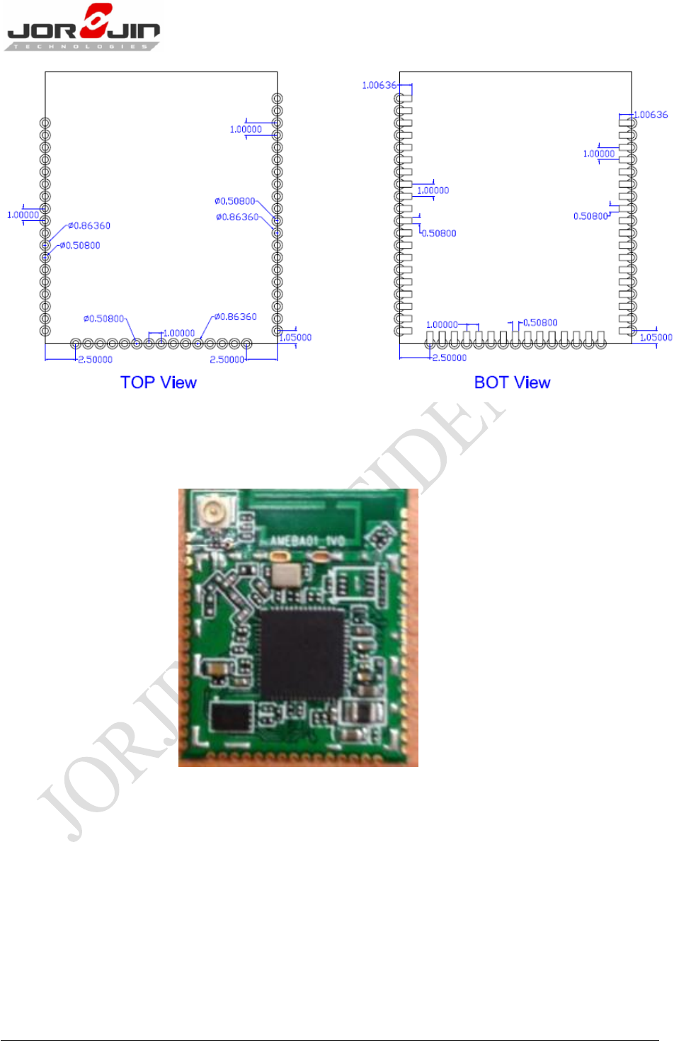
3.2. Pin Assignment (Top view)

Doc No: WG6611-00-DTS-D08
Copyright © JORJIN TECHNOLOGIES INC. 2017
http://WWW.JORJIN.COM.TW
CONFIDENTIAL
Page 6
3.3. Pin Description
Pin#
Name
Description
Type
1
GND
Ground
G
2
GND
Ground
G
3
NC
Not Connected is not used
N
4
NC
Not Connected is not used
N
5
NC
Not Connected is not used
N
6
NC
Not Connected is not used
N
7
VDDIO(1.8~3.3V)
GPIOE, GPIOC, GPIOA, GPIOB
group IO power
P
8
NC
Not Connected is not used
N
9
SWCLK/GPIOE_4
Clock into the core
I/O
10
SWDIO/GPIOE_3
SWD data in/out
I/O
11
GPIOE_2/PWM2
GPIO Pin, PWM(multiplexing)
I/O
12
GPIOE_1/I2C2_SDA/PWM1
GPIO Pin, PWM, I2C(multiplexing)
I/O
13
GPIOE_0/I2C2_SCL
GPIO Pin, I2C(multiplexing)
I/O
14
NC
Not Connected is not used
N
15
ADC_CH2
ADC_CH2,AD converter input
I
16
NC
Not Connected is not used
N
17
GND
Ground
G
18
CHIP_EN
1: Enable Chip
0: Disable chip in shutdown mode
I
19
NC
Not Connected is not used
N
20
NC
Not Connected is not used
N
21
NC
Not Connected is not used
N
22
GPIOA_3/UART0_RTS
GPIO Pin, UART(multiplexing)
I/O
23
NC
Not Connected is not used
N
24
GPIOA_5/UART0_CTS
GPIO Pin, UART(multiplexing)
I/O
25
GPIOA_7/UART0_TXD
GPIO Pin, UART(multiplexing)
I/O
26
GPIOA_6/UART0_RXD
GPIO Pin, UART(multiplexing)
I/O
27
GND
Ground
G
28
NC
Not Connected is not used
N
29
NC
Not Connected is not used
N
30
GND
Ground
G
31
NC
Not Connected is not used
N
32
NC
Not Connected is not used
N
Doc No: WG6611-00-DTS-D08
Copyright © JORJIN TECHNOLOGIES INC. 2017
http://WWW.JORJIN.COM.TW
CONFIDENTIAL
Page 7
33
GND
Ground
G
34
VD33
3.3V Power Supply
P
35
GND
Ground
G
36
GPIOC_3/SPI0_MISO/I2S1_MCK
GPIO Pin, SPI, I2S(multiplexing)
I/O
37
GPIOC_2/SPI0_MOSI/ I2S1_SD_TX
GPIO Pin, SPI, I2S(multiplexing)
I/O
38
GPIOC_1/SPI0_CLK/I2S1_CLK
GPIO Pin, SPI, I2S(multiplexing)
I/O
39
GPIOC_0/PWM0/I2S1_WS
GPIO Pin, PWM, I2S(multiplexing)
I/O
40
GPIOC_4/SPI0_CS1/I2S1_SD_RX
GPIO Pin, SPI, I2S(multiplexing)
I/O
41
GPIOC_5
GPIO Pin
I/O
42
GPIOB_3/I2C3_SDA
GPIO Pin, I2C(multiplexing)
I/O
43
GPIOB_2/I2C3_SCL/NORMAL_MODE_SEL
GPIO Pin, /I2C(multiplexing),
Shared with GPIOB_2
1:Normal operation
0:Enter into test/debug mode
I/O
44
UART_RXD/GPIOB_1
UART_LOG_IN(Debug)
I/O
45
UART_TXD/GPIOB_0/BOOT_SCENARIO
UART_LOG_OUT(Debug),
Shared with GPIOB_0
0:booting from flash
1:booting from internal memory
I/O
46
NC
Not Connected is not used
N
47
NC
Not Connected is not used
N
48
GND
Ground
G
49
NC
Not Connected is not used
N
50
NC
Not Connected is not used
N
51
GND
Ground
G
52
GND
Ground
G
53
NC
Not Connected is not used
N
4. FUNCTIONAL SPECIFICATION
Main Chipset
Realtek RTL8711AM
Wireless standard
IEEE 802.11 b/g /n
Frequency
2.4~2.483GHz ISM Band
Transmit Speed
802.11b: 11,5.5,2,1 Mbps
802.11g: 54,48,36,24,18,12,9,6 Mbps
802.11n: up to 150Mbps

Doc No: WG6611-00-DTS-D08
Copyright © JORJIN TECHNOLOGIES INC. 2017
http://WWW.JORJIN.COM.TW
CONFIDENTIAL
Page 8
Wireless Security
WPAK2-AES(802.11i(WPA,WP2))
OPEN,shared key,and pair-wise key authentication services
Channel
Channel 1~14
Modulation
802.11b(DSSS): CCK(11, 5.5Mbps), DQPSK(2Mbps),
DBPSK(1Mbps);
802.11g(OFDM): BPSK(9,6Mbps), QPSK(18,12Mbps),
16QAM(36,24Mbps), 64QAM(54,48Mbps);
802.11n(OFDM): BPSK, QPSK, 16QAM, 64QAM(150Mbps)
Sensitivity
150Mbps: Typical - 64dBm @ 10% PER
54Mbps: Typical - 65dBm @ 10% PER
11Mbps: Typical - 76dBm @ 8% PER
TX Power
11Mbps: 802.11b 17±2dBm
54Mbps:802.11g 14±2dBm
150Mbps:802.11n 13±2dBm
EVM
11Mbps: 802.11b EVM≦8%
54Mbps:802.11g EVM≦-28dB
150Mbps:802.11n EVM≦-30dB
Antenna
RF path selection feature
-00 : IPEX Connector
-01 : Internal Antenna
Network Architecture
AP Mode (Default)
Client Mode
I/O Voltage Level
Please refer to Table 1 and Table 2 below
UART x2
(Maximum 2 high speed UART interface with baud rate up to
4Mbps)
I2C x3
(Three speeds:
Standard mode(0 to 100 Kb/s)
Fast mode(<400Kb/s)
High-speed mode(<3.4Mb/s)(with appropriate bus loading)
I/O
Interface
I2S x1
(Support 8/16/24/32/48/96KHz,44.1/88.2KHz)
SPI x2
(Support Master/Slave mode(SPI0 only),and Slave only(SPI1 and
SPI2);
Doc No: WG6611-00-DTS-D08
Copyright © JORJIN TECHNOLOGIES INC. 2017
http://WWW.JORJIN.COM.TW
CONFIDENTIAL
Page 9
Support DMA to offload CPU bandwidth.
1 very high speed SPI with baud rate up to 41 MHz.
1 high speed SPI with baud rate up to 10MHz).
PWM x4
(PWM with configurable duration and duty cycle from 0 ~ 100%)
GPIO x19
PCM x2
(Master clock output:64,128,256,or 512kHz)
ETE x1
Dimensions
22.25 x 19 x2.3mm
Table1-Typeical Digital IO DC Parameters(3.3V Case)
Symbol
Parameter
Min
Typ.
Max
Units
VIH
Input-High-Voltage
2.0
V
VIL
Input-Low-Voltage
0.8
V
VOH
Output-High-Voltage
2.4
V
VOL
Output-Low-Voltage
0.4
V
Table2-Typeical Digital IO DC Parameters(1.8V Case)
Symbol
Parameter
Min
Typ.
Max
Units
VIH
Input-High-Voltage
0.65xVcc
V
VIL
Input-Low-Voltage
0.35xVcc
V
VOH
Output-High-Voltage
Vcc-0.45
V
VOL
Output-Low-Voltage
0.45
V
Doc No: WG6611-00-DTS-D08
Copyright © JORJIN TECHNOLOGIES INC. 2017
http://WWW.JORJIN.COM.TW
CONFIDENTIAL
Page 10
4.1. Temperature Limit Ratings
Parameter
Min.
Max.
Units
Storage Temperature
-40
+80
℃
Operating Temperature
0
+70
℃
4.2. DC POWER SUPPLY
Symbol
Parameter
Min
Typ.
Max
Units
VDD
3.3V Supply Voltage
3.0
3.3
3.6
V
VDIO
Digital IO Supply
Voltage
1.62
1.8~3.3
3.6
V
Doc No: WG6611-00-DTS-D08
Copyright © JORJIN TECHNOLOGIES INC. 2017
http://WWW.JORJIN.COM.TW
CONFIDENTIAL
Page 11
4.3. Current Consumption
State
Current(3.3V)
Description
Deep Sleep
5.5uA
Low Power Timer and GPIO Evnet Wakeup
Deep Standby
25uA
Low Power Timer and GPIO Evnet Wakeup
Sleep
0.5mA
Associated with AP but no traffic
Associated Idle (DTIM=1)
3.3mA
Associated with AP and no traffic
Associated Idle (DTIM=2)
2.41mA
Associated with AP and no traffic
Associated Idle (DTIM=3)
1.985mA
Associated with AP and no traffic
Run in Active clock
25mA
CPU clock 166MHz, UART/SPI/I2C available
WiFi is disable
11n RX Mode
62mA
CPU clock 166MHz, UART/SPI/I2C available
WiFi is in 11n Rx
11n TX Throughput
@ 13dBm
162mA
CPU clock 166MHz, UART/SPI/I2C available
WiFi is in 11n Tx transmitting data(throughput)
WiFi is in 11n Rx
Mode
Condition
Typical Current at 3.3V
Active:
TX at 11 Mbps
343mA
TX at 54 Mbps
282mA
TX at HT20-MCS7
267mA
TX at HT40-MCS7
262mA
RX at 11Mbps
68mA
RX at 54Mbps
74mA
RX at HT20-MCS7
74mA
RX at HT40-MCS7
74mA
Doc No: WG6611-00-DTS-D08
Copyright © JORJIN TECHNOLOGIES INC. 2017
http://WWW.JORJIN.COM.TW
CONFIDENTIAL
Page 12
4.4. WLAN 2.4-GHz RF Performance
2.4G WLAN Transmitter
Characteristics
Condition
Min
Typ.
Max
Unit
11b Output Power
11M CCK
17
dBm
1M DSSS
17
11g Output Power
54M OFDM
14
6M OFDM
16
11n Output Power
MCS7
13
MCS0
15
2.4G WLAN Receiver
Characteristics
Condition
Min
Tyd
Max
Unit
11b Rx Sensitivity
11M CCK
-76
dBm
1M DSSS
-83
11g Rx Sensitivity
54M OFDM
-65
6M OFDM
-82
11n Rx Sensitivity
MCS7
-64
MCS0
-82
Note: IPEX Connector Test RF Performance Measurement
Doc No: WG6611-00-DTS-D08
Copyright © JORJIN TECHNOLOGIES INC. 2017
http://WWW.JORJIN.COM.TW
CONFIDENTIAL
Page 13
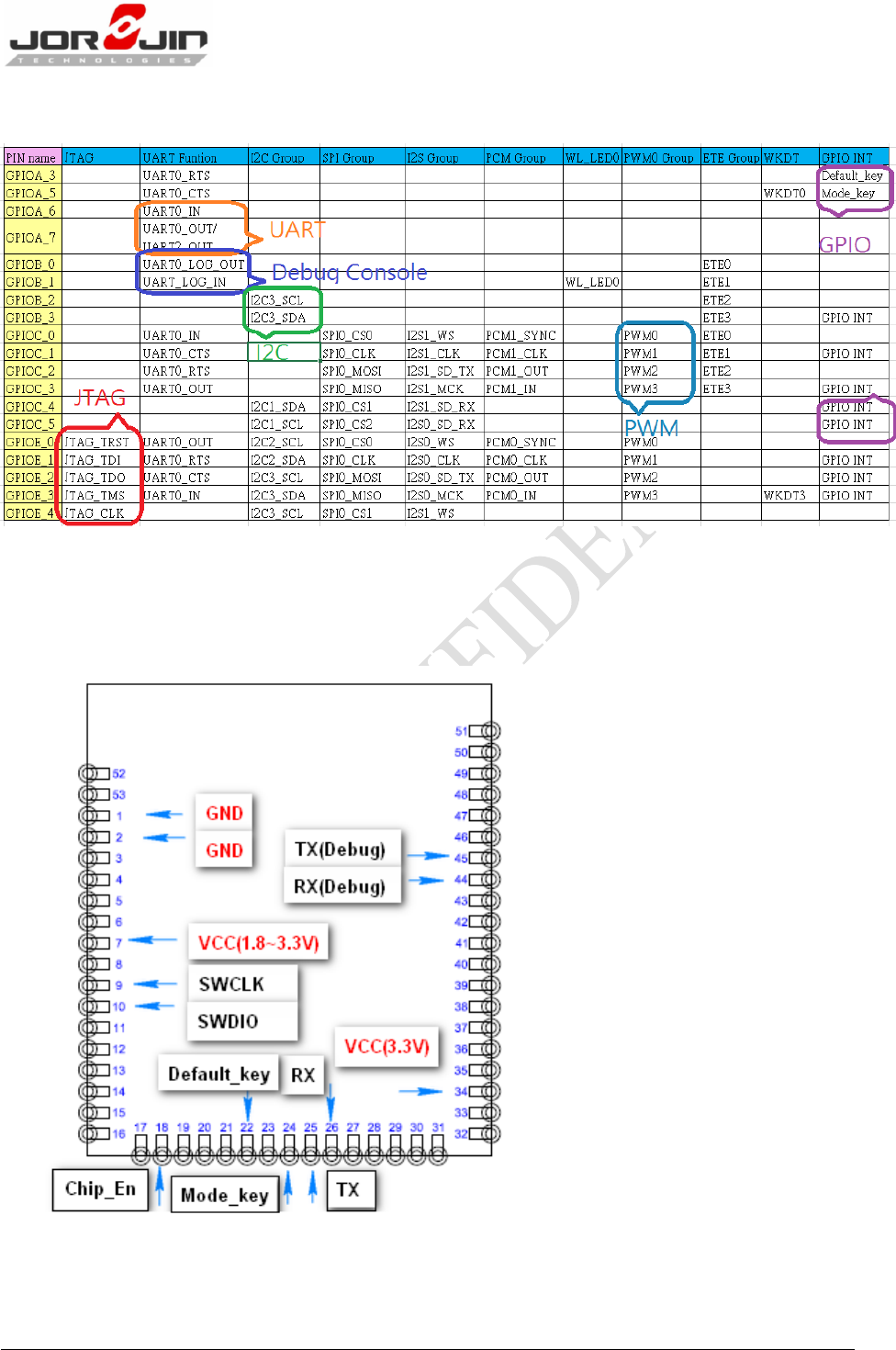
4.5. Pin Function Table
Doc No: WG6611-00-DTS-D08
Copyright © JORJIN TECHNOLOGIES INC. 2017
http://WWW.JORJIN.COM.TW
CONFIDENTIAL
Page 14
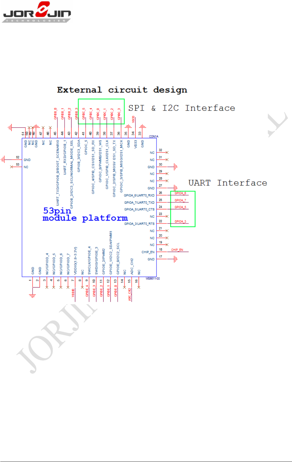
5. REFFERENCE SCHEMATIC
5.1. Application Reference Circuit
Doc No: WG6611-00-DTS-D08
Copyright © JORJIN TECHNOLOGIES INC. 2017
http://WWW.JORJIN.COM.TW
CONFIDENTIAL
Page 15
6. PACKAGE INFORMATION
6.1. Module mechanical outline
Doc No: WG6611-00-DTS-D08
Copyright © JORJIN TECHNOLOGIES INC. 2017
http://WWW.JORJIN.COM.TW
CONFIDENTIAL
Page 16
Module TOP VIEW
Doc No: WG6611-00-DTS-D08
Copyright © JORJIN TECHNOLOGIES INC. 2017
http://WWW.JORJIN.COM.TW
CONFIDENTIAL
Page 17
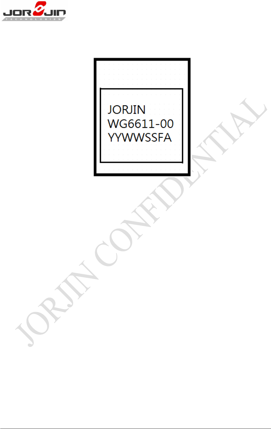
6.2. Package Marking
Data Code: YYWWSSFA
YY = Digit of the year, ex: 2012=12
WW = Week (01~52)
SS = Serial number from 01~98 match to MFG’s lot number or 99 to repair control code
F = Reverse for internal use
A = Module version from A to Z
Doc No: WG6611-00-DTS-D08
Copyright © JORJIN TECHNOLOGIES INC. 2017
http://WWW.JORJIN.COM.TW
CONFIDENTIAL
Page 18
7. SMT AND BAKING RECOMMENDATION
7.1. Baking Recommendation
Baking condition:
- Follow MSL Level 4 to do baking process.
- After bag is opened, devices that will be subjected to reflow solder or other high
temperature process must be
a) Mounted within 72 hours of factory conditions <30°C/60% RH, or
b) Stored at <10% RH.
- Devices require bake, before mounting, if Humidity Indicator Card reads >10%
If baking is required, Devices may be baked for 8 hrs at 125 °C.
7.2. SMT Recommendation
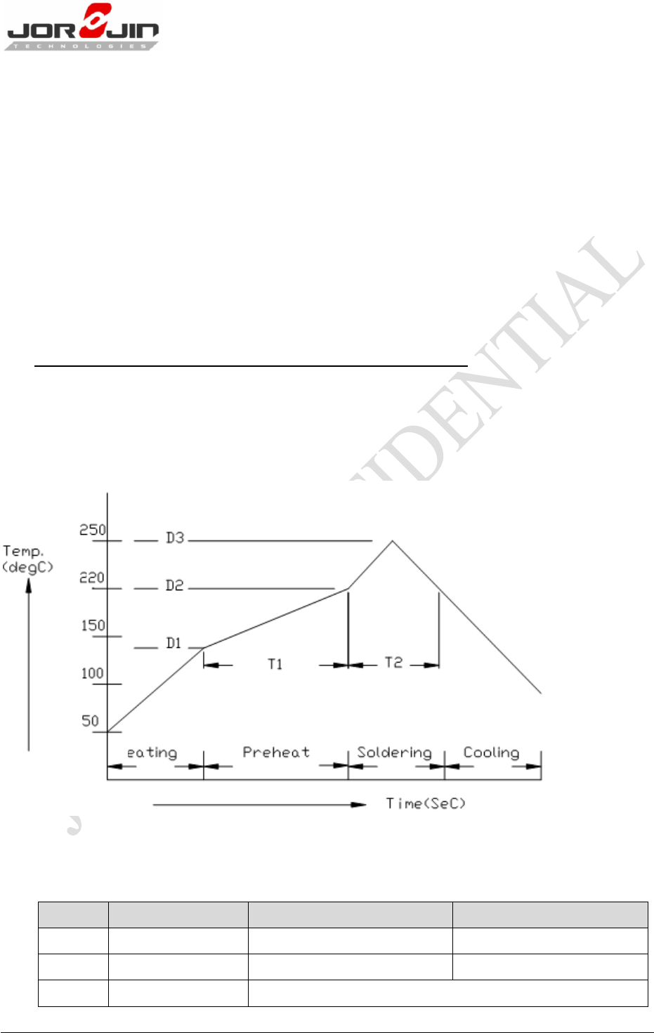
Recommended Reflow profile:
No.
Item
Temperature (°C)
Time (sec)
1
Pre-heat
D1: 140 ~ D2: 200
T1: 80 ~ 120
2
Soldering
D2: = 220
T2: 60 ± 10
3
Peak-Temp.
D3: 250 °C max
H

Doc No: WG6611-00-DTS-D08
Copyright © JORJIN TECHNOLOGIES INC. 2017
http://WWW.JORJIN.COM.TW
CONFIDENTIAL
Page 19
Note: (1) Reflow soldering is recommended two times maximum.
(1) Add Nitrogen while Reflow process: SMT solder ability will be better.
Stencil thickness: 0.1~ 0.15 mm (Recommended)
Soldering paste (without Pb): Recommended SENJU N705-GRN3360-K2-V can get better
soldering effects.

Doc No: WG6611-00-DTS-D08
Copyright © JORJIN TECHNOLOGIES INC. 2017
http://WWW.JORJIN.COM.TW
CONFIDENTIAL
Page 20
FCC Statement
This equipment has been tested and found to comply with the limits for a Class B digital device,
pursuant to part 15 of the FCC Rules. These limits are designed to provide reasonable protection
against harmful interference in a residential installation. This equipment generates, uses and can
radiate radio frequency energy and, if not installed and used in accordance with the instructions,
may cause harmful interference to radio communications. However, there is no guarantee that
interference will not occur in a particular installation. If this equipment does cause harmful
interference to radio or television reception, which can be determined by turning the equipment off
and on, the user is encouraged to try to correct the interference by one or more of the following
measures:
—Reorient or relocate the receiving antenna.
—Increase the separation between the equipment and receiver.
—Connect the equipment into an outlet on a circuit different from that to which the receiver is
connected.
—Consult the dealer or an experienced radio/TV technician for help.
FCC Radiation Exposure Statement
This device complies with FCC radiation exposure limits set forth for an uncontrolled environment
and it also complies with Part 15 of the FCC RF Rules. This equipment must be installed and
operated in accordance with provided instructions and the antenna(s) used for this transmitter
must be installed to provide a separation distance of at least 20 cm from all persons and must not
be co-located or operating in conjunction with any other antenna or transmitter. End-users and
installers must be provided with antenna installation instructions and consider removing the
no-collocation statement.
This device complies with Part 15 of the FCC Rules. Operation is subject to the following two
conditions:
(1) this device may not cause harmful interference, and
(2) this device must accept any interference received, including interference that may cause
undesired operation.
Caution!
Any changes or modifications not expressly approved by the party responsible for compliance could
void the user's authority to operate the equipment.

Doc No: WG6611-00-DTS-D08
Copyright © JORJIN TECHNOLOGIES INC. 2017
http://WWW.JORJIN.COM.TW
CONFIDENTIAL
Page 21
This device is intended only for OEM integrators under the following conditions:
1) The antenna must be installed such that 20cm is maintained between the antenna and users,
and
2) The transmitter module may not be co-located with any other transmitter or antenna,
3) For all products market in US, OEM has to limit the operation channels in CH1 to CH11 for
2.4Gband by supplied firmware programming tool. OEM shall not supply any tool or info to the
end-user regarding to Regulatory Domain change.
As long as 3 conditions above are met, further transmitter test will not be required. However, the
OEM integrator is still responsible for testing their end-product for any additional compliance
requirements required with this module installed.
IMPORTANT NOTE:
In the event that these conditions can not be met (for example certain laptop configurations or
co-location with another transmitter), then the FCC authorization is no longer considered valid and
the FCC ID can not be used on the final product. In these circumstances, the OEM integrator will be
responsible for re-evaluating the end product (including the transmitter) and obtaining a separate
FCC authorization.
End Product Labelling
The final end product must be labelled in a visible area with the following:
“Contains FCC ID:WS2-WG6611.
Manual Information to the End User
The OEM integrator has to be aware not to provide information to the end user regarding how
to install or remove this RF module in the user’s manual of the end product which integrates this
module.