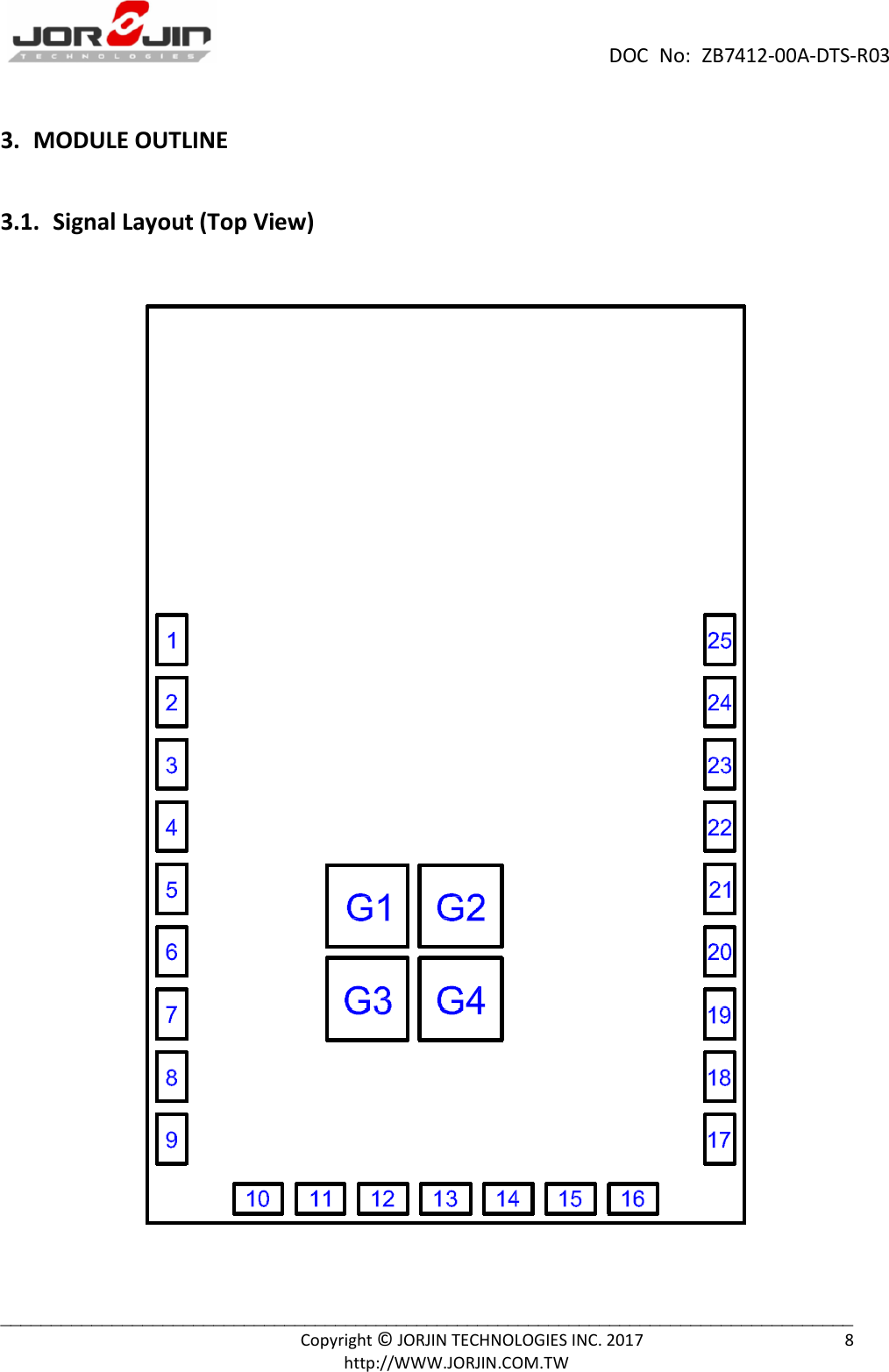
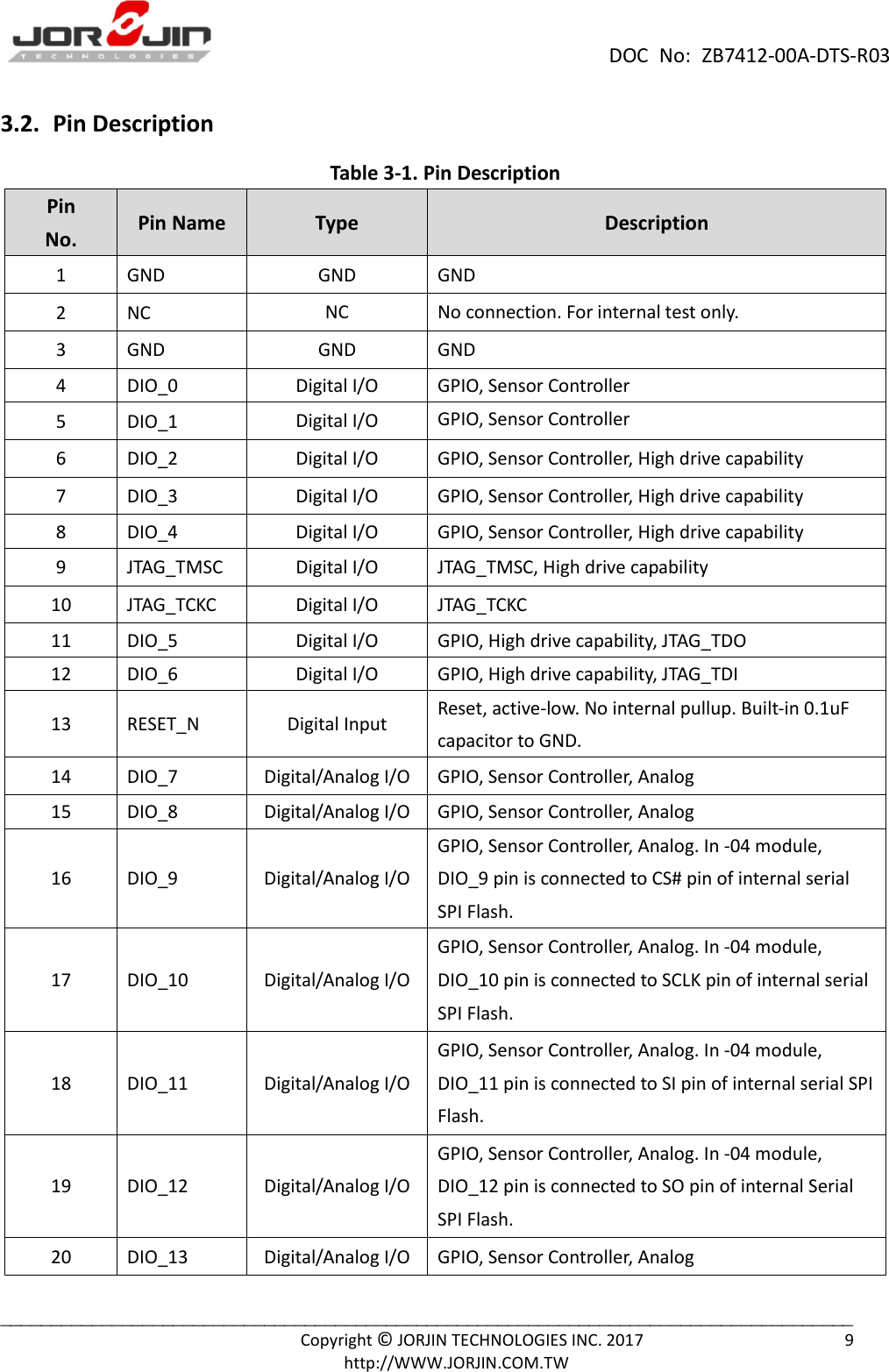
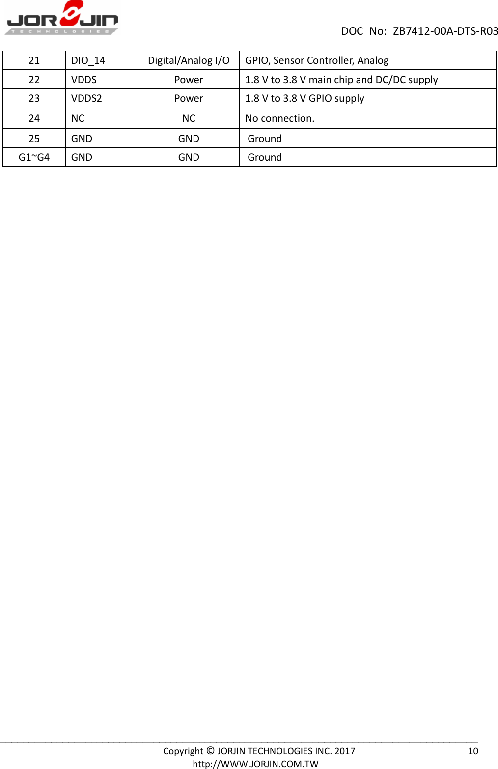
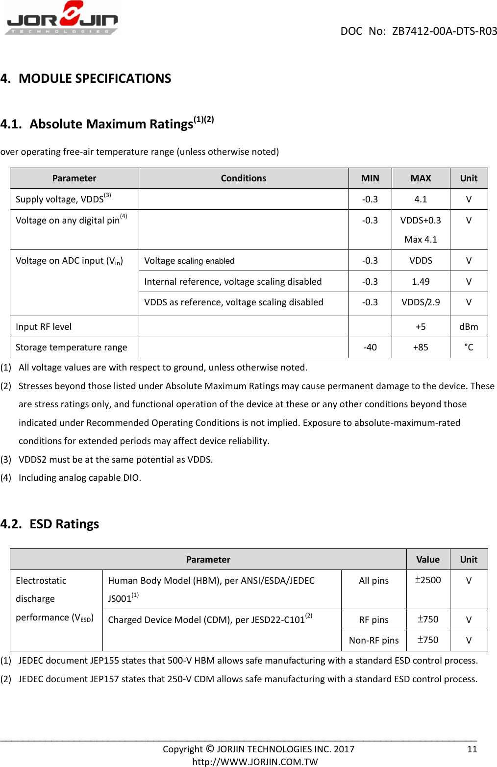
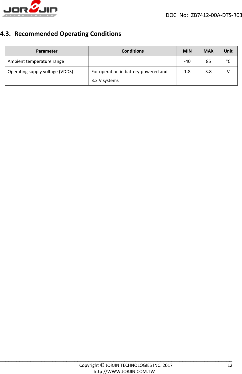
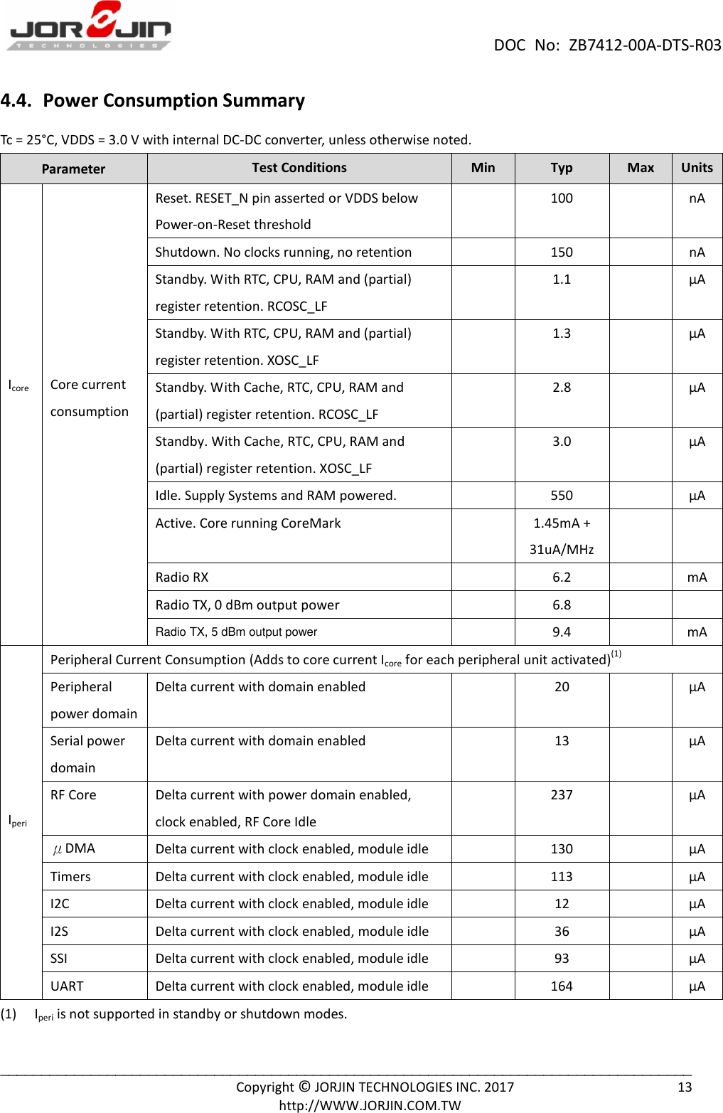
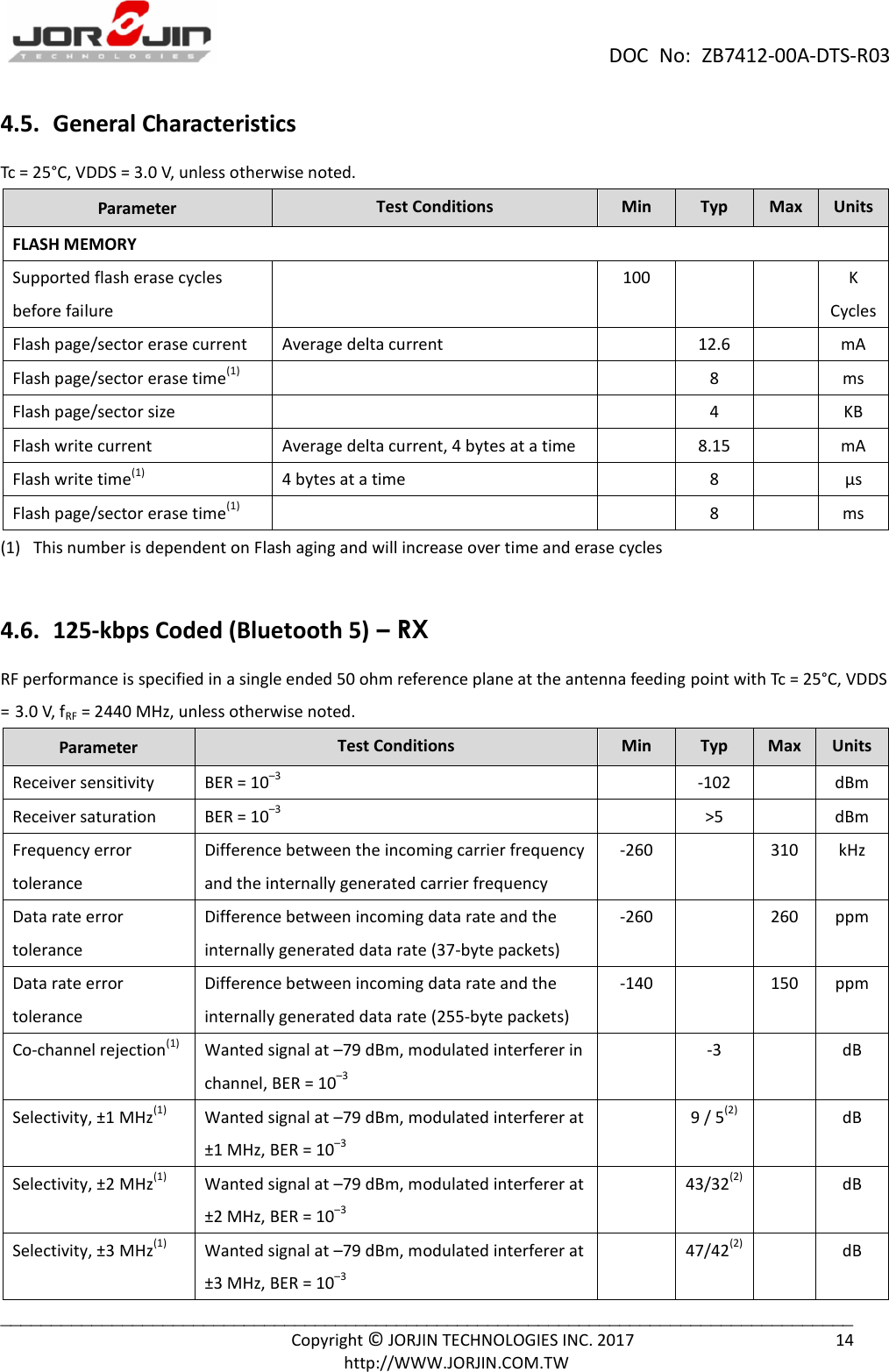
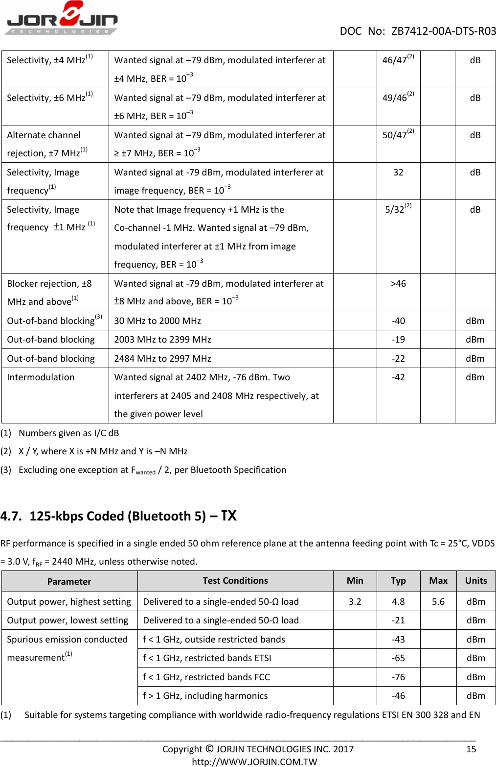
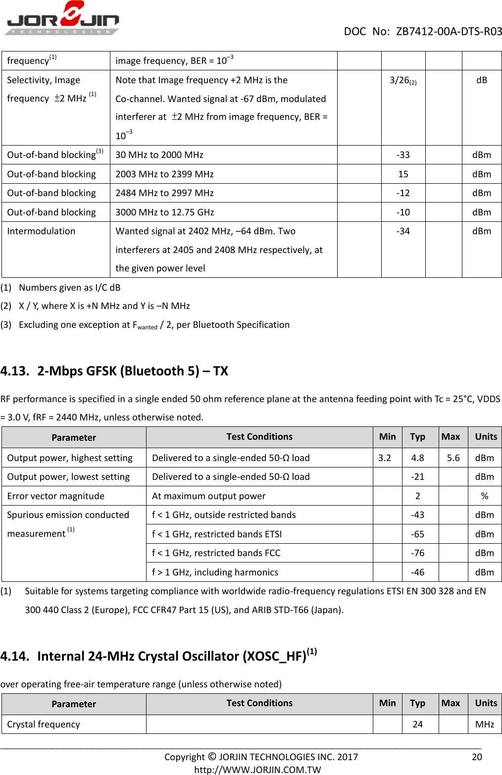
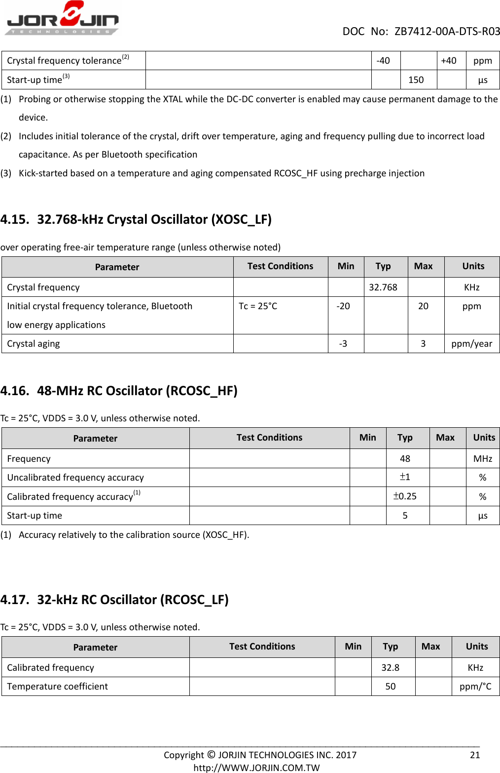
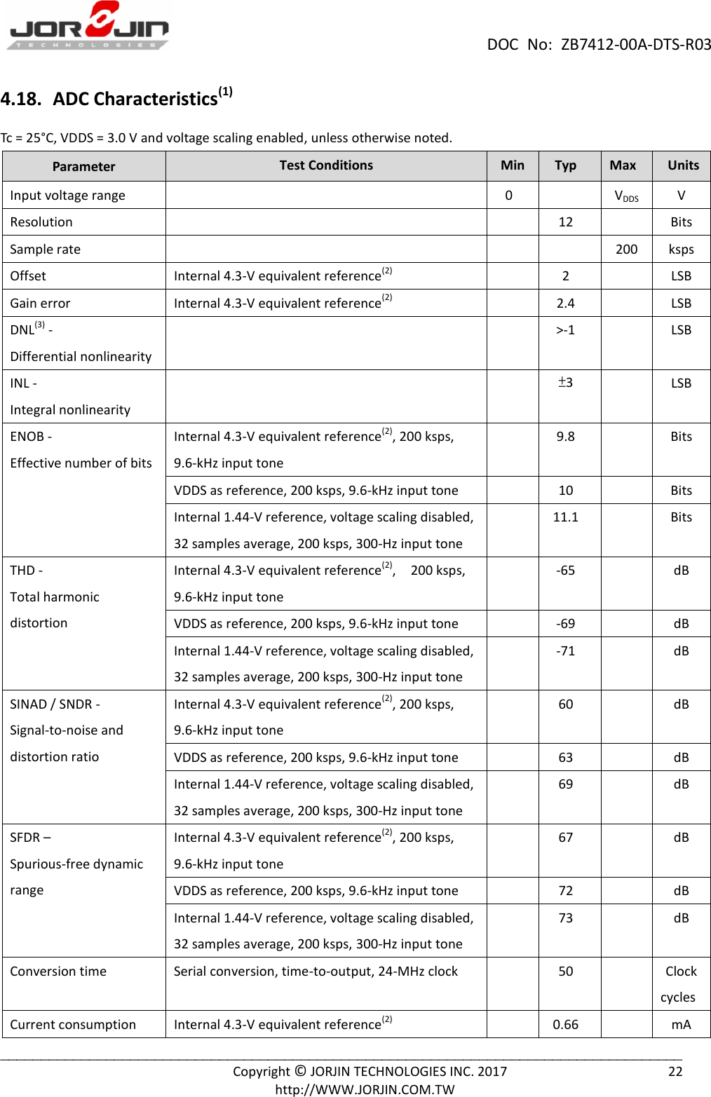
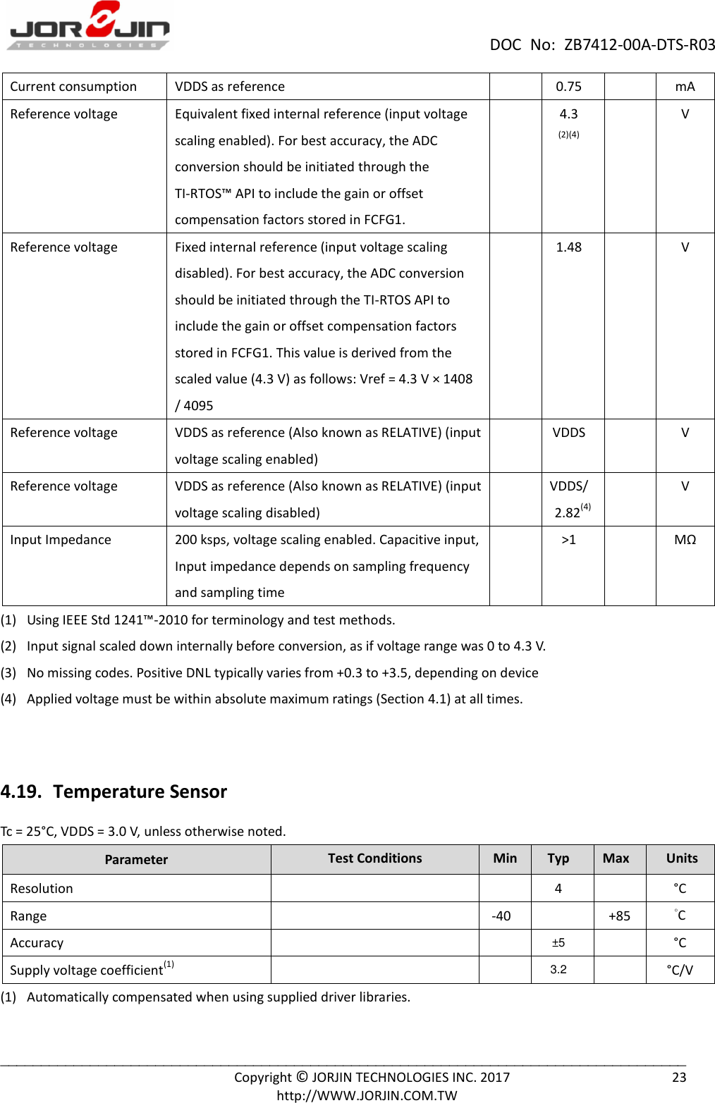
Jorjin Technologies ZB7412 BLE wireless module User Manual 1

Jorjin Technologies Inc. BLE wireless module 1

User Manual

-------------------------------------------------------------------------------------------------------------------------------------------------- Copyright ©  JORJIN TECHNOLOGIES INC. 2017 http://WWW.JORJIN.COM.TW  a module solution provider   ZB7412-00   SimpleLinkTM    Bluetooth®  Low Energy   Wireless MCU Module  TI  CC2640R2F  Solution      Datasheet Revision 0.3  Prepared By Reviewed By Approved By
                                           DOC  No:  ZB7412-00A-DTS-R03  ____________________________________________________________________________________         Copyright © JORJIN TECHNOLOGIES INC. 2017                                            1             http://WWW.JORJIN.COM.TW Index 1. OVERVIEW ....................................................................................................................................... 3 1.1. GENERAL FEATURES ........................................................................................................................ 3 1.2. APPLICATIONS ................................................................................................................................ 4 2. FUNCTIONAL FEATURES .................................................................................................................. 5 2.1. MODULE BLOCK DIAGRAM ............................................................................................................... 5 2.2. BLOCK FUNCTIONAL FEATURE ........................................................................................................... 6 Microcontroller ............................................................................................................................ 6 Ultra-Low Power Sensor Controller ............................................................................................ 6 Peripherals ................................................................................................................................... 6 RF Section .................................................................................................................................... 7 3. MODULE OUTLINE ........................................................................................................................... 8 3.1. SIGNAL LAYOUT (TOP VIEW) ............................................................................................................. 8 3.2. PIN DESCRIPTION ........................................................................................................................... 9 4. MODULE SPECIFICATIONS ............................................................................................................. 11 4.1. ABSOLUTE MAXIMUM RATINGS(1)(2) ................................................................................................. 11 4.2. ESD RATINGS .............................................................................................................................. 11 4.3. RECOMMENDED OPERATING CONDITIONS ......................................................................................... 12 4.4. POWER CONSUMPTION SUMMARY .................................................................................................. 13 4.5. GENERAL CHARACTERISTICS ............................................................................................................ 14 4.6. 125-KBPS CODED (BLUETOOTH 5) – RX .......................................................................................... 14 4.7. 125-KBPS CODED (BLUETOOTH 5) – TX .......................................................................................... 15 4.8. 500-KBPS CODED (BLUETOOTH 5) – RX .......................................................................................... 16 4.9. 500-KBPS CODED (BLUETOOTH 5) – TX .......................................................................................... 17 4.10. 1-MBPS GFSK (BLUETOOTH LOW ENERGY) – RX ............................................................................. 17 4.11. 1-MBPS GFSK (BLUETOOTH LOW ENERGY) – TX ............................................................................. 19 4.12. 2-MBPS GFSK (BLUETOOTH 5) – RX ............................................................................................. 19 4.13. 2-MBPS GFSK (BLUETOOTH 5) – TX ............................................................................................. 20 4.14. INTERNAL 24-MHZ CRYSTAL OSCILLATOR (XOSC_HF)(1) .................................................................. 20 4.15. 32.768-KHZ CRYSTAL OSCILLATOR (XOSC_LF) ............................................................................... 21 4.16. 48-MHZ RC OSCILLATOR (RCOSC_HF) ........................................................................................ 21 4.17. 32-KHZ RC OSCILLATOR (RCOSC_LF) .......................................................................................... 21 4.18. ADC CHARACTERISTICS(1) ............................................................................................................ 22 4.19. TEMPERATURE SENSOR ................................................................................................................ 23
                                           DOC  No:  ZB7412-00A-DTS-R03  ____________________________________________________________________________________         Copyright © JORJIN TECHNOLOGIES INC. 2017                                            2             http://WWW.JORJIN.COM.TW 4.20. BATTERY MONITOR ..................................................................................................................... 24 4.21. CONTINUOUS TIME COMPARATOR ................................................................................................. 24 4.22. LOW-POWER CLOCKED COMPARATOR............................................................................................. 24 4.23. PROGRAMMABLE CURRENT SOURCE .............................................................................................. 25 4.24. DC CHARACTERISTICS .................................................................................................................. 25 4.25. TIMING REQUIREMENTS ............................................................................................................... 26 4.26. SWITCHING CHARACTERISTICS ....................................................................................................... 27 4.27. TYPICAL CHARACTERISTICS ............................................................................................................ 29 4.28. CHIP ANTENNA CHARACTERISTICS .................................................................................................. 30 5. DESIGN RECOMMENDATIONS ....................................................................................................... 32 5.1. MODULE LAYOUT RECOMMENDATIONS ............................................................................................ 32 5.2. REFERENCE SCHEMATIC ................................................................................................................. 34 6. PACKAGE INFORMATION ............................................................................................................... 35 6.1. MODULE MECHANICAL OUTLINE ..................................................................................................... 35 6.2. ORDERING INFORMATION............................................................................................................... 36 6.3. PACKAGE MARKING ...................................................................................................................... 37 7. SMT AND BAKING RECOMMENDATION ....................................................................................... 39 7.1. BAKING RECOMMENDATION ........................................................................................................... 39 7.2. SMT RECOMMENDATION .............................................................................................................. 39 8. TAPE REEL INFROMATION ............................................................................................................. 41 8.1. COVER / CARRIER TAPE DIMENSION ................................................................................................. 41 9. REGULATORY INFORMATION ........................................................................................................ 42 9.1. UNITED STATES ............................................................................................................................ 42 9.2. CANADA ..................................................................................................................................... 43 9.3. EUROPE ...................................................................................................................................... 44 9.4. JAPAN ........................................................................................................................................ 44 9.5. TAIWAN ...................................................................................................................................... 45 9.6. AUSTRALIA/NEW ZEALAND ............................................................................................................ 46 10. HISTORY CHANGE ........................................................................................................................ 47
                                           DOC  No:  ZB7412-00A-DTS-R03  ____________________________________________________________________________________         Copyright © JORJIN TECHNOLOGIES INC. 2017                                            3             http://WWW.JORJIN.COM.TW 1.  OVERVIEW The certified ZB7412-00 module from JORJIN is a wireless MCU module targeting Bluetooth 4.2 and Bluetooth 5 low energy applications. This module is based on TI CC2640R2F wireless MCU QFN-32 package chip.  The module is a cost-effective, ultralow power, 2.4-GHz RF devices. Very low active RF and MCU current and low-power mode current consumption provide excellent battery lifetime and allow for operation on small coin cell batteries and in energy-harvesting applications.  1.1.  General Features  TI CC2640R2F, 24MHz & 32.768KHz crystals, DC2DC, and chip antenna on a single module.  Built-in TI CC2640R2F 5x5mm RHB VQFN32 (15 GPIOs)  LGA 25pins package.  Dimension 16.9mm(L) x 11mm(W) x 2.45mm(H)  Powerful ARM® Cortex®-M3 Microcontroller  Ultra-Low Power Sensor Controller  Efficient Code Size Architecture, Placing Drivers, TI-RTOS, and Bluetooth® Software in ROM to Make More Flash Available for the Application  No external component required.  Low Power and Wide Supply Voltage Range: 1.8 to 3.8V -  Internal DC-DC converter built-in  2.4-GHz RF Transceiver and Integrated Antenna.  Suitable for Systems Targeting Compliance With Worldwide Radio Frequency Regulations -  ETSI EN 300 328 (Europe) -  EN 300 440 Class 2 (Europe) -  FCC CFR47 Part 15 (US) -  ARIB STD-T66 (Japan)  Tools and Development Environment from TI -  Full-Feature and Low-Cost Development Kits -  Packet Sniffer PC Software -  Sensor Controller Studio -  SmartRF™ Studio -  SmartRF Flash Programmer 2 -  IAR Embedded Workbench® for ARM
                                           DOC  No:  ZB7412-00A-DTS-R03  ____________________________________________________________________________________         Copyright © JORJIN TECHNOLOGIES INC. 2017                                            4             http://WWW.JORJIN.COM.TW -  Code Composer Studio™  1.2.  Applications  Home and Building Automation -  Connected Appliances -  Lighting -  Locks -  Gateways -  Security Systems  Industrial -  Logistics -  Production and Manufacturing Automation -  Asset Tracking and Management -  HMI and Remote Display -  Access Control  Retail -  Beacons -  Advertising -  ESL and Price Tags -  Point of Sales and Payment Systems  Health and Medical -  Thermometers -  Blood Glucose and Pressure Meters -  Weight Scales -  Hearing Aids  Sports and Fitness -  Activity Monitors and Fitness Trackers -  Heart Rate Monitors -  Running and Biking Sensors -  Sports Watches -  Gym Equipment -  Team Sports Equipment  HID -  Voice Remote Controls -  Gaming -  Keyboards and Mice
                                           DOC  No:  ZB7412-00A-DTS-R03  ____________________________________________________________________________________         Copyright © JORJIN TECHNOLOGIES INC. 2017                                            5             http://WWW.JORJIN.COM.TW 2.  FUNCTIONAL FEATURES 2.1.  Module Block Diagram                                     VDD GPIOs ZB7412-00 module GPIOs
                                           DOC  No:  ZB7412-00A-DTS-R03  ____________________________________________________________________________________         Copyright © JORJIN TECHNOLOGIES INC. 2017                                            6             http://WWW.JORJIN.COM.TW 2.2.  Block Functional Feature  Microcontroller  Powerful ARM® Cortex®-M3  EEMBC CoreMark® score: 142  Up to 48-MHz Clock Speed  275KB of Nonvolatile Memory Including 128KB of In-System Programmable Flash  Up to 28KB of System SRAM, of Which 20KB is Ultra-Low Leakage SRAM  8-KB SRAM for Cache or System RAM Use  2-Pin cJTAG and JTAG Debugging  Supports Over-The-Air Upgrade (OTA)  Ultra-Low Power Sensor Controller  Can run autonomous from the rest of the system  16-Bit Architecture  2-KB Ultra-Low Leakage SRAM for Code and Data  Peripherals  All Digital Peripheral Pins can be routed to any GPIO.  15 GPIOs    4 General-Purpose Timer Modules (Eight 16-Bit or Four 32-Bit Timer, PWM Each)  12-Bit ADC, 200-ksamples/s, 8-Channel Analog MUX  Continuous Time Comparator  Ultra-Low Power Analog Comparator  Programmable Current Source  UART  2x SSI (SPI, MICROWIRE, TI)  I2C  I2S  Real-Time Clock (RTC)
                                           DOC  No:  ZB7412-00A-DTS-R03  ____________________________________________________________________________________         Copyright © JORJIN TECHNOLOGIES INC. 2017                                            7             http://WWW.JORJIN.COM.TW  AES-128 Security Module  True Random Number Generator (TRNG)  Support for 8 Capacitive Sensing Buttons  Integrated Temperature Sensor  RF Section  2.4 GHz RF Transceiver Compatible With Bluetooth Low Energy (BLE) 4.2 and 5 specifications  Excellent Receiver Sensitivity (–96 dBm for BLE), Selectivity, and Blocking Performance  Link budget of 101 dB for BLE.  Programmable Output Power up to +5 dBm  Integrated Antenna  Pre-certified for Compliance With Worldwide Radio Frequency Regulations -  ETSI (Europe) -  IC (Canada) -  FCC (USA) -  ARIB STD-T66 (Japan) -  NCC (Taiwan) -  RCM (Australia and New Zealand)
                                           DOC  No:  ZB7412-00A-DTS-R03  ____________________________________________________________________________________         Copyright © JORJIN TECHNOLOGIES INC. 2017                                            8             http://WWW.JORJIN.COM.TW 3.  MODULE OUTLINE 3.1.  Signal Layout (Top View)
                                           DOC  No:  ZB7412-00A-DTS-R03  ____________________________________________________________________________________         Copyright © JORJIN TECHNOLOGIES INC. 2017                                            9             http://WWW.JORJIN.COM.TW 3.2.  Pin Description Table 3-1. Pin Description Pin No. Pin Name Type Description 1 GND GND GND 2 NC NC No connection. For internal test only. 3 GND GND GND 4 DIO_0 Digital I/O GPIO, Sensor Controller 5 DIO_1 Digital I/O GPIO, Sensor Controller 6 DIO_2 Digital I/O GPIO, Sensor Controller, High drive capability 7 DIO_3 Digital I/O GPIO, Sensor Controller, High drive capability 8 DIO_4 Digital I/O GPIO, Sensor Controller, High drive capability 9 JTAG_TMSC Digital I/O JTAG_TMSC, High drive capability 10 JTAG_TCKC Digital I/O JTAG_TCKC 11 DIO_5 Digital I/O GPIO, High drive capability, JTAG_TDO 12 DIO_6 Digital I/O GPIO, High drive capability, JTAG_TDI 13 RESET_N Digital Input Reset, active-low. No internal pullup. Built-in 0.1uF capacitor to GND. 14 DIO_7 Digital/Analog I/O GPIO, Sensor Controller, Analog 15 DIO_8 Digital/Analog I/O GPIO, Sensor Controller, Analog 16 DIO_9 Digital/Analog I/O GPIO, Sensor Controller, Analog. In -04 module, DIO_9 pin is connected to CS# pin of internal serial SPI Flash. 17 DIO_10 Digital/Analog I/O GPIO, Sensor Controller, Analog. In -04 module, DIO_10 pin is connected to SCLK pin of internal serial SPI Flash. 18 DIO_11 Digital/Analog I/O GPIO, Sensor Controller, Analog. In -04 module, DIO_11 pin is connected to SI pin of internal serial SPI Flash. 19 DIO_12 Digital/Analog I/O GPIO, Sensor Controller, Analog. In -04 module, DIO_12 pin is connected to SO pin of internal Serial SPI Flash. 20 DIO_13 Digital/Analog I/O GPIO, Sensor Controller, Analog
                                           DOC  No:  ZB7412-00A-DTS-R03  ____________________________________________________________________________________         Copyright © JORJIN TECHNOLOGIES INC. 2017                                            10             http://WWW.JORJIN.COM.TW 21 DIO_14 Digital/Analog I/O GPIO, Sensor Controller, Analog 22 VDDS Power 1.8 V to 3.8 V main chip and DC/DC supply 23 VDDS2 Power 1.8 V to 3.8 V GPIO supply 24 NC NC No connection. 25 GND GND  Ground G1~G4 GND GND  Ground
                                           DOC  No:  ZB7412-00A-DTS-R03  ____________________________________________________________________________________         Copyright © JORJIN TECHNOLOGIES INC. 2017                                            11             http://WWW.JORJIN.COM.TW 4.  MODULE SPECIFICATIONS 4.1.  Absolute Maximum Ratings(1)(2) over operating free-air temperature range (unless otherwise noted) (1) All voltage values are with respect to ground, unless otherwise noted. (2) Stresses beyond those listed under Absolute Maximum Ratings may cause permanent damage to the device. These are stress ratings only, and functional operation of the device at these or any other conditions beyond those indicated under Recommended Operating Conditions is not implied. Exposure to absolute-maximum-rated conditions for extended periods may affect device reliability. (3) VDDS2 must be at the same potential as VDDS. (4) Including analog capable DIO.  4.2.  ESD Ratings (1) JEDEC document JEP155 states that 500-V HBM allows safe manufacturing with a standard ESD control process. (2) JEDEC document JEP157 states that 250-V CDM allows safe manufacturing with a standard ESD control process.  Parameter Conditions MIN MAX Unit Supply voltage, VDDS(3)  -0.3 4.1 V Voltage on any digital pin(4)  -0.3 VDDS+0.3 Max 4.1 V Voltage on ADC input (Vin) Voltage scaling enabled -0.3 VDDS V Internal reference, voltage scaling disabled -0.3 1.49 V VDDS as reference, voltage scaling disabled -0.3 VDDS/2.9 V Input RF level   +5 dBm Storage temperature range    -40 +85 °C  Parameter Value Unit Electrostatic discharge performance (VESD) Human Body Model (HBM), per ANSI/ESDA/JEDEC JS001(1) All pins ±2500 V Charged Device Model (CDM), per JESD22-C101(2) RF pins ±750 V Non-RF pins ±750 V
                                           DOC  No:  ZB7412-00A-DTS-R03  ____________________________________________________________________________________         Copyright © JORJIN TECHNOLOGIES INC. 2017                                            12             http://WWW.JORJIN.COM.TW 4.3.  Recommended Operating Conditions  Parameter Conditions MIN MAX Unit Ambient temperature range  -40 85 °C  Operating supply voltage (VDDS) For operation in battery-powered and 3.3 V systems 1.8 3.8 V
                                           DOC  No:  ZB7412-00A-DTS-R03  ____________________________________________________________________________________         Copyright © JORJIN TECHNOLOGIES INC. 2017                                            13             http://WWW.JORJIN.COM.TW 4.4.  Power Consumption Summary Tc = 25°C, VDDS = 3.0 V with internal DC-DC converter, unless otherwise noted. Parameter Test Conditions Min Typ Max Units        Icore          Core current consumption Reset. RESET_N pin asserted or VDDS below Power-on-Reset threshold  100  nA Shutdown. No clocks running, no retention  150  nA Standby. With RTC, CPU, RAM and (partial) register retention. RCOSC_LF  1.1  μA Standby. With RTC, CPU, RAM and (partial) register retention. XOSC_LF  1.3  μA Standby. With Cache, RTC, CPU, RAM and (partial) register retention. RCOSC_LF  2.8  μA Standby. With Cache, RTC, CPU, RAM and (partial) register retention. XOSC_LF  3.0  μA Idle. Supply Systems and RAM powered.  550  μA Active. Core running CoreMark  1.45mA + 31uA/MHz   Radio RX  6.2  mA Radio TX, 0 dBm output power  6.8   Radio TX, 5 dBm output power  9.4  mA       Iperi Peripheral Current Consumption (Adds to core current Icore for each peripheral unit activated)(1) Peripheral power domain Delta current with domain enabled  20  μA Serial power domain Delta current with domain enabled  13  μA RF Core Delta current with power domain enabled, clock enabled, RF Core Idle  237  μA μDMA Delta current with clock enabled, module idle  130  μA Timers Delta current with clock enabled, module idle  113  μA I2C Delta current with clock enabled, module idle  12  μA I2S Delta current with clock enabled, module idle  36  μA SSI Delta current with clock enabled, module idle  93  μA UART Delta current with clock enabled, module idle  164  μA (1)   Iperi is not supported in standby or shutdown modes.
                                           DOC  No:  ZB7412-00A-DTS-R03  ____________________________________________________________________________________         Copyright © JORJIN TECHNOLOGIES INC. 2017                                            14             http://WWW.JORJIN.COM.TW 4.5.  General Characteristics Tc = 25°C, VDDS = 3.0 V, unless otherwise noted. Parameter Test Conditions Min Typ Max Units FLASH MEMORY Supported flash erase cycles before failure  100   K Cycles Flash page/sector erase current Average delta current  12.6  mA Flash page/sector erase time(1)   8  ms Flash page/sector size   4  KB Flash write current Average delta current, 4 bytes at a time  8.15  mA Flash write time(1) 4 bytes at a time  8  μs Flash page/sector erase time(1)   8  ms (1) This number is dependent on Flash aging and will increase over time and erase cycles  4.6.  125-kbps Coded (Bluetooth 5) – RX RF performance is specified in a single ended 50 ohm reference plane at the antenna feeding point with Tc = 25°C, VDDS = 3.0 V, fRF = 2440 MHz, unless otherwise noted. Parameter Test Conditions Min Typ Max Units Receiver sensitivity BER = 10–3  -102  dBm Receiver saturation BER = 10–3  >5  dBm Frequency error tolerance Difference between the incoming carrier frequency and the internally generated carrier frequency -260  310 kHz Data rate error tolerance Difference between incoming data rate and the internally generated data rate (37-byte packets) -260  260 ppm Data rate error tolerance Difference between incoming data rate and the internally generated data rate (255-byte packets) -140  150 ppm Co-channel rejection(1) Wanted signal at –79 dBm, modulated interferer in channel, BER = 10–3  -3  dB Selectivity, ±1 MHz(1) Wanted signal at –79 dBm, modulated interferer at ±1 MHz, BER = 10–3  9 / 5(2)  dB Selectivity, ±2 MHz(1) Wanted signal at –79 dBm, modulated interferer at ±2 MHz, BER = 10–3  43/32(2)  dB Selectivity, ±3 MHz(1) Wanted signal at –79 dBm, modulated interferer at ±3 MHz, BER = 10–3  47/42(2)  dB
                                           DOC  No:  ZB7412-00A-DTS-R03  ____________________________________________________________________________________         Copyright © JORJIN TECHNOLOGIES INC. 2017                                            15             http://WWW.JORJIN.COM.TW Selectivity, ±4 MHz(1) Wanted signal at –79 dBm, modulated interferer at ±4 MHz, BER = 10–3  46/47(2)  dB Selectivity, ±6 MHz(1) Wanted signal at –79 dBm, modulated interferer at ±6 MHz, BER = 10–3  49/46(2)  dB Alternate channel rejection, ±7 MHz(1) Wanted signal at –79 dBm, modulated interferer at ≥ ±7 MHz, BER = 10–3  50/47(2)  dB Selectivity, Image frequency(1) Wanted signal at -79 dBm, modulated interferer at image frequency, BER = 10–3  32  dB Selectivity, Image frequency  ±1 MHz (1) Note that Image frequency +1 MHz is the Co-channel -1 MHz. Wanted signal at –79 dBm, modulated interferer at ±1 MHz from image frequency, BER = 10–3  5/32(2)  dB Blocker rejection, ±8 MHz and above(1) Wanted signal at -79 dBm, modulated interferer at ±8 MHz and above, BER = 10–3  >46   Out-of-band blocking(3) 30 MHz to 2000 MHz  -40  dBm Out-of-band blocking 2003 MHz to 2399 MHz  -19  dBm Out-of-band blocking 2484 MHz to 2997 MHz  -22  dBm Intermodulation Wanted signal at 2402 MHz, -76 dBm. Two interferers at 2405 and 2408 MHz respectively, at the given power level  -42  dBm (1) Numbers given as I/C dB (2) X / Y, where X is +N MHz and Y is –N MHz (3) Excluding one exception at Fwanted / 2, per Bluetooth Specification  4.7.  125-kbps Coded (Bluetooth 5) – TX RF performance is specified in a single ended 50 ohm reference plane at the antenna feeding point with Tc = 25°C, VDDS = 3.0 V, fRF = 2440 MHz, unless otherwise noted. Parameter Test Conditions Min Typ Max Units Output power, highest setting Delivered to a single-ended 50-Ω load 3.2 4.8 5.6 dBm Output power, lowest setting Delivered to a single-ended 50-Ω load  -21  dBm Spurious emission conducted measurement(1)   f < 1 GHz, outside restricted bands  -43  dBm f < 1 GHz, restricted bands ETSI  -65  dBm f < 1 GHz, restricted bands FCC  -76  dBm f > 1 GHz, including harmonics  -46  dBm (1) Suitable for systems targeting compliance with worldwide radio-frequency regulations ETSI EN 300 328 and EN
                                           DOC  No:  ZB7412-00A-DTS-R03  ____________________________________________________________________________________         Copyright © JORJIN TECHNOLOGIES INC. 2017                                            16             http://WWW.JORJIN.COM.TW 300 440 Class 2 (Europe), FCC CFR47 Part 15 (US), and ARIB STD-T66 (Japan).  4.8.  500-kbps Coded (Bluetooth 5) – RX RF performance is specified in a single ended 50 ohm reference plane at the antenna feeding point with Tc = 25°C, VDDS = 3.0 V, fRF = 2440 MHz, unless otherwise noted. Parameter Test Conditions Min Typ Max Units Receiver sensitivity BER = 10–3  -101  dBm Receiver saturation BER = 10–3  >5  dBm Frequency error tolerance Difference between the incoming carrier frequency and the internally generated carrier frequency -240  240 kHz Data rate error tolerance Difference between incoming data rate and the internally generated data rate (37-byte packets) -500  500 ppm Data rate error tolerance Difference between incoming data rate and the internally generated data rate (255-byte packets) -310  330 ppm Co-channel rejection(1) Wanted signal at -72 dBm, modulated interferer in channel, BER = 10–3  -5  dB Selectivity, ±1 MHz(1) Wanted signal at -72 dBm, modulated interferer at ±1 MHz, BER = 10–3  9 / 5(2)  dB Selectivity, ±2 MHz(1) Wanted signal at -72 dBm, modulated interferer at ±2 MHz, BER = 10–3  41/31(2)  dB Selectivity, ±3 MHz(1) Wanted signal at -72 dBm, modulated interferer at ±3 MHz, BER = 10–3  44/41(2)  dB Selectivity, ±4 MHz(1) Wanted signal at -72 dBm, modulated interferer at ±4 MHz, BER = 10–3  44/44(2)  dB Selectivity, ±6 MHz(1) Wanted signal at -72 dBm, modulated interferer at ±6 MHz, BER = 10–3  44/44(2)  dB Alternate channel rejection, ±7 MHz(1) Wanted signal at -72 dBm, modulated interferer at ≥ ±7 MHz, BER = 10–3  44/44(2)  dB Selectivity, Image frequency(1) Wanted signal at -72 dBm, modulated interferer at image frequency, BER = 10–3  31  dB Selectivity, Image frequency  ±1 MHz (1) Note that Image frequency +1 MHz is the Co-channel -1 MHz. Wanted signal at -72 dBm, modulated interferer at ±1 MHz from image frequency, BER = 10–3  5/41(2)  dB Blocker rejection, ±8 Wanted signal at -72 dBm, modulated interferer at  44
                                           DOC  No:  ZB7412-00A-DTS-R03  ____________________________________________________________________________________         Copyright © JORJIN TECHNOLOGIES INC. 2017                                            17             http://WWW.JORJIN.COM.TW MHz and above(1) ±8 MHz and above, BER = 10–3 Out-of-band blocking(3) 30 MHz to 2000 MHz  --35  dBm Out-of-band blocking 2003 MHz to 2399 MHz  -19  dBm Out-of-band blocking 2484 MHz to 2997 MHz  -19  dBm Intermodulation Wanted signal at 2402 MHz, -69 dBm. Two interferers at 2405 and 2408 MHz respectively, at the given power level  -37  dBm (1) Numbers given as I/C dB (2) X / Y, where X is +N MHz and Y is –N MHz (3) Excluding one exception at Fwanted / 2, per Bluetooth Specification  4.9.  500-kbps Coded (Bluetooth 5) – TX RF performance is specified in a single ended 50 ohm reference plane at the antenna feeding point with Tc = 25°C, VDDS = 3.0 V, fRF = 2440 MHz, unless otherwise noted. Parameter Test Conditions Min Typ Max Units Output power, highest setting Delivered to a single-ended 50-Ω load 3.2 4.8 5.6 dBm Output power, lowest setting Delivered to a single-ended 50-Ω load  -21  dBm Spurious emission conducted measurement(1)   f < 1 GHz, outside restricted bands  -43  dBm f < 1 GHz, restricted bands ETSI  -65  dBm f < 1 GHz, restricted bands FCC  -76  dBm f > 1 GHz, including harmonics  -46  dBm (1) Suitable for systems targeting compliance with worldwide radio-frequency regulations ETSI EN 300 328 and EN 300 440 Class 2 (Europe), FCC CFR47 Part 15 (US), and ARIB STD-T66 (Japan).  4.10.  1-Mbps GFSK (Bluetooth Low Energy) – RX RF performance is specified in a single ended 50 ohm reference plane at the antenna feeding point with Tc = 25°C, VDDS = 3.0 V, fRF = 2440 MHz, unless otherwise noted. Parameter Test Conditions Min Typ Max Units Receiver sensitivity BER = 10–3  -96  dBm Receiver saturation BER = 10–3  4  dBm Frequency error tolerance Difference between the incoming carrier frequency and the internally generated carrier frequency -350  350 kHz Data rate error tolerance Difference between incoming data rate and the internally generated data rate -750  750 ppm
                                           DOC  No:  ZB7412-00A-DTS-R03  ____________________________________________________________________________________         Copyright © JORJIN TECHNOLOGIES INC. 2017                                            18             http://WWW.JORJIN.COM.TW Co-channel rejection(1) Wanted signal at –67 dBm, modulated interferer in channel, BER = 10–3  -6  dB Selectivity, ±1 MHz(1) Wanted signal at –67 dBm, modulated interferer at ±1 MHz, BER = 10–3  7 / 3(2)  dB Selectivity, ±2 MHz(1) Wanted signal at –67 dBm, modulated interferer at ±2 MHz, BER = 10–3  34/25(2)  dB Selectivity, ±3 MHz(1) Wanted signal at –67 dBm, modulated interferer at ±3 MHz, BER = 10–3  38/26(2)  dB Selectivity, ±4 MHz(1) Wanted signal at –67 dBm, modulated interferer at ±4 MHz, BER = 10–3  42/29(2)  dB Selectivity, ±5 MHz or more(1) Wanted signal at –67 dBm, modulated interferer at ≥ ±5 MHz, BER = 10–3  32  dB Selectivity, Image frequency(1) Wanted signal at –67 dBm, modulated interferer at image frequency, BER = 10–3  25  dB Selectivity, Image frequency  ±1 MHz (1) Wanted signal at –67 dBm, modulated interferer at ±1 MHz from image frequency, BER = 10–3  3/26(2)  dB Out-of-band blocking(3) 30 MHz to 2000 MHz  -20  dBm Out-of-band blocking 2003 MHz to 2399 MHz  -5  dBm Out-of-band blocking 2484 MHz to 2997 MHz  -8  dBm Out-of-band blocking 3000 MHz to 12.75 GHz  -8  dBm Intermodulation Wanted signal at 2402 MHz, –64 dBm. Two interferers at 2405 and 2408 MHz respectively, at the given power level  -34  dBm Spurious emissions, 30 to 1000 MHz Conducted measurement in a 50-Ω single-ended load. Suitable for systems targeting compliance with EN 300 328, EN 300 440 class 2, FCC CFR47, Part 15 and ARIB STD-T-66  -71  dBm Spurious emissions, 1 to 12.75 GHz Conducted measurement in a 50-Ω single-ended load. Suitable for systems targeting compliance with EN 300 328, EN 300 440 class 2, FCC CFR47, Part 15 and ARIB STD-T-66  -62  dBm RSSI dynamic range   70  dB RSSI accuracy   ±4  dB (1) Numbers given as I/C dB (2) X / Y, where X is +N MHz and Y is –N MHz (3) Excluding one exception at Fwanted / 2, per Bluetooth Specification
                                           DOC  No:  ZB7412-00A-DTS-R03  ____________________________________________________________________________________         Copyright © JORJIN TECHNOLOGIES INC. 2017                                            19             http://WWW.JORJIN.COM.TW 4.11.  1-Mbps GFSK (Bluetooth Low Energy) – TX RF performance is specified in a single ended 50 ohm reference plane at the antenna feeding point with Tc = 25°C, VDDS = 3.0 V, fRF = 2440 MHz, unless otherwise noted. Parameter Test Conditions Min Typ Max Units Output power, highest setting Delivered to a single-ended 50-Ω load 3.2 4.8 5.6 dBm Output power, lowest setting Delivered to a single-ended 50-Ω load  -21  dBm Spurious emission conducted measurement(1)   f < 1 GHz, outside restricted bands  -43  dBm f < 1 GHz, restricted bands ETSI  -65  dBm f < 1 GHz, restricted bands FCC  -76  dBm f > 1 GHz, including harmonics  -46  dBm (1) Suitable for systems targeting compliance with worldwide radio-frequency regulations ETSI EN 300 328 and EN 300 440 Class 2 (Europe), FCC CFR47 Part 15 (US), and ARIB STD-T66 (Japan).  4.12.  2-Mbps GFSK (Bluetooth 5) – RX RF performance is specified in a single ended 50 ohm reference plane at the antenna feeding point with Tc = 25°C, VDDS = 3.0 V, fRF = 2440 MHz, unless otherwise noted. Parameter Test Conditions Min Typ Max Units Receiver sensitivity BER = 10–3  -92  dBm Receiver saturation BER = 10–3  4  dBm Frequency error tolerance Difference between the incoming carrier frequency and the internally generated carrier frequency -300  500 kHz Data rate error tolerance Difference between incoming data rate and the internally generated data rate -1000  1000 ppm Co-channel rejection(1) Wanted signal at –67 dBm, modulated interferer in channel, BER = 10–3  -7  dB Selectivity, ±2 MHz(1) Wanted signal at –67 dBm, modulated interferer at ±2 MHz, BER = 10–3  8/4(2)  dB Selectivity, ±4 MHz(1) Wanted signal at –67 dBm, modulated interferer at ±4 MHz, BER = 10–3  31/26(2)  dB Selectivity, ±6 MHz(1) Wanted signal at –67 dBm, modulated interferer at ±6 MHz, BER = 10–3  37/38(2)  dB Alternate channel rejection, ±7 MHz (1) Wanted signal at –67 dBm, modulated interferer at ≥ ±7 MHz, BER = 10–3  37/36(2)  dB Selectivity, Image Wanted signal at –67 dBm, modulated interferer at  4  dB
                                           DOC  No:  ZB7412-00A-DTS-R03  ____________________________________________________________________________________         Copyright © JORJIN TECHNOLOGIES INC. 2017                                            20             http://WWW.JORJIN.COM.TW frequency(1) image frequency, BER = 10–3 Selectivity, Image frequency  ±2 MHz (1) Note that Image frequency +2 MHz is the Co-channel. Wanted signal at -67 dBm, modulated interferer at  ±2 MHz from image frequency, BER = 10–3  3/26(2)  dB Out-of-band blocking(3) 30 MHz to 2000 MHz  -33  dBm Out-of-band blocking 2003 MHz to 2399 MHz  15  dBm Out-of-band blocking 2484 MHz to 2997 MHz  -12  dBm Out-of-band blocking 3000 MHz to 12.75 GHz  -10  dBm Intermodulation Wanted signal at 2402 MHz, –64 dBm. Two interferers at 2405 and 2408 MHz respectively, at the given power level  -34  dBm (1) Numbers given as I/C dB (2) X / Y, where X is +N MHz and Y is –N MHz (3) Excluding one exception at Fwanted / 2, per Bluetooth Specification  4.13.  2-Mbps GFSK (Bluetooth 5) – TX RF performance is specified in a single ended 50 ohm reference plane at the antenna feeding point with Tc = 25°C, VDDS = 3.0 V, fRF = 2440 MHz, unless otherwise noted. Parameter Test Conditions Min Typ Max Units Output power, highest setting Delivered to a single-ended 50-Ω load 3.2 4.8 5.6 dBm Output power, lowest setting Delivered to a single-ended 50-Ω load  -21  dBm Error vector magnitude At maximum output power  2  % Spurious emission conducted measurement (1) f < 1 GHz, outside restricted bands  -43  dBm f < 1 GHz, restricted bands ETSI  -65  dBm f < 1 GHz, restricted bands FCC  -76  dBm f > 1 GHz, including harmonics  -46  dBm (1) Suitable for systems targeting compliance with worldwide radio-frequency regulations ETSI EN 300 328 and EN 300 440 Class 2 (Europe), FCC CFR47 Part 15 (US), and ARIB STD-T66 (Japan).  4.14.  Internal 24-MHz Crystal Oscillator (XOSC_HF)(1) over operating free-air temperature range (unless otherwise noted) Parameter Test Conditions Min Typ Max Units Crystal frequency   24  MHz
                                           DOC  No:  ZB7412-00A-DTS-R03  ____________________________________________________________________________________         Copyright © JORJIN TECHNOLOGIES INC. 2017                                            21             http://WWW.JORJIN.COM.TW Crystal frequency tolerance(2)  -40  +40 ppm Start-up time(3)   150  μs (1) Probing or otherwise stopping the XTAL while the DC-DC converter is enabled may cause permanent damage to the device. (2) Includes initial tolerance of the crystal, drift over temperature, aging and frequency pulling due to incorrect load capacitance. As per Bluetooth specification (3) Kick-started based on a temperature and aging compensated RCOSC_HF using precharge injection  4.15.  32.768-kHz Crystal Oscillator (XOSC_LF)   over operating free-air temperature range (unless otherwise noted) Parameter Test Conditions Min Typ Max Units Crystal frequency   32.768  KHz Initial crystal frequency tolerance, Bluetooth low energy applications Tc = 25°C -20  20 ppm Crystal aging  -3  3 ppm/year  4.16.  48-MHz RC Oscillator (RCOSC_HF) Tc = 25°C, VDDS = 3.0 V, unless otherwise noted. Parameter Test Conditions Min Typ Max Units Frequency   48  MHz Uncalibrated frequency accuracy   ±1  % Calibrated frequency accuracy(1)   ±0.25  % Start-up time   5  μs (1) Accuracy relatively to the calibration source (XOSC_HF).   4.17.  32-kHz RC Oscillator (RCOSC_LF) Tc = 25°C, VDDS = 3.0 V, unless otherwise noted. Parameter Test Conditions Min Typ Max Units Calibrated frequency   32.8  KHz Temperature coefficient   50  ppm/°C
                                           DOC  No:  ZB7412-00A-DTS-R03  ____________________________________________________________________________________         Copyright © JORJIN TECHNOLOGIES INC. 2017                                            22             http://WWW.JORJIN.COM.TW 4.18.  ADC Characteristics(1) Tc = 25°C, VDDS = 3.0 V and voltage scaling enabled, unless otherwise noted. Parameter Test Conditions Min Typ Max Units Input voltage range  0  VDDS V Resolution   12  Bits Sample rate    200 ksps Offset Internal 4.3-V equivalent reference(2)  2  LSB Gain error Internal 4.3-V equivalent reference(2)  2.4  LSB DNL(3) - Differential nonlinearity   >-1  LSB INL - Integral nonlinearity   ±3  LSB ENOB -   Effective number of bits Internal 4.3-V equivalent reference(2), 200 ksps, 9.6-kHz input tone  9.8  Bits VDDS as reference, 200 ksps, 9.6-kHz input tone  10  Bits Internal 1.44-V reference, voltage scaling disabled, 32 samples average, 200 ksps, 300-Hz input tone  11.1  Bits THD - Total harmonic distortion Internal 4.3-V equivalent reference(2),    200 ksps, 9.6-kHz input tone  -65  dB VDDS as reference, 200 ksps, 9.6-kHz input tone  -69  dB Internal 1.44-V reference, voltage scaling disabled, 32 samples average, 200 ksps, 300-Hz input tone  -71  dB SINAD / SNDR -   Signal-to-noise and distortion ratio Internal 4.3-V equivalent reference(2), 200 ksps, 9.6-kHz input tone  60  dB VDDS as reference, 200 ksps, 9.6-kHz input tone  63  dB Internal 1.44-V reference, voltage scaling disabled, 32 samples average, 200 ksps, 300-Hz input tone  69  dB SFDR –   Spurious-free dynamic range Internal 4.3-V equivalent reference(2), 200 ksps, 9.6-kHz input tone  67  dB VDDS as reference, 200 ksps, 9.6-kHz input tone  72  dB Internal 1.44-V reference, voltage scaling disabled, 32 samples average, 200 ksps, 300-Hz input tone  73  dB Conversion time Serial conversion, time-to-output, 24-MHz clock  50  Clock cycles Current consumption Internal 4.3-V equivalent reference(2)  0.66  mA
                                           DOC  No:  ZB7412-00A-DTS-R03  ____________________________________________________________________________________         Copyright © JORJIN TECHNOLOGIES INC. 2017                                            23             http://WWW.JORJIN.COM.TW Current consumption VDDS as reference  0.75  mA Reference voltage Equivalent fixed internal reference (input voltage scaling enabled). For best accuracy, the ADC conversion should be initiated through the TI-RTOS™ API to include the gain or offset compensation factors stored in FCFG1.  4.3 (2)(4)  V Reference voltage Fixed internal reference (input voltage scaling disabled). For best accuracy, the ADC conversion should be initiated through the TI-RTOS API to include the gain or offset compensation factors stored in FCFG1. This value is derived from the scaled value (4.3 V) as follows: Vref = 4.3 V × 1408 / 4095  1.48  V Reference voltage VDDS as reference (Also known as RELATIVE) (input voltage scaling enabled)  VDDS  V Reference voltage VDDS as reference (Also known as RELATIVE) (input voltage scaling disabled)  VDDS/ 2.82(4)  V Input Impedance 200 ksps, voltage scaling enabled. Capacitive input, Input impedance depends on sampling frequency and sampling time  >1  MΩ (1) Using IEEE Std 1241™-2010 for terminology and test methods. (2) Input signal scaled down internally before conversion, as if voltage range was 0 to 4.3 V. (3) No missing codes. Positive DNL typically varies from +0.3 to +3.5, depending on device (4) Applied voltage must be within absolute maximum ratings (Section 4.1) at all times.   4.19.  Temperature Sensor Tc = 25°C, VDDS = 3.0 V, unless otherwise noted. Parameter Test Conditions Min Typ Max Units Resolution   4  °C  Range  -40  +85 °C Accuracy   ±5  °C  Supply voltage coefficient(1)   3.2  °C /V (1) Automatically compensated when using supplied driver libraries.
                                           DOC  No:  ZB7412-00A-DTS-R03  ____________________________________________________________________________________         Copyright © JORJIN TECHNOLOGIES INC. 2017                                            24             http://WWW.JORJIN.COM.TW 4.20.  Battery Monitor Tc = 25°C, VDDS = 3.0 V, unless otherwise noted. Parameter Test Conditions Min Typ Max Units Resolution   50  mV Range  1.8  3.8 V Accuracy   13  mV  4.21.  Continuous Time Comparator Tc = 25°C, VDDS = 3.0 V, unless otherwise noted. Parameter Test Conditions Min Typ Max Units Input voltage range  0  VDDS V External reference voltage  0  VDDS V Internal reference voltage DCOUPL as reference  1.27  V Offset   3  mV Hysteresis   <2  mV Decision time Step from –10 mV to +10 mV  0.72  μs Current consumption when enabled(1)   8.6  μA (1) Additionally the bias module needs to be enabled when running in standby mode.  4.22.  Low-Power Clocked Comparator Tc = 25°C, VDDS = 3.0 V, unless otherwise noted. Parameter Test Conditions Min Typ Max Units Input voltage range  0  VDDS V Clock frequency   32  kHz Internal reference voltage, VDDS / 2   1.49-1.51  V Internal reference voltage, VDDS / 3   1.01-1.03  V Internal reference voltage, VDDS / 4   0.78-0.79  V Internal reference voltage, DCOUPL / 1   1.25-1.28  V Internal reference voltage, DCOUPL / 2   0.63-0.65  V Internal reference voltage, DCOUPL / 3   0.42-0.44  V Internal reference voltage, DCOUPL / 4   0.33-0.34  V Offset   <2  mV
                                           DOC  No:  ZB7412-00A-DTS-R03  ____________________________________________________________________________________         Copyright © JORJIN TECHNOLOGIES INC. 2017                                            25             http://WWW.JORJIN.COM.TW Hysteresis   <5  mV Decision time Step from –50 mV to +50 mV  <1  clock cycle Current consumption when enabled   362  nA  4.23.  Programmable Current Source Tc = 25°C, VDDS = 3.0 V, unless otherwise noted. Parameter Test Conditions Min Typ Max Units Current source programmable output range   0.25-20  μA Resolution   0.25  μA Current consumption(1) Including current source at maximum programmable output  23  μA (1) Additionally, the bias module must be enabled when running in standby mode.  4.24.  DC Characteristics Parameter Test Conditions Min Typ Max Units TA = 25°C, VDDS = 1.8 V GPIO VOH at 8-mA load IOCURR = 2, high drive GPIOs only 1.32 1.54  V GPIO VOL at 8-mA load IOCURR = 2, high drive GPIOs only  0.26 0.32 V GPIO VOH at 4-mA load IOCURR = 1 1.32 1.58  V GPIO VOL at 4-mA load IOCURR = 1  0.21 0.32 V GPIO pullup current Input mode, pullup enabled, Vpad=0V  71.7  μA GPIO pulldown current Input mode, pulldown enabled, Vpad=VDDS  21.1  μA GPIO high/low input transition, no hysteresis IH = 0, transition between reading 0 and reading 1  0.88  V GPIO low-to-high input transition, with hysteresis IH = 1, transition voltage for input read as 0→1  1.07  V GPIO high-to-low input transition, with hysteresis IH = 1, transition voltage for input read as 1→0  0.74  V GPIO input hysteresis IH = 1, difference between 0→1 and 1→0 points  0.33  V TA = 25°C, VDDS = 3.0 V GPIO VOH at 8-mA load IOCURR = 2, high drive GPIOs only  2.68  V GPIO VOL at 8-mA load IOCURR = 2, high drive GPIOs only  0.33  V GPIO VOH at 4-mA load IOCURR = 1  2.72  V GPIO VOL at 4-mA load IOCURR = 1  0.28  V
                                           DOC  No:  ZB7412-00A-DTS-R03  ____________________________________________________________________________________         Copyright © JORJIN TECHNOLOGIES INC. 2017                                            26             http://WWW.JORJIN.COM.TW TA = 25°C, VDDS = 3.8 V GPIO pullup current Input mode, pullup enabled, Vpad = 0 V  277  μA GPIO pulldown current Input mode, pulldown enabled, Vpad = VDDS  113  μA GPIO high/low input transition, no hysteresis IH = 0, transition between reading 0 and reading 1  1.67  V GPIO low-to-high input transition, with hysteresis IH = 1, transition voltage for input read as 0→1  1.94  V GPIO high-to-low input transition, with hysteresis IH = 1, transition voltage for input read as 1→0  1.54  V GPIO input hysteresis IH = 1, difference between 0→1 and 1→0 points  0.4  V TA = 25°C VIH Lowest GPIO input voltage reliably interpreted as a ”High”   0.8 VDDS  VIL Highest GPIO input voltage reliably interpreted as a ”Low” 0.2   VDDS   4.25.  Timing Requirements  Min Typ Max Units Rising supply-voltage slew rate 0  100 mV/μs Falling supply-voltage slew rate 0  20 mV/μs Falling supply-voltage slew rate, with low-power flash settings(1)   3 mV/μs Positive temperature gradient in standby(2) No limitation for negative temperature gradient, or outside standby mode   5 °C/s CONTROL INPUT AC CHARACTERISTICS(3) RESET_N low duration 1   μs SYNCHRONOUS SERIAL INTERFACE (SSI) (4) S1 (SLAVE) (5) Tclk_per SSIClk period 12  65024 system clock S2 (5) tclk_high SSIClk high time  0.5  Tclk_per S3(5) tclk_low SSIClk low time  0.5  Tclk_per (1) For smaller coin cell batteries, with high worst-case end-of-life equivalent source resistance, a 22-μF VDD input capacitor must be used to ensure compliance with this slew rate. (2) Applications using RCOSC_LF as sleep timer must also consider the drift in frequency caused by a change in temperature. (3) TA = –40°C to 85°C, VDDS = 1.8 V to 3.8 V, unless otherwise noted. (4) Tc = 25°C, VDDS = 3.0 V, unless otherwise noted. Device operating as SLAVE. For SSI MASTER operation, see Section
                                           DOC  No:  ZB7412-00A-DTS-R03  ____________________________________________________________________________________         Copyright © JORJIN TECHNOLOGIES INC. 2017                                            27             http://WWW.JORJIN.COM.TW 4.22. (5) Refer to SSI timing diagrams Figure 4-1, Figure 4-2, and Figure 4-3.  4.26.  Switching Characteristics Tc = 25°C, VDDS = 3.0 V, unless otherwise noted. Parameter Test Conditions Min Typ Max Units WAKEUP AND TIMING Idle  →  Active   14  μs Standby  →  Active   151  μs Shutdown  →  Active   1015  μs SYNCHRONOUS SERIAL INTERFACE (SSI) (1) S1 (TX only)(2) tclk_per (SSIClk period) One-way communication to SLAVE 4  65024 system clocks S1(TX and RX)(2) tclk_per (SSIClk period) Normal duplex operation 8  65024 S2 (2) tclk_high (SSIClk high time)   0.5  tclk_per S3 (2) tclk_low(SSIClk low time)   0.5  tclk_per (1) Device operating as MASTER. For SSI SLAVE operation, see Section 4.21. (2) Refer to SSI timing diagrams Figure 4-1, Figure 4-2, and Figure 4-3.   Figure 4-1. SSI Timing for TI Frame Format (FRF = 01), Single Transfer Timing Measurement
                                           DOC  No:  ZB7412-00A-DTS-R03  ____________________________________________________________________________________         Copyright © JORJIN TECHNOLOGIES INC. 2017                                            28             http://WWW.JORJIN.COM.TW  Figure 4-2. SSI Timing for MICROWIRE Frame Format (FRF = 10), Single Transfer   Figure 4-3. SSI Timing for SPI Frame Format (FRF = 00), With SPH = 1
                                           DOC  No:  ZB7412-00A-DTS-R03  ____________________________________________________________________________________         Copyright © JORJIN TECHNOLOGIES INC. 2017                                            29             http://WWW.JORJIN.COM.TW 4.27.  Typical Characteristics There are some typical performance plots measured on the CC2640R2FRHB device in the CC2640R2F data sheet, and the plots relevant for the ZB7412-00 module. Please visit TI web site http://www.ti.com/lit/gpn/cc2640r2f , and see Section 5.29
                                           DOC  No:  ZB7412-00A-DTS-R03  ____________________________________________________________________________________         Copyright © JORJIN TECHNOLOGIES INC. 2017                                            30             http://WWW.JORJIN.COM.TW 4.28.  Chip Antenna Characteristics Measured on the Jorjin ZB7412E00 EM board with TA = 25°C  Parameter 2400MHz 2442MHz 2484MHz Efficiency% 57.6 % 59.1 % 58.9 % Peak Gain 2.0 dBi 2.2 dBi 2.3 dBi    Figure 4-4. Efficiency vs. Frequency    Z
                                           DOC  No:  ZB7412-00A-DTS-R03  ____________________________________________________________________________________         Copyright © JORJIN TECHNOLOGIES INC. 2017                                            31             http://WWW.JORJIN.COM.TW                          Figure 4-5. DUT 3D Pattern       X Y Z Y Z
                                           DOC  No:  ZB7412-00A-DTS-R03  ____________________________________________________________________________________         Copyright © JORJIN TECHNOLOGIES INC. 2017                                            32             http://WWW.JORJIN.COM.TW 5.  DESIGN RECOMMENDATIONS 5.1.  Module Layout Recommendations Follow these module layout recommendations:    Antenna  For a module with on board chip antenna, to eliminate the influence from other components or ground, recommended that the module is placed in the corner of main PCB, and define a clearance area around the antenna, where no grounding or signal trace are contained. The clearance area applies to all layers of the main PCB. The recommended dimensions of the main PCB keep out area are shown in bellow.       11 mm 5.5 mm
                                           DOC  No:  ZB7412-00A-DTS-R03  ____________________________________________________________________________________         Copyright © JORJIN TECHNOLOGIES INC. 2017                                            33             http://WWW.JORJIN.COM.TW  RF test point  There are RF test points in the bottom side of this module. It is only for module production used. Do not connect any signal to these test points (leave no connection) in the module. And do not design test point in the main board. Please reserve a clearance in the top-side copper plane underneath the RF test pads. Do not route any signal or place via in this keep out area.          Device and Documentation Support For a complete device and tool documents for the CC2640R2F platform, visit the Texas Instruments website at http://www.ti.com.    RF test points keep out area
                                           DOC  No:  ZB7412-00A-DTS-R03  ____________________________________________________________________________________         Copyright © JORJIN TECHNOLOGIES INC. 2017                                            34             http://WWW.JORJIN.COM.TW 5.2.  Reference Schematic    J1HEADER 5x2/SM24681013579nRESETJTAG_TCKJTAG_TMSVDDSDIO_2DIO_1DIO_0JTAG_TCKJTAG_TMSDIO_4DIO_3DIO_6/DIO_5DIO_7nRESETDIO_9DIO_8DIO_13DIO_12DIO_11DIO_10DIO_14cJTAG InterfaceVDDSR6100KRES0402VDDSG1 G2G3 G4U1ZB7DIO_04DIO_15JTAG_TMSC9JTAG_TCKC10DIO_511DIO_612RESET_N13DIO_714DIO_815DIO_916DIO_10 17DIO_11 18DIO_12 19DIO_13 20DIO_14 21VDDS 22GND1G1 GND2 G2GND3G3 GND4 G4DIO_48DIO_37DIO_26GND3GND51NC2VDDS2 23NC 24GND6 25   No external decoupling is required.  The reset line should have an external pullup resistor unless the line is actively driven. Placement of this component is not critical.  All Digital Peripheral Pins can be routed to any GPIO.
                                           DOC  No:  ZB7412-00A-DTS-R03  ____________________________________________________________________________________         Copyright © JORJIN TECHNOLOGIES INC. 2017                                            35             http://WWW.JORJIN.COM.TW 6.  PACKAGE INFORMATION 6.1.  Module Mechanical Outline  Top View  Note: 1> Pad tolerance as  ±30um 2> Unit: mm
                                           DOC  No:  ZB7412-00A-DTS-R03  ____________________________________________________________________________________         Copyright © JORJIN TECHNOLOGIES INC. 2017                                            36             http://WWW.JORJIN.COM.TW Top and Side View   Note: A: Typical: 2.45mm, Maximum: 2.69mm B: Typical: 2.00mm, Maximum: 2.20mm     Unit: mm  6.2.  Ordering Information Order Number Package ZB7412-00 LGA-25  Shielding case Opening
                                           DOC  No:  ZB7412-00A-DTS-R03  ____________________________________________________________________________________         Copyright © JORJIN TECHNOLOGIES INC. 2017                                            37             http://WWW.JORJIN.COM.TW 6.3.  Package Marking     Marking Description JORJIN Brand name ZB7412-00 Model name YYWWSSFX Lot Trace Code: YYWWSSFX YY= Digit of the year, ex: 2016=16 WW= Week (01~52) SS= Serial number from 01~98 match to MFG’s lot number, or 99 to repair control code F= Reverse for internal use X = A for Module version WS2-ZB7412 FCC ID 10462A-ZB7412 Canada IC ID R   201-170780 JORJIN   IC:10462A-ZB7412 FCC ID:WS2-ZB7412 XXXXXXXXXXXXXX Model:ZB7412-00   LTC:YYWWSSFX
                                           DOC  No:  ZB7412-00A-DTS-R03  ____________________________________________________________________________________         Copyright © JORJIN TECHNOLOGIES INC. 2017                                            38             http://WWW.JORJIN.COM.TW  TELEC compliance mark, and ID  CE compliance mark  NCC compliance mark, and ID
                                           DOC  No:  ZB7412-00A-DTS-R03  ____________________________________________________________________________________         Copyright © JORJIN TECHNOLOGIES INC. 2017                                            39             http://WWW.JORJIN.COM.TW 7.  SMT AND BAKING RECOMMENDATION 7.1.  Baking Recommendation  Baking condition:  - Follow MSL Level 4 to do baking process.  - After bag is opened, devices that will be subjected to reflow solder or other high temperature process must be a) Mounted within 72 hours of factory conditions <30°C/60% RH, or   b) Stored at <10% RH.  - Devices require bake, before mounting, if Humidity Indicator Card reads >10%   - If baking is required, Devices may be baked for 8 hrs. at 125 °C.   7.2.  SMT Recommendation  Recommended Reflow profile:      H
                                           DOC  No:  ZB7412-00A-DTS-R03  ____________________________________________________________________________________         Copyright © JORJIN TECHNOLOGIES INC. 2017                                            40             http://WWW.JORJIN.COM.TW No. Item Temperature (°C) Time (sec) 1 Pre-heat   D1: 140 ~ D2: 200   T1: 80 ~ 120 2 Soldering   D2: = 220   T2: 60 +/- 10 3 Peak-Temp. D3: 250 °C max  Note: (1) Reflow soldering is recommended two times maximum. (2) Add Nitrogen while Reflow process:  SMT solder ability will be better.   Stencil thickness:  0.1~ 0.13 mm (Recommended)  Soldering paste (without Pb):  Recommended SENJU N705-GRN3360-K2-V can get better soldering effects.
                                           DOC  No:  ZB7412-00A-DTS-R03  ____________________________________________________________________________________         Copyright © JORJIN TECHNOLOGIES INC. 2017                                            41             http://WWW.JORJIN.COM.TW 8.  TAPE REEL INFROMATION 8.1.  Cover / Carrier Tape Dimension   Packing Qty Dry Bag Inner Box Outer Box 1200 EA / Reel 1 Reel (1200 EA) 1 Dry Bag (1200 EA) 4 Inner Box (4800 EA)  Inner Box Size : 352mm x 352mm x 56mm Outer Box Size : 354mm x 362mm x 250mm
                                           DOC  No:  ZB7412-00A-DTS-R03  ____________________________________________________________________________________         Copyright © JORJIN TECHNOLOGIES INC. 2017                                            42             http://WWW.JORJIN.COM.TW 9.  REGULATORY INFORMATION This section outlines the regulatory information for the following countries:  United States  Canada  Europe  Japan  Taiwan  Australia/New Zealand  9.1.  United States  Federal Communications Commission Statement 15.21. You are cautioned that changes or modifications not expressly approved by the part responsible for compliance could void the user’s authority to operate the equipment. This device complies with Part 15 of the FCC Rules. Operation is subject to the following two conditions: (1) This device may not cause harmful interference and (2) This device must accept any interference received, including interference that may cause undesired operation of the device.  FCC RF Radiation Exposure Statement: This equipment complies with FCC radiation exposure limits set forth for an uncontrolled environment. End users must follow the specific operating instructions for satisfying RF exposure limits. This transmitter must not be co-located or operating in conjunction with any other antenna or transmitter.  End Product Labeling: This module is designed to comply with the FCC statement, FCC ID: WS2-ZB7412. The host system using this module must display a visible label indicating the following text: "Contains FCC ID: WS2-ZB7412"  Manual Information to the End User The OEM integrator has to be aware not to provide information to the end user regarding how to install or remove this RF module in the user’s manual of the end product which integrates this
                                           DOC  No:  ZB7412-00A-DTS-R03  ____________________________________________________________________________________         Copyright © JORJIN TECHNOLOGIES INC. 2017                                            43             http://WWW.JORJIN.COM.TW module. The end user manual shall include all required regulatory information/warning as shown in this manual.  9.2.  Canada  This device complies with Industry Canada’s licence-exempt RSS standard(s). Operation is subject to the following two conditions: (1) this device may not cause interference, and (2) this device must accept any interference, including interference that may cause undesired operation of the device.  Le présent appareil est conforme aux CNR d'Industrie Canada applicables aux appareils radio exempts de licence L'exploitation est autorisée aux deux conditions suivantes: (1) l'appareil ne doit pas produire de brouillage, et (2) l'utilisateur de l'appareil doit accepter tout brouillage radioélectrique subi, même si le brouillage est susceptible d'en compromettre le fonctionnement.  RF Radiation Exposure Statement:  This equipment complies with IC radiation exposure limits set forth for an uncontrolled environment. This equipment should be installed and operated with minimum distance 10mm between the radiator & your body. This transmitter must not be co-located or operating in conjunction with any other antenna or transmitter.  Déclaration d'exposition aux radiations:  Cet équipement est conforme aux limites d'exposition aux rayonnements IC établies pour un environnement non contrôlé. Cet équipement doit être installé et utilisé avec un minimum de 10mm de distance entre la source de rayonnement et votre corps.  End Product Labeling: This module is designed to comply with the IC statement, IC: 10462A-ZB7. The host system using this module must display a visible label indicating the following text: "Contains IC: 10462A-ZB7412"
                                           DOC  No:  ZB7412-00A-DTS-R03  ____________________________________________________________________________________         Copyright © JORJIN TECHNOLOGIES INC. 2017                                            44             http://WWW.JORJIN.COM.TW  Manual Information to the End User The OEM integrator has to be aware not to provide information to the end user regarding how to install or remove this RF module in the user’s manual of the end product which integrates this module. The end user manual shall include all required regulatory information/warning as shown in this manual.  9.3.  Europe  Hereby, Jorjin Technologies Inc. declares that the radio equipment type RF module is in compliance with Directive 2014/53/EU  The full text of the EU declaration of conformity is available at the following internet address: http://www.jorjin.com/upload/14XXXXXXXX.pdf          The compliance has been verified in the operating frequency band of 2400 MHz to 2483.5 MHz. Developers and integrators that incorporate the ZB7412-00 RF Module in any end products are responsible for obtaining applicable regulatory approvals for such end product.  The ZB7412-00 has been tested in the 2400-GHz to 2483.5-GHz ISM frequency band at 3.3 V with a maximum peak power of 7.1 dBm EIRP across the temperature range –40°C to +85°C and tolerance.  Labeling and User Information Requirements As a result of the conformity assessment procedure described in Annex III of the Directive 2014/53/EC, the end-customer equipment should be labeled as follows:  9.4.  Japan The ZB7412-00 is certified as a module with type certification number XXX-XXXXXX. End products that integrate this module do not need additional MIC Japan certification for the end product.
                                           DOC  No:  ZB7412-00A-DTS-R03  ____________________________________________________________________________________         Copyright © JORJIN TECHNOLOGIES INC. 2017                                            45             http://WWW.JORJIN.COM.TW End product can display the certification label of the embedded module.    9.5.  Taiwan The ZB7412-00 is certified as a module with type certification number CCAXXXXXXXXXXX. End products that integrate this module do not need additional NCC Taiwan certification for the end product.  End product can display the certification label of the embedded module.    The user's manual should contain following warning (for RF device) in traditional Chinese:  注意 本產品符合低功率電波輻射性電機管理辦法:  第十二條   經形式認證合格之低功率射頻電機,非經許可,公司、商號或使用者均不得擅自變更頻率、加大功率或變更原設計之特性及功能。    第十四條   低功率射頻電機之使用不得影響飛航安全及干擾合法通信;經發現有干擾現象時,應立即停用,並改善至無干擾時方的繼續使用。 前項合法通信,指依電信規定作業之無線電信。低功率射頻電機須忍受合法通信或工業、科學及醫療用電波輻射性電機設備之干擾。  系統廠商應於平台上標示「本產品內含射頻模組:  CCAXXXXXXXXXXX」字樣
                                           DOC  No:  ZB7412-00A-DTS-R03  ____________________________________________________________________________________         Copyright © JORJIN TECHNOLOGIES INC. 2017                                            46             http://WWW.JORJIN.COM.TW  9.6.  Australia/New Zealand  This module is conformity with the following standards    AS/NZS 4268: 2012 Amdt 1-2013
                                           DOC  No:  ZB7412-00A-DTS-R03  ____________________________________________________________________________________         Copyright © JORJIN TECHNOLOGIES INC. 2017                                            47             http://WWW.JORJIN.COM.TW 10.  HISTORY CHANGE Revision Date Description R 0.1 2017/03/16 1. Official Released. R 0.2 2017/03/22 1. Specification for Bluetooth 5 is to be added in near future R 0.3 2017/07/31 1. Add Bluetooth 5 2. Modify model number in this document. 3. Update marking information 4. Update regulatory information

Navigation menu