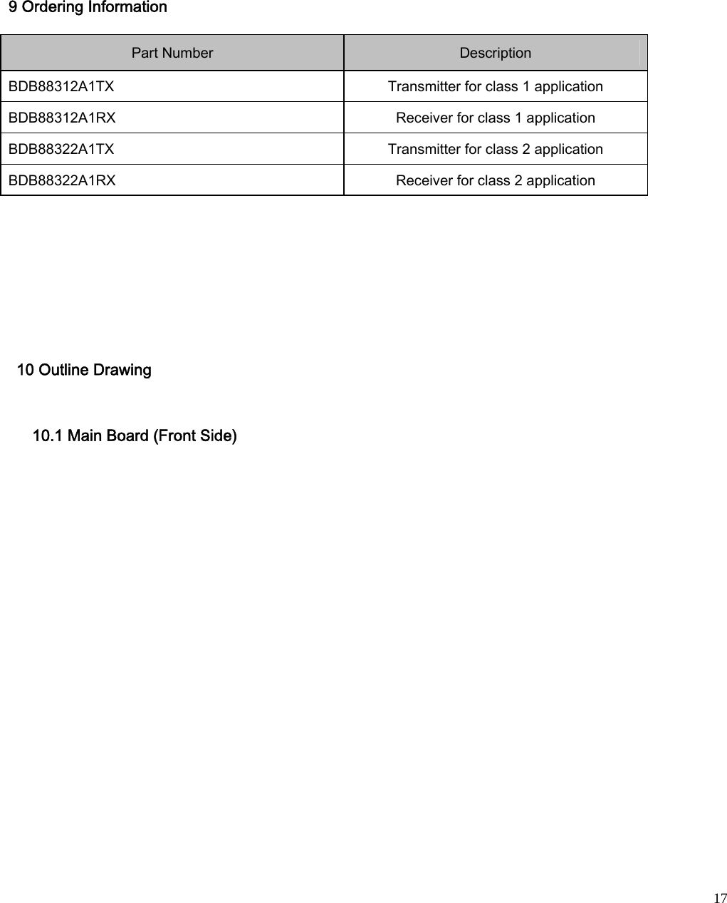
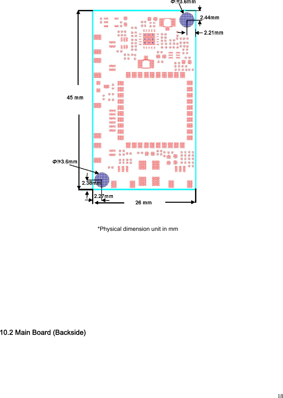
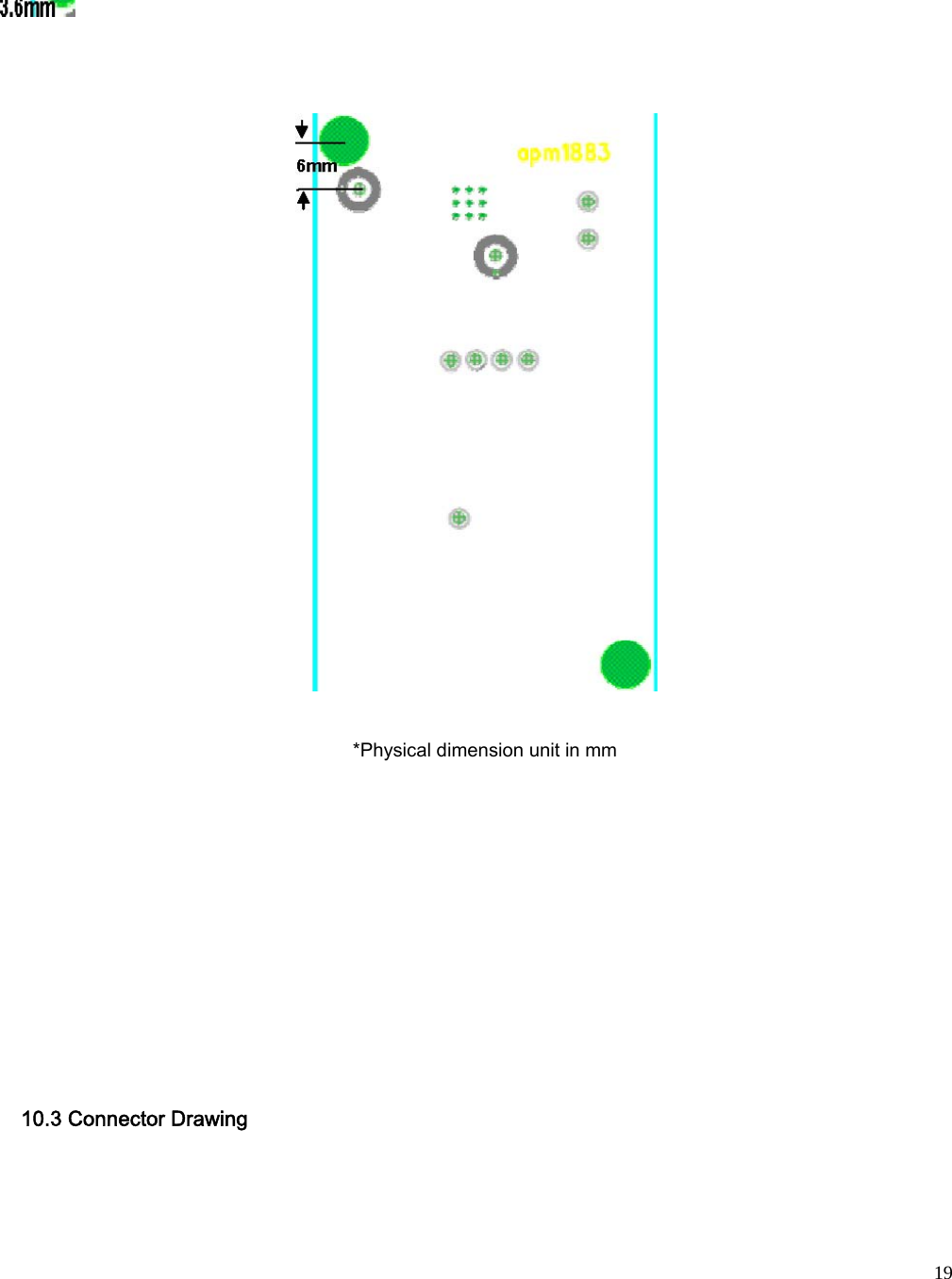
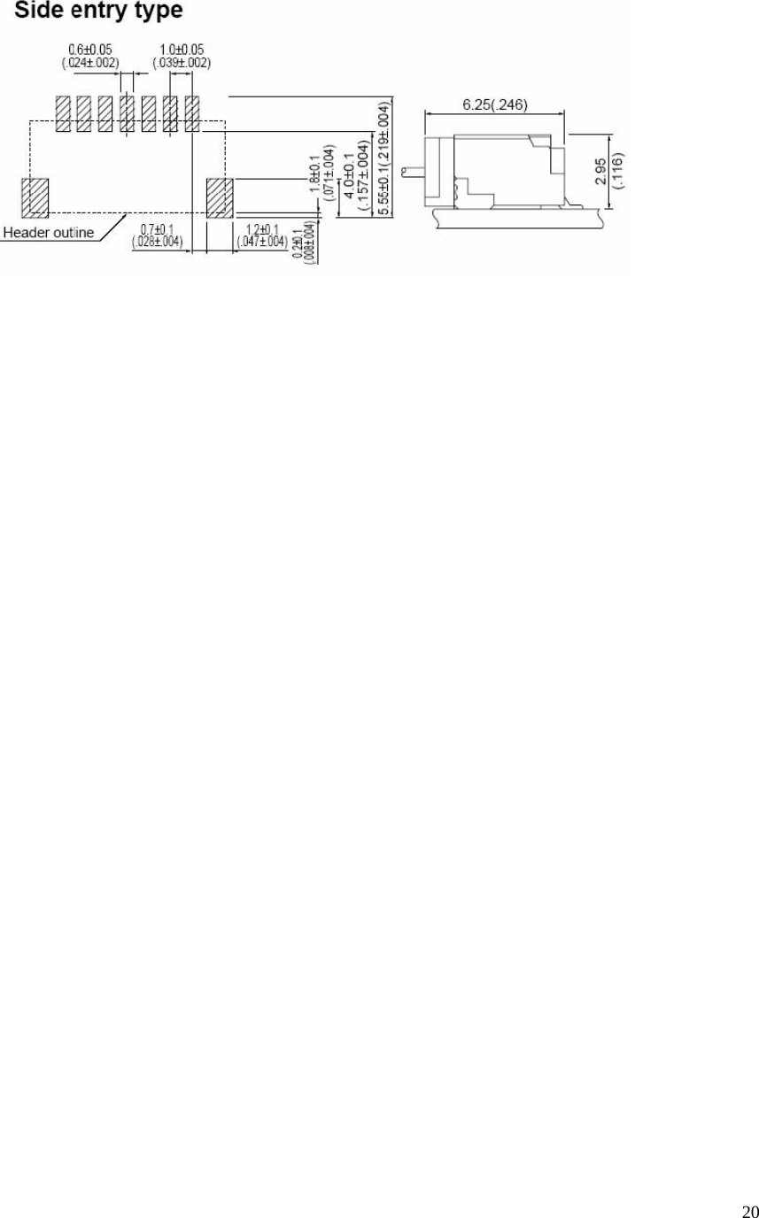
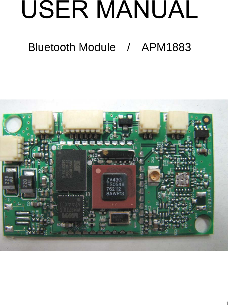
Juster APM1883 Bluetooth Module User Manual 1883
Juster Co., Ltd. Bluetooth Module 1883
UserManual.wiki
>
Juster
>
APM1883 User Manual
Manual
Navigation menu
Upload a User Manual
Namespaces
Wiki Guide
HTML
PDF
Info
Views
User Manual
Discussion / Help
Navigation
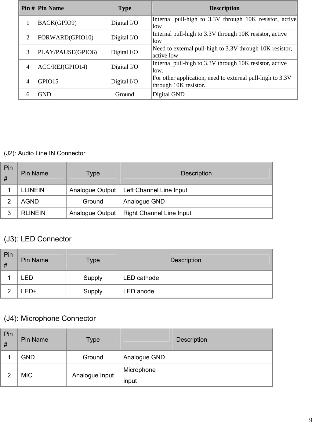
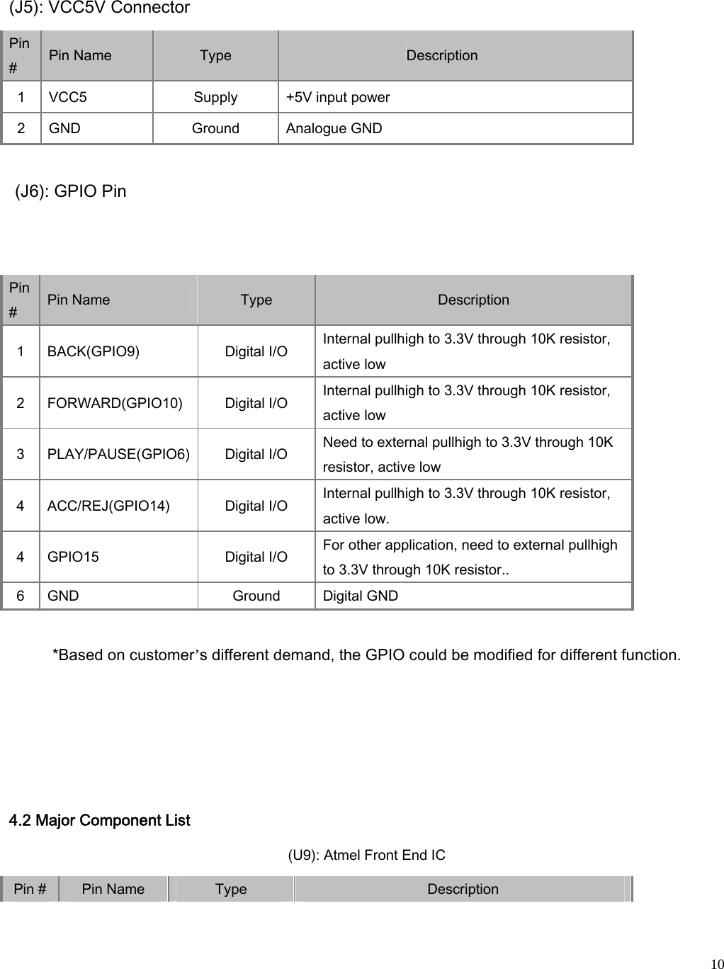
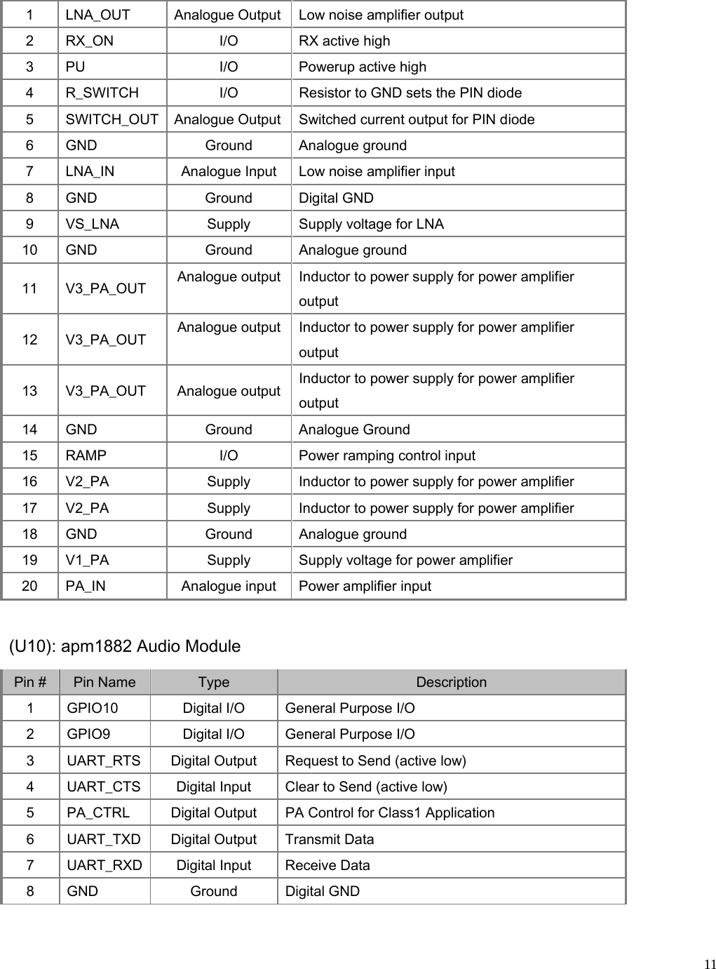
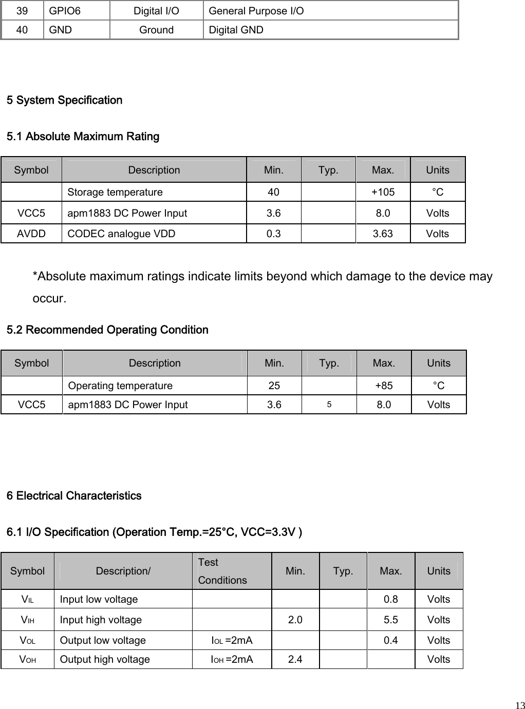
![129 ANT RF I/O 50 Ohm Rx/Tx Connection to Antenna 10 GND Ground Digital GND Pin # Pin Name Type Description 11 GPIO11 Digital I/O General Purpose I/O 12 GPIO12 Digital I/O General Purpose I/O 13 INT_0 Digital Input External interrupt [0] 14 VDD_USB Supply USB VDD 15 VDD_ DIG Supply Bluetooth Digital VDD 16 GPIO13 Digital I/O General Purpose I/O 17 GPIO14 Digital I/O General Purpose I/O 18 GPIO15 Digital I/O General Purpose I/O 19 GND Ground Digital GND 20 GND Ground Digital GND 21 GND Ground Digital GND 22 MODE Digital Input Mode Selection (16Mbit Flash Memory A19 Selection) 23 GND Ground Digital GND 24 VCC Supply Flash Memory VCC 25 GPIO0 Digital I/O General Purpose I/O (12MHz test point) 26 DVDD Supply CODEC Digital Core VDD 27 AVDD Supply CODEC Analogue VDD 28 LHPOUT Analogue Output Left Channel Headphone Output 29 RHPOUT Analogue Output Right Channel Headphone Output 30 MICBIAS Analogue Output Electric Microphone Bias 31 AGND Ground Analogue GND 32 MICIN Analogue Input Microphone Input (AC Coupled) 33 RLINEIN Analogue Input Right Channel Line Input (AC Coupled) 34 LLINEIN Analogue Input Left Channel Line Input (AC Coupled) 35 VDD_ANG Supply Bluetooth Analog VDD 36 VDD_VCO Supply Bluetooth VCO VDD 37 VDD_RF Supply Bluetooth RF VDD 38 RESET Digital Input Reset Input (Active Low for 5 ms); Schmitt Triggered](https://usermanual.wiki/Juster/APM1883/User-Guide-743323-Page-12.png)