Manual
1
USER MANUAL
Bluetooth Module / APM1883
2
TABLE OF CONTENTS
1. FCC Statement ………………………………………………………………….…….2
2. Description…………………………………………………………….……………….3
3. Set Steps……………………………………………………………………………….6
4. PIN ASSIGNMENT.…………………………………………………….……………..7
4.1 PIN DEFINITION………………………………………………………………….7
4.2 MAJOR COMPONENT LIST……………………………………………………10
5. SYSTEM SPECIFICATION………………………………………………………….12
5.1 ABSOLUTE MAXIMUM RATING……………………………………………….12
5.2 RECOMMENDED OPERATING CONDITION………………………………..13.
6. ELECTRICAL CHARACTERISTICS……………………………………………….13
6.1 I/O SPECIFICATION…………………………………………………………….13
6.2RF SPECIFICATION TEST SUMMARY……………………………………………..14
6.3 CURRENT CONSUMPTION TEST…………………………………………………..15
6.4 AUDIO SPECIFICATION………………….……………………………………16
7. LED STATUS…………………………………………………………………………16
8. CONNECTION (INQUIRY/PAIRING) TIME…………………………….…………16
9. ORDERING INFORMATION……………………………………………….………16
10. OUTLINE DRAWING………………………………………………………..………17
10.1 MAIN BOARD (FRONT SIDE)…………………………………..……………18
10.2 MAIN BOARD(BACKSIDE)…………………………………………………...18
10.3 CONNECTIOR DRAWING……………………………………………………19
11. FCC TO OEM installer…………………….………………….……………………..22
12. Label………………………..…………………………………………………………23
3
FCC Statement
This equipment complies with FCC radiation exposure limits set forth for an
uncontrolled environment. End users must follow the specific operating instructions
for satisfying RF exposure compliance. This transmitter must not be co-located or
operating in conjunction with any other antenna or transmitter. Notice: Any changes
or modification not expressly approved by the party responsible could void the user’s
authority to operate the device.
This device complies with part 15 of the FCC Rules. Operation is subject to the
following two conditions: (1) This device may not cause harmful interference, and (2)
this device must accept any interference received, including interference that may
cause undersired operation.
The Bluetooth Module allows a speakers with a communicate with other
Bluetooth-enabled devices. When used with the Bluetooth application software, it can
perform wireless network application such as information exchange, file transfer,
network access, dial-up networking, headset audio gateway, and so on.
4
General Description
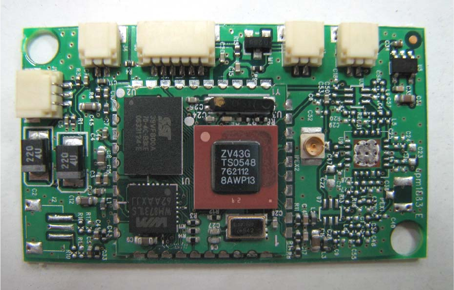
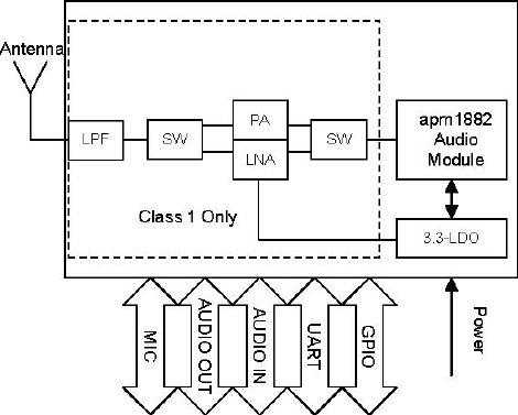
The apm1883 Bluetooth audio transceiver provides off-the-shelf wireless function
for class1 and class2 stereo audio application. It consists of apm1882 Bluetooth audio
module, PA/LNA, RF switch and LPF with a compact size of 45mm by 26mm for class1
solution. The apm1882 integrates Broadcom’s ZV4301 Bluetooth chip, Wolfson’s
WM8731 CODEC, crystal and Flash memory on a single module. It could be easily
embedded into audio system for Bluetooth wireless communication.
The specified profiles and firmware are pre-loaded into the built-in flash memory of
apm1882 module for Bluetooth audio transmission and receiving. The user could
update the firmware version by using the UART interface test point connect to host PC.
Features
�Compact size class1 and class2 Bluetooth audio transceiver: 45×26mm.
�Integrate apm1882 Bluetooth audio module, PA/LNA,
RF switch and LPF into one board for class1 solution.
�Compliant with Bluetooth specification V1.2.
�Low power modes available
�Easy to embed in Bluetooth audio System
�Class1 performance (with PA/LNA)
RF output power: < +20 dBm Receiver sensitivity: 85dBm @0.1%BER
�Class2 performance (without PA/LNA) RF output power: < +4 dBm Receiver
sensitivity: 80dBm @0.1%BER
5
Applications
� AV equipments
� Bluetooth stereo headphone or speaker which supports audio source switch
between stereo music and cellular phone call
� Bluetooth audio adaptor to transmit music from an analog source
Functional Block Diagram

6
Revision History
Date Release Author Description
29Jun06 1.0 Yushin/Baron Initial release
3. Setup Steps
Providing 5V to DC power J5
For LED indication please connect to J3
For remote control please using J6
For microphone input please connecting J4
For speaker use please connecting audio out to J1(BDB88312A1RX,
BDB88322A1RX only)
For audio transmit please connecting audio in to J2 (BDB88312A1TX,
BDB88322A1TX only)
IPEX1 is RF cable connector and is used for BDB88312A1TX, BDB88312A1RX
IPEX2 is RF cable connector and is used for BDB88322A1TX, BDB88322A1RX
7
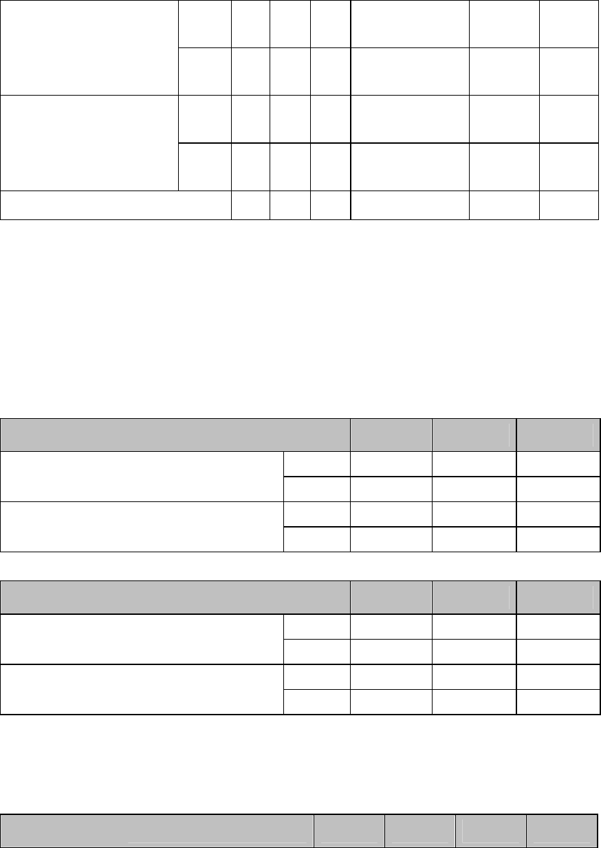
4. Pin Assignment
4.1 Pin Definition
(J1): Headphone Output Connector
Pin # Pin Name Type Description
1 LHPOUT Analogue Output Left Channel Headphone Output
2 AGND Ground Analogue GND
J5
J6
J3
J1: Headphone Output
For Receiver
U10
U9
For Class 1
IPEX 1
For Class 1
GPIO Pin
LED
DC Power Input
(Top View) (Bottom View)
UART Test Point
RF Test Point
For Class 1
J4
MIC Input
For Receiver
3.6mm
IPEX 2
For Class 2
J2: Audio Line In
For Transmitter
RF Test Point
For Class 2
VCC 5V
GND
UCTS URTS UTXD URXD
DC Test Point
: Connector & Device Pin 1 mark
8
Pin # Pin Name Type Description
3 RHPOUT Analogue Output
Right Channel
Headphoe Output
(J2): Audio Line IN Connector
Pin # Pin Name Type Description
1 LLINEIN Analogue Output Left Channel Line Input
2 AGND Ground Analogue GND
3 RLINEIN Analogue Output Right Channel Line Input
(J3):LED Connector
Pin # Pin Name Type Description
1 LED- Supply LED cathode
2 LED+ Supply LED anode
(J4):Microphone Connector
Pin # Pin Name Type Description
1 GND Ground Analogue GND
2 MIC Analogue Input Microphone input
(J5):VCC5V Connector
Pin # Pin Name Type Description
1 VCC5 Supply +5V input power
2 GND Ground Analogue GND
(J6):GPIO Pin
Pin # Pin Name Type Description
n

9
Pin # Pin Name Type Description
1 BACK(GPIO9) Digital I/O Internal pull-high to 3.3V through 10K resistor, active
low
2 FORWARD(GPIO10) Digital I/O Internal pull-high to 3.3V through 10K resistor, active
low
3 PLAY/PAUSE(GPIO6) Digital I/O Need to external pull-high to 3.3V through 10K resistor,
active low
4 ACC/REJ(GPIO14) Digital I/O Internal pull-high to 3.3V through 10K resistor, active
low.
4 GPIO15 Digital I/O For other application, need to external pull-high to 3.3V
through 10K resistor..
6 GND Ground Digital GND
(J2): Audio Line IN Connector
Pin
# Pin Name Type Description
1 LLINEIN Analogue Output Left Channel Line Input
2 AGND Ground Analogue GND
3 RLINEIN Analogue Output Right Channel Line Input
(J3): LED Connector
Pin
# Pin Name Type Description
1 LED Supply LED cathode
2 LED+ Supply LED anode
(J4): Microphone Connector
Pin
# Pin Name Type Description
1 GND Ground Analogue GND
2 MIC Analogue Input Microphone
input

10
(J5): VCC5V Connector
Pin
# Pin Name Type Description
1 VCC5 Supply +5V input power
2 GND Ground Analogue GND
(J6): GPIO Pin
Pin
# Pin Name Type Description
1 BACK(GPIO9) Digital I/O Internal pullhigh to 3.3V through 10K resistor,
active low
2 FORWARD(GPIO10) Digital I/O Internal pullhigh to 3.3V through 10K resistor,
active low
3 PLAY/PAUSE(GPIO6) Digital I/O Need to external pullhigh to 3.3V through 10K
resistor, active low
4 ACC/REJ(GPIO14) Digital I/O Internal pullhigh to 3.3V through 10K resistor,
active low.
4 GPIO15 Digital I/O For other application, need to external pullhigh
to 3.3V through 10K resistor..
6 GND Ground Digital GND
*Based on customer’s different demand, the GPIO could be modified for different function.
4.2 Major Component List
(U9): Atmel Front End IC
Pin # Pin Name Type Description

11
1 LNA_OUT Analogue Output Low noise amplifier output
2 RX_ON I/O RX active high
3 PU I/O Powerup active high
4 R_SWITCH I/O Resistor to GND sets the PIN diode
5 SWITCH_OUT Analogue Output Switched current output for PIN diode
6 GND Ground Analogue ground
7 LNA_IN Analogue Input Low noise amplifier input
8 GND Ground Digital GND
9 VS_LNA Supply Supply voltage for LNA
10 GND Ground Analogue ground
11 V3_PA_OUT Analogue output Inductor to power supply for power amplifier
output
12 V3_PA_OUT Analogue output Inductor to power supply for power amplifier
output
13 V3_PA_OUT Analogue output Inductor to power supply for power amplifier
output
14 GND Ground Analogue Ground
15 RAMP I/O Power ramping control input
16 V2_PA Supply Inductor to power supply for power amplifier
17 V2_PA Supply Inductor to power supply for power amplifier
18 GND Ground Analogue ground
19 V1_PA Supply Supply voltage for power amplifier
20 PA_IN Analogue input Power amplifier input
(U10): apm1882 Audio Module
Pin # Pin Name Type Description
1 GPIO10 Digital I/O General Purpose I/O
2 GPIO9 Digital I/O General Purpose I/O
3 UART_RTS Digital Output Request to Send (active low)
4 UART_CTS Digital Input Clear to Send (active low)
5 PA_CTRL Digital Output PA Control for Class1 Application
6 UART_TXD Digital Output Transmit Data
7 UART_RXD Digital Input Receive Data
8 GND Ground Digital GND

12
9 ANT RF I/O 50 Ohm Rx/Tx Connection to Antenna
10 GND Ground Digital GND
Pin # Pin Name Type Description
11 GPIO11 Digital I/O General Purpose I/O
12 GPIO12 Digital I/O General Purpose I/O
13 INT_0 Digital Input External interrupt [0]
14 VDD_USB Supply USB VDD
15 VDD_ DIG Supply Bluetooth Digital VDD
16 GPIO13 Digital I/O General Purpose I/O
17 GPIO14 Digital I/O General Purpose I/O
18 GPIO15 Digital I/O General Purpose I/O
19 GND Ground Digital GND
20 GND Ground Digital GND
21 GND Ground Digital GND
22 MODE Digital Input Mode Selection (16Mbit Flash Memory A19
Selection)
23 GND Ground Digital GND
24 VCC Supply Flash Memory VCC
25 GPIO0 Digital I/O General Purpose I/O (12MHz test point)
26 DVDD Supply CODEC Digital Core VDD
27 AVDD Supply CODEC Analogue VDD
28 LHPOUT Analogue Output Left Channel Headphone Output
29 RHPOUT Analogue Output Right Channel Headphone Output
30 MICBIAS Analogue Output Electric Microphone Bias
31 AGND Ground Analogue GND
32 MICIN Analogue Input Microphone Input (AC Coupled)
33 RLINEIN Analogue Input Right Channel Line Input (AC Coupled)
34 LLINEIN Analogue Input Left Channel Line Input (AC Coupled)
35 VDD_ANG Supply Bluetooth Analog VDD
36 VDD_VCO Supply Bluetooth VCO VDD
37 VDD_RF Supply Bluetooth RF VDD
38 RESET Digital Input Reset Input (Active Low for 5 ms); Schmitt Triggered

13
39 GPIO6 Digital I/O General Purpose I/O
40 GND Ground Digital GND
5 System Specification
5.1 Absolute Maximum Rating
Symbol Description Min. Typ. Max. Units
Storage temperature 40 +105 °C
VCC5 apm1883 DC Power Input 3.6 8.0 Volts
AVDD CODEC analogue VDD 0.3 3.63 Volts
*Absolute maximum ratings indicate limits beyond which damage to the device may
occur.
5.2 Recommended Operating Condition
Symbol Description Min. Typ. Max. Units
Operating temperature 25 +85 °C
VCC5 apm1883 DC Power Input 3.6 5 8.0 Volts
6 Electrical Characteristics
6.1 I/O Specification (Operation Temp.=25°C, VCC=3.3V )
Symbol Description/ Test
Conditions Min. Typ. Max. Units
VIL Input low voltage 0.8 Volts
VIH Input high voltage 2.0 5.5 Volts
VOL Output low voltage IOL =2mA 0.4 Volts
VOH Output high voltage IOH =2mA 2.4 Volts

14
IOL Output low current VOL =0.4V 2.2 mA
IOH Output high current VOH =2.4V 3.1 mA
II Input leakage current VI=3.3V or 0V 1 +1 Volts
0dB gain 20k 30k Ohms
RINLINE Line in input resistance 12dB gain 10k 15k Ohms
CINLINE Line in input capacitance 10 pF
RINMIC
Microphone input
resistance
10k Ohms
CINMIC
Microphone input
capacitance
10 pF
RL=32 Ohms 30 mW
PO Headphone output power RL=16 Ohms 50 mW
62 RF Specification Test Summary (Operation Temp.=25°C, VCC=3.3V)
Parameter Min Typ Max Bluetooth Spec. Unit Results
Class
1 +18 0 to +20 dBm Pass
Maximum RF transmit
power Class
2 +2 6 to +4 dBm Pass
Modulation index: �f1avg 140 165 175 140 < �f1avg <
175 kHz Pass
Modulation index: �f2max 115 172 > 115 kHz Pass
Modulation index: �f2avg / �f1avg 0.8 1.04 > 0.8 NA Pass
Initial carrier frequency accuracy 20 + 75 kHz Pass
Carrier frequency drift rate 11 20 < 20 kHz/50us Pass
Carrier frequency drift: one slot
packet 16 21 + 25 kHz Pass
Carrier frequency drift: three slot
packet 11 25 + 40 kHz Pass
Carrier frequency drift: five slot
packet 18 25 + 40 kHz Pass
15
Class
1 85 < 70 dBm Pass
Sensitivity – single slot
packets Class
2 80 < 70 dBm Pass
Class
1 85 < 70 dBm Pass
Sensitivity – multi slot
packets Class
2 80 < 70 dBm Pass
Maximum usable signal 20 0 > 20 dBm Pass
6.3 Current Consumption test (Operation Temp.=25°C, VCC=3.3V)
Transmitter Application Mode Average Maximum Units
Class 1 105 mA
Inquiry state Class 2 17 mA
Class 1 220 300 mA
Transmit DH(1,3,5) packets with PRBS9
payload (Transmitter) Class 2 86 120 mA
Headphone Application Mode Average Maximum Units
Class 1 17 mA
Inquiry scan Class 2 17 mA
Class 1 98 150 mA
Tester sends DH1 packets with PRBS9
payload to EUT Class 2 90 120 mA
6.4 Audio specification
Parameter Min Typ Max Unit

16
Sample rate 48 kHz
Noise level 60 dBA
DC input level 3.3 5 7 V
Input signal level
1 Vrms
Frequency
response
20 1k 20k Hz
S/N ratio 90 dB
Separation 90 dB
Hum & Noise
level
0.8 mV
7 LED Status
Operating State LED Blink Frequency
Inquiry scan Fast mode 10 Hz
Data
throughput
Slow mode 1.5 Hz
8. Connection (Inquiry/Pairing) Time
Operating State Typical Maximum Units
To connect a headset in first time 3 120 Sec.
To connect original headset after disconnection 3 8 Sec.
To connect different headset after disconnection 3 120 Sec.

17
9 Ordering Information
Part Number Description
BDB88312A1TX Transmitter for class 1 application
BDB88312A1RX Receiver for class 1 application
BDB88322A1TX Transmitter for class 2 application
BDB88322A1RX Receiver for class 2 application
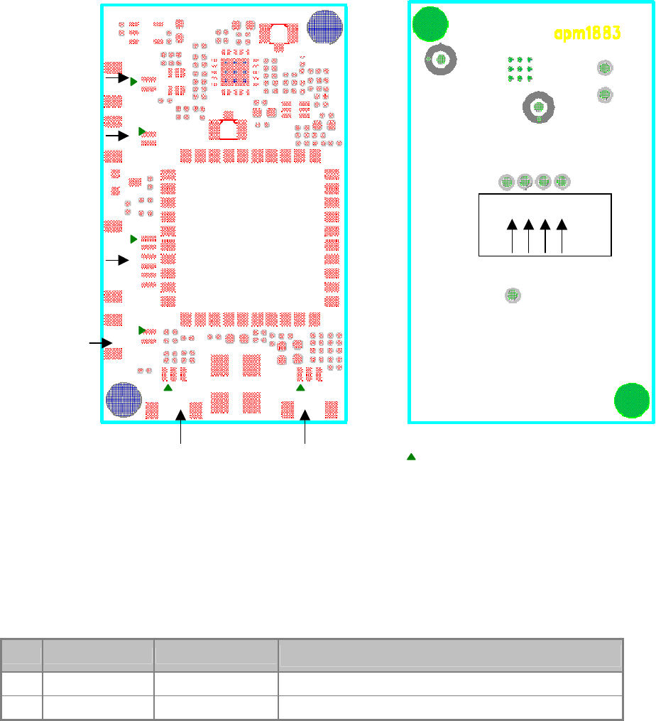
10 Outline Drawing
10.1 Main Board (Front Side)
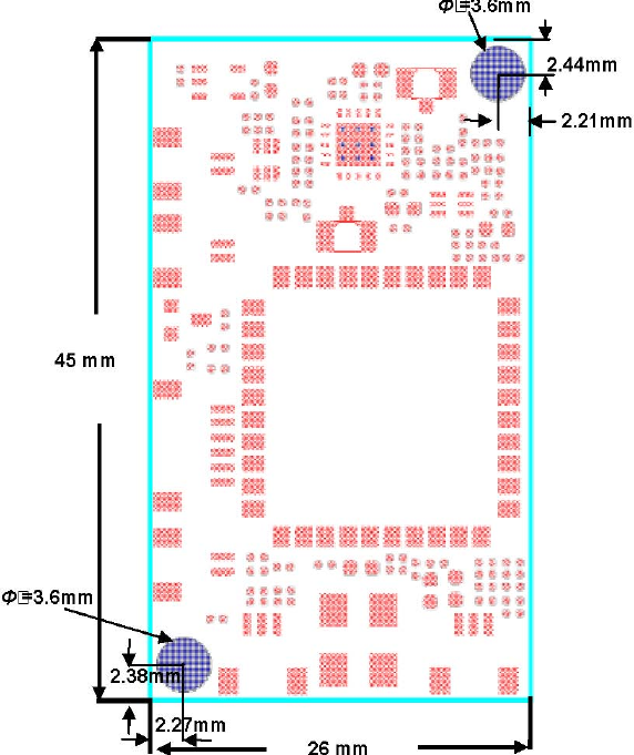
18
*Physical dimension unit in mm
10.2 Main Board (Backside)
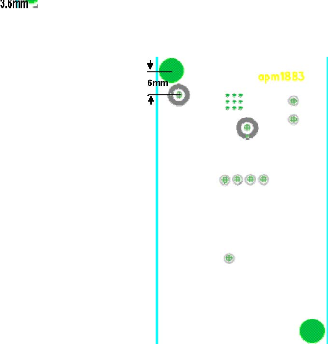
19
*Physical dimension unit in mm
10.3 Connector Drawing
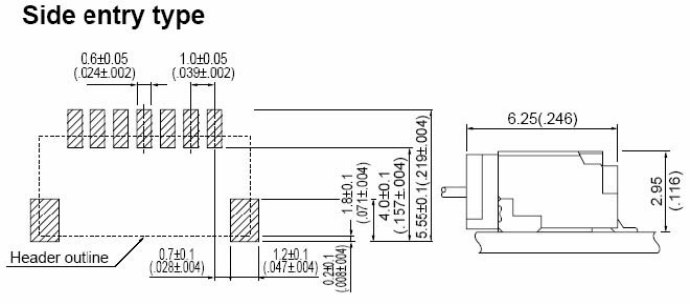
20
21
This equipment has been tested and found to comply with the limits for a Class B
digital device, pursuant to Part 15 of FCC Rules. These limits are designed to
provide reasonable protection against harmful interference in a residential
installation. This equipment generates, uses, and can radiate radio frequency
energy. If not installed and used in accordance with the instructions, However,
there is no guarantee that interference will not occur in a particular installation.
If this equipment does cause harmful interference to radio or television reception,
which can be determined by tuning the equipment off and on, the user is
encouraged to try and correct the interference by one or more of the following
measures:
- Reorient or relocate the receiving antenna
- Increase the distance between the equipment and the receiver.
- Connect the equipment to outlet on a circuit different from that to which the
receiver is connected.
- Consult the dealer or an experienced radio/TV technician for help.
Information for OEM integrator The OEM integrator has to be aware not to
provide information to the end user regarding how to install or remove this RF
module in the user manual of the end product. The user manual which is
provided by OEM integrators for end users must include the following information
in a prominent location. “To comply with FCC RF exposure compliance
requirements, the antenna used for this transmitter must be installed to provide a
separation distance of at least 20 cm from all persons and must not be
co-located or operating in conjunction with any other antenna or transmitter.”
Label for end product must include “ Contains FCC ID: SETAPM1883 ” or “ A RF
transmitter inside, FCC ID: SETAPM1883 ”.
TO OEM installer:
1. FCC ID label on the final system must be labeled with “Contains FCC ID:
22
SETAPM1883”
2. In the user manual, final system integrator must be ensure that there is no
instruction provided in the user manual to install or remove the speakers.
3. Audio module must be installed and used in strict accordance with the
manufacturer’s instruction as described in the user documentation that comes
with the product.
This device complies with the following radio frequency and safety standards.
The user manual of the final host system must contain the following statements:
USA-Federal Communications Commission (FCC)
This equipment has been tested and found to comply with the limits for a Class B
digital device, pursuant to Part 15 of FCC Rules. These limits are designed to
provide reasonable protection against harmful interference in a residential
installation. This equipment generates, uses, and can radiate radio frequency
energy. If not installed and used in accordance with the instructions, However,
there is no guarantee that interference will not occur in a particular installation.
If this equipment does cause harmful interference to radio or television reception,
which can be determined by tuning the equipment off and on, the user is
encouraged to try and correct the interference by one or more of the following
measures:
- Reorient or relocate the receiving antenna
- Increase the distance between the equipment and the receiver.
- Connect the equipment to outlet on a circuit different from that to which the
receiver is connected.
- Consult the dealer or an experienced radio/TV technician for help.

23
Any changes or modifications not expressly approved by the party responsible
for compliance could void the user’s authority to operate the equipment.
This device complies with part 15 of the FCC Rules. Operation is subject to the
following two conditions: (1) This device may not cause harmful interference, and
(2) this device must accept any interference received, including interference that
may cause undesired operation.
Any changes or modifications not expressly approved by the party responsible
for compliance could void the user’s authority to operate the equipment.
Caution: Exposure to Radio Frequency Radiation.
This device must not be co-located or operating in conjunction with any other
antenna or transmitter.
12. Label
FCC IDENTIFIER: SETAPM1883
Name of Grantee: Juster Co., Ltd.
Equipment Class: Part 15
Bluetooth Module