Kyocera KWC-M200 Transmitter Module User Manual 82 M8862 1
Kyocera Communications, Inc Transmitter Module 82 M8862 1
UserManual.wiki
>
Kyocera
>
KWC-M200 User Manual
>
manual part 4
Contents
1.
user guide1
2.
user guide2
3.
manual insert for antenna
4.
antenna information
5.
user manual part 1
6.
user manual part 2
7.
user manual part 3
8.
manual part 1
9.
manual part 2
10.
manual part 3
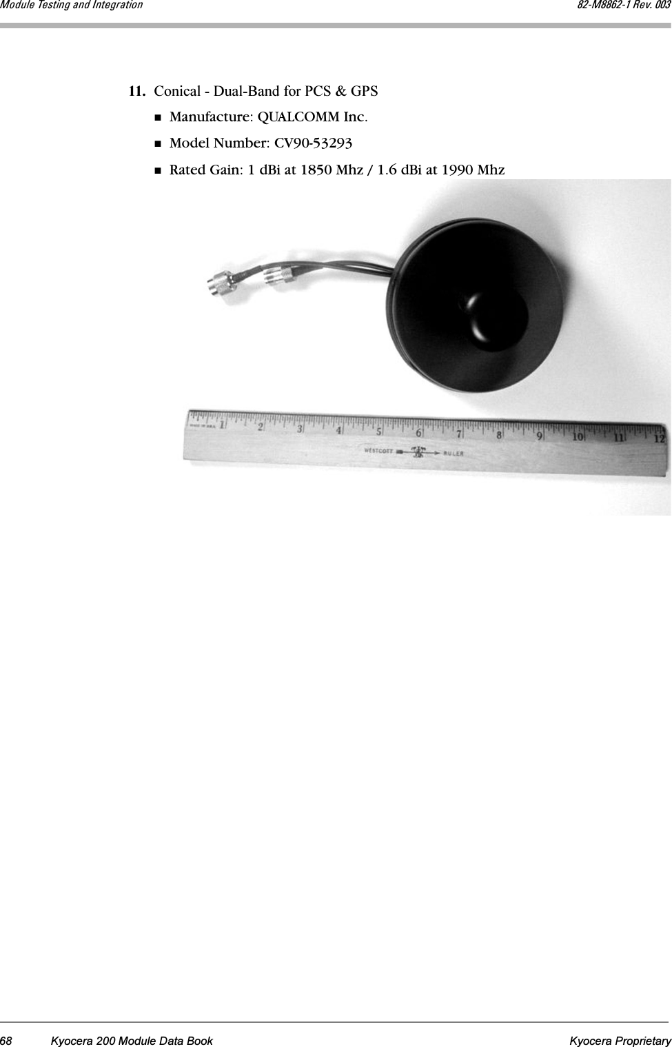
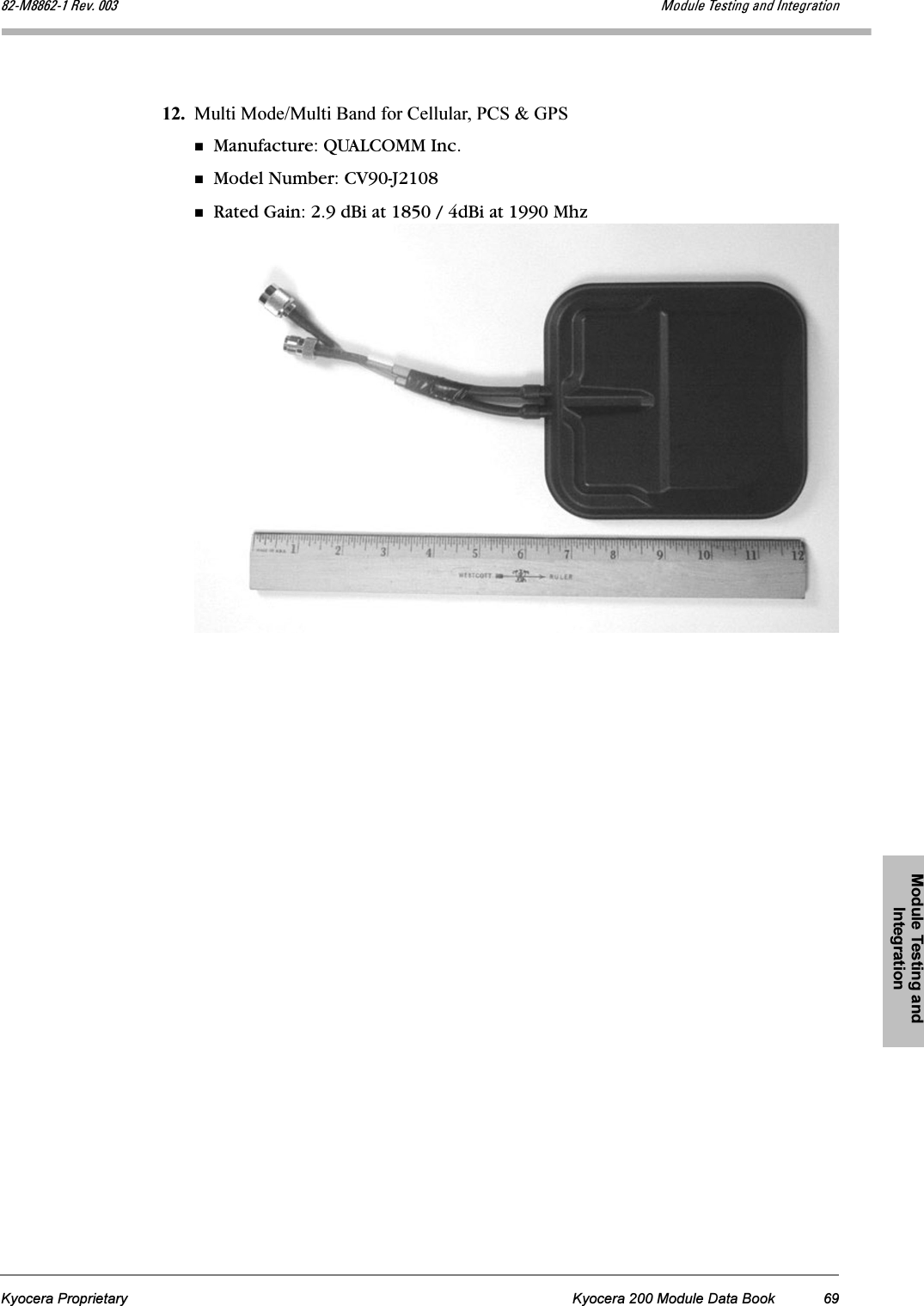
11.
manual part 4
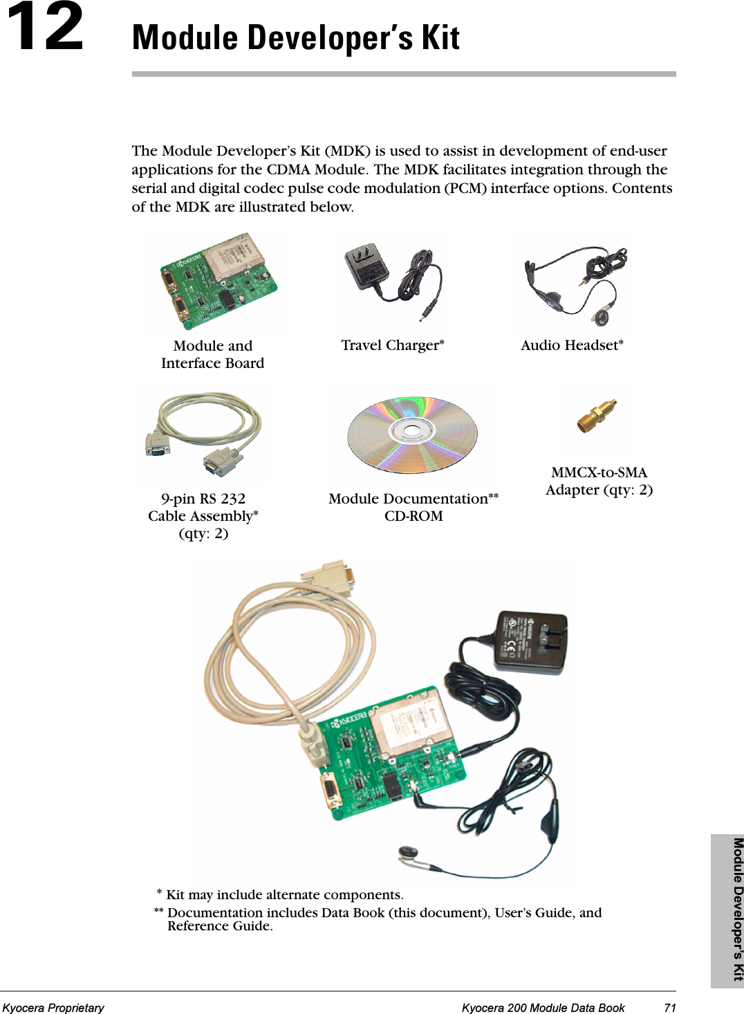
12.
User Manual
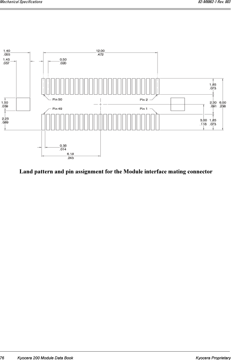
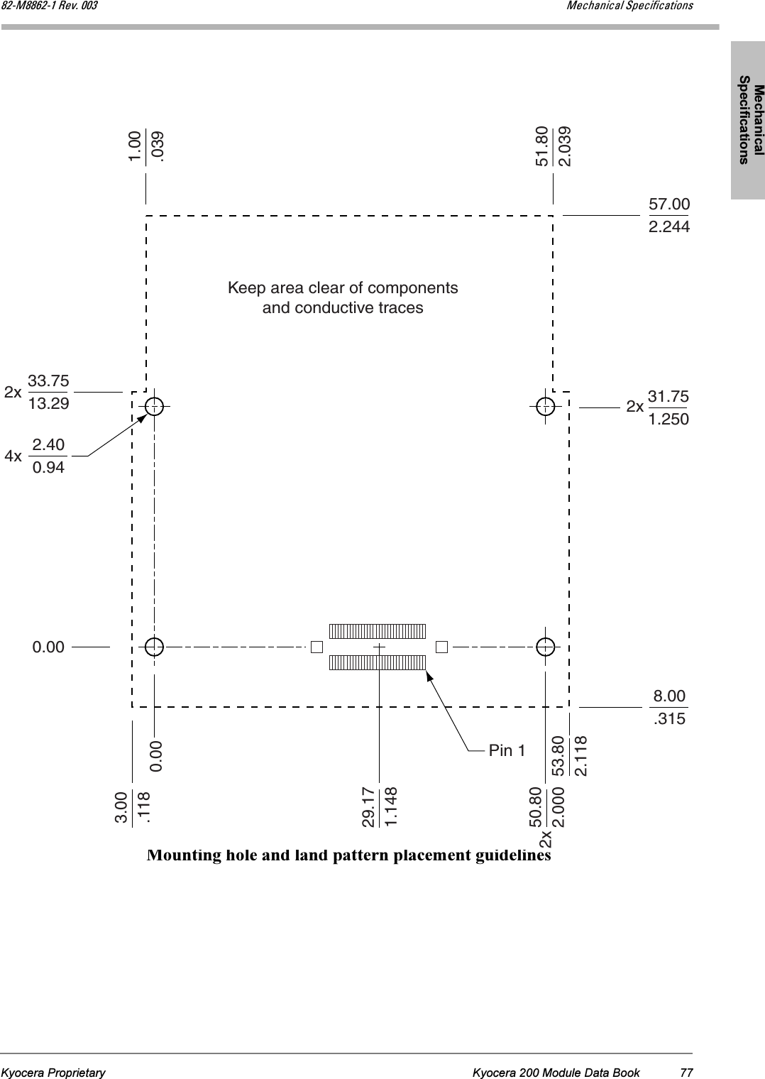
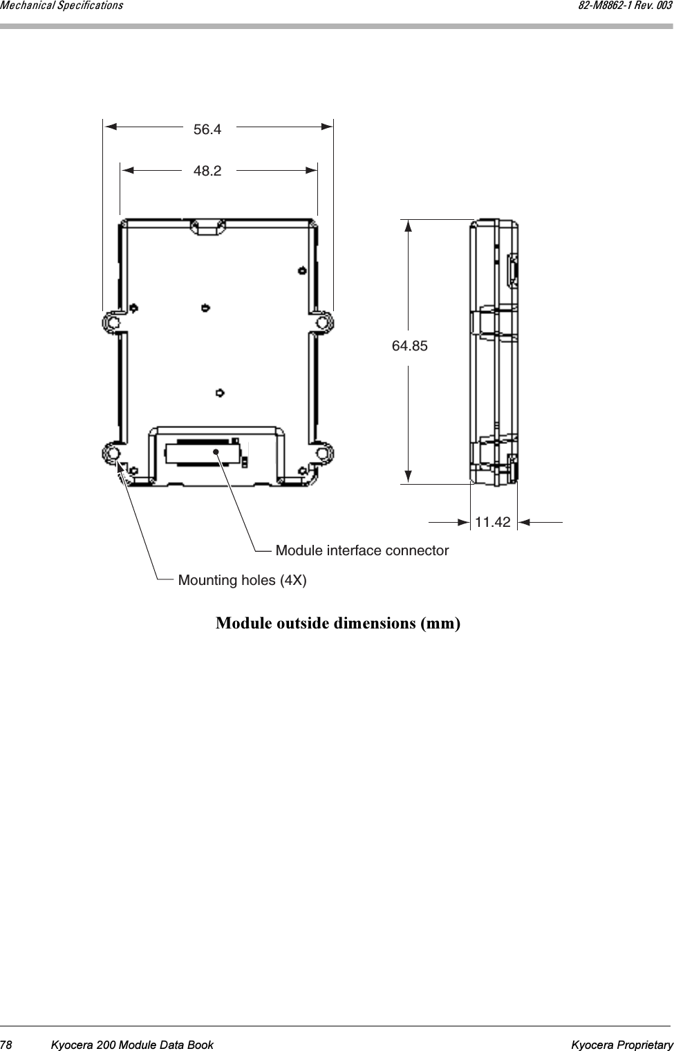
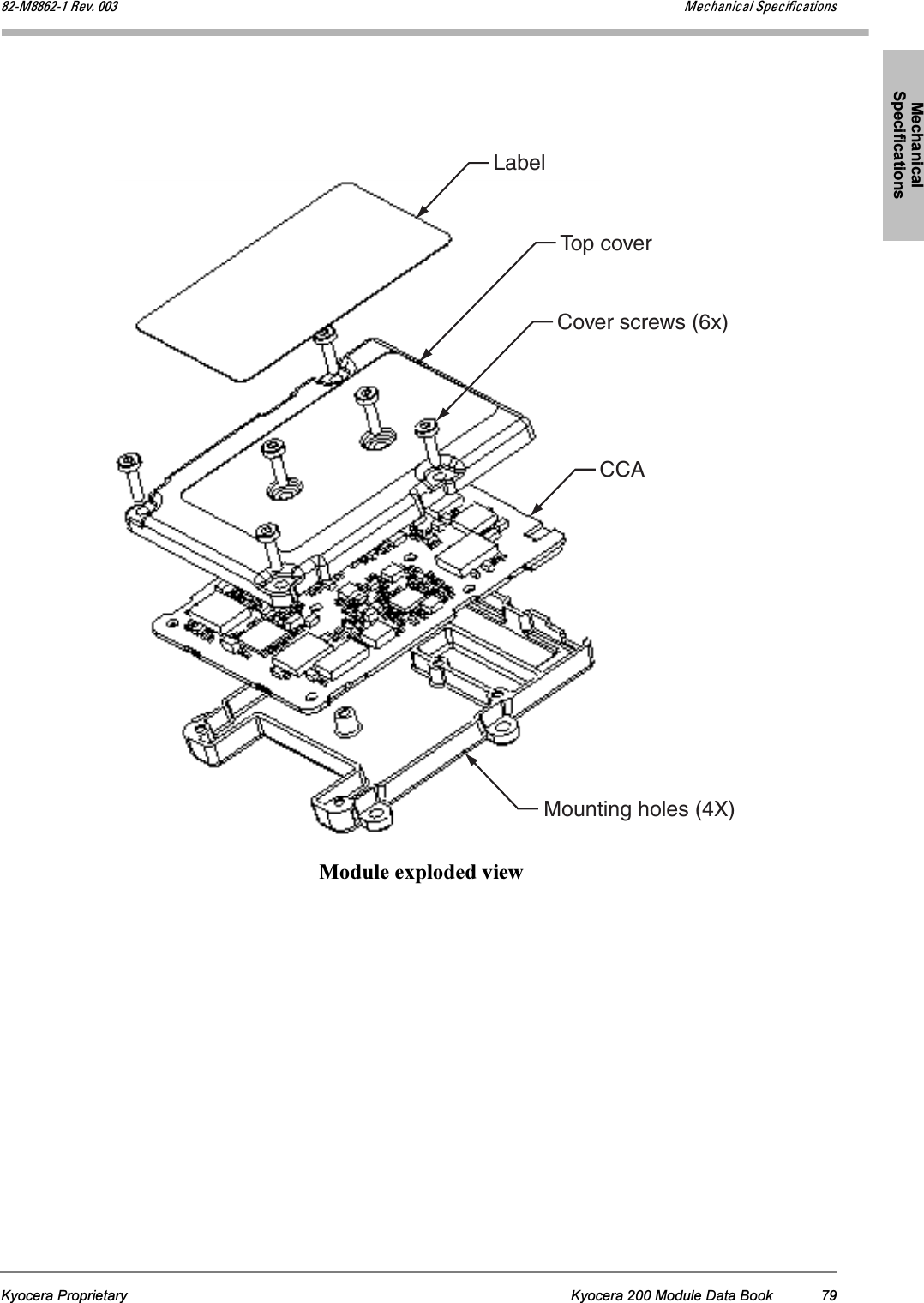
manual part 4
Navigation menu
Upload a User Manual
Namespaces
Wiki Guide
HTML
PDF
Info
Views
User Manual
Discussion / Help
Navigation