Kyocera KWC-M200 Transmitter Module User Manual 82 M8862 1
Kyocera Communications, Inc Transmitter Module 82 M8862 1
Kyocera >
Contents
manual part 4
68 Kyocera 200 Module Data Book Kyocera Proprietary
jçÇìäÉ=qÉëíáåÖ=~åÇ=fåíÉÖê~íáçå UOJjUUSOJN=oÉîK=MMP
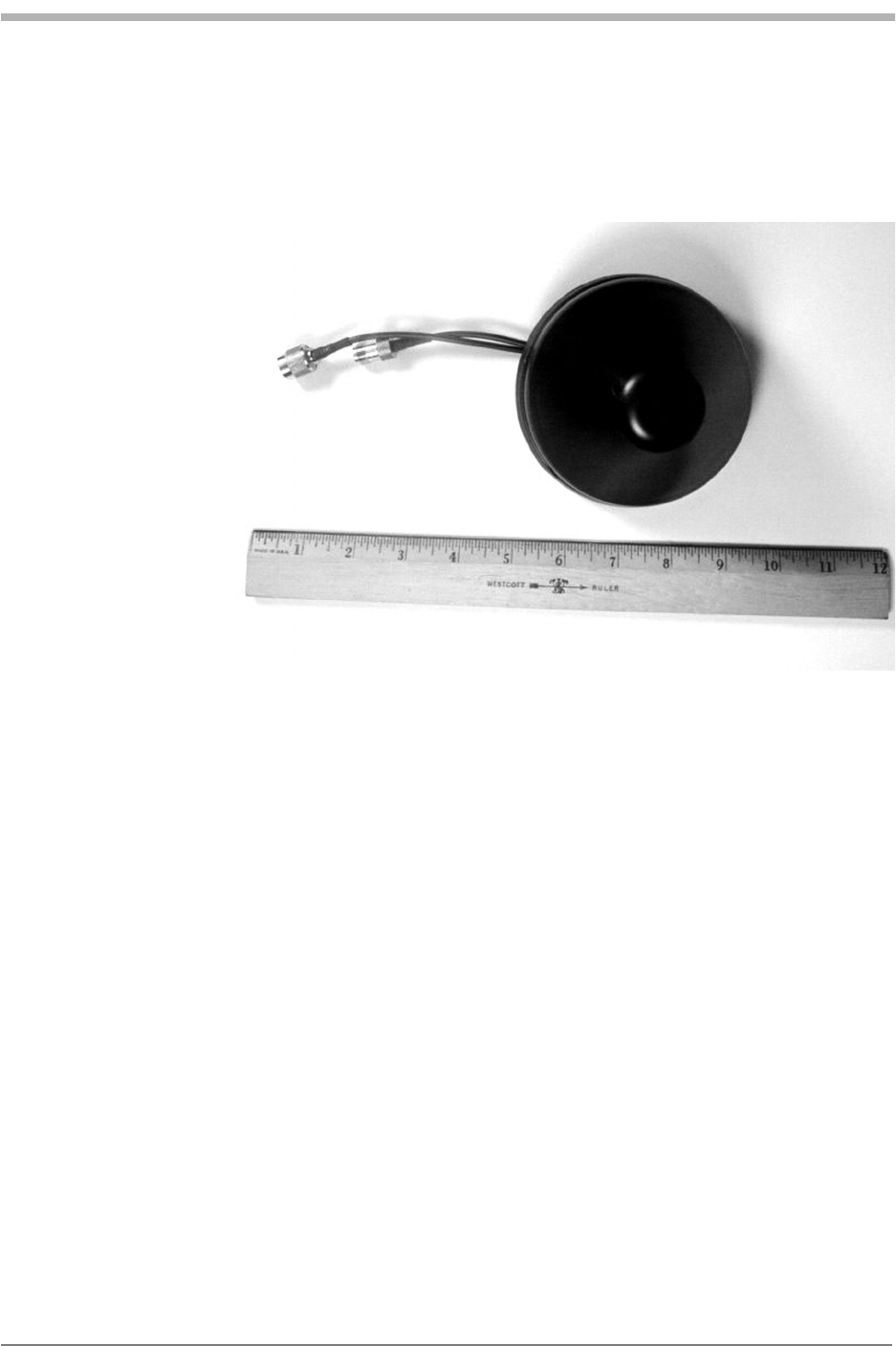
11. Conical - Dual-Band for PCS & GPS
Manufacture: QUALCOMM Inc.
Model Number: CV90-53293
Rated Gain: 1 dBi at 1850 Mhz / 1.6 dBi at 1990 Mhz
Module Testing and
Integration
Kyocera Proprietary Kyocera 200 Module Data Book 69
UOJjUUSOJN=oÉîK=MMP jçÇìäÉ=qÉëíáåÖ=~åÇ=fåíÉÖê~íáçå
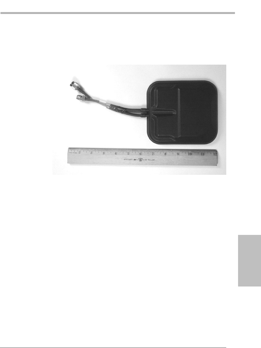
12. Multi Mode/Multi Band for Cellular, PCS & GPS
Manufacture: QUALCOMM Inc.
Model Number: CV90-J2108
Rated Gain: 2.9 dBi at 1850 / 4dBi at 1990 Mhz

70 Kyocera 200 Module Data Book Kyocera Proprietary
jçÇìäÉ=qÉëíáåÖ=~åÇ=fåíÉÖê~íáçå UOJjUUSOJN=oÉîK=MMP
c~Åíçêó=íÉëíë
Each Module undergoes functional testing per specifications using the RF test
connector. No radiated tests are performed. The 50 ohm coaxial RF interfaces are
verified. The manufactured end item needs to be verified for functionality of the
antenna system and audio circuits if used.
oÉÖ~êÇáåÖ=ÇÉîÉäçéãÉåí=~åÇ=íÉëíáåÖ=çÑ=lbj=ÇÉîáÅÉ=ìëáåÖ=jçÇìäÉW
OEM must follow standards for voice and data as indicated by TIA.
OEM must follow standards for AT commands to send data to the Module/phone.
OEM may require constant activation of device by desired carrier for ongoing
testing.
oÉÖ~êÇáåÖ=ÅÉêíáÑáÅ~íáçå=çÑ=ÇÉîáÅÉ=çå=Å~êêáÉêDë=åÉíïçêâ=Ñçê=rKpK=ã~êâÉíW
Upon accepting the Module as a tested component to the OEM’s device, the
carrier provides direction to the OEM as to further testing that may be required
on the OEM’s part.
Please note that service providers may require the OEM’s product to pass some
basic over-the-air testing before it can be active on a provider’s network. This will
ensure the service provider that the network will not be adversely affected
during an OEM’s product development.
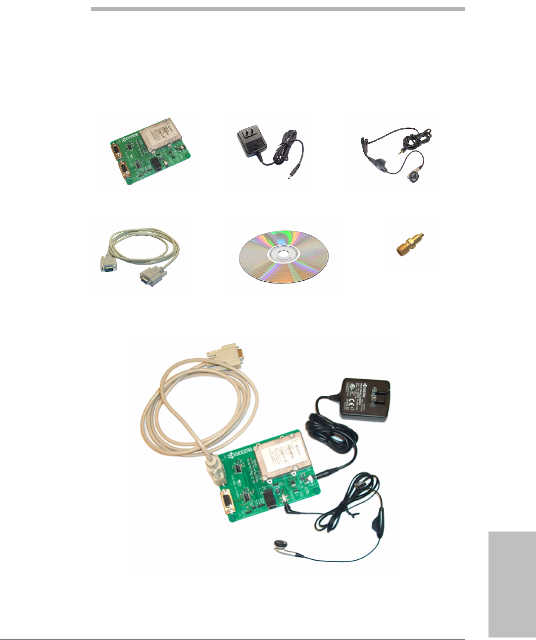
Module Developer’s Kit
Kyocera Proprietary Kyocera 200 Module Data Book 71
NO
jçÇìäÉ=aÉîÉäçéÉêÛë háí
The Module Developer’s Kit (MDK) is used to assist in development of end-user
applications for the CDMA Module. The MDK facilitates integration through the
serial and digital codec pulse code modulation (PCM) interface options. Contents
of the MDK are illustrated below.
Module and Travel Charger* Audio Headset*
9-pin RS 232
Cable Assembly*
Module Documentation**
CD-ROM
MMCX-to-SMA
Adapter (qty: 2)
* Kit may include alternate components.
Interface Board
(qty: 2)
** Documentation includes Data Book (this document), User’s Guide, and
Reference Guide.

72 Kyocera 200 Module Data Book Kyocera Proprietary
jçÇìäÉ=aÉîÉäçéÉêÛë háí UOJjUUSOJN=oÉîK=MMP
It should be clearly understood that the software in the MDK (specifically, the
code in the Kyocera 200 Module User’s Guide, 82-M8863-1) is provided for
sample purposes only. The MDK software is not warranted as the basis for a
deployed implementation.

Warranty and Product
Support
Kyocera Proprietary Kyocera 200 Module Data Book 73
NP
t~êê~åíó=~åÇ=mêçÇìÅí=pìééçêí
The KWC CDMA Module Developer’s Kit arrives having been tested as described
in the Module Testing & Integration chapter. Testing should be duplicated at the
integrator’s/customer’s facility. KWC can provide advice as to the type of test
equipment needed.
This Module testing should be separate from the testing to be performed on the
end product (with the Module installed). KWC offers a warranty for the CDMA
Module, from the date of shipment from KWC’s facility. This warranty provides
the customer with a remedy for defective Modules within the warranty period
and subject to all other warranty provisions.
KWC requests that the integrator retain several Modules as backup in case of
failure. It is assumed that you maintain a first level of returned Module testing in
your QA department prior to returning the Module to KWC. This alleviates the
question of whether the failure is in the Module or the end product. “No trouble
found” (NTF) occurrences on Modules returned to KWC will result in fees. KWC
reserves the right, at its own discretion, to repair, replace, or issue a trade credit
for any defective Module under warranty.
Warranty repair excludes warranty claims on products that have been subject to
misuse, neglect, improper storage or installation, or that have been repaired,
modified, or altered by a facility other than a KWC-authorized service center or a
KWC-certified repair center. In all cases, the final testing of the KWC line is the
sole controlling determination of Module performance.

74 Kyoera 200 Module Data Book Kyocera Proprietary
t~êê~åíó=~åÇ=mêçÇìÅí=pìééçêí UOJjUUSOJN=oÉîK=MMP

Mechanical
Specifications
Mechanical
Specifications
Mechanical
Specifications
Mechanical
Specifications
Mechanical
Specifications
Kyocera Proprietary Kyocera 200 Module Data Book 75
NQ
jÉÅÜ~åáÅ~ä=péÉÅáÑáÅ~íáçåë
j~íáåÖ=ÅçååÉÅíçêë
The following connectors mate with the Module.
Module RF Connector Mate
Standard MMCX plug, available from
several manufacturers including Amp,
Radiall, and Telegartner
Module Interface Connector Mate
Manufacturer: MOLEX Inc., www.molex.com
Manufacturer’s Part Number: 54230-0509
Kyocera MCN: 449-24545-0509
54230-0509 is the tape and reel version with only a fitting nail/solder tab for
retention. 54230-0508 is the tape and reel version with fitting nail and pcb peg
(goes into the pcb and helps pick and place alignment). Although the -0509 is not
on the Molex Web site, it is available.
Parts can be ordered based on the manufacturer’s part number, not Kyocera’s
internal MCN (Material Control Number).
Other suppliers for this part are:
eeParts, Inc., http://www.eeparts.com
1150 Hayden Dr, Ste 100
Carrolton, TX 75006
Phone: 469-574-2333/Fax: 469-574-2389
Sager Electronics, http://www.sager.com
97 Libbey Industrial Pkwy
Weymouth, MA 02189
Phone: 800-SAGER-800
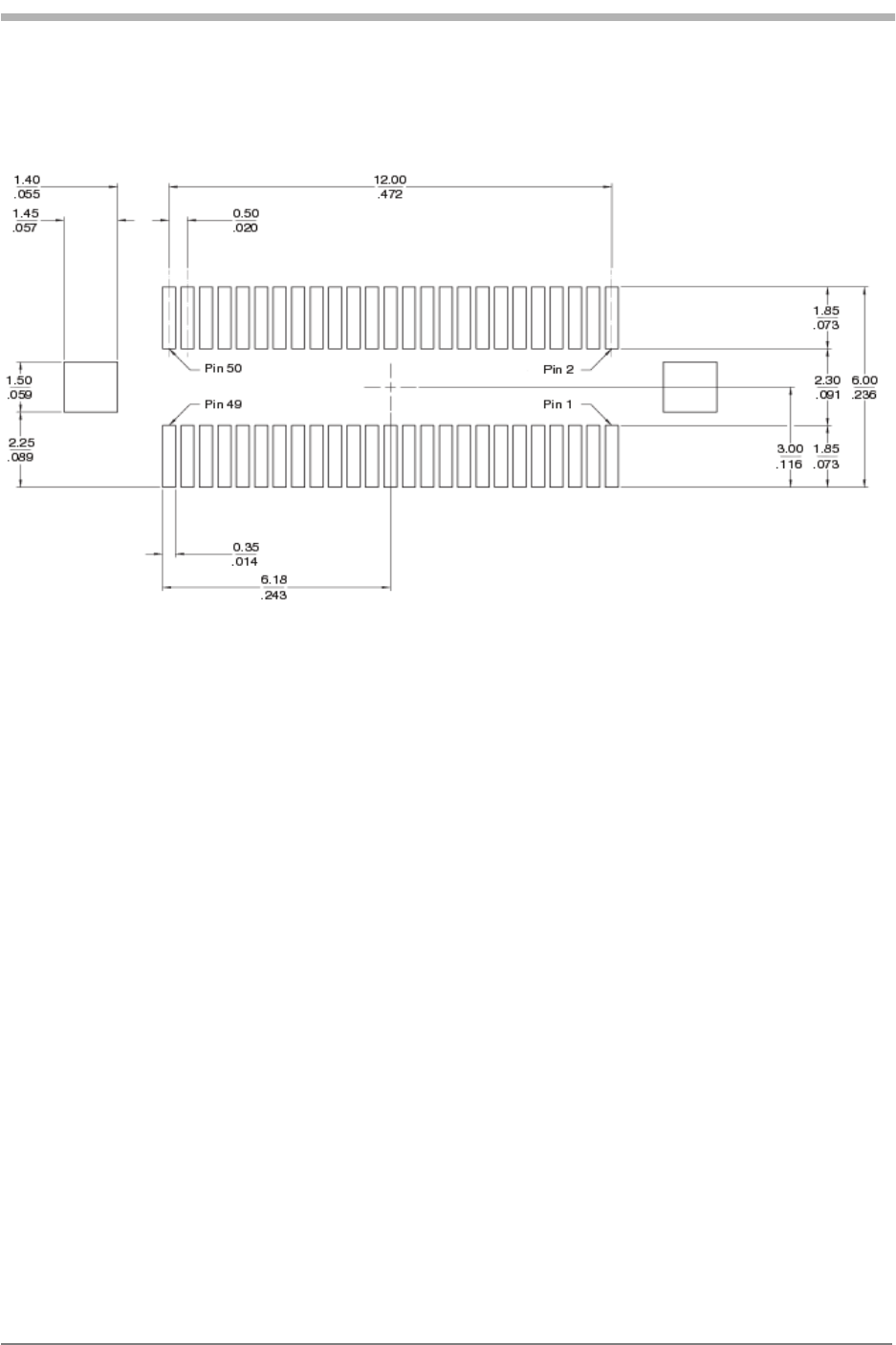
aê~ïáåÖë
The following technical drawings are included in this chapter:
Land pattern and pin assignment for Module interface mating connector
Mounting hole and land pattern placement guidelines with recommended
mounting hardware
Module overall dimensioned drawing
Module exploded view
76 Kyocera 200 Module Data Book Kyocera Proprietary
jÉÅÜ~åáÅ~ä=péÉÅáÑáÅ~íáçåë UOJjUUSOJN=oÉîK=MMP
Land pattern and pin assignment for the Module interface mating connector
Mechanical
Specifications
Mechanical
Specifications
Mechanical
Specifications
Mechanical
Specifications
Mechanical
Specifications
Kyocera Proprietary Kyocera 200 Module Data Book 77
UOJjUUSOJN=oÉîK=MMP jÉÅÜ~åáÅ~ä=péÉÅáÑáÅ~íáçåë
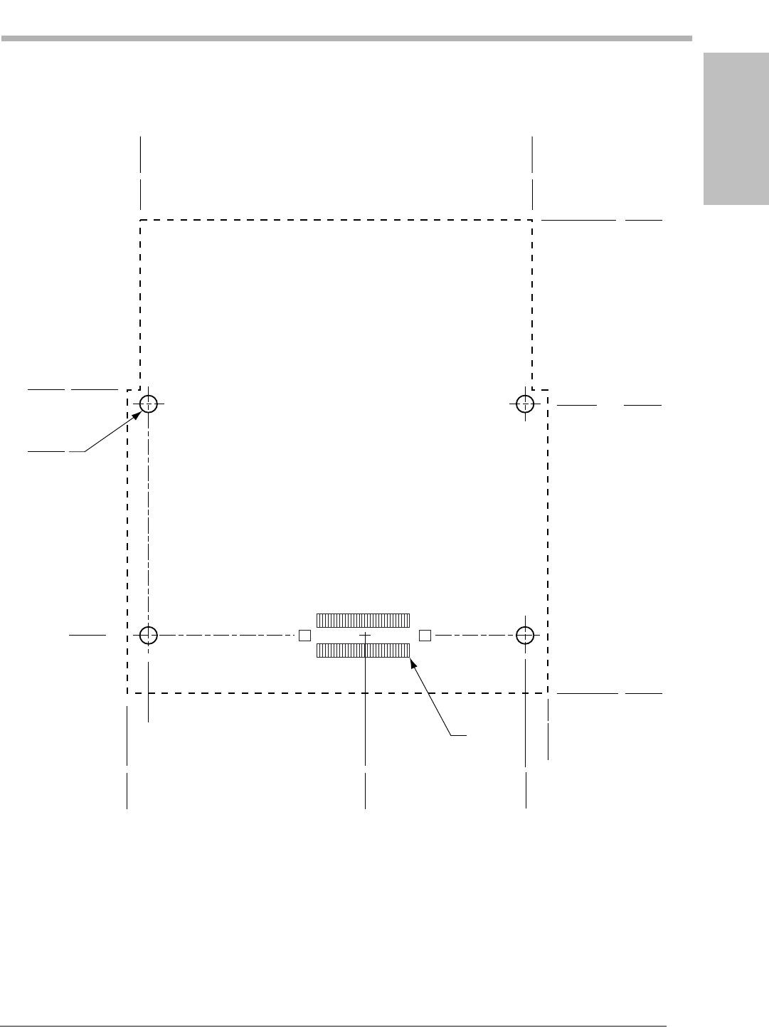
Mounting hole and land pattern placement guidelines
0.00
Keep area clear of components
and conductive traces
4x
Pin 1
2.40
0.94
2x 2x
33.75
13.29
57.00
2.244
8.00
.315
1.00
.039
51.80
2.039
31.75
1.250
2x 50.80
2.000 53.80
2.118
29.17
1.148
3.00
.118 0.00
78 Kyocera 200 Module Data Book Kyocera Proprietary
jÉÅÜ~åáÅ~ä=péÉÅáÑáÅ~íáçåë UOJjUUSOJN=oÉîK=MMP
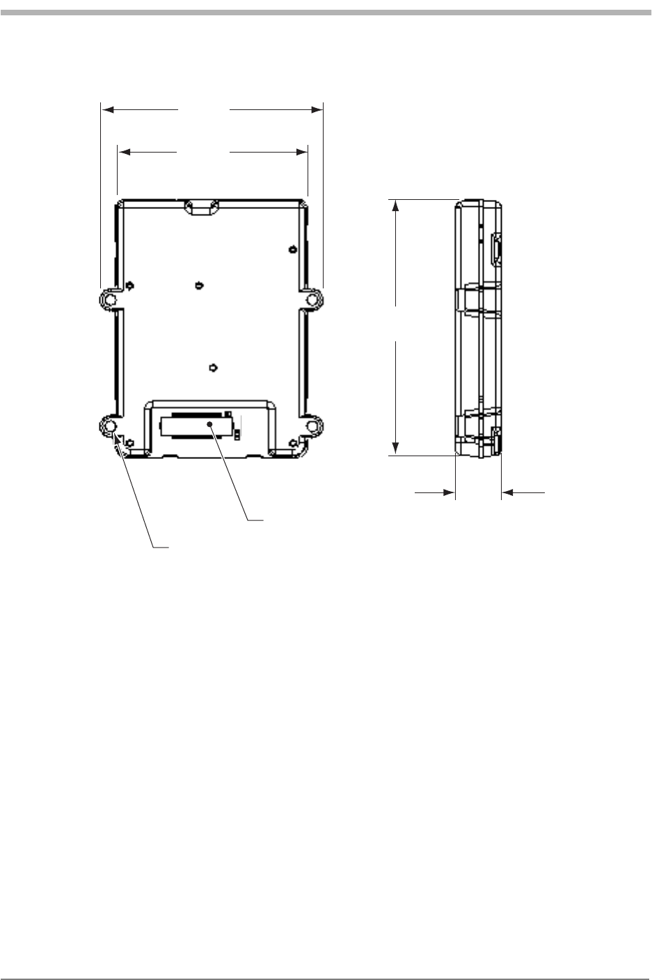
Module outside dimensions (mm)
Mounting holes (4X)
Module interface connector
56.4
48.2
64.85
11.42
Mechanical
Specifications
Mechanical
Specifications
Mechanical
Specifications
Mechanical
Specifications
Mechanical
Specifications
Kyocera Proprietary Kyocera 200 Module Data Book 79
UOJjUUSOJN=oÉîK=MMP jÉÅÜ~åáÅ~ä=péÉÅáÑáÅ~íáçåë
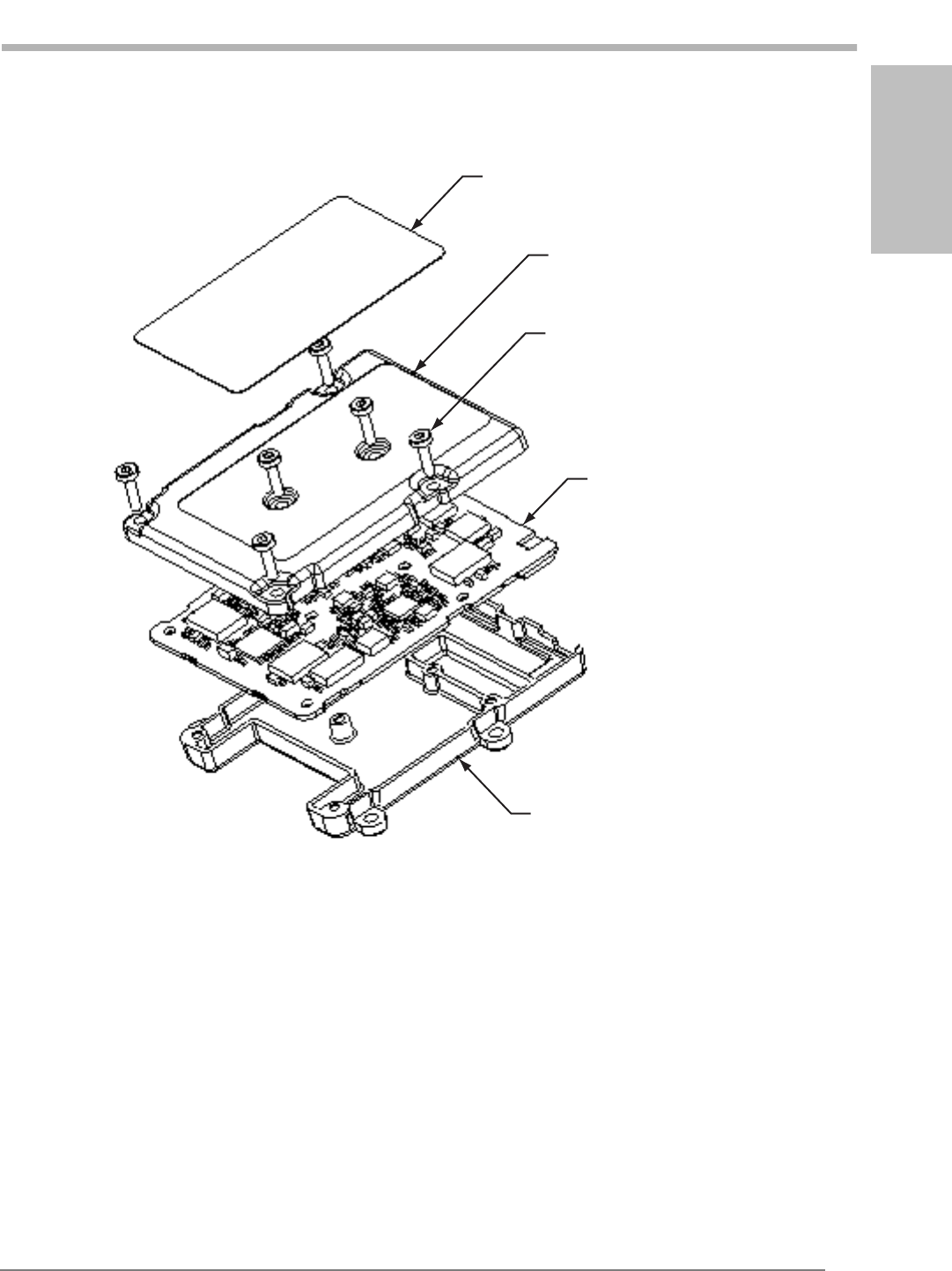
Module exploded view
Mounting holes (4X)
Label
Top cover
Cover screws (6x)
CCA

80 Kyocera 200 Module Data Book Kyocera Proprietary
jÉÅÜ~åáÅ~ä=péÉÅáÑáÅ~íáçåë UOJjUUSOJN=oÉîK=MMP
Assignments and Signal
Definitions
Assignments and Signal
Definitions
Assignments and Signal
Definitions
Assignments and Signal
Definitions
Assignments and Signal
Definitions
Kyocera Proprietary Kyocera 200 Module Data Book 81
NR
^ëëáÖåãÉåíë=~åÇ=páÖå~ä=aÉÑáåáíáçåë
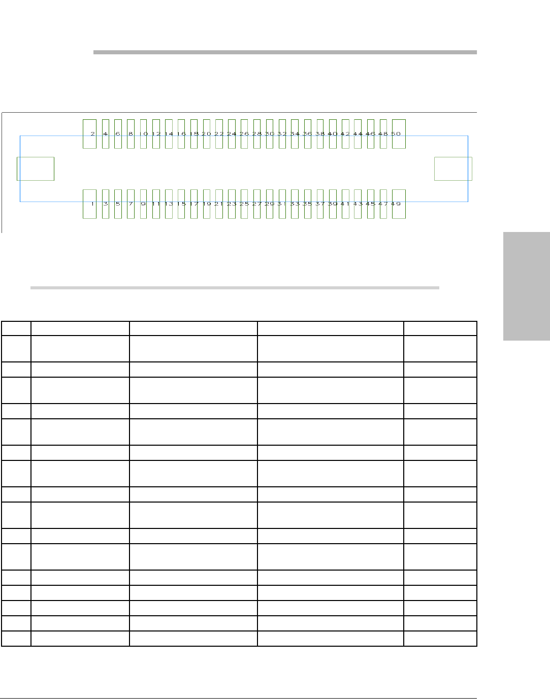
50-pin Module interface connector pin assignments (viewed looking down on connector)
=páÖå~ä=ÇÉÑáåáíáçåë=çÑ=RMJéáå=jçÇìäÉ=áåíÉêÑ~ÅÉ=ÅçååÉÅíçê
EfåéìíLçìíéìí=~êÉ=áå=êÉÑÉêÉåÅÉ=íç=jçÇìäÉKF
Pin # Signal Name Comment Modem Signal Level Type
1 VPH_PWR Power to the CDMA
transceiver
3.6 VDC min to 4.2 VDC max Power input(6)
2 GND Signal and power return GROUND
3 VPH_PWR Power to the CDMA
transceiver
3.6 VDC min to 4.2 VDC max Power input(6)
4 GND Signal and power return GROUND
5 VPH_PWR Power to the CDMA
transceiver
3.6 VDC min to 4.2 VDC max Power input(6)
6 GND Signal and power return GROUND
7 VPH_PWR Power to the CDMA
transceiver
3.6 VDC min to 4.2 VDC max Power input(6)
8 GND Signal and power return GROUND
9 VPH_PWR Power to the CDMA
transceiver
3.6 VDC min to 4.2 VDC max Power input(6)
10 GND Signal and power return GROUND
11 VEXT# Indicates that external
power is being used
0 to VPH_PWR max Analog control
12 N/C No connection
13 N/C No connection
14 LED_EN# Enable external LED 0 to VPH_PWR max Analog control
15 N/C No connection
16 LED_DRV External LED drive 10 mA LED drive Analog output
82 Kyocera 200 Module Data Book Kyocera Proprietary
^ëëáÖåãÉåíë=~åÇ=páÖå~ä=aÉÑáåáíáçåë UOJjUUSOJN=oÉîK=MMP
17 N/C No connection
18 XCVR_DET Indicates that transceiver
is on
Digital output(2)
19 N/C No connection
20 N/C No connection
21 XCVR_EN# CDMA transceiver primary
power enable
0 to VPH_PWR max Analog input
22 MSM_DP_TXD UART1 - transmit data VOH(min) = 2.4V,
VOL(max) = 0.5V
Digital output(1)
23 MSM_DP_RXD UART1 - receive data VIH(min) = 1.9V,
VIL(max) = 0.9V
Digital input(2)
24 MSM_DP_CTS# UART1 - clear to send VIH(min) = 1.9V,
VIL(max) = 0.9V
Digital input(2)
25 MSM_DP_RTS# UART1 - ready for receive VOH(min) = 2.4V,
VOL(max) = 0.5V
Digital output(1)
26 MSM_DP_DTR# UART1 - data terminal
ready
VIH(min) = 1.9V,
VIL(max) = 0.9V
Digital
input(2,3)
27 MSM_DP_RI# UART1 - ring indicator VOH(min) = 2.4V,
VOL(max) = 0.5V
Digital output(1)
28 MSM_DP_DCD# UART1 - data carrier detect VOH(min) = 2.4V,
VOL(max) = 0.5V
Digital output(1)
29 HS_PRES# Headset detection input to
MSM
VIH(min) = 1.9V,
VIL(max) = 0.9V
Digital
input(2,3)
30 GND Signal and power return GROUND
31 MSM_DP_TXD2 UART2 - transmit data VOH(min) = 2.4V,
VOL(max) = 0.5V
Digital output(1)
32 MSM_DP_RXD2 UART2 - receive data VIH(min) = 1.9V,
VIL(max) = 0.9V
Digital input(2)
33 MSM_DP_CTS2# UART2 - clear to send VIH(min) = 1.9V,
VIL(max) = 0.9V
Digital input(2)
34 MSM_DP_RTS2# UART2 - ready for receive VOH(min) = 2.4V,
VOL(max) = 0.5V
Digital output(1)
35 GND Signal and power return GROUND
36 CAR_SCL Analog Carkit SCL line VOH(min) = 2.4V,
VOL(max) = 0.5V
Input/output
37 CAR_SDA Analog Carkit SDA line VOH(min) = 2.4V,
VOL(max) = 0.5V
Input/output(1)
38 CAR_MIC+ Analog carkit microphone
input
VIH(min) = 1.9V,
VIL(max) = 0.9V
Analog input(2)
39 CAR_SPKR+ Analog Carkit Speaker
output
VOH(min) = 2.4V,
VOL(max) = 0.5V
Analog
output(1)
40 GND Signal and power return GROUND
=páÖå~ä=ÇÉÑáåáíáçåë=çÑ=RMJéáå=jçÇìäÉ=áåíÉêÑ~ÅÉ=ÅçååÉÅíçê
EfåéìíLçìíéìí=~êÉ=áå=êÉÑÉêÉåÅÉ=íç=jçÇìäÉKF
Pin # Signal Name Comment Modem Signal Level Type
Assignments and Signal
Definitions
Assignments and Signal
Definitions
Assignments and Signal
Definitions
Assignments and Signal
Definitions
Assignments and Signal
Definitions
Kyocera Proprietary Kyocera 200 Module Data Book 83
UOJjUUSOJN=oÉîK=MMP ^ëëáÖåãÉåíë=~åÇ=páÖå~ä=aÉÑáåáíáçåë
41 HS_SPEAKER Headset speaker audio
output
1.5Vpp, 8.8mW into 32 ohm
load
Analog
output(1)
42 GND Signal and power return GROUND
43 MAIN_MIC+ Main microphone positive
input
1.8VDC nominal, -3Mv rms Electret
microphone
input(4)
44 MAIN_MIC- Handset microphone
negative terminal
GROUND
45 GND Signal and power return GROUND
46 EAR_SPKR+ Main speaker positive
audio output
1.2VDC nominal,
3V pp with pin 47
Bridge amp
output(5)
47 EAR_SPKR- Main speaker negative
audio terminal
1.2VDC nominal,
3V pp with pin 46
48 HS_MIC+ Headset microphone input 1.8VDC nominal, ~3Mv rms Electret
microphone
input(4)
49 GND Ground for headset
microphone
GROUND
50 LSPKR_ON Loudspeaker amp control
output
VOH(min) = 2.4V,
VOL(max) = 0.5V
Digital output(2)
Notes:
1. Input connected directly to MSM. Do not exceed V(max) of 3.1V; damage to MSM may result.
2. Output connected directly to MSM. Do not exceed V(max) of 2.8V; damage to MSM may result.
3. 10K ohm pull-up resistor inside Module.
4. Input for standard electret microphone. 1.8V supplied via 2.2K ohm resistor inside Module.
5. Pins 46 and 47 are bridge (differential) amp outputs capable of driving 35 mW into a 32 ohm speaker
connected between these pins.
6. 1200 mA required for full analog transmission capabilities.
=páÖå~ä=ÇÉÑáåáíáçåë=çÑ=RMJéáå=jçÇìäÉ=áåíÉêÑ~ÅÉ=ÅçååÉÅíçê
EfåéìíLçìíéìí=~êÉ=áå=êÉÑÉêÉåÅÉ=íç=jçÇìäÉKF
Pin # Signal Name Comment Modem Signal Level Type

84 Kyocera 200 Module Data Book Kyocera Proprietary
^ëëáÖåãÉåíë=~åÇ=páÖå~ä=aÉÑáåáíáçåë UOJjUUSOJN=oÉîK=MMP

Module Developer’s Kit
Schematic
Module Developer’s Kit
Schematic
Module Developer’s Kit
Schematic
Module Developer’s Kit
Schematic
Module Developer’s Kit
Schematic
Kyocera Proprietary Kyocera 200 Module Data Book 85
NS
jçÇìäÉ=aÉîÉäçéÉêÛë=háí=pÅÜÉã~íáÅ
There are two earlier versions of the Module Developer’s Kit (MDK) interface
board.
If the interface board in your MDK has an identifier of either K4020 or K4021,
you may request a schematic diagram by emailing
module-support@kyocera-wireless.com.

86 Kyocera 200 Module Data Book Kyocera Proprietary
jçÇìäÉ=aÉîÉäçéÉêÛë=háí=pÅÜÉã~íáÅ UOJjUUSOJN=oÉîK=MMP