LANKE XUNTONG TECHNOLOGY PTR5618PA Bletooth low energy 4.0 modules User Manual
LANKE XUNTONG TECHNOLOGY CO.,LTD Bletooth low energy 4.0 modules Users Manual
UserManual.wiki
>
LANKE XUNTONG TECHNOLOGY
>
PTR5618PA User Manual
>
User Manual
Contents
1.
User Manual
2.
User manual
User Manual
Navigation menu
Upload a User Manual
Namespaces
Wiki Guide
HTML
PDF
Info
Views
User Manual
Discussion / Help
Navigation
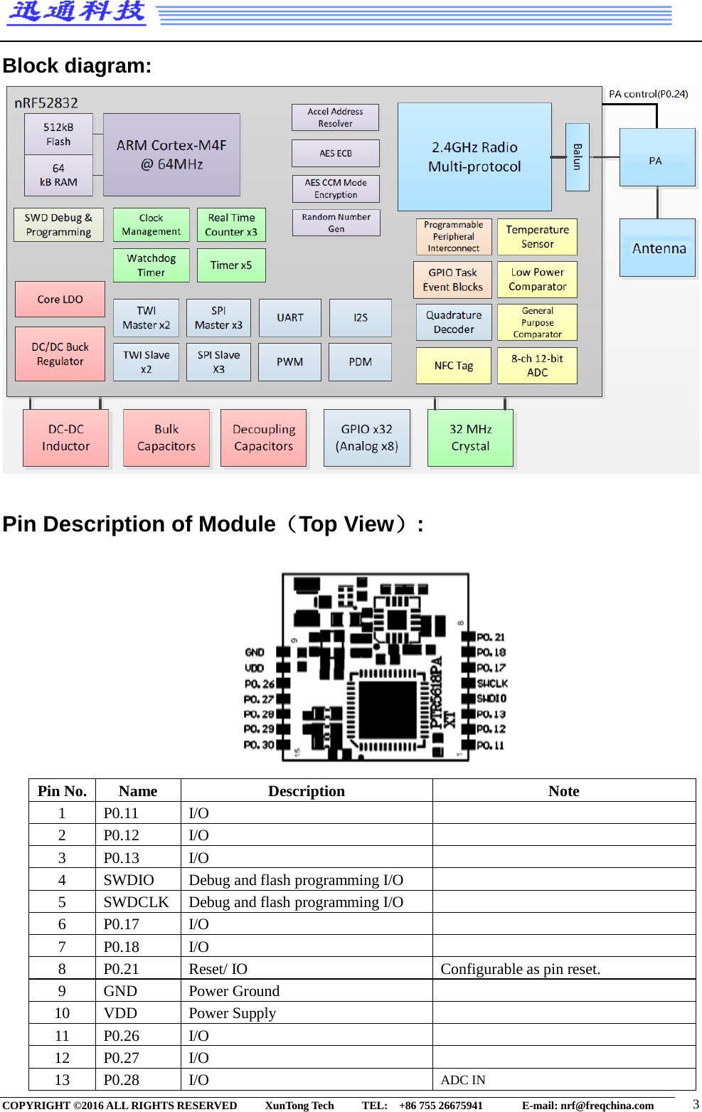
![Hardware RESET: There is on-chip power-on reset circuitry, But can still be used in external reset mode, in this case, GPIO pin P0.21 as an external hardware reset pin(Active Low). In order to utilize P0.21 as a hardware reset, the UICR registers PSELRESET[0] and PSELRESET[1] must be set alike, to the value of 0x7FFFFF15. When P0.21 is programmed as RESET, the internal pull-up is automatically enabled. HW debug and flash programming of Module: The Module support the two pin Serial Wire Debug (SWD) interface and offers flexible and powerful mechanism for non-intrusive debugging of program code. Breakpoints, single stepping, and instruction trace capture of code execution flow are part of this support. Pin Flash Program interface SWDIO Debug and flash programming I/O SWCLK Debug and flash programming I/O This is the hardware debug and flash programming of module, J-Link Lite support, please refer www.segger.com. COPYRIGHT ©2016 ALL RIGHTS RESERVED XunTong Tech TEL: +86 755 26675941 E-mail: nrf@freqchina.com 7](https://usermanual.wiki/LANKE-XUNTONG-TECHNOLOGY/PTR5618PA.User-Manual/User-Guide-3214483-Page-7.png)