LANKE XUNTONG TECHNOLOGY PTR5618PA Bletooth low energy 4.0 modules User Manual
LANKE XUNTONG TECHNOLOGY CO.,LTD Bletooth low energy 4.0 modules Users Manual
Contents
- 1. User Manual
- 2. User manual
User Manual

Coin-size Bluetooth Low Energy System on Module with PA
Embedded Cortex™ M4F 32 bit processor
The PTR5618PA ultra-low power Bluetooth Low Energy/2.4GHz Proprietary Multi-protocol
modules based on the nRF52832 from Nordic Semiconductor. The module with an ARM®
Cortex™ M4F 32 bit processor, embedded 2.4GHz transceiver, and integrated antenna,
provide a complete solution with no additional RF design, allowing faster time to market,
while simplifying designs, reducing BOM costs, also reduce the burden of Regulatory
approvals to enter the world market. Making you more quickly into the bluetooth smart
application and remove the worries.
Features
System on Module(SOM) base on Nordic nRF52832
Bluetooth Low Energy/2.4GHz Proprietary Multi-protocol support
Complete Bluetooth Low Energy stack/profiles solution (Bluetooth 4.x and Higher)
ARM® Cortex™-M4F 32 bit processor, 512 kB flash memory, 64 kB RAM
2.4 GHz transceiver, Max TX Power +15 dBm, -96 dBm sensitivity@BLE
11 General Purpose I/O, Configurable mapping Pins, Simple layout of external application
12-bit/200KSPS ADC, PWM, SPI Master/Slave (8 Mbps)
Low power comparator, Temperature sensor, Random Number Generator
Two 2-wire Master/Slave (I2C compatible)
I2S audio interface, PDM audio interface
UART (w/ CTS/RTS and DMA)
20 channel CPU independent Programmable Peripheral Interconnect (PPI)
Quadrature Demodulator (QDEC)
128-bit AES HW encryption
5 x 32bit Timers, 3 x 24bit Real Timer Counters (RTC), Watchdog Timer
Internal RC Oscillator 32.768 kHz(± 250 ppm).
No external components required
Over-the-Air (OTA) firmware updates available
Ultra small size(smaller than CR2032 coin battery), about 15mmx15mmx1.8mm.
PTR5618PA
COPYRIGHT ©2016 ALL RIGHTS RESERVED XunTong Tech TEL: +86 755 26675941 E-mail: nrf@freqchina.com
1
Typical Applications:
- 2.4 GHz Bluetooth low energy systems
- Proprietary 2.4 GHz systems
- Sports and leisure equipment
- Mobile phone accessories
- Health Care and Medical
- Consumer Electronics, Game pads
- Human Interface Devices, Remote control
- Building environment control / monitoring
- RFID, Security Applications
- Bluetooth Low Energy GateWay
- iBeacons™, Eddystone™, Indoor navigation
- Low-Power Sensors
- Connected Appliances
- Lighting Products
- Fitness devices
- Wearables
Quick Specifications:
Multi-protocol
Version Bluetooth 4.x and Higher/ANT/2.4GHz Proprietary
Security AES-128
Radio
Frequency 2.402GHz to 2.480GHz
Modulations
GFSK at 1 Mbps, 2 Mbps data rates
Transmit power
Max +15dBm @setting nRF52832 0dBm output
Receiver sensitivity
-96dBm (BLE mode)
Antenna IPX interface
Current Consumption
TX only @ +15 dBm ~100 mA
RX only @ 1 Mbps @ 3V, DC/DC enabled ~5.4 mA
RX only @ 1 Mbps ~11.7 mA
CPU @ 64MHz from flash 7.5 mA
CPU @ 64MHz from RAM
6.7 mA
CPU @ 64MHz from flash @ 3V, DC/DC
3.7 mA
CPU @ 64MHz from flash RAM @ 3V, DC/DC
3.3 mA
System On
1.2 μA
System Off 0.7μA
Operating conditions
Power supply 2.7~3.6V
Operating temperature -25~+85 °C
COPYRIGHT ©2016 ALL RIGHTS RESERVED XunTong Tech TEL: +86 755 26675941 E-mail: nrf@freqchina.com
2
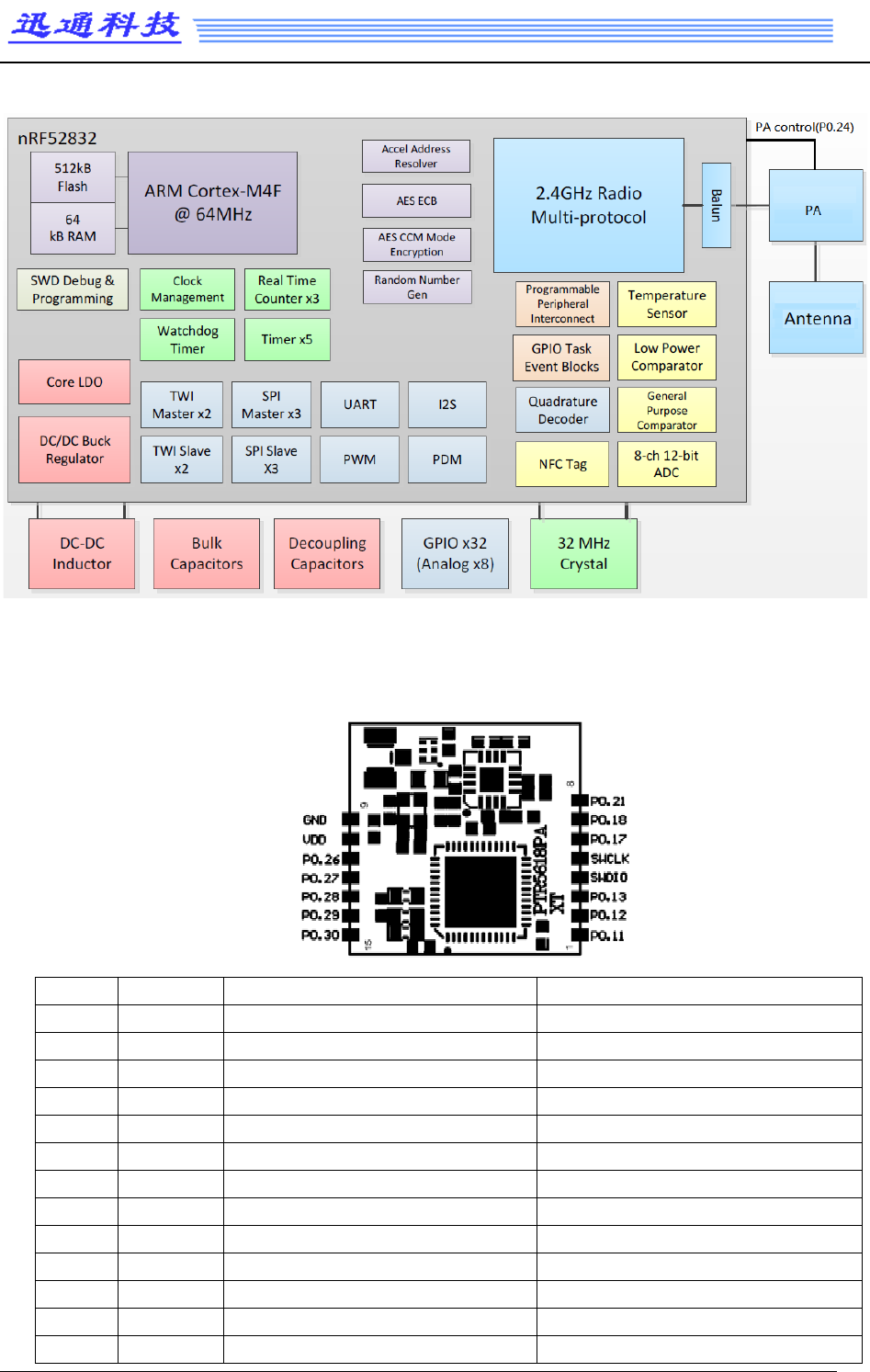
Block diagram:
Pin Description of Module
(
Top View
)
:
Pin No.
Name
Description
Note
1
P0.11
I/O
2
P0.12
I/O
3
P0.13
I/O
4
SWDIO
Debug and flash programming I/O
5
SWDCLK
Debug and flash programming I/O
6
P0.17
I/O
7
P0.18
I/O
8
P0.21
Reset/ IO
Configurable as pin reset.
9
GND
Power Ground
10
VDD
Power Supply
11
P0.26
I/O
12
P0.27
I/O
13
P0.28
I/O
ADC IN
COPYRIGHT ©2016 ALL RIGHTS RESERVED XunTong Tech TEL: +86 755 26675941 E-mail: nrf@freqchina.com
3
14
P0.29
I/O
ADC IN
15
P0.30
I/O
ADC IN
Note 1: P0.20 and P0.24 are reserved for PA control internal.
Note 2: An internal 4.7μF bulk capacitor has been included on the module. it is good design
practice to add additional bulk capacitance(e.g 10uF) as required for your application.
General Purpose I/O:
The general purpose I/O is organized as one port enabling access and control of the 32 available
GPIO pins through one port. Each GPIO can be accessed individually with the following user
configurable features:
Input/output direction
Output drive strength
Internal pull-up and pull-down resistors
Wake-up from high or low level triggers on all pins
Trigger interrupt on all pins
All pins can be used by the PPI task/event system; the maximum number of pins that can be
interfaced through the PPI at the same time is limited by the number of GPIOTE channels
All pins can be individually configured to carry serial interface or quadrature demodulator
signals
PA control:
Additional logic signals are needed to control TX PA and RX LNA. On the nRF51 there was an
option to use the VDD_PA pin to detect when the radio was in TX mode, but this is not an option on
the nRF52, making the SoftDevice solution necessary. The S132 SoftDevice for the nRF52 has
support for enable/disable switching of external Power Amplifiers (PA) and LNA using GPIO pins.
On the module, P0.20 and P0.24 are reserved to control PA and LNA, so these two pins can Not
be allocated to other usage.
The truth table of PA/LNA control signals as bellow:
PIN24 PIN20 PA status
1 0 TXEN
0 1 RXEN
0 0 IDLE
1 1 INVALID
The following function can be used to enable PA/LNA signal with P0.20 and P0.24. Add this
function to your project and call it after ble_stack_init():
static void pa_assist(uint32_t gpio_pa_pin,uint32_t gpio_lna_pin)
{
ret_code_t err_code;
COPYRIGHT ©2016 ALL RIGHTS RESERVED XunTong Tech TEL: +86 755 26675941 E-mail: nrf@freqchina.com
4

static const uint32_t gpio_toggle_ch = 0;
static const uint32_t ppi_set_ch = 0;
static const uint32_t ppi_clr_ch = 1;
// Configure SoftDevice PA assist
ble_opt_t opt;
memset(&opt, 0, sizeof(ble_opt_t));
// Common PA config
opt.common_opt.pa_lna.gpiote_ch_id = gpio_toggle_ch; // GPIOTE channel
opt.common_opt.pa_lna.ppi_ch_id_clr = ppi_set_ch; // PPI channel for pin clearing
opt.common_opt.pa_lna.ppi_ch_id_set = ppi_clr_ch; // PPI channel for pin setting
// PA config
opt.common_opt.pa_lna.pa_cfg.active_high = 1; // Set the pin to be active high
opt.common_opt.pa_lna.pa_cfg.enable = 1; // Enable toggling
opt.common_opt.pa_lna.pa_cfg.gpio_pin = gpio_pa_pin; // The GPIO pin to toggle
opt.common_opt.pa_lna.lna_cfg.active_high = 1;
opt.common_opt.pa_lna.lna_cfg.enable = 1;
opt.common_opt.pa_lna.lna_cfg.gpio_pin = gpio_lna_pin;
err_code = sd_ble_opt_set(BLE_COMMON_OPT_PA_LNA, &opt);
APP_ERROR_CHECK(err_code);
}
COPYRIGHT ©2016 ALL RIGHTS RESERVED XunTong Tech TEL: +86 755 26675941 E-mail: nrf@freqchina.com
5

The following main function is an example that to show you how to enable PA/LNA signal in your
project:
int main(void)
{
uint32_t err_code;
// Initialize.
APP_TIMER_INIT(APP_TIMER_PRESCALER, APP_TIMER_OP_QUEUE_SIZE, false);
ble_stack_init();
pa_assist(24,20);
gap_params_init();
services_init();
advertising_init();
conn_params_init();
err_code = ble_advertising_start(BLE_ADV_MODE_FAST);
APP_ERROR_CHECK(err_code);
// Enter main loop.
for (;;)
{
power_manage();
}
}
COPYRIGHT ©2016 ALL RIGHTS RESERVED XunTong Tech TEL: +86 755 26675941 E-mail: nrf@freqchina.com
6

Hardware RESET:
There is on-chip power-on reset circuitry, But can still be used in external reset mode, in this case,
GPIO pin P0.21 as an external hardware reset pin(Active Low). In order to utilize P0.21 as a hardware
reset, the UICR registers PSELRESET[0] and PSELRESET[1] must be set alike, to the value of
0x7FFFFF15. When P0.21 is programmed as RESET, the internal pull-up is automatically enabled.
HW debug and flash programming of Module:
The Module support the two pin Serial Wire Debug (SWD) interface and offers flexible and powerful
mechanism for non-intrusive debugging of program code. Breakpoints, single stepping, and
instruction trace capture of code execution flow are part of this support.
Pin Flash Program interface
SWDIO Debug and flash programming I/O
SWCLK Debug and flash programming I/O
This is the hardware debug and flash programming of module, J-Link Lite support, please refer
www.segger.com.
COPYRIGHT ©2016 ALL RIGHTS RESERVED XunTong Tech TEL: +86 755 26675941 E-mail: nrf@freqchina.com
7
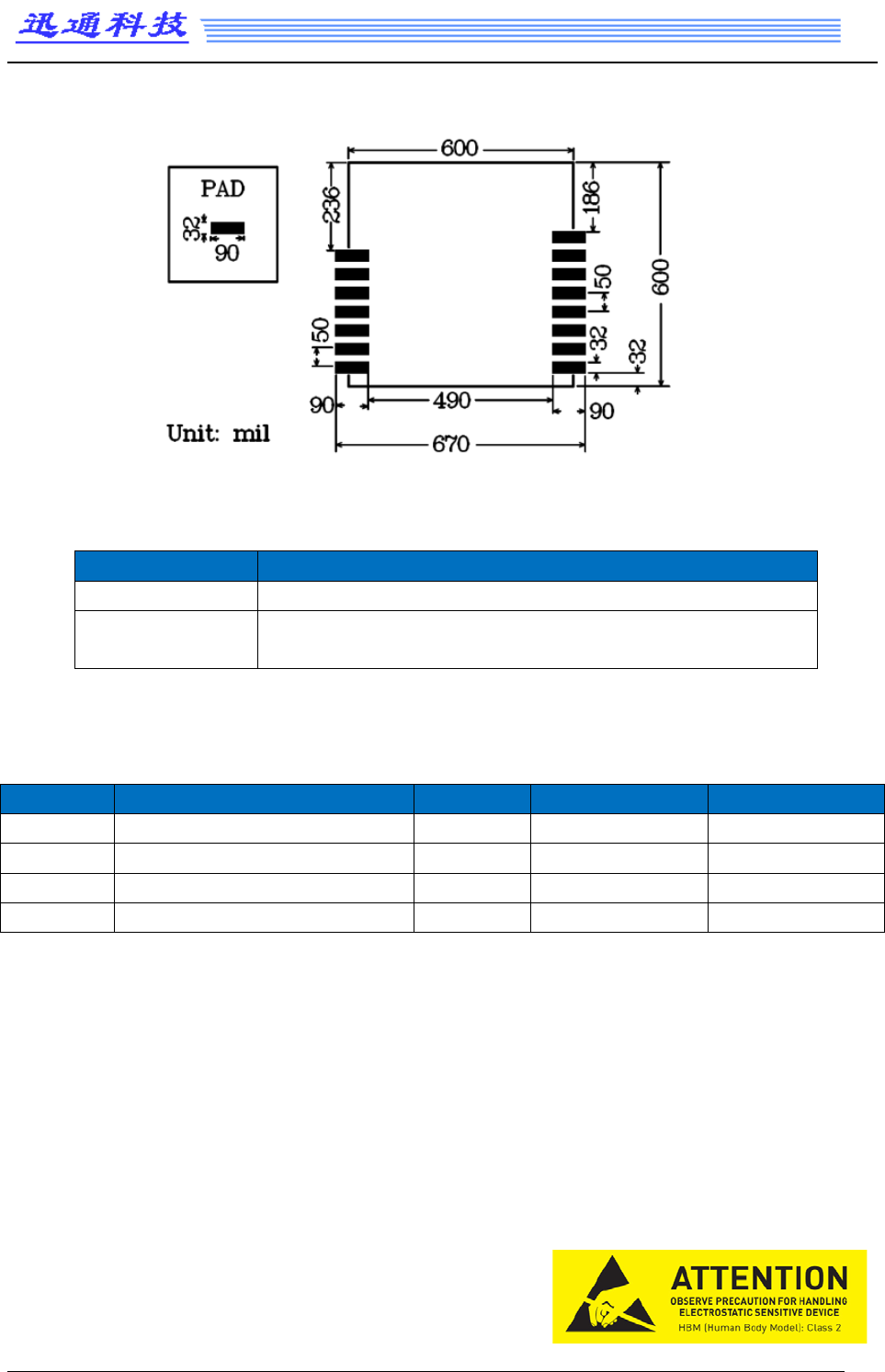
PCB Footprint
(
Top View
)
:
Ordering Information:
Part Number
Description
PTR5618PA
Bluetooth Low Energy System on Module with PA
PTR5618PA-EVB Evaluation boards for module,with key, LED, I/O extend,sock
for coin cell battery.
Absolute Maximum Ratings:
Symbol
Parameter
Min.
Max.
Unit
V
CC_MAX
Voltage on supply pin
-0.3
3.9
V
V
IO_MAX
Voltage on GPIO pins (V
CC
> 3.6V)
-0.3
3.9
V
V
IO_MAX
Voltage on GPIO pins (V
CC
≤ 3.6V)
-0.3
V
CC
+ 0.3V
V
TS Storage Temperature Range -40 125 °C
Important Notice:
Reserves the right to make corrections, modifications, and/or improvements to the product and/or
its specifications at any time without notice.
Assumes no liability for the user’s product and/or applications.
Products are not authorized for use in safety-critical applications, including but not limited to
life-support applications.
ATTENTION!
Electrostatic Sensitive Device
Observe Precaution for handling.
COPYRIGHT ©2016 ALL RIGHTS RESERVED XunTong Tech TEL: +86 755 26675941 E-mail: nrf@freqchina.com
8