LG Electronics USA LEO3-BAND13 LTE User Equipment User Manual
LG Electronics USA LTE User Equipment Users Manual
UserManual.wiki
>
LG Electronics USA
>
LEO3 BAND13 User Manual
Users Manual
Navigation menu
Upload a User Manual
Namespaces
Wiki Guide
HTML
PDF
Info
Views
User Manual
Discussion / Help
Navigation
![Updated File BAND13 RF board manual Rev. LGE Proprietary ii MCTR Lab. 1 2 3 4 5 6 7 8 9 10 11 12 13 14 15 16 17 18 19 20 21 22 23 24 25 26 27 28 29 30 31 32 33 34 35 36 37 38 39 40 41 42 43 [Notice] 44 1. The product described in this manual may be modified without prior notice for reliability, 45 functionality or design improvement. 46 2. Information contained in this manual is correct and reliable, but LG shall not be held 47 responsible for damage due to the use of information, product or circuit or infringement of 48 property rights or other rights. 49 3. This manual does not grant users the property rights and other rights of the third party or LG 50 Electronics Inc. 51 4. No part of this manual may be transcribed or duplicated without the written permission of LG 52 Electronics Inc. 53 5. The appearance of the product shown in this manual may slightly differ from that of the actual 54 product. 55](https://usermanual.wiki/LG-Electronics-USA/LEO3-BAND13/User-Guide-1114075-Page-3.png)
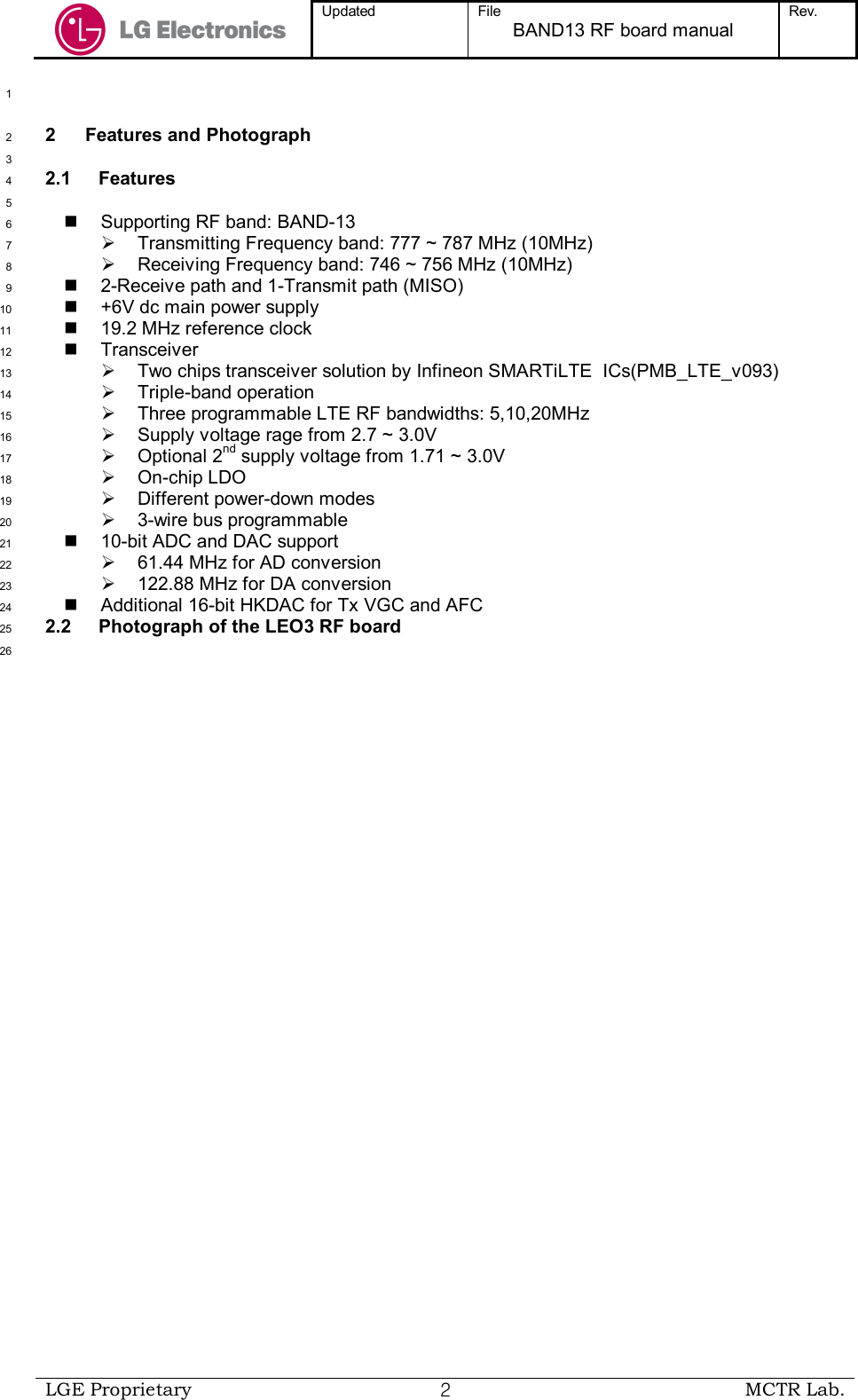
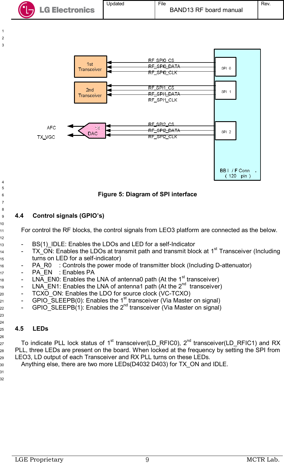
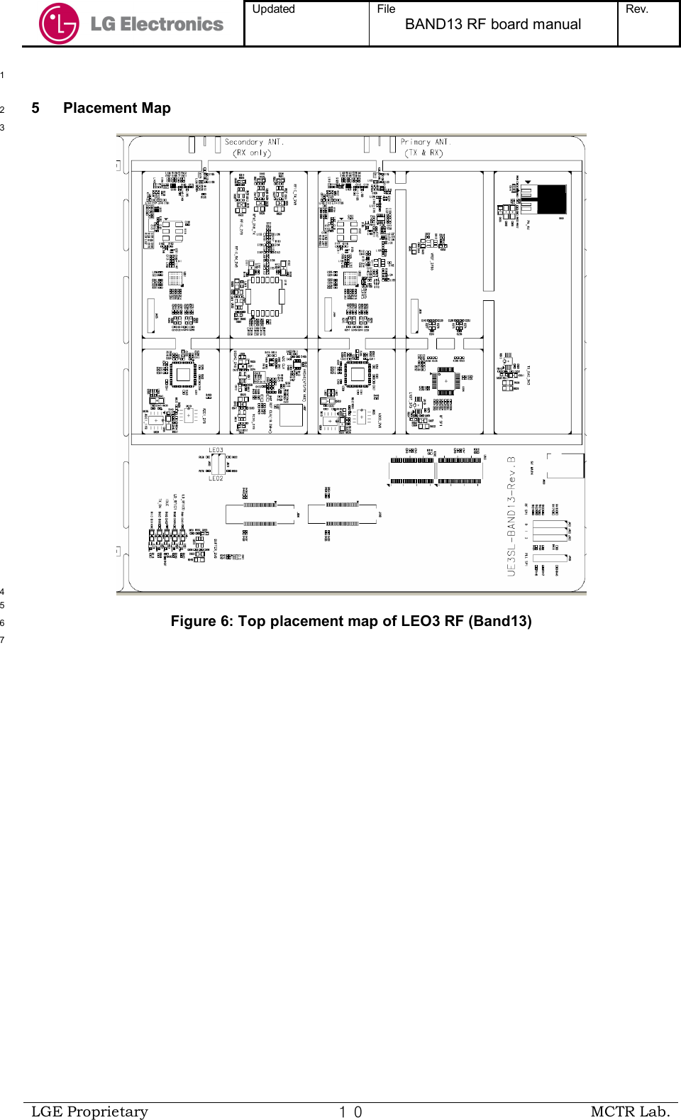
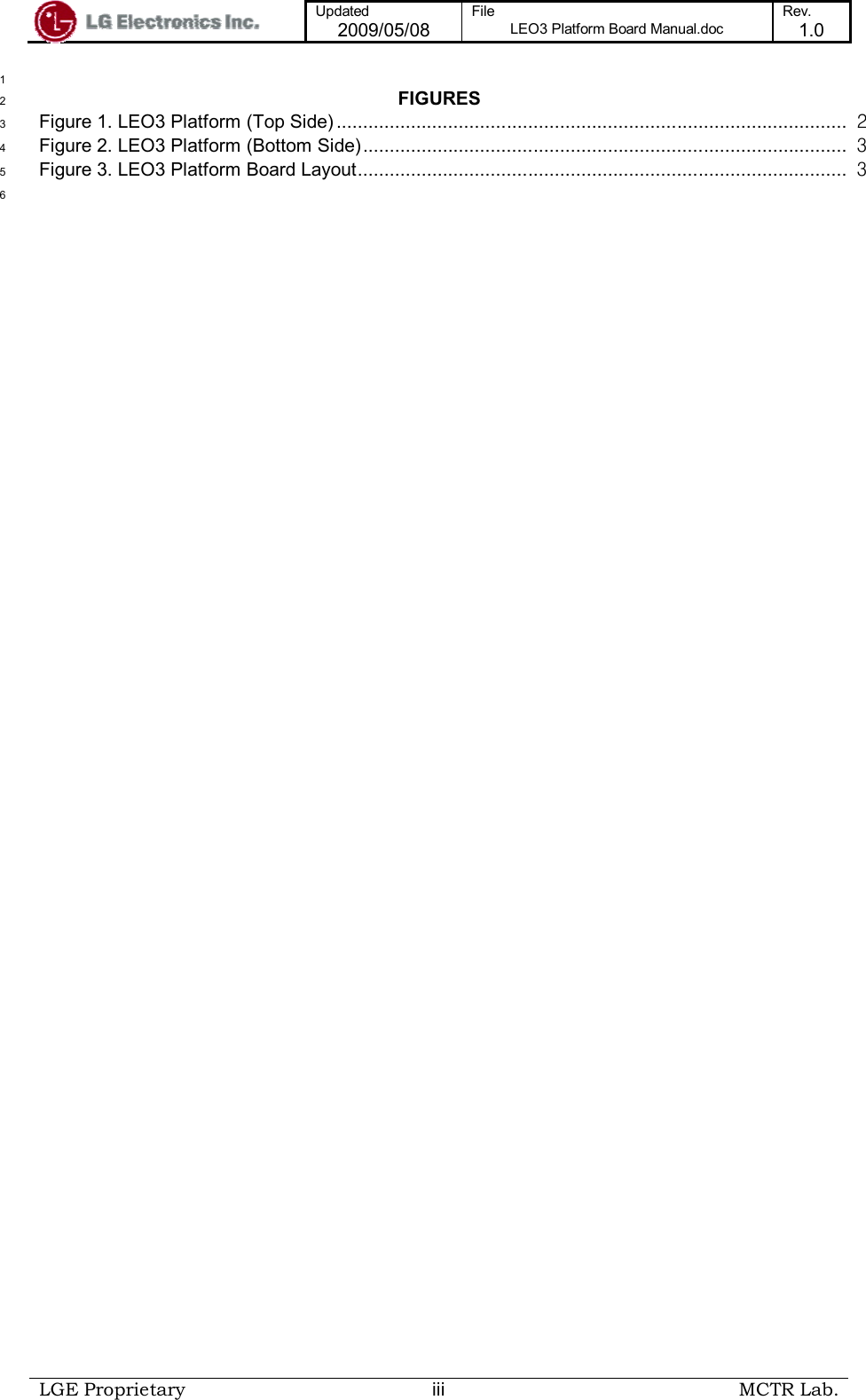
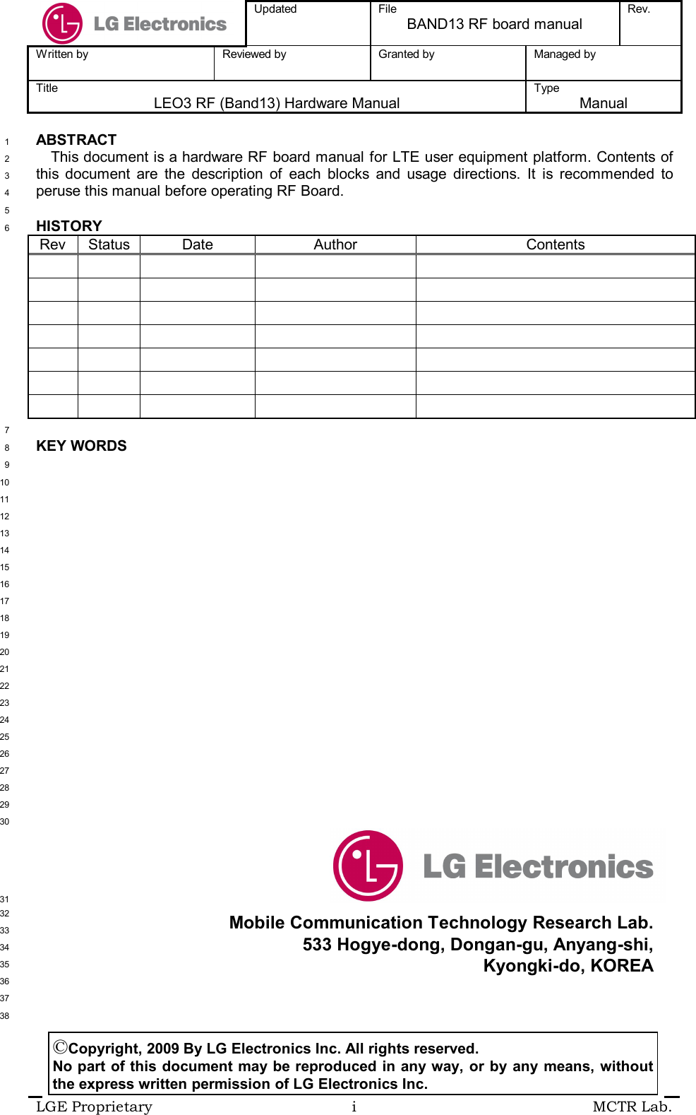
![Updated 2009/05/08 File LEO3 Platform Board Manual.doc Rev. 1.0 LGE Proprietary 5 MCTR Lab. 1 SW7 No. Name Default Description 1 JTAG_CFG(0) ON 2 JTAG_CFG(1) OFF JTAG_CFG[1:0] [OFF:OFF] No JTAG [OFF:ON] ARM Only [ON:OFF] CC5 Only [ON:ON] ARM-CC5 *ON: High, OFF: Low 3 EPI_MODE ON [OFF] Dedicated Address/Data EPI I/O [ON] Muxed Address/Data EPI I/O *ON: HIgh, OFF: Low 4 USB_MODE OFF [OFF] UTMI mode [ON] ULPI mode *ON: High OFF: Low 5 PWR_CUT_MODE OFF [OFF] Power cut disable [ON] Power cut enable *ON: High, OFF: Low 6 REFCLK_SEL OFF [OFF] On-board VCTCXO 19.2MHz [ON] RF board 19.2MHz *ON: High, OFF: Low (Rev.A) *ON: Low, OFF: High (Rev.B) 7 NAND_CFG(0) OFF [ON] 4byte address [OFF] 5byte address *ON: Low, OFF: High 8 NAND_CFG(1) OFF [ON] Small block (1page: 512byte + 16byte) [OFF] Large block (1page 2048byte +64byte) *ON: Low, OFF: High SW8 No. Name Default Description 1 MODE(0) ON 2 MODE(1) OFF 3 MDOE(2) OFF MODE[2:0] [OFF:OFF:OFF] Undefined [OFF:OFF:ON] NAND boot [OFF:ON:OFF] Serial Flash boot [OFF:ON:ON] EPI boot [ON:OFF:OFF] SDIO boot [ON:OFF:ON] USB boot [ON:ON:OFF] Serial Flash boot (for debug) [ON:ON:ON] Test *ON: High, OFF: Low 4 MODE(3) OFF [OFF] Secure Boot disable [ON] Secure Boot enable *ON: High OFF: Low Table 1. DIP switch setting for L1000 boot configuration 2 3 4](https://usermanual.wiki/LG-Electronics-USA/LEO3-BAND13/User-Guide-1114075-Page-25.png)
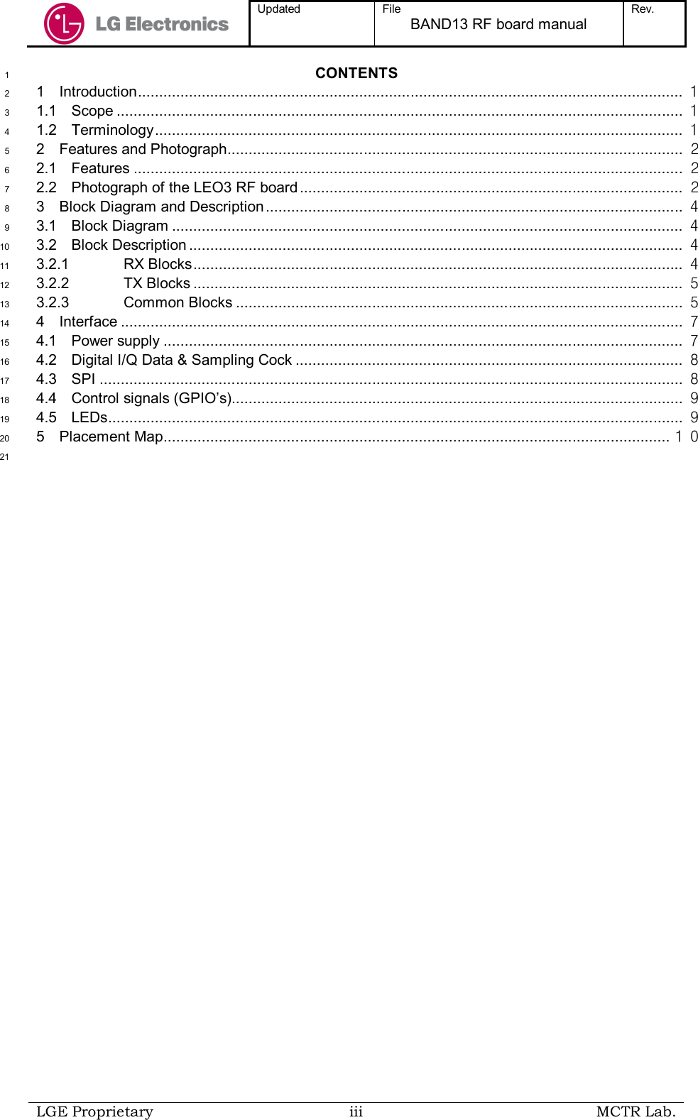
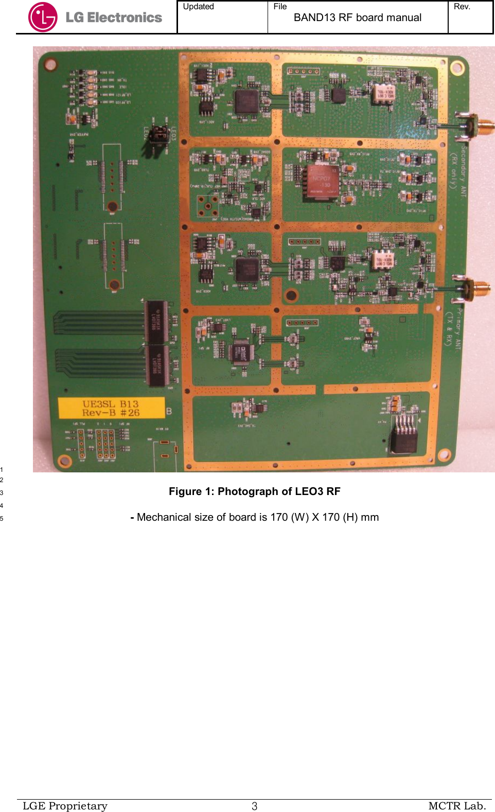
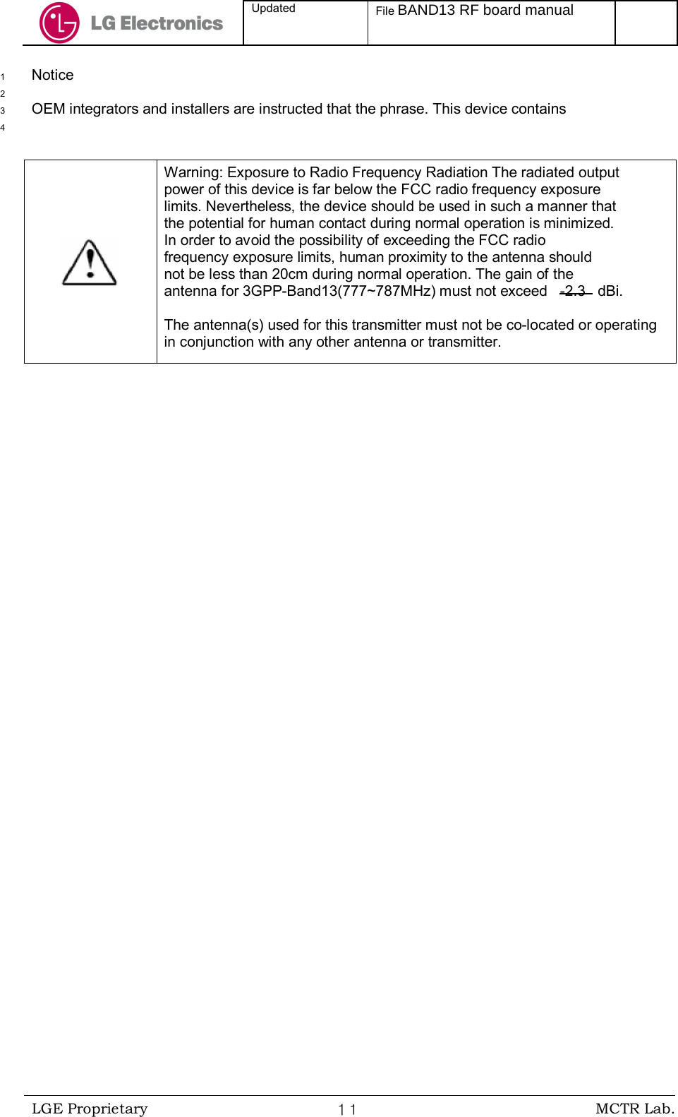
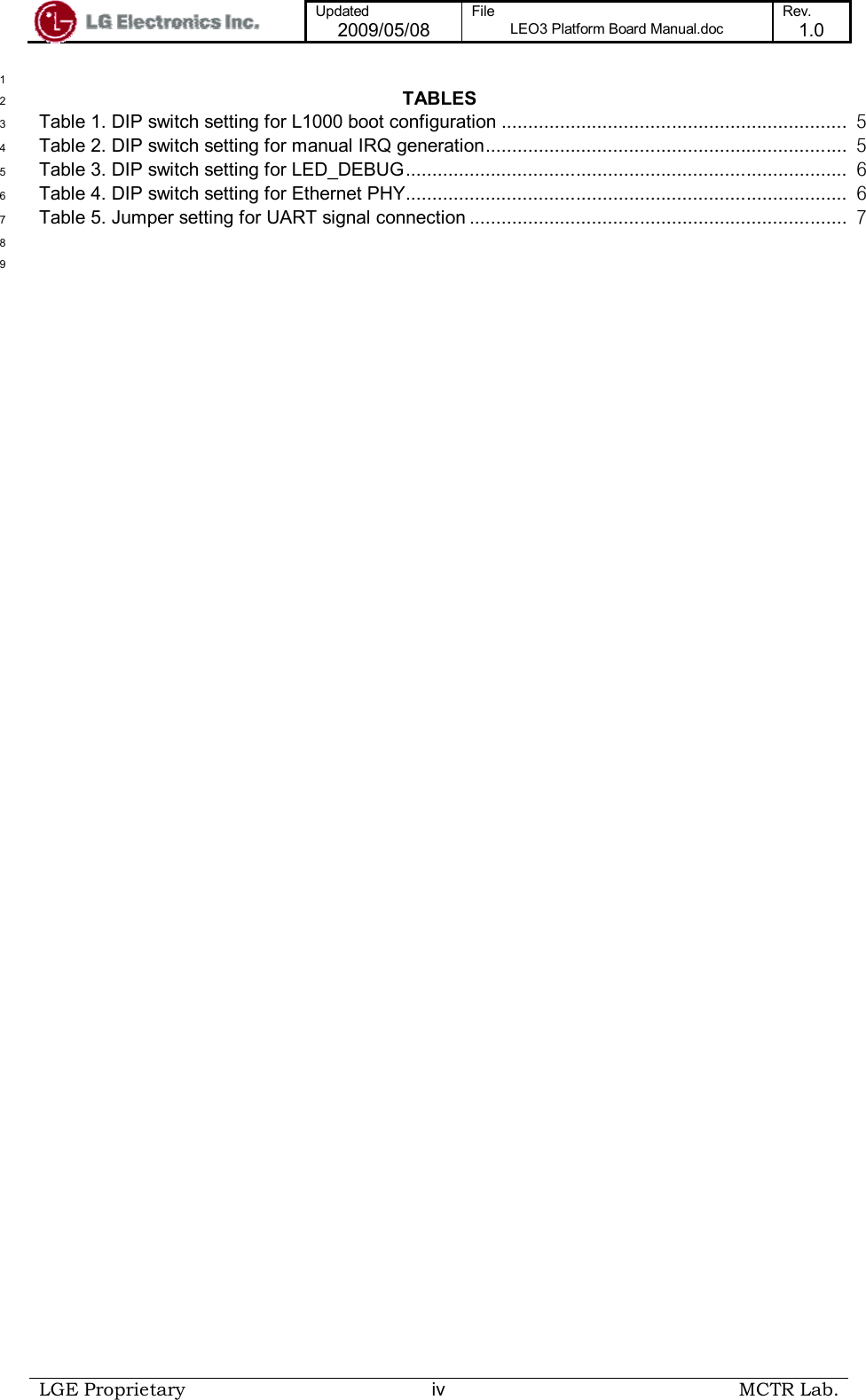
![Updated 2009/05/08 File LEO3 Platform Board Manual.doc Rev. 1.0 LGE Proprietary 6 MCTR Lab. SW6 No. Name Default Description 1 IRQ(0) OFF [OFF] Low level [ON] High level *ON: High, OFF: Low 2 IRQ(1) OFF [OFF] High level (Rev.A), Low level (Rev.B) [ON] Low level (Rev.A), High level (Rev.B) *ON: High, OFF: Low (Rev.A) *ON: Low, OFF: High (Rev.B) 3 IRQ(2) OFF [OFF] High level [ON] Low level *ON: Low, OFF: High 4 IRQ(3) OFF [OFF] High level [ON] Low level *ON: Low, OFF: High Table 2. DIP switch setting for manual IRQ generation 1 2](https://usermanual.wiki/LG-Electronics-USA/LEO3-BAND13/User-Guide-1114075-Page-26.png)
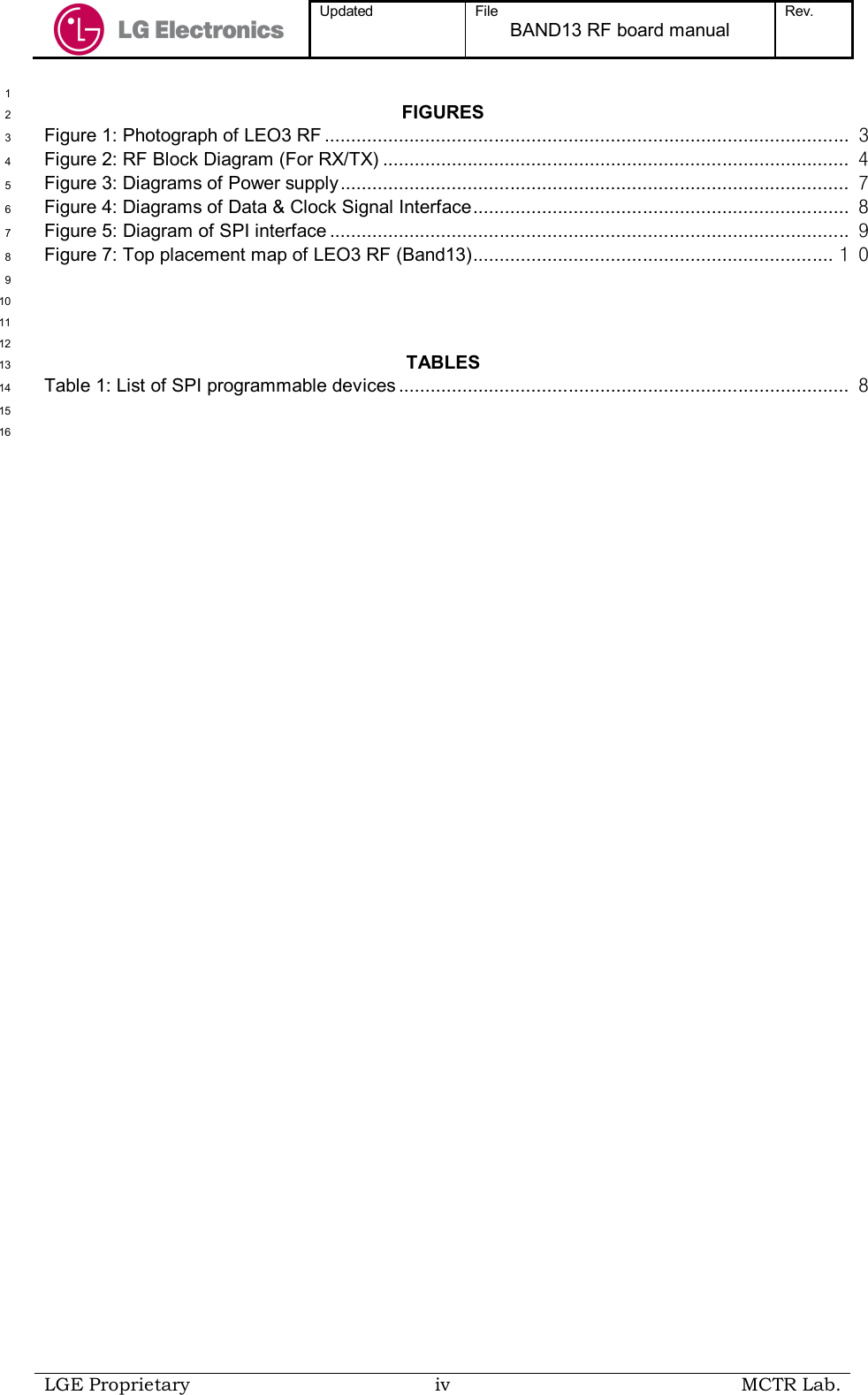
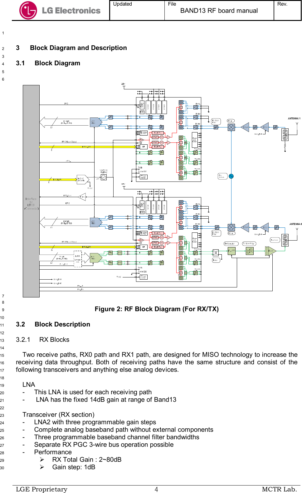
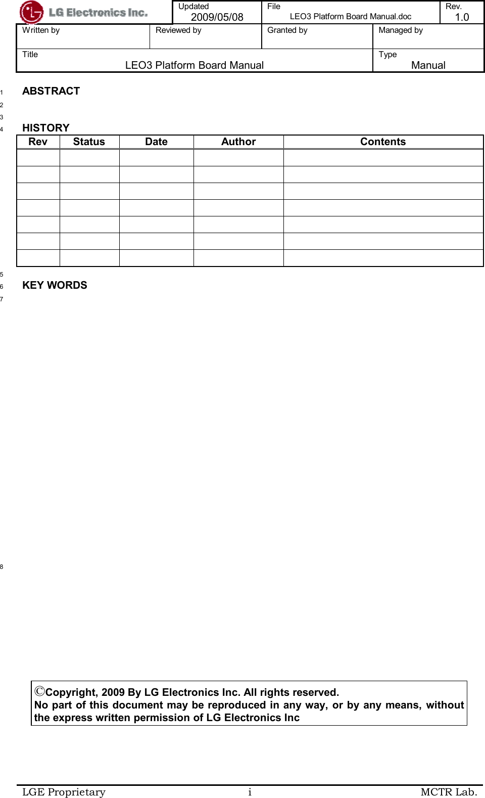
![Updated 2009/05/08 File LEO3 Platform Board Manual.doc Rev. 1.0 LGE Proprietary 7 MCTR Lab. 1 * Caution) Please, be careful to switch ‘ON” for the SW5. Switching ‘ON’ should be done 2 only when the corresponding GPIO directions have defined as ‘Input’. Otherwise (if 3 defined as ‘Output’), it would be possible for the L1000 to have a damage. 4 SW5 No. Name Default Description 1 LED_DEBUG(0) OFF Corresponding to GPIO(0) of L1000 [OFF] Low level [ON] High level *ON: High, OFF: Low 2 LED_DEBUG(1) OFF Corresponding to GPIO(1) of L1000 [OFF] Low level [ON] High level *ON: High, OFF: Low 3 LED_DEBUG(2) OFF Corresponding to GPIO(2) of L1000 [OFF] Low level [ON] High level *ON: High, OFF: Low 4 LED_DEBUG(3) OFF Corresponding to GPIO(3) of L1000 [OFF] Low level [ON] High level *ON: High, OFF: Low 5 LED_DEBUG(4) OFF Corresponding to GPIO(4) of L1000 [OFF] Low level [ON] High level *ON: High, OFF: Low 6 LED_DEBUG(5) OFF Corresponding to GPIO(5) of L1000 [OFF] Low level [ON] High level *ON: High, OFF: Low 7 LED_DEBUG(6) OFF Corresponding to GPIO(6) of L1000 [OFF] Low level [ON] High level *ON: High, OFF: Low 8 LED_DEBUG(7) OFF Corresponding to GPIO(7) of L1000 [OFF] Low level [ON] High level *ON: High, OFF: Low Table 3. DIP switch setting for LED_DEBUG 5 6 7 * SW4 is not available for MOC-D core board 8](https://usermanual.wiki/LG-Electronics-USA/LEO3-BAND13/User-Guide-1114075-Page-27.png)
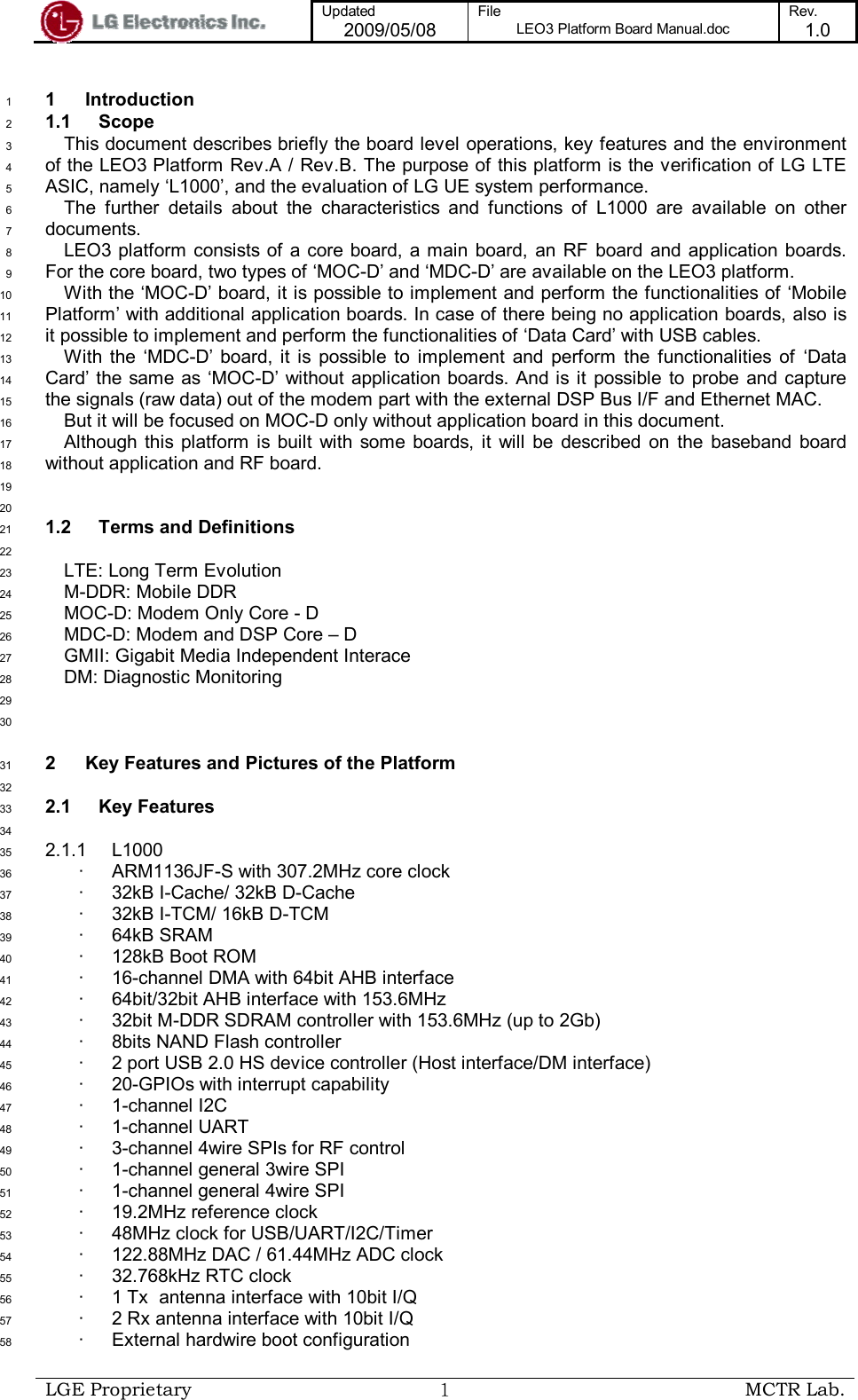
![Updated 2009/05/08 File LEO3 Platform Board Manual.doc Rev. 1.0 LGE Proprietary 8 MCTR Lab. SW4 No. Name Default Description 1 D_PHYAD(1) OFF 2 D_PHYAD(2) OFF 3 D_PHYAD(3) OFF 4 D_PHYAD(4) OFF D_PHYAD[4:1] [OFF] Ethernet PHY address value 1 [ON] Ethernet PHY address value 0 *ON: Low, OFF: High 5 D_ETH_MAN_MDIX OFF [OFF] Cross-over line mode [ON] Straight lien mode *ON: Low, OFF: High 6 D_ETH_MULTI_EN ON [OFF]: Multiple node (master) [ON]: Single node (slave) *ON: Low, OFF: High 7 D_ETH_MDIX_EN OFF [OFF]: Enable auto MDIX [ON]: Disable auto MDIX (set by D_ETH_MAN_MDIX) *ON: Low, OFF: High 8 DSP_PWRDOWN OFF [OFF]: DSP clock / reset enable [ON]: DSP clock / reset disable *ON: Low, OFF: High Table 4. DIP switch setting for Ethernet PHY 1 2](https://usermanual.wiki/LG-Electronics-USA/LEO3-BAND13/User-Guide-1114075-Page-28.png)
![Updated 2009/05/08 File LEO3 Platform Board Manual.doc Rev. 1.0 LGE Proprietary 9 MCTR Lab. 1 Jumper No. Name Default Description J3 UART_CTS/ UART_RTS 1-2 connection 3-4 connection [1-2, 3-4] for the cross UART cable [1-3, 2-4] for the straight UART cable J4 UART_RXD/ UART_TXD 1-2 connection 3-4 connection [1-2, 3-4] for the cross UART cable [1-3, 2-4] for the straight UART cable Table 5. Jumper setting for UART signal connection 2 3 5 LED Monitor 4 In the platform board, 15 LEDs are provided for the L1000 debug monitoring such as crash 5 debug, timing check, interrupt flag, status of L1000 etc. 6 The definition of monitor is not given yet for each LED explicitly. (TBD) 7 The LEDs for LED_DEBUG[0:7] and the LEDs for IRQ[0:3] are located lower left-hand corner 8 of the main board. 9 The LEDs for STATUS[0:2] are located lower right-hand corner of the main board. 10 All of them are indicated with white silkscreen printing on the main board respectively. 11 12 6 Image Downloading 13 If the other boot modes than ‘JTAG Boot’ such as ‘NAND Flash Boot’, ‘NOR Flash Boot’ are to 14 be used, they require the related image downloading into NAND flash or NOR flash. 15 For further information about the image downloading including the other boot load with USB or 16 SDIO, refer to other related documents. 17 18](https://usermanual.wiki/LG-Electronics-USA/LEO3-BAND13/User-Guide-1114075-Page-29.png)