LG Electronics USA LEO3-BAND13 LTE User Equipment User Manual
LG Electronics USA LTE User Equipment Users Manual
Users Manual

FCC ID : BEJLEO3-BAND13
HCT CO., LTD.
SAN 136-1, AMI-RI, BUBAL-EUP, ICHEON-SI, KYOUNGKI-DO, 467-701, KOREA
TEL:+82 31 639 8517 FAX:+82 31 639 8525 www.hct.co.kr
Report No. : HCT-RF09-0512 1/1
ATTACHMENT E.
- User Manual -
Updated
File
BAND13 RF board manual
Rev.
Written by
Reviewed by
Granted by
Managed by
Title
LEO3 RF (Band13) Hardware Manual
Type
Manual
LGE Proprietary i MCTR Lab.
ABSTRACT 1
This document is a hardware RF board manual for LTE user equipment platform. Contents of 2
this document are the description of each blocks and usage directions. It is recommended to 3
peruse this manual before operating RF Board. 4
5
HISTORY 6
Rev
Status
Date Author Contents
7
KEY WORDS 8
9
10
11
12
13
14
15
16
17
18
19
20
21
22
23
24
25
26
27
28
29
30
31
32
33
34
35
36
37
38
©Copyright, 2009 By LG Electronics Inc. All rights reserved.
No part of this document may be reproduced in any way, or by any means, without
the express written permission of LG Electronics Inc.
Mobile Communication Technology Research Lab.
533 Hogye-dong, Dongan-gu, Anyang-shi,
Kyongki-do, KOREA
Updated
File
BAND13 RF board manual
Rev.
LGE Proprietary ii MCTR Lab.
1
2
3
4
5
6
7
8
9
10
11
12
13
14
15
16
17
18
19
20
21
22
23
24
25
26
27
28
29
30
31
32
33
34
35
36
37
38
39
40
41
42
43
[Notice] 44
1. The product described in this manual may be modified without prior notice for reliability, 45
functionality or design improvement. 46
2. Information contained in this manual is correct and reliable, but LG shall not be held 47
responsible for damage due to the use of information, product or circuit or infringement of 48
property rights or other rights. 49
3. This manual does not grant users the property rights and other rights of the third party or LG 50
Electronics Inc. 51
4. No part of this manual may be transcribed or duplicated without the written permission of LG 52
Electronics Inc. 53
5. The appearance of the product shown in this manual may slightly differ from that of the actual 54
product. 55

Updated
File
BAND13 RF board manual
Rev.
LGE Proprietary iii MCTR Lab.
CONTENTS 1
1 Introduction................................................................................................................................ 1 2
1.1 Scope ..................................................................................................................................... 1 3
1.2 Terminology............................................................................................................................ 1 4
2 Features and Photograph........................................................................................................... 2 5
2.1 Features ................................................................................................................................. 2 6
2.2 Photograph of the LEO3 RF board.......................................................................................... 2 7
3 Block Diagram and Description.................................................................................................. 4 8
3.1 Block Diagram ........................................................................................................................ 4 9
3.2 Block Description .................................................................................................................... 4 10
3.2.1 RX Blocks................................................................................................................... 4 11
3.2.2 TX Blocks ................................................................................................................... 5 12
3.2.3 Common Blocks ......................................................................................................... 5 13
4 Interface .................................................................................................................................... 7 14
4.1 Power supply .......................................................................................................................... 7 15
4.2 Digital I/Q Data & Sampling Cock ........................................................................................... 8 16
4.3 SPI ......................................................................................................................................... 8 17
4.4 Control signals (GPIO’s).......................................................................................................... 9 18
4.5 LEDs....................................................................................................................................... 9 19
5 Placement Map....................................................................................................................... 10 20
21

Updated
File
BAND13 RF board manual
Rev.
LGE Proprietary iv MCTR Lab.
1
FIGURES 2
Figure 1: Photograph of LEO3 RF ................................................................................................... 3 3
Figure 2: RF Block Diagram (For RX/TX) ........................................................................................ 4 4
Figure 3: Diagrams of Power supply................................................................................................ 7 5
Figure 4: Diagrams of Data & Clock Signal Interface....................................................................... 8 6
Figure 5: Diagram of SPI interface .................................................................................................. 9 7
Figure 7: Top placement map of LEO3 RF (Band13).................................................................... 10 8
9
10
11
12
TABLES 13
Table 1: List of SPI programmable devices ..................................................................................... 8 14
15
16

Updated
File
BAND13 RF board manual
Rev.
LGE Proprietary 1
MCTR Lab.
1 Introduction 1
2
1.1 Scope 3
4
This RF board is intended for radio frequency part of LTE user equipment platform to develop 5
and verify LTE user equipment modem. This RF board is connected to 3rd version of LTE user 6
equipment platform (LEO3) as the form of daughter board. This document intends to describe the 7
brief architecture and usages of the board designed as RF part of LEO3 platform. 8
9
10
1.2 Terminology 11
12
ADC Analog to Digital Converter 13
AFC Automatic Frequency Compensation 14
DAC Digital to Analog Converter 15
LO Local Oscillator 16
LTE Long Term Evolution 17
LVDS Low-Voltage Differential Signaling 18
MISO Multi-In Single-Out 19
PA Power Amplifier 20
RF Radio Frequency 21
SAW Surface Acoustic Wave 22
UE User Equipment 23
VGA Variable Gain Amplifier 24

Updated
File
BAND13 RF board manual
Rev.
LGE Proprietary 2
MCTR Lab.
1
2 Features and Photograph 2
3
2.1 Features 4
5
Supporting RF band: BAND-13 6
Transmitting Frequency band: 777 ~ 787 MHz (10MHz) 7
Receiving Frequency band: 746 ~ 756 MHz (10MHz) 8
2-Receive path and 1-Transmit path (MISO) 9
+6V dc main power supply 10
19.2 MHz reference clock 11
Transceiver 12
Two chips transceiver solution by Infineon SMARTiLTE ICs(PMB_LTE_v093) 13
Triple-band operation 14
Three programmable LTE RF bandwidths: 5,10,20MHz 15
Supply voltage rage from 2.7 ~ 3.0V 16
Optional 2nd supply voltage from 1.71 ~ 3.0V 17
On-chip LDO 18
Different power-down modes 19
3-wire bus programmable 20
10-bit ADC and DAC support 21
61.44 MHz for AD conversion 22
122.88 MHz for DA conversion 23
Additional 16-bit HKDAC for Tx VGC and AFC 24
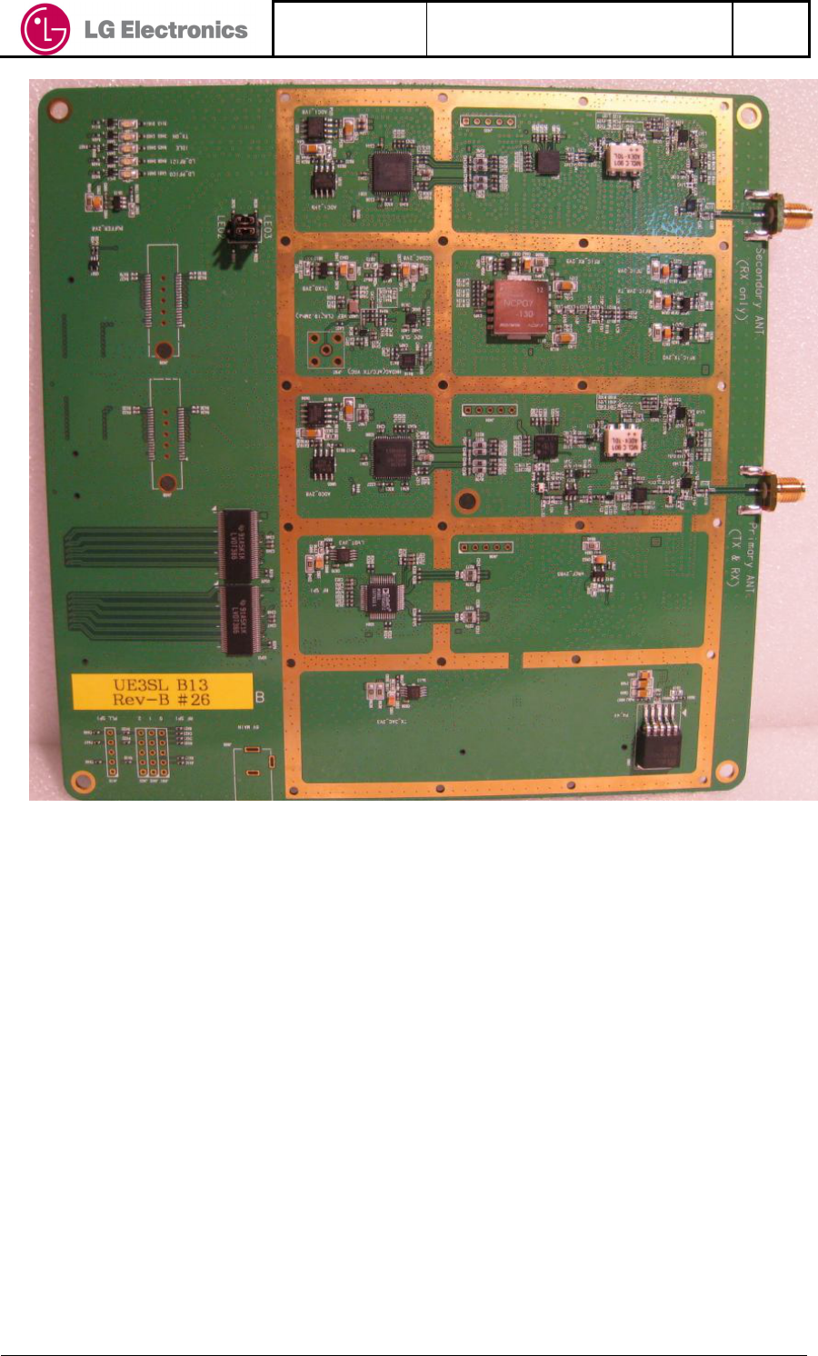
2.2 Photograph of the LEO3 RF board 25
26
Updated
File
BAND13 RF board manual
Rev.
LGE Proprietary 3
MCTR Lab.
1
2
Figure 1: Photograph of LEO3 RF 3
4
- Mechanical size of board is 170 (W) X 170 (H) mm5
Updated
File
BAND13 RF board manual
Rev.
LGE Proprietary 4
MCTR Lab.
1
3 Block Diagram and Description 2
3
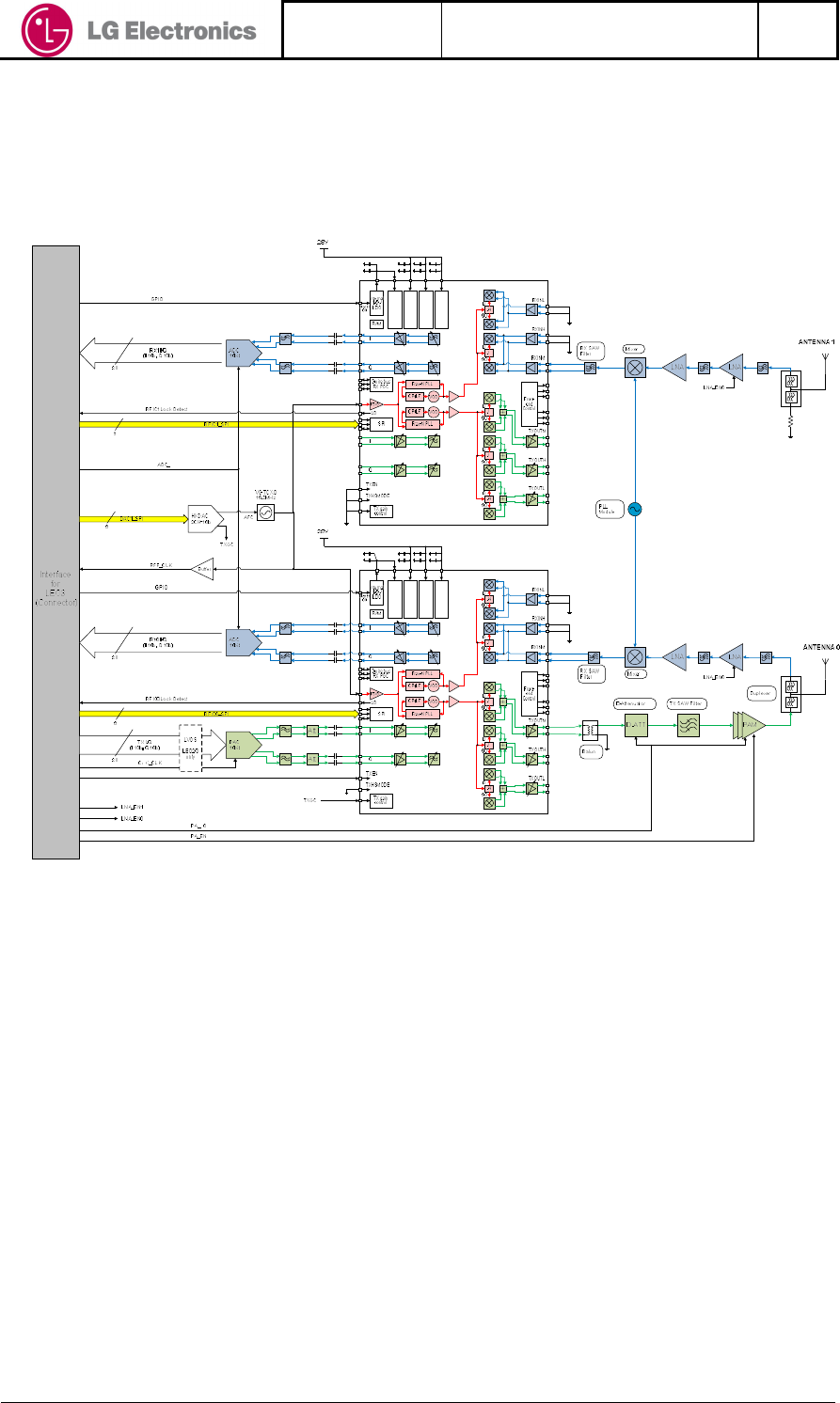
3.1 Block Diagram 4
5
6
2.7-3.0V
2.7-3.0V
1.71-3.0V
1.4-1.6V
2.7-3.0V
2.7-3.0V
1.71-3. 0V
1.4-1.6V
7
8
Figure 2: RF Block Diagram (For RX/TX) 9
10
3.2 Block Description 11
12
3.2.1 RX Blocks 13
14
Two receive paths, RX0 path and RX1 path, are designed for MISO technology to increase the 15
receiving data throughput. Both of receiving paths have the same structure and consist of the 16
following transceivers and anything else analog devices. 17
18
LNA 19
- This LNA is used for each receiving path 20
- LNA has the fixed 14dB gain at range of Band13 21
22
Transceiver (RX section) 23
- LNA2 with three programmable gain steps 24
- Complete analog baseband path without external components 25
- Three programmable baseband channel filter bandwidths 26
- Separate RX PGC 3-wire bus operation possible 27
- Performance 28
RX Total Gain : 2~80dB 29
Gain step: 1dB 30

Updated
File
BAND13 RF board manual
Rev.
LGE Proprietary 5
MCTR Lab.
Gain switching time: under 6 us 1
LNA2 Gain: 0/-6/-12 dB 2
Gain deviation: +/-3 dB 3
NFDSB:12dB – 42dB 4
IP1dB: -15dBm 5
6
ADC 7
- Dual 10-bit, 150MSPS analog-to-digital converter 8
- 10-bit dedicated for each I/Q data 9
- A/D clock speed: 61.44MHz 10
- Two’s complement data formatting 11
- Internal fixed reference mode (the input span is 2 Vp-p) 12
13
RX PLL 14
- A Module type consisting of PLL and VCO 15
- Programmalbe by 3 wire serial interface, SPI 16
17
18
3.2.2 TX Blocks 19
20
In transmit path, it is connected to a duplexer linked to ANT0. The transmitting data from LEO3 21
platform is the dedicated 10-bit digital signals for each I/Q via DAC. And its signaling uses LVDS 22
system for high speed data transmitting. Refer to the block diagram at section 2.3. The transmit 23
data pass through the following devices. 24
25
26
Level Translator 27
- High speed data level conversion, LVDS-to-CMOS 28
29
DAC 30
- Dual 10-bit, 125MSPS digital-to-analog converter 31
- 10-bit dedicated for each I/Q data 32
- D/A clock speed: 122.88MHz 33
- Offset binary data formatting 34
35
Transceiver (TX section) 36
- RF VGA’s with >85dB gain range 37
- Three programmable baseband filter bandwidths 38
- Performance 39
POUTmax: 3~7dBm 40
POUTmin: -77dBm 41
TXGC range:0.5V ~ 2.2V 42
Gain switching time:10usec 43
NTX: -136dBm/Hz 44
Carrier suppression:26dB 45
46
Digital Attenuator 47
- Single 10 dB Step 48
- Control voltage: -8.5V≤Vc≤+8V 49
- Low Loss: 0.3 dB @ 900 MHz 50
51
Power Amplifier 52
- Operating frequency: 1,710 ~ 1,785MHz 53
- Max output power: 28.5dBm 54
55
56
57
3.2.3 Common Blocks 58
59

Updated
File
BAND13 RF board manual
Rev.
LGE Proprietary 6
MCTR Lab.
VCTCXO 1
- AFC supported by the external gain control voltage 2
- Generating reference clock for transceiver 1st and 2nd respectively 3
- Generating reference clock for RX PLL 4
- Generating baseband clocks as the reference clock source 5
6
16-bit HKDAC for AFC and TX VGC control 7
- Dual channel 16-bit DAC 8
- Programmable by 3 wire serial interface, SPI 9
- Its analog output voltage level functions the following: 10
1) AFC support 11
2) VGA gain control at transmit path 12
Updated
File
BAND13 RF board manual
Rev.
LGE Proprietary 7
MCTR Lab.
1
4 Interface 2
3
The RF board for interfacing with LEO3 platform has 3 units of high speed 120pin connector. 4
One of them has the role for main power supply, 6V. The others make the interface between RF 5
to baseband (LEO3 platform) such as data transmitting and receiving, programming the SPI 6
device, transmitting control signals, supplying A/D or D/A clock, monitoring the status and etc. 7
8
4.1 Power supply 9
10
11
12
13
Figure 3: Diagrams of Power supply 14
Updated
File
BAND13 RF board manual
Rev.
LGE Proprietary 8
MCTR Lab.
1
4.2 Digital I/Q Data & Sampling Cock 2
3
4
5
6
Figure 4: Diagrams of Data & Clock Signal Interface 7
8
9
4.3 SPI 10
11
There are 3 programmable devices on RF board by using 3 wire SPI interface. 3 units SPI 12
blocks exist on the interface with baseband platform. They are listed at Table 1 (Also refer to 13
block diagram at Figure 5). 14
At this list, 1st transceiver and 2nd transceiver consist of each SPI0 and SPI1. Also 16-bit 15
HKDAC has the dedicated by SPI2. It can be possible by using a dedicated chip select signal for 16
each device with LLDM software. When selecting one of them, a dedicated chip select signal 17
enables its device to program. 18
19
20
21
22
23
24
25
Table 1: List of SPI programmable devices 26
SPI Device 1st Transceiver 2nd Transceiver 16bit-HKDAC
SPI block SPI0 SPI1 SPI2
SPI data bit - - 16
Updated
File
BAND13 RF board manual
Rev.
LGE Proprietary 9
MCTR Lab.
1
2
3
4
5
Figure 5: Diagram of SPI interface 6
7
8
4.4 Control signals (GPIO’s) 9
10
For control the RF blocks, the control signals from LEO3 platform are connected as the below. 11
12
- BS(1)_IDLE: Enables the LDOs and LED for a self-Indicator 13
- TX_ON: Enables the LDOs at transmit path and transmit block at 1st Transceiver (Including 14
turns on LED for a self-indicator) 15
- PA_R0 : Controls the power mode of transmitter block (Including D-attenuator) 16
- PA_EN : Enables PA 17
- LNA_EN0: Enables the LNA of antenna0 path (At the 1st transceiver) 18
- LNA_EN1: Enables the LNA of antenna1 path (At the 2nd transceiver) 19
- TCXO_ON: Enables the LDO for source clock (VC-TCXO) 20
- GPIO_SLEEPB(0): Enables the 1st transceiver (Via Master on signal) 21
- GPIO_SLEEPB(1): Enables the 2nd transceiver (Via Master on signal) 22
23
24
4.5 LEDs 25
26
To indicate PLL lock status of 1st transceiver(LD_RFIC0), 2nd transceiver(LD_RFIC1) and RX 27
PLL, three LEDs are present on the board. When locked at the frequency by setting the SPI from 28
LEO3, LD output of each Transceiver and RX PLL turns on these LEDs. 29
Anything else, there are two more LEDs(D4032 D403) for TX_ON and IDLE. 30
31
32
Updated
File
BAND13 RF board manual
Rev.
LGE Proprietary 10
MCTR Lab.
1
5 Placement Map 2
3
4
5
Figure 6: Top placement map of LEO3 RF (Band13) 6
7
Updated
File BAND13 RF board manual
LGE Proprietary 11 MCTR Lab.
Notice 1
2
OEM integrators and installers are instructed that the phrase. This device contains 3
4
Warning: Exposure to Radio Frequency Radiation The radiated output
power of this device is far below the FCC radio frequency exposure
limits. Nevertheless, the device should be used in such a manner that
the potential for human contact during normal operation is minimized.
In order to avoid the possibility of exceeding the FCC radio
frequency exposure limits, human proximity to the antenna should
not be less than 20cm during normal operation. The gain of the
antenna for 3GPP-Band13(777~787MHz) must not exceed -2.3 dBi.
The antenna(s) used for this transmitter must not be co-located or operating
in conjunction with any other antenna or transmitter.
Updated
2009/05/08
File
LEO3 Platform Board Manual.doc
Rev.
1.0
Written by
Reviewed by
Granted by
Managed by
Title
LEO3 Platform Board Manual
Type
Manual
LGE Proprietary i MCTR Lab.
ABSTRACT 1
2
3
HISTORY 4
Rev Status Date Author Contents
5
KEY WORDS 6
7
8
©Copyright, 2009 By LG Electronics Inc. All rights reserved.
No part of this document may be reproduced in any way, or by any means, without
the express written permission of LG Electronics Inc

Updated
2009/05/08
File
LEO3 Platform Board Manual.doc
Rev.
1.0
LGE Proprietary ii MCTR Lab.
CONTENTS 1
1 Introduction................................................................................................................................ 1 2
1.1 Scope ..................................................................................................................................... 1 3
1.2 Terms and Definitions............................................................................................................. 1 4
2 Key Features and Pictures of the Platform ................................................................................. 1 5
2.1 Key Features .......................................................................................................................... 1 6
2.1.1 L1000 ......................................................................................................................... 1 7
2.1.2 Memory ...................................................................................................................... 2 8
2.1.3 Other peripherals........................................................................................................ 2 9
2.2 Pictures and Placement of the Platform .................................................................................. 2 10
2.2.1 Pictures of LEO3 Platform .......................................................................................... 2 11
2.2.2 Placement Map........................................................................................................... 3 12
3 Power Supplies.......................................................................................................................... 4 13
3.1 Main Board Power................................................................................................................... 4 14
3.2 RF Board Power ..................................................................................................................... 4 15
3.3 L1000...................................................................................................................................... 4 16
3.4 Other Peripherals.................................................................................................................... 4 17
4 Switch Setting............................................................................................................................ 4 18
5 LED Monitor............................................................................................................................... 7 19
6 Image Downloading ................................................................................................................... 7 20
21

Updated
2009/05/08
File
LEO3 Platform Board Manual.doc
Rev.
1.0
LGE Proprietary iii MCTR Lab.
1
FIGURES 2
Figure 1. LEO3 Platform (Top Side) ................................................................................................ 2 3
Figure 2. LEO3 Platform (Bottom Side)........................................................................................... 3 4
Figure 3. LEO3 Platform Board Layout............................................................................................ 3 5
6

Updated
2009/05/08
File
LEO3 Platform Board Manual.doc
Rev.
1.0
LGE Proprietary iv MCTR Lab.
1
TABLES 2
Table 1. DIP switch setting for L1000 boot configuration ................................................................. 5 3
Table 2. DIP switch setting for manual IRQ generation.................................................................... 5 4
Table 3. DIP switch setting for LED_DEBUG................................................................................... 6 5
Table 4. DIP switch setting for Ethernet PHY................................................................................... 6 6
Table 5. Jumper setting for UART signal connection ....................................................................... 7 7
8
9

Updated
2009/05/08
File
LEO3 Platform Board Manual.doc
Rev.
1.0
LGE Proprietary 1
MCTR Lab.
1 Introduction 1
1.1 Scope 2
This document describes briefly the board level operations, key features and the environment 3
of the LEO3 Platform Rev.A / Rev.B. The purpose of this platform is the verification of LG LTE 4
ASIC, namely ‘L1000’, and the evaluation of LG UE system performance. 5
The further details about the characteristics and functions of L1000 are available on other 6
documents. 7
LEO3 platform consists of a core board, a main board, an RF board and application boards. 8
For the core board, two types of ‘MOC-D’ and ‘MDC-D’ are available on the LEO3 platform. 9
With the ‘MOC-D’ board, it is possible to implement and perform the functionalities of ‘Mobile 10
Platform’ with additional application boards. In case of there being no application boards, also is 11
it possible to implement and perform the functionalities of ‘Data Card’ with USB cables. 12
With the ‘MDC-D’ board, it is possible to implement and perform the functionalities of ‘Data 13
Card’ the same as ‘MOC-D’ without application boards. And is it possible to probe and capture 14
the signals (raw data) out of the modem part with the external DSP Bus I/F and Ethernet MAC. 15
But it will be focused on MOC-D only without application board in this document. 16
Although this platform is built with some boards, it will be described on the baseband board 17
without application and RF board. 18
19
20
1.2 Terms and Definitions 21
22
LTE: Long Term Evolution 23
M-DDR: Mobile DDR 24
MOC-D: Modem Only Core - D 25
MDC-D: Modem and DSP Core – D 26
GMII: Gigabit Media Independent Interace 27
DM: Diagnostic Monitoring 28
29
30
2 Key Features and Pictures of the Platform 31
32
2.1 Key Features 33
34
2.1.1 L1000 35
· ARM1136JF-S with 307.2MHz core clock 36
· 32kB I-Cache/ 32kB D-Cache 37
· 32kB I-TCM/ 16kB D-TCM 38
· 64kB SRAM 39
· 128kB Boot ROM 40
· 16-channel DMA with 64bit AHB interface 41
· 64bit/32bit AHB interface with 153.6MHz 42
· 32bit M-DDR SDRAM controller with 153.6MHz (up to 2Gb) 43
· 8bits NAND Flash controller 44
· 2 port USB 2.0 HS device controller (Host interface/DM interface) 45
· 20-GPIOs with interrupt capability 46
· 1-channel I2C 47
· 1-channel UART 48
· 3-channel 4wire SPIs for RF control 49
· 1-channel general 3wire SPI 50
· 1-channel general 4wire SPI 51
· 19.2MHz reference clock 52
· 48MHz clock for USB/UART/I2C/Timer 53
· 122.88MHz DAC / 61.44MHz ADC clock 54
· 32.768kHz RTC clock 55
· 1 Tx antenna interface with 10bit I/Q 56
· 2 Rx antenna interface with 10bit I/Q 57
· External hardwire boot configuration 58
Updated
2009/05/08
File
LEO3 Platform Board Manual.doc
Rev.
1.0
LGE Proprietary 2
MCTR Lab.
· Debugger port (JTAG + ETM11) 1
2
2.1.2 Memory 3
· MCP with 2Gb 8bit NAND flash / DDR333 1Gb 32bit M-DDR 4
· 64Mb Serial NOR flash (4wire SPI) 5
6
2.1.3 Other peripherals 7
· PMIC for evaluation and feasibility check 8
· 2-USB connectors 9
· LVDS drivers for 10bit I/Q Tx signal and DAC clock 10
· Application board interface (unavailable in this document) 11
· 1-channel SIM connector 12
· 1-channel 4bit SDIO connector (only available for MDC-D core board) 13
· JTAG/ETM 11 debug ports for ARM (ETM clock with 76.8MHz) 14
· JTAG debug port for DSP (only available for MDC-D core board) 15
· 1-Gigabit Ethernet (GMII mode) connector for DSP (only available for MDC-D core 16
board) 17
· RF interface with connector (bottom side) 18
· Reset switch for global hardware reset 19
· 15 LEDs and 2 DIP-switches for debug 20
· 5 LEDs for Ethernet mode monitor (only available for MDC-D core board) 21
· 8 LEDs for DSP GPIO (only available for MDC-D core board) 22
· 2 DIP-switches for boot configuration setting 23
24
25
2.2 Pictures and Placement of the Platform 26
27
2.2.1 Pictures of LEO3 Platform 28
29
30
31
32
Figure 1. LEO3 Platform (Top Side) 33
34
+12V
Power
SW.
SIM
L1000
JTAG
UART
USB
ETM11
LEDs
DIP SW
.
LEDs
Updated
2009/05/08
File
LEO3 Platform Board Manual.doc
Rev.
1.0
LGE Proprietary 3
MCTR Lab.
1
2
Figure 2. LEO3 Platform (Bottom Side) 3
4
2.2.2 Placement Map 5
6
Figure 3. LEO3 Platform Board Layout 7
Rx1 ANT
Rx0/ Tx ANT

Updated
2009/05/08
File
LEO3 Platform Board Manual.doc
Rev.
1.0
LGE Proprietary 4
MCTR Lab.
1
3 Power Supplies 2
3
3.1 Main Board Power 4
Main external power is supplied from DC input jack on the upper left corner of the baseband 5
platform board. The regular input voltage is 12V. For this platform, an external power adaptor 6
‘CLG-60-12’ from Mean Well is provided with maximum current rating of 5A. 7
8
9
3.2 RF Board Power 10
The RF board power is supplied from the mian board RF connector. 11
The regular RF board input voltage is 6V, which is regulated from the main board power so an 12
additional power supply for RF board is not required. 13
14
15
3.3 L1000 16
· Core Power - +1.2V 17
· Memory controller / Flash controller power - +1.8V 18
· I/O Power - +2.8V 19
· USB Power - +3.3V 20
21
3.4 Other Peripherals 22
· L1000 I/O power - +2.8V 23
· LVDS driver Power - +3.3V 24
· Reset Power - +2.8V 25
· SIM L/T Output Power - +1.8V / +3.0V 26
· Ethernet Transceiver Analog Power - +1.8V / +2.5V (only available for MDC-D core 27
board) 28
· Ethernet I/O Power - +3.3V (only available for MDC-D core board) 29
· DSP Core Power - +1.25V (only available for MDC-D core board) 30
· DSP Memory Controller Power - +1.8V (only available for MDC-D core board) 31
32
33
4 Switch Setting 34
35
Configuration and control settings are done by 5-DIP switches (SW4, SW5, SW6, SW7, SW8) 36
and 2 jumpers (J3, J4). The assignments of each signal and their descriptions are in the following 37
tables. 38
39
Updated
2009/05/08
File
LEO3 Platform Board Manual.doc
Rev.
1.0
LGE Proprietary 5
MCTR Lab.
1
SW7
No.
Name Defaul
t
Description
1 JTAG_CFG(0) ON
2 JTAG_CFG(1) OFF
JTAG_CFG[1:0]
[OFF:OFF] No JTAG
[OFF:ON] ARM Only
[ON:OFF] CC5 Only
[ON:ON] ARM-CC5
*ON: High, OFF: Low
3 EPI_MODE ON [OFF] Dedicated Address/Data EPI I/O
[ON] Muxed Address/Data EPI I/O
*ON: HIgh, OFF: Low
4 USB_MODE OFF [OFF] UTMI mode
[ON] ULPI mode
*ON: High OFF: Low
5 PWR_CUT_MODE OFF [OFF] Power cut disable
[ON] Power cut enable
*ON: High, OFF: Low
6 REFCLK_SEL OFF [OFF] On-board VCTCXO 19.2MHz
[ON] RF board 19.2MHz
*ON: High, OFF: Low (Rev.A)
*ON: Low, OFF: High (Rev.B)
7 NAND_CFG(0) OFF [ON] 4byte address
[OFF] 5byte address
*ON: Low, OFF: High
8 NAND_CFG(1) OFF [ON] Small block (1page: 512byte + 16byte)
[OFF] Large block (1page 2048byte +64byte)
*ON: Low, OFF: High
SW8
No.
Name Defaul
t
Description
1 MODE(0) ON
2 MODE(1) OFF
3 MDOE(2) OFF
MODE[2:0]
[OFF:OFF:OFF] Undefined
[OFF:OFF:ON] NAND boot
[OFF:ON:OFF] Serial Flash boot
[OFF:ON:ON] EPI boot
[ON:OFF:OFF] SDIO boot
[ON:OFF:ON] USB boot
[ON:ON:OFF] Serial Flash boot (for debug)
[ON:ON:ON] Test
*ON: High, OFF: Low
4 MODE(3) OFF [OFF] Secure Boot disable
[ON] Secure Boot enable
*ON: High OFF: Low
Table 1. DIP switch setting for L1000 boot configuration 2
3
4
Updated
2009/05/08
File
LEO3 Platform Board Manual.doc
Rev.
1.0
LGE Proprietary 6
MCTR Lab.
SW6
No.
Name Defaul
t
Description
1 IRQ(0) OFF [OFF] Low level
[ON] High level
*ON: High, OFF: Low
2 IRQ(1) OFF [OFF] High level (Rev.A), Low level (Rev.B)
[ON] Low level (Rev.A), High level (Rev.B)
*ON: High, OFF: Low (Rev.A)
*ON: Low, OFF: High (Rev.B)
3 IRQ(2) OFF [OFF] High level
[ON] Low level
*ON: Low, OFF: High
4 IRQ(3) OFF [OFF] High level
[ON] Low level
*ON: Low, OFF: High
Table 2. DIP switch setting for manual IRQ generation 1
2
Updated
2009/05/08
File
LEO3 Platform Board Manual.doc
Rev.
1.0
LGE Proprietary 7
MCTR Lab.
1
* Caution) Please, be careful to switch ‘ON” for the SW5. Switching ‘ON’ should be done 2
only when the corresponding GPIO directions have defined as ‘Input’. Otherwise (if 3
defined as ‘Output’), it would be possible for the L1000 to have a damage. 4
SW5
No.
Name Defaul
t
Description
1 LED_DEBUG(0) OFF Corresponding to GPIO(0) of L1000
[OFF] Low level
[ON] High level
*ON: High, OFF: Low
2 LED_DEBUG(1) OFF Corresponding to GPIO(1) of L1000
[OFF] Low level
[ON] High level
*ON: High, OFF: Low
3 LED_DEBUG(2) OFF Corresponding to GPIO(2) of L1000
[OFF] Low level
[ON] High level
*ON: High, OFF: Low
4 LED_DEBUG(3) OFF Corresponding to GPIO(3) of L1000
[OFF] Low level
[ON] High level
*ON: High, OFF: Low
5 LED_DEBUG(4) OFF Corresponding to GPIO(4) of L1000
[OFF] Low level
[ON] High level
*ON: High, OFF: Low
6 LED_DEBUG(5) OFF Corresponding to GPIO(5) of L1000
[OFF] Low level
[ON] High level
*ON: High, OFF: Low
7 LED_DEBUG(6) OFF Corresponding to GPIO(6) of L1000
[OFF] Low level
[ON] High level
*ON: High, OFF: Low
8 LED_DEBUG(7) OFF Corresponding to GPIO(7) of L1000
[OFF] Low level
[ON] High level
*ON: High, OFF: Low
Table 3. DIP switch setting for LED_DEBUG 5
6
7
* SW4 is not available for MOC-D core board 8
Updated
2009/05/08
File
LEO3 Platform Board Manual.doc
Rev.
1.0
LGE Proprietary 8
MCTR Lab.
SW4
No.
Name Defaul
t
Description
1 D_PHYAD(1) OFF
2 D_PHYAD(2) OFF
3 D_PHYAD(3) OFF
4 D_PHYAD(4) OFF
D_PHYAD[4:1]
[OFF] Ethernet PHY address value 1
[ON] Ethernet PHY address value 0
*ON: Low, OFF: High
5 D_ETH_MAN_MDIX
OFF [OFF] Cross-over line mode
[ON] Straight lien mode
*ON: Low, OFF: High
6 D_ETH_MULTI_EN
ON [OFF]: Multiple node (master)
[ON]: Single node (slave)
*ON: Low, OFF: High
7 D_ETH_MDIX_EN OFF [OFF]: Enable auto MDIX
[ON]: Disable auto MDIX (set by D_ETH_MAN_MDIX)
*ON: Low, OFF: High
8 DSP_PWRDOWN OFF [OFF]: DSP clock / reset enable
[ON]: DSP clock / reset disable
*ON: Low, OFF: High
Table 4. DIP switch setting for Ethernet PHY 1
2
Updated
2009/05/08
File
LEO3 Platform Board Manual.doc
Rev.
1.0
LGE Proprietary 9
MCTR Lab.
1
Jumper No.
Name Default Description
J3 UART_CTS/
UART_RTS
1-2 connection
3-4 connection
[1-2, 3-4] for the cross UART cable
[1-3, 2-4] for the straight UART cable
J4 UART_RXD/
UART_TXD
1-2 connection
3-4 connection
[1-2, 3-4] for the cross UART cable
[1-3, 2-4] for the straight UART cable
Table 5. Jumper setting for UART signal connection 2
3
5 LED Monitor 4
In the platform board, 15 LEDs are provided for the L1000 debug monitoring such as crash 5
debug, timing check, interrupt flag, status of L1000 etc. 6
The definition of monitor is not given yet for each LED explicitly. (TBD) 7
The LEDs for LED_DEBUG[0:7] and the LEDs for IRQ[0:3] are located lower left-hand corner 8
of the main board. 9
The LEDs for STATUS[0:2] are located lower right-hand corner of the main board. 10
All of them are indicated with white silkscreen printing on the main board respectively. 11
12
6 Image Downloading 13
If the other boot modes than ‘JTAG Boot’ such as ‘NAND Flash Boot’, ‘NOR Flash Boot’ are to 14
be used, they require the related image downloading into NAND flash or NOR flash. 15
For further information about the image downloading including the other boot load with USB or 16
SDIO, refer to other related documents. 17
18